high-density stm32f103xx die specification hi...data brief for further information contact your...
TRANSCRIPT

Data brief
For further information contact your local STMicroelectronics sales office.
November 2009 Doc ID 16595 Rev 2 1/25
1
STM32F103EDIE
High-density STM32F103xx die specification
Features■ Wafer size: 8 inches
■ Die identification: T414A
■ Die stepping (X,Y): 4511, 4440 µm
■ Wafer thickness: 381 ± 25 µm
■ Scribe street (X,Y): 80, 80 µm
■ Die finish front side: polyimide
■ Die finish back side: raw silicon
■ Wafer type (Si, GaAs, Others): Si
■ Process type: CMOS
■ Pad number per die: 154
■ Laser trimming: not applicable
1. For the Diffusion lot identification, refer to Diffusion lot identification on page 13.
Diffusion lotidentification(1)
ai14697
Notch
Diffusion lotidentification(1)
ai14698
Notch
www.st.com

Contents STM32F103EDIE
2/25 Doc ID 16595 Rev 2
Contents
1 Die description . . . . . . . . . . . . . . . . . . . . . . . . . . . . . . . . . . . . . . . . . . . . . 5
1.1 Wafer processing and assembly . . . . . . . . . . . . . . . . . . . . . . . . . . . . . . . . 6
1.1.1 Good dice . . . . . . . . . . . . . . . . . . . . . . . . . . . . . . . . . . . . . . . . . . . . . . . . 6
1.1.2 Back-lapping . . . . . . . . . . . . . . . . . . . . . . . . . . . . . . . . . . . . . . . . . . . . . . 6
1.1.3 Assembly . . . . . . . . . . . . . . . . . . . . . . . . . . . . . . . . . . . . . . . . . . . . . . . . . 6
1.2 Ordering information . . . . . . . . . . . . . . . . . . . . . . . . . . . . . . . . . . . . . . . . 13
1.2.1 Diffusion lot identification . . . . . . . . . . . . . . . . . . . . . . . . . . . . . . . . . . . . 13
2 Die layout . . . . . . . . . . . . . . . . . . . . . . . . . . . . . . . . . . . . . . . . . . . . . . . . . 14
3 Pad coordinates . . . . . . . . . . . . . . . . . . . . . . . . . . . . . . . . . . . . . . . . . . . 16
4 Specific warning for die handling . . . . . . . . . . . . . . . . . . . . . . . . . . . . . 22
4.1 Assembly qualification . . . . . . . . . . . . . . . . . . . . . . . . . . . . . . . . . . . . . . . 22
4.2 Traceability . . . . . . . . . . . . . . . . . . . . . . . . . . . . . . . . . . . . . . . . . . . . . . . . 22
4.3 Failure analysis . . . . . . . . . . . . . . . . . . . . . . . . . . . . . . . . . . . . . . . . . . . . 22
4.4 Flash memory recommendations . . . . . . . . . . . . . . . . . . . . . . . . . . . . . . . 23
4.5 Guarantee . . . . . . . . . . . . . . . . . . . . . . . . . . . . . . . . . . . . . . . . . . . . . . . . 23
5 Revision history . . . . . . . . . . . . . . . . . . . . . . . . . . . . . . . . . . . . . . . . . . . 24

STM32F103EDIE List of tables
Doc ID 16595 Rev 2 3/25
List of tables
Table 1. Wire bond pad metal. . . . . . . . . . . . . . . . . . . . . . . . . . . . . . . . . . . . . . . . . . . . . . . . . . . . . . . 5Table 2. Assembly features (critical dimensions) . . . . . . . . . . . . . . . . . . . . . . . . . . . . . . . . . . . . . . . . 5Table 3. Ordering information . . . . . . . . . . . . . . . . . . . . . . . . . . . . . . . . . . . . . . . . . . . . . . . . . . . . . . 13Table 4. HSI oscillator accuracy . . . . . . . . . . . . . . . . . . . . . . . . . . . . . . . . . . . . . . . . . . . . . . . . . . . 13Table 5. Pad coordinates . . . . . . . . . . . . . . . . . . . . . . . . . . . . . . . . . . . . . . . . . . . . . . . . . . . . . . . . . 16Table 6. Document revision history . . . . . . . . . . . . . . . . . . . . . . . . . . . . . . . . . . . . . . . . . . . . . . . . . 24
List of figures STM32F103EDIE
4/25 Doc ID 16595 Rev 2
List of figures
Figure 1. Pad diagram . . . . . . . . . . . . . . . . . . . . . . . . . . . . . . . . . . . . . . . . . . . . . . . . . . . . . . . . . . . . . 5Figure 2. Bonding diagram for LQFP144 . . . . . . . . . . . . . . . . . . . . . . . . . . . . . . . . . . . . . . . . . . . . . . . 7Figure 3. LQFP144 pinout . . . . . . . . . . . . . . . . . . . . . . . . . . . . . . . . . . . . . . . . . . . . . . . . . . . . . . . . . . 8Figure 4. Bonding diagram for LQFP100 . . . . . . . . . . . . . . . . . . . . . . . . . . . . . . . . . . . . . . . . . . . . . . . 9Figure 5. LQFP100 pinout . . . . . . . . . . . . . . . . . . . . . . . . . . . . . . . . . . . . . . . . . . . . . . . . . . . . . . . . . 10Figure 6. Bonding diagram for LQFP64 . . . . . . . . . . . . . . . . . . . . . . . . . . . . . . . . . . . . . . . . . . . . . . . 11Figure 7. LQFP64 pinout . . . . . . . . . . . . . . . . . . . . . . . . . . . . . . . . . . . . . . . . . . . . . . . . . . . . . . . . . . 12Figure 8. Illustration of the diffusion lot identification . . . . . . . . . . . . . . . . . . . . . . . . . . . . . . . . . . . . . 13Figure 9. Die layout / notch position. . . . . . . . . . . . . . . . . . . . . . . . . . . . . . . . . . . . . . . . . . . . . . . . . . 14Figure 10. Scribing street and stepping die size definition. . . . . . . . . . . . . . . . . . . . . . . . . . . . . . . . . . 14Figure 11. Ring drawing for 8” wafer . . . . . . . . . . . . . . . . . . . . . . . . . . . . . . . . . . . . . . . . . . . . . . . . . . 15

STM32F103EDIE Die description
Doc ID 16595 Rev 2 5/25
1 Die description
Important note: Refer to Section 4 for specific handling terms and conditions.
I/O type: CUP (circuit under pad).
Figure 1. Pad diagram
Table 1. Wire bond pad metal
Wire bond pad metal Composition Thickness (µm)
Metal 1 Tin/AlCu/Tin 0.45
Metal 2 Tin/AlCu/Tin 0.45
Metal 3 Tin/AlCu/Tin 0.45
Metal 4 Tin/AlCu/Tin 0.45
Metal 5 Tin/AlCu/Tin 0.875
Pad size X = 75 µm, Y = 80 µm
Passivation opening X = 65 µm, Y = 70 µm
Minimum passivation and pad overlap 5 µm for one side
Table 2. Assembly features (critical dimensions)
Wire quantityWire material
typeWire
diameterBond pad
windows (X,Y)Minimum
pitchWire bond pad
placement
N/A N/A 25 µm 65.70 µm 80 µm 100%
Passivation
Passivationoverlap
Passivationopening
Pad size
Inter metal
Metal layer
ai14699

Die description STM32F103EDIE
6/25 Doc ID 16595 Rev 2
1.1 Wafer processing and assembly
1.1.1 Good dice
The wafers are ink marked. All dice which are not good are marked with an ink spot.
1.1.2 Back-lapping
Back-lapping is permitted on these wafers to reduce wafer thickness. ST does not perform additional back-lapping in house for these products, it has to be done by a sub-contractor.
1.1.3 Assembly
Please refer to the following package bonding and package pin-out for pad / pin relation.
The Autocad or GDS files of pad opening are available upon request:
Number of chips per wafer Gross chips: 1379
Good chips: > 1170 (85% on average)
Minimum thickness allowed: 150 µm
GDS file
Autocad file

STM32F103EDIE Die description
Doc ID 16595 Rev 2 7/25
Figure 2. Bonding diagram for LQFP144
Frame pad: 236 × 236 mils6.00 × 6.00 mm
Die size: 4510 × 4440 µm
ai15456

Die description STM32F103EDIE
8/25 Doc ID 16595 Rev 2
Figure 3. LQFP144 pinout
VD
D_3
VS
S_3
PE
1P
E0
PB
9P
B8
BO
OT
0P
B7
PB
6P
B5
PB
4P
B3
PG
15V
DD
_11
VS
S_1
1P
G14
PG
13P
G12
PG
11P
G10
PG
9P
D7
PD
6V
DD
_10
VS
S_1
0P
D5
PD
4P
D3
PD
2P
D1
PD
0P
C12
PC
11P
C10
PA
15P
A14
PE2 VDD_2PE3 VSS_2PE4 NCPE5 PA13PE6 PA12
VBAT PA11PC13-TAMPER-RTC PA10
PC14-OSC32_IN PA9PC15-OSC32_OUT PA8
PF0 PC9PF1 PC8PF2 PC7PF3 PC6PF4 VDD_9PF5 VSS_9
VSS_5 PG8VDD_5 PG7
PF6 PG6PF7 PG5PF8 PG4PF9 PG3
PF10 PG2OSC_IN PD15
OSC_OUT PD14NRST VDD_8
PC0 VSS_8PC1 PD13PC2 PD12PC3 PD11
VSSA PD10VREF- PD9VREF+ PD8VDDA PB15
PA0-WKUP PB14PA1 PB13PA2 PB12
PA
3V
SS
_4V
DD
_4 PA
4P
A5
PA
6P
A7
PC
4P
C5
PB
0P
B1
PB
2P
F11
PF
12
VS
S_6
VD
D_6
PF
13P
F14
PF
15P
G0
PG
1P
E7
PE
8P
E9
VS
S_7
VD
D_7
PE
10P
E11
PE
12P
E13
PE
14P
E15
PB
10P
B11
VS
S_1
VD
D_1
144
143
142
141
140
139
138
137
136
135
134
133
132
131
130
129
128
127
126
125
124
123
122
121
109
12345678910111213141516171819202122232425
108107106105104103102101100
99989796959493929190898887868584
37 38 39 40 41 42 43 44 45 46 47 48 49 50 51 52 53 54 55 56 57 58 59 60 72
LQFP144
120
119
118
117
116
115
114
113
112
111
110
61 62 63 64 65 66 67 68 69 70 71
2627282930313233343536
8382818079787776757473
ai14667b

STM32F103EDIE Die description
Doc ID 16595 Rev 2 9/25
Figure 4. Bonding diagram for LQFP100
Frame pad: 0.284 × 0.284 inch7.2 × 7.2 mm 1 mm
GND bond authorized only in the delimited area
Pin 1
100 95 90 85 80 76
75
70
65
60
55
51
504540353026
25
20
15
10
5
1
Die ID
ai15457

Die description STM32F103EDIE
10/25 Doc ID 16595 Rev 2
Figure 5. LQFP100 pinout
Warning: The supported die is as follows: 512 KB on 144 pins, one bonding, one memory footprint. The application must configure by software the unused pins for bondings below 144 pins.
100
99 98 97 96 95 94 93 92 91 90 89 88 87 86 85 84 83 82 81 80 79 78 77 76
12345678910111213141516171819202122232425
75747372717069686766656463626160595857565554535251
VDD_2 VSS_2 NC PA 13 PA 12 PA 11 PA 10 PA 9 PA 8 PC9 PC8 PC7 PC6 PD15 PD14 PD13 PD12 PD11 PD10 PD9 PD8 PB15 PB14 PB13 PB12
PA3
VS
S_4
VD
D_4
PA4
PA5
PA6
PA7
PC
4P
C5
PB
0P
B1
PB
2P
E7
PE
8P
E9
PE
10P
E11
PE
12P
E13
PE
14P
E15
PB
10P
B11
VS
S_1
VD
D_1
VD
D_3
V
SS
_3
PE
1
PE
0
PB
9
PB
8
BO
OT
0
PB
7
PB
6
PB
5
PB
4
PB
3
PD
7
PD
6
PD
5
PD
4
PD
3
PD
2
PD
1
PD
0
PC
12
PC
11
PC
10
PA15
PA
14
26 27 28 29 30 31 32 33 34 35 36 37 38 39 40 41 42 43 44 45 46 47 48 49 50
PE2PE3PE4PE5PE6
VBATPC13-TAMPER-RTC
PC14-OSC32_INPC15-OSC32_OUT
VSS_5VDD_5
OSC_INOSC_OUT
NRSTPC0PC1PC2PC3
VSSAVREF-VREF+VDDA
PA0-WKUPPA1PA2
ai14391
LQFP100

STM32F103EDIE Die description
Doc ID 16595 Rev 2 11/25
Figure 6. Bonding diagram for LQFP64
Frame pad: 0.236 × 0.236 inch5.994 × 5.994 mm
1 mm
Pin 1
64 63 62 61 60 59 58 57 56 55 54 53 52 51 50 49
17 18 19 20 21 22 23 24 25 26 27 28 29 30 31 32
33
34
35
36
37
38
39
40
41
42
43
44
45
46
47
48
16
15
14
13
12
11
10
9
8
7
6
5
4
3
2
1
Die ID
ai15458

Die description STM32F103EDIE
12/25 Doc ID 16595 Rev 2
Figure 7. LQFP64 pinout
Warning: The supported die is as follows: 512 KB on 144 pins, one bonding, one memory footprint. The application must configure by software the unused pins for bondings below 144 pins.
64 63 62 61 60 59 58 57 56 55 54 53 52 51 50 494847
46 45 44 4342414039383736353433
17 18 19 20 21 22 23 24 29 30 31 3225 26 27 28
123456 7 8 9 1011 12 13141516
VBATPC13-TAMPER-RTC
PC14-OSC32_INPC15-OSC32_OUT
PD0 OSC_INPD1 OSC_OUT
NRSTPC0PC1PC2PC3
VSSAVDDA
PA0-WKUPPA1PA2
VD
D_3
VS
S_3
PB
9
PB
8
BO
OT
0
PB
7
PB
6
PB
5
PB
4
PB
3
PD
2
PC
12
PC
11
PC
10
PA15
PA
14
VDD_2 VSS_2PA13 PA12 PA11 PA10 PA9 PA8 PC9 PC8 PC7 PC6 PB15 PB14 PB13 PB12
PA3
VS
S_4
VD
D_4
PA4
PA5
PA6
PA7
PC
4P
C5
PB
0P
B1
PB
2P
B10
PB
11V
SS
_1V
DD
_1
LQFP64
ai14392

STM32F103EDIE Die description
Doc ID 16595 Rev 2 13/25
1.2 Ordering information
Note: For electrical and functional information, please refer to the datasheet and reference manual of the equivalent packaged part. The electrical characteristics are the same, with a restricted temperature range, except for a few parameters.The values that change are specified in Table 4 below. For other characteristics, please refer to the high-density STM32F103xCDE datasheet available from the STMicroelectronics website: www.st.com.
1.2.1 Diffusion lot identification
The lot is identified by the “source lot” numbers and the first 2 digits of the wafer code as shown below.
Figure 8. Illustration of the diffusion lot identification
Table 3. Ordering information
Die part number Sales typeTemperature
rangeEquivalent
packaged part
Flash program memory (Kbytes)
SRAM memory (Kbytes)
Number of pins
STM32F103EDIE STM32F103EDIE1 –40 °C to +85 °C STM32F103ZET6 512 64 144
Table 4. HSI oscillator accuracy(1) (2)
1. Guaranteed by design, not tested in production.
2. VDD = 3.3 V.
Symbol Parameter Conditions Max Unit
ACCHSI Accuracy of HSI oscillator TA = –40 to 85 °C 3.5 %
Source lot codegiven on the shielding bag first 2 digits of the wafer code
C X X X X X
AI14702

Die layout STM32F103EDIE
14/25 Doc ID 16595 Rev 2
2 Die layout
Figure 9. Die layout / notch position
Figure 10. Scribing street and stepping die size definition
notchai15459
Die ID
1
154 117
116
X
Y
38
39 78
79
X
Y
Die
Wafer
Scribing street
Stepping die size
Saw cut widthor Kerf width
Notch
ai14703

STM32F103EDIE Die layout
Doc ID 16595 Rev 2 15/25
Figure 11. Ring drawing for 8” wafer
Material : stainless steelThickness:1.5mm (All dimensions in mm)
Pad coordinates STM32F103EDIE
16/25 Doc ID 16595 Rev 2
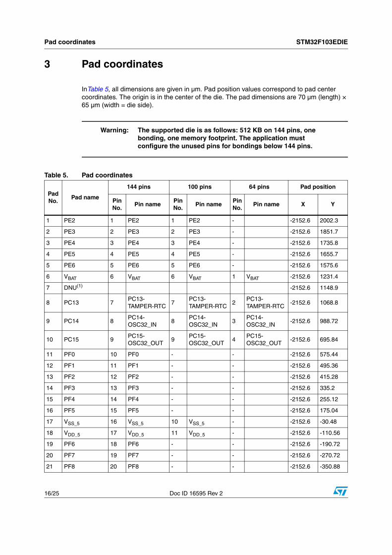
3 Pad coordinates
InTable 5, all dimensions are given in µm. Pad position values correspond to pad center coordinates. The origin is in the center of the die. The pad dimensions are 70 µm (length) × 65 µm (width = die side).
Warning: The supported die is as follows: 512 KB on 144 pins, one bonding, one memory footprint. The application must configure the unused pins for bondings below 144 pins.
Table 5. Pad coordinates
Pad No.
Pad name
144 pins 100 pins 64 pins Pad position
Pin No.
Pin namePin No.
Pin namePin No.
Pin name X Y
1 PE2 1 PE2 1 PE2 - -2152.6 2002.3
2 PE3 2 PE3 2 PE3 - -2152.6 1851.7
3 PE4 3 PE4 3 PE4 - -2152.6 1735.8
4 PE5 4 PE5 4 PE5 - -2152.6 1655.7
5 PE6 5 PE6 5 PE6 - -2152.6 1575.6
6 VBAT 6 VBAT 6 VBAT 1 VBAT -2152.6 1231.4
7 DNU(1) -2152.6 1148.9
8 PC13 7PC13- TAMPER-RTC
7PC13- TAMPER-RTC
2PC13- TAMPER-RTC
-2152.6 1068.8
9 PC14 8PC14-OSC32_IN
8PC14-OSC32_IN
3PC14-OSC32_IN
-2152.6 988.72
10 PC15 9PC15-OSC32_OUT
9PC15-OSC32_OUT
4PC15-OSC32_OUT
-2152.6 695.84
11 PF0 10 PF0 - - -2152.6 575.44
12 PF1 11 PF1 - - -2152.6 495.36
13 PF2 12 PF2 - - -2152.6 415.28
14 PF3 13 PF3 - - -2152.6 335.2
15 PF4 14 PF4 - - -2152.6 255.12
16 PF5 15 PF5 - - -2152.6 175.04
17 VSS_5 16 VSS_5 10 VSS_5 - -2152.6 -30.48
18 VDD_5 17 VDD_5 11 VDD_5 - -2152.6 -110.56
19 PF6 18 PF6 - - -2152.6 -190.72
20 PF7 19 PF7 - - -2152.6 -270.72
21 PF8 20 PF8 - - -2152.6 -350.88

STM32F103EDIE Pad coordinates
Doc ID 16595 Rev 2 17/25
22 PF9 21 PF9 - - -2152.6 -430.96
23 PF10 22 PF10 - - -2152.6 -511.04
24 OSC_IN 23 OSC_IN 12 OSC_IN 5 PD0-OSC_IN -2152.6 -591.04
25 OSC_OUT 24 OSC_OUT 13 OSC_OUT 6PD1-OSC_OUT
-2152.6 -763.52
26 DNU(1) -2152.6 -845.94
27 NRST 25 NRST 14 NRST 7 NRST -2152.6 -928.16
28 PC0 26 PC0 15 PC0 8 PC0 -2152.6 -1025.1
29 PC1 27 PC1 16 PC1 9 PC1 -2152.6 -1105.2
30 PC2 28 PC2 17 PC2 10 PC2 -2152.6 -1185.3
31 PC3 29 PC3 18 PC3 11 PC3 -2152.6 -1265.4
32 VSSA 30 VSSA 19 VSSA 12 VSSA -2152.6 -1406.4
33 VREF- 31 VREF- 20 VREF- - VSSA -2152.6 -1486.5
34 VREF+ 32 VREF+ 21 VREF+ - VDDA -2152.6 -1566.6
35 VDDA 33 VDDA 22 VDDA 13 VDDA -2152.6 -1646.6
36 PA0-WKUP 34 PA0-WKUP 23 PA0-WKUP 14 PA0-WKUP -2152.6 -1726.7
37 PA1 35 PA1 24 PA1 15 PA1 -2152.6 -1842.1
38 PA2 36 PA2 25 PA2 16 PA2 -2152.6 -2002.3
39 PA3 37 PA3 26 PA3 17 PA3 -2037.6 -2117.3
40 DNU(1) -1957.4 -2117.3
41 DNU(1) -1875.1 -2117.3
42 VSS_4 38 VSS_4 27 VSS_4 18 VSS_4 -1666.9 -2117.3
43 VDD_4 39 VDD_4 28 VDD_4 19 VDD_4 -1429.4 -2117.3
44 PA4 40 PA4 29 PA4 20 PA4 -1349.4 -2117.3
45 PA5 41 PA5 30 PA5 21 PA5 -1269.3 -2117.3
46 PA6 42 PA6 31 PA6 22 PA6 -1189.2 -2117.3
47 PA7 43 PA7 32 PA7 23 PA7 -1109.1 -2117.3
48 PC4 44 PC4 33 PC4 24 PC4 -961.84 -2117.3
49 PC5 45 PC5 34 PC5 25 PC5 -881.76 -2117.3
50 DNU(1) -799.46 -2117.3
51 PB0 46 PB0 35 PB0 26 PB0 -717.04 -2117.3
52 PB1 47 PB1 36 PB1 27 PB1 -633.68 -2117.3
53 PB2 48 PB2 37 PB2 28 PB2 -428.16 -2117.3
Table 5. Pad coordinates (continued)
Pad No.
Pad name
144 pins 100 pins 64 pins Pad position
Pin No.
Pin namePin No.
Pin namePin No.
Pin name X Y

Pad coordinates STM32F103EDIE
18/25 Doc ID 16595 Rev 2
54 PF11 49 PF11 - - -348 -2117.3
55 PF12 50 PF12 - - -268 -2117.3
56 VSS_6 51 VSS_6 - - -187.92 -2117.3
57 VDD_6 52 VDD_6 - - -82.64 -2117.3
58 PF13 53 PF13 - - -2.48 -2117.3
59 PF14 54 PF14 - - 77.52 -2117.3
60 PF15 55 PF15 - - 157.6 -2117.3
61 PG0 56 PG0 - - 237.68 -2117.3
62 PG1 57 PG1 - - 317.76 -2117.3
63 PE7 58 PE7 38 PE7 - 397.84 -2117.3
64 PE8 59 PE8 39 PE8 - 477.92 -2117.3
65 PE9 60 PE9 40 PE9 - 558 -2117.3
66 VSS_7 61 VSS_7 - - 638.08 -2117.3
67 VDD_7 62 VDD_7 - - 743.36 -2117.3
68 PE10 63 PE10 41 PE10 - 823.44 -2117.3
69 PE11 64 PE11 42 PE11 - 903.52 -2117.3
70 PE12 65 PE12 43 PE12 - 983.6 -2117.3
71 PE13 66 PE13 44 PE13 - 1189.1 -2117.3
72 PE14 67 PE14 45 PE14 - 1269.2 -2117.3
73 PE15 68 PE15 46 PE15 - 1349.3 -2117.3
74 PB10 69 PB10 47 PB10 29 PB10 1429.4 -2117.3
75 PB11 70 PB11 48 PB11 30 PB11 1509.4 -2117.3
76 DNU(1) 1591.9 -2117.3
77 VSS_1 71 VSS_1 49 VSS_1 31 VSS_1 1800.1 -2117.3
78 VDD_1 72 VDD_1 50 VDD_1 32 VDD_1 2037.6 -2117.3
79 PB12 73 PB12 51 PB12 33 PB12 2152.6 -2002.3
80 PB13 74 PB13 52 PB13 31 PB13 2152.6 -1851.1
81 PB14 75 PB14 53 PB14 35 PB14 2152.6 -1735.2
82 PB15 76 PB15 54 PB15 36 PB15 2152.6 -1655.1
83 PD8 77 PD8 55 PD8 - 2152.6 -1575
84 PD9 78 PD9 56 PD9 - 2152.6 -1495
85 PD10 79 PD10 57 PD10 - 2152.6 -1289.4
86 PD11 80 PD11 58 PD11 - 2152.6 -1209.4
Table 5. Pad coordinates (continued)
Pad No.
Pad name
144 pins 100 pins 64 pins Pad position
Pin No.
Pin namePin No.
Pin namePin No.
Pin name X Y

STM32F103EDIE Pad coordinates
Doc ID 16595 Rev 2 19/25
87 PD12 81 PD12 59 PD12 - 2152.6 -1129.3
88 PD13 82 PD13 60 PD13 - 2152.6 -1049.2
89 VSS_8 83 VSS_8 - - 2152.6 -969.12
90 VDD_8 84 VDD_8 - - 2152.6 -889.04
91 PD14 85 PD14 61 PD14 - 2152.6 -808.96
92 PD15 86 PD15 62 PD15 - 2152.6 -728.88
93 PG2 87 PG2 - - 2152.6 -648.8
94 PG3 88 PG3 - - 2152.6 -568.72
95 PG4 89 PG4 - - 2152.6 -488.64
96 PG5 90 PG5 - - 2152.6 -408.56
97 PG6 91 PG6 - - 2152.6 -328.48
98 PG7 92 PG7 - - 2152.6 -248.4
99 PG8 93 PG8 - - 2152.6 -168.32
100 VSS_9 94 VSS_9 - - 2152.6 -88.24
101 VDD_9 95 VDD_9 - - 2152.6 -8.16
102 PC6 96 PC6 63 PC6 37 PC6 2152.6 71.92
103 PC7 97 PC7 64 PC7 38 PC7 2152.6 152
104 PC8 98 PC8 65 PC8 39 PC8 2152.6 357.52
105 PC9 99 PC9 66 PC9 40 PC9 2152.6 437.6
106 PA8 100 PA8 67 PA8 41 PA8 2152.6 517.68
107 DNU(1) 2152.6 599.98
108 PA9 101 PA9 68 PA9 42 PA9 2152.6 682.32
109 PA10 102 PA10 69 PA10 43 PA10 2152.6 762.4
110 PA11 103 PA11 70 PA11 44 PA11 2152.6 842.48
111 PA12 104 PA12 71 PA12 45 PA12 2152.6 1148.9
112 PA13 105 PA13 72 PA13 46 PA13 2152.6 1228.9
106 NC 73 NC -
113 BYPASS(2) - VSS_2 VSS_2 VSS_2 2152.6 1348.7
114 DNU(1) 2152.6 1556.6
115 VSS_2 107 VSS_2 74 VSS_2 47 VSS_2 2152.6 1764.8
116 VDD_2 108 VDD_2 75 VDD_2 48 VDD_2 2152.6 2002.3
117 PA14 109 PA14 76 PA14 49 PA14 2037.6 2117.3
118 DNU(1) 1955.3 2117.3
Table 5. Pad coordinates (continued)
Pad No.
Pad name
144 pins 100 pins 64 pins Pad position
Pin No.
Pin namePin No.
Pin namePin No.
Pin name X Y

Pad coordinates STM32F103EDIE
20/25 Doc ID 16595 Rev 2
119 PA15 110 PA15 77 PA15 50 PA15 1873 2117.3
120 PC10 111 PC10 78 PC10 51 PC10 1513.4 2117.3
121 PC11 112 PC11 79 PC11 52 PC11 1433.4 2117.3
122 PC12 113 PC12 80 PC12 53 PC12 1353.3 2117.3
123 PD0 114 PD0 81 PD0 - 1273.2 2117.3
124 PD1 115 PD1 82 PD1 - 1193.1 2117.3
125 PD2 116 PD2 83 PD2 - 1113 2117.3
126 PD3 117 PD3 84 PD3 - 1033 2117.3
127 PD4 118 PD4 85 PD4 - 827.36 2117.3
128 PD5 119 PD5 86 PD5 - 747.36 2117.3
129 VSS_10 120 VSS_10 - - 667.2 2117.3
130 VDD_10 121 VDD_10 - - 561.92 2117.3
131 PD6 122 PD6 87 PD6 - 481.92 2117.3
132 PD7 123 PD7 88 PD7 - 401.84 2117.3
133 PG9 124 PG9 - - 321.76 2117.3
134 PG10 125 PG10 - - 241.68 2117.3
135 PG11 126 PG11 - - 161.6 2117.3
136 PG12 127 PG12 - - 81.52 2117.3
137 PG13 128 PG13 - - 1.44 2117.3
138 PG14 129 PG14 - - -78.64 2117.3
139 VSS_11 130 VSS_11 - - -158.8 2117.3
140 VDD_11 131 VDD_11 - - -264.64 2117.3
141 PG15 132 PG15 - - -344.64 2117.3
142 PB3 133 PB3 89 PB3 55 PB3 -424.72 2117.3
143 PB4 134 PB4 90 PB4 56 PB4 -530 2117.3
144 PB5 135 PB5 91 PB5 57 PB5 -636.96 2117.3
145 PB6 136 PB6 92 PB6 58 PB6 -717.04 2117.3
146 PB7 137 PB7 93 PB7 59 PB7 -797.12 2117.3
147 BOOT0 138 BOOT0 94 BOOT0 60 BOOT0 -1128 2117.3
148 PB8 139 PB8 95 PB8 61 PB8 -1269.2 2117.3
149 PB9 140 PB9 96 PB9 62 PB9 -1349.3 2117.3
150 PE0 141 PE0 97 PE0 - -1429.4 2117.3
151 PE1 142 PE1 98 PE1 - -1509.4 2117.3
Table 5. Pad coordinates (continued)
Pad No.
Pad name
144 pins 100 pins 64 pins Pad position
Pin No.
Pin namePin No.
Pin namePin No.
Pin name X Y

STM32F103EDIE Pad coordinates
Doc ID 16595 Rev 2 21/25
152 DNU(1) -1591.9 2117.3
153 VSS_3 143 VSS_3 99 VSS_3 63 VSS_3 -1800.1 2117.3
154 VDD_3 144 VDD_3 100 VDD_3 64 VDD_3 -2037.6 2117.3
1. DNU stands for “do not use” (this pad should not be connected).
2. Bounded to VSS_2 in all packages.
Table 5. Pad coordinates (continued)
Pad No.
Pad name
144 pins 100 pins 64 pins Pad position
Pin No.
Pin namePin No.
Pin namePin No.
Pin name X Y

Specific warning for die handling STM32F103EDIE
22/25 Doc ID 16595 Rev 2
4 Specific warning for die handling
4.1 Assembly qualificationDue to lower silicon rate in resin (percentage of silica in the mold compound) compared to plastic package, the COB (chip on board) assembly could be more sensitive to delamination.
Assembly reliability: as the assembly process is a key factor for module reliability, STMicroelectronics requires that the module is fully qualified, according to usual quality requirements.
For instance:
● thermal cycles: 2000 cycles, –40 °C/+150 °C
● temperature and humidity: 85°C, 85%RH
● construction analysis
● process and equipment FMEA’s / control plan
● process flow / SPC capability
Running temperature extraction by resin must be checked as thermal resistance given for STMicroelectronics packages cannot be applied.
4.2 TraceabilityST requires a marking of the diffusion lot number and wafer number on the module for full traceability. This can be done directly on the PCB after assembly.
ST requires that the customer has his own traceability marking and a system with a full proof crosslink between the ST diffusion lot number and module number until delivery to the end customer.
4.3 Failure analysisFailure analysis is done only if the reject rate reaches a 0.5% threshold.
Normally STMicroelectronics is not able to perform electrical retesting on dice, however electrical tests can be run if the customer fulfills the following requirements:
● End customer returns are first confirmed on the ST customer’s manufacturing test equipment (ST requires a full application test coverage versus end customer application. ST declines responsibility for failures detected by end customers and not screened by ST customer production test).
● “Double pad implementation” is required (a specific layout on the application equivalent to the footprint of a standard JEDEC package taken from an equivalent package product). This allows the sawing of the application for failure analysis retesting in standard socketed equipment. For NVM failure analysis, a JTAG connection is a minimum requirement.
In addition, if the part is found good on ST’s automatic test equipment (ATE), a method to replug the device into the module for further investigations is needed.

STM32F103EDIE Specific warning for die handling
Doc ID 16595 Rev 2 23/25
The customer must have the ability to remove the resin that covers the die (and keeps the application functional), making it possible to access all the die connections on the PCB side to allow probing if needed (contacts on PCB must be free of resin and varnish). This must be followed by visual inspection and continuity checking by the customer or assembly subcontractor.
Please contact your sales office for additional information, as before any failure analysis, STMicroelectronics will make a feasibility study for evaluation, which may lead to financial participation in some cases.
4.4 Flash memory recommendationsRetention guarantee is the same as for the assembled product. Special care must be taken due to sensitivity to UV exposure (refer to paragraph below).
Non-volatile memories (NVM) contain reference cells made of NVM cells and the system boot Flash, which are programmed during test at ST. If a die is exposed to UV light or X-rays with sufficient intensity and duration, these cells could be corrupted. This corruption can induce nonfunctionality of the entire memory just after the exposure or reduce the retention performance. In order to prevent corruption from occurring, special care must be taken to protect the die from long UV exposure.
For example:
● Assembly process can be critical, some plasma used for cleaning processes are known to generate UV light. Contact your plasma supplier for details
● PCB and glob top resin opacity to UV must be checked
● Extended storage in non-UV opaque packing
Normal neon light exposure during standard assembly process is sustainable without impact on retention.
4.5 GuaranteeWith the above considerations, it is clear that the final guarantee of the microcontroller inside the application is shared between the customer and ST.
It is understood by customers that STMicroelectronics delivers parts screened at wafer level, therefore few rejects are expected to be found during the final screening after mounting.
STMicroelectronics will not endorse responsibility for those rejects below the maximum threshold of 0.5%.

Revision history STM32F103EDIE
24/25 Doc ID 16595 Rev 2
5 Revision history
Table 6. Document revision history
Date Revision Changes
06-Oct-2008 1 Initial release.
27-Nov-2009 2STM32F103ZET6DIE1 replaced by STM32F103EDIE.Table 3: Ordering information updated accordingly.
Small text changes.

STM32F103EDIE
Doc ID 16595 Rev 2 25/25
Please Read Carefully:
Information in this document is provided solely in connection with ST products. STMicroelectronics NV and its subsidiaries (“ST”) reserve theright to make changes, corrections, modifications or improvements, to this document, and the products and services described herein at anytime, without notice.
All ST products are sold pursuant to ST’s terms and conditions of sale.
Purchasers are solely responsible for the choice, selection and use of the ST products and services described herein, and ST assumes noliability whatsoever relating to the choice, selection or use of the ST products and services described herein.
No license, express or implied, by estoppel or otherwise, to any intellectual property rights is granted under this document. If any part of thisdocument refers to any third party products or services it shall not be deemed a license grant by ST for the use of such third party productsor services, or any intellectual property contained therein or considered as a warranty covering the use in any manner whatsoever of suchthird party products or services or any intellectual property contained therein.
UNLESS OTHERWISE SET FORTH IN ST’S TERMS AND CONDITIONS OF SALE ST DISCLAIMS ANY EXPRESS OR IMPLIEDWARRANTY WITH RESPECT TO THE USE AND/OR SALE OF ST PRODUCTS INCLUDING WITHOUT LIMITATION IMPLIEDWARRANTIES OF MERCHANTABILITY, FITNESS FOR A PARTICULAR PURPOSE (AND THEIR EQUIVALENTS UNDER THE LAWSOF ANY JURISDICTION), OR INFRINGEMENT OF ANY PATENT, COPYRIGHT OR OTHER INTELLECTUAL PROPERTY RIGHT.
UNLESS EXPRESSLY APPROVED IN WRITING BY AN AUTHORIZED ST REPRESENTATIVE, ST PRODUCTS ARE NOTRECOMMENDED, AUTHORIZED OR WARRANTED FOR USE IN MILITARY, AIR CRAFT, SPACE, LIFE SAVING, OR LIFE SUSTAININGAPPLICATIONS, NOR IN PRODUCTS OR SYSTEMS WHERE FAILURE OR MALFUNCTION MAY RESULT IN PERSONAL INJURY,DEATH, OR SEVERE PROPERTY OR ENVIRONMENTAL DAMAGE. ST PRODUCTS WHICH ARE NOT SPECIFIED AS "AUTOMOTIVEGRADE" MAY ONLY BE USED IN AUTOMOTIVE APPLICATIONS AT USER’S OWN RISK.
Resale of ST products with provisions different from the statements and/or technical features set forth in this document shall immediately voidany warranty granted by ST for the ST product or service described herein and shall not create or extend in any manner whatsoever, anyliability of ST.
ST and the ST logo are trademarks or registered trademarks of ST in various countries.
Information in this document supersedes and replaces all information previously supplied.
The ST logo is a registered trademark of STMicroelectronics. All other names are the property of their respective owners.
© 2009 STMicroelectronics - All rights reserved
STMicroelectronics group of companies
Australia - Belgium - Brazil - Canada - China - Czech Republic - Finland - France - Germany - Hong Kong - India - Israel - Italy - Japan - Malaysia - Malta - Morocco - Philippines - Singapore - Spain - Sweden - Switzerland - United Kingdom - United States of America
www.st.com