hello, and welcome to this presentation of the stm32l4
TRANSCRIPT

Hello, and welcome to this presentation of the STM32L4 Flexible Static Memory Controller. It covers all features of this interface which is used to connect external memories such as NOR Flash, NAND Flash, SRAM and PSRAM.
1
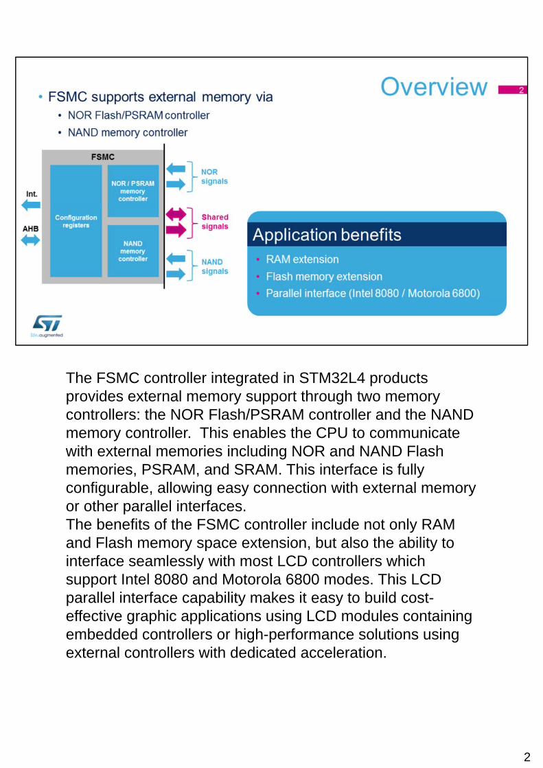
The FSMC controller integrated in STM32L4 products provides external memory support through two memory controllers: the NOR Flash/PSRAM controller and the NAND memory controller. This enables the CPU to communicate with external memories including NOR and NAND Flash memories, PSRAM, and SRAM. This interface is fully configurable, allowing easy connection with external memory or other parallel interfaces.The benefits of the FSMC controller include not only RAM and Flash memory space extension, but also the ability to interface seamlessly with most LCD controllers which support Intel 8080 and Motorola 6800 modes. This LCD parallel interface capability makes it easy to build cost-effective graphic applications using LCD modules containing embedded controllers or high-performance solutions using external controllers with dedicated acceleration.
2
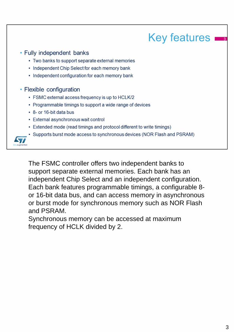
The FSMC controller offers two independent banks to support separate external memories. Each bank has an independent Chip Select and an independent configuration.Each bank features programmable timings, a configurable 8-or 16-bit data bus, and can access memory in asynchronous or burst mode for synchronous memory such as NOR Flash and PSRAM. Synchronous memory can be accessed at maximum frequency of HCLK divided by 2.
3
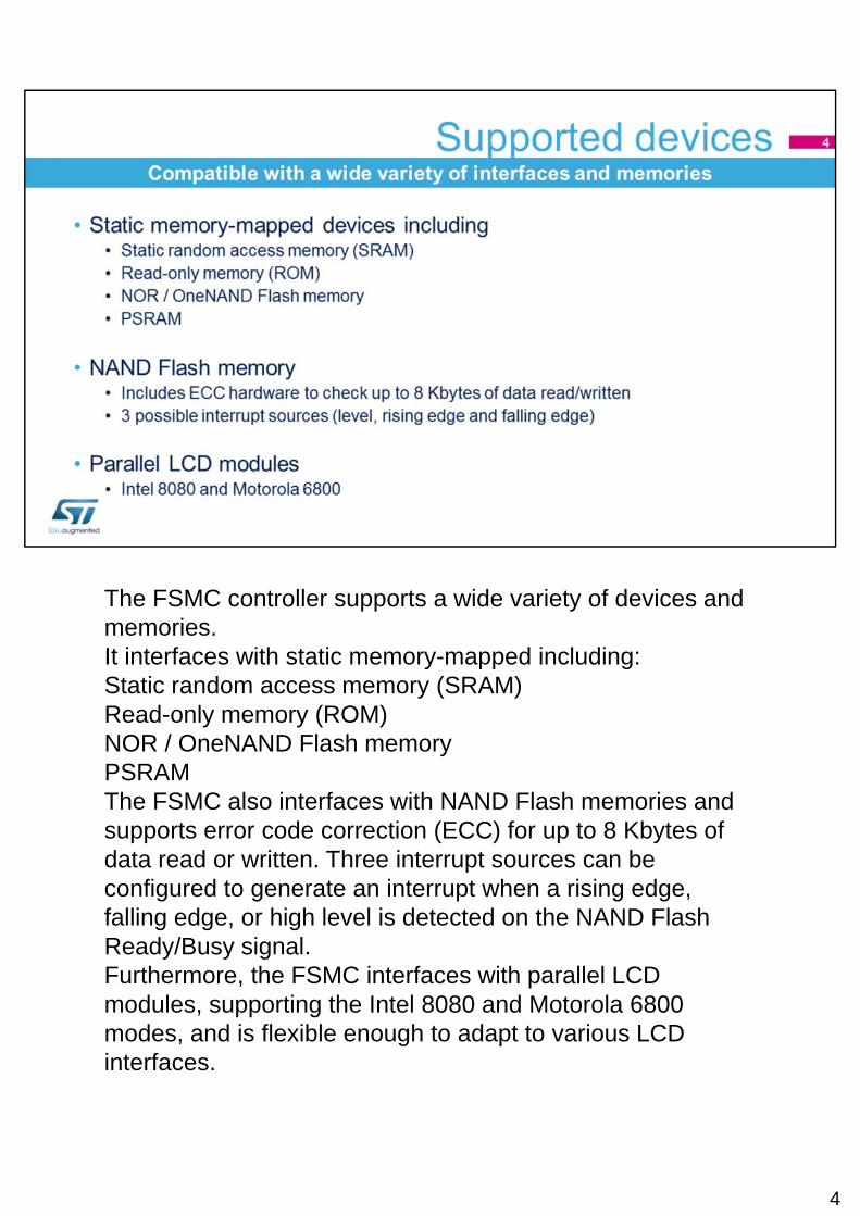
The FSMC controller supports a wide variety of devices and memories.It interfaces with static memory-mapped including:Static random access memory (SRAM)Read-only memory (ROM)NOR / OneNAND Flash memoryPSRAMThe FSMC also interfaces with NAND Flash memories and supports error code correction (ECC) for up to 8 Kbytes of data read or written. Three interrupt sources can be configured to generate an interrupt when a rising edge, falling edge, or high level is detected on the NAND Flash Ready/Busy signal.Furthermore, the FSMC interfaces with parallel LCD modules, supporting the Intel 8080 and Motorola 6800 modes, and is flexible enough to adapt to various LCD interfaces.
4
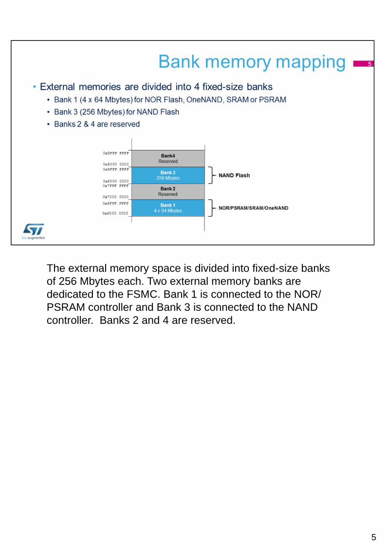
The external memory space is divided into fixed-size banks of 256 Mbytes each. Two external memory banks are dedicated to the FSMC. Bank 1 is connected to the NOR/ PSRAM controller and Bank 3 is connected to the NAND controller. Banks 2 and 4 are reserved.
5

Bank 1 is used to address up to 4 NOR Flash memories or PSRAM devices. This bank is split into 4 NOR or PSRAM sub-banks of 64 Mbytes each with 4 dedicated Chip Selects to interface with:8 or 16-bit synchronous or asynchronous NOR Flash in multiplexed or non-multiplexed mode.8 or 16-bit asynchronous SRAM and ROM.8 or 16-bit synchronous or asynchronous PSRAM memories.
6

The FSMC outputs a unique Chip Select signal to each bank and performs only one access at a time to an external device. The external memories are connected either to the NOR PSRAM controller or the NAND controller, and share address, data, and control signals.
7

The NOR PSRAM controller allows configuration of various timing parameters for the supported memories:Address setup phase: Duration of the first access phaseAddress hold phase: Duration of the middle phase of the access cycleData setup phase: Duration of the second access phaseBus turnaround phase: Duration of the bus turnaround phaseClock divide ratio: Number of AHB clock cycles (HCLK) within one memory clock cycle (CLK)Data latency: Number of clock cycles to be issued to the memory before the first data transferAccess mode.
8
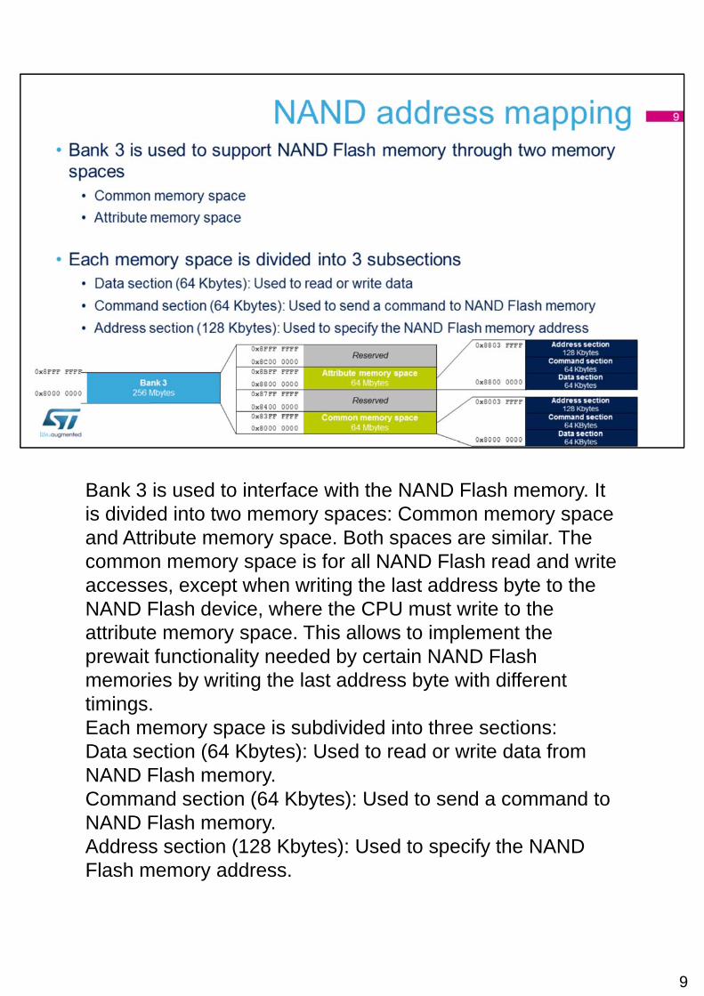
Bank 3 is used to interface with the NAND Flash memory. It is divided into two memory spaces: Common memory space and Attribute memory space. Both spaces are similar. The common memory space is for all NAND Flash read and write accesses, except when writing the last address byte to the NAND Flash device, where the CPU must write to the attribute memory space. This allows to implement the prewait functionality needed by certain NAND Flash memories by writing the last address byte with different timings.Each memory space is subdivided into three sections:Data section (64 Kbytes): Used to read or write data from NAND Flash memory.Command section (64 Kbytes): Used to send a command to NAND Flash memory.Address section (128 Kbytes): Used to specify the NAND Flash memory address.
9
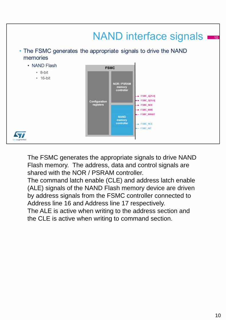
The FSMC generates the appropriate signals to drive NAND Flash memory. The address, data and control signals are shared with the NOR / PSRAM controller.The command latch enable (CLE) and address latch enable (ALE) signals of the NAND Flash memory device are driven by address signals from the FSMC controller connected to Address line 16 and Address line 17 respectively. The ALE is active when writing to the address section and the CLE is active when writing to command section.
10
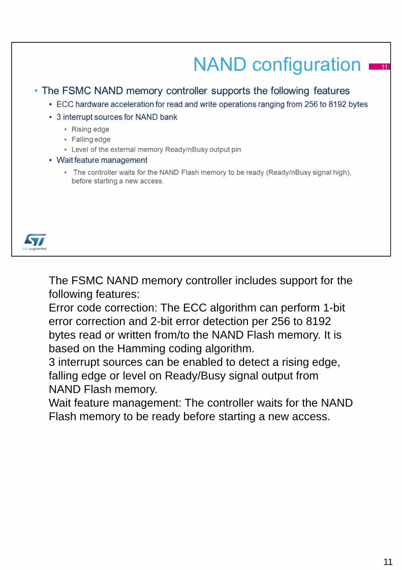
The FSMC NAND memory controller includes support for the following features:Error code correction: The ECC algorithm can perform 1-bit error correction and 2-bit error detection per 256 to 8192 bytes read or written from/to the NAND Flash memory. It is based on the Hamming coding algorithm.3 interrupt sources can be enabled to detect a rising edge, falling edge or level on Ready/Busy signal output from NAND Flash memory.Wait feature management: The controller waits for the NAND Flash memory to be ready before starting a new access.
11
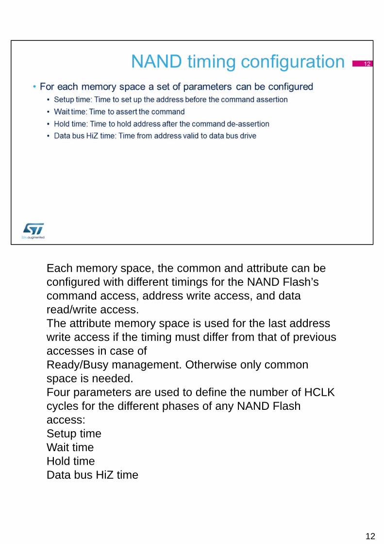
Each memory space, the common and attribute can be configured with different timings for the NAND Flash’s command access, address write access, and data read/write access.The attribute memory space is used for the last address write access if the timing must differ from that of previous accesses in case ofReady/Busy management. Otherwise only common space is needed.Four parameters are used to define the number of HCLK cycles for the different phases of any NAND Flash access:Setup timeWait timeHold timeData bus HiZ time
12

The NAND controller offers 3 interrupt sources: rising edge, falling edge, and high level detection on the FSMC INT pin when it is connected to the Ready/Busy signal from the NAND Flash memory.

The FSMC is active in Run, Sleep, Low-power run and Low-power sleep modes. A FSMC interrupt can cause the device to exit Sleep or Low-power sleep mode. In Stop 0, Stop 1 or Stop 2 mode, the FSMC is frozen, and the content of its registers is kept. In Standby or Shutdown mode, the FSMC is powered-down and it must be reinitialized afterwards.

Wearable applications require low-power management together with a high-quality user interface. This can be achieved using the STM32L4 FSMC to connect the display thanks to its flexibility and widely programmable parameters to interface with LCD modules. In addition the FSMC or Quad-SPI interface may be used may be used to access an external Flash memory containing all of the graphical content needed such as such as background images, high-resolution icons, or fonts to support multiple languages. Additional audio data for ringtones can also benefit from the large space offered by the external Flash memory.
Thank you.
15