hardware slides 15
TRANSCRIPT

8/3/2019 Hardware Slides 15
http://slidepdf.com/reader/full/hardware-slides-15 1/33
DOC 112: Computer Hardware Lecture 15 Slide 1
Lecture 15:
A Manual Processor (part 2)
8/3/2019 Hardware Slides 15
http://slidepdf.com/reader/full/hardware-slides-15 2/33
DOC 112: Computer Hardware Lecture 15 Slide 2
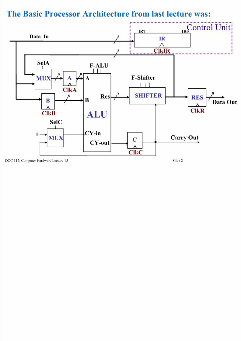
The Basic Processor Architecture from last lecture was:
SHIFTER
ALU
A
B
CY-in
CY-out
Res
MUX
1
IR7
Data In
Carry Out
Data Out
8
F-ALU
F-Shifter
SelA
SelC
RES
C
B
A
IR0
IR
MUX
8
8
8
8
8 8
ClkA
ClkB ClkR
ClkC
Control Unit
ClkIR

8/3/2019 Hardware Slides 15
http://slidepdf.com/reader/full/hardware-slides-15 3/33
DOC 112: Computer Hardware Lecture 15 Slide 3
Registers A B Res and IR are all of the form:
Register C is a single D-Q flip-flop

8/3/2019 Hardware Slides 15
http://slidepdf.com/reader/full/hardware-slides-15 4/33
DOC 112: Computer Hardware Lecture 15 Slide 4
Multiplexer to select A has the form:
Select
MUX
O7I7 0
1
O0I0 0
1
O1I1 0
1
The multiplexer to select Cis a single bit version of this
8/3/2019 Hardware Slides 15
http://slidepdf.com/reader/full/hardware-slides-15 5/33DOC 112: Computer Hardware Lecture 15 Slide 5
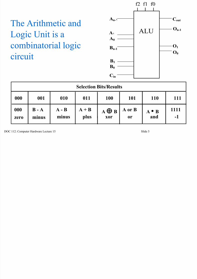
The Arithmetic and
Logic Unit is acombinatorial logic
circuit
f2 f1 f0
An-
A A0
Bn-1
B1
B0 Cin
On-1
Cout
O0
O1
ALU
Selection Bits/Results
000 001 010 011 100 101 110 111
000 A - B A B 1111
zero minus plus xor or and -1
A or B A • BB - A A + B
minus

8/3/2019 Hardware Slides 15
http://slidepdf.com/reader/full/hardware-slides-15 6/33DOC 112: Computer Hardware Lecture 15 Slide 6
The Shifter is another combinatorial logic circuit
implemented by multiplexers:
f2 f1 f0
In-1
I1I0
Cin
On-1
O0
O1
SHIFTER
8/3/2019 Hardware Slides 15
http://slidepdf.com/reader/full/hardware-slides-15 7/33DOC 112: Computer Hardware Lecture 15 Slide 7
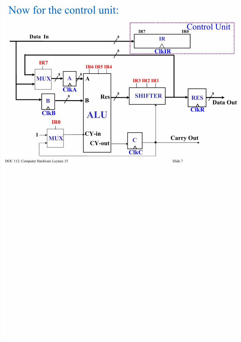
Now for the control unit:
SHIFTER
ALU
A
B
CY-in
CY-out
Res
MUX
1
IR7
Data In
Carry Out
Data Out
8
IR6 IR5 IR4
IR3 IR2 IR1
IR7
IR0
RES
C
B
A
IR0
IR
MUX
8
8
8
8
8 8
ClkA
ClkBClkR
ClkC
Control Unit
ClkIR

8/3/2019 Hardware Slides 15
http://slidepdf.com/reader/full/hardware-slides-15 8/33
DOC 112: Computer Hardware Lecture 15 Slide 8
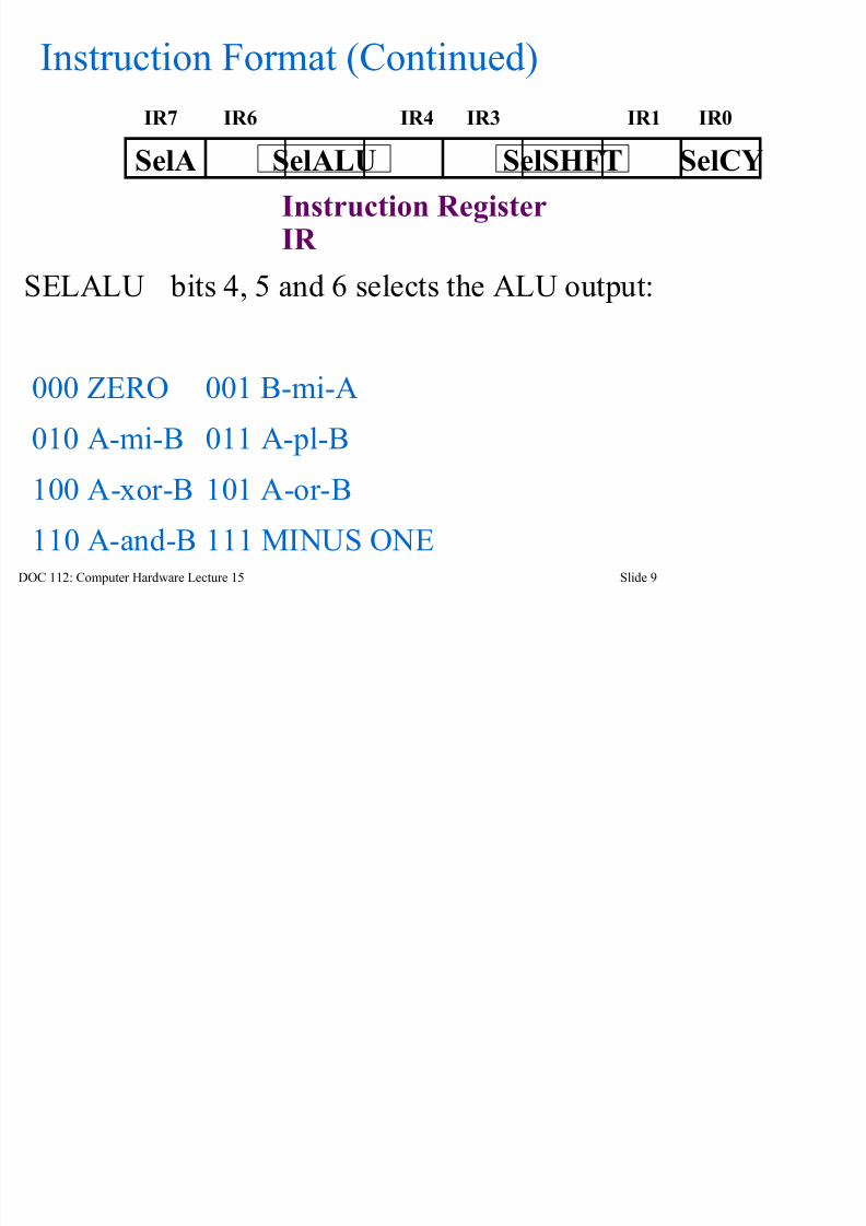
Instruction Format
The multiplexers are controlled by bits 0 and 7 of the instruction
SELA 0-1Selects the input to the A register0 selects shifter output, 1 selects external Data Input.
SELCY 0-1 Selects the input to the CARRY-in of the ALU: 0 selects logic 1, 1 selects C-out
Instruction Register IR
IR7 IR6 IR4 IR1 IR0IR3
SelA SelALU SelSHFT SelCY
8/3/2019 Hardware Slides 15
http://slidepdf.com/reader/full/hardware-slides-15 9/33
DOC 112: Computer Hardware Lecture 15 Slide 9
Instruction Format (Continued)
SELALU bits 4, 5 and 6 selects the ALU output:
000 ZERO 001 B-mi-A
010 A-mi-B 011 A-pl-B100 A-xor-B 101 A-or-B
110 A-and-B 111 MINUS ONE
Instruction RegisterIR
IR7 IR6 IR4 IR1 IR0IR3
SelA SelALU SelSHFT SelCY

8/3/2019 Hardware Slides 15
http://slidepdf.com/reader/full/hardware-slides-15 10/33
DOC 112: Computer Hardware Lecture 15 Slide 10
Instruction Format (Continued)
SELSHIFTSelects the shift function:000: Unchanged 001: Arithmetic Left Shift
010: Rotate Right 011: Logical right shift
100: Unchanged 101: Left shift with carry
110: Arithmetic right shift 111: Right shift with carry
Instruction Register IR
IR7 IR6 IR4 IR1 IR0IR3
SelA SelALU SelSHFT SelCY

8/3/2019 Hardware Slides 15
http://slidepdf.com/reader/full/hardware-slides-15 11/33
DOC 112: Computer Hardware Lecture 15 Slide 11
Designing the control unit
OPERATE
CONTROL
System Clock
ClkIR
ClkA
ClkB
ClkR
ClkC
At each clock pulsethe controller
provides one or moreregister with a clock
pulse taking the processor through afixed cycle of states

8/3/2019 Hardware Slides 15
http://slidepdf.com/reader/full/hardware-slides-15 12/33
DOC 112: Computer Hardware Lecture 15 Slide 12
Execution Cycle of the Manual Processor
1. Load the "Data In" lines into the IR register.
2. Load the A register
3. Load the B and the C registers
4. Load the "Data In" lines into the IR register
5. Load the RES and the C registers
.... Go to step 1 of the next instruction ....

8/3/2019 Hardware Slides 15
http://slidepdf.com/reader/full/hardware-slides-15 13/33
DOC 112: Computer Hardware Lecture 15 Slide 13
The State Transition Diagram

8/3/2019 Hardware Slides 15
http://slidepdf.com/reader/full/hardware-slides-15 14/33
DOC 112: Computer Hardware Lecture 15 Slide 14
The Program
Operation Code 1
Data 1
Data 2Operation Code 2
Unused
Instruction
Instruction
Instruction
etc.
The execution cycleimplicitly defines the
format of the program.
At each step a new item
arrives on the data in
lines synchronised with
the system clock.

8/3/2019 Hardware Slides 15
http://slidepdf.com/reader/full/hardware-slides-15 15/33
DOC 112: Computer Hardware Lecture 15 Slide 15
The processing cycle
SHIFTER
ALU
A
B
CY-in
CY-out
Res
MUX
1
IR7
Data In
Carry Out
Data Out
8
IR6 IR5 IR4
IR3 IR2 IR1
IR7
IR0
RES
C
B
A
IR0
IR
MUX
8
8
8
8
8 8
ClkA
ClkBClkR
ClkC
Control Unit
ClkIR
Step 1: IR receives a clock

8/3/2019 Hardware Slides 15
http://slidepdf.com/reader/full/hardware-slides-15 16/33
DOC 112: Computer Hardware Lecture 15 Slide 16
SHIFTER
ALU
A
B
CY-in
CY-out
Res
MUX
1
IR7
Data In
Carry Out
Data Out
8
IR6 IR5 IR4
IR3 IR2 IR1
IR7
IR0
RES
C
B
A
IR0
IR
MUX
8
8
8
8
8 8
ClkA
ClkBClkR
ClkC
Control Unit
ClkIR
Step 1: IR receives a clock pulse. It is loaded from theData In lines
Step 2: A receives a clock

8/3/2019 Hardware Slides 15
http://slidepdf.com/reader/full/hardware-slides-15 17/33
DOC 112: Computer Hardware Lecture 15 Slide 17
SHIFTER
ALU
A
B
CY-in
CY-out
Res
MUX
1
IR7
Data In
Carry Out
Data Out
8
IR6 IR5 IR4
IR3 IR2 IR1
IR7
IR0
RES
C
B
A
IR0
IR
MUX
8
8
8
8
8 8
ClkA
ClkBClkR
ClkC
Control Unit
ClkIR
Step 2: A receives a clock pulse. It might be loaded fromthe Data In lines
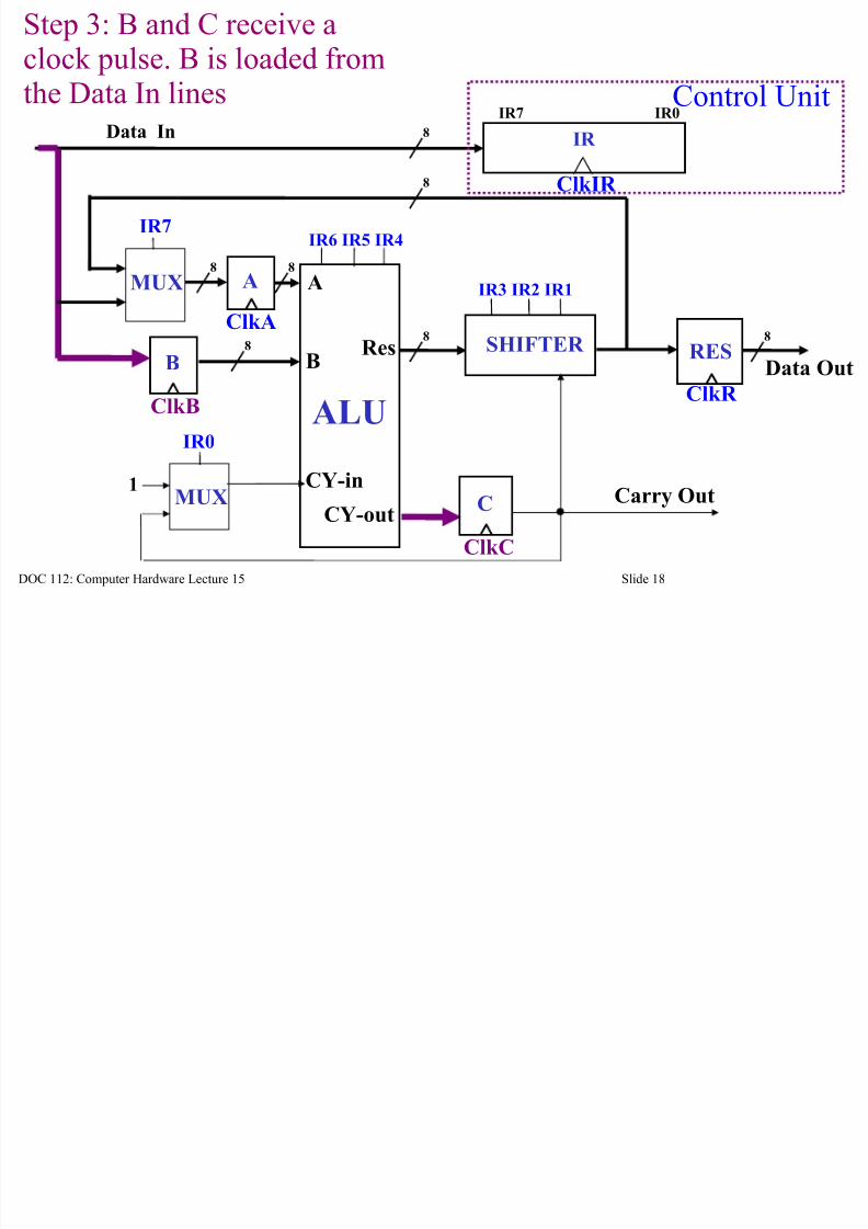
Step 3: B and C receive a
8/3/2019 Hardware Slides 15
http://slidepdf.com/reader/full/hardware-slides-15 18/33
DOC 112: Computer Hardware Lecture 15 Slide 18
SHIFTER
ALU
A
B
CY-in
CY-out
Res
MUX
1
IR7
Data In
Carry Out
Data Out
8
IR6 IR5 IR4
IR3 IR2 IR1
IR7
IR0
RES
C
B
A
IR0
IR
MUX
8
8
8
8
8 8
ClkA
ClkBClkR
ClkC
Control Unit
ClkIR
Step 3: B and C receive aclock pulse. B is loaded fromthe Data In lines
Step 4: IR receives a clock

8/3/2019 Hardware Slides 15
http://slidepdf.com/reader/full/hardware-slides-15 19/33
DOC 112: Computer Hardware Lecture 15 Slide 19
SHIFTER
ALU
A
B
CY-in
CY-out
Res
MUX
1
IR7
Data In
Carry Out
Data Out
8
IR6 IR5 IR4
IR3 IR2 IR1
IR7
IR0
RES
C
B
A
IR0
IR
MUX
8
8
8
8
8 8
ClkA
ClkBClkR
ClkC
Control Unit
ClkIR
Step 4: IR receives a clock pulse. It is loaded from theData In lines
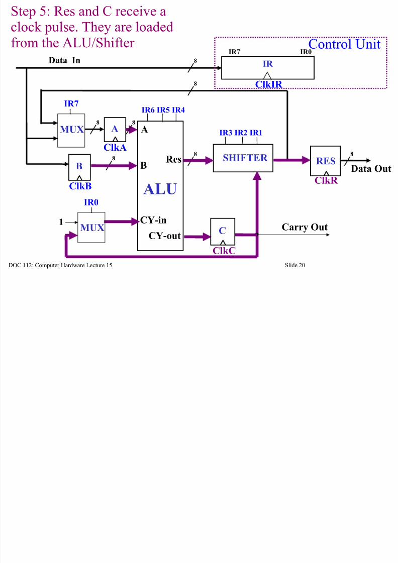
Step 5: Res and C receive a
8/3/2019 Hardware Slides 15
http://slidepdf.com/reader/full/hardware-slides-15 20/33
DOC 112: Computer Hardware Lecture 15 Slide 20
SHIFTER
ALU
A
B
CY-in
CY-out
Res
MUX
1
IR7
Data In
Carry Out
Data Out
8
IR6 IR5 IR4
IR3 IR2 IR1
IR7
IR0
RES
C
B
A
IR0
IR
MUX
8
8
8
8
8 8
ClkA
ClkBClkR
ClkC
Control Unit
ClkIR
Step 5: Res and C receive aclock pulse. They are loadedfrom the ALU/Shifter
Step 1 (again): IR receives a

8/3/2019 Hardware Slides 15
http://slidepdf.com/reader/full/hardware-slides-15 21/33
DOC 112: Computer Hardware Lecture 15 Slide 21
SHIFTER
ALU
A
B
CY-in
CY-out
Res
MUX
1
IR7
Data In
Carry Out
Data Out
8
IR6 IR5 IR4
IR3 IR2 IR1
IR7
IR0
RES
C
B
A
IR0
IR
MUX
8
8
8
8
8 8
ClkA
ClkBClkR
ClkC
Control Unit
ClkIR
Step 1 (again): IR receives aclock pulse. It is loaded fromthe Data In lines
Step 2 (again): A receives a

8/3/2019 Hardware Slides 15
http://slidepdf.com/reader/full/hardware-slides-15 22/33
DOC 112: Computer Hardware Lecture 15 Slide 22
SHIFTER
ALU
A
B
CY-in
CY-out
Res
MUX
1
IR7
Data In
Carry Out
Data Out
8
IR6 IR5 IR4
IR3 IR2 IR1
IR7
IR0
RES
C
B
A
IR0
IR
MUX
8
8
8
8
8 8
ClkA
ClkBClkR
ClkC
Control Unit
ClkIR
Step 2 (again): A receives aclock pulse. It might beloaded from the ALU/Shifter

8/3/2019 Hardware Slides 15
http://slidepdf.com/reader/full/hardware-slides-15 23/33
DOC 112: Computer Hardware Lecture 15 Slide 23
The cycle continues
The cycle continues in the same way while the processor is being operated, taking data andinstructions from the Data In lines and putting theresults on the Data Out lines.
The design of the control unit which implementsthis cycle follows our (now very familiar)methodology.
8/3/2019 Hardware Slides 15
http://slidepdf.com/reader/full/hardware-slides-15 24/33
DOC 112: Computer Hardware Lecture 15 Slide 24
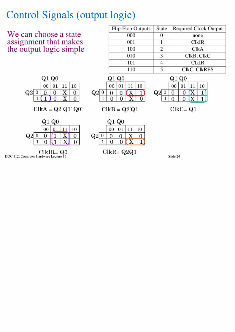
Control Signals (output logic)
We can choose a state
assignment that makesthe output logic simple
h i i bl
8/3/2019 Hardware Slides 15
http://slidepdf.com/reader/full/hardware-slides-15 25/33
DOC 112: Computer Hardware Lecture 15 Slide 25
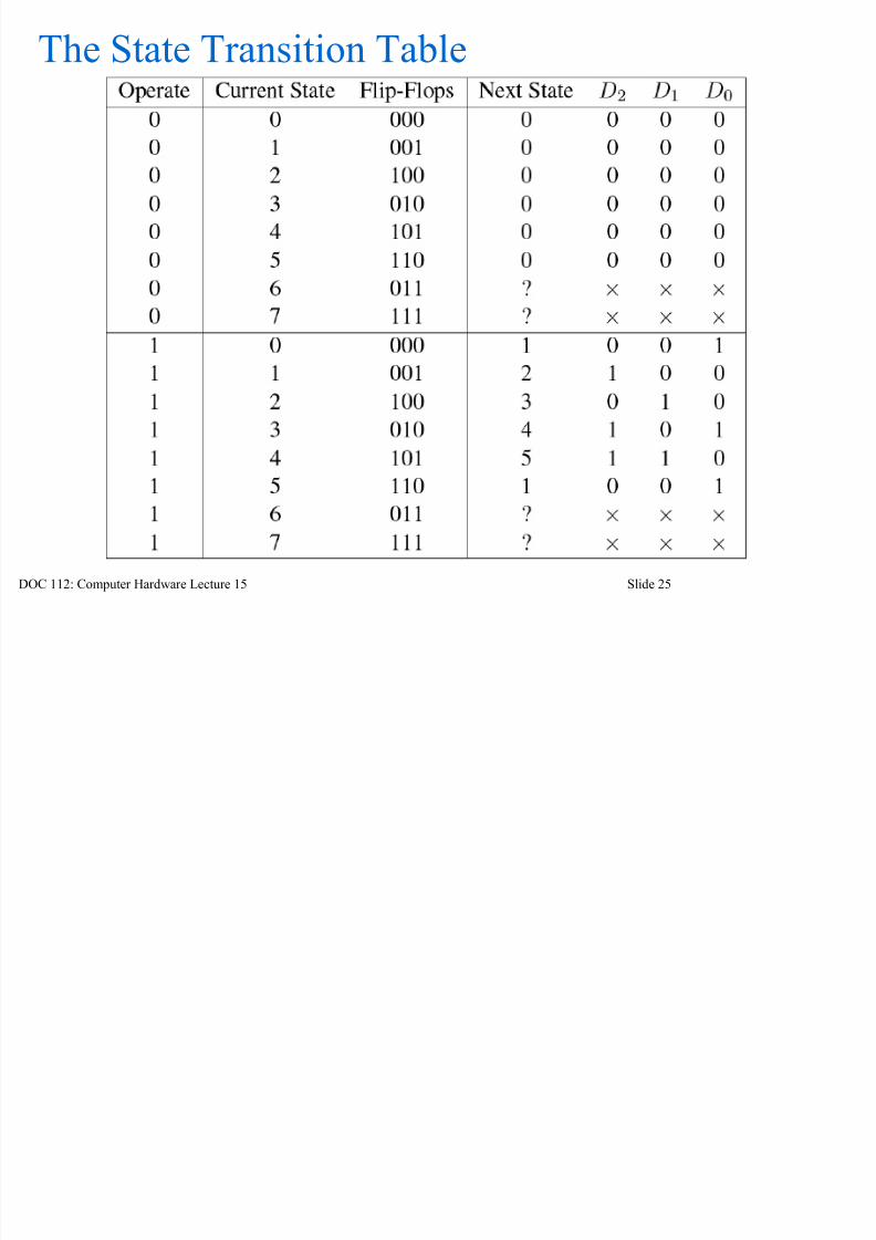
The State Transition Table

8/3/2019 Hardware Slides 15
http://slidepdf.com/reader/full/hardware-slides-15 26/33
DOC 112: Computer Hardware Lecture 15 Slide 26
Karnaugh Maps of the Controller
8/3/2019 Hardware Slides 15
http://slidepdf.com/reader/full/hardware-slides-15 27/33
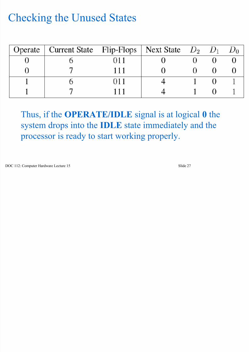
DOC 112: Computer Hardware Lecture 15 Slide 27
Checking the Unused States
Thus, if the OPERATE/IDLE signal is at logical 0 the
system drops into the IDLE state immediately and the
processor is ready to start working properly.
8/3/2019 Hardware Slides 15
http://slidepdf.com/reader/full/hardware-slides-15 28/33
DOC 112: Computer Hardware Lecture 15 Slide 28
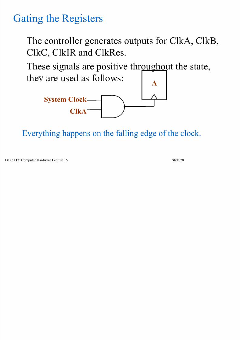
Gating the Registers
The controller generates outputs for ClkA, ClkB,ClkC, ClkIR and ClkRes.
These signals are positive throughout the state,
the are used as follows:
Everything happens on the falling edge of the clock.
A
System Clock
ClkA

8/3/2019 Hardware Slides 15
http://slidepdf.com/reader/full/hardware-slides-15 29/33
DOC 112: Computer Hardware Lecture 15 Slide 29
Gating the Registers
A safer design has the controller changing on the negative edge
and the registers being loaded on the positive edge of the clock.
This ensures that, when the input is taken from the RAM it can
be properly established before a register is loaded.
A NAND gate does the trick
A
System Clock
ClkA

8/3/2019 Hardware Slides 15
http://slidepdf.com/reader/full/hardware-slides-15 30/33
DOC 112: Computer Hardware Lecture 15 Slide 30
Program Execution: Compute (A+B)/2
The processor is in theIDLE state
0.Set OPERATE/IDLE signal to 0 &apply two clocks.
1. Set OPERATE/IDLE to 1
Set input data to 10000000 &apply one clock pulse.
2. Set number A on the Data
In lines & apply one clock
pulse
Input is loaded in the IR
register. ALU is set to00000000, shifter =
unchanged.
Because IR7=1 the Data Inlines are loaded onto
register A.

8/3/2019 Hardware Slides 15
http://slidepdf.com/reader/full/hardware-slides-15 31/33
DOC 112: Computer Hardware Lecture 15 Slide 31
Program Execution: (A+B)/2
3.Set number B on the Data In
lines and apply one clock pulseB is loaded from the Data In lines
and C is loaded from the ALU
carry which is 0
4. Set the Data In lines toto 00110111 and apply
one clock pulse.
5. Apply one clock pulse.
The IR register is loaded from theData In line. The ALU is set to A
plus B and the shifter to logical
shift right.
The result (A+B)/2 is clocked intothe RES register, the C bit
indicates overflow

8/3/2019 Hardware Slides 15
http://slidepdf.com/reader/full/hardware-slides-15 32/33
DOC 112: Computer Hardware Lecture 15 Slide 32
The (A+B)/2 instruction in a program
The decrement instruction
could be used as part of a
longer program.
The result of decrementingthe number goes back to
memory via the data out
lines
Instruction
10000000
Number A
Number B
00110111 Unused
Instruction
Instruction

8/3/2019 Hardware Slides 15
http://slidepdf.com/reader/full/hardware-slides-15 33/33
DOC 112: Computer Hardware Lecture 15 Slide 33
At last:
We have succeeded in executing one program instruction!
We’ll take a look at getting the instructions in and the results out
next time.