hardcopy iii device handbook - intel...iv contents hardcopy iii device handbook volume 1: device...
TRANSCRIPT
101 Innovation DriveSan Jose, CA 95134www.altera.com
HC3_H5V1-3.4
Volume 1: Device Interfaces and Integration
HardCopy III Device Handbook
HardCopy III Device Handbook Volume 1: Device Interfaces and Integration

HardCopy III Device Handbook Volume 1: Device Interfaces and Integration March 2012 Altera Corporation
© 2012 Altera Corporation. All rights reserved. ALTERA, ARRIA, CYCLONE, HARDCOPY, MAX, MEGACORE, NIOS, QUARTUS and STRATIX are Reg. U.S. Pat.& Tm. Off. and/or trademarks of Altera Corporation in the U.S. and other countries. All other trademarks and service marks are the property of their respectiveholders as described at www.altera.com/common/legal.html. Altera warrants performance of its semiconductor products to current specifications in accordancewith Altera’s standard warranty, but reserves the right to make changes to any products and services at any time without notice. Altera assumes no responsibility orliability arising out of the application or use of any information, product, or service described herein except as expressly agreed to in writing by Altera. Alteracustomers are advised to obtain the latest version of device specifications before relying on any published information and before placing orders for products orservices.
March 2012 Altera Corporation HardCopy III Device Handbook Volume 1: Device Interfaces and Integration
Contents
Section I. Device Core
Chapter 1. HardCopy III Device Family OverviewFeatures . . . . . . . . . . . . . . . . . . . . . . . . . . . . . . . . . . . . . . . . . . . . . . . . . . . . . . . . . . . . . . . . . . . . . . . . . . . . . . . . 1–2
HardCopy III ASIC and Stratix III FPGA Mapping Paths . . . . . . . . . . . . . . . . . . . . . . . . . . . . . . . . . . . 1–4HardCopy III Package Pro . . . . . . . . . . . . . . . . . . . . . . . . . . . . . . . . . . . . . . . . . . . . . . . . . . . . . . . . . . . . . 1–7Differences Between HardCopy III and Stratix III Devices . . . . . . . . . . . . . . . . . . . . . . . . . . . . . . . . . . 1–8
Architectural Features . . . . . . . . . . . . . . . . . . . . . . . . . . . . . . . . . . . . . . . . . . . . . . . . . . . . . . . . . . . . . . . . . . . 1–9Logic Array Block and Adaptive Logic Module Function Support . . . . . . . . . . . . . . . . . . . . . . . . . . . 1–9DSP Function Support . . . . . . . . . . . . . . . . . . . . . . . . . . . . . . . . . . . . . . . . . . . . . . . . . . . . . . . . . . . . . . . . . 1–9TriMatrix Embedded Memory Blocks . . . . . . . . . . . . . . . . . . . . . . . . . . . . . . . . . . . . . . . . . . . . . . . . . . . 1–10Clock Networks and PLLs . . . . . . . . . . . . . . . . . . . . . . . . . . . . . . . . . . . . . . . . . . . . . . . . . . . . . . . . . . . . . 1–10I/O Banks and I/O Structure . . . . . . . . . . . . . . . . . . . . . . . . . . . . . . . . . . . . . . . . . . . . . . . . . . . . . . . . . . 1–11External Memory Interfaces . . . . . . . . . . . . . . . . . . . . . . . . . . . . . . . . . . . . . . . . . . . . . . . . . . . . . . . . . . . 1–11High-Speed Differential I/O Interfaces with DPA . . . . . . . . . . . . . . . . . . . . . . . . . . . . . . . . . . . . . . . . 1–11Hot Socketing and Power-On Reset . . . . . . . . . . . . . . . . . . . . . . . . . . . . . . . . . . . . . . . . . . . . . . . . . . . . . 1–12IEEE 1149.1 (JTAG) Boundary Scan Testing . . . . . . . . . . . . . . . . . . . . . . . . . . . . . . . . . . . . . . . . . . . . . . 1–13Signal Integrity . . . . . . . . . . . . . . . . . . . . . . . . . . . . . . . . . . . . . . . . . . . . . . . . . . . . . . . . . . . . . . . . . . . . . . 1–13
Software Support and Part Number Information . . . . . . . . . . . . . . . . . . . . . . . . . . . . . . . . . . . . . . . . . . . 1–13Software Support . . . . . . . . . . . . . . . . . . . . . . . . . . . . . . . . . . . . . . . . . . . . . . . . . . . . . . . . . . . . . . . . . . . . 1–14Part Number Information . . . . . . . . . . . . . . . . . . . . . . . . . . . . . . . . . . . . . . . . . . . . . . . . . . . . . . . . . . . . . 1–14
Document Revision History . . . . . . . . . . . . . . . . . . . . . . . . . . . . . . . . . . . . . . . . . . . . . . . . . . . . . . . . . . . . . 1–15
Chapter 2. Logic Array Block and Adaptive Logic Module Implementation in HardCopy III DevicesHCells . . . . . . . . . . . . . . . . . . . . . . . . . . . . . . . . . . . . . . . . . . . . . . . . . . . . . . . . . . . . . . . . . . . . . . . . . . . . . . . . . 2–1ALM and LAB Function Implementation . . . . . . . . . . . . . . . . . . . . . . . . . . . . . . . . . . . . . . . . . . . . . . . . . . . 2–2MLAB Function Implementation . . . . . . . . . . . . . . . . . . . . . . . . . . . . . . . . . . . . . . . . . . . . . . . . . . . . . . . . . . 2–4Document Revision History . . . . . . . . . . . . . . . . . . . . . . . . . . . . . . . . . . . . . . . . . . . . . . . . . . . . . . . . . . . . . . 2–4
Chapter 3. DSP Block Implementation in HardCopy III DevicesDSP Function Implementation . . . . . . . . . . . . . . . . . . . . . . . . . . . . . . . . . . . . . . . . . . . . . . . . . . . . . . . . . . . . 3–1DSP Operational Mode and Feature Support . . . . . . . . . . . . . . . . . . . . . . . . . . . . . . . . . . . . . . . . . . . . . . . . 3–3Document Revision History . . . . . . . . . . . . . . . . . . . . . . . . . . . . . . . . . . . . . . . . . . . . . . . . . . . . . . . . . . . . . . 3–3
Chapter 4. TriMatrix Embedded Memory Blocks in HardCopy III DevicesMemory Resources and Features . . . . . . . . . . . . . . . . . . . . . . . . . . . . . . . . . . . . . . . . . . . . . . . . . . . . . . . . . . 4–1
MLAB Implementation . . . . . . . . . . . . . . . . . . . . . . . . . . . . . . . . . . . . . . . . . . . . . . . . . . . . . . . . . . . . . . . . 4–3Design Considerations . . . . . . . . . . . . . . . . . . . . . . . . . . . . . . . . . . . . . . . . . . . . . . . . . . . . . . . . . . . . . . . . . . . 4–4Document Revision History . . . . . . . . . . . . . . . . . . . . . . . . . . . . . . . . . . . . . . . . . . . . . . . . . . . . . . . . . . . . . . 4–4
Chapter 5. Clock Networks and PLLs in HardCopy III DevicesClock Networks in HardCopy III Devices . . . . . . . . . . . . . . . . . . . . . . . . . . . . . . . . . . . . . . . . . . . . . . . . . . . 5–1
Clock Network Resources . . . . . . . . . . . . . . . . . . . . . . . . . . . . . . . . . . . . . . . . . . . . . . . . . . . . . . . . . . . . . . 5–1Clocking Regions . . . . . . . . . . . . . . . . . . . . . . . . . . . . . . . . . . . . . . . . . . . . . . . . . . . . . . . . . . . . . . . . . . . . . 5–3Clock Control Block . . . . . . . . . . . . . . . . . . . . . . . . . . . . . . . . . . . . . . . . . . . . . . . . . . . . . . . . . . . . . . . . . . . 5–3
PLLs in HardCopy III Devices . . . . . . . . . . . . . . . . . . . . . . . . . . . . . . . . . . . . . . . . . . . . . . . . . . . . . . . . . . . . . 5–3Design Considerations . . . . . . . . . . . . . . . . . . . . . . . . . . . . . . . . . . . . . . . . . . . . . . . . . . . . . . . . . . . . . . . . . . . 5–6Document Revision History . . . . . . . . . . . . . . . . . . . . . . . . . . . . . . . . . . . . . . . . . . . . . . . . . . . . . . . . . . . . . . 5–8

iv Contents
HardCopy III Device Handbook Volume 1: Device Interfaces and Integration March 2012 Altera Corporation
Section II. I/O Interfaces
Chapter 6. I/O Features for HardCopy III DevicesDifferences Between HardCopy III ASICs and Stratix III FPGAs . . . . . . . . . . . . . . . . . . . . . . . . . . . . . . . 6–2I/O Standards and Voltage Levels . . . . . . . . . . . . . . . . . . . . . . . . . . . . . . . . . . . . . . . . . . . . . . . . . . . . . . . . . 6–4HardCopy III I/O . . . . . . . . . . . . . . . . . . . . . . . . . . . . . . . . . . . . . . . . . . . . . . . . . . . . . . . . . . . . . . . . . . . . . . . 6–7HardCopy III I/O Banks . . . . . . . . . . . . . . . . . . . . . . . . . . . . . . . . . . . . . . . . . . . . . . . . . . . . . . . . . . . . . . . . . 6–8HardCopy III I/O Structure . . . . . . . . . . . . . . . . . . . . . . . . . . . . . . . . . . . . . . . . . . . . . . . . . . . . . . . . . . . . . . . 6–9MultiVolt I/O Interface . . . . . . . . . . . . . . . . . . . . . . . . . . . . . . . . . . . . . . . . . . . . . . . . . . . . . . . . . . . . . . . . . . 6–93.3/3.0-V I/O Interface . . . . . . . . . . . . . . . . . . . . . . . . . . . . . . . . . . . . . . . . . . . . . . . . . . . . . . . . . . . . . . . . . . 6–10On-Chip Termination Support and I/O Termination Schemes . . . . . . . . . . . . . . . . . . . . . . . . . . . . . . . . 6–11OCT Calibration Block Location . . . . . . . . . . . . . . . . . . . . . . . . . . . . . . . . . . . . . . . . . . . . . . . . . . . . . . . . . . 6–12Design Considerations . . . . . . . . . . . . . . . . . . . . . . . . . . . . . . . . . . . . . . . . . . . . . . . . . . . . . . . . . . . . . . . . . . 6–12
I/O Banks Restrictions . . . . . . . . . . . . . . . . . . . . . . . . . . . . . . . . . . . . . . . . . . . . . . . . . . . . . . . . . . . . . . . . 6–12Non-Voltage-Referenced Standards . . . . . . . . . . . . . . . . . . . . . . . . . . . . . . . . . . . . . . . . . . . . . . . . . . . . 6–13Voltage-Referenced Standards . . . . . . . . . . . . . . . . . . . . . . . . . . . . . . . . . . . . . . . . . . . . . . . . . . . . . . . . . 6–13Mixing Voltage-Referenced and Non-Voltage-Referenced Standards . . . . . . . . . . . . . . . . . . . . . . . . 6–13Non-Socket Replacement and I/O Resource Availability . . . . . . . . . . . . . . . . . . . . . . . . . . . . . . . . . . 6–13
Document Revision History . . . . . . . . . . . . . . . . . . . . . . . . . . . . . . . . . . . . . . . . . . . . . . . . . . . . . . . . . . . . . 6–14
Chapter 7. External Memory Interfaces in HardCopy III DevicesMemory Interfaces Pin Support . . . . . . . . . . . . . . . . . . . . . . . . . . . . . . . . . . . . . . . . . . . . . . . . . . . . . . . . . . . 7–3
Data and Data Clock/Strobe Pins . . . . . . . . . . . . . . . . . . . . . . . . . . . . . . . . . . . . . . . . . . . . . . . . . . . . . . . 7–4Optional Parity, DM, BWSn, ECC, and QVLD Pins . . . . . . . . . . . . . . . . . . . . . . . . . . . . . . . . . . . . . . . 7–13Address and Control/Command Pins . . . . . . . . . . . . . . . . . . . . . . . . . . . . . . . . . . . . . . . . . . . . . . . . . . 7–14Memory Clock Pins . . . . . . . . . . . . . . . . . . . . . . . . . . . . . . . . . . . . . . . . . . . . . . . . . . . . . . . . . . . . . . . . . . 7–14
HardCopy III External Memory Interface Features . . . . . . . . . . . . . . . . . . . . . . . . . . . . . . . . . . . . . . . . . . 7–15DQS Phase-Shift Circuitry . . . . . . . . . . . . . . . . . . . . . . . . . . . . . . . . . . . . . . . . . . . . . . . . . . . . . . . . . . . . . 7–16
DLL . . . . . . . . . . . . . . . . . . . . . . . . . . . . . . . . . . . . . . . . . . . . . . . . . . . . . . . . . . . . . . . . . . . . . . . . . . . . . 7–17Phase Offset Control . . . . . . . . . . . . . . . . . . . . . . . . . . . . . . . . . . . . . . . . . . . . . . . . . . . . . . . . . . . . . . . 7–21DQS Logic Block . . . . . . . . . . . . . . . . . . . . . . . . . . . . . . . . . . . . . . . . . . . . . . . . . . . . . . . . . . . . . . . . . . 7–23DQS Delay Chain . . . . . . . . . . . . . . . . . . . . . . . . . . . . . . . . . . . . . . . . . . . . . . . . . . . . . . . . . . . . . . . . . . 7–23Update Enable Circuitry . . . . . . . . . . . . . . . . . . . . . . . . . . . . . . . . . . . . . . . . . . . . . . . . . . . . . . . . . . . . 7–24DQS Postamble Circuitry . . . . . . . . . . . . . . . . . . . . . . . . . . . . . . . . . . . . . . . . . . . . . . . . . . . . . . . . . . . 7–24
Leveling Circuitry . . . . . . . . . . . . . . . . . . . . . . . . . . . . . . . . . . . . . . . . . . . . . . . . . . . . . . . . . . . . . . . . . . . . 7–26Dynamic On-Chip Termination Control . . . . . . . . . . . . . . . . . . . . . . . . . . . . . . . . . . . . . . . . . . . . . . . . . 7–28I/O Element Registers . . . . . . . . . . . . . . . . . . . . . . . . . . . . . . . . . . . . . . . . . . . . . . . . . . . . . . . . . . . . . . . . 7–28IOE Features . . . . . . . . . . . . . . . . . . . . . . . . . . . . . . . . . . . . . . . . . . . . . . . . . . . . . . . . . . . . . . . . . . . . . . . . 7–31
OCT . . . . . . . . . . . . . . . . . . . . . . . . . . . . . . . . . . . . . . . . . . . . . . . . . . . . . . . . . . . . . . . . . . . . . . . . . . . . . 7–31IOE Delay Chains . . . . . . . . . . . . . . . . . . . . . . . . . . . . . . . . . . . . . . . . . . . . . . . . . . . . . . . . . . . . . . . . . . 7–31Output Buffer Delay . . . . . . . . . . . . . . . . . . . . . . . . . . . . . . . . . . . . . . . . . . . . . . . . . . . . . . . . . . . . . . . 7–32Slew Rate Control . . . . . . . . . . . . . . . . . . . . . . . . . . . . . . . . . . . . . . . . . . . . . . . . . . . . . . . . . . . . . . . . . 7–32Drive Strength . . . . . . . . . . . . . . . . . . . . . . . . . . . . . . . . . . . . . . . . . . . . . . . . . . . . . . . . . . . . . . . . . . . . 7–32
PLL . . . . . . . . . . . . . . . . . . . . . . . . . . . . . . . . . . . . . . . . . . . . . . . . . . . . . . . . . . . . . . . . . . . . . . . . . . . . . . . . 7–32Document Revision History . . . . . . . . . . . . . . . . . . . . . . . . . . . . . . . . . . . . . . . . . . . . . . . . . . . . . . . . . . . . . 7–33

Contents v
March 2012 Altera Corporation HardCopy III Device Handbook Volume 1: Device Interfaces and Integration
Chapter 8. High-Speed Differential I/O Interfaces and DPA in HardCopy III DevicesI/O Banks . . . . . . . . . . . . . . . . . . . . . . . . . . . . . . . . . . . . . . . . . . . . . . . . . . . . . . . . . . . . . . . . . . . . . . . . . . . . . . 8–2LVDS Channels . . . . . . . . . . . . . . . . . . . . . . . . . . . . . . . . . . . . . . . . . . . . . . . . . . . . . . . . . . . . . . . . . . . . . . . . . 8–3Differential Transmitter . . . . . . . . . . . . . . . . . . . . . . . . . . . . . . . . . . . . . . . . . . . . . . . . . . . . . . . . . . . . . . . . . . 8–4Differential Receiver . . . . . . . . . . . . . . . . . . . . . . . . . . . . . . . . . . . . . . . . . . . . . . . . . . . . . . . . . . . . . . . . . . . . . 8–6Receiver Data Realignment Circuit (Bit Slip) . . . . . . . . . . . . . . . . . . . . . . . . . . . . . . . . . . . . . . . . . . . . . . . . 8–7Dynamic Phase Aligner . . . . . . . . . . . . . . . . . . . . . . . . . . . . . . . . . . . . . . . . . . . . . . . . . . . . . . . . . . . . . . . . . . 8–8Soft-CDR Mode . . . . . . . . . . . . . . . . . . . . . . . . . . . . . . . . . . . . . . . . . . . . . . . . . . . . . . . . . . . . . . . . . . . . . . . . . 8–9Synchronizer . . . . . . . . . . . . . . . . . . . . . . . . . . . . . . . . . . . . . . . . . . . . . . . . . . . . . . . . . . . . . . . . . . . . . . . . . . 8–10Pre-Emphasis and Output Differential Voltage . . . . . . . . . . . . . . . . . . . . . . . . . . . . . . . . . . . . . . . . . . . . . 8–10Differential I/O Termination . . . . . . . . . . . . . . . . . . . . . . . . . . . . . . . . . . . . . . . . . . . . . . . . . . . . . . . . . . . . . 8–11Left and Right PLLs (PLL_Lx and PLL_Rx) . . . . . . . . . . . . . . . . . . . . . . . . . . . . . . . . . . . . . . . . . . . . . . . . 8–11Clocking . . . . . . . . . . . . . . . . . . . . . . . . . . . . . . . . . . . . . . . . . . . . . . . . . . . . . . . . . . . . . . . . . . . . . . . . . . . . . . 8–12High-Speed Differential I/O Interfaces and DPA in HardCopy III Devices Differential Data Orientation . . . . . . . . . . . . . . . . . . . . . . . . . . . . . . . . . . . . . . . . . . . . . . . . . . . . . . . . . . . . . . . . . . . . . . . . . . . . . . . . . . . . . . . . 8–14Differential Pin Placement Guidelines . . . . . . . . . . . . . . . . . . . . . . . . . . . . . . . . . . . . . . . . . . . . . . . . . . . . . 8–15
Guidelines for DPA-Enabled Differential Channels . . . . . . . . . . . . . . . . . . . . . . . . . . . . . . . . . . . . . . . 8–15Using Corner and Center Left/Right PLLs . . . . . . . . . . . . . . . . . . . . . . . . . . . . . . . . . . . . . . . . . . . . . . 8–15
Guidelines for DPA-Disabled Differential Channels . . . . . . . . . . . . . . . . . . . . . . . . . . . . . . . . . . . . . . . . . 8–18DPA-Disabled Channel Driving Distance . . . . . . . . . . . . . . . . . . . . . . . . . . . . . . . . . . . . . . . . . . . . . . . 8–18Using Corner and Center Left and Right PLLs . . . . . . . . . . . . . . . . . . . . . . . . . . . . . . . . . . . . . . . . . . . 8–18Using Both Center Left and Right PLLs . . . . . . . . . . . . . . . . . . . . . . . . . . . . . . . . . . . . . . . . . . . . . . . . . 8–21
Design Recommendations . . . . . . . . . . . . . . . . . . . . . . . . . . . . . . . . . . . . . . . . . . . . . . . . . . . . . . . . . . . . . . . 8–22Differences Between Stratix III and HardCopy III Devices . . . . . . . . . . . . . . . . . . . . . . . . . . . . . . . . . . . 8–23Document Revision History . . . . . . . . . . . . . . . . . . . . . . . . . . . . . . . . . . . . . . . . . . . . . . . . . . . . . . . . . . . . . 8–23
Section III. Hot Socketing and Testing
Chapter 9. Hot Socketing and Power-On Reset in HardCopy III DevicesHardCopy III Hot-Socketing Specifications . . . . . . . . . . . . . . . . . . . . . . . . . . . . . . . . . . . . . . . . . . . . . . . . . 9–1
Devices Can Be Driven Before Power-Up . . . . . . . . . . . . . . . . . . . . . . . . . . . . . . . . . . . . . . . . . . . . . . . . . 9–1I/O Pins Remain Tri-Stated During Power-Up . . . . . . . . . . . . . . . . . . . . . . . . . . . . . . . . . . . . . . . . . . . . 9–2Insertion or Removal of a HardCopy III Device from a Powered-Up System . . . . . . . . . . . . . . . . . . 9–2
Hot-Socketing Feature Implementation in HardCopy III Devices . . . . . . . . . . . . . . . . . . . . . . . . . . . . . . 9–2Power-On Reset Circuitry . . . . . . . . . . . . . . . . . . . . . . . . . . . . . . . . . . . . . . . . . . . . . . . . . . . . . . . . . . . . . . . . 9–4Conclusion . . . . . . . . . . . . . . . . . . . . . . . . . . . . . . . . . . . . . . . . . . . . . . . . . . . . . . . . . . . . . . . . . . . . . . . . . . . . . 9–6Document Revision History . . . . . . . . . . . . . . . . . . . . . . . . . . . . . . . . . . . . . . . . . . . . . . . . . . . . . . . . . . . . . . 9–6
Chapter 10. IEEE 1149.1 (JTAG) Boundary Scan Testing in HardCopy III DevicesJTAG Instructions . . . . . . . . . . . . . . . . . . . . . . . . . . . . . . . . . . . . . . . . . . . . . . . . . . . . . . . . . . . . . . . . . . . . . . 10–1
IDCODE and USERCODE . . . . . . . . . . . . . . . . . . . . . . . . . . . . . . . . . . . . . . . . . . . . . . . . . . . . . . . . . . . . 10–3Boundary-Scan Register . . . . . . . . . . . . . . . . . . . . . . . . . . . . . . . . . . . . . . . . . . . . . . . . . . . . . . . . . . . . . . . . . 10–3Boundary-Scan Testing on HardCopy III Devices . . . . . . . . . . . . . . . . . . . . . . . . . . . . . . . . . . . . . . . . . . . 10–3JTAG Timing . . . . . . . . . . . . . . . . . . . . . . . . . . . . . . . . . . . . . . . . . . . . . . . . . . . . . . . . . . . . . . . . . . . . . . . . . . 10–4Document Revision History . . . . . . . . . . . . . . . . . . . . . . . . . . . . . . . . . . . . . . . . . . . . . . . . . . . . . . . . . . . . . 10–4

vi Contents
HardCopy III Device Handbook Volume 1: Device Interfaces and Integration March 2012 Altera Corporation
Section IV. Power and Thermal Management
Chapter 11. Power Management in HardCopy III DevicesHardCopy III Device External Power Supply Requirements . . . . . . . . . . . . . . . . . . . . . . . . . . . . . . . . . . 11–1
3.3-V I/O Standard Support . . . . . . . . . . . . . . . . . . . . . . . . . . . . . . . . . . . . . . . . . . . . . . . . . . . . . . . . . . . 11–2Supporting HardCopy III and Stratix III Power Supplies . . . . . . . . . . . . . . . . . . . . . . . . . . . . . . . . . . . . . 11–2HardCopy III Power Optimization . . . . . . . . . . . . . . . . . . . . . . . . . . . . . . . . . . . . . . . . . . . . . . . . . . . . . . . . 11–3Temperature Sensing Diode (TSD) . . . . . . . . . . . . . . . . . . . . . . . . . . . . . . . . . . . . . . . . . . . . . . . . . . . . . . . . 11–4External Pin Connections . . . . . . . . . . . . . . . . . . . . . . . . . . . . . . . . . . . . . . . . . . . . . . . . . . . . . . . . . . . . . . . . 11–4Document Revision History . . . . . . . . . . . . . . . . . . . . . . . . . . . . . . . . . . . . . . . . . . . . . . . . . . . . . . . . . . . . . 11–4
Section V. Packaging Information
Chapter 12. HardCopy III Device and Packaging InformationIntroduction . . . . . . . . . . . . . . . . . . . . . . . . . . . . . . . . . . . . . . . . . . . . . . . . . . . . . . . . . . . . . . . . . . . . . . . . . . . 12–1Device and Package Information . . . . . . . . . . . . . . . . . . . . . . . . . . . . . . . . . . . . . . . . . . . . . . . . . . . . . . . . . 12–1Document Revision History . . . . . . . . . . . . . . . . . . . . . . . . . . . . . . . . . . . . . . . . . . . . . . . . . . . . . . . . . . . . . 12–1
Additional InformationHow to Contact Altera . . . . . . . . . . . . . . . . . . . . . . . . . . . . . . . . . . . . . . . . . . . . . . . . . . . . . . . . . . . . . . . Info–1Typographic Conventions . . . . . . . . . . . . . . . . . . . . . . . . . . . . . . . . . . . . . . . . . . . . . . . . . . . . . . . . . . . . Info–1

March 2012 Altera Corporation HardCopy III Device Handbook Volume 1: Device Interfaces and Integration
Chapter Revision Dates
The chapters in this document, HardCopy III Device Handbook Volume 1: Device Interfaces and Integration, were revised on the following dates. Where chapters or groups of chapters are available separately, part numbers are listed.
Chapter 1. HardCopy III Device Family OverviewRevised: January 2011Part Number: HIII51001-3.2
Chapter 2. Logic Array Block and Adaptive Logic Module Implementation in HardCopy III DevicesRevised: January 2011Part Number: HIII51002-2.1
Chapter 3. DSP Block Implementation in HardCopy III DevicesRevised: January 2011Part Number: HIII51003-2.1
Chapter 4. TriMatrix Embedded Memory Blocks in HardCopy III DevicesRevised: January 2011Part Number: HIII51004-3.1
Chapter 5. Clock Networks and PLLs in HardCopy III DevicesRevised: January 2011Part Number: HIII51005-3.1
Chapter 6. I/O Features for HardCopy III DevicesRevised: January 2011Part Number: HIII51006-3.1
Chapter 7. External Memory Interfaces in HardCopy III DevicesRevised: March 2012Part Number: HIII51007-3.2
Chapter 8. High-Speed Differential I/O Interfaces and DPA in HardCopy III DevicesRevised: January 2011Part Number: HIII51008-3.2
Chapter 9. Hot Socketing and Power-On Reset in HardCopy III DevicesRevised: January 2011Part Number: HIII51009-2.1
Chapter 10. IEEE 1149.1 (JTAG) Boundary Scan Testing in HardCopy III DevicesRevised: January 2011Part Number: HIII51010-3.1
Chapter 11. Power Management in HardCopy III DevicesRevised: January 2011Part Number: HIII51011-3.2

x Chapter Revision Dates
HardCopy III Device Handbook Volume 1: Device Interfaces and Integration March 2012 Altera Corporation
Chapter 12. HardCopy III Device and Packaging InformationRevised: January 2011Part Number: HIII51012-3.1

March 2012 Altera Corporation HardCopy III Device Handbook Volume 1: Device Interfaces and Integration
Section I. Device Core
This section provides a complete overview of all features relating to the HardCopy® III device family. HardCopy III devices are Altera’s latest generation of low-cost, high-performance, low power ASICs with pin-outs, densities, and architecture that complement Stratix® III devices. This section includes the following chapters:
■ Chapter 1, HardCopy III Device Family Overview
■ Chapter 2, Logic Array Block and Adaptive Logic Module Implementation in HardCopy III Devices
■ Chapter 3, DSP Block Implementation in HardCopy III Devices
■ Chapter 4, TriMatrix Embedded Memory Blocks in HardCopy III Devices
■ Chapter 5, Clock Networks and PLLs in HardCopy III Devices
Revision HistoryRefer to each chapter for its own specific revision history. For information on when each chapter was updated, refer to the Chapter Revision Dates section, which appears in the full handbook.
January 2011<edit Part Number variable in chapter>

I–2 Section I: Device Core
HardCopy III Device Handbook Volume 1: Device Interfaces and Integration March 2012 Altera Corporation

HardCopy III Device Handbook Volume 1: Device Interfaces and IntegrationJanuary 2011
HIII51001-3.2
Subscribe
© 2011 Altera Corporation. All rights reserved. ALTERA, ARRIA, CYCLONE, HARDCOPY, MAX, MEGACORE, NIOS, QUARTUS and STRATIX are Reg. U.S. Pat. & Tm. Off. and/or trademarks of Altera Corporation in the U.S. and other countries. All other trademarks and service marks are the property of their respective holders as described at www.altera.com/common/legal.html. Altera warrants performance of its semiconductor products to current specifications in accordance with Altera’s standard warranty, but reserves the right to make changes to any products and services at any time without notice. Altera assumes no responsibility or liability arising out of the application or use of any information, product, or service described herein except as expressly agreed to in writing by Altera. Altera customers are advised to obtain the latest version of device specifications before relying on any published information and before placing orders for products or services.
1. HardCopy III Device Family Overview
This chapter provides an overview of features available in the HardCopy® III device family. More details about these features can be found in their respective chapters.
HardCopy III devices are Altera’s low-cost, high-performance, low-power ASICs with pin-outs, densities, and architectures that complement Stratix® III devices. HardCopy III device features, such as phase-locked loops (PLLs), embedded memory, and I/O elements (IOEs), are functionally and electrically equivalent to the Stratix III FPGA features. The combination of the Quartus® II software for design, Stratix III FPGAs for in-system prototype and design verification, and HardCopy III devices for high-volume production, provides a complete, low-risk design solution to meet your business needs.
HardCopy III devices improve on the successful and proven methodology of the previous generations of HardCopy devices. Altera® HardCopy III devices use the same base arrays across multiple customer designs for a given device density. They are customized using only two metal and three via layers. The Quartus II software provides a complete set of tools for designing the Stratix III FPGA prototypes and the HardCopy III ASICs. HardCopy III devices are also supported through other front-end design tools from Synopsys and Mentor Graphics®.
Based on a 0.9-V, 40-nm process, the HardCopy III family is an alternative to the standard cell ASIC for low-cost, high-performance logic, digital signal processing (DSP), and embedded designs.
This chapter contains the following sections:
■ “Features” on page 1–2
■ “Architectural Features” on page 1–9
■ “Software Support and Part Number Information” on page 1–13
January 2011HIII51001-3.2
1–2 Chapter 1: HardCopy III Device Family OverviewFeatures
HardCopy III Device Handbook Volume 1: Device Interfaces and Integration January 2011 Altera Corporation
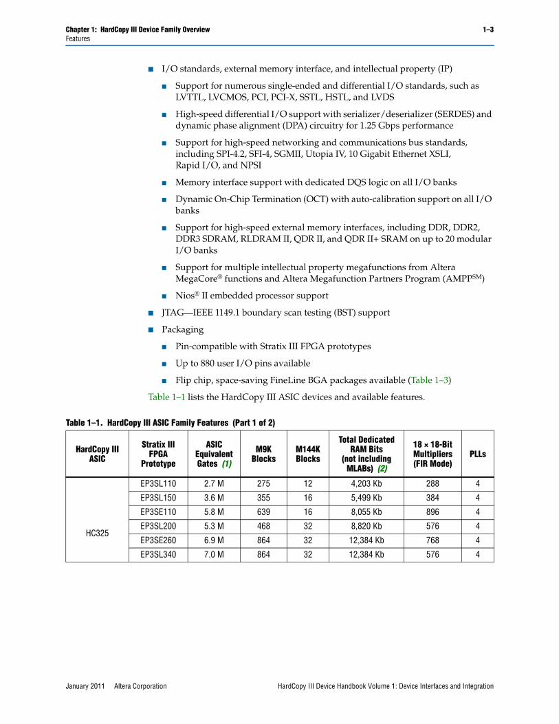
FeaturesHardCopy III devices offer the following features:
■ General
■ Fine-grained HCell architecture resulting in a low-cost, high-performance, low-power ASIC
■ Fully tested production-quality samples typically available 14 weeks from the date of your design submission
■ Design functionality the same as the Stratix III FPGA prototype
■ System performance and power
■ Core logic performance up to 50% faster than the Stratix III FPGA prototype
■ Power consumption reduction of typically 50% or greater from the Stratix III FPGA prototype
■ Robust on-chip hot socketing and power sequencing support
■ Support for instant-on or instant-on-after-50 ms power-up modes
■ I/O:GND:PWR ratio of 8:1:1 along with on-die and on-package decoupling for robust signal integrity
1 The actual performance and power consumption improvements described in this data sheet are design-dependent.
■ Logic and Digital Signal Processing (DSP)
■ 2.7 to 7 million usable gates for both logic and DSP functions (as shown in Table 1–1)
■ High-speed DSP functions supporting 9 × 9, 12 × 12, 18 × 18, and 36 × 36 multipliers, multiple accumulate functions, and finite impulse response (FIR) filters
■ Internal memory
■ TriMatrix memory, consisting of three RAM block sizes to implement true dual-port memory and first-in first-out (FIFO) buffers
■ Up to 16,272 Kbits RAM in embedded RAM blocks (including parity bits)
■ Memory logic array blocks (MLAB) implemented in HCell logic fabric
■ Clock resources PLLs
■ Up to 16 global clocks, 88 regional clocks, and 88 peripheral clocks per device
■ Clock control block supporting dynamic clock network enable/disable and dynamic global clock network source selection
■ Up to 12 PLLs per device supporting PLL reconfiguration, clock switchover, programmable bandwidth, clock synthesis, and dynamic phase shifting
Chapter 1: HardCopy III Device Family Overview 1–3Features
January 2011 Altera Corporation HardCopy III Device Handbook Volume 1: Device Interfaces and Integration
■ I/O standards, external memory interface, and intellectual property (IP)
■ Support for numerous single-ended and differential I/O standards, such as LVTTL, LVCMOS, PCI, PCI-X, SSTL, HSTL, and LVDS
■ High-speed differential I/O support with serializer/deserializer (SERDES) and dynamic phase alignment (DPA) circuitry for 1.25 Gbps performance
■ Support for high-speed networking and communications bus standards, including SPI-4.2, SFI-4, SGMII, Utopia IV, 10 Gigabit Ethernet XSLI, Rapid I/O, and NPSI
■ Memory interface support with dedicated DQS logic on all I/O banks
■ Dynamic On-Chip Termination (OCT) with auto-calibration support on all I/O banks
■ Support for high-speed external memory interfaces, including DDR, DDR2, DDR3 SDRAM, RLDRAM II, QDR II, and QDR II+ SRAM on up to 20 modular I/O banks
■ Support for multiple intellectual property megafunctions from Altera MegaCore® functions and Altera Megafunction Partners Program (AMPPSM)
■ Nios® II embedded processor support
■ JTAG—IEEE 1149.1 boundary scan testing (BST) support
■ Packaging
■ Pin-compatible with Stratix III FPGA prototypes
■ Up to 880 user I/O pins available
■ Flip chip, space-saving FineLine BGA packages available (Table 1–3)
Table 1–1 lists the HardCopy III ASIC devices and available features.
Table 1–1. HardCopy III ASIC Family Features (Part 1 of 2)
HardCopy III ASIC
Stratix III FPGA
Prototype
ASIC Equivalent Gates (1)
M9KBlocks
M144K Blocks
Total Dedicated RAM Bits
(not including MLABs) (2)
18 × 18-Bit Multipliers (FIR Mode)
PLLs
HC325
EP3SL110 2.7 M 275 12 4,203 Kb 288 4
EP3SL150 3.6 M 355 16 5,499 Kb 384 4
EP3SE110 5.8 M 639 16 8,055 Kb 896 4
EP3SL200 5.3 M 468 32 8,820 Kb 576 4
EP3SE260 6.9 M 864 32 12,384 Kb 768 4
EP3SL340 7.0 M 864 32 12,384 Kb 576 4
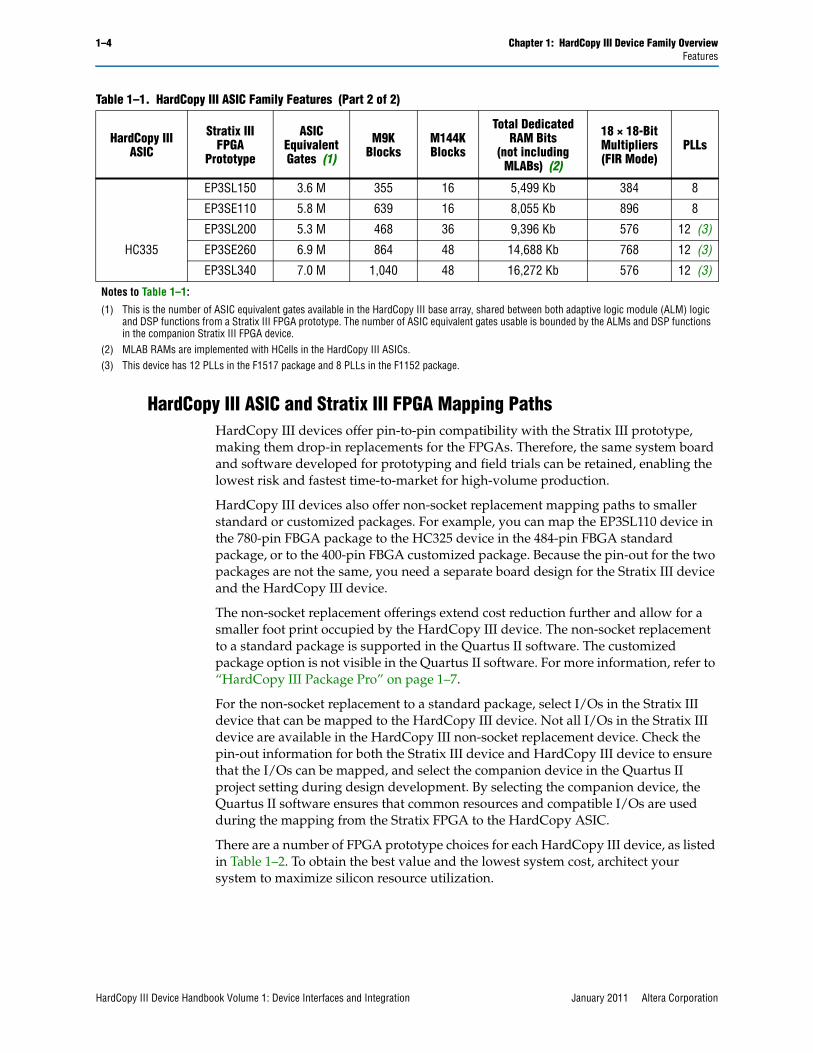
1–4 Chapter 1: HardCopy III Device Family OverviewFeatures
HardCopy III Device Handbook Volume 1: Device Interfaces and Integration January 2011 Altera Corporation
HardCopy III ASIC and Stratix III FPGA Mapping PathsHardCopy III devices offer pin-to-pin compatibility with the Stratix III prototype, making them drop-in replacements for the FPGAs. Therefore, the same system board and software developed for prototyping and field trials can be retained, enabling the lowest risk and fastest time-to-market for high-volume production.
HardCopy III devices also offer non-socket replacement mapping paths to smaller standard or customized packages. For example, you can map the EP3SL110 device in the 780-pin FBGA package to the HC325 device in the 484-pin FBGA standard package, or to the 400-pin FBGA customized package. Because the pin-out for the two packages are not the same, you need a separate board design for the Stratix III device and the HardCopy III device.
The non-socket replacement offerings extend cost reduction further and allow for a smaller foot print occupied by the HardCopy III device. The non-socket replacement to a standard package is supported in the Quartus II software. The customized package option is not visible in the Quartus II software. For more information, refer to “HardCopy III Package Pro” on page 1–7.
For the non-socket replacement to a standard package, select I/Os in the Stratix III device that can be mapped to the HardCopy III device. Not all I/Os in the Stratix III device are available in the HardCopy III non-socket replacement device. Check the pin-out information for both the Stratix III device and HardCopy III device to ensure that the I/Os can be mapped, and select the companion device in the Quartus II project setting during design development. By selecting the companion device, the Quartus II software ensures that common resources and compatible I/Os are used during the mapping from the Stratix FPGA to the HardCopy ASIC.
There are a number of FPGA prototype choices for each HardCopy III device, as listed in Table 1–2. To obtain the best value and the lowest system cost, architect your system to maximize silicon resource utilization.
HC335
EP3SL150 3.6 M 355 16 5,499 Kb 384 8
EP3SE110 5.8 M 639 16 8,055 Kb 896 8
EP3SL200 5.3 M 468 36 9,396 Kb 576 12 (3)
EP3SE260 6.9 M 864 48 14,688 Kb 768 12 (3)
EP3SL340 7.0 M 1,040 48 16,272 Kb 576 12 (3)
Notes to Table 1–1:
(1) This is the number of ASIC equivalent gates available in the HardCopy III base array, shared between both adaptive logic module (ALM) logic and DSP functions from a Stratix III FPGA prototype. The number of ASIC equivalent gates usable is bounded by the ALMs and DSP functions in the companion Stratix III FPGA device.
(2) MLAB RAMs are implemented with HCells in the HardCopy III ASICs.(3) This device has 12 PLLs in the F1517 package and 8 PLLs in the F1152 package.
Table 1–1. HardCopy III ASIC Family Features (Part 2 of 2)
HardCopy III ASIC
Stratix III FPGA
Prototype
ASIC Equivalent Gates (1)
M9KBlocks
M144K Blocks
Total Dedicated RAM Bits
(not including MLABs) (2)
18 × 18-Bit Multipliers (FIR Mode)
PLLs

Chapter 1:HardCopy
III Device Family Overview
1–5Features
January 2011 Altera Corporation
HardCopy III Device Handbook Volume 1: Device Interfaces and Integration
Three different FineLine BGA package substrate options are available for the HardCopy III devices:
■ Performance-optimized flip chip package (F)
■ Cost-optimized flip chip package (L, LA)
■ Low-cost wire bond package (W)
All three package types support direct replacement of the Stratix III FPGA prototype. The performance-optimized flip chip package supports equivalent performance and the same number of I/Os as the corresponding FPGA prototype. The cost-optimized flip chip package uses a substrate with fewer layers and no on-package decoupling (OPD) capacitors to offer a low-cost package option. The performance is reduced from that of the FPGA prototype. However, the number of available I/Os remains the same. The wire bond package offers another low-cost package option, but with the trade-off of reduced performance and fewer available I/Os.
1 If you are going to use the low-cost wire bond package, make sure your design uses I/Os that are available in that package.
For HardCopy III non-socket replacement devices, only the performance-optimized flip chip package and the low-cost wire bond package are supported.
Table 1–2. Stratix III FPGA Prototype to HardCopy III ASIC Mapping Paths (Note 1)
HardCopy III ASIC
HardCopy III Package
Stratix III FPGA Prototype and Package
EP3SL110 EP3SL150 EP3SE110 EP3SL200 EP3SE260 EP3SL340
F780 F780 F1152 F780 F1152 H780 F1152 F1517 H780 F1152 F1517 H1152 F1517
HC325
484-pin FineLine BGA v (2) v (2) — v (2) — v (2) — — v (2) — — v (2) —
780-pin FineLine BGA v v — v — v (3) — — v (3) — — v (2) —
HC335
1152-pin FineLine BGA — — v — v — v — — v — — —
1517-pin FineLine BGA — — — — — — — v — — — v
Notes to Table 1–2:
(1) HardCopy III device migration paths are not supported for the EP3SL50, EP3SL70, EP3SE50, and EP3SE80 Stratix III devices. (2) This mapping is a non-socket replacement path that requires a different board design for the Stratix III device and the HardCopy III device. (3) The Hybrid FBGA package requires additional unused board space along the edges beyond the footprint, but its footprint is compatible with the regular FBGA package.

1–6Chapter 1:
HardCopyIII Device Fam
ily OverviewFeatures
HardCopy III Device Handbook Volume 1: Device Interfaces and Integration
January 2011 Altera Corporation
HardCopy III devices are available in the packages shown in Table 1–3.
Table 1–3. HardCopy III and Stratix III Package, I/O Pin Count, and LVDS Pair Count Mapping Notes (1), (2), (3), (4)
HardCopy III ASIC
WF484FF484 WF780 FF780
LF1152FF1152
LF1517 FF1517
HC325 296, 48 392, 48 488, 56 — —
HC335 — — — 774, 88 880, 88
Companion Mapping
Stratix III FPGA Prototype F780 H780 H1152 F780 H780 H1152 F780 H780 H1152 F1152 H1152 F1517
EP3SL110 488, 56 — — 488, 56 — — 488, 56 — — — — —
EP3SL150 488, 56 — — 488, 56 — — 488, 56 — — 744, 88 — —
EP3SE110 488, 56 — — 488, 56 — — 488, 56 — — 744, 88 — —
EP3SL200 — 488, 56 — — 488, 56 — — 488, 56 — 744, 88 — 976, 88
EP3SE260 — 488, 56 — — 488, 56 — — 488, 56 — 744, 88 — 976, 112
EP3SL340 — 744, 88 — 744, 88 — — 744, 88 — 744, 88 976, 112
Notes to Table 1–3:
(1) The numbers in the table indicate I/O pin count and full duplex LVDS pairs.(2) The first letter in the HardCopy III package name refers to the following: F–Performance-optimized flip-chip package, L–Cost optimized
flip-chip package, W–Low-cost wire bond package.(3) For the F484, F780, and F1152 packaged devices, the I/O pin counts include the eight dedicated clock inputs (CLK1p, CLK1n, CLK3p, CLK3n, CLK8p, CLK8n, CLK10p, and CLK10n) that
can be used for data inputs.(4) For the F1517 packaged devices, the I/O pin counts include the eight dedicated clock inputs (CLK1p, CLK1n, CLK3p, CLK3n, CLK8p, CLK8n, CLK10p, and CLK10n) and the eight dedicated
corner PLL clock inputs (PLL_L1_CLKp, PLL_L1_CLKn, PLL_L4_CLKp, PLL_L4_CLKn, PLL_R4_CLKp, PLL_R4_CLKn, PLL_R1_CLKp, and PLL_R1_CLKn) that can be used for data inputs.

Chapter 1: HardCopy III Device Family Overview 1–7Features
January 2011 Altera Corporation HardCopy III Device Handbook Volume 1: Device Interfaces and Integration
HardCopy III Package Pro The Hardcopy III Package Pro is a customized package program, which gives you the option to select a package tailored to the number of I/O's used in your design. This customized package will support less I/O's than what is available as a standard package offering. HardCopy III Package Pro will have a smaller foot print than a Stratix III FPGA prototype or a HardCopy III non-socket replacement standard package. The optimized package may further extend the cost savings over traditional HardCopy III device offerings.
Table 1–4 lists the available FineLine Ball-Grid Array (FBGA) packages and the maximum supported I/O for HardCopy III devices.
HardCopy III Package Pro is also offered in Ultra FineLine Ball-Grid Array (UBGA) packages. These packages have a 0.8 mm ball pitch, which increases the I/O count when compared to an FPGA package of the same dimension. Table 1–5 lists the available UBGA packages and the maximum supported I/O for HardCopy III devices.
HardCopy III Package Pro is not visible in the Quartus II software, so you will not be able to select a Package Pro device as a companion device to your Stratix III device. However, you still need the Quartus II software to compile your design into an appropriate HardCopy III device prior to migrating to a Package Pro option.
Table 1–4. HardCopy III FBGA Maximum I/O Pin Count
HardCopy III ASIC FF400 FF484 WF572 (1) FF572 WF672 (1) FF672 FF780 FF1020
Package Dimension (mm)
(2)21 × 21 23 × 23 25 × 25 25 × 25 27 × 27 27 × 27 29 × 29 33 × 33
HC325 216 — 336 336 384 384 — —
HC335 — 264 — 304 — 352 456 640
Notes to Table 1–4:
(1) Low-Cost Wirebond Package (W)(2) Dimensions are approximate. See the Altera Device Package Information Datasheet for specifications that resemble the package offering in this
table.
Table 1–5. HardCopy III UBGA Maximum I/O Pin Count
HardCopy III ASIC FU572 FU672 WU780 (1) FU780
Package Dimension (mm) (2) 21 × 21 23 × 23 25 × 25 25 × 25
HC325 336 384 384 480
HC335 — 352 — 456
Notes to Table 1–5:
(1) Low-Cost Wirebond Package (W)(2) Dimensions are approximate. See the Altera Device Package Information Datasheet for specifications that
resemble the package offering in this table.

1–8 Chapter 1: HardCopy III Device Family OverviewFeatures
HardCopy III Device Handbook Volume 1: Device Interfaces and Integration January 2011 Altera Corporation
1 HardCopy III Package Pro details and specifications are not provided in the HardCopy III handbook, and electrical and thermal performance must be considered when designing with Package Pro. Contact your Altera representative to engage the HardCopy III Package Pro program.
Differences Between HardCopy III and Stratix III DevicesHardCopy III devices have several architectural differences from Stratix III devices. When implementing your design and laying out your board, consider these differences. Use the following information to ensure that your design maps from the Stratix III FPGA to the HardCopy III ASIC:
■ Maximum core voltage of 0.9-V in HardCopy III devices compared with selectable core voltages of 0.9-V or 1.1-V in Stratix III devices
■ Maximum VCCIO power supply of 3.0-V
■ HardCopy III power supply ramp time for fast POR mode is 4 ms, and 12 ms for Stratix III devices
■ You may need to use external clamping diodes on the board to keep the pins operating within specification.
■ 3.3-V LVTTL/LVCMOS I/O standard is not supported in HardCopy III devices.
■ Configuration is not required for HardCopy III devices, so the following Stratix III features are not supported:
■ Programming modes and features such as remote update and Programmer Object File (.pof) encryption
■ Cyclical redundancy check (CRC) for configuration error detection
■ 256-bit (AES) volatile and non-volatile security keys to protect designs
■ JTAG instructions used for configuration
■ FPGA configuration emulation mode is not supported in HardCopy III devices.
■ Boundary scan (BSCAN) chain length is different and varies with device density.
■ HardCopy III devices contain up to a maximum of 20 I/O banks compared with 24 I/O banks in the Stratix III devices.
■ Memory Initialization Files (.mif) for embedded memories used as RAM are not supported. The .mifs for memories used as ROM are supported because the data are mask-programmed into the memory cells.
■ Stratix III logic array block (LAB), MLAB, and DSP functions are implemented with HCells in HardCopy III devices instead of dedicated blocks.
■ Stratix III programmable power technology is not supported in HardCopy III devices. However, the HardCopy III architecture offers performance on par with Stratix III devices with significantly lower power.

Chapter 1: HardCopy III Device Family Overview 1–9Architectural Features
January 2011 Altera Corporation HardCopy III Device Handbook Volume 1: Device Interfaces and Integration
Architectural FeaturesThis section describes the architectural features of HardCopy III ASICs.
Logic Array Block and Adaptive Logic Module Function SupportHardCopy III devices fully support the Stratix III LAB and ALM functions. The basic building blocks of Stratix III LABs are composed of ALMs that you can configure to implement logic, arithmetic, and register functions. Each LAB consists of 10 ALMs, carry chains, shared arithmetic chains, LAB control signals, local interconnect, and register chain connection lines.
In HardCopy III devices, the basic building blocks of the core array are HCells, which are a collection of logic transistors connected together to provide the same functionality as the Stratix III LABs and ALMs. The Quartus II software maps these LAB and ALM functions to HCell macros, which define how the HCells are connected together in the HardCopy III core array. Only HCells required to implement the customer design are used, and unused HCells are powered down. This allows efficient use of the core fabric and offers significant static power savings.
The Stratix III LAB derivative, called MLAB, is also supported in HardCopy III devices. The MLAB adds static random access memory (SRAM) capability to the LAB and can provide a maximum of 640 bits of simple dual-port SRAM. Like the LAB functions, the Quartus II software maps MLAB functions to HCell macros in HardCopy III devices to provide the same Stratix III functionality.
f For more information about LABs and ALMs, refer to the Logic Array Block and Adaptive Logic Module Implementation in HardCopy III Devices chapter.
f For more information about MLAB modes, features, and design considerations, refer to the TriMatrix Embedded Memory Blocks in HardCopy III Devices chapter.
DSP Function SupportHardCopy III devices fully support the DSP block functions of Stratix III devices. Complex systems such as WiMAX, 3GPP WCDMA, CDMA2000, voice over Internet protocol (VoIP), H.264 video compression, and high-definition television (HDTV) require high-performance DSP circuits to handle large amounts of data with high throughput. These system designs typically use DSP to implement finite impulse response (FIR) filters, complex FIR filters, infinite impulse response (IIR) filters, fast Fourier transform (FFT) functions, and discrete cosine transform (DCT) functions.
In HardCopy III devices, these DSP block functions are implemented with HCells. The Quartus II software maps the Stratix III DSP functions to HCell macros in HardCopy III devices, preserving the same functionality. Implementing DSP functions using HCells also allows efficient use of the HardCopy III device core fabric and offers significant static power savings.
HardCopy III devices support all Stratix III DSP configurations (9 × 9, 12 × 12, 18 × 18, and 36 × 36 multipliers) and block features, such as dynamic sign controls, dynamic addition and subtraction, dynamic rounding and saturation, and dynamic input shift registers. All five operational modes of the Stratix III DSP block are supported:
■ Independent multiplier (9 × 9, 12 × 12, 18 × 18, and 36 × 36)

1–10 Chapter 1: HardCopy III Device Family OverviewArchitectural Features
HardCopy III Device Handbook Volume 1: Device Interfaces and Integration January 2011 Altera Corporation
■ Two-multiplier adder
■ Four-multiplier adder
■ Multiply accumulate
■ Shift mode
f For more information about DSP blocks, refer to the DSP Block Implementation in HardCopy III Devices chapter.
TriMatrix Embedded Memory BlocksTriMatrix embedded memory blocks provide three different sizes of embedded SRAM to efficiently address the needs of HardCopy III ASIC designs. TriMatrix memory includes the following types of blocks:
■ 640-bit MLAB blocks optimized to implement filter delay lines, small FIFO buffers, and shift registers. MLAB blocks are implemented in HCell macros.
■ 9-Kbit M9K blocks that can be used for general purpose memory applications.
■ 144-Kbit M144K blocks that are ideal for processor code storage, packet, and video frame buffering.
You can configure each embedded memory block independently to be a single- or dual-port RAM, ROM, or shift register using the Quartus II MegaWizard™ Plug-In Manager. Multiple blocks of the same type can also be stitched together to produce larger memories with minimal timing penalty. TriMatrix memory provides up to 16,272 Kbits of dedicated, embedded SRAM.
f For more information about TriMatrix memory blocks, modes, features, and design considerations, refer to the TriMatrix Embedded Memory Blocks in HardCopy III Devices chapter.
Clock Networks and PLLsHardCopy III devices provide dedicated global clock networks (GCLKs), regional clock networks (RCLKs), and periphery clock networks (PCLKs). These clocks are organized into a hierarchical clock structure that provides up to 192 unique clock domains (16 GCLK + 88 RCLK + 88 PCLK) within the HardCopy III device and allows up to 60 unique GCLK/RCLK/PCLK clock sources (16 GCLK + 22 RCLK + 22 PCLK) per device quadrant.
HardCopy III devices deliver abundant PLL resources, with up to 12 PLLs per device and up to 10 outputs per PLL. You can configure each output independently, creating a unique, customizable clock frequency with no fixed relation to any other input or output clock. Inherent jitter filtration and fine granularity control over multiply, divide ratios, and dynamic phase-shift reconfiguration provide the high-performance precision required in today’s high-speed applications. HardCopy III PLLs are feature-rich, supporting advanced capabilities such as clock switchover, reconfigurable phase shift, PLL reconfiguration, and reconfigurable bandwidth. You can use PLLs for general-purpose clock management, supporting multiplication, phase shifting, and programmable duty cycles. HardCopy III PLLs also support external feedback mode, spread-spectrum input clock tracking, and post-scale counter cascading.

Chapter 1: HardCopy III Device Family Overview 1–11Architectural Features
January 2011 Altera Corporation HardCopy III Device Handbook Volume 1: Device Interfaces and Integration
f For more information about clock networks and PLLs, refer to the Clock Networks and PLLs in HardCopy III Devices chapter.
I/O Banks and I/O StructureHardCopy III devices contain up to 20 modular I/O banks, each containing 24, 32, 40, or 48 I/Os (not including dedicated clock inputs). The left- and right-side I/O banks contain circuitry to support external memory interfaces and high-speed differential I/O interfaces capable of performance at up to 1.25 Gbps. The top and bottom I/O banks also contain circuitry to support external memory interfaces.
HardCopy III devices support a wide range of industry I/O standards, including single-ended, voltage referenced single-ended, and differential I/O standards. The HardCopy III I/O supports bus hold, pull-up resistor, slew rate, output delay control, and open-drain output. HardCopy III devices also support on-chip series (RS) and on-chip parallel (RT) termination with auto calibration for single-ended I/O standards. The left and right I/O banks support on-chip differential termination (RD) to meet LVDS I/O standards. Bidirectional I/O pins on all I/O banks also support Dynamic OCT.
f For more information about I/O features, refer to the HardCopy III Device I/O Features chapter.
External Memory InterfacesThe HardCopy III I/O structure is equivalent to the Stratix III I/O structure, providing high-performance support for existing and emerging external memory standards such as DDR, DDR2, DDR3, QDRII, QDRII+, and RLDRAM II.
Packed with features such as dynamic on-chip termination, trace mismatch compensation, read and write leveling, half-rate registers, and 4- to 36-bit DQ group widths, HardCopy III I/Os supply the built-in functionality required for rapid and robust implementation of external memory interfaces. Double data-rate support is found on all sides of the HardCopy III device. HardCopy III devices provide an efficient architecture to quickly and easily fit wide external memory interfaces precisely.
A self-calibrating soft IP core (ALTMEMPHY) optimized to take advantage of HardCopy III device I/Os along with the Quartus II timing analysis tool (the TimeQuest Timing Analyzer) provides the total solution for the highest reliable frequency of operation across process, voltage, and temperature (PVT).
f For more information about external memory interfaces, refer to the External Memory Interfaces in HardCopy III Devices chapter.
High-Speed Differential I/O Interfaces with DPAHardCopy III devices contain dedicated circuitry for supporting differential standards at speeds up to 1.25 Gbps. High-speed differential I/O circuitry supports the following high-speed I/O interconnect standards and applications:
■ Utopia IV
■ SPI-4.2
1–12 Chapter 1: HardCopy III Device Family OverviewArchitectural Features
HardCopy III Device Handbook Volume 1: Device Interfaces and Integration January 2011 Altera Corporation
■ SFI-4
■ 10 Gigabit Ethernet XSLI
■ Rapid I/O
■ NPSI
HardCopy III devices support 2×, 4×, 6×, 7×, 8×, and 10× SERDES modes for high-speed differential I/O interfaces, and 4×, 6×, 7×, 8×, and 10× SERDES modes when using the dedicated DPA circuitry. DPA minimizes bit errors, simplifies PCB layout and timing management for high-speed data transfer, and eliminates channel-to-channel and channel-to-clock skews in high-speed data transmission systems. The Stratix III soft CDR function can also be implemented using HCells in HardCopy III devices, enabling low-cost 1.25-Gbps clock-embedded serial links.
HardCopy III devices have the following dedicated circuitry for high-speed differential I/O support:
■ Differential I/O buffer
■ Transmitter serializer
■ Receiver deserializer
■ Data realignment
■ Dynamic phase aligner (DPA)
■ Soft CDR functionality
■ Synchronizer (FIFO buffer)
■ PLLs
f For more information about dedicated circuitry for high-speed differential support, refer to the High Speed Differential I/O Interfaces with DPA in HardCopy III Devices chapter.
Hot Socketing and Power-On ResetHardCopy III devices offer hot socketing, which is also known as hot plug-in or hot swap, and power sequencing support without the use of any external devices. On-chip hot socketing and power-sequencing support ensures proper device operation independent of the power-up sequence. You can insert or remove a HardCopy III board during system operation without causing undesirable effects to the running system bus or the board itself.
The hot socketing feature also makes it easier to use HardCopy III devices on PCBs that contain a mixture of 3.0-V, 2.5-V, 1.8-V, 1.5-V, and 1.2-V devices. With the HardCopy III hot socketing feature, you do not need to ensure a proper power-up sequence for each device on the board.
1 HardCopy III devices have a maximum VCCIO voltage of 3.0 V, but can tolerate a 3.3-V input level.
f For more information about hot socketing, refer to the Hot Socketing and Power-On Reset in HardCopy III Devices chapter.
Chapter 1: HardCopy III Device Family Overview 1–13Software Support and Part Number Information
January 2011 Altera Corporation HardCopy III Device Handbook Volume 1: Device Interfaces and Integration
IEEE 1149.1 (JTAG) Boundary Scan TestingHardCopy III devices support the JTAG IEEE Std. 1149.1 specification. The Boundary-Scan Test (BST) architecture offers the capability to both test pin connections without using physical test probes and capture functional data while a device is operating normally. Boundary-scan cells in the HardCopy III device can force signals onto pins or capture data from the pin or core signals. Forced test data is serially shifted into the boundary-scan cells. Captured data is serially shifted out and externally compared to expected results.
f For more information about JTAG, refer to the IEEE 1149.1 (JTAG) Boundary Scan Testing in HardCopy III Devices chapter.
Signal IntegrityHardCopy III devices simplify the challenge of maintaining signal integrity through a number of chip-, package-, and board-level enhancements to enable efficient high-speed data transfer into and out of the device. These enhancements include:
■ 8:1:1 user I/O/GND/VCC ratio to reduce loop inductance in the package
■ Dedicated power supply for each I/O bank, with an I/O limit of 24 to 48 I/Os per bank to help limit simultaneous switching noise (SSN)
■ Slew-rate support with up to four settings to match the desired I/O standard, control noise, and overshoot
■ Output-current drive strength support with up to four settings to match desired I/O standard performance
■ Output-delay support to control rise and fall times and adjust duty cycle, compensate for skew, and reduce simultaneous switching output (SSO) noise
■ Dynamic OCT with auto-calibration support for series and parallel OCT and differential OCT support for LVDS I/O standard on the left and right banks
1 The supported settings for slew-rate control, output-current drive strength, and output-delay control are mask-programmed into the HardCopy III devices and cannot be changed after the silicon is fabricated.
f For more information about signal integrity support in the Quartus II software, refer to the Quartus II Handbook.
Software Support and Part Number InformationThis section describes HardCopy III device software support and part number information.

1–14 Chapter 1: HardCopy III Device Family OverviewSoftware Support and Part Number Information
HardCopy III Device Handbook Volume 1: Device Interfaces and Integration January 2011 Altera Corporation
Software SupportHardCopy III devices are supported by the Altera Quartus II design software, which provides a comprehensive environment for system-on-chip (SOC) design. The Quartus II software includes HDL and schematic design entry, compilation and logic synthesis, full simulation and advanced timing analysis, SignalTap™ II logic analyzer, and device configuration.
f For more information about the Quartus II software features, refer to the Quartus II Handbook.
The Quartus II software supports the Windows and Linux Red Hat operating systems. You can obtain the specific operating system for the Quartus II software from the Quartus II Readme.txt file or http://www.altera.com/download/os-support/oss-index.html. The Quartus II software also supports seamless integration with industry-leading EDA tools through the NativeLink interface.
Part Number InformationFigure 1–1 shows the generic part number for HardCopy III devices.
f For more information about a specific package, refer to the HardCopy III Device Package Information chapter.
Figure 1–1. HardCopy III Device Package Ordering Information
F: Performance-optimized flip chip packageL: Cost-optimized flip chip packageW: Low-cost wire bond package
2535
HC3 35 N
Indicates specific device options
N: RoHS compliant
11521517
780484
Package Substrate Type
F: FineLine BGA (FBGA)
HC3: HardCopy III Family
Number of pins for a particular package:
Family Signature
Device Type
Optional Suffix
Pin Count
Package Type
F F 1517

Chapter 1: HardCopy III Device Family Overview 1–15Document Revision History
January 2011 Altera Corporation HardCopy III Device Handbook Volume 1: Device Interfaces and Integration
Document Revision HistoryTable 1–6 lists the revision history for this chapter.
Table 1–6. Document Revision History
Date Version Changes
January 2011 3.2
■ Updated Table 1–1, Table 1–2, and Table 1–3.
■ Updated Figure 1–1.
■ Used new document template.
■ Updated “HardCopy III ASIC and Stratix III FPGA Mapping Paths” on page 1–4.
■ Added “HardCopy III Package Pro” on page 1–7.
■ Made minor text edits.
July 2009 3.1 Updated “Features” on page 1–2.
June 2009 3.0■ Updated Table 1–3, Table 1–6, and Table 1–9 to include non-socket replacement
devices.
■ Updated Figure 1–2.
December 2008 2.0 Edits to Table 1–1.
May 2008 1.0 Initial release.

1–16 Chapter 1: HardCopy III Device Family OverviewDocument Revision History
HardCopy III Device Handbook Volume 1: Device Interfaces and Integration January 2011 Altera Corporation

HardCopy III Device Handbook Volume 1: Device Interfaces and IntegrationJanuary 2011
HIII51002-2.1
Subscribe
© 2011 Altera Corporation. All rights reserved. ALTERA, ARRIA, CYCLONE, HARDCOPY, MAX, MEGACORE, NIOS, QUARTUS and STRATIX are Reg. U.S. Pat. & Tm. Off. and/or trademarks of Altera Corporation in the U.S. and other countries. All other trademarks and service marks are the property of their respective holders as described at www.altera.com/common/legal.html. Altera warrants performance of its semiconductor products to current specifications in accordance with Altera’s standard warranty, but reserves the right to make changes to any products and services at any time without notice. Altera assumes no responsibility or liability arising out of the application or use of any information, product, or service described herein except as expressly agreed to in writing by Altera. Altera customers are advised to obtain the latest version of device specifications before relying on any published information and before placing orders for products or services.
2. Logic Array Block and Adaptive LogicModule Implementation in HardCopy III
Devices
This chapter describes how the Stratix® III’s logic array blocks (LABs) and memory logic array blocks (MLABs) are implemented in a HardCopy® III device.
In Stratix III devices, the core fabric consists of an array of LABs and MLABs. LABs and MLABs are composed of adaptive logic modules (ALMs) that are configurable and can implement various logic, arithmetic, and register functions of a customer design. In addition, MLABs can implement memory functions.
By comparison, the core fabric in HardCopy III devices are built using an array of flexible, fine-grain architecture blocks called HCells that can efficiently implement all the functionality of the ALMs, LABs, and MLABs. HardCopy III devices offer improved performance and significant static power savings compared to Stratix III FPGA prototype devices because only the HCells required to implement the customer design are used, while the unused HCells are powered down.
f For more information about ALMs, LABs, and MLABs, refer to the Logic Array Blocks and Adaptive Logic Modules in Stratix III Devices chapter in volume 1 of the Stratix III Device Handbook.
This chapter contains the following sections:
■ “HCells”
■ “ALM and LAB Function Implementation” on page 2–2
■ “MLAB Function Implementation” on page 2–4
HCellsHCells are a collection of logic transistors based on 0.9-V, 40-nm process technology. The construction of logic using HCells allows flexible functionality such that when HCells are combined, all viable logic combinations of Stratix III functionality are replicated. These HCells constitute the array of the HCell area, as shown in Figure 2–1. Only the HCells needed to implement the design are assembled together, which optimizes HCell use. The unused area of the HCell logic fabric is powered down, resulting in significant static power savings compared with the Stratix III FPGA prototype.
January 2011HIII51002-2.1

2–2 Chapter 2: Logic Array Block and Adaptive Logic Module Implementation in HardCopy III DevicesALM and LAB Function Implementation
HardCopy III Device Handbook Volume 1: Device Interfaces and Integration January 2011 Altera Corporation
ALM and LAB Function ImplementationThe Quartus II software uses a library of pre-characterized HCell macros (HCMs) to place Stratix III ALM configurations into the HardCopy III HCell-based logic fabric. An HCell macro defines how a group of HCells connect within the array. HCell macros can construct all combinations of combinational logic, adder, and register functions that can be implemented by a Stratix III ALM. You can use HCells that are not used for ALM configurations to implement MLAB and DSP block functions.
f For more details about implementing DSP block functions using HCells, refer to the DSP Block Implementation in HardCopy III Devices chapter.
Figure 2–1. Example Block Diagram of HardCopy III Device (Note 1)
Notes to Figure 2–1:
(1) Figure 2–1 shows a graphical representation of the device floorplan. A detailed floorplan is available in the Quartus® II software.(2) IOEs represents I/O elements.
IOEs PLL
IOEs (2)
PLL
Array of HCells M144K Blocks M9K Blocks

Chapter 2: Logic Array Block and Adaptive Logic Module Implementation in HardCopy III Devices 2–3ALM and LAB Function Implementation
January 2011 Altera Corporation HardCopy III Device Handbook Volume 1: Device Interfaces and Integration
Based on design requirements, the Quartus II software chooses the appropriate HCell macros to implement design functionality. For example, Stratix III ALMs offer flexible look-up table (LUT) blocks, registers, arithmetic blocks, and LAB-wide control signals. In HardCopy III devices, if your design requires these architectural elements, the Quartus II synthesis tool maps the design to the appropriate HCell macros, resulting in improved design performance compared to the Stratix III FPGA prototype, as shown in Figure 2–2.
Figure 2–2. Example of ALM Functions Mapped to HCell Macros
Logic FunctionHCM
Logic FunctionHCM
Adder HCM
Register HCM
Comb.Logic
Adder
Adder
Reg
Reg
HardCopy III
Stratix III

2–4 Chapter 2: Logic Array Block and Adaptive Logic Module Implementation in HardCopy III DevicesMLAB Function Implementation
HardCopy III Device Handbook Volume 1: Device Interfaces and Integration January 2011 Altera Corporation
MLAB Function ImplementationIn Stratix III devices, the MLAB is a LAB derivative that you can configure to support up to a maximum of 640 bits of simple dual-port static random access memory (SRAM). Similar to the LAB, each MLAB consists of ten ALMs and can implement all the functionality of the LAB in addition to the memory function. In HardCopy III devices, the MLAB functions are mapped to HCell macros that provide the same memory functionality.
f For more information about memory implementation using MLABs, refer to the TriMatrix Embedded Memory Blocks in Stratix III Devices chapter in volume 1 of the Stratix III Device Handbook.
f For more information about HardCopy III memory support, refer to the TriMatrix Embedded Memory Blocks in HardCopy III Devices chapter.
In HardCopy III devices, the basic building block of the core array is the HCell. HCells are connected together to form HCell macros that can implement all the functionality of the ALMs, LABs, and MLABs in the Stratix III devices. Only HCells required to implement the design are used, while unused HCells are powered down. This allows the core fabric to be efficiently used and offers significant static power savings compared to the Stratix III FPGA prototype devices.
Document Revision HistoryTable 2–1 shows the revision history for this chapter.
Table 2–1. Document Revision History
Date Version Changes Made
January 2011 2.1■ Maintenance release—used new document template.
■ Minor text edits.
December 2008 2.0 Added Introductory paragraph.
May 2008 1.0 Initial release.

HardCopy III Device Handbook Volume 1: Device Interfaces and IntegrationJanuary 2011
HIII51003-2.1
Subscribe
© 2011 Altera Corporation. All rights reserved. ALTERA, ARRIA, CYCLONE, HARDCOPY, MAX, MEGACORE, NIOS, QUARTUS and STRATIX are Reg. U.S. Pat. & Tm. Off. and/or trademarks of Altera Corporation in the U.S. and other countries. All other trademarks and service marks are the property of their respective holders as described at www.altera.com/common/legal.html. Altera warrants performance of its semiconductor products to current specifications in accordance with Altera’s standard warranty, but reserves the right to make changes to any products and services at any time without notice. Altera assumes no responsibility or liability arising out of the application or use of any information, product, or service described herein except as expressly agreed to in writing by Altera. Altera customers are advised to obtain the latest version of device specifications before relying on any published information and before placing orders for products or services.
3. DSP Block Implementation inHardCopy III Devices
HardCopy® III devices use HCells to implement the digital signal processing (DSP) block functions of Stratix® III devices, and support all Stratix III DSP operational modes. Implementing DSP functions using HCells allows the HardCopy III device core fabric to be used efficiently and offers significant static power savings compared with Stratix III prototype devices.
Stratix III devices have dedicated high-performance DSP blocks that are distributed throughout the core fabric. These hard-wired DSP blocks are ideal for applications such as high performance computing (HPC), video compression/decompression, and voice over internet protocol (VoIP). Such applications typically require a large number of mathematical computations. Stratix III DSP blocks consist of a combination of dedicated elements that perform multiplication, addition, subtraction, accumulation, summation, and dynamic shift operations.
In HardCopy III devices, these DSP functions are constructed using HCells instead of dedicated DSP blocks. HCells allow HardCopy III devices to have the same functionality as Stratix III DSP blocks. In addition, DSP blocks implemented with HCells provide significant static power savings because only the HCells needed to implement the functions are used.
This chapter contains the following sections:
■ “DSP Function Implementation”
■ “DSP Operational Mode and Feature Support” on page 3–3
DSP Function ImplementationA Stratix III DSP block consists of an input register bank, multiplier adders, pipeline register bank, second-stage adders/accumulator, round and saturation units, and second adder register and output register bank. In HardCopy III devices, HCells make up the device logic fabric. HCells are a collection of logic transistors that are connected together to provide the same DSP functions as the Stratix III DSP blocks. HCells are also used to implement the Stratix III adaptive logic module (ALM) and logic array block (LAB) functions in the HardCopy III devices.
f For more information about ALM, LAB, and memory logic array block (MLAB) implementation in HardCopy III devices, refer to the Logic Array Block and Adaptive Logic Module Implementation in HardCopy III Devices chapter.
The Quartus® II software uses a library of pre-characterized HCell macros (HCMs) to place Stratix III DSP configurations into the HardCopy III HCell-based logic fabric. An HCM defines how a group of HCells are connected together. Based on design requirements, the Quartus II software chooses the appropriate DSP HCell macros to implement the DSP functionality. In HardCopy III devices, HCell macros implement Stratix III DSP block functionality with area efficiency and performance on par with the dedicated DSP blocks in Stratix III devices.
January 2011HIII51003-2.1

3–2 Chapter 3: DSP Block Implementation in HardCopy III DevicesDSP Function Implementation
HardCopy III Device Handbook Volume 1: Device Interfaces and Integration January 2011 Altera Corporation
Only HCells that are required to implement the design’s DSP functions are enabled. HCells not needed for DSP functions can be used for ALM configurations, which results in efficient logic usage. In addition to area management, the placement of these HCell macros allows for optimized routing and performance.
An example of efficient logic area usage is evident when comparing the 18 × 18 independent multiplier implementation in Stratix III devices using the dedicated DSP block versus the implementation in HardCopy III devices using HCells. If the Stratix III DSP function only calls for one 18 × 18 multiplier, the other three 18 × 18 multipliers and the DSP block's adder output block are not used, as shown in Figure 3–1. In HardCopy III devices, the HCell-based logic fabric that is not used for DSP functions can be used to implement other combinational logic, adder, register, and MLAB functions.
Figure 3–1. Stratix III DSP Block versus HardCopy III HCell 18 × 18-Bit Independent Multiplier Implementation
InputRegisters
18 × 18Multiplier
18 × 18Multiplier
18 × 18Multiplier
18 × 18Multiplier
InputRegisters
OutputRegisters
OutputRegisters
Adder/Subtractor/
AccumulatorBlock
InputRegisters
18 × 18Multiplier
OutputRegisters
Used portions of the block
Unused portions of the block
Stratix III DSP Block HardCopy III HCell-Based Logic Fabric
These elements are implementedusing HCell macros.
Unused logic area canbe used to perform other
logic functions.

Chapter 3: DSP Block Implementation in HardCopy III Devices 3–3DSP Operational Mode and Feature Support
January 2011 Altera Corporation HardCopy III Device Handbook Volume 1: Device Interfaces and Integration
DSP Operational Mode and Feature SupportHardCopy III devices support all Stratix III DSP configurations (9 × 9, 12 × 12, 18 × 18, and 36 × 36 multipliers) and all Stratix III DSP block features, such as dynamic sign controls, dynamic addition/subtraction, dynamic rounding and saturation, and dynamic input shift registers.
HardCopy III devices use DSP HCell macros to implement all five operational modes of the Stratix III DSP block:
■ Independent Multiplier (9 × 9, 12 × 12, 18 × 18, 36 × 36)
■ Two-Multiplier Adder
■ Four-Multiplier Adder
■ Multiply Accumulate
■ Shift
f For more information about Stratix III DSP blocks, refer to the DSP Blocks in Stratix III Devices chapter in volume 1 of the Stratix III Device Handbook.
Depending on the Stratix III DSP configurations, the Quartus II software partitions the DSP function into a combination of DSP HCell macros for the HardCopy III devices. This optimizes the DSP function and allows the core fabric to be used more efficiently.
Document Revision HistoryTable 3–1 shows the revision history for this document.
Table 3–1. Document Revision History
Date Version Changes
January 2011 2.1■ Maintenance release—used new document template.
■ Minor text edits.
December 2008 2.0■ Updated “DSP Function Implementation” section.
■ Made minor editorial changes.
May 2008 1.0 Initial release.

3–4 Chapter 3: DSP Block Implementation in HardCopy III DevicesDocument Revision History
HardCopy III Device Handbook Volume 1: Device Interfaces and Integration January 2011 Altera Corporation
HardCopy III Device Handbook Volume 1: Device Interfaces and IntegrationJanuary 2011
HII51004-3.1
Subscribe
© 2011 Altera Corporation. All rights reserved. ALTERA, ARRIA, CYCLONE, HARDCOPY, MAX, MEGACORE, NIOS, QUARTUS and STRATIX are Reg. U.S. Pat. & Tm. Off. and/or trademarks of Altera Corporation in the U.S. and other countries. All other trademarks and service marks are the property of their respective holders as described at www.altera.com/common/legal.html. Altera warrants performance of its semiconductor products to current specifications in accordance with Altera’s standard warranty, but reserves the right to make changes to any products and services at any time without notice. Altera assumes no responsibility or liability arising out of the application or use of any information, product, or service described herein except as expressly agreed to in writing by Altera. Altera customers are advised to obtain the latest version of device specifications before relying on any published information and before placing orders for products or services.
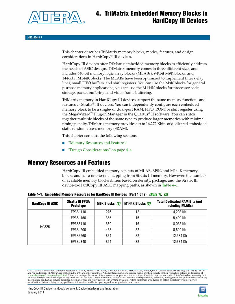
4. TriMatrix Embedded Memory Blocks inHardCopy III Devices
This chapter describes TriMatrix memory blocks, modes, features, and design considerations in HardCopy® III devices.
HardCopy III devices offer TriMatrix embedded memory blocks to efficiently address the needs of ASIC designs. TriMatrix memory comes in three different sizes and includes 640-bit memory logic array blocks (MLABs), 9-Kbit M9K blocks, and 144-Kbit M144K blocks. The MLABs have been optimized to implement filter delay lines, small FIFO buffers, and shift registers. You can use the M9K blocks for general purpose memory applications; you can use the M144K blocks for processor code storage, packet buffering, and video frame buffering.
TriMatrix memory in HardCopy III devices support the same memory functions and features as Stratix® III devices. You can independently configure each embedded memory block to be a single- or dual-port RAM, FIFO, ROM, or shift register using the MegaWizard™ Plug-in Manager in the Quartus® II software. You can stitch together multiple blocks of the same type to produce larger memories with minimal timing penalty. TriMatrix memory provides up to 16,272 Kbits of dedicated embedded static random access memory (SRAM).
This chapter contains the following sections:
■ “Memory Resources and Features”
■ “Design Considerations” on page 4–4
Memory Resources and FeaturesHardCopy III embedded memory consists of MLAB, M9K, and M144K memory blocks and has a one-to-one mapping from Stratix III memory. However, the number of available memory blocks differs based on density, package, and the Stratix III device-to-HardCopy III ASIC mapping paths, as shown in Table 4–1.
Table 4–1. Embedded Memory Resources for HardCopy III Devices (Part 1 of 2) (Note 1), (2)
HardCopy III ASIC Stratix III FPGA Prototype M9K Blocks (3) M144K Blocks (3) Total Dedicated RAM Bits (not
including MLABs)
HC325
EP3SL110 275 12 4,203 Kb
EP3SL150 355 16 5,499 Kb
EP3SE110 639 16 8,055 Kb
EP3SL200 468 32 8,820 Kb
EP3SE260 864 32 12,384 Kb
EP3SL340 864 32 12,384 Kb
January 2011HII51004-3.1

4–2 Chapter 4: TriMatrix Embedded Memory Blocks in HardCopy III DevicesMemory Resources and Features
HardCopy III Device Handbook Volume 1: Device Interfaces and Integration January 2011 Altera Corporation
With regards to functionality, memory in HardCopy III devices and Stratix III devices is identical. The memory blocks can implement various types of memory with or without parity, including true dual-port, simple dual-port, and single-port RAM, ROM, and FIFO. Table 4–2 lists the size and features of the different memory blocks. In addition, unused memory blocks in HardCopy III devices are powered down, allowing the HardCopy III devices to have significant power savings.
HC335
EP3SL150 355 16 5,499 Kb
EP3SE110 639 16 8,055 Kb
EP3SL200 468 36 9,396 Kb
EP3SE260 864 48 14,688 Kb
EP3SL340 1,040 48 16,272 Kb
Notes to Table 4–1:
(1) In addition to device resource usage, Stratix III packages also determine the optimal HardCopy III device mapping path. For example, the EP3SL150 device comes in F780 and F1152 packages. The mapping paths for the F780 and F1152 packages are the HC325 and HC335 devices, respectively.
(2) HardCopy III devices do not have dedicated MLAB blocks but can support the same Stratix III MLAB functionality. The number of MLABs that are supported in HardCopy III devices varies depending on resource usage and the Stratix III device to HardCopy III device mapping path.
(3) The M9K and M144K blocks may lock up if there is a glitch in the clock source when rden equals 1. For more information and the workaround solution, refer to M9K and M144K RAM Block Lockup Issue in the Stratix III Device Family Errata Sheet.
Table 4–1. Embedded Memory Resources for HardCopy III Devices (Part 2 of 2) (Note 1), (2)
HardCopy III ASIC Stratix III FPGA Prototype M9K Blocks (3) M144K Blocks (3) Total Dedicated RAM Bits (not
including MLABs)
Table 4–2. Embedded Memory Features for HardCopy III Devices (Part 1 of 2) (1)
Feature MLABs M9K Blocks M144K Blocks
Maximum performance TBD TBD TBD
Total RAM bits (including parity bits) 640 9,216 147,456
Configurations (depth × width)
16 × 8
16 × 9
16 × 10
16 × 16
16 × 18
16 × 20
(1)
8K × 1
4K × 2
2K × 4
1K × 8
1K × 9
512 × 16
512 × 18
256 × 32
256 × 36
16K × 8
16K × 9
8K × 16
8K × 18
4K × 32
4K × 36
2K × 64
2K × 72
Parity bits v v vByte enable v v vPacked mode — v vAddress clock enable v v vSingle-port memory v v vSimple dual-port memory v v vTrue dual-port memory — v vEmbedded shift register v v vROM (2) v v v
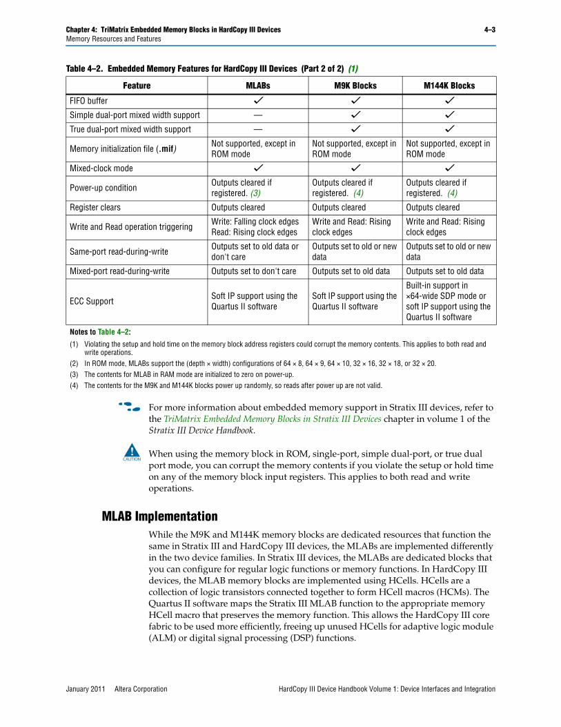
Chapter 4: TriMatrix Embedded Memory Blocks in HardCopy III Devices 4–3Memory Resources and Features
January 2011 Altera Corporation HardCopy III Device Handbook Volume 1: Device Interfaces and Integration
f For more information about embedded memory support in Stratix III devices, refer to the TriMatrix Embedded Memory Blocks in Stratix III Devices chapter in volume 1 of the Stratix III Device Handbook.
c When using the memory block in ROM, single-port, simple dual-port, or true dual port mode, you can corrupt the memory contents if you violate the setup or hold time on any of the memory block input registers. This applies to both read and write operations.
MLAB ImplementationWhile the M9K and M144K memory blocks are dedicated resources that function the same in Stratix III and HardCopy III devices, the MLABs are implemented differently in the two device families. In Stratix III devices, the MLABs are dedicated blocks that you can configure for regular logic functions or memory functions. In HardCopy III devices, the MLAB memory blocks are implemented using HCells. HCells are a collection of logic transistors connected together to form HCell macros (HCMs). The Quartus II software maps the Stratix III MLAB function to the appropriate memory HCell macro that preserves the memory function. This allows the HardCopy III core fabric to be used more efficiently, freeing up unused HCells for adaptive logic module (ALM) or digital signal processing (DSP) functions.
FIFO buffer v v vSimple dual-port mixed width support — v vTrue dual-port mixed width support — v vMemory initialization file (.mif) Not supported, except in
ROM modeNot supported, except in ROM mode
Not supported, except in ROM mode
Mixed-clock mode v v vPower-up condition Outputs cleared if
registered. (3) Outputs cleared if registered. (4)
Outputs cleared if registered. (4)
Register clears Outputs cleared Outputs cleared Outputs cleared
Write and Read operation triggering Write: Falling clock edges Read: Rising clock edges
Write and Read: Rising clock edges
Write and Read: Rising clock edges
Same-port read-during-write Outputs set to old data or don't care
Outputs set to old or new data
Outputs set to old or new data
Mixed-port read-during-write Outputs set to don't care Outputs set to old data Outputs set to old data
ECC Support Soft IP support using the Quartus II software
Soft IP support using the Quartus II software
Built-in support in ×64-wide SDP mode or soft IP support using the Quartus II software
Notes to Table 4–2:
(1) Violating the setup and hold time on the memory block address registers could corrupt the memory contents. This applies to both read and write operations.
(2) In ROM mode, MLABs support the (depth × width) configurations of 64 × 8, 64 × 9, 64 × 10, 32 × 16, 32 × 18, or 32 × 20.(3) The contents for MLAB in RAM mode are initialized to zero on power-up.(4) The contents for the M9K and M144K blocks power up randomly, so reads after power up are not valid.
Table 4–2. Embedded Memory Features for HardCopy III Devices (Part 2 of 2) (1)
Feature MLABs M9K Blocks M144K Blocks

4–4 Chapter 4: TriMatrix Embedded Memory Blocks in HardCopy III DevicesDesign Considerations
HardCopy III Device Handbook Volume 1: Device Interfaces and Integration January 2011 Altera Corporation
f For more information about HCells in HardCopy III devices, refer to the Logic Array Block and Adaptive Logic Module Implementation in HardCopy III Devices chapter.
Design ConsiderationsUnlike Stratix III devices, HardCopy III devices do not have device configuration, so memories that are configured as RAM power up with random content. Therefore, the memory block contents cannot be pre-loaded or initialized with a memory initialization file (.mif) in HardCopy III devices. You must ensure that your Stratix III design does not require .mifs if you use the memory blocks as RAM. However, if you use the memory blocks as ROM, they are mask programmed to the design’s ROM contents.
1 You can use the ALTMEM_INIT megafunction to initialize the RAM after power up for HardCopy III devices. This megafunction reads from an internal ROM (inside the megafunction) or an external ROM (on chip or off chip) and writes to the RAM after power up.
When using non-registered output mode for the HardCopy III MLAB memory blocks, the outputs power up with memory content. When using registered output mode for these memory blocks, the outputs are cleared on power up. You must take this into consideration when designing logic that might evaluate the initial power up values of the MLAB memory block.
Document Revision HistoryTable 4–3 lists the revision history for this chapter.
Table 4–3. Document Revision History
Date Version Changes
January 2011 3.1
■ Update Table 4–1 and Table 4–2.
■ Updated the “Memory Resources and Features” section.
■ Minor text edits.
June 2009 3.0
■ Updated Table 4–1.
■ Minor text edits.
■ Removed the Conclusion and Referenced Documents sections.
December 2008 2.0■ Updated Table 4–1.
■ Made minor editorial changes.
May 2008 1.0 Initial release.
HardCopy III Device Handbook Volume 1: Device Interfaces and IntegrationJanuary 2011
HIII51005-3.1
Subscribe
© 2011 Altera Corporation. All rights reserved. ALTERA, ARRIA, CYCLONE, HARDCOPY, MAX, MEGACORE, NIOS, QUARTUS and STRATIX are Reg. U.S. Pat. & Tm. Off. and/or trademarks of Altera Corporation in the U.S. and other countries. All other trademarks and service marks are the property of their respective holders as described at www.altera.com/common/legal.html. Altera warrants performance of its semiconductor products to current specifications in accordance with Altera’s standard warranty, but reserves the right to make changes to any products and services at any time without notice. Altera assumes no responsibility or liability arising out of the application or use of any information, product, or service described herein except as expressly agreed to in writing by Altera. Altera customers are advised to obtain the latest version of device specifications before relying on any published information and before placing orders for products or services.
5. Clock Networks and PLLs inHardCopy III Devices
This chapter provides a general description of clock networks and phase-locked loops (PLLs) in HardCopy® III devices.
HardCopy III devices support a hierarchical clock structure and multiple PLLs with advanced features equivalent to Stratix® III devices. The large number of clocking resources in combination with clock synthesis precision offered by the PLLs provides a complete clock management solution for your designs. HardCopy III devices provide dedicated global clock networks (GCLKs), regional clock networks (RCLKs), and periphery clock networks (PCLKs). These clocks are organized into a hierarchical clock structure that provides up to 192 unique clock domains for the entire device, and up to 60 unique clock sources per device quadrant. Altera’s Quartus® II software compiler automatically turns off clock networks not used in the design, thereby reducing overall power consumption of the device.
HardCopy III devices deliver abundant PLL resources with up to 12 PLLs per device and up to 10 outputs per PLL. These PLLs are feature rich, supporting advanced capabilities such as clock switchover, dynamic phase shifting, PLL reconfiguration, and reconfigurable bandwidth. HardCopy III PLLs also support external feedback mode, spread-spectrum tracking, and post-scale counter cascading features. The Quartus II software enables the PLLs and their features without requiring any external devices.
1 All Stratix III PLL features are supported by HardCopy III PLLs.
f For detailed information about clock networks and PLLs, refer to the Clock Networks and PLLs in Stratix III Devices chapter in volume 1 of the Stratix III Device Handbook.
Clock Networks in HardCopy III DevicesHardCopy III devices offer the same clock network resources and features as Stratix III devices. Clock resources that are used in Stratix III devices are mapped to equivalent clock resources in HardCopy III devices, preserving the clocking functions. Unused clock resources are powered down to reduce power consumption.
Clock Network ResourcesSimilar to Stratix III devices, HardCopy III devices have up to 32 dedicated single-ended clock pins or 16 dedicated differential clock pins (CLK[0:15]p and CLK[0:15]n) that can drive either the GCLK or RCLK networks. These clock pins are arranged in the middle of the four sides of the HardCopy III device.
You can drive the 16 GCLKs in HardCopy III devices throughout the entire device, serving as low-skew clock sources for the core fabric and PLLs. You can also drive the GCLKs from the device I/O elements (IOEs) and internal logic to generate global clocks and other high fan-out control signals.
January 2011HIII51005-3.1

Chapter 5: Clock Networks and PLLs in HardCopy III Devices 5–2Clock Networks in HardCopy III Devices
January 2011 Altera Corporation HardCopy III Device Handbook Volume 1: Device Interfaces and Integration
The RCLKs provide the lowest clock delay and skew for logic contained within a single device quadrant. You can drive RCLKs from IOEs and internal logic within a given quadrant.
The PCLKs are a collection of individual clock networks driven from the periphery of the HardCopy III device. Clock outputs from the dynamic phase alignment (DPA) block, horizontal I/O pins, and internal logic can drive the PCLK networks. These PCLKs have higher skew when compared with the GCLK and RCLK networks and can be used instead of general purpose routing to drive signals into and out of the HardCopy III device.
The GCLKs, RCLKs, and PCLKs available in HardCopy III devices are organized into hierarchical clock structures that provide up to 192 unique clock domains (16 GCLK + 88 RCLK + 88 PCLK) across the entire device. HardCopy III devices also allow up to 60 unique GCLK, RCLK, and PCLK clock sources (16 GCLK + 22 RCLK + 22 PCLK) per device quadrant.
Table 5–1 lists the clock resources available in HardCopy III devices.
Table 5–1. Clock Resources in HardCopy III Devices
Clock ResourceNumber of Resources Available
Source of Clock Resource
Clock input pins 32 Single-ended(16 Differential) CLK[0..15]p and CLK[0..15]n pins
Global clock networks 16 CLK[0..15]p/n pins, PLL clock outputs, and logic array
Regional clock networks 88 CLK[0..15]p/n pins, PLL clock outputs, and logic array
Peripheral clock networks 88 (22 per device quadrant) (1) DPA clock outputs, horizontal I/O pins, and logic array
GCLKs/RCLKs per quadrant 38 16 GCLKs + 22 RCLKs
GCLKs/RCLKs per device 104 16 GCLKs + 88 RCLKs
Note to Table 5–1:
(1) There are 56 PCLKs in HC325 devices and 88 PCLKs in HC335 devices.

Chapter 5: Clock Networks and PLLs in HardCopy III Devices 5–3PLLs in HardCopy III Devices
January 2011 Altera Corporation HardCopy III Device Handbook Volume 1: Device Interfaces and Integration
Clocking RegionsHardCopy III devices can implement the four different types of Stratix III clocking regions using GCLK and RCLK networks. These types of clocking regions include the following:
■ Entire device clock region
■ Regional clock region
■ Dual-regional clock region
■ Sub-regional clock region
Clock Control BlockHardCopy III devices also support the same features as the Stratix III clock control block, which is available for each GCKL and RCLK network. The clock control block provides the following features:
■ Clock source selection (dynamic selection for GCLKs)
You can statically or dynamically select the GCLK source. The RCLK source can only be statically selected. Static selection involves mask programming the clock multiplexer select inputs. The clock selection is fixed and cannot be changed when the HardCopy III device is in user mode. Dynamic selection for the GCLK source uses internal logic to control the clock multiplexer select inputs when the device is in user mode. For dynamic clock source selection, you can either select two PLL outputs (such as CLK0 or CLK1) or a combination of clock pins or PLL outputs.
■ Clock power-down (static or dynamic clock enable or disable)
You can statically or dynamically power-down the GCLK and RCLK networks, reducing overall power consumption of the device. Unused GCLK and RCLK networks are powered down through static settings that are automatically generated by the Quartus II software and mask programmed into the device. The dynamic clock enable or disable feature allows internal logic to synchronously control power-up or power-down on GCLK and RCLK networks, including dual-regional clock regions.
PLLs in HardCopy III DevicesHardCopy III devices offer up to 12 PLLs that support the same features as the Stratix III PLLs. These PLLs provide robust clock management and synthesis for device clock management, external system clock management, and high-speed I/O interfaces. The nomenclature for the PLLs follows their geographical location in the device floorplan. The PLLs that reside on the top and bottom sides of the device are named PLL_T1, PLL_T2, PLL_B1, and PLL_B2
The PLLs that reside on the left and right sides of the device are named PLL_L1, PLL_L2, PLL_L3, PLL_L4, PLL_R1, PLL_R2, PLL_R3, and PLL_R4, respectively.

Chapter 5: Clock Networks and PLLs in HardCopy III Devices 5–4PLLs in HardCopy III Devices
January 2011 Altera Corporation HardCopy III Device Handbook Volume 1: Device Interfaces and Integration
Table 5–2 lists the number of PLLs available in the HardCopy III device family.
Table 5–2. HardCopy III Device PLL Availability (Part 1 of 2)
HardCopy III Device
Stratix III Prototype Device L1 L2 L3 L4 T1 T2 B1 B2 R1 R2 R3 R4
HC325WF484
EP3SL110--F780 (1) — — — — — — — —
EP3SL150--F780 (1) — — — — — — — —
EP3SE110--F780 (1) — — — — — — — —
EP3SL200--H780 (1) — — — — — — — —
EP3SE260--H780 (1) — — — — — — — —
EP3SL340--H1152 (1) (2) — () — () () — () —
HC325FF484
EP3SL110--F780 (1) — — — — — — —
EP3SL150--F780 (1) — — — — — — —
EP3SE110--F780 (1) — — — — — — —
EP3SL200--H780 (1) — — — — — — —
EP3SE260--H780 (1) — — — — — — —
EP3SL340--H1152 (1) (2) — () — () () — () —
HC325WF780
EP3SL110--F780 — — — — — — —
EP3SL150--F780 — — — — — — —
EP3SE110--F780 — — — — — — —
EP3SL200--H780 — — — — — — —
EP3SE260--H780 — — — — — — —
EP3SL340--H1152 (1) (2) — () — () () — () —
HC325FF780
EP3SL110--F780 — — — — — — —
EP3SL150--F780 — — — — — — —
EP3SE110--F780 — — — — — — —
EP3SL200--H780 — — — — — — —
EP3SE260--H780 — — — — — — —
EP3SL340--H1152 (1) (2) — () — () () — () —
HC335LF1152
EP3SL150--F1152 — — — —
EP3SE110--F1152 — — — —
EP3SL200--F1152 — — — —
EP3SE260--F1152 — — — —
EP3SL340--H1152 — — — —

Chapter 5: Clock Networks and PLLs in HardCopy III Devices 5–5PLLs in HardCopy III Devices
January 2011 Altera Corporation HardCopy III Device Handbook Volume 1: Device Interfaces and Integration
The PLL functionality in HardCopy III devices remains the same as in Stratix III PLLs. Therefore, HardCopy III PLLs also support features such as PLL reconfiguration, where you can dynamically configure the PLL in user mode.
All HardCopy III PLLs have the same core analog structure with only minor differences in features that are supported. Table 5–3 lists the features of the top/bottom and left/right PLLs in HardCopy III devices.
f For more information about Stratix III PLL features, refer to the Clock Networks and PLLs in Stratix III Devices chapter in volume 1 of the Stratix III Device Handbook.
HC335FF1152
EP3SL150--F1152 — — — —
EP3SE110--F1152 — — — —
EP3SL200--F1152 — — — —
EP3SE260--F1152 — — — —
EP3SL340--H1152 — — — —
HC335LF1517
EP3SL200--F1517
EP3SE260--F1517
EP3SL340--F1517
HC335FF1517
EP3SL200--F1517
EP3SE260--F1517
EP3SL340--F1517
NOTE: to Table 5–2
(1) These are non-socket replacement devices. A board redesign is required.(2) The HardCopy device has four PLLs, whereas the FPGA prototype device has eight PLLs. The additional PLLs available only in the FPGA
prototype device are marked ().
Table 5–2. HardCopy III Device PLL Availability (Part 2 of 2)
HardCopy III Device
Stratix III Prototype Device L1 L2 L3 L4 T1 T2 B1 B2 R1 R2 R3 R4
Table 5–3. HardCopy III PLL Features (Part 1 of 2)
Feature HardCopy III Top/Bottom PLLs HardCopy III Left/Right PLLs
C (output) counters 10 7
M, N, C counter sizes 1 to 512 1 to 512
Dedicated clock outputs 6 single-ended or 4 single-ended and 1 differential pair 2 single-ended or 1 differential pair
Clock input pins 8 single-ended or 4 differential pin pairs 8 single-ended or 4 differential pin pairs
External feedback input pin Single-ended or differential Single-ended only
Spread-spectrum input clock tracking Yes (1) Yes (1)
PLL cascading Through GCLK and RCLK, and dedicated path between adjacent PLLs
Through GCLK and RCLK, and dedicated path between adjacent PLLs (2)
Compensation modes All except LVDS clock network compensation
All except external feedback mode when using differential I/Os

Chapter 5: Clock Networks and PLLs in HardCopy III Devices 5–6Design Considerations
January 2011 Altera Corporation HardCopy III Device Handbook Volume 1: Device Interfaces and Integration
Figure 5–1 shows the PLL locations in HardCopy III devices. Some PLLs are not available depending on the density and package of the HardCopy III device.
Design ConsiderationsTo ensure that your Stratix III design can be successfully mapped to the HardCopy III design, follow these general guidelines when implementing your design. These guidelines help make your design robust, ensuring it meets timing closure and achieves the performance you need:
PLL drives LVDSCLK and LOADEN No Yes
VCO output drives DPA clock No Yes
Phase shift resolution Down to 96.125ps (3) Down to 96.125ps (3)
Programmable duty cycle Yes Yes
Output counter cascading Yes Yes
Input clock switchover Yes Yes
Notes to Table 5–3:
(1) Provided input clock jitter is within input jitter tolerance specifications.(2) The dedicated path between adjacent PLLs is not available on L1, L4, R1, and R4 PLLs.(3) The smallest phase shift is determined by the voltage-control oscillator (VCO) period divided by eight. For degree increments, the HardCopy III
device can shift all output frequencies in increments of at least 45°. Smaller degree increments are possible depending on the frequency and divide parameters.
Table 5–3. HardCopy III PLL Features (Part 2 of 2)
Feature HardCopy III Top/Bottom PLLs HardCopy III Left/Right PLLs
Figure 5–1. HardCopy III PLL Locations
PLL_R1_CLK
PLL-R4_CLK
CLK[8..11]
PLL_L4_CLK
CLK[0..3]
L1
L2
L3
L4
R1
R2
R3
R4
T2
B1 B2
CLK[4..7]
CLK[12..15]
T1
Q1
Q4
Q2
Q3
Right PLLs
Right PLLs
Left PLLs
Left PLLs
Top PLLs
Bottom PLLsBottom PLLs
PLL_L1_CLK
Top PLLs
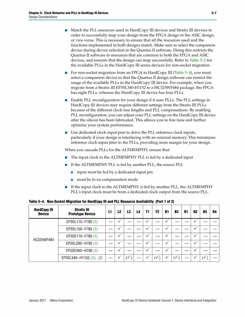
Chapter 5: Clock Networks and PLLs in HardCopy III Devices 5–7Design Considerations
January 2011 Altera Corporation HardCopy III Device Handbook Volume 1: Device Interfaces and Integration
■ Match the PLL resources used in HardCopy III devices and Stratix III devices in order to successfully map your design from the FPGA design to the ASIC design, or vice-versa. This is necessary to ensure that all the resources used and the functions implemented in both designs match. Make sure to select the companion device during device selection in the Quartus II software. Doing this restricts the Quartus II software to resources that are common to both the FPGA and ASIC devices, and ensures that the design can map successfully. Refer to Table 5–2 for the available PLLs in the HardCopy III series devices for non-socket migration.
■ For non-socket migration from an FPGA to HardCopy III (Table 5–4), you must select a companion device so that the Quartus II design software can restrict the usage of the available PLLs in the HardCopy III device. For example, when you migrate from a Stratix III EP3SL340-H1152 to a HC325WF484 package, the FPGA has eight PLLs, whereas the HardCopy III device has four PLLs.
■ Enable PLL reconfiguration for your design if it uses PLLs. The PLL settings in HardCopy III devices may require different settings from the Stratix III PLLs because of the different clock tree lengths and PLL compensations. By enabling PLL reconfiguration, you can adjust your PLL settings on the HardCopy III device after the silicon has been fabricated. This allows you to fine tune and further optimize your system performance.
■ Use dedicated clock input pins to drive the PLL reference clock inputs, particularly if your design is interfacing with an external memory. This minimizes reference clock input jitter to the PLLs, providing more margin for your design.
When you cascade PLLs for the ALTMEMPHY, ensure that:
■ The input clock to the ALTMEMPHY PLL is fed by a dedicated input
■ If the ALTMEMPHY PLL is fed by another PLL, the source PLL
■ input must be fed by a dedicated input pin
■ must be in no compensation mode
■ If the input clock to the ALTMEMPHY is fed by another PLL, the ALTMEMPHY PLL's input clock must be from a dedicated clock output from the source PLL.
Table 5–4. Non-Socket Migration for HardCopy III and PLL Resource Availability (Part 1 of 2)
HardCopy III Device
Stratix III Prototype Device L1 L2 L3 L4 T1 T2 B1 B2 R1 R2 R3 R4
HC325WF484
EP3SL110--F780 (1) — — — — — — — —
EP3SL150--F780 (1) — — — — — — — —
EP3SE110--F780 (1) — — — — — — — —
EP3SL200--H780 (1) — — — — — — — —
EP3SE260--H780 (1) — — — — — — — —
EP3SL340--H1152 (1), (2) — () — () () — () —

5–8 Chapter 5: Clock Networks and PLLs in HardCopy III DevicesDocument Revision History
HardCopy III Device Handbook Volume 1: Device Interfaces and Integration January 2011 Altera Corporation
Document Revision HistoryTable 5–5 lists the revision history for this chapter.
HC325FF484
EP3SL110--F780 (1) — — — — — — — —
EP3SL150--F780 (1) — — — — — — — —
EP3SE110--F780 (1) — — — — — — — —
EP3SL200--H780 (1) — — — — — — — —
EP3SE260--H780 (1) — — — — — — — —
EP3SL340--H1152 (1), (2) — () — () () — () —
HC325WF780 EP3SL340--H1152 (1), (2) — () — () () — () —
HC325FF780 EP3SL340--H1152 (1), (2) — () — () () — () —
Notes to Table 5–4
(1) These are non-socket replacement devices. A board re-design is required.(2) The FPGA has eight available PLLs and the HardCopy III device has four available PLLs.
Table 5–4. Non-Socket Migration for HardCopy III and PLL Resource Availability (Part 2 of 2)
HardCopy III Device
Stratix III Prototype Device L1 L2 L3 L4 T1 T2 B1 B2 R1 R2 R3 R4
Table 5–5. Document Revision History
Date Version Changes
January 2011 3.1
■ Updated Table 5–2 and Table 5–4. Removed device HC315WF484.
■ Used new document template.
■ Minor text edits.
June 2009 3.0 Added non-socket information and new part numbers.
December 2008 2.0 Made minor editorial changes.
May 2008 1.0 Initial release.

March 2012 Altera Corporation HardCopy III Device Handbook Volume 1: Device Interfaces and Integration
Section II. I/O Interfaces
This section includes the following chapters:
■ Chapter 6, I/O Features for HardCopy III Devices
■ Chapter 7, External Memory Interfaces in HardCopy III Devices
■ Chapter 8, High-Speed Differential I/O Interfaces and DPA in HardCopy III Devices
Revision HistoryRefer to each chapter for its own specific revision history. For information on when each chapter was updated, refer to the Chapter Revision Dates section, which appears in the full handbook.
January 2011<edit Part Number variable in chapter>

II–2 Section II: I/O Interfaces
HardCopy III Device Handbook Volume 1: Device Interfaces and Integration March 2012 Altera Corporation
HardCopy III Device Handbook Volume 1: Device Interfaces and IntegrationJanuary 2011
HIII51006-3.1
Subscribe
© 2011 Altera Corporation. All rights reserved. ALTERA, ARRIA, CYCLONE, HARDCOPY, MAX, MEGACORE, NIOS, QUARTUS and STRATIX are Reg. U.S. Pat. & Tm. Off. and/or trademarks of Altera Corporation in the U.S. and other countries. All other trademarks and service marks are the property of their respective holders as described at www.altera.com/common/legal.html. Altera warrants performance of its semiconductor products to current specifications in accordance with Altera’s standard warranty, but reserves the right to make changes to any products and services at any time without notice. Altera assumes no responsibility or liability arising out of the application or use of any information, product, or service described herein except as expressly agreed to in writing by Altera. Altera customers are advised to obtain the latest version of device specifications before relying on any published information and before placing orders for products or services.
6. I/O Features for HardCopy III Devices
This chapter describes the I/O standards, features, termination schemes, and performance supported in HardCopy® III devices. All HardCopy III devices have configurable high-performance I/O drivers and receivers supporting a wide range of industry standard interfaces. Both the top/bottom (column) and left/right (row) I/O banks of HardCopy III devices support the same I/O standards with different performance specifications.
This chapter includes the following sections:
■ “Differences Between HardCopy III ASICs and Stratix III FPGAs” on page 6–2
■ “I/O Standards and Voltage Levels” on page 6–4
■ “HardCopy III I/O” on page 6–7
■ “HardCopy III I/O Banks” on page 6–8
■ “HardCopy III I/O Structure” on page 6–9
■ “MultiVolt I/O Interface” on page 6–9
■ “3.3/3.0-V I/O Interface” on page 6–10
■ “On-Chip Termination Support and I/O Termination Schemes” on page 6–11
■ “OCT Calibration Block Location” on page 6–12
■ “Design Considerations” on page 6–12
Numerous I/O features assist in the high-speed data transfer into and out of the HardCopy device.
HardCopy III devices support the following I/O standards:
■ Single-ended, non-voltage-referenced or voltage-referenced I/O standards
■ Low-voltage differential signaling (LVDS)
■ Reduced swing differential signal (RSDS)
■ Mini-LVDS
■ High-speed transceiver logic (HSTL)
■ Stub series terminated logic (SSTL)
■ Single data rate (SDR) and half data rate (HDR—half the frequency and twice the data width of SDR) input and output options
■ Up to 88 full duplex 1.25 Gbps true LVDS channels (88 Tx + 88 Rx) on the row I/O banks
Features supported in a single-ended I/O interface include:
■ De-skew, read and write leveling, and clock-domain crossing functionality
■ Multiple output current strength setting for different I/O standards
January 2011HIII51006-3.1
6–2 Chapter 6: I/O Features for HardCopy III DevicesDifferences Between HardCopy III ASICs and Stratix III FPGAs
HardCopy III Device Handbook Volume 1: Device Interfaces and Integration January 2011 Altera Corporation
■ Four slew rate settings
■ Four output delay settings
■ Six I/O delay settings
■ Optional bus-hold
■ Optional pull-up resistor
■ Optional open-drain output
■ Serial, parallel, and dynamic on-chip termination (OCT)
Features supported in a high-speed memory interface include:
■ Dedicated DQ strobe (DQS) logic in both column and row I/Os
■ Each I/O bank is accessible by two delay-locked loops (DLLs) that have different frequencies and phase shifts
■ Low-power option when you do not use the memory interface
Features supported in a high-speed differential I/O interface include:
■ Four slew rate settings
■ Differential OCT
■ Hard dynamic phase alignment (DPA) block with serializer/deserializer (SERDES)
■ Four pre-emphasis settings
■ Four differential output voltage (VOD) settings
Differences Between HardCopy III ASICs and Stratix III FPGAs Both HardCopy III and Stratix® III devices support the same speed, performance, I/O standards and implementation guidelines, except I/O standards that require 3.3-V in Stratix III devices. You can prototype I/O interfaces with Stratix III devices and map the design to HardCopy III devices. HardCopy III devices do not support 3.3-V VCCIO due to the device reliability of 40nm process technology. However, HardCopy III devices can interface with a 3.3 V interface. Refer to the section “3.3/3.0-V I/O Interface” on page 6–10 for more information.
You must set the HardCopy III companion device for your Stratix III design project in the Quartus® II software. Otherwise, you may not be able to map to a HardCopy III device due to varying amounts of resource availability. There are four major differences between HardCopy III and Stratix III families:
■ Unlike Stratix III devices, HardCopy III devices require external voltage regulators to regulate VCCIO power from 3.3 V to 3 V for device reliability.
■ There are up to eight calibration blocks in HardCopy III devices instead of up to ten calibration blocks in Stratix III devices.
■ Stratix III devices support up to 24 I/O banks while HardCopy III devices support up to 20 I/O banks.

Chapter 6: I/O Features for HardCopy III Devices 6–3Differences Between HardCopy III ASICs and Stratix III FPGAs
January 2011 Altera Corporation HardCopy III Device Handbook Volume 1: Device Interfaces and Integration
Stratix III and HardCopy III devices support different I/O counts per bank. Therefore, always set the HardCopy III companion device for your Stratix III design project in the Quartus II software. For more information, refer to Table 6–2.
Certain HardCopy III densities may have their speed and timing performance affected when compared with their companion FPGA due to the differences in the architectural layout of the PLLs and I/O pins:
■ I/O pin overhang—refers to some of the vertical I/Os that are located sufficiently away from the HCell core and RAM blocks. This can result in a larger skew when compared with an I/O placed next to the HCell or RAM block. For more information, refer to Figure 6–1, Figure 6–2, and Table 6–1.
■ I/O pin adjacent to the PLL—Some HardCopy III devices have the PLL placed in the core when compared with their companion FPGA, which may have the PLL located in the periphery. In this instance, when using I/Os adjacent to the PLLs in the HardCopy III device, if the source/destination in the HCell is blocked by the PLL, a larger skew may result when compared with the I/Os not located next to the HCell or RAM block.
I/O pin overhang and I/O pin adjacent to the PLL can cause different skew results and timing performance between the FPGA and the HardCopy III device.
1 If your HardCopy III device design has timing closure challenges containing a wide parallel interface with a very tight skew budget, consider avoiding these I/O pins. Instead, use these I/O pins for a slower data rate or as controls.
When migrating from the FPGA to the HardCopy III device, use the Chip Planner in both the FPGA and the HardCopy III device to plan with these I/Os.
Figure 6–1 and Figure 6–2 show the locations of the I/O pin overhang and I/O pin adjacent to the PLL. Use the Chip Planner in the Quartus II software to obtain a more accurate layout of these I/Os.
Figure 6–1. HC325 Devices Not Affected by I/O Pin Overhang and PLL Obstruction
HCell Core
IOEs IOEs
IOEsIOEs PLL
PLLs

6–4 Chapter 6: I/O Features for HardCopy III DevicesI/O Standards and Voltage Levels
HardCopy III Device Handbook Volume 1: Device Interfaces and Integration January 2011 Altera Corporation
Table 6–1 lists the HardCopy III devices that may be affected by architectural differences in your I/O pin layouts.
I/O Standards and Voltage LevelsHardCopy III devices support a wide range of industry I/O standards, including single-ended, voltage-referenced single-ended, and differential I/O standards. Table 6–2 lists the supported I/O standards and the typical values for input and output VCCIO, VCCPD, VREF, and board VTT.
Figure 6–2. HC335 Devices Have a PLL Obstruction Issue for the Top and Bottom I/Os
Table 6–1. I/O Pin Layout for HardCopy III Devices
I/O Pin Layout Differences Devices Affected
Not affected HC325FF484, HC325FF780, HC325WF484, and HC325WF780
VIO overhang None
I/O pins adjacent to the PLL HC335FF1152, HC335LF1152, HC335FF1517, and HC335LF1517
HCell Core
PLL obstructs thedirect signal path
IOEs
IOEs
IOEs
IOEs
IOEs
IOEs
PLLs PLLs
PLLs
PLLs
Table 6–2. I/O Standards and Voltage Levels HardCopy III Devices (Part 1 of 3) (Note 1)
I/O Standard Standard Support
VCCIO(V)VCCPD (V)
(Pre-Driver
Voltage)
VREF (V) (Input Ref
Voltage)
VTT (V) (Board
Termination Voltage)
Input Operation Output Operation
ColumnI/O Banks
Row I/O Banks
Column I/O Banks
Row I/O Banks
3.0-V LVTTL JESD8-B 3.0/2.5 3.0/2.5 3.0 3.0 3.0 — —
3.0-V LVCMOS JESD8-B 3.0/2.5 3.0/2.5 3.0 3.0 3.0 — —
2.5-V LVTTL/ LVCMOS JESD8-5 3.0/2.5 3.0/2.5 2.5 2.5 2.5 — —
1.8-V LVTTL/ LVCMOS JESD8-7 1.8/1.5 1.8/1.5 1.8 1.8 2.5 — —
1.5-V LVTTL/ LVCMOS JESD8-11 1.8/1.5 1.8/1.5 1.5 1.5 2.5 — —
1.2-V LVTTL/ LVCMOS JESD8-12 1.2 1.2 1.2 1.2 2.5 — —
3.0-V PCI (4) PCI Rev 2.2 3.0 3.0 3.0 3.0 3.0 — —
3.0-V PCI-X (4) PCI-X Rev 1.0 3.0 3.0 3.0 3.0 3.0 — —

Chapter 6: I/O Features for HardCopy III Devices 6–5I/O Standards and Voltage Levels
January 2011 Altera Corporation HardCopy III Device Handbook Volume 1: Device Interfaces and Integration
SSTL-2 Class I JESD8-9B (2) (2) 2.5 2.5 2.5 1.25 1.25
SSTL-2 Class II JESD8-9B (2) (2) 2.5 2.5 2.5 1.25 1.25
SSTL-18 Class I JESD8-15 (2) (2) 1.8 1.8 2.5 0.90 0.90
SSTL-18 Class II JESD8-15 (2) (2) 1.8 1.8 2.5 0.90 0.90
SSTL-15 Class I — (2) (2) 1.5 1.5 2.5 0.75 0.75
SSTL-15 Class II (3) — (2) (2) 1.5 — 2.5 0.75 0.75
HSTL-18 Class I JESD8-6 (2) (2) 1.8 1.8 2.5 0.90 0.90
HSTL-18 Class II JESD8-6 (2) (2) 1.8 1.8 2.5 0.90 0.90
HSTL-15 Class I JESD8-6 (2) (2) 1.5 1.5 2.5 0.75 0.75
HSTL-15 Class II (3) JESD8-6 (2) (2) 1.5 — 2.5 0.75 0.75
HSTL-12 Class I JESD8-16A (2) (2) 1.2 1.2 2.5 0.6 0.6
HSTL-12 Class II (3) JESD8-16A (2) (2) 1.2 — 2.5 0.6 0.6
Differential SSTL-2 Class I JESD8-9B (2) (2) 2.5 2.5 2.5 — 1.25
Differential SSTL-2Class II JESD8-9B (2) (2) 2.5 2.5 2.5 — 1.25
Differential SSTL-18 Class I JESD8-15 (2) (2) 1.8 1.8 2.5 — 0.90
Differential SSTL-18 Class II JESD8-15 (2) (2) 1.8 1.8 2.5 — 0.90
Differential SSTL-15 Class I — (2) (2) 1.5 1.5 2.5 — 0.75
Differential SSTL-15 Class II — (2) (2) 1.5 — 2.5 — 0.75
Differential HSTL-18 Class I JESD8-6 (2) (2) 1.8 1.8 2.5 — 0.90
Differential HSTL-18 Class II JESD8-6 (2) (2) 1.8 1.8 2.5 — 0.90
Differential HSTL-15 Class I JESD8-6 (2) (2) 1.5 1.5 2.5 — 0.75
Differential HSTL-15 Class II JESD8-6 (2) (2) 1.5 — 2.5 — 0.75
Differential HSTL-12 Class I JESD8-16A (2) (2) 1.2 1.2 2.5 — 0.60
Differential HSTL-12 Class II JESD8-16A (2) (2) 1.2 — 2.5 — 0.60
LVDS (6) ANSI/TIA/ EIA-644 (2) (2) 2.5 2.5 2.5 — —
RSDS (7), (8) — (2) (2) 2.5 2.5 2.5 — —
Table 6–2. I/O Standards and Voltage Levels HardCopy III Devices (Part 2 of 3) (Note 1)
I/O Standard Standard Support
VCCIO(V)VCCPD (V)
(Pre-Driver
Voltage)
VREF (V) (Input Ref
Voltage)
VTT (V) (Board
Termination Voltage)
Input Operation Output Operation
ColumnI/O Banks
Row I/O Banks
Column I/O Banks
Row I/O Banks

6–6 Chapter 6: I/O Features for HardCopy III DevicesI/O Standards and Voltage Levels
HardCopy III Device Handbook Volume 1: Device Interfaces and Integration January 2011 Altera Corporation
f For detailed electrical characteristics of each I/O standard, refer to the DC and Switching Characteristics of HardCopy III Devices chapter in volume 2 of the HardCopy III Device Handbook.
mini-LVDS (7), (8) — (2) (2) 2.5 2.5 2.5 — —
LVPECL — (5) 2.5 — — 2.5 — —
Notes to Table 6–2:
(1) HardCopy III devices do not support the 3.3-V I/O standard. VCCPD is either 2.5 V or 3.0 V. For a 3.0-V I/O standard, VCCPD = 3.0 V. For 2.5 V and below I/O standards, VCCPD = 2.5 V. However, HardCopy III devices can interface with a 3.3 V interface. For more information, refer to the section “3.3/3.0-V I/O Interface” on page 6–10.
(2) Single-ended HSTL/SSTL, differential SSTL/HSTL, and LVDS input buffers are powered by VCCPD. Row I/O banks support both true differential input buffers and true differential output buffers. Column I/O banks support true differential input buffers, but not true differential output buffers. I/O pins are organized in pairs to support differential standards. Column I/O differential HSTL and SSTL inputs use LVDS differential input buffers without on-chip RD support.
(3) Row I/Os do not support HSTL-12 Class II output, HSTL-15 Class II output, or SSTL-15 Class II output.(4) Column I/O supports PCI/PCI-X with an on-chip clamping diode. Row I/O supports PCI/PCI-X with an external clamping diode.(5) Column I/O banks support LVPECL I/O standards only for input clock operation. Differential clock inputs in column I/O use VCCCLKIN.(6) Column I/O banks support LVDS outputs using two single-ended output buffers and external one-resistor (LVDS_E_1R) and a three-resistor
(LVDS_E_3R) network.(7) Row I/O banks support RSDS and mini-LVDS I/O standards using a dedicated LVDS output buffer without a resistor network.(8) Column I/O banks support RSDS and mini-LVDS I/O standards using two single-ended output buffers with one-resistor (RSDS_E_1R and
mini-LVDS_E_1R) and three-resistor (RSDS_E_3R and mini-LVDS_E_3R) networks.
Table 6–2. I/O Standards and Voltage Levels HardCopy III Devices (Part 3 of 3) (Note 1)
I/O Standard Standard Support
VCCIO(V)VCCPD (V)
(Pre-Driver
Voltage)
VREF (V) (Input Ref
Voltage)
VTT (V) (Board
Termination Voltage)
Input Operation Output Operation
ColumnI/O Banks
Row I/O Banks
Column I/O Banks
Row I/O Banks

Chapter 6: I/O Features for HardCopy III Devices 6–7HardCopy III I/O
January 2011 Altera Corporation HardCopy III Device Handbook Volume 1: Device Interfaces and Integration
HardCopy III I/O HardCopy III devices contain up to 20 I/O banks, as shown in Figure 6–3. Row I/O banks contain true differential input and output buffers and banks with dedicated circuitry to support differential standards at speeds up to 1.25 Gbps.
Figure 6–3. I/O Banks for HardCopy III Devices (Note 1), (2), (3), (4), (5), (6), (7), (8), (9)
Notes to Figure 6–3:
(1) There are 12 I/O banks for the 484-pin package, 16 I/O banks for the 780-pin package, and 20 I/O banks for the 1152- and 1517-pin packages.(2) Differential HSTL and SSTL outputs are not true differential outputs. They use two single-ended outputs with the second output programmed as
inverted.(3) Column I/O differential HSTL and SSTL inputs use LVDS differential input buffers without differential OCT support.(4) Column I/O supports LVDS outputs using single-ended buffers and external resistor networks.(5) Column I/O supports PCI/PCI-X with an on-chip clamping diode. Row I/O supports PCI/PCI-X with an external clamping diode.(6) Differential clock inputs on column I/O use VCCCLKIN. All outputs use the corresponding bank VCCIO.(7) Row I/O supports the dedicated LVDS output buffer.(8) Column I/O banks support LVPECL-only standards for input clock operation.(9) Figure 6–3 is a top view of the silicon die that corresponds to a reverse view for flip chip packages. It is a graphical representation only.(10) Single-ended inputs and outputs are not allowed when true differential IO (DPA and non-DPA) exist in a given I/O bank.
PLL_L1
PLL_L4 PLL_R4
PLL_R1
PLL_L2
PLL_L3
PLL_T2PLL_T1
Ban
k 1A
Bank 8A
Ban
k 1C
Ban
k 2C
Ban
k 2A
Bank 8B Bank 7B Bank 7ABank 7CBank 8C
PLL_B2PLL_B1Bank 3A Bank 3B Bank 4B Bank 4ABank 4CBank 3C
PLL_R2
PLL_R3
Ban
k 6A
Ban
k 6C
Ban
k 5C
Ban
k 5A
I/O banks 8A, 8B & 8C support all single-ended and differential input and output operation
I/O banks 7A, 7B & 7C support all single-ended and differential input and output operation
I/O banks 3A, 3B & 3C support all single-ended and differential input and output operation
I/O banks 4A, 4B & 4C support all single-ended and differential input and output operation
Row I/O banks support LVTTL, LVCMOS, 2.5-V, 1.8-V, 1.5-V, 1.2-V, SSTL-2 Class I & II, SSTL-18 Class I & II, SSTL-15 Class I, HSTL-18 Class I & II, HSTL-15 Class I, HSTL-12 Class I, LVDS, RSDS, mini-LVDS, differential SSTL-2 Class I & II, differential SSTL-18 Class I & II, differential SSTL-15 Class I, differential HSTL-18 Class I & II, differential HSTL-15 Class I and differential HSTL-12 Class I standards for input and output operation.
SSTL-15 class II, HSTL-15 Class II, HSTL-12 Class II, differential SSTL-15 Class II, differential HSTL-15 Class II, differential HSTL-12 Class II standards are only supported for input operations

6–8 Chapter 6: I/O Features for HardCopy III DevicesHardCopy III I/O Banks
HardCopy III Device Handbook Volume 1: Device Interfaces and Integration January 2011 Altera Corporation
Every I/O bank in HardCopy III devices can support high-performance external memory interfaces with dedicated circuitry. The I/O pins are organized in pairs to support differential standards. Each I/O pin pair can support both differential input and output buffers. The only exceptions are the clk1, clk3, clk8, clk10, PLL_L1_clk, PLL_L4_clk, PLL_R1_clk, and PLL_R4_clk pins which support differential input operations only.
f For more information about the number of channels available for the LVDS I/O standard, refer to the High-Speed Differential I/O Interface with DPA in HardCopy III Devices chapter in volume 1 of the HardCopy III Device Handbook.
HardCopy III I/O Banks The I/O pins in HardCopy III devices are arranged in groups called modular I/O banks. Depending on the device package, the number of I/O banks varies. The size of each bank can also vary. Table 6–3 lists the I/O count per bank for all available pin packages.
Table 6–3. I/O Count Per Bank for HardCopy III Devices (Part 1 of 2) (Note 1)
BankDevice Package Pin Count
484 780 1152 1517
1A 24 32 48 50
1C 24 26 42 42
2A 24 32 48 50
2C 24 26 42 42
3A — 40 40 48
3B — — 24 48
3C 24 24 32 32
4A — 40 40 48
4B — — 24 48
4C 24 24 32 32
5A 24 32 48 50
5C 24 26 42 42
6A 24 32 48 50
6C 24 26 42 42
7A — 40 40 48
7B — — 24 48
7C 24 24 32 32
8A — 40 40 48
8B — — 24 48
8C 24 24 32 32
Total Banks 12 16 20 20

Chapter 6: I/O Features for HardCopy III Devices 6–9HardCopy III I/O Structure
January 2011 Altera Corporation HardCopy III Device Handbook Volume 1: Device Interfaces and Integration
HardCopy III I/O Structure The I/O element (IOE) in HardCopy III devices contains a bidirectional I/O buffer and I/O registers to support a complete embedded bidirectional SDR or DDR transfer. Figure 6–3 shows that certain I/O banks support certain I/O standards. The IOEs are located in I/O blocks around the periphery of the HardCopy III device.
The HardCopy III bidirectional IOE also supports features such as:
■ MultiVolt I/O interface
■ Dedicated circuitry for external memory interface
■ Input delay
■ Four output-current strength settings for single-ended I/Os
■ Four slew rate settings for both single-ended and differential I/Os
■ Four output delay settings for single-ended I/Os
■ Six I/O delay settings for single-ended I/Os
■ Optional bus-hold
■ Optional pull-up resistor
■ Optional open-drain output
■ Optional on-chip series termination with or without calibration
■ Optional on-chip parallel termination with calibration
■ Optional on-chip differential termination
■ Optional PCIe clamping diode
MultiVolt I/O Interface The HardCopy III architecture supports the MultiVolt I/O interface feature that allows HardCopy III devices in all packages to interface with systems of different supply voltages.
The VCCIO pins can be connected to a 1.2-, 1.5-, 1.8-, 2.5-, or 3.0-V power supply, depending on the output requirements. The output levels are compatible with systems of the same voltage as the power supply. (For example, when VCCIO pins are connected to a 1.5-V power supply, the output levels are compatible with 1.5-V systems.)
Total I/O Pins 288 488 744 880 (2)
Notes to Table 6–3:
(1) These numbers include dedicated clock pins and regular I/O pins.(2) The HardCopy III F1517-pin package supports less I/O count than the Stratix III F1517-pin package. Therefore, always set HardCopy companion
devices in your Quartus II project to ensure proper mapping.
Table 6–3. I/O Count Per Bank for HardCopy III Devices (Part 2 of 2) (Note 1)
BankDevice Package Pin Count
484 780 1152 1517
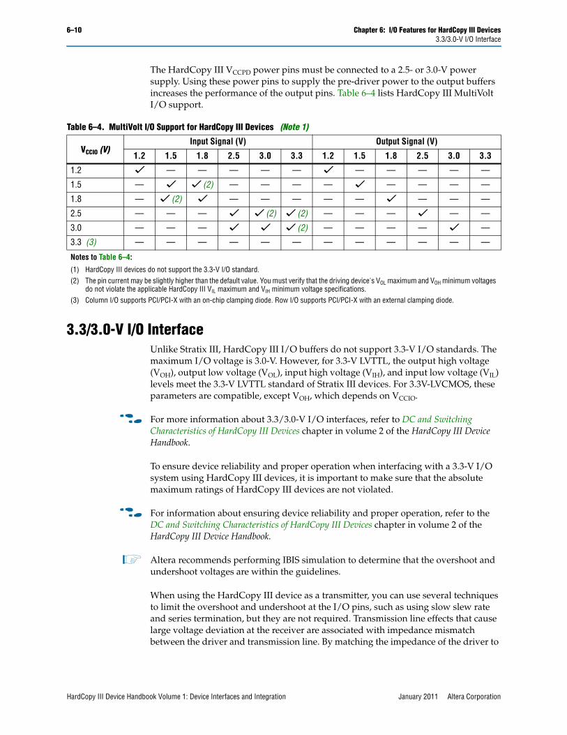
6–10 Chapter 6: I/O Features for HardCopy III Devices3.3/3.0-V I/O Interface
HardCopy III Device Handbook Volume 1: Device Interfaces and Integration January 2011 Altera Corporation
The HardCopy III VCCPD power pins must be connected to a 2.5- or 3.0-V power supply. Using these power pins to supply the pre-driver power to the output buffers increases the performance of the output pins. Table 6–4 lists HardCopy III MultiVolt I/O support.
3.3/3.0-V I/O InterfaceUnlike Stratix III, HardCopy III I/O buffers do not support 3.3-V I/O standards. The maximum I/O voltage is 3.0-V. However, for 3.3-V LVTTL, the output high voltage (VOH), output low voltage (VOL), input high voltage (VIH), and input low voltage (VIL) levels meet the 3.3-V LVTTL standard of Stratix III devices. For 3.3V-LVCMOS, these parameters are compatible, except VOH, which depends on VCCIO.
f For more information about 3.3/3.0-V I/O interfaces, refer to DC and Switching Characteristics of HardCopy III Devices chapter in volume 2 of the HardCopy III Device Handbook.
To ensure device reliability and proper operation when interfacing with a 3.3-V I/O system using HardCopy III devices, it is important to make sure that the absolute maximum ratings of HardCopy III devices are not violated.
f For information about ensuring device reliability and proper operation, refer to the DC and Switching Characteristics of HardCopy III Devices chapter in volume 2 of the HardCopy III Device Handbook.
1 Altera recommends performing IBIS simulation to determine that the overshoot and undershoot voltages are within the guidelines.
When using the HardCopy III device as a transmitter, you can use several techniques to limit the overshoot and undershoot at the I/O pins, such as using slow slew rate and series termination, but they are not required. Transmission line effects that cause large voltage deviation at the receiver are associated with impedance mismatch between the driver and transmission line. By matching the impedance of the driver to
Table 6–4. MultiVolt I/O Support for HardCopy III Devices (Note 1)
VCCIO (V)Input Signal (V) Output Signal (V)
1.2 1.5 1.8 2.5 3.0 3.3 1.2 1.5 1.8 2.5 3.0 3.3
1.2 v — — — — — v — — — — —
1.5 — v v (2) — — — — v — — — —
1.8 — v (2) v — — — — — v — — —
2.5 — — — v v (2) v (2) — — — v — —
3.0 — — — v v v (2) — — — — v —
3.3 (3) — — — — — — — — — — — —
Notes to Table 6–4:
(1) HardCopy III devices do not support the 3.3-V I/O standard.(2) The pin current may be slightly higher than the default value. You must verify that the driving device's VOL maximum and VOH minimum voltages
do not violate the applicable HardCopy III VIL maximum and VIH minimum voltage specifications.(3) Column I/O supports PCI/PCI-X with an on-chip clamping diode. Row I/O supports PCI/PCI-X with an external clamping diode.

Chapter 6: I/O Features for HardCopy III Devices 6–11On-Chip Termination Support and I/O Termination Schemes
January 2011 Altera Corporation HardCopy III Device Handbook Volume 1: Device Interfaces and Integration
the characteristic impedance of the transmission line, you can significantly reduce overshoot voltage. You can use a series termination resistor placed physically close to the driver to match the total driver impedance to transmission line impedance. HardCopy III devices support series on-chip termination (OCT) for all LVTTL/LVCMOS I/O standards in all I/O banks.
When using the HardCopy III device as a receiver, a technique you can use to limit the overshoot, though not required, is using a clamping diode (on-chip or off-chip). HardCopy III devices provide an optional on-chip PCIe clamping diode for column I/O pins. You can use this diode to protect I/O pins against overshoot voltage.
f For more information about absolute maximum rating and maximum allowed overshoot during transitions, refer to the DC and Switching Characteristics of HardCopy III Devices chapter in volume 2 of the HardCopy III Device Handbook.
The following features are identical to those in Stratix III devices:
■ External memory interface
■ High-speed differential I/O with DPA support
■ Four levels of pre-emphasis for LVDS transmitters
■ Four levels of differential output voltage for LVDS transmitters
■ Output current strength
■ Slew rate control
■ Output buffer delay
■ Open-drain output
■ Bus hold
■ Pull-up resistor
f For more information about particular features, refer to the Stratix III Device I/O Features chapter in volume 1 of the Stratix III Device Handbook.
On-Chip Termination Support and I/O Termination SchemesHardCopy III devices support the same termination schemes and on-chip termination (OCT) architecture as Stratix III devices. I/O termination provides impedance matching and helps maintain signal integrity while on-chip termination saves board space and reduces external component costs.
HardCopy III devices support on-chip series termination (RS) with or without calibration, parallel (RT) with calibration, dynamic series and parallel termination for single-ended I/O standards, and on-chip differential termination (RD) for differential LVDS I/O standards.
HardCopy III devices support OCT in all I/O banks by selecting one of the OCT I/O standards. Unlike Stratix III devices, which support up to ten calibration blocks, HardCopy III devices support up to eight OCT calibration blocks.
f For more information about termination schemes for I/O standards, refer to the Stratix III Device I/O Features chapter in volume 1 of the Stratix III Device Handbook.

6–12 Chapter 6: I/O Features for HardCopy III DevicesOCT Calibration Block Location
HardCopy III Device Handbook Volume 1: Device Interfaces and Integration January 2011 Altera Corporation
OCT Calibration Block LocationFigure 6–4 shows the location of OCT calibration blocks in HardCopy III devices.
You can calibrate the I/O banks with any OCT calibration block with the same VCCIO. Also, I/Os are allowed to transmit data during OCT calibration.
f For more information about the OCT calibration modes of operation and their implementation, refer to the Stratix III Device I/O Features chapter in volume 1 of the Stratix III Device Handbook.
Design ConsiderationsWhile HardCopy III devices feature various I/O capabilities for high-performance and high-speed system designs, there are several other considerations that require attention to ensure the success of those designs. These design practices are consistent with the design practices for Stratix III devices.
I/O Banks Restrictions Each I/O bank can simultaneously support multiple I/O standards. The following sections provide guidelines for mixing non-voltage-referenced and voltage-referenced I/O standards in HardCopy III devices.
Figure 6–4. OCT Calibration Block Location in HardCopy III Devices (Note 1)
Note to Figure 6–4:
(1) Figure 6–4 is a top view of the silicon die that corresponds to a reverse view for flip-chip packages. It is a graphical representation only.
Ban
k 8B
Bank 1C
Bank 2C
Ban
k 3B
CB 0 Bank 1A
CB 1 Bank 2A
Ban
k 8A
CB
9 C
B 2
B
ank
3A
Ban
k 7A
CB
7
Ban
k 7B
Ban
k 7C
Ban
k 8C
Ban
k 3C
CB
4
Ban
k 4A
Ban
k 4B
Ban
k 4C
Bank 6C
Bank 5C
Bank 5A CB 5
Bank 6A CB 6
I/O bank with OCTcalibration block
I/O bank without OCTcalibration block

Chapter 6: I/O Features for HardCopy III Devices 6–13Design Considerations
January 2011 Altera Corporation HardCopy III Device Handbook Volume 1: Device Interfaces and Integration
Non-Voltage-Referenced StandardsEach HardCopy III I/O bank has its own VCCIO pins and can be powered by only one VCCIO voltage supply level, either 1.2-, 1.5-, 1.8-, 2.5-, or 3.0-V. An I/O bank can simultaneously support any number of input signals with different I/O standard assignments, as shown in Table 6–4. For example, an I/O bank with a 2.5-V VCCIO setting can support 2.5-V standard inputs and outputs and 3.0-V LVCMOS inputs (not output or bidirectional pins).
For output signals, a single I/O bank supports non-voltage-referenced output signals that are driving at the same voltage as VCCIO. Because an I/O bank can only have one VCCIO value, it can only drive out that one value for non-voltage-referenced signals.
Voltage-Referenced Standards To accommodate voltage-referenced I/O standards, each HardCopy III device’s I/O bank, such as 1A and 1C, supports separate VREF pins feeding its individual VREF bus. You cannot use the VREF pins as generic I/O pins. Thus, if an I/O bank does not use any voltage-referenced I/O standards, the VREF pin for that I/O bank must be tied to VCCIO or GND. Each bank can only have a single VCCIO voltage level and a single VREF voltage level at a given time.
An I/O bank featuring single-ended or differential standards can support voltage-referenced standards as long as all voltage-referenced standards use the same VREF setting.
For performance reasons, voltage-referenced input standards use their own VCCPD level as the power source. This feature allows you to place voltage-referenced input signals in an I/O bank with a VCCIO of 2.5 or below. For example, you can place HSTL-15 input pins in an I/O bank with a 2.5-V VCCIO.
Voltage-referenced bidirectional and output signals must be the same as the I/O bank’s VCCIO voltage. For example, you can only place SSTL-2 output pins in an I/O bank with a 2.5-V VCCIO.
Mixing Voltage-Referenced and Non-Voltage-Referenced Standards An I/O bank can support both non-voltage-referenced and voltage-referenced pins by applying each of the rule sets individually. For example, an I/O bank can support SSTL-18 inputs and 1.8-V inputs and outputs with a 1.8-V VCCIO and a 0.9-V VREF. Similarly, an I/O bank can support 1.5-V standards, 1.8-V inputs (but not outputs), and HSTL and HSTL-15 I/O standards with a 1.5-V VCCIO and 0.75-V VREF.
Non-Socket Replacement and I/O Resource AvailabilityHardCopy III devices offer non-socket replacement of the FPGA devices. Non-socket replacement requires a board re-design. Table 6–5 lists the non-socket replacement options.
f To ensure I/O resource availability, refer to the Mapping Stratix III Device Resources to HardCopy III Devices chapter in volume 2 of the HardCopy III Device Handbook.

6–14 Chapter 6: I/O Features for HardCopy III DevicesDocument Revision History
HardCopy III Device Handbook Volume 1: Device Interfaces and Integration January 2011 Altera Corporation
Document Revision HistoryTable 6–6 lists the revision history for this chapter.
Table 6–5. Non-Socket Replacement I/O Resource Availability for HardCopy III Devices
HardCopy III Device
Stratix III Prototype Device
HardCopy IIII/O Pins
Stratix IIII/O Pins
HardCopy III Full Duplex LVDS
Pairs
Stratix IIIFull Duplex LVDS
Pairs
HC325WF484
EP3SL110--F780 296 488 48 56
EP3SL150--F780 296 488 48 56
EP3SE110--F780 296 488 48 56
EP3SL200--H780 296 488 48 56
EP3SE260--H780 296 488 48 56
EP3SL340--H1152 296 744 48 88
HC325FF484
EP3SL110--F780 296 488 48 56
EP3SL150--F780 296 488 48 56
EP3SE110--F780 296 488 48 56
EP3SL200--H780 296 488 48 56
EP3SE260--H780 296 488 48 56
EP3SL340--H1152 296 744 48 88
HC325WF780 EP3SL340--H1152 392 744 48 88
HC325FF780 EP3SL340--H1152 488 744 56 88
Table 6–6. Document Revision History
Date Version Changes
January 2011 3.1
■ Updated Table 6–5 and Table 6–2.
■ Updated the “Differences Between HardCopy III ASICs and Stratix III FPGAs” section.
■ Added Figure 6–1 and Figure 6–2.
■ Added Table 6–1.
■ Minor text edits.
June 2009 3.0
■ Added Note 10 to Figure 6–1
■ Replaced Note 3 in Table 6–7
■ Added new section “Non-Socket Replacement and I/O Resource Availability” on page 6–21
■ Added Table 6–9
December 2008 2.0
■ Updated “Introduction”
■ Updated “Voltage-Referenced Standards” on page 6–11
■ Made minor editorial changes
May 2008 1.0 Initial release.

HardCopy III Device Handbook Volume 1: Device Interfaces and IntegrationMarch 2012
HIII51007-3.2
Subscribe
© 2012 Altera Corporation. All rights reserved. ALTERA, ARRIA, CYCLONE, HARDCOPY, MAX, MEGACORE, NIOS, QUARTUS and STRATIX are Reg. U.S. Pat. & Tm. Off. and/or trademarks of Altera Corporation in the U.S. and other countries. All other trademarks and service marks are the property of their respective holders as described at www.altera.com/common/legal.html. Altera warrants performance of its semiconductor products to current specifications in accordance with Altera’s standard warranty, but reserves the right to make changes to any products and services at any time without notice. Altera assumes no responsibility or liability arising out of the application or use of any information, product, or service described herein except as expressly agreed to in writing by Altera. Altera customers are advised to obtain the latest version of device specifications before relying on any published information and before placing orders for products or services.
7. External Memory Interfaces inHardCopy III Devices
This chapter describes the hardware features that support high-speed memory interfacing for each double data rate (DDR) memory standard in HardCopy® III devices. HardCopy III devices feature delay-locked loops (DLLs), phase-locked loops (PLLs), dynamic on-chip termination (OCT), read-and-write leveling, and deskew circuitry.
This chapter contains the following sections:
■ “Memory Interfaces Pin Support” on page 7–3
■ “HardCopy III External Memory Interface Features” on page 7–15
Similar to the Stratix® III I/O structure, the HardCopy III I/O structure has been redesigned to provide flexible and high-performance support for existing and emerging external memory standards. These include high-performance DDR memory standards such as DDR3, DDR2, DDR SDRAM, QDRII+, QDRII SRAM, and RLDRAM II.
HardCopy III devices offer the same external memory interface features found in Stratix III devices. These features include DLLs, PLLs, dynamic OCT, trace mismatch compensation, read-and-write leveling, deskew circuitry, half data rate (HDR) blocks, 4- to 36-bit DQ group widths, and DDR external memory support on all sides of the HardCopy III device. HardCopy III devices provide an efficient architecture to quickly and easily fit wide external memory interfaces with the small modular I/O bank structure.
1 HardCopy III devices are designed to support the same I/O standards and implementation guidelines for external memory interfaces as Stratix III devices.
In addition, the Quartus® II timing analysis tool (TimeQuest Timing Analyzer) provides a complete solution for the highest reliable frequency of operation across process, voltage, and temperature (PVT) variations.
1 PLL reconfiguration is not required for AltMEMPHY-based designs. The AltMEMPHY megafunction has an auto calibration feature so implementing PLL reconfiguration does not add value.
f For more information about the ALTMEMPHY megafunction, refer to the External Memory Interface Handbook.
Altera recommends enabling the PLL reconfiguration feature and the DLL phase offset feature (DLL reconfiguration) for HardCopy III devices. Because HardCopy III devices are mask programmed, they cannot be changed after the silicon is fabricated. By implementing these two features, you can perform timing adjustments to improve or resolve timing issues after the silicon is fabricated.
March 2012HIV51007-2.2

7–2 Chapter 7: External Memory Interfaces in HardCopy III Devices
HardCopy III Device Handbook Volume 1: Device Interfaces and Integration March 2012 Altera Corporation
f For information about the clock rate support for Hardcopy III devices, refer to the System Performance Specifications section of the External Memory Interface Handbook.
Figure 7–1 shows a package-bottom view for HardCopy III external memory support.
Figure 7–1. Package-Bottom View for HardCopy III Devices (Note 1), (2), (3)
Notes to Figure 7–1:
(1) The number of I/O banks and PLLs available depend on the device density.(2) Not all HardCopy III devices support I/O banks 1B, 2B, 5B, and 6B.(3) There is only one PLL on each side of the HC325W and HC325F devices. These devices do not support I/O banks 3B, 4B, 7B, and 8B.
DLL08A 8B 8C 7C 7B 7A
1A
1C
2C
2A
3A 3B 3C 4C 4B 4A
5A
5C
6C
6A
PLL_T1 PLL_T2
PLL_L2
PLL_L3
PLL_R2
PLL_R3
PLL_B2PLL_B1
PLL_L1
DLL3
PLL_R1
PLL_R4
DLL2
PLL_L4
DLL1

Chapter 7: External Memory Interfaces in HardCopy III Devices 7–3Memory Interfaces Pin Support
March 2012 Altera Corporation HardCopy III Device Handbook Volume 1: Device Interfaces and Integration
Figure 7–2 shows the memory interface data path that uses all the HardCopy III I/O element (IOE) features.
Memory Interfaces Pin SupportA typical memory interface requires data (D, Q, or DQ), data strobe (DQS and DQSn/CQn), address, command, and clock pins. Some memory interfaces use data mask (DM) pins to enable write masking and QVLD pins to indicate that the read data is ready to be captured. This section describes how HardCopy III devices support these pins.
Figure 7–2. External Memory Interface Data Path Overview (Note 1), (2), (3)
Notes to Figure 7–2:
(1) Each register block can be bypassed.(2) The blocks for each memory interface may differ slightly.(3) These signals may be bidirectional or unidirectional, depending on the memory standard. When bidirectional, the signal is active during both read
and write operations.
DDR OutputRegisters
MemoryHardCopy III ASIC
DLL
DDR Input Registers
Alignment & Synchronization
Registers
Half Data Rate Output Registers
Clock Management & Reset
4n 2nn
n
2n4n
FIFO(2)
DQ (Read)
DQ (Write)
DQS Logic Block
DQS (Read)
Half Data Rate Input Registers
2n
DDR OutputRegisters
Half Data Rate Output Registers
4 2 DQS (Write)
Resynchronization Clock
Alignment Clock
DQS Write Clock
Half-Rate Resynchronization Clock
Half-Rate Clock
AlignmentRegisters
AlignmentRegisters
2n
2
DQ Write Clock

7–4 Chapter 7: External Memory Interfaces in HardCopy III DevicesMemory Interfaces Pin Support
HardCopy III Device Handbook Volume 1: Device Interfaces and Integration March 2012 Altera Corporation
Data and Data Clock/Strobe PinsHardCopy III DDR memory interface read data-strobes or clocks are called DQS pins. Depending on the memory specifications, the DQS pins can be bidirectional single-ended signals (in DDR2 and DDR SDRAM), bidirectional differential signals (DDR3 and DDR2 SDRAM), unidirectional differential signals (in RLDRAM II), or unidirectional complementary signals (QDRII+ and QDRII SRAM). Connect the unidirectional read-and-write data-strobes or clocks to HardCopy III DQS pins.
HardCopy III devices offer differential input buffers for differential read data-strobe/clock operations and provide an independent DQS logic block for each CQn pin for complementary read data-strobe/clock operations. In the HardCopy III pin tables, the differential DQS pin-pairs are denoted as DQS and DQSn pins; the complementary DQS signals are denoted as DQS and CQn pins. DQSn and CQn pins are marked separately in the pin table. Each CQn pin connects to a DQS logic block and the shifted CQn signals go to the negative-edge input registers in the DQ IOE registers.
1 Use differential DQS signaling for DDR2 SDRAM interfaces running higher than 333 MHz.
HardCopy III DDR memory interface data pins are called DQ pins. The DQ pins can be bidirectional signals, as in DDR3, DDR2, and DDR SDRAM, and RLDRAM II common I/O (CIO) interfaces, or unidirectional signals, as in QDRII+, QDRII SRAM, and RLDRAM II separate I/O (SIO) devices. Connect the unidirectional read data signals to HardCopy III DQ pins and the unidirectional write data signals to a DQS/DQ group other than the read DQS/DQ group. Furthermore, the write clocks must be assigned to the DQS/DQSn pins associated with this write DQS/DQ group. Do not use the DQS/CQn pin-pair for write clocks.
1 Using a DQS/DQ group for the write data signals minimizes output skew and allows access to the write leveling circuitry (for DDR3 SDRAM interfaces). These pins also have access to deskewing circuitry that can compensate for delay mismatch between signals on the bus.
Table 7–1 lists the pin connections between a HardCopy III device and an external memory device.
Table 7–1. Memory Interfaces Pin Utilization for HardCopy III Devices (Part 1 of 2)
Pin Description Memory Standard HardCopy III Pin Utilization
Read Data All DQ
Write Data All DQ (1)
Parity, DM, BWSn, NWSn, QVLD, ECC All DQ (1), (2)

Chapter 7: External Memory Interfaces in HardCopy III Devices 7–5Memory Interfaces Pin Support
March 2012 Altera Corporation HardCopy III Device Handbook Volume 1: Device Interfaces and Integration
The DQS and DQ pin locations are fixed in the pin table. Memory interface circuitry is available in every HardCopy III I/O bank. All memory interface pins support the I/O standards required to support DDR3, DDR2, DDR SDRAM, QDRII+, QDRII SRAM, and RLDRAM II devices.
Read Strobes/Clocks
DDR3 SDRAM DDR2 SDRAM (with differential DQS signaling) (3)
RLDRAM IIDifferential DQS/DQSn
DDR2 SDRAM (with single-ended DQS signaling) (3)
DDR SDRAMSingle-ended DQS
QDRII+ SRAM
QDRII SRAMComplementary DQS/CQn
Write Clocks
QDRII+ SRAM (4)
QDRII SRAM (4)
RLDRAM II SIO
Any unused DQS and DQSn pin pairs (1)
Memory Clocks
DDR3 SDRAM
Any unused DQ or DQS pins with DIFFIO_RX capability for the mem_clk[0] and mem_clk_n[0] signals.
Any unused DQ or DQS pins with DIFFOUT capability for the mem_clk[n:1] and mem_clk_n[n:1] signals (where n is greater than or equal to 1).
DDR2 SDRAM (with differential DQS signaling)
Any DIFFIO_RX pins for the mem_clk[0] and mem_clk_n[0] signals.
Any unused DIFFOUT pins for the mem_clk[n:1] and mem_clk_n[n:1] signals (where n is greater than or equal to 1).
DDR2 SDRAM (with single-ended DQS signaling)
DDR SDRAM
RLDRAM II
Any DIFFOUT pins
QDRII+ SRAM (4)
QDRII SRAM (4)Any unused DQSn pin pairs (1)
Notes to Table 7–1:
(1) If the write data signals are unidirectional including the data mask pins, connect them to a separate DQS/DQ group other than the read DQS/DQ group. Connect the write clock to the DQS and DQSn pin-pair associated with that DQS/DQ group. Do not use the DQS and CQn pin-pair as write clocks.
(2) The BWSn, NWSn, and DM pins must be part of the write DQS/DQ group. Parity, QVLD, and ECC pins must be part of the read DQS/DQ group.(3) DDR2 SDRAM supports either single-ended or differential DQS signaling.(4) QDRII+/QDRII SRAM devices typically use the same clock signals for both write and memory clock pins (K/K# clocks) to latch data and address,
and command signals. The clocks must be part of the DQS/DQ group in this case.
Table 7–1. Memory Interfaces Pin Utilization for HardCopy III Devices (Part 2 of 2)
Pin Description Memory Standard HardCopy III Pin Utilization

7–6 Chapter 7: External Memory Interfaces in HardCopy III DevicesMemory Interfaces Pin Support
HardCopy III Device Handbook Volume 1: Device Interfaces and Integration March 2012 Altera Corporation
HardCopy III devices support DQS and DQ signals with DQ bus modes of x4, x8/x9, x16/x18, or x32/x36, although not all devices support DQS bus mode x32/x36. When any of these pins are not used for memory interfacing, you can use them as user I/Os. In addition, you can use any DQSn or CQn pin not used for clocking as DQ (data) pins. Table 7–2 lists pin support per DQS/DQ bus mode, including the DQS and DQSn/CQn pin pair.
You can also use DQS/DQSn pins in some of the x4 groups as RUP/RDN pins (listed in the pin table). You cannot use a x4 DQS/DQ group for memory interfaces if any of its pin members are being used as RUP and RDN pins for OCT calibration. You may use the x8/x9 group that includes this x4 DQS/DQ group, if either of the following circumstances apply:
■ You are not using DM pins with your differential DQS pins
■ You are not using complementary or differential DQS pins
You can do this because a DQS/DQ x8/x9 group is comprised of 12 pins, as the groups are formed by stitching two DQS/DQ groups in x4 mode with six total pins each (Table 7–2). A typical x8 memory interface contains 10 pins, consisting of one DQS, one DM, and eight DQ pins. If you choose your pin assignment carefully, you can use the two extra pins for RUP and RDN. In a DDR3 SDRAM interface, you must use differential DQS, which means that you only have one extra pin. In this case, pick different pin locations for the RUP and RDN pins (for example, in the bank that contains the address and command pins).
You cannot use the RUP and RDN pins shared with DQS/DQ group pins when using x9 QDRII+/QDRII SRAM devices, as the RUP and RDN pins have a dual purpose with the CQn pins. In this case, pick different pin locations for the RUP and RDN pins to avoid conflict with memory interface pin placement. You have the choice of placing the RUP and RDN pins in the data-write group or in the same bank as the address and command pins. There is no restriction for using x16/x18 or x32/x36 DQS/DQ groups that include the x4 groups in which the pin members are used as RUP and RDN pins. These groups contain enough extra pins that they can be used as DQS pins.
Table 7–2. DQS/DQ Bus Mode Pins for HardCopy III Devices (Note 1), (2), (3), (4), (5)
Mode DQSn Support
CQn Support
Parity or DM (Optional)
QVLD (Optional)
Typical Number of Data Pins per
Group
Maximum Number of Data Pins per
Group
x4 Yes No No No 4 5
x8/x9 Yes Yes Yes Yes 8 or 9 11
x16/x18 Yes Yes Yes Yes 16 or 18 23
x32/x36 Yes Yes Yes Yes 32 or 36 47
Notes to Table 7–2:
(1) The QVLD pin is not used in the ALTMEMPHY megafunction.(2) This represents the maximum number of DQ pins (including parity, data mask, and QVLD pins) connected to the DQS bus network with
single-ended DQS signaling. When you use differential or complementary DQS signaling, the maximum number of data per group decreases by one. This number may vary per DQS/DQ group in a particular device. Check the pin table for the accurate number per group.
(3) Two x4 DQS/DQ groups are stitched to make a x8/x9 group, so there are a total of 12 pins in this group.(4) Four x4 DQS/DQ groups are stitched to make a x16/x18 group.(5) Eight x4 DQS/DQ groups are stitched to make a x32/x36 group.
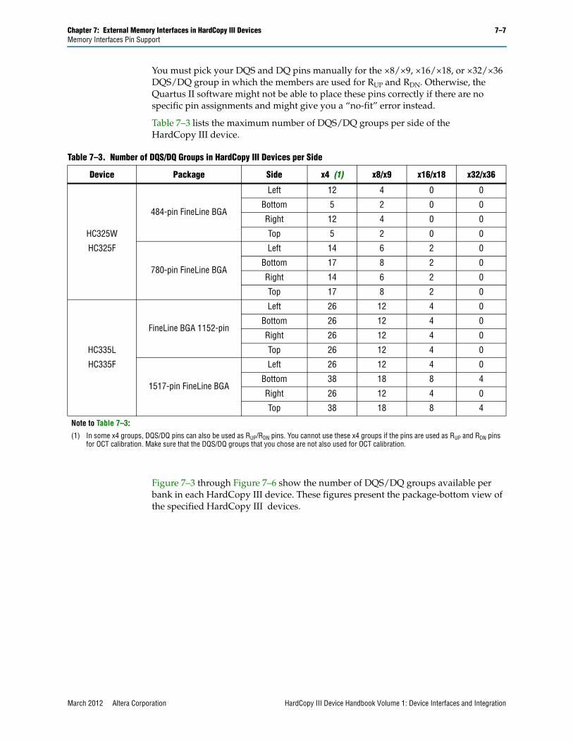
Chapter 7: External Memory Interfaces in HardCopy III Devices 7–7Memory Interfaces Pin Support
March 2012 Altera Corporation HardCopy III Device Handbook Volume 1: Device Interfaces and Integration
You must pick your DQS and DQ pins manually for the ×8/×9, ×16/×18, or ×32/×36 DQS/DQ group in which the members are used for RUP and RDN. Otherwise, the Quartus II software might not be able to place these pins correctly if there are no specific pin assignments and might give you a “no-fit” error instead.
Table 7–3 lists the maximum number of DQS/DQ groups per side of the HardCopy III device.
Figure 7–3 through Figure 7–6 show the number of DQS/DQ groups available per bank in each HardCopy III device. These figures present the package-bottom view of the specified HardCopy III devices.
Table 7–3. Number of DQS/DQ Groups in HardCopy III Devices per Side
Device Package Side x4 (1) x8/x9 x16/x18 x32/x36
HC325W
HC325F
484-pin FineLine BGA
Left 12 4 0 0
Bottom 5 2 0 0
Right 12 4 0 0
Top 5 2 0 0
780-pin FineLine BGA
Left 14 6 2 0
Bottom 17 8 2 0
Right 14 6 2 0
Top 17 8 2 0
HC335L
HC335F
FineLine BGA 1152-pin
Left 26 12 4 0
Bottom 26 12 4 0
Right 26 12 4 0
Top 26 12 4 0
1517-pin FineLine BGA
Left 26 12 4 0
Bottom 38 18 8 4
Right 26 12 4 0
Top 38 18 8 4
Note to Table 7–3:
(1) In some x4 groups, DQS/DQ pins can also be used as RUP/RDN pins. You cannot use these x4 groups if the pins are used as RUP and RDN pins for OCT calibration. Make sure that the DQS/DQ groups that you chose are not also used for OCT calibration.

7–8 Chapter 7: External Memory Interfaces in HardCopy III DevicesMemory Interfaces Pin Support
HardCopy III Device Handbook Volume 1: Device Interfaces and Integration March 2012 Altera Corporation
Figure 7–3. Number of DQS/DQ Groups per Bank in HC4E25W and HC325F Devices in a 484-pin FineLine BGA Package (Note 1), (2)
Notes to Figure 7–3:
(1) These devices do not support ×32/×36 mode.(2) All I/O pin counts include eight dedicated clock inputs (CLK1p, CLK1n, CLK3p, CLK3n, CLK8p, CLK8n, CLK10p, and CLK10n).
DLL 0 DLL 3
I/O Bank 3C
24 User I/Os×4=2
×8/×9=1×16/×18=0
I/O Bank 4C
24 User I/Os×4=3
×8/×9=1×16/×18=0
I/O Bank 2A
24 User I/Os×4=3
×8/×9=1×16/×18=0
I/O Bank 2C
24 User I/Os×4=3
×8/×9=1×16/×18=0
I/O Bank 1C
24 User I/Os×4=3
×8/×9=1×16/×18=0
I/O Bank 1A
24 User I/Os×4=3
×8/×9=1×16/×18=0
DLL 1
I/O Bank 8C
24 User I/Os×4=2
×8/×9=1×16/×18=0
I/O Bank 7C
24 User I/Os×4=3
×8/×9=1×16/×18=0
DLL 2
I/O Bank 6A
24User I/Os×4=0
×8/×9=0×16/×18=0
I/O Bank 6C
24User I/Os×4=0
×8/×9=0×16/×18=0
I/O Bank 5C
24User I/Os×4=0
×8/×9=0×16/×18=0
I/O Bank 5A
24User I/Os×4=0
×8/×9=0×16/×18=0
484-pin FineLine BGA

Chapter 7: External Memory Interfaces in HardCopy III Devices 7–9Memory Interfaces Pin Support
March 2012 Altera Corporation HardCopy III Device Handbook Volume 1: Device Interfaces and Integration
Figure 7–4. Number of DQS/DQ Groups per Bank in HC325W and HC325F Devices in a 780-pin FineLine BGA Package (Note 1)
Notes to Figure 7–4:
(1) These devices do not support ×32/×36 mode.(2) You can use DQS/DQSn pins in some of the ×4 groups as RUP/RDN pins. You cannot use a ×4 group for memory interfaces if two pins in the group
are used as RUP and RDN pins for OCT calibration. You can still use the ×16/×18 groups, including the ×4 groups. However, there are restrictions on using ×8/×9 groups that include these ×4 groups.
(3) All I/O pin counts include eight dedicated clock inputs (CLK1p, CLK1n, CLK3p, CLK3n, CLK8p, CLK8n, CLK10p, and CLK10n).
DLL 0 DLL 3
I/O Bank 8A (2)
40 User I/Os×4=6
×8/×9=3×16/×18=1
I/O Bank 8C
24 User I/Os×4=2
×8/×9=1×16/×18=0
I/O Bank 7C
24 User I/Os×4=3
×8/×9=1×16/×18=0
I/O Bank 7A (2)
40 User I/Os×4=6
×8/×9=3×16/×18=1
I/O Bank 1A (2)
32 User I/Os×4=4
×8/×9=2×16/×18=1
I/O Bank 1C
26 User I/Os (3)×4=3
×8/×9=1×16/×18=0
I/O Bank 2C
26 User I/Os (3)×4=3
×8/×9=1×16/×18=0
I/O Bank 2A (2)
32 User I/Os×4=4
×8/x9=2×16/x18=1
DLL 1
I/O Bank 3A (2)
40 User I/Os×4=6
×8/×9=3×16/×18=1
I/O Bank 3C
24 User I/Os×4=2
×8/×9=1×16/×18=0
I/O Bank 4C
24 User I/Os×4=3
×8/×9=1×16/×18=0
I/O Bank 4A (2)
40 User I/Os×4=6
×8/×9=3×16/×18=1
DLL 2
I/O Bank 6A (2)
32 User I/Os×4=4
×8/×9=2×16/×18=1
I/O Bank 6C
26 User I/Os (3)×4=3
×8/×9=1×16/×18=0
I/O Bank 5C
26 User I/Os (3)×4=3
×8/×9=1×16/×18=0
I/O Bank 5A
32 User I/Os×4=4
×8/×9=2×16/×18=1
780-pin FineLine BGA
(2)
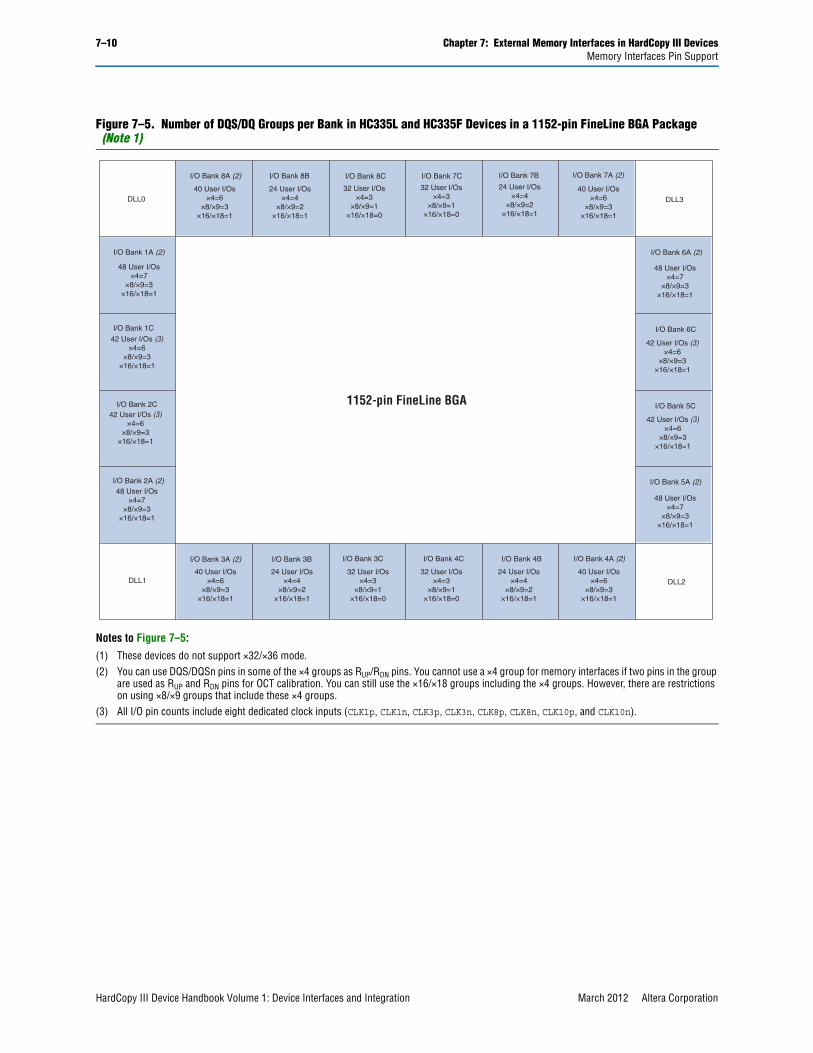
7–10 Chapter 7: External Memory Interfaces in HardCopy III DevicesMemory Interfaces Pin Support
HardCopy III Device Handbook Volume 1: Device Interfaces and Integration March 2012 Altera Corporation
Figure 7–5. Number of DQS/DQ Groups per Bank in HC335L and HC335F Devices in a 1152-pin FineLine BGA Package (Note 1)
Notes to Figure 7–5:
(1) These devices do not support ×32/×36 mode.(2) You can use DQS/DQSn pins in some of the ×4 groups as RUP/RDN pins. You cannot use a ×4 group for memory interfaces if two pins in the group
are used as RUP and RDN pins for OCT calibration. You can still use the ×16/×18 groups including the ×4 groups. However, there are restrictions on using ×8/×9 groups that include these ×4 groups.
(3) All I/O pin counts include eight dedicated clock inputs (CLK1p, CLK1n, CLK3p, CLK3n, CLK8p, CLK8n, CLK10p, and CLK10n).
DLL0 DLL3
DLL1 DLL2
I/O Bank 8A (2)
40 User I/Os×4=6
×8/×9=3×16/×18=1
I/O Bank 8B
24 User I/Os×4=4
×8/×9=2×16/×18=1
I/O Bank 8C
32 User I/Os×4=3
×8/×9=1×16/×18=0
I/O Bank 7C
32 User I/Os×4=3
×8/×9=1×16/×18=0
I/O Bank 7B
24 User I/Os×4=4
×8/×9=2×16/×18=1
I/O Bank 7A (2)
40 User I/Os×4=6
×8/×9=3×16/×18=1
I/O Bank 6A (2)
48 User I/Os×4=7
×8/×9=3×16/×18=1
I/O Bank 6C
42 User I/Os (3)×4=6
×8/×9=3×16/×18=1
I/O Bank 5C
42 User I/Os (3)×4=6
×8/×9=3×16/×18=1
I/O Bank 5A (2)
48 User I/Os×4=7
×8/×9=3×16/×18=1
I/O Bank 4A (2)
40 User I/Os×4=6
×8/×9=3×16/×18=1
I/O Bank 4B
24 User I/Os×4=4
×8/×9=2×16/×18=1
I/O Bank 4C
32 User I/Os×4=3
×8/×9=1×16/×18=0
I/O Bank 3C
32 User I/Os×4=3
×8/×9=1×16/×18=0
I/O Bank 3B
24 User I/Os×4=4
×8/×9=2×16/×18=1
I/O Bank 3A (2)
40 User I/Os×4=6
×8/×9=3×16/×18=1
I/O Bank 2A (2)48 User I/Os
×4=7×8/×9=3
×16/×18=1
I/O Bank 2C42 User I/Os (3)
×4=6×8/×9=3
×16/×18=1
I/O Bank 1C
42 User I/Os (3)×4=6
×8/×9=3×16/×18=1
I/O Bank 1A (2)
48 User I/Os×4=7
×8/×9=3×16/×18=1
1152-pin FineLine BGA

Chapter 7: External Memory Interfaces in HardCopy III Devices 7–11Memory Interfaces Pin Support
March 2012 Altera Corporation HardCopy III Device Handbook Volume 1: Device Interfaces and Integration
The DQS and DQSn pins are listed in the HardCopy III pin tables as DQSXY and DQSnXY, respectively, where X denotes the DQS/DQ grouping number, and Y denotes whether the group is located on the top (T), bottom (B), left (L), or right (R) side of the device.
The corresponding DQ pins are marked as DQXY, where X indicates which DQS group the pins belong to and Y indicates whether the group is located on the top (T), bottom (B), left (L), or right (R) side of the device. For example, DQS1L indicates a DQS pin, located on the left side of the device, as shown in Figure 7–7. The DQ pins belonging to that group are shown as DQ1L in the pin table.
Figure 7–6. Number of DQS/DQ Groups per Bank in HC335L and HC335F Devices in a 1517-pin FineLine BGA Package
Notes to Figure 7–6:
(1) You can use DQS/DQSn pins in some of the ×4 groups as RUP/RDN pins. You cannot use a ×4 group for memory interfaces if two pins in the group are used as RUP and RDN pins for OCT calibration. You can still use the ×16/×18 or ×32/×36 groups including the ×4 groups. However, there are restrictions on using ×8/×9 groups that include these ×4 groups.
(2) All I/O pin counts include eight dedicated clock inputs (CLK1p, CLK1n, CLK3p, CLK3n, CLK8p, CLK8n, CLK10p, and CLK10n) and eight dedicated corner PLL clock inputs (PLL_L1_CLKp, PLL_L1_CLKn, PLL_L4_CLKp, PLL_L4_CLKn, PLL_R4_CLKp, PLL_R4_CLKn, PLL_R1_CLKp, and PLL_R1_CLKn) that can be used for data inputs.
DLL0 DLL3
DLL1 DLL2
I/O Bank 8A (1)
48 User I/Os×4=8
×8/×9=4×16/×18=2×32/×36=1
I/O Bank 8B I/O Bank 8C I/O Bank 7C I/O Bank 7B I/O Bank 7A (1)
I/O Bank 6A (1)
I/O Bank 6C
I/O Bank 5C
I/O Bank 4A (1)I/O Bank 4BI/O Bank 4CI/O Bank 3CI/O Bank 3BI/O Bank 3A (1)
I/O Bank 2C
I/O Bank 1C
I/O Bank 1A (1)
48 User I/Os×4=8
×8/×9=4×16/×18=2×32/×36=1
32 User I/Os×4=3
×8/×9=1×16/×18=0×32/×36=0
32 User I/Os×4=3
×8/×9=1×16/×18=0×32/×36=0
48 User I/Os×4=8
×8/×9=4×16/×18=2×32/×36=1
48 User I/Os×4=8
×8/×9=4×16/×18=2×32/×36=1
50 User I/Os (2)×4=7
×8/×9=3×16/×18=1×32/×36=0
42 User I/Os (2)×4=6
×8/×9=3×16/×18=1×32/×36=0
42 User I/Os (2)×4=6
×8/×9=3×16/×18=1×32/×36=0
48 User I/Os×4=8
×8/×9=4×16/×18=2×32/×36=1
48 User I/Os×4=8
×8/×9=4×16/×18=2×32/×36=1
32 User I/Os×4=3
×8/×9=1×16/×18=0×32/×36=0
32 User I/Os×4=3
×8/×9=1×16/×18=0×32/×36=0
48 User I/Os×4=8
×8/×9=4×16/×18=2×32/×36=1
48 User I/Os×4=8
x8/×9=4×16/×18=2×32/×36=1
50 User I/Os (2)×4=7
×8/×9=3×16/×18=1×32/×36=0
42 User I/Os (2)×4=6
×8/×9=3×16/×18=1×32/×36=0
42 User I/Os (2)×4=6
×8/×9=3×16/×18=1×32/×36=0
I/O Bank 5A (1)
50 User I/Os (2)×4=7
×8/×9=3×16/×18=1×32/×36=0
I/O Bank 2A (1)
50 User I/Os (2)×4=7
×8/×9=3×16/×18=1×32/×36=0
1517-Pin FineLine BGA

7–12 Chapter 7: External Memory Interfaces in HardCopy III DevicesMemory Interfaces Pin Support
HardCopy III Device Handbook Volume 1: Device Interfaces and Integration March 2012 Altera Corporation
Figure 7–7 show how the DQS/DQ groups are numbered in a package-bottom view of the device. The numbering scheme starts from the top left side of the device going counter-clockwise. The top and bottom sides of the HardCopy III device can contain up to 38 x4 DQS/DQ groups; the left and right sides of the device can contain up to 26 x4 DQS/DQ groups.
The parity, DM, BWSn, ECC, and QVLD pins are shown as DQ pins in the pin table. When not used as memory interface pins, these pins are available as regular I/O pins.
The DQ pin numbering is based on ×4 mode. In ×4 mode, there are up to eight DQS/DQ groups per I/O bank. Each ×4 mode DQS/DQ group consists of a DQS pin, a DQSn pin, and four DQ pins. In ×8/×9 mode, the I/O bank combines two adjacent ×4 DQS/DQ groups; one pair of DQS and DQSn/CQn pins can drive all the DQ and parity pins in the new combined group that consists of up to 10 DQ pins (including parity or DM and QVLD pins) and a pair of DQS and DQSn/CQn pins. Similarly, in ×16/×18 mode, the I/O bank combines four adjacent ×4 DQS/DQ groups to create a group with a maximum of 19 DQ pins (including parity or DM and QVLD pins) and a pair of DQS and DQSn/CQn pins. In ×32/×36 mode, the I/O bank combines eight adjacent ×4 DQS/DQ groups together to create a group with a maximum of 37 DQ pins (including parity or DM and QVLD pins) and a pair of DQS and DQSn/CQn pins.
Figure 7–7. DQS Pins in HardCopy III E I/O Banks
DLL0
8A 8B 8C 7C 7B 7A
DQS38T
DQS1L
1A
1C
2C
2A
DQS26L
3A 3B 3C 4C 4B 4A
5A
5C
6C
6A
PLL_T1 PLL_T2
PLL_L2
PLL_L3
PLL_R2
PLL_R3
PLL_B2PLL_B1
DQS13L
PLL_L1
DQS20T DQS19T DQS1T
DQS26R
DQS14R
DQS1R
DQS1B DQS19B DQS20B DQS38B
DQS13RDQS14L
DLL3
PLL_R1
PLL_R4
DLL2
PLL_L4
DLL1

Chapter 7: External Memory Interfaces in HardCopy III Devices 7–13Memory Interfaces Pin Support
March 2012 Altera Corporation HardCopy III Device Handbook Volume 1: Device Interfaces and Integration
HardCopy III modular I/O banks allow easy formation of the DQS/DQ groups. If all the pins in the I/O banks are user I/O pins and are not used for RUP/RDN OCT calibration or PLL clock output pins, you can divide the number of I/O pins in the bank by six to get the maximum possible number of x4 groups. You can then divide that number by two, four, or eight to get the maximum possible number of x8/x9, x16/x18, or x32/x36, respectively, as listed in Table 7–4. However, some of the pins in the I/O bank may be used for other functions.
Optional Parity, DM, BWSn, ECC, and QVLD PinsYou can use any DQ pin from the same DQS/DQ group for data as parity pins in HardCopy III devices. The HardCopy III device family supports parity in the x8/x9, x16/x18, and x32/x36 modes. There is one parity bit available per eight bits of data pins. Use any of the DQ (or D) pins in the same DQS/DQ group as data for parity because parity bits are treated, set, and generated similar to a DQ pin.
DM pins are only required when writing to DDR3, DDR2, DDR SDRAM, and RLDRAM II devices. QDRII+ and QDRII SRAM devices use the BWSn signal to select which byte to write into the memory. A low on the DM or BWSn signals indicates the write is valid. If the DM or BWSn signal is high, the memory masks the DQ signals. If the system does not require write data masking, connect the memory DM pins low to indicate every write data is valid. You can use any of the DQ pins in the same DQS/DQ group as write data for the DM or BWSn signals.
Each group of DQS and DQ signals in DDR3, DDR2, and DDR SDRAM devices requires a DM pin. There is one DM pin per RLDRAM II device and one BWSn pin per nine bits of data in x9, x18, and x36 QDRII+/QDRII SRAM. The ×8 QDRII SRAM device has two BWSn pins per eight data bits, which are referred to as the NWSn pins. Generate the DM or BWSn signals using DQ pins and configure the signals similarly to the DQ (or D) output signals. HardCopy III devices do not support the DM signal in x4 DDR3 SDRAM or in x4 DDR2 SDRAM interfaces with differential DQS signaling.
Table 7–4. DQ/DQS Group in HardCopy III Modular I/O Banks
Modular I/O Bank Size (1)
Maximum Possible Number of x4
Groups
Maximum Possible Number of x8/x9
Groups
Maximum Possible Number of x16/x18
Groups
Maximum Possible Number of x32/x36
Groups
24 pins 4 (2) 2 1 0
32 pins 5 (3) 2 1 0
40 pins 6 3 1 0
48 pins 8 4 2 1
Notes to Table 7–4:
(1) This I/O pin count does not include dedicated clock inputs or the dedicated corner PLL clock inputs.(2) Some of the x4 groups may use the RUP and RDN pins. You cannot use these groups if you use the HardCopy III calibrated OCT feature.(3) The actual maximum number of x4 groups for an I/O bank with 32 pins is four in the HardCopy III devices.
7–14 Chapter 7: External Memory Interfaces in HardCopy III DevicesMemory Interfaces Pin Support
HardCopy III Device Handbook Volume 1: Device Interfaces and Integration March 2012 Altera Corporation
Some DDR3, DDR2, and DDR SDRAM devices or modules support error correction coding (ECC), which is a method of detecting and automatically correcting errors in data transmission. In 72-bit DDR3, DDR2, or DDR SDRAM interfaces, the typical eight ECC pins are used in addition to the 64 data pins. Connect the DDR3, DDR2, and DDR SDRAM ECC pins to a HardCopy III device DQS/DQ group. These signals are also generated similar to DQ pins. The memory controller requires encoding and decoding logic for the ECC data. You can also use the extra byte of data for other error checking methods.
QVLD pins are used in RLDRAM II and QDRII+ SRAM interfaces to indicate the read data availability. There is one QVLD pin per memory device. A high on the QVLD pin indicates that the memory is outputting the data requested. Similar to DQ inputs, this signal is edge-aligned with the read clock signals (CQ/CQn in QDRII+/QDRII SRAM and QK/QK# in RLDRAM II) and is sent half-a-clock cycle before data starts from the memory. The QVLD pin is not used in the ALTMEMPHY solution for QDRII+ SRAM.
For more information about the parity, ECC, and QVLD pins, and when these pins are treated as DQ pins, refer to “Data and Data Clock/Strobe Pins” on page 7–4.
Address and Control/Command PinsAddress and control/command signals are typically sent at single data rate. The only exception is in QDRII SRAM burst-of-two devices, in which case the read address must be captured on the rising edge of the clock and the write address must be captured on the falling edge of the clock by the memory. There is no special circuitry required for the address and control/command pins. You can use any of the user I/O pins in the same I/O bank as the data pins.
Memory Clock PinsIn addition to DQS (and CQn) signals to capture data, DDR3, DDR2, DDR SDRAM, and RLDRAM II use an extra pair of clocks, called CK and CK# signals, to capture the address and control/command signals. The CK and CK# signals must be generated to mimic the write data-strobe using HardCopy III DDR I/O registers (DDIOs) to ensure that the timing relationships between the CK, CK#, and DQS signals (tDQSS in DDR3, DDR2, and DDR SDRAM or tCKDK in RLDRAM II) are met. QDRII+ and QDRII SRAM devices use the same clock (K/K#) to capture the data, address, and control/command signals.
Memory clock pins in HardCopy III devices are generated using a DDIO register going to differential output pins, marked in the pin table with DIFFOUT, DIFFIO_TX, and DIFFIO_RX prefixes. For more information about which pins to use for memory clock pins, refer to Table 7–2 on page 7–6.

Chapter 7: External Memory Interfaces in HardCopy III Devices 7–15HardCopy III External Memory Interface Features
March 2012 Altera Corporation HardCopy III Device Handbook Volume 1: Device Interfaces and Integration
Figure 7–8 shows memory clock generation for HardCopy III devices.
HardCopy III External Memory Interface FeaturesHardCopy III devices are rich with features that allow robust high-performance external memory interfacing. The ALTMEMPHY megafunction allows you to set these external memory interface features and helps set up the physical interface (PHY) best suited for your system.
This section describes each HardCopy III device feature that is used in external memory interfaces from the DQS phase-shift circuitry, DQS logic block, leveling multiplexers, dynamic OCT control block, IOE registers, IOE features, and the PLL.
1 When using the Altera® memory controller MegaCore® functions, the PHY is instantiated for you.
1 The ALTMEMPHY megafunction and the Altera memory controller MegaCore functions can run at half the frequency of the I/O interface of the memory devices to allow better timing management in high-speed memory interfaces. HardCopy III devices have built-in registers to convert data from full-rate (I/O frequency) to half-rate (controller frequency) and vice versa. You can bypass these registers if your memory controller is not running at half the rate of the I/O frequency.
f For more information about the ALTMEMPHY megafunction, refer to the External Memory Interface Handbook.
Figure 7–8. Memory Clock Generation Block Diagram (Note 1)
Notes to Figure 7–8:
(1) For the pin location requirements for these pins, refer to Table 7–1 on page 7–4.(2) The mem_clk[0] and mem_clk_n[0] pins for DDR3, DDR2, and DDR SDRAM interfaces use the I/O input buffer for feedback. For memory
interfaces using a differential DQS input, the input feedback buffer is configured as differential input; for memory interfaces using a single-ended DQS input, the input buffer is configured as a single-ended input. Using a single-ended input feedback buffer requires that VREF is provided to that I/O bank’s VREF pins.
CK or DK or K
QD
QD
System Clock
HardCopy HCells I/O Elements
VCC
CK# or DK# or K#
(2)
(2)

7–16 Chapter 7: External Memory Interfaces in HardCopy III DevicesHardCopy III External Memory Interface Features
HardCopy III Device Handbook Volume 1: Device Interfaces and Integration March 2012 Altera Corporation
DQS Phase-Shift CircuitryThe HardCopy III phase-shift circuitry provides phase shift to the DQS and CQn pins on read transactions when the DQS and CQn pins are acting as input clocks or strobes to the HardCopy III device. The DQS phase-shift circuitry consists of DLLs that are shared between multiple DQS pins and the phase-offset module to further fine-tune the DQS phase shift for different sides of the device. Figure 7–9 shows how the DQS phase-shift circuitry is connected to the DQS and CQn pins in the device.
Figure 7–9. DQS and CQn Pins and DQS Phase-Shift Circuitry
DLL Reference
Clock
DQSPhase-Shift
Circuitry
DQSPin
CQnPin
CQnPin
DQSPin
to IOE
Δt
Δt
Δt
Δt
DQSPhase-Shift
Circuitry
DLL Reference
Clock
DLL Reference
Clock
DQSPin
CQnPin
DQSPin
CQnPin
to IOE to IOE to IOE
ΔtΔt Δt
to IOE
Δt
DQS LogicBlocks
DQSPin
CQnPin
CQnPin
DQSPin
to IOE to IOEto IOEto IOE
ΔtΔtΔtΔt
DQSPin
CQnPin
DQSPin
CQnPin
Δt
Δt
Δt
Δt
DQS LogicBlocks
DLL Reference
Clock
DQSPhase-Shift
Circuitry
to IOE
to IOE
to IOE
DQSPhase-Shift
Circuitry
to IOE
to IOE
to IOE
to IOE

Chapter 7: External Memory Interfaces in HardCopy III Devices 7–17HardCopy III External Memory Interface Features
March 2012 Altera Corporation HardCopy III Device Handbook Volume 1: Device Interfaces and Integration
The DQS phase-shift circuitry is connected to the DQS logic blocks that control each DQS or CQn pin. The DQS logic blocks allow the DQS delay settings to be updated concurrently at every DQS or CQn pin.
DLLDQS phase-shift circuitry uses a DLL to dynamically measure the clock period required by the DQS/CQn pin. The DLL, in turn, uses a frequency reference to generate dynamically controlled signals for the delay chains in each of the DQS and CQn pins, allowing it to compensate for PVT variations. The DQS delay settings are Gray-coded to reduce jitter when the DLL updates the settings. The phase-shift circuitry requires a maximum of 1,280 clock cycles to calculate the correct input clock period. Do not send data during these clock cycles because there is no guarantee that it will be captured properly. Because the settings from the DLL may not be stable until this lock period has elapsed, anything using these settings (including the leveling delay system) may be unstable during this period.
1 You can still use the DQS phase-shift circuitry for any memory interfaces that are less than 100 MHz. The DQS signal is shifted by 2.5 ns. Even if the DQS signal is not shifted exactly to the middle of the DQ valid window, the IOE must be able to capture the data in low frequency applications where a large amount of timing margin is available.
There are four DLLs in a HardCopy III device, located in each corner of the device. These four DLLs can support a maximum of four unique frequencies, with each DLL running at one frequency. Each DLL can have two outputs with different phase offsets, allowing one HardCopy III device to have eight different DLL phase shift settings. Figure 7–10 shows the DLL and I/O bank locations in HardCopy III devices, from a package-bottom view.
Altera recommends enabling the PLL reconfiguration feature and the DLL phase offset feature (DLL reconfiguration) for HardCopy III devices. Because HardCopy III devices are mask programmed, they cannot be changed after the silicon is fabricated. By implementing these two features, you can perform timing adjustments to improve or resolve timing issues after the silicon is fabricated.
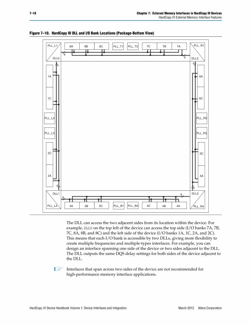
7–18 Chapter 7: External Memory Interfaces in HardCopy III DevicesHardCopy III External Memory Interface Features
HardCopy III Device Handbook Volume 1: Device Interfaces and Integration March 2012 Altera Corporation
The DLL can access the two adjacent sides from its location within the device. For example, DLL0 on the top left of the device can access the top side (I/O banks 7A, 7B, 7C, 8A, 8B, and 8C) and the left side of the device (I/O banks 1A, 1C, 2A, and 2C). This means that each I/O bank is accessible by two DLLs, giving more flexibility to create multiple frequencies and multiple-types interfaces. For example, you can design an interface spanning one side of the device or two sides adjacent to the DLL. The DLL outputs the same DQS delay settings for both sides of the device adjacent to the DLL.
1 Interfaces that span across two sides of the device are not recommended for high-performance memory interface applications.
Figure 7–10. HardCopy III DLL and I/O Bank Locations (Package-Bottom View)
PLL_T1 PLL_T2
PLL_B1 PLL_B2
8A 8B 8C 7C 7B 7A
3A 3B 3C 4C 4B 4A
2A
2C
PLL_L3
PLL_L2
1C
1A
PLL_R3
PLL_R2
5A
5C
6C
6A
66
6
6
6
6
6
6
DLL0
PLL_L1
DLL3
PLL_R1
DLL2
PLL_R4
DLL1
PLL_L4

Chapter 7: External Memory Interfaces in HardCopy III Devices 7–19HardCopy III External Memory Interface Features
March 2012 Altera Corporation HardCopy III Device Handbook Volume 1: Device Interfaces and Integration
Each bank can use settings from either or both DLLs of the adjacent bank. For example, DQS1L can use phase-shift settings from DLL0, and DQS2L can use phase-shift settings from DLL1. Table 7–5 lists the DLL location and supported I/O banks for HardCopy III devices.
1 You can only have one memory interface in I/O banks with the same I/O bank number (such as I/O banks 1A and 1C) when you use the leveling delay chains because there is only one leveling delay chain shared by these I/O banks.
The reference clock for each DLL may come from the PLL output clocks or any of the two dedicated clock input pins located in either side of the DLL. Table 7–6 through Table 7–8 show the available DLL reference clock input resources for HardCopy III devices.
Table 7–5. DLL Location and Supported I/O Banks
DLL Location Accessible I/O Banks
DLL0 Top left corner 1A, 1C, 2A, 2C, 7A, 7B, 7C, 8A, 8B, 8C
DLL1 Bottom left corner 1A, 1C, 2A, 2C, 3A, 3B, 3C, 4A, 4B, 4C
DLL2 Bottom right corner 3A, 3B, 3C, 4A, 4B, 4C, 5A, 5C, 6A, 6C
DLL3 Top right corner 5A, 5C, 6A, 6C, 7A, 7B, 7C, 8A, 8B, 8C
Table 7–6. DLL Reference Clock Input for HC325W, and HC325F Devices
DLL CLKIN (Top/Bottom) CLKIN (Left/Right) PLL (Top/Bottom) PLL (Left/Right)
DLL0 CLK12P, CLK13P, CLK14P, CLK15P CLK0P, CLK1P, CLK2P, CLK3P PLL_T1 PLL_L2
DLL1 CLK4P, CLK5P, CLK6P, CLK7P CLK0P, CLK1P, CLK2P, CLK3P PLL_B1 PLL_L2
DLL2 CLK4P, CLK5P, CLK6P, CLK7P CLK8P, CLK9P, CLK10P, CLK11P PLL_B1 PLL_R2
DLL3 CLK12P, CLK13P, CLK14P, CLK15P CLK8P, CLK9P, CLK10P, CLK11P PLL_T1 PLL_R2
Table 7–7. DLL Reference Clock Input for HC335L and HC335F with F1152-Pin Package Devices
DLL CLKIN (Top/Bottom) CLKIN (Left/Right) PLL (Top/Bottom) PLL (Left/Right)
DLL0 CLK12P, CLK13P, CLK14P, CLK15P CLK0P, CLK1P, CLK2P, CLK3P PLL_T1 PLL_L2
DLL1 CLK4P, CLK5P, CLK6P, CLK7P CLK0P, CLK1P, CLK2P, CLK3P PLL_B1 PLL_L3
DLL2 CLK4P, CLK5P, CLK6P, CLK7P CLK8P, CLK9P, CLK10P, CLK11P PLL_B2 PLL_R3
DLL3 CLK12P, CLK13P, CLK14P, CLK15P CLK8P, CLK9P, CLK10P, CLK11P PLL_T2 PLL_R2
Table 7–8. DLL Reference Clock Input for HC335L and HC335F with F1517-Pin Package Devices
DLL CLKIN (Top/Bottom) CLKIN (Left/Right) PLL (Top/Bottom) PLL (Left/Right)
DLL0 CLK12P, CLK13P, CLK14P, CLK15P CLK0P, CLK1P, CLK2P, CLK3P PLL_T1 PLL_L1, PLL_L2
DLL1 CLK4P, CLK5P, CLK6P, CLK7P CLK0P, CLK1P, CLK2P, CLK3P PLL_B1 PLL_L3, PLL_L4
DLL2 CLK4P, CLK5P, CLK6P, CLK7P CLK8P, CLK9P, CLK10P, CLK11P PLL_B2 PLL_R3, PLL_R4
DLL3 CLK12P, CLK13P, CLK14P, CLK15P CLK8P, CLK9P, CLK10P, CLK11P PLL_T2 PLL_R1, PLL_R2

7–20 Chapter 7: External Memory Interfaces in HardCopy III DevicesHardCopy III External Memory Interface Features
HardCopy III Device Handbook Volume 1: Device Interfaces and Integration March 2012 Altera Corporation
When you have a dedicated PLL that only generates the DLL input reference clock, set the PLL mode to No Compensation; otherwise, the Quartus II software changes it automatically. Because the PLL does not use any other outputs, it does not have to compensate for any clock paths.
Figure 7–11 shows a block diagram of the DLL. The input reference clock goes into the DLL to a chain of up to 16 delay elements. The phase comparator compares the signal coming out of the end of the delay chain block to the input reference clock. The phase comparator then issues the upndn signal to the Gray-code counter. This signal increments or decrements a six-bit delay setting (DQS delay settings) that increases or decreases the delay through the delay element chain to bring the input reference clock and the signals coming out of the delay element chain in phase.
The DLL can be reset from either the core array or a user I/O pin. Each time the DLL is reset, you must wait for 1,280 clock cycles before you can capture the data properly.
Depending on the DLL frequency mode, the DLL can shift the incoming DQS signals by 0°, 22.5°, 30°, 36°, 45°, 60°, 67.5°, 72°, 90°, 108°, 120°, 135°, 144°, or 180°. The shifted DQS signal is then used as the clock for the DQ IOE input registers.
Figure 7–11. Simplified Diagram of the DQS Phase Shift Circuitry (Note 1)
Notes to Figure 7–11:
(1) All features of the DQS phase-shift circuitry are accessible from the ALTMEMPHY MegaWizard Plug-In Manager in the Quartus II software.(2) For exact PLL and input clock pin information, the input reference clock for the DQS phase-shift circuitry can come from a PLL output clock or an
input clock pin. For more information, refer to Table 7–6 through Table 7–8.(3) Phase offset settings can go only to the DQS logic blocks.(4) DQS delay settings can go to the core array, the DQS logic block, and the leveling circuitry.
6
6
6
PhaseOffsetControl
6
Phase offset settingsfrom the core array
Phase offsetsettings to DQS pinson top or bottom edge (3)
DQS DelaySettings (4)
Input ReferenceClock (2) upndn
clock enable
DLL
6
addnsub_a
PhaseComparator
Delay Chains
Up/DownCounter
6
PhaseOffsetControl
Phase offset settingsfrom the core array
Phase offsetsettings to DQS pin on left or right edge (3)
6
addnsub_b

Chapter 7: External Memory Interfaces in HardCopy III Devices 7–21HardCopy III External Memory Interface Features
March 2012 Altera Corporation HardCopy III Device Handbook Volume 1: Device Interfaces and Integration
All DQS and CQn pins referenced to the same DLL can have their input signal phase shifted by a different degree amount, but all must be referenced at one particular frequency. For example, you can have a 90° phase shift on DQS1T and a 60° phase shift on DQS2T referenced from a 200-MHz clock. However, not all phase-shift combinations are supported. The phase shifts on the DQS pins referenced by the same DLL must all be a multiple of 22.5° (up to 90°), a multiple of 30° (up to 120°), a multiple of 36° (up to 144°), or a multiple of 45° (up to 180°).
There are seven different frequency modes for the HardCopy III DLL, as shown in Table 7–9. Each frequency mode provides different phase shift selections. In frequency modes 0, 1, 2, and 3, the 6-bit DQS delay settings vary with PVT to implement the phase-shift delay. In frequency modes 4, 5, and 6, only 5 bits of the DQS delay settings vary to implement the phase-shift delay; the MSB of the DQS delay setting is set to 0.
f For the frequency range of each mode, refer to the DC and Switching Characteristics of HardCopy III Devices chapter.
For the 0° shift, the DQS signal bypasses both the DLL and the DQS logic blocks. The Quartus II software automatically sets the DQ input delay chains so that the skew between the DQ and DQS pin at the DQ IOE registers is negligible when the 0° shift is implemented. You can feed the DQS delay settings to the DQS logic block and the core array.
The shifted DQS signal goes to the DQS bus to clock the IOE input registers of the DQ pins. The signal can also go into the core array for resynchronization if you are not using the IOE resynchronization registers. The shifted CQn signal can only go to the negative-edge input register in the DQ IOE and is only used for QDRII+ and QDRII SRAM interfaces.
Phase Offset ControlEach DLL has two phase-offset modules and can provide two separate DQS delay settings with independent offset, one for the top and bottom I/O banks and one for the left and right I/O banks, so you can fine-tune the DQS phase shift settings between two different sides of the device. Even though you have an independent phase offset control, the frequency of the interface using the same DLL must be the same. Use the phase offset control module for making small shifts to the input signal
Table 7–9. DLL Frequency Modes in HardCopy III Devices
Frequency Mode DQS Delay Setting Bus Width Available Phase Shift Number of Delay
Chains
0 6 bits 22.5°, 45°, 67.5°, 90° 16
1 6 bits 30°, 60°, 90°, 120° 12
2 6 bits 36°, 72°, 108°, 144° 10
3 6 bits 45°, 90°, 135°, 180° 8
4 5 bits 30°, 60°, 90°, 120° 12
5 5 bits 36° 72°, 108°, 144° 10
6 5 bits 45°, 90°, 135°, 180° 8

7–22 Chapter 7: External Memory Interfaces in HardCopy III DevicesHardCopy III External Memory Interface Features
HardCopy III Device Handbook Volume 1: Device Interfaces and Integration March 2012 Altera Corporation
and use the DQS phase-shift circuitry for larger signal shifts. For example, if the DLL only offers a multiple of a 30° phase shift, but your interface requires a 67.5° phase shift on the DQS signal, you can use two delay chains in the DQS logic blocks to give you a 60° phase shift and use the phase offset control feature to implement the extra 7.5° phase shift.
You can use either a static phase offset or a dynamic phase offset to implement the additional phase shift. The available additional phase shift is implemented in 2’s-complement in Gray-code between settings –64 to +63 for frequency modes 0, 1, 2, and 3, and between settings –32 to +31 for frequency modes 4, 5, and 6. The DQS phase shift is the sum of the DLL delay settings and the user selected phase offset settings, which reaches a maximum at setting 64 for mode frequency modes 0, 1, 2 and 3, and a maximum at setting 32 for frequency modes 4, 5, and 6. The actual physical offset setting range is 64 or 32 subtracted by the DQS delay settings from the DLL.
You must monitor the DQS delay settings to determine how many offsets you can add and subtract in the system.
1 The DQS delay settings output by the DLL are also Gray-coded.
For example, if the DLL determines that a DQS delay setting of 28 is required to achieve a 30° phase shift in DLL frequency mode 1, you can subtract up to 28 phase offset settings and add up to 35 phase offset settings to achieve the optimal delay that you need. However, if the same DQS delay setting of 28 is required to achieve a 30° phase shift in DLL frequency mode 4, you can still subtract up to 28 phase offset settings, but you can only add up to 3 phase offset settings before the DQS delay settings reach their maximum settings. This is because DLL frequency mode 4 only uses 5-bit DLL delay settings.
f For information about the value for each step, refer to the DC and Switching Characteristics of HardCopy III Devices chapter.
If you use the static phase offset, specify the phase-offset amount in the ALTMEMPHY megafunction as a positive number for addition or a negative number for subtraction. You can also have a dynamic phase offset that is always added to, subtracted from, or both added to and subtracted from the DLL phase shift. When you always add or subtract, you can dynamically input the phase offset amount into the dll_offset[5..0] port. When you want to both add and subtract dynamically, you control the addnsub signal in addition to the dll_offset[5..0] signals.
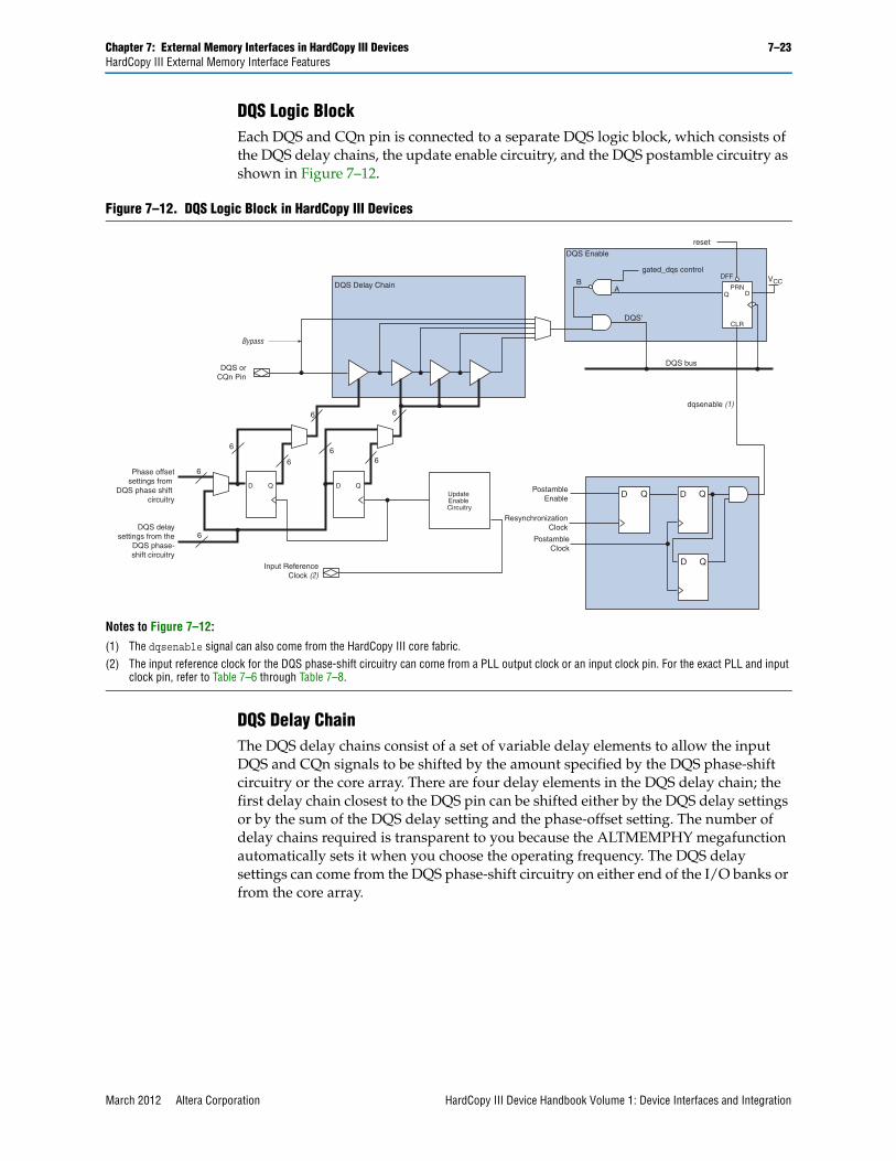
Chapter 7: External Memory Interfaces in HardCopy III Devices 7–23HardCopy III External Memory Interface Features
March 2012 Altera Corporation HardCopy III Device Handbook Volume 1: Device Interfaces and Integration
DQS Logic BlockEach DQS and CQn pin is connected to a separate DQS logic block, which consists of the DQS delay chains, the update enable circuitry, and the DQS postamble circuitry as shown in Figure 7–12.
DQS Delay ChainThe DQS delay chains consist of a set of variable delay elements to allow the input DQS and CQn signals to be shifted by the amount specified by the DQS phase-shift circuitry or the core array. There are four delay elements in the DQS delay chain; the first delay chain closest to the DQS pin can be shifted either by the DQS delay settings or by the sum of the DQS delay setting and the phase-offset setting. The number of delay chains required is transparent to you because the ALTMEMPHY megafunction automatically sets it when you choose the operating frequency. The DQS delay settings can come from the DQS phase-shift circuitry on either end of the I/O banks or from the core array.
Figure 7–12. DQS Logic Block in HardCopy III Devices
Notes to Figure 7–12:
(1) The dqsenable signal can also come from the HardCopy III core fabric.(2) The input reference clock for the DQS phase-shift circuitry can come from a PLL output clock or an input clock pin. For the exact PLL and input
clock pin, refer to Table 7–6 through Table 7–8.
D QD QUpdate Enable Circuitry
6 666
6 6
DQS delaysettings from the
DQS phase-shift circuitry
DQS orCQn Pin
Input ReferenceClock (2)
DQS Delay Chain
Bypass
Phase offsetsettings from
DQS phase shift circuitry
6
6
DQS Enable
gated_dqs control
DQS bus
PRN
CLR
Q
DFF
reset
AB VCC
DQS'
D
PostambleEnable
ResynchronizationClock
PostambleClock
dqsenable (1)
D
D D
Q
Q Q

7–24 Chapter 7: External Memory Interfaces in HardCopy III DevicesHardCopy III External Memory Interface Features
HardCopy III Device Handbook Volume 1: Device Interfaces and Integration March 2012 Altera Corporation
The delay elements in the DQS logic block have the same characteristics as the delay elements in the DLL. When the DLL does not control the DQS delay chains, you can input your own Gray-coded 6-bit or 5-bit settings using the dqs_delayctrlin[5..0] signals available in the ALTMEMPHY megafunction. These settings control 1, 2, 3, or all 4 delay elements in the DQS delay chains. The ALTMEMPHY megafunction can also dynamically choose the number of DQS delay chains required for the system. The amount of delay is equal to the sum of the delay element’s intrinsic delay and the product of the number of delay steps and the value of the delay steps.
You can also bypass the DQS delay chain to achieve a 0° phase shift.
f For more information about the ALTMEMPHY megafunction, refer to the External Memory Interface Handbook.
Update Enable CircuitryBoth the DQS delay settings and the phase-offset settings pass through a register before entering the DQS delay chains. The registers are controlled by the update enable circuitry to allow enough time for changes in the DQS delay setting bits to arrive at all the delay elements. This allows them to be adjusted at the same time. The update enable circuitry enables the registers to allow enough time for the DQS delay settings to travel from the DQS phase-shift circuitry or core logic to all the DQS logic blocks before the next change. It uses the input reference clock or a user clock from the core to generate the update enable output. The ALTMEMPHY megafunction uses this circuit by default. Figure 7–13 shows an example waveform of the update enable circuitry output.
DQS Postamble CircuitryFor external memory interfaces that use a bidirectional read strobe such as DDR3, DDR2, and DDR SDRAM, the DQS signal is low before going to or coming from a high-impedance state. The state where DQS is low, just after a high-impedance state, is called the preamble state; the state where DQS is low, just before it returns to a high-impedance state, is called the postamble state. There are preamble and postamble specifications for both read and write operations in DDR3, DDR2, and DDR SDRAM.
Figure 7–13. DQS Update Enable Waveform
Update Enable Circuitry Output
System Clock
DQS Delay Settings(Updated every 8 cycles)
DLL Counter Update(Every 8 cycles)
6 bit
DLL Counter Update(Every 8 cycles)

Chapter 7: External Memory Interfaces in HardCopy III Devices 7–25HardCopy III External Memory Interface Features
March 2012 Altera Corporation HardCopy III Device Handbook Volume 1: Device Interfaces and Integration
The DQS postamble circuitry, shown in Figure 7–14, ensures that data is not lost when there is noise on the DQS line at the end of a read postamble time. HardCopy III devices have a dedicated postamble register that can be controlled to ground the shifted DQS signal used to clock the DQ input registers at the end of a read operation. This ensures that any glitches on the DQS input signals at the end of the read postamble time do not affect the DQ IOE registers.
In addition to the dedicated postamble register, HardCopy III devices also have an HDR block inside the postamble enable circuitry. These registers are used if the controller is running at half the frequency of the I/Os.
Using the HDR block as the first stage capture register in the postamble enable circuitry block in Figure 7–14 is optional. The HDR block is clocked by the half-rate resynchronization clock, which is the output of the I/O clock divider circuit (shown in Figure 7–20). The AND gate after the postamble register outputs is used to avoid postamble glitches from a previous read burst on a non-consecutive read burst. This scheme allows a half-a-clock cycle latency for dqsenable assertion and zero latency for dqsenable deassertion, as shown in Figure 7–15.
Figure 7–14. DQS Postamble Circuitry in HardCopy III Devices
DQS Enable
gated_dqs control
DQS Bus
PRN
CLR
Q
DFF
reset
AB VCC
DQS'
D
PostambleEnable
ResynchronizationClock
PostambleClock
D
D D
Q
Q Qdqsenable

7–26 Chapter 7: External Memory Interfaces in HardCopy III DevicesHardCopy III External Memory Interface Features
HardCopy III Device Handbook Volume 1: Device Interfaces and Integration March 2012 Altera Corporation
Leveling CircuitryDDR3 SDRAM unbuffered modules use a fly-by clock distribution topology for better signal integrity. This means that the CK/CK# signals arrive at each DDR3 SDRAM device in the module at different times. The difference in arrival time between the first DDR3 SDRAM device and the last device on the module can be as long as 1.6 ns. Figure 7–16 shows the clock topology in DDR3 SDRAM unbuffered modules.
Figure 7–15. Avoiding Glitch on a Non-Consecutive Read Burst Waveform
Delayed by 1/2T logic
PreamblePostamble
Postamble glitch
DQS
Postamble Enable
dqsenable
Figure 7–16. DDR3 SDRAM Unbuffered Module Clock Topology
DQS/DQ DQS/DQDQS/DQDQS/DQDQS/DQ DQS/DQ CK/CK#
HardCopy III
DQS/DQ DQS/DQ

Chapter 7: External Memory Interfaces in HardCopy III Devices 7–27HardCopy III External Memory Interface Features
March 2012 Altera Corporation HardCopy III Device Handbook Volume 1: Device Interfaces and Integration
Because the data and read strobe signals are still point-to-point, special consideration must be taken to ensure that the timing relationship between the CK/CK# and DQS signals (tDQSS) during a write is met at every device on the modules. Furthermore, read data returning to the HardCopy III ASIC from the memory is also staggered in a similar way. HardCopy III ASICs have leveling circuitry to compensate for the different CK/CK# arrival time at each device in the memory module.
There is one group of leveling circuitry per I/O bank, with the same I/O number (for example, there is one leveling circuitry shared between I/O bank 1A and 1C) located in the middle of the I/O bank. These delay chains are PVT-compensated by the same DQS delay settings as the DLL and DQS delay chains. The generated clock phases are distributed to every DQS logic block that is available in the I/O bank. The delay chain taps, then feeds a multiplexer controlled by the ALTMEMPHY megafunction to select which clock phases are to be used for that ×4 or ×8 DQS group. Each group can use a different tap output from the read-leveling and write-leveling delay chains to compensate for the different CK/CK# delay going into each device on the module.
Figure 7–17 and Figure 7–18 show the HardCopy III read-and-write leveling circuitry.
The –90° write clock of the ALTMEMPHY megafunction feeds the write-leveling circuitry to produce the clock to generate the DQS and DQ signals. During initialization, the ALTMEMPHY megafunction picks the correct write-leveled clock for the DQS and DQ clocks for each DQS/DQ group after sweeping all the available clocks in the write calibration process. The DQ clock output is –90° phase-shifted compared to the DQS clock output.
Figure 7–17. Write-Leveling Delay Chains for HardCopy III Devices (Note 1)
Note to Figure 7–17:
(1) There is only one leveling delay chain per I/O bank with the same I/O number (for example, I/O banks 1A and 1C). You can only have one memory controller in these I/O banks when you use the leveling delay chains.
Figure 7–18. Read-Leveling Delay Chains and Multiplexers for HardCopy III Devices (Note 1)
Note to Figure 7–18:
(1) There is only one leveling delay chain per I/O bank with the same I/O number (for example, I/O banks 1A and 1C). You can only have one memory controller in these I/O banks when you use the leveling delay chains.
Write clk(-900) Write-Leveled DQS Clock
Write-Leveled DQ Clock
DQS
Resynchronization clock
Half-Rate Resynchronization Clock
Read-Leveled Resynchronization Clock
I/O Clock Divider
Half-Rate Source Synchronous Clock
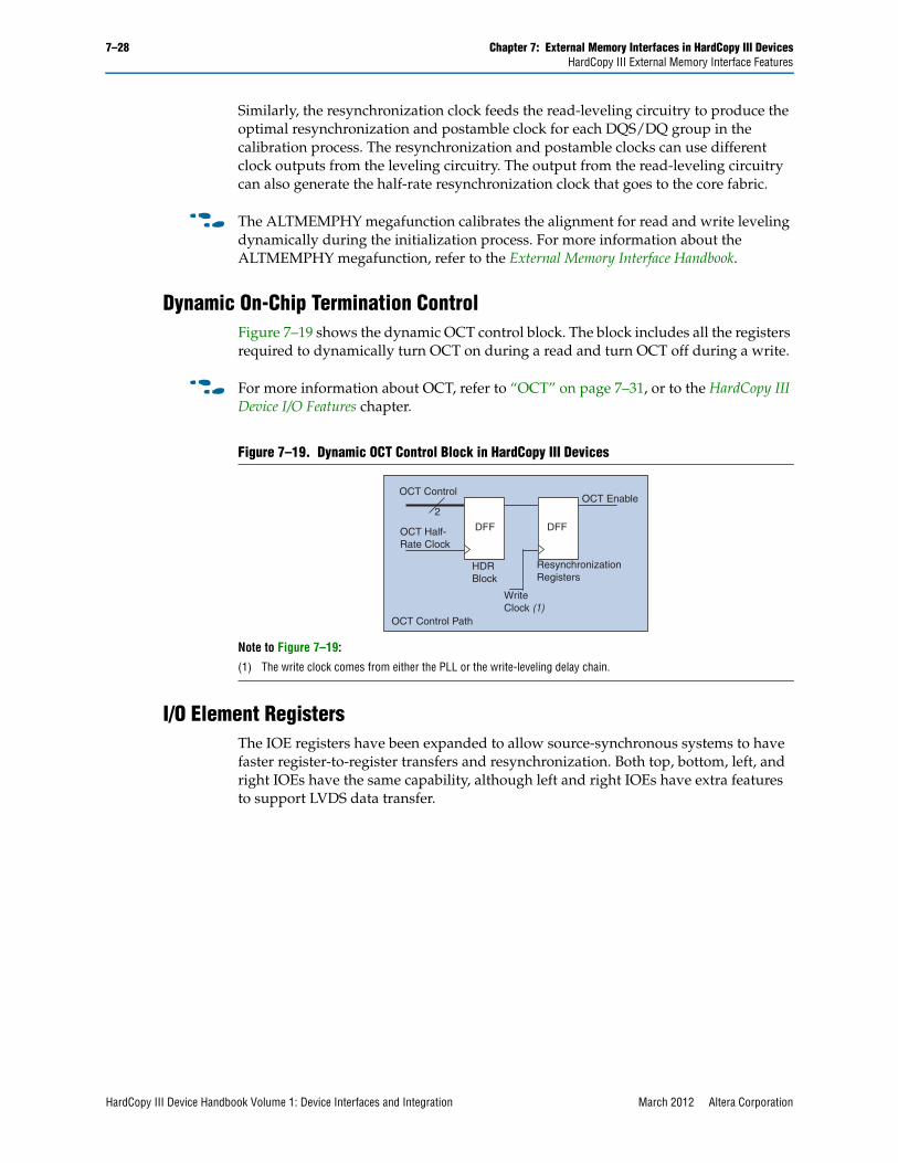
7–28 Chapter 7: External Memory Interfaces in HardCopy III DevicesHardCopy III External Memory Interface Features
HardCopy III Device Handbook Volume 1: Device Interfaces and Integration March 2012 Altera Corporation
Similarly, the resynchronization clock feeds the read-leveling circuitry to produce the optimal resynchronization and postamble clock for each DQS/DQ group in the calibration process. The resynchronization and postamble clocks can use different clock outputs from the leveling circuitry. The output from the read-leveling circuitry can also generate the half-rate resynchronization clock that goes to the core fabric.
f The ALTMEMPHY megafunction calibrates the alignment for read and write leveling dynamically during the initialization process. For more information about the ALTMEMPHY megafunction, refer to the External Memory Interface Handbook.
Dynamic On-Chip Termination ControlFigure 7–19 shows the dynamic OCT control block. The block includes all the registers required to dynamically turn OCT on during a read and turn OCT off during a write.
f For more information about OCT, refer to “OCT” on page 7–31, or to the HardCopy III Device I/O Features chapter.
I/O Element RegistersThe IOE registers have been expanded to allow source-synchronous systems to have faster register-to-register transfers and resynchronization. Both top, bottom, left, and right IOEs have the same capability, although left and right IOEs have extra features to support LVDS data transfer.
Figure 7–19. Dynamic OCT Control Block in HardCopy III Devices
Note to Figure 7–19:
(1) The write clock comes from either the PLL or the write-leveling delay chain.
OCT Control
WriteClock (1)
OCT Enable
Resynchronization Registers
OCT Half-Rate Clock
OCT Control Path
DFFDFF
2
HDRBlock

Chapter 7: External Memory Interfaces in HardCopy III Devices 7–29HardCopy III External Memory Interface Features
March 2012 Altera Corporation HardCopy III Device Handbook Volume 1: Device Interfaces and Integration
Figure 7–20 shows the registers available in the HardCopy III input path. The input path consists of the DDR input registers, resynchronization registers, and HDR block. You can bypass each block of the input path.
There are three registers in the DDR input registers block. Two registers capture data on the positive and negative edges of the clock, while the third register aligns the captured data. You can choose to have the same clock for the positive edge and negative edge registers, or two different clocks (DQS for positive-edge register and CQn for negative-edge register). The third register that aligns the captured data uses the same clock as the positive-edge register.
The resynchronization registers consist of up to three levels of registers to resynchronize the data to the system clock domain. These registers are clocked by the resynchronization clock that is either generated by the PLL or the read-leveling delay chain. The outputs of the resynchronization registers can go straight to the core or to the HDR blocks, which are clocked by the divided-down resynchronization clock.
For more information about the read-leveling delay chain, refer to “Leveling Circuitry” on page 7–26.
Figure 7–20. IOE Input Registers in HardCopy III Devices (Note 1)
Notes to Figure 7–20:
(1) You can bypass each register block in this path.(2) This is the 0-phase resynchronization clock from the read-leveling delay chain.(3) The input clock can be from the DQS logic block (whether the postamble circuitry is bypassed or not) or from a global clock line.(4) This input clock comes from the CQn logic block.(5) This resynchronization clock can come either from the PLL or from the read-leveling delay chain.(6) The I/O clock divider resides adjacent to the DQS logic block. In addition to the PLL and read levelled resync clock, the I/O clock divider can also
be fed by the DQS bus or CQn bus.(7) The half-rate data and clock signals feed into a FIFO in the core.(8) You can change the dataoutbypass signal dynamically after the device enters user mode.
DFF
I
DFF
Input Reg A
Input Reg B
neg_reg_out
I
D Q
D Q
01
DQS (3)
CQn (4)
DQ
Input Reg CI
DFF
D Q
DFF
DFF
D Q
D Q
DFF
D Q
DFF
DFF
D Q
D Q
DFF
D Q
Resynchronization Clock(resync_clk_2x)(5)
Alignment & Synchronization Registers Double Data Rate Input Registers
Half Data Rate Registers
To Core (rdata0) (7)
To Core (rdata1)
(7)
To Core (rdata2) (7)
To Core (rdata3)
(7)
to core (7)
Half-Rate Resynchronization Clock (resync_clk_1x)
0
0
1
1
dataoutbypass(8)
I/O Clock Divider (6)
(2)
DFF
D Q
DFF
D Q
DFF
D Q
DFF
D Q
DFF
D Q
DFF
D Q
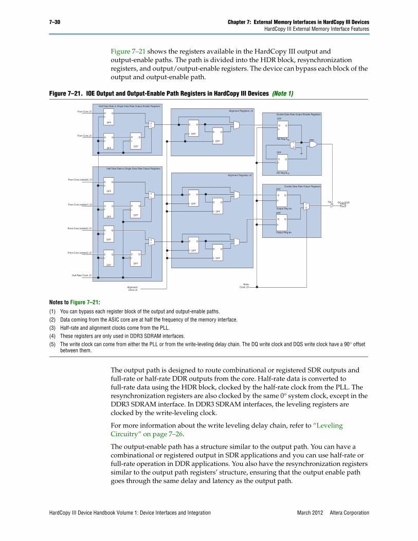
7–30 Chapter 7: External Memory Interfaces in HardCopy III DevicesHardCopy III External Memory Interface Features
HardCopy III Device Handbook Volume 1: Device Interfaces and Integration March 2012 Altera Corporation
Figure 7–21 shows the registers available in the HardCopy III output and output-enable paths. The path is divided into the HDR block, resynchronization registers, and output/output-enable registers. The device can bypass each block of the output and output-enable path.
The output path is designed to route combinational or registered SDR outputs and full-rate or half-rate DDR outputs from the core. Half-rate data is converted to full-rate data using the HDR block, clocked by the half-rate clock from the PLL. The resynchronization registers are also clocked by the same 0° system clock, except in the DDR3 SDRAM interface. In DDR3 SDRAM interfaces, the leveling registers are clocked by the write-leveling clock.
For more information about the write leveling delay chain, refer to “Leveling Circuitry” on page 7–26.
The output-enable path has a structure similar to the output path. You can have a combinational or registered output in SDR applications and you can use half-rate or full-rate operation in DDR applications. You also have the resynchronization registers similar to the output path registers’ structure, ensuring that the output enable path goes through the same delay and latency as the output path.
Figure 7–21. IOE Output and Output-Enable Path Registers in HardCopy III Devices (Note 1)
Notes to Figure 7–21:
(1) You can bypass each register block of the output and output-enable paths.(2) Data coming from the ASIC core are at half the frequency of the memory interface.(3) Half-rate and alignment clocks come from the PLL.(4) These registers are only used in DDR3 SDRAM interfaces.(5) The write clock can come from either the PLL or from the write-leveling delay chain. The DQ write clock and DQS write clock have a 90° offset
between them.
Alignment Registers (4)
DFF
DFF
D Q
D Q
DFF
D Q
DFF
DFF
D Q
D Q
DFF
D Q
Half Data Rate to Single Data Rate Output Registers
DFF
DFF
D Q
D Q
DFF
D Q
Half Data Rate to Single Data Rate Output-Enable Registers
Alignment Registers (4)
AlignmentClock (3)
01
0
1
01
From Core (2)
From Core (2)
From Core (wdata0) (2)
From Core (wdata1) (2)
From Core (wdata2) (2)
From Core (wdata3) (2)
D Q
DFF
D Q
DFF
01
Output Reg Ao
Output Reg Bo
D Q
DFF
D Q
DFF
OR2
TRI
OE Reg BOE
OE Reg AOE
0
1
Double Data Rate Output-Enable Registers
Double Data Rate Output Registers
DQ or DQS
WriteClock (5)
Half-Rate Clock (3)
DFF
D Q
DFF
D Q
DFF
D Q
DFF
D Q
DFF
D QDFF
D Q

Chapter 7: External Memory Interfaces in HardCopy III Devices 7–31HardCopy III External Memory Interface Features
March 2012 Altera Corporation HardCopy III Device Handbook Volume 1: Device Interfaces and Integration
IOE FeaturesThis section describes how OCT, delay chains, output delay, slew rate control, and drive strength setting are useful in memory interfaces.
1 These IOE features are mask programmed and cannot be changed after the silicon is fabricated.
f For more information about the features listed below, refer to the HardCopy III Device I/O Features chapter.
OCTHardCopy III devices feature dynamic calibrated OCT, in which the series termination (OCT RS) is turned on when driving signals and turned off when receiving signals, and the parallel termination (OCT RT) is turned off when driving signals and turned on when receiving signals. This feature complements the DDR3/DDR2 SDRAM on-die termination (ODT), in which the memory termination is turned off when the memory is sending data and turned on when receiving data. You can use OCT for other memory interfaces to improve signal integrity.
1 You cannot use the drive strength and slew rate features when using OCT RS.
To use the dynamic calibrated OCT feature, you must use the RUP and RDN pins to calibrate the OCT calibration block. You can use one OCT calibration block to calibrate one type of termination with the same VCCIO on the entire device. There are up to eight OCT calibration blocks to allow for different types of terminations throughout the device. For more information, refer to “Dynamic On-Chip Termination Control” on page 7–28.
1 You have the option to use the OCT RS feature with or without calibration. However, the OCT RT feature is only available with calibration.
You can also use the RUP and RDN pins as DQ pins, so you cannot use the DQS/DQ groups where the RUP and RDN pins are located if you are planning to use dynamic calibrated OCT. The RUP and RDN pins are located in the first and last ×4 DQS/DQ group on each side of the device.
Use the OCT RT or RS setting for unidirectional read-and-write data and a dynamic OCT setting for bidirectional data signals.
IOE Delay ChainsYou can use the delay chains in the HardCopy III I/O registers as deskewing circuitry. Each pin can have a different input delay from the pin to the input register or a delay from the output register to the output pin to ensure that the bus has the same delay going into or out of the device. This feature helps read and write time margins because it minimizes the uncertainties between signals in the bus.

7–32 Chapter 7: External Memory Interfaces in HardCopy III DevicesHardCopy III External Memory Interface Features
HardCopy III Device Handbook Volume 1: Device Interfaces and Integration March 2012 Altera Corporation
Output Buffer DelayIn addition to allowing for output buffer duty-cycle adjustment, the output buffer delay chain allows you to adjust the delays between the data bits in your output bus to introduce or compensate channel-to-channel skew. Incorporating skew to the output bus can help minimize simultaneous switching events by enabling smaller parts of the bus to switch simultaneously instead of the whole bus. This feature is useful in DDR3 SDRAM interfaces where the memory system clock delay can be much larger than the data and data clock/strobe delay. You can use this delay chain to add delay to the data and data clock/strobe to better match the memory system clock delay.
Slew Rate ControlHardCopy III devices provide four levels of static output slew rate control—0, 1, 2, and 3; Level 0 is the slowest slew rate setting and level 3 is the fastest slew rate setting. The default setting for the HSTL and SSTL I/O standards is 3. A fast slew rate setting allows you to achieve higher I/O performance; a slow slew-rate setting reduces system noise and signal overshoot. This feature is disabled if you use the OCT RS features.
Drive StrengthYou can choose the optimal drive strength required for your interface after performing board simulation. Higher drive strength helps provide a larger voltage swing, which in turn provides bigger eye diagrams with greater timing margin. However, higher drive strengths typically require more power, result in faster slew rates, and add to simultaneous switching noise (SSN). You can use the slew rate control with this feature to minimize SSN with higher drive strengths. This feature is also disabled if you use the OCT RS feature, which is the default drive strength in HardCopy III devices. Use the OCT RT/RS setting for unidirectional read-and-write data and the dynamic OCT setting for bidirectional data signals. You must simulate the system to determine the drive strength required for command, address, and clock signals.
PLLYou can use PLLs to generate the memory interface controller clocks, such as the 0° system clock, the –90° or 270° phase-shifted write clock, the half-rate PHY clock, and the resynchronization clock. You can also use the PLL reconfiguration feature to calibrate the resynchronization phase shift to balance the setup and hold margin. The VCO and counter setting combinations may be limited for high-performance memory interfaces.
Altera recommends enabling the PLL reconfiguration feature and the DLL phase offset feature (DLL reconfiguration) for HardCopy III devices. Because HardCopy III devices are mask programmed, they cannot be changed after the silicon is fabricated. By implementing these two features, you can perform timing adjustments to improve or resolve timing issues after the silicon is fabricated.

Chapter 7: External Memory Interfaces in HardCopy III Devices 7–33Document Revision History
March 2012 Altera Corporation HardCopy III Device Handbook Volume 1: Device Interfaces and Integration
1 PLL reconfiguration is not required for the ALTMEMPHY AFI because it uses auto-calibration. Adding PLL reconfiguration adds very little value and the ALTMEMPHY IP which is generated is not PLL-reconfiguration friendly. Altera strongly recommends implementing PLL reconfiguration for the UniPHY IP.
f For more information about HardCopy III PLLs, refer to the Clock Networks and PLLs in HardCopy III Devices chapter.
Document Revision HistoryTable 7–10 lists the revision history for this chapter.
Table 7–10. Document Revision History
Date Version Changes
March 2012 3.2■ Updated DLLx numbering in Figure 7–1, Figure 7–3, Figure 7–4, Figure 7–5, Figure 7–6,
Figure 7–7, and Figure 7–8.
■ Updated DLLx numbering in Table 7–5, Table 7–6, Table 7–7, and Table 7–8.
January 2011 3.1
■ Updated Figure 7–1.
■ Updated Table 7–2 and Table 7–6.
■ Updated to include UniPhy IP information.
■ Changed the External DDR Memory PHY Interface Megafunction User Guide (ALTMEMPHY) link to the External Memory Interface Handbook link.
■ Minor text edits.
June 2009 3.0
■ Updated Table 7–1, Table 7–2, and Table 7–5.
■ Added Figure Table 7–8.
■ Updated “DLL” on page 7–19.
■ Removed “Conclusion” and “Referenced Documents” sections.
December 2008 2.0 Format changes.
May 2008 1.0 Initial release.

7–34 Chapter 7: External Memory Interfaces in HardCopy III DevicesDocument Revision History
HardCopy III Device Handbook Volume 1: Device Interfaces and Integration March 2012 Altera Corporation
HardCopy III Device Handbook Volume 1: Device Interfaces and IntegrationJanuary 2011
HIII51008-3.2
Subscribe
© 2011 Altera Corporation. All rights reserved. ALTERA, ARRIA, CYCLONE, HARDCOPY, MAX, MEGACORE, NIOS, QUARTUS and STRATIX are Reg. U.S. Pat. & Tm. Off. and/or trademarks of Altera Corporation in the U.S. and other countries. All other trademarks and service marks are the property of their respective holders as described at www.altera.com/common/legal.html. Altera warrants performance of its semiconductor products to current specifications in accordance with Altera’s standard warranty, but reserves the right to make changes to any products and services at any time without notice. Altera assumes no responsibility or liability arising out of the application or use of any information, product, or service described herein except as expressly agreed to in writing by Altera. Altera customers are advised to obtain the latest version of device specifications before relying on any published information and before placing orders for products or services.
8. High-Speed Differential I/O Interfacesand DPA in HardCopy III Devices
The HardCopy® III device family offers up to 1.25-Gbps differential I/O capabilities to support source-synchronous communication protocols such as Utopia, RapidIO®, XSBI, SGMII, SFI, and SPI. HardCopy III and Stratix® III devices have identical circuitry for high-speed differential I/O interfaces and dynamic phase alignment (DPA). HardCopy III high-speed I/Os support the same I/O standards and implementation guidelines as Stratix III devices. You can prototype high-speed interfaces with Stratix III devices and map the design to HardCopy III devices.
1 Because of differences in resource availability, you must set the HardCopy III companion device option in the Quartus® II software to map your Stratix III project to a HardCopy III device.
HardCopy III devices have the same dedicated circuitry as Stratix III devices for high-speed differential I/O support:
■ Differential I/O buffer
■ Transmitter serializer
■ Receiver deserializer
■ Data realignment
■ DPA
■ Synchronizer (FIFO buffer)
■ Analog phase-locked looks (PLLs) located on the left and right sides of the device
For high-speed differential interfaces, HardCopy III devices support the following differential I/O standards:
■ Low voltage differential signaling (LVDS)
■ Mini-LVDS
■ Reduced swing differential signaling (RSDS)
■ Differential HSTL
■ Differential SSTL
You can use HSTL and SSTL I/O standards only for PLL clock inputs and outputs in differential mode.
January 2011HIII51008-3.2

8–2 Chapter 8: High-Speed Differential I/O Interfaces and DPA in HardCopy III DevicesI/O Banks
HardCopy III Device Handbook Volume 1: Device Interfaces and Integration January 2011 Altera Corporation
I/O Banks HardCopy III I/Os are divided into 12 to 20 I/O banks. The dedicated circuitry that supports high-speed differential I/Os is located in the left and right (row) I/O banks of the device. Figure 8–1 shows the different banks and the I/O standards supported by the banks.
Figure 8–1. I/O Banks in HardCopy III Devices (Note 1), (2), (3), (4), (5), (6)
Notes to Figure 8–1:
(1) The 1152- and 1517-pin packages have 20 I/O banks. The 780-pin package has 16 I/O banks. The 484-pin package has 12 I/O banks.(2) Figure 8–1 is a top view of the silicon die that corresponds to a reverse view for flip-chip packages. It is a graphical representation only. For exact
locations, refer to the pin list and Quartus II software.(3) Differential HSTL and SSTL I/Os use two single-ended outputs with the second output programmed as inverted for the transmitter and uses a true
SSTL/HSTL differential input buffer for the receiver.(4) Top and bottom I/O differential HSTL and SSTL inputs use LVDS differential input buffers without on-chip differential termination support.(5) Top and bottom I/O supports LVDS outputs using single-ended buffers and external resistor networks.(6) The PLL blocks are shown for location purposes only and are not considered additional banks. The PLL input and output uses the I/Os in adjacent
banks.
PLL_L1
PLL_L4 PLL_R4
PLL_R1
PLL_L2
PLL_L3
PLL_T2PLL_T1
Ban
k 1A
Bank 8A
Ban
k 1C
Ban
k 2C
Ban
k 2A
Bank 8B Bank 7B Bank 7ABank 7CBank 8C
PLL_B2PLL_B1Bank 3A Bank 3B Bank 4B Bank 4ABank 4CBank 3C
PLL_R2
PLL_R3
Ban
k 6A
Ban
k 6C
Ban
k 5C
Ban
k 5A
I/O banks 8A, 8B & 8C support all single-ended and differential input and output operations
I/O banks 7A, 7B & 7C support all single-ended and differential input and output operations
I/O banks 3A, 3B & 3C support all single-ended and differential input and output operations
I/O banks 4A, 4B & 4C support all single-ended and differential input and output operations
Row I/O banks support LVTTL, LVCMOS, 2.5-V, 1.8V,1.5-V, 1.2-V, SSTL-2 Class I & II, SSTL-18 Class I & II,SSTL-15 Class I, HSTL-18 Class I & II, HSTL-15 Class I,HSTL-12 Class I, LVDS, RSDS, mini-LVDS, differentialSSTL-2 Class I & II, differential SSTL-18 Class I & II,differential SSTL-15 Class I, differential HSTL-18 Class I &II, differential HSTL-15 Class I and differential HSTL-12Class I standards for input and output operations
SSTL-15 class II, HSTL-15 Class II, HSTL-12 Class II,differential SSTL-15 Class II, differential HSTL-15 Class II,and differential HSTL-12 Class II standards are only supportedfor input operations

Chapter 8: High-Speed Differential I/O Interfaces and DPA in HardCopy III Devices 8–3LVDS Channels
January 2011 Altera Corporation HardCopy III Device Handbook Volume 1: Device Interfaces and Integration
LVDS ChannelsHardCopy III devices support LVDS on both row I/O banks and column I/O banks. There are true LVDS input and output buffers on row I/O banks. On column I/O banks, there are true LVDS input buffers but neither true LVDS output buffers nor dedicated high-speed circuitry. However, you can configure all column user I/Os, including I/Os with true LVDS input buffers, as emulated LVDS output buffers. Table 8–1 lists the LVDS channels supported in HardCopy III device row I/O banks.
Table 8–2 lists the LVDS channels supported in HardCopy III device column I/O banks.
Table 8–1. LVDS Channels Supported in HardCopy III Device Left and Right (Row) I/O Banks (Note 1), (2), (3)
HardCopy III Device
484 - Pin FineLine BGA
780 - Pin FineLine BGA
1152-Pin FineLine BGA
1517-Pin FineLine BGA (4)
HC325W 48Rx + 48Tx 48Rx + 48Tx — —
HC325F 48Rx + 48Tx 56Rx + 56Tx — —
HC335L — — 88Rx + 88Tx 88Rx + 88Tx (5)
HC335F — — 88Rx + 88Tx 88Rx + 88Tx (5)
Notes to Table 8–1:
(1) The LVDS channel count does not include dedicated clock input pins.(2) The HardCopy III device family does not offer a 1760-pin package. (3) Rx = true LVDS input buffers with OCT RD, Tx = true LVDS output buffers, and eTx = emulated LVDS output buffers
(either LVDS_E_1R or LVDS_E_3R).(4) The HardCopy III device family does not offer a 1517-pin package for Stratix III EP3SL110 and EP3SL150
prototype devices.(5) Stratix III devices EP3SL340F1517 and EP3SE260F1517 offer 112Rx + 112Tx or 224eTx channels, and thus have
more transceiver channels than HardCopy III devices.
Table 8–2. LVDS Channels Supported in HardCopy III Device Top and Bottom (Column) I/O Banks (Note 1), (2), (3) (Part 1 of 2)
HardCopy III Device 484 - Pin FineLine BGA
780 - Pin FineLine BGA
1152-Pin FineLine BGA
1517-Pin FineLine BGA
HC325W
24Rx + 24eTx
or
48eTx
48Rx + 48eTx
or
96eTx
— —
HC325F
24Rx + 24eTx
or
48eTx
64Rx + 64eTx
or
128eTx
— —
HC335L — —
96Rx + 96eTx
or
192eTx
128Rx + 128eTx
or
256eTx (4)

8–4 Chapter 8: High-Speed Differential I/O Interfaces and DPA in HardCopy III DevicesDifferential Transmitter
HardCopy III Device Handbook Volume 1: Device Interfaces and Integration January 2011 Altera Corporation
1 For more information about high-speed differential I/O interfaces and DPA, refer to “Design Recommendations” on page 8–22 and “Differences Between Stratix III and HardCopy III Devices” on page 8–23.
Differential TransmitterThe HardCopy III transmitter has dedicated circuitry to provide support for LVDS signaling. The dedicated circuitry consists of a differential buffer, a serializer, and a shared analog PLL (left or right PLL). The differential buffer can drive out LVDS, mini-LVDS, and RSDS signaling levels. The serializer takes up to 10 bits-wide parallel data from the FPGA core, clocks it into the load registers, and serializes it using shift registers clocked by the left or right PLL before sending the data to the differential buffer. The MSB of the parallel data is transmitted first.
The load and shift registers are clocked by the load enable (load_en) signal and the diffioclk (clock running at serial data rate) signal generated from PLL_Lx (left PLL) or PLL_Rx (right PLL). You can statically set the serialization factor to ×4, ×6, ×7, ×8, or ×10 by using the Quartus II software. The load enable signal is derived from the serialization factor setting. Figure 8–2 is a block diagram of the HardCopy III transmitter.
HC335F — —
96Rx + 96eTx
or
192eTx
128Rx + 128eTx
or
256eTx (4)
Notes to Table 8–2:
(1) The LVDS channel count does not include dedicated clock input pins.(2) LVDS input buffers at top and bottom I/O banks are true LVDS input buffers. All user I/Os, including I/Os with true
LVDS input buffers, can be configured as emulated LVDS output buffers.(3) Rx = true LVDS input buffers with OCT RD, Tx = true LVDS output buffers, and eTx = emulated LVDS output buffers
(either LVDS_E_1R or LVDS_E_3R).(4) The HardCopy III device family does not offer a 1517-pin package for Stratix III EP3SL110 and EP3SL150 prototype
devices.
Table 8–2. LVDS Channels Supported in HardCopy III Device Top and Bottom (Column) I/O Banks (Note 1), (2), (3) (Part 2 of 2)
HardCopy III Device 484 - Pin FineLine BGA
780 - Pin FineLine BGA
1152-Pin FineLine BGA
1517-Pin FineLine BGA

Chapter 8: High-Speed Differential I/O Interfaces and DPA in HardCopy III Devices 8–5Differential Transmitter
January 2011 Altera Corporation HardCopy III Device Handbook Volume 1: Device Interfaces and Integration
You can configure the HardCopy III transmitter data channel to generate a source synchronous transmitter clock output, allowing you to place the output clock near the data outputs to simplify board layout and reduce clock-to-data skew. Different applications often require specific clock-to-data alignments or specific data rate to clock rate factors. The transmitter can output a clock signal at the same rate as the data. Depending on the serialization factor, the output clock can also be divided by a factor of 2, 4, 8, or 10. You can set the phase of the clock in relation to the data at 0° or 180° (edge or center aligned). The left and right PLLs (PLL_Lx and PLL_Rx) provide additional support for other phase shifts in 45° increments. These settings are made statically in the Quartus II MegaWizard™ Plug-In Manager. Figure 8–3 shows the HardCopy III transmitter in clock output mode.
Figure 8–2. Transmitter for HardCopy III Devices
InternalLogic
Serializer
PLL_Lx / PLL_Rx
diffioclk
load_en
10TX_OUT
Figure 8–3. Transmitter in Clock Output Mode for HardCopy III Devices
Transmitter Circuit
diffioclk
load_en
Txclkout–Txclkout+
Parallel Series
InternalLogic
PLL_Lx / PLL_Rx

8–6 Chapter 8: High-Speed Differential I/O Interfaces and DPA in HardCopy III DevicesDifferential Receiver
HardCopy III Device Handbook Volume 1: Device Interfaces and Integration January 2011 Altera Corporation
You can bypass the HardCopy III serializer to support double data rate (DDR) (×2) and single data rate (SDR) (×1) operations to achieve a serialization factor of 2 and 1, respectively. The I/O element (IOE) contains two data output registers that can each operate in either DDR or SDR mode. The clock source for the registers in the IOE can come from any routing resource, from the left or right PLL (PLL_Lx/PLL_Rx), or from the top or bottom (PLL_Tx/PLL_Bx) PLL. Figure 8–4 shows the serializer bypass path.
Differential Receiver HardCopy III devices have dedicated circuitry for receiving high-speed differential signals. Figure 8–5 shows a HardCopy III receiver block diagram. The receiver has a differential buffer, a shared PLL_Lx/PLL_Rx, DPA, synchronization FIFO buffer, data realignment block, and a deserializer. The differential buffer can receive LVDS, mini-LVDS, and RSDS signal levels, which are statically set in the Quartus II software Assignment Editor. The PLL receives the external source clock input that is transmitted with the data and generates different phases of the same clock. The DPA block chooses one of the clocks from the left or right PLL and aligns the incoming data on each channel.
Figure 8–4. Serializer Bypass for HardCopy III Devices
Txclkout–Txclkout+
IOE
SerializerInternal Logic
IOE Supports SDR, DDR, orNon-Registered Data Path
Not used (connection exists)
Figure 8–5. Receiver Block Diagram for HardCopy III Devices
D Q
8
10–+
data retimed_data
DPA_clk
Eight Phase Clocks
DedicatedReceiverInterface
DPA Bypass Multiplexer
Input data stream
DPA
PLL _Lx / PLL_Rx
diffioclkload_enrx_inclk
Synchronizer
InternalLogic
Regional orGlobal Clock
DataRealignment
Circuitry

Chapter 8: High-Speed Differential I/O Interfaces and DPA in HardCopy III Devices 8–7Receiver Data Realignment Circuit (Bit Slip)
January 2011 Altera Corporation HardCopy III Device Handbook Volume 1: Device Interfaces and Integration
The synchronizer circuit is a 1-bit wide by 6-bit deep FIFO buffer that compensates for any phase difference between the DPA clock and the data realignment block. If necessary, the data realignment circuit inserts a single bit of latency in the serial bit stream to align to the word boundary. The deserializer includes shift registers and parallel load registers and sends a maximum of 10 bits to the internal logic. The data path in the HardCopy III receiver is clocked by either a diffioclk signal or the DPA recovered clock. You can statically set the deserialization factor to 4, 6, 7, 8, or 10 by using the Quartus II software. The left or right PLLs (PLL_Lx/PLL_Rx) generate the load enable signal, which is derived from the deserialization factor setting.
You can bypass the HardCopy III deserializer in the Quartus II MegaWizard Plug-In Manager to support DDR (×2) or SDR (×1) operations. You cannot use the DPA and the data realignment circuit when you bypass the deserializer. The IOE contains two data input registers that can operate in DDR or SDR mode. The clock source for the registers in the IOE can come from any routing resource, from the left or right PLLs, or from the top or bottom PLLs. Figure 8–6 shows the deserializer bypass data path.
Receiver Data Realignment Circuit (Bit Slip)Skew in the transmitted data, along with skew added by the link, causes channel-to-channel skew on the received serial data streams. If the DPA is enabled, the received data is captured with different clock phases on each channel. This may cause the received data to be misaligned from channel to channel. To compensate for this channel-to-channel skew and establish the correct received word boundary at each channel, each receiver channel has a dedicated data realignment circuit that realigns the data by inserting bit latencies into the serial stream.
An optional RX_CHANNEL_DATA_ALIGN port controls the bit insertion of each receiver independently controlled from the internal logic. The data slips one bit for every pulse on RX_CHANNEL_DATA_ALIGN. The following conditions are required for the RX_CHANNEL_DATA_ALIGN signal:
■ The minimum pulse width is one period of the parallel clock in the logic array
■ The minimum low time between pulses is one period of the parallel clock
■ There is no maximum high or low time
■ Valid data is available two parallel clock cycles after the rising edge of RX_CHANNEL_DATA_ALIGN
Figure 8–6. Deserializer Bypass
rx_in IOE
DeserializerDPA
Circuitry
HardCopy Logic Array
IOE Supports SDR, DDR, orNon-Registered Data Path

8–8 Chapter 8: High-Speed Differential I/O Interfaces and DPA in HardCopy III DevicesDynamic Phase Aligner
HardCopy III Device Handbook Volume 1: Device Interfaces and Integration January 2011 Altera Corporation
Figure 8–7 shows the receiver output (rx_out) after one bit slip pulse with the serialization factor set to 4.
The data realignment circuit can have up to 11 bit-times of insertion before a rollover occurs. The bit rollover point can be from 1 to 11 bit-times, independent of the deserialization factor. An optional status port, rx_cda_max, is available to the FPGA from each channel to indicate when the preset rollover point is reached.
Dynamic Phase Aligner The dynamic phase aligner (DPA) block takes in high-speed serial data from the differential input buffer and selects one of the eight phase clocks from the left or right PLL to sample the data. The DPA chooses a phase closest to the phase of the serial data. The maximum phase offset between the received data and the selected phase is 1/8 unit interval (UI), which is the maximum quantization error of the DPA. The eight phases of the clock are equally divided, giving a 45° resolution. Figure 8–8 shows the possible phase relationships between the DPA clocks and the incoming serial data.
The DPA block continuously monitors the phase of the incoming serial data and selects a new clock phase if required. You can prevent the DPA from selecting a new clock phase by asserting the optional rx_dpll_hold port, which is available for each channel.
Figure 8–7. Data Realignment Timing
rx_in
rx_outclock
rx_channel_data_align
rx_out
inclk
3
3210 321x xx21 0321
2 1 0 3 2 1 0 3 2 1 0
Figure 8–8. DPA Clock Phase to Serial Data Timing Relationship
45˚
90˚
135˚
180˚
225˚
270˚
315˚
0.125Tvco
Tvco
0˚
rx_in D0 D1 D2 D3 D4 Dn

Chapter 8: High-Speed Differential I/O Interfaces and DPA in HardCopy III Devices 8–9Soft-CDR Mode
January 2011 Altera Corporation HardCopy III Device Handbook Volume 1: Device Interfaces and Integration
The DPA block requires a training pattern and a training sequence of at least 256 repetitions. The training pattern is not fixed, so you can use any training pattern with at least one transition on each channel. An optional output port (rx_dpa_locked) is available to the internal logic to indicate when the DPA block has settled on the closest phase to the incoming data phase. The DPA block de-asserts rx_dpa_locked depending on the option selected in the Quartus II MegaWizard Plug-In Manager, when either a new phase is selected, or when the DPA has moved two phases in the same direction. The rx_dpa_locked signal is synchronized to the DPA clock domain and should be considered as the initial indicator for the lock condition. Use data checkers to validate the data integrity.
An independent reset port (rx_reset) is available to reset the DPA circuitry. The DPA circuitry must be retrained after reset.
Soft-CDR ModeThe HardCopy III LVDS channel offers soft-CDR mode to support the Gigabit Ethernet/SGMII protocols. Clock-data recovery (CDR) is required to extract the clock out of the clock-embedded data to support SGMII. In HardCopy III devices, the CDR circuit is implemented in HCells.
In soft-CDR mode, the DPA circuitry selects an optimal DPA clock phase to sample the data and carry on the bit-slip operation and deserialization. The selected DPA clock is also divided down by the deserialization factor and then forwarded to the PLD core along with the de-serialized data. The LVDS block has an output called divclkout for the forwarded clock signal. This signal is put on the periphery clock network. In HardCopy III devices, you can use every LVDS channel in soft-CDR mode and can drive the core using the periphery network. Figure 8–9 shows the path enabled in soft-CDR mode.
Figure 8–9. Soft-CDR Mode Data and Clock Path (Note 1)
Note to Figure 8–9:
(1) The synchronizer FIFO is bypassed in soft-CDR mode. The reference clock frequency must be suitable for the PLL to generate a clock that matches the data rate of the interface. The DPA circuitry can track parts per million (PPM) differences between the reference clock and the data stream.
Deserializer Bit SlipDPA
PLL
ReTimedData LVDS Data
DPACLOCKTREE
RefClock
Divide Downand
Clock Forwarding
Data to Core
CLK_BS_DES
DPA CLK
PCLK
10
core

8–10 Chapter 8: High-Speed Differential I/O Interfaces and DPA in HardCopy III DevicesSynchronizer
HardCopy III Device Handbook Volume 1: Device Interfaces and Integration January 2011 Altera Corporation
Synchronizer The synchronizer is a 1-bit × 6-bit deep FIFO buffer that compensates for the phase difference between the recovered clock from the DPA circuit and the diffioclk that clocks the rest of the logic in the receiver. The synchronizer can only compensate for phase differences, not frequency differences between the data and the receiver’s inclk.
An optional port (rx_fifo_reset) is available to the internal logic to reset the synchronizer. The synchronizer is automatically reset when the DPA first locks to the incoming data. Altera recommends using rx_fifo_reset to reset the synchronizer when the DPA signals a loss-of-lock condition beyond the initial locking condition.
Pre-Emphasis and Output Differential Voltage HardCopy III LVDS transmitters support four pre-emphasis and four output differential voltage (VOD) settings. Pre-emphasis increases the amplitude of the high frequency component of the output signal and helps compensate for the frequency dependent attenuation along the transmission line. Figure 8–10 shows an LVDS output with pre-emphasis. The overshoot is produced by pre-emphasis. This overshoot must not be included in the VOD voltage. The definition of VOD is also shown in Figure 8–10.
Pre-emphasis is an important feature for high-speed transmission. Without pre-emphasis, the output current is limited by the VOD setting and the output impedance of the driver. At high frequency, the slew rate might not be fast enough to reach the full VOD before the next edge, producing a pattern dependent jitter.
With pre-emphasis, the output current is boosted momentarily during switching to increase the output slew rate. The overshoot introduced by the extra current happens only during switching and does not ring, unlike the overshoot caused by signal reflection. The amount of pre-emphasis required depends on the attenuation of the high-frequency component along the transmission line.
Figure 8–10. Output Differential Voltage
OUT
OUT
VOD
Overshoot
Undershoot

Chapter 8: High-Speed Differential I/O Interfaces and DPA in HardCopy III Devices 8–11Differential I/O Termination
January 2011 Altera Corporation HardCopy III Device Handbook Volume 1: Device Interfaces and Integration
You can adjust pre-emphasis in HardCopy III devices to create the right amount of overshoot at different transmission conditions. There are four settings for pre-emphasis: zero, low, medium, and high. The default setting is low. For a particular design, you can use simulation with an LVDS buffer and transmission line to determine the best pre-emphasis setting. You can also fix the VOD to any of the four settings: low, medium low, medium high, and high. The default setting is medium low.
1 A re-compile is required for each new setting.
Differential I/O TerminationHardCopy III devices provide a 100-, on-chip differential termination option on each differential receiver channel for LVDS standards. On-chip termination (OCT) saves board space by eliminating the need to add external resistors on the board. You can enable OCT in the Quartus II Assignment Editor.
On-chip differential termination is supported on all row I/O pins and serial/deserializer (SERDES) block clock pins: clk[0,2,9,11]. It is not supported for column I/O pins, high speed clock pins clk[1,3,8,10], or the corner PLL clock inputs. Figure 8–11 shows device OCT.
Left and Right PLLs (PLL_Lx and PLL_Rx)HardCopy III devices contain a maximum of eight left or right PLLs with up to four PLLs located on the left side (PLL_L1, PLL_L2, PLL_L3, and PLL_L4) and four on the right side (PLL_R1, PLL_R2, PLL_R3, and PLL_R4) of the device. The left PLLs can support high-speed differential I/O banks on the left side; the right PLLs can support banks only on the right side of the device. The high-speed differential I/O receiver and transmitter channels use these left and right PLLs to generate the parallel clocks (rx_outclock and tx_outclock) and high-speed clocks (diffioclk). Figure 8–1 on page 8–2 show the locations of the left/right PLLs for HardCopy III devices. The PLL VCO operates at the clock frequency of the data rate. Each left or right PLL offers a single serial data rate support, but up to two separate serialization or deserialization factors (from the C0 and C1 of left or right PLL clock outputs), or both. Clock switchover and dynamic left and right PLL reconfiguration are available in high-speed differential I/O support mode.
Figure 8–11. On-Chip Differential OCT
LVDSTransmitter
HardCopy III DifferentialReceiver with On-Chip
100 Ω Termination
RD
Z0 = 50 Ω
Z0 = 50 Ω

8–12 Chapter 8: High-Speed Differential I/O Interfaces and DPA in HardCopy III DevicesClocking
HardCopy III Device Handbook Volume 1: Device Interfaces and Integration January 2011 Altera Corporation
Figure 8–12 shows a simplified diagram of the major components of a HardCopy III PLL.
Clocking The left and right PLLs feed into the differential transmitter and receiver channels through the LVDS and DPA clock networks. Figure 8–13 and Figure 8–14 show the corner and center PLL clock in HardCopy III devices. Each left or right I/O bank consists of one LVDS clock network, for a total of four clock trees on the device. The center left and right PLLs can drive the LVDS clock network, therefore, clocking the transmitter and receiver channels above and below them. The corner left and right PLLs can drive the adjacent row-I/O banks only. For example, corner PLL_L1 can drive the LVDS clock network only in I/O bank 1A and bank 1C. Therefore, with corner PLLs, each LVDS clock network can be driven by three PLLs: two center PLLs and one corner PLL. For HardCopy III devices without a corner PLL, each clock tree
Figure 8–12. PLL for HardCopy III Devices
ClockSwitchover
Block
inclk0
inclk1
Clock inputsfrom pins
GCLK/RCLK
Cascade inputfrom adjacent PLL
pfdena
clkswitchclkbad0clkbad1activeclock
PFD
LockCircuit
locked
÷n CP LF VCO ÷284
FBINdiffioclk networkGCLK/RCLK network
no compensation modeZDB, External feedback modesLVDS Compensation modeSource Synchronous, normal modes
÷C0
÷C1
÷C2
÷C3
÷Cn
÷m
PLL O
utp
ut M
ux
Casade outputto adjacent PLL
GCLKs
RCLKs
External clockoutputs
diffioclk fromLeft/Right PLLs
load_en fromLeft/Right PLLs
FBOUT
Externalmemoryinterface DLL
88
To DPA block onLeft/Right PLLs
/2, /4
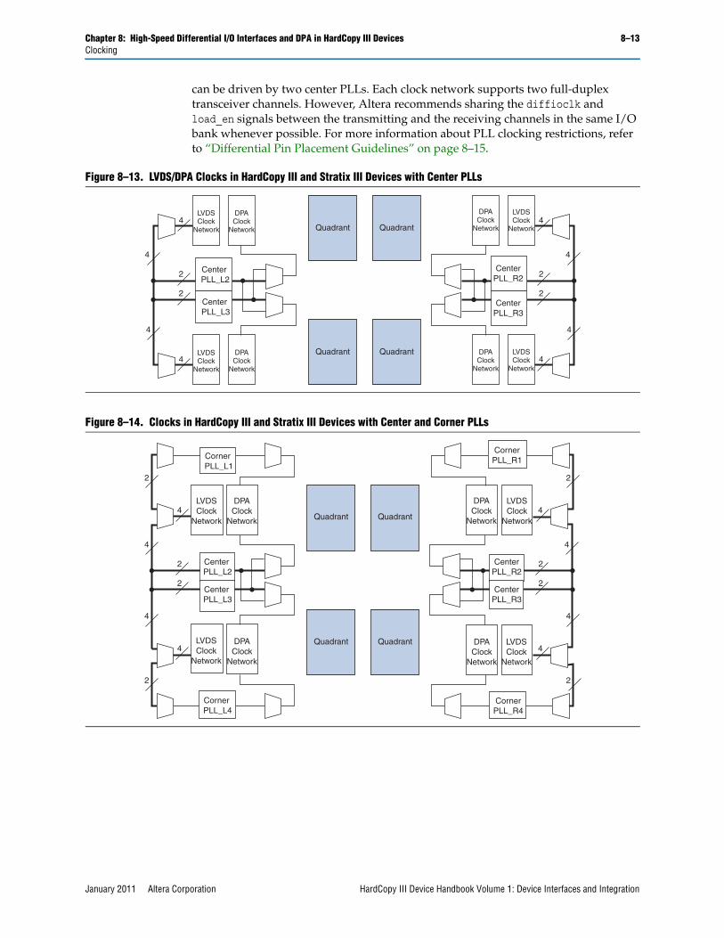
Chapter 8: High-Speed Differential I/O Interfaces and DPA in HardCopy III Devices 8–13Clocking
January 2011 Altera Corporation HardCopy III Device Handbook Volume 1: Device Interfaces and Integration
can be driven by two center PLLs. Each clock network supports two full-duplex transceiver channels. However, Altera recommends sharing the diffioclk and load_en signals between the transmitting and the receiving channels in the same I/O bank whenever possible. For more information about PLL clocking restrictions, refer to “Differential Pin Placement Guidelines” on page 8–15.
Figure 8–13. LVDS/DPA Clocks in HardCopy III and Stratix III Devices with Center PLLs
Figure 8–14. Clocks in HardCopy III and Stratix III Devices with Center and Corner PLLs
4
2
2
2
2
4
4
4
4
4
4
4
Quadrant Quadrant
Quadrant Quadrant
LVDSClock
Network
Center PLL_L2
Center PLL_L3
DPAClock
Network
LVDSClock
Network
DPAClock
Network
LVDSClock
Network
CenterPLL_R2
CenterPLL_R3
DPAClock
Network
LVDSClock
Network
DPAClock
Network
4
2
2
2
2
4
Quadrant Quadrant
Quadrant Quadrant
LVDSClock
Network
Center PLL_L2
Center PLL_L3
LVDSClock
Network
DPAClock
Network
2
4
2
4
4
4
2
4
2
4
LVDSClock
Network
CenterPLL_R2
CenterPLL_R3
DPAClock
Network
LVDSClock
Network
DPAClock
Network
Corner PLL_L1
Corner PLL_L4
DPAClock
Network
CornerPLL_R1
CornerPLL_R4

8–14 Chapter 8: High-Speed Differential I/O Interfaces and DPA in HardCopy III DevicesHigh-Speed Differential I/O Interfaces and DPA in HardCopy III Devices Differential Data Orientation
HardCopy III Device Handbook Volume 1: Device Interfaces and Integration January 2011 Altera Corporation
High-Speed Differential I/O Interfaces and DPA in HardCopy III Devices Differential Data Orientation
There is a set relationship between an external clock and the incoming data. For operation at 1 Gbps with a SERDES factor of 10, the external clock is multiplied by 10, and phase-alignment is set in the PLL to coincide with the sampling window of each data bit. The data is sampled on the falling edge of the multiplied clock. Figure 8–15 shows the data bit orientation of the ×10 mode.
Data synchronization is necessary for successful data transmission at high frequencies. Figure 8–16 shows the data bit orientation for a channel operation. This figure is based on the following:
■ SERDES factor equals clock multiplication factor
■ Edge alignment is selected for phase alignment
■ Implemented in hard SERDES
Figure 8–15. Bit Orientation in Quartus II Software Differential I/O Bit Position
9 8 7 6 5 4 3 2 1 0
10 LVDS BitsMSB LSB
inclock/outclock
data in
Figure 8–16. Bit-Order and Word Boundary for One Differential Channel (Note 1)
Note to Figure 8–16:
(1) These are only functional waveforms and are not intended to convey timing information.
Previous Cycle7 6 5 4 3 2 1 0
MSB LSB
tx_outclock
tx_out X X X X X X X X X X X X X X X XCurrent Cycle Next Cycle
Transmitter ChannelOperation (x8 Mode)
X X X X X X X X
rx_inclock
rx_in 7 6 5 4 3 2 1 0 X X X X X X X X X X X X X X X X
Receiver ChannelOperation (x8 Mode)
rx_inclock
rx_in
rx_outclock
rx_out [3..0]
X X X X X XX X X X X X
Receiver ChannelOperation (x4 Mode)
3 2 1 0
X X X X X X X X X X X X 3210
rx_outclock
rx_out [7..0] X X X X X X X X X X X X X X X X X X X X 7 6 5 4 3 2 1 0 X X X X
Chapter 8: High-Speed Differential I/O Interfaces and DPA in HardCopy III Devices 8–15Differential Pin Placement Guidelines
January 2011 Altera Corporation HardCopy III Device Handbook Volume 1: Device Interfaces and Integration
For other serialization factors, use the Quartus II software tools and find the bit position within the word. The bit positions after deserialization are listed in Table 8–3.
Table 8–3 shows the conventions for differential bit naming for eight differential channels. The MSB and LSB positions increase with the number of channels used in a system.
Differential Pin Placement Guidelines To ensure proper high-speed operation, differential pin placement guidelines have been established. Also, the Quartus II compiler automatically verifies these guidelines and issues an error message if they are not met.
Because DPA usage adds some constraints on the placement of high-speed differential channels, this section is divided into pin placement guidelines with and without DPA usage.
f If you want to place both single-ended and differential I/Os in the same row or column I/O bank, refer to the HardCopy III Device I/O Features chapter.
Guidelines for DPA-Enabled Differential ChannelsHardCopy III devices have differential receivers and transmitters in I/O banks on the left and right sides of the device. Each receiver has a dedicated DPA circuit to align the phase of the clock to the data phase of its associated channel. When you use DPA-enabled channels in differential banks, you must adhere to the guidelines listed in the following sections.
Using Corner and Center Left/Right PLLsIf a differential bank is being driven by two left or right PLLs, and the corner left or right PLL is driving one group and the center left or right PLL is driving another group, there must be at least one row of separation between the two groups of DPA-enabled channels (refer to Figure 8–17). The two groups can operate at independent frequencies.
Table 8–3. LVDS Channels Supported in HardCopy III Device Left and Right (Row) I/O Banks
Receiver Channel NumberInternal 8-Bit Parallel Data
MSB Position LSB Position
1 7 0
2 15 8
3 23 16
4 31 24
5 39 32
6 47 40
7 55 48
8 63 56

8–16 Chapter 8: High-Speed Differential I/O Interfaces and DPA in HardCopy III DevicesDifferential Pin Placement Guidelines
HardCopy III Device Handbook Volume 1: Device Interfaces and Integration January 2011 Altera Corporation
No separation is necessary if a single left or right PLL is driving DPA-enabled channels as well as DPA-disabled channels.
You can use center left or right PLLs to drive DPA-enabled channels simultaneously, as long as they drive these channels in their adjacent banks only, as shown in Figure 8–18.
Figure 8–17. Corner and Center Left/Right PLLs Driving DPA-Enabled Differential I/Os in the Same Bank Using Both Center Left/Right PLLs
Diff I/O
CornerLeft/Right PLL
CenterLeft/Right PLL
One UnusedChannel for Buffer
Channels driven byCenter Left/Right PLL
Channels driven byCorner Left/Right PLL
ReferenceCLK
ReferenceCLK
DPA-enabledDiff I/O
DPA-enabledDiff I/O
DPA-enabledDiff I/O
DPA-enabledDiff I/O
DPA-enabledDiff I/O
DPA-enabledDiff I/O
DPA-enabledDiff I/O
DPA-enabledDiff I/O
DPA-enabledDiff I/O

Chapter 8: High-Speed Differential I/O Interfaces and DPA in HardCopy III Devices 8–17Differential Pin Placement Guidelines
January 2011 Altera Corporation HardCopy III Device Handbook Volume 1: Device Interfaces and Integration
If one of the center left or right PLLs drives the top and bottom banks, you cannot use the other center left or right PLL to drive differential channels, as shown in Figure 8–18.
Figure 8–18. Center Left/Right PLLs Driving DPA-Enabled Differential I/Os
CornerLeft/Right PLL
CornerLeft/Right PLL
CenterLeft/Right PLL
CenterLeft/Right PLL
Maximum 26 channelsdriven by the upper centerleft/right PLL
Maximum 26 channelsdriven by the centerleft/right PLL
Maximum 26 channelsdriven by the centerleft/right PLL
Maximum 26 channelsdriven by the upper centerleft/right PLL
ReferenceCLK
ReferenceCLK
ReferenceCLK
ReferenceCLK
DPA-enabledDiff I/O
DPA-enabledDiff I/O
DPA-enabledDiff I/O
DPA-enabledDiff I/O
DPA-enabledDiff I/O
DPA-enabledDiff I/O
DPA-enabledDiff I/O
DPA-enabledDiff I/O
CornerLeft/Right PLL
CornerLeft/Right PLL
CenterLeft/Right PLL
CenterLeft/Right PLL
One UnusedChannel for Buffer
Maximum 26 channelsdriven by the upper centerleft/right PLL
Maximum 26 channelsdriven by the upper centerleft/right PLL
ReferenceCLK
ReferenceCLK
ReferenceCLK
ReferenceCLK
DPA-enabledDiff I/O
DPA-enabledDiff I/O
DPA-enabledDiff I/O
DPA-enabledDiff I/O
DPA-enabledDiff I/O
DPA-enabledDiff I/O
DPA-enabledDiff I/O
DPA-enabledDiff I/O
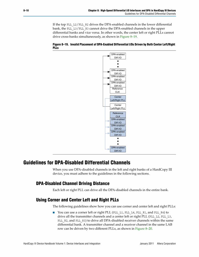
8–18 Chapter 8: High-Speed Differential I/O Interfaces and DPA in HardCopy III DevicesGuidelines for DPA-Disabled Differential Channels
HardCopy III Device Handbook Volume 1: Device Interfaces and Integration January 2011 Altera Corporation
If the top PLL_L2/PLL_R2 drives the DPA-enabled channels in the lower differential bank, the PLL_L3/PLL_R3 cannot drive the DPA-enabled channels in the upper differential banks and vice versa. In other words, the center left or right PLLs cannot drive cross-banks simultaneously, as shown in Figure 8–19.
Guidelines for DPA-Disabled Differential ChannelsWhen you use DPA-disabled channels in the left and right banks of a HardCopy III device, you must adhere to the guidelines in the following sections.
DPA-Disabled Channel Driving DistanceEach left or right PLL can drive all the DPA-disabled channels in the entire bank.
Using Corner and Center Left and Right PLLsThe following guidelines show how you can use corner and center left and right PLLs:
■ You can use a corner left or right PLL (PLL_L1, PLL_L4, PLL_R1, and PLL_R4) to drive all the transmitter channels and a center left or right PLL (PLL_L2, PLL_L3, PLL_R2, and PLL_R3) to drive all DPA-disabled receiver channels within the same differential bank. A transmitter channel and a receiver channel in the same LAB row can be driven by two different PLLs, as shown in Figure 8–20.
Figure 8–19. Invalid Placement of DPA-Enabled Differential I/Os Driven by Both Center Left/Right PLLs
CenterLeft/Right PLL
CenterLeft/Right PLL
ReferenceCLK
ReferenceCLK
DPA-enabledDiff I/O
DPA-enabledDiff I/O
DPA-enabledDiff I/O
DPA-enabledDiff I/O
DPA-enabledDiff I/O
DPA-enabledDiff I/O
DPA-enabledDiff I/O
DPA-enabledDiff I/O
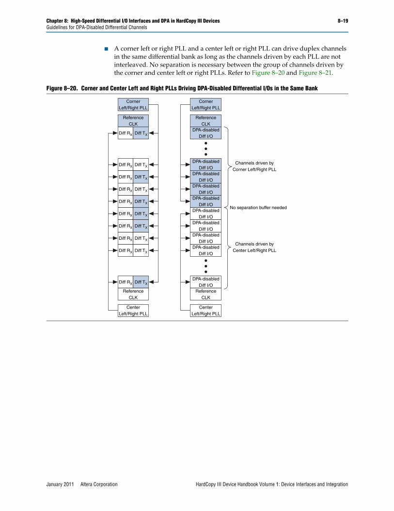
Chapter 8: High-Speed Differential I/O Interfaces and DPA in HardCopy III Devices 8–19Guidelines for DPA-Disabled Differential Channels
January 2011 Altera Corporation HardCopy III Device Handbook Volume 1: Device Interfaces and Integration
■ A corner left or right PLL and a center left or right PLL can drive duplex channels in the same differential bank as long as the channels driven by each PLL are not interleaved. No separation is necessary between the group of channels driven by the corner and center left or right PLLs. Refer to Figure 8–20 and Figure 8–21.
Figure 8–20. Corner and Center Left and Right PLLs Driving DPA-Disabled Differential I/Os in the Same Bank
No separation buffer needed
Channels driven byCenter Left/Right PLL
Channels driven byCorner Left/Right PLL
CornerLeft/Right PLL
Diff RX
Diff RX
Diff RX
Diff RX
Diff RX
Diff RX
Diff RX
Diff RX
Diff RX
Diff TX
Diff TX
Diff TX
Diff TX
Diff TX
Diff TX
Diff TX
Diff TX
Diff TX
Diff TXDiff RX
CornerLeft/Right PLL
CenterLeft/Right PLL
CenterLeft/Right PLL
ReferenceCLK
ReferenceCLK
ReferenceCLK
ReferenceCLK
DPA-disabledDiff I/O
DPA-disabledDiff I/O
DPA-disabledDiff I/O
DPA-disabledDiff I/O
DPA-disabledDiff I/O
DPA-disabledDiff I/O
DPA-disabledDiff I/O
DPA-disabledDiff I/O
DPA-disabledDiff I/O
DPA-disabledDiff I/O
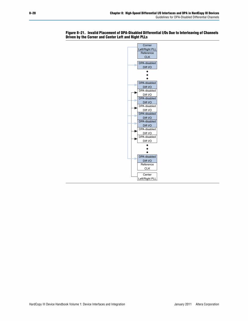
8–20 Chapter 8: High-Speed Differential I/O Interfaces and DPA in HardCopy III DevicesGuidelines for DPA-Disabled Differential Channels
HardCopy III Device Handbook Volume 1: Device Interfaces and Integration January 2011 Altera Corporation
Figure 8–21. Invalid Placement of DPA-Disabled Differential I/Os Due to Interleaving of Channels Driven by the Corner and Center Left and Right PLLs
-
CenterLeft/Right PLL
ReferenceCLK
ReferenceCLK
DPA-disabledDiff I/O
DPA-disabledDiff I/O
DPA-disabledDiff I/O
DPA-disabledDiff I/O
DPA-disabledDiff I/O
DPA-disabledDiff I/O
DPA-disabledDiff I/O
DPA-disabledDiff I/O
DPA-disabledDiff I/O
DPA-disabledDiff I/O
CornerLeft/Right PLL

Chapter 8: High-Speed Differential I/O Interfaces and DPA in HardCopy III Devices 8–21Guidelines for DPA-Disabled Differential Channels
January 2011 Altera Corporation HardCopy III Device Handbook Volume 1: Device Interfaces and Integration
Using Both Center Left and Right PLLsYou can use both center left and right PLLs simultaneously to drive DPA-disabled channels on upper and lower differential banks, as shown in Figure 8–22. Unlike DPA-enabled channels, the center left and right PLLs can drive cross-banks. For example, the upper center left or right PLL can drive the lower differential bank while the lower center left or right PLL is driving the upper differential bank and vice versa, as shown in Figure 8–23.
Figure 8–22. Both Center Left and Right PLLs Simultaneously Driving DPA-Disabled Upper and Lower Bank Channels
LVDS PLL
LVDS PLL
DPA-disabledI/O
DPA-disabledI/O
DPA-disabledI/O
DPA-disabledI/O
DPA-disabledI/O
DPA-disabledI/O
DPA-disabledI/O
DPA-disabledI/O
DPA-disabledI/O
DPA-disabledI/O
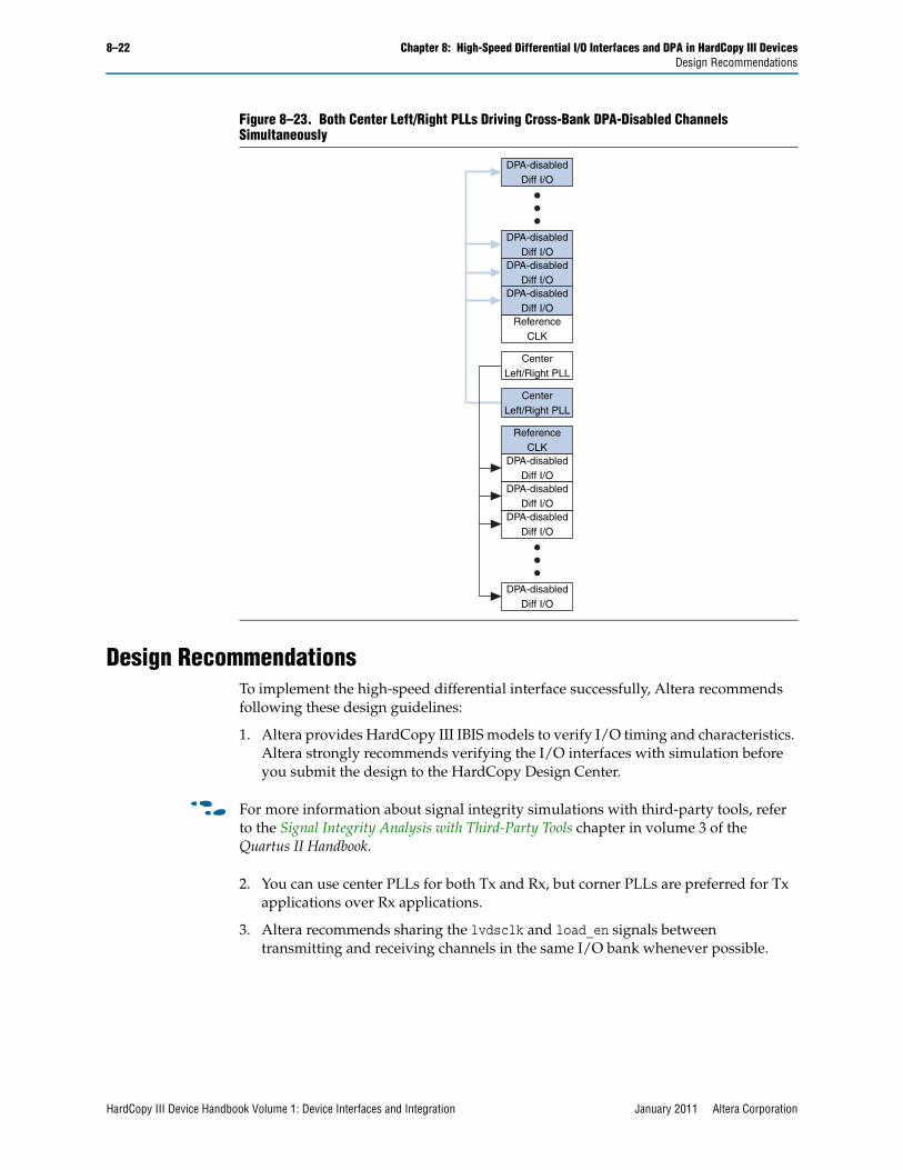
8–22 Chapter 8: High-Speed Differential I/O Interfaces and DPA in HardCopy III DevicesDesign Recommendations
HardCopy III Device Handbook Volume 1: Device Interfaces and Integration January 2011 Altera Corporation
Design RecommendationsTo implement the high-speed differential interface successfully, Altera recommends following these design guidelines:
1. Altera provides HardCopy III IBIS models to verify I/O timing and characteristics. Altera strongly recommends verifying the I/O interfaces with simulation before you submit the design to the HardCopy Design Center.
f For more information about signal integrity simulations with third-party tools, refer to the Signal Integrity Analysis with Third-Party Tools chapter in volume 3 of the Quartus II Handbook.
2. You can use center PLLs for both Tx and Rx, but corner PLLs are preferred for Tx applications over Rx applications.
3. Altera recommends sharing the lvdsclk and load_en signals between transmitting and receiving channels in the same I/O bank whenever possible.
Figure 8–23. Both Center Left/Right PLLs Driving Cross-Bank DPA-Disabled Channels Simultaneously
ReferenceCLK
DPA-disabledDiff I/O
DPA-disabledDiff I/O
DPA-disabledDiff I/O
CenterLeft/Right PLL
ReferenceCLK
DPA-disabledDiff I/O
DPA-disabledDiff I/O
DPA-disabledDiff I/O
DPA-disabledDiff I/O
DPA-disabledDiff I/O
CenterLeft/Right PLL

Chapter 8: High-Speed Differential I/O Interfaces and DPA in HardCopy III Devices 8–23Differences Between Stratix III and HardCopy III Devices
January 2011 Altera Corporation HardCopy III Device Handbook Volume 1: Device Interfaces and Integration
Differences Between Stratix III and HardCopy III DevicesThe HardCopy III device family supports full high-speed differential I/O and DPA mapping from the Stratix III family. Both families are designed with identical dedicated circuitry and thus support the same I/O standard, implementation guidelines, and performance. Table 8–4 shows the LVDS channels supported in Stratix III and HardCopy III devices.
Document Revision HistoryTable 8–5 lists the revision history for this chapter.
Table 8–4. LVDS Channels Supported in Stratix III and HardCopy III Devices (Note 1), (2)
HardCopy III Device
Package (3) LVDS Channels Stratix III Devices Package LVDS Channels
HC325WF484
48Rx + 48Tx
EP3SL150F780
56Rx + 56TxHC325F EP3SE110
HC325WF780
EP3SL200H780
HC325F 56Rx + 56Tx EP3SE260
HC335L
F1152 88Rx + 88Tx
EP3SL150
F115288Rx + 88Tx
EP3SL200
HC335F
EP3SE110
EP3SE260
EP3SL340 H1152
HC335L
F1517 88Rx + 88Tx
EP3SL200
F1517 112Rx + 112TxHC335F
EP3SL340
EP3SE260
Notes to Table 8–4:
(1) The HardCopy III family does not offer a 1760-pin package.(2) LVDS channels supported in HardCopy III and Stratix III devices left and right (row) I/O banks.(3) There is no socket-replacement to the F484-package HardCopy from the F780-package FPGA.
Table 8–5. Document Revision History
Date Version Changes
January 2011 3.2
■ Removed the note before Table 8–1.
■ Updated Table 8–1, Table 8–2, and Table 8–4.
■ Updated the “Pre-Emphasis and Output Differential Voltage” section.
■ Minor text edits.
January 2010 3.1■ Updated Table 8–1 and Table 8–3.
■ Minor text edits.
June 2009 3.0 Updated tables for device part number updates.
December 2008 2.0 Made minor editorial changes.
May 2008 1.0 Initial release.

8–24 Chapter 8: High-Speed Differential I/O Interfaces and DPA in HardCopy III DevicesDocument Revision History
HardCopy III Device Handbook Volume 1: Device Interfaces and Integration January 2011 Altera Corporation

March 2012 Altera Corporation HardCopy III Device Handbook Volume 1: Device Interfaces and Integration
Section III. Hot Socketing and Testing
This section includes the following chapters:
■ Chapter 9, Hot Socketing and Power-On Reset in HardCopy III Devices
■ Chapter 10, IEEE 1149.1 (JTAG) Boundary Scan Testing in HardCopy III Devices
Revision HistoryRefer to each chapter for its own specific revision history. For information on when each chapter was updated, refer to the Chapter Revision Dates section, which appears in the full handbook.

III–2 Section III: Hot Socketing and Testing
HardCopy III Device Handbook Volume 1: Device Interfaces and Integration March 2012 Altera Corporation

HardCopy III Device Handbook Volume 1: Device Interfaces and IntegrationJanuary 2011
HIII51009-2.0
Subscribe
© 2011 Altera Corporation. All rights reserved. ALTERA, ARRIA, CYCLONE, HARDCOPY, MAX, MEGACORE, NIOS, QUARTUS and STRATIX are Reg. U.S. Pat. & Tm. Off. and/or trademarks of Altera Corporation in the U.S. and other countries. All other trademarks and service marks are the property of their respective holders as described at www.altera.com/common/legal.html. Altera warrants performance of its semiconductor products to current specifications in accordance with Altera’s standard warranty, but reserves the right to make changes to any products and services at any time without notice. Altera assumes no responsibility or liability arising out of the application or use of any information, product, or service described herein except as expressly agreed to in writing by Altera. Altera customers are advised to obtain the latest version of device specifications before relying on any published information and before placing orders for products or services.
9. Hot Socketing and Power-On Reset inHardCopy III Devices
This chapter contains information about hot-socketing specifications, power-on reset (POR) requirements, and their implementation in HardCopy® III devices.
HardCopy III devices offer hot socketing, which is also known as hot plug-in or hot swap, and power sequencing support without the use of any external devices. You can insert or remove a HardCopy III device or a board in a system during system operation without causing undesirable effects to the running system bus or the board that was inserted into the system.
The hot-socketing feature also removes some of the difficulty when you use HardCopy III devices or PCBs that contain a mixture of 3.0-, 2.5-, 1.8-, 1.5-, and 1.2-V devices. With the HardCopy III hot-socketing feature, you no longer need to ensure a proper power-up sequence for each device on the board.
The HardCopy III hot-socketing feature provides:
■ Board or device insertion and removal without external components or board manipulation
■ Support for any power-up sequence
■ Non-intrusive I/O buffers to system buses during hot insertion
This chapter also discusses hot-socketing specification, its implementation, and the POR circuitry in HardCopy III devices. The POR circuitry keeps the devices in the reset state until the power supplies are within operating range.
HardCopy III Hot-Socketing SpecificationsHardCopy III devices are hot-socketing compliant without the need for any external components or special design requirements. Hot-socketing support in HardCopy III devices has the following advantages:
■ You can drive the device before power-up without damaging it.
■ I/O pins remain tri-stated during power-up. The device does not drive out before or during power-up and does not affect other buses in operation.
■ You can insert or remove a HardCopy III device from a powered-up system board without damaging or interfering with normal system and board operation.
Devices Can Be Driven Before Power-Up You can drive signals into I/O pins, dedicated input pins, and dedicated clock pins of HardCopy III devices before or during power-up or power-down without damaging the device. HardCopy III devices support power-up or power-down of all power supplies in any sequence to simplify system level design.
January 2011HIII51009-2.0HIV51009-1.1

9–2 Chapter 9: Hot Socketing and Power-On Reset in HardCopy III DevicesHot-Socketing Feature Implementation in HardCopy III Devices
HardCopy III Device Handbook Volume 1: Device Interfaces and Integration January 2011 Altera Corporation
1 HardCopy III ASICs power up to user mode instantly, while Stratix III devices require configuration after power up. If you design a board where a HardCopy III device will replace the Stratix III device, check that all the important signals in your design are ready before the HardCopy III device enters usermode. For example: clocks, resets, and control signals. Otherwise, your system’s operation may be erratic until the proper reset and initialization of your design is performed.
f For more information about the HardCopy III power up behavior, refer to the Matching Stratix III Power and Configuration Requirements with HardCopy III Devices chapter in volume 2 of the HardCopy III Device Handbook.
I/O Pins Remain Tri-Stated During Power-Up A device that does not support hot socketing may interrupt system operation or cause contention by driving out before or during power-up. In a hot-socketing situation, the HardCopy III device’s output buffers are turned off during system power-up or power-down. Also, the HardCopy III device does not drive out until the device is in user mode and working within recommended operating conditions.
Insertion or Removal of a HardCopy III Device from a Powered-Up System Devices that do not support hot socketing can short power supplies when powered up through the device signal pins. This irregular power-up can damage both the driving and driven devices and can disrupt card power-up.
A HardCopy III device may be inserted into (or removed from) a powered-up system board without damaging or interfering with system board operation. You can power-up or power-down all power supplies in any sequence, as long as they are all ramped up to full rail before the HardCopy III device starts to communicate with other devices on the board. This requirement is discussed in “Power-On Reset Circuitry” on page 9–4. HardCopy III devices are immune to latch-up when performing hot socketing.
f For more information about the hot-socketing specification, refer to the DC and Switching Characteristics of HardCopy III Devices chapter in volume 2 of the HardCopy III Handbook.
Hot-Socketing Feature Implementation in HardCopy III Devices The hot-socketing feature turns off the output buffer during power-up and power-down of the VCC, VCCIO, VCCPGM, or VCCPD power supplies. Each I/O pin has the circuitry shown in Figure 9–1.
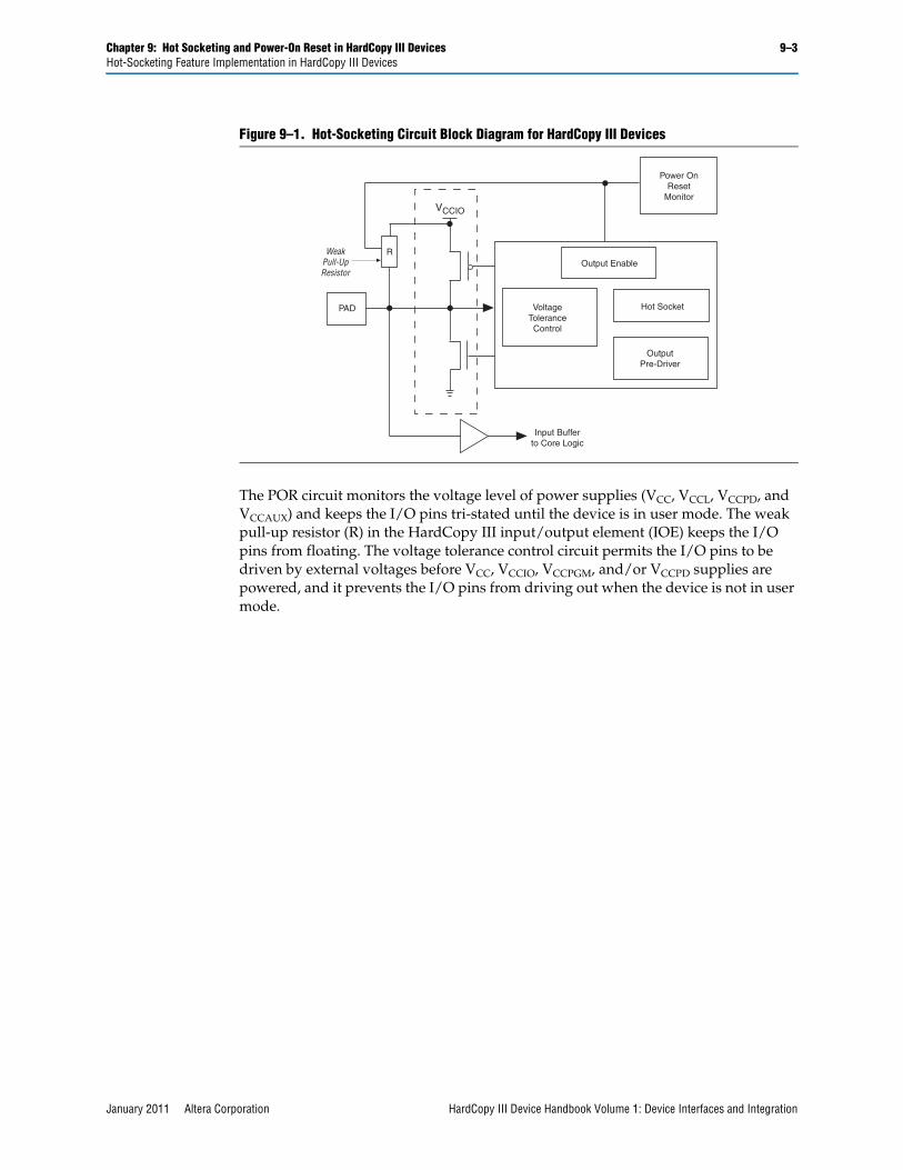
Chapter 9: Hot Socketing and Power-On Reset in HardCopy III Devices 9–3Hot-Socketing Feature Implementation in HardCopy III Devices
January 2011 Altera Corporation HardCopy III Device Handbook Volume 1: Device Interfaces and Integration
The POR circuit monitors the voltage level of power supplies (VCC, VCCL, VCCPD, and VCCAUX) and keeps the I/O pins tri-stated until the device is in user mode. The weak pull-up resistor (R) in the HardCopy III input/output element (IOE) keeps the I/O pins from floating. The voltage tolerance control circuit permits the I/O pins to be driven by external voltages before VCC, VCCIO, VCCPGM, and/or VCCPD supplies are powered, and it prevents the I/O pins from driving out when the device is not in user mode.
Figure 9–1. Hot-Socketing Circuit Block Diagram for HardCopy III Devices
VCCIO
PAD
R
VoltageToleranceControl
Output Enable
Hot Socket
OutputPre-Driver
Power OnReset
Monitor
WeakPull-UpResistor
Input Bufferto Core Logic
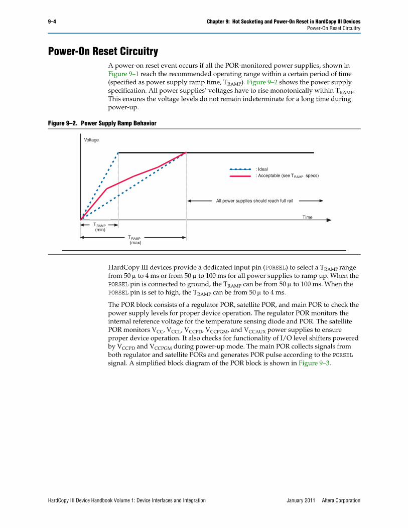
9–4 Chapter 9: Hot Socketing and Power-On Reset in HardCopy III DevicesPower-On Reset Circuitry
HardCopy III Device Handbook Volume 1: Device Interfaces and Integration January 2011 Altera Corporation
Power-On Reset Circuitry A power-on reset event occurs if all the POR-monitored power supplies, shown in Figure 9–1 reach the recommended operating range within a certain period of time (specified as power supply ramp time, TRAMP). Figure 9–2 shows the power supply specification. All power supplies’ voltages have to rise monotonically within TRAMP. This ensures the voltage levels do not remain indeterminate for a long time during power-up.
HardCopy III devices provide a dedicated input pin (PORSEL) to select a TRAMP range from 50 to 4 ms or from 50 to 100 ms for all power supplies to ramp up. When the PORSEL pin is connected to ground, the TRAMP can be from 50 to 100 ms. When the PORSEL pin is set to high, the TRAMP can be from 50 to 4 ms.
The POR block consists of a regulator POR, satellite POR, and main POR to check the power supply levels for proper device operation. The regulator POR monitors the internal reference voltage for the temperature sensing diode and POR. The satellite POR monitors VCC, VCCL, VCCPD, VCCPGM, and VCCAUX power supplies to ensure proper device operation. It also checks for functionality of I/O level shifters powered by VCCPD and VCCPGM during power-up mode. The main POR collects signals from both regulator and satellite PORs and generates POR pulse according to the PORSEL signal. A simplified block diagram of the POR block is shown in Figure 9–3.
Figure 9–2. Power Supply Ramp Behavior
: Ideal: Acceptable (see TRAMP specs)
RAMPT
RAMPT
All power supplies should reach full rail
Voltage
(min)
(max)
Time
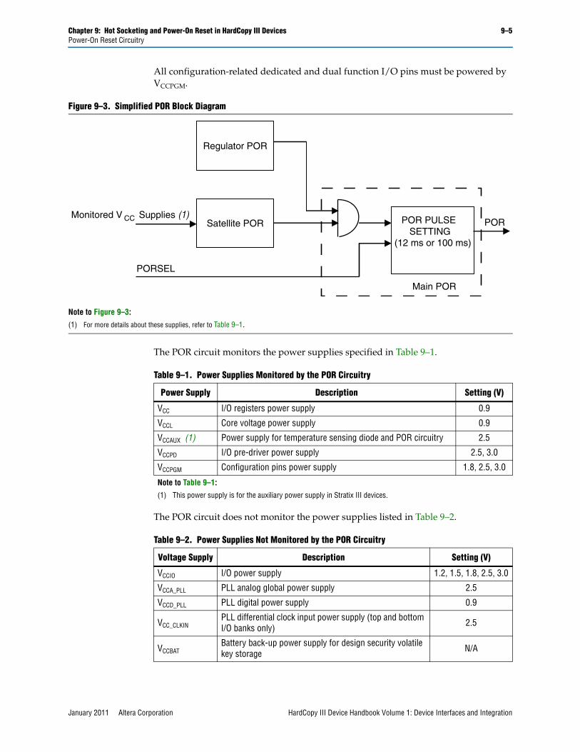
Chapter 9: Hot Socketing and Power-On Reset in HardCopy III Devices 9–5Power-On Reset Circuitry
January 2011 Altera Corporation HardCopy III Device Handbook Volume 1: Device Interfaces and Integration
All configuration-related dedicated and dual function I/O pins must be powered by VCCPGM.
The POR circuit monitors the power supplies specified in Table 9–1.
The POR circuit does not monitor the power supplies listed in Table 9–2.
Figure 9–3. Simplified POR Block Diagram
Note to Figure 9–3:
(1) For more details about these supplies, refer to Table 9–1.
Regulator POR
Satellite POR POR PULSE SETTING
(12 ms or 100 ms)
PORSEL
PORMonitored V Supplies (1)
Main POR
CC
Table 9–1. Power Supplies Monitored by the POR Circuitry
Power Supply Description Setting (V)
VCC I/O registers power supply 0.9
VCCL Core voltage power supply 0.9
VCCAUX (1) Power supply for temperature sensing diode and POR circuitry 2.5
VCCPD I/O pre-driver power supply 2.5, 3.0
VCCPGM Configuration pins power supply 1.8, 2.5, 3.0
Note to Table 9–1:
(1) This power supply is for the auxiliary power supply in Stratix III devices.
Table 9–2. Power Supplies Not Monitored by the POR Circuitry
Voltage Supply Description Setting (V)
VCCIO I/O power supply 1.2, 1.5, 1.8, 2.5, 3.0
VCCA_PLL PLL analog global power supply 2.5
VCCD_PLL PLL digital power supply 0.9
VCC_CLKIN PLL differential clock input power supply (top and bottom I/O banks only) 2.5
VCCBAT Battery back-up power supply for design security volatile key storage N/A

9–6 Chapter 9: Hot Socketing and Power-On Reset in HardCopy III DevicesConclusion
HardCopy III Device Handbook Volume 1: Device Interfaces and Integration January 2011 Altera Corporation
The POR signal pulse width is selectable using the PORSEL input pin. When PORSEL is set to low, the POR signal pulse width is set to 100 ms minimum. When the PORSEL is set to high, the POR signal pulse width is set to minimum. The POR specification is designed to ensure that all circuits in the HardCopy III device are at certain known states during power up.
1 Because not all power supplies are monitored by POR, ensure that the power supplies are fully ramped up before the device starts to communicate with other devices on the system.
Regardless of the voltage level of these power supplies, a HardCopy III device continues to enter user-mode. One difference between Stratix III and HardCopy III devices is that Stratix III devices allow more time for power supplies to ramp up during the configuration phase, before the device enters user mode. HardCopy III devices, however, can enter user mode and release CONF_DONE within 12 ms or 100 ms. Therefore, you should always verify the voltage level of the power supply system before the HardCopy III device starts to run.
f For more information about the POR specification, refer to the DC and Switching Characteristics of HardCopy III Devices chapter in volume 2 of the HardCopy III Handbook.
ConclusionHardCopy III devices are hot-socketing compliant and allow successful device power-up without the need for any power sequencing. The POR circuitry keeps the devices in the reset state until the power supply voltage levels are within operating range.
Document Revision HistoryTable 9–3 shows the revision history for this chapter.
Table 9–3. Document Revision History
Date Version Changes Made
January 2011 2.1■ Updated PORSEL and POR signal pulse information.
■ Updated “Devices Can Be Driven Before Power-Up” on page 9–1.
December 2008 2.0
■ Updated “Power-On Reset Circuitry” on page 9–4.
■ Updated Table 9-1.
■ Updated Figure 9-1.
■ Updated Figure 9-3.
■ Made minor editorial changes.
May 2008 1.0 Initial release.

HardCopy III Device Handbook Volume 1: Device Interfaces and IntegrationJanuary 2011
HIII51010-3.1
Subscribe
© 2011 Altera Corporation. All rights reserved. ALTERA, ARRIA, CYCLONE, HARDCOPY, MAX, MEGACORE, NIOS, QUARTUS and STRATIX are Reg. U.S. Pat. & Tm. Off. and/or trademarks of Altera Corporation in the U.S. and other countries. All other trademarks and service marks are the property of their respective holders as described at www.altera.com/common/legal.html. Altera warrants performance of its semiconductor products to current specifications in accordance with Altera’s standard warranty, but reserves the right to make changes to any products and services at any time without notice. Altera assumes no responsibility or liability arising out of the application or use of any information, product, or service described herein except as expressly agreed to in writing by Altera. Altera customers are advised to obtain the latest version of device specifications before relying on any published information and before placing orders for products or services.
10. IEEE 1149.1 (JTAG) Boundary ScanTesting in HardCopy III Devices
All HardCopy® III ASICs provide Joint Test Action Group (JTAG) boundary-scan test (BST) circuitry that complies with the IEEE Std. 1149.1 specification. The BST architecture offers the capability to efficiently test components on PCBs with tight lead spacing. Pin connections can be tested without using physical test probes, and functional data can be captured while a device is in normal operation. Boundary-scan cells in a device can force signals onto pins, or capture data from pin or core logic signals. Forced test data is serially shifted into the boundary-scan cells. Captured data is serially shifted out and externally compared to expected results.
A device using the JTAG interface uses four required pins: TDI, TDO, TMS, and TCK, and one optional pin, TRST. The TCK pin has an internal weak pull-down resistor, and the TDI, TMS, and TRST pins have internal weak pull-up resistors. The TDO output pin and all the JTAG input pins are powered by the 2.5-V/3.0-V VCCPD supply of I/O bank 1A.
f For more information about the BST architecture and JTAG instructions supported in Stratix III devices, refer to the IEEE 1149.1 (JTAG) Boundary-Scan Testing in Stratix III Devices chapter in volume 1 of the Stratix III Device Handbook.
f For more information about the JTAG pin description, refer to the IEEE 1149.1 (JTAG) Boundary-Scan Testing in Stratix III Devices chapter in volume 1 of the Stratix III Device Handbook.
1 HardCopy III devices only support a maximum I/O voltage of 3.0 V. Consider this when designing your Stratix® III FPGA prototypes and your board so you can successfully map the HardCopy III device.
JTAG InstructionsTable 10–1 shows the JTAG instructions supported in HardCopy III devices for boundary-scan testing (BST). These 10-bit instructions are also supported in Stratix III devices. However, HardCopy III devices do not support the Stratix III JTAG instructions used for in-circuit reconfiguration (ICR), because HardCopy III devices do not require configuration.
January 2011HIII51010-3.1

10–2 Chapter 10: IEEE 1149.1 (JTAG) Boundary Scan Testing in HardCopy III DevicesJTAG Instructions
HardCopy III Device Handbook Volume 1: Device Interfaces and Integration January 2011 Altera Corporation
f For more information about the BST architecture and JTAG instructions supported in Stratix III devices, refer to the IEEE 1149.1 (JTAG) Boundary-Scan Testing in Stratix III Devices chapter in volume 1 of the Stratix III Device Handbook.
1 Similar to Stratix III devices, HardCopy III devices support the SignalTap® II Embedded Logic Analyzer, which monitors design operation over a period of time through the JTAG interface. The SignalTap II Embedded Logic Analyzer is a useful feature during the device prototyping phase, but should be removed if not required after you map the design to a HardCopy III device. HardCopy III devices are mask programmed, and the SignalTap II logic cannot be removed after the HardCopy III device is fabricated.
Table 10–1. HardCopy III JTAG Instructions
JTAG Instruction Instruction Code Description
SAMPLE/PRELOAD 00 0000 0101Allows a snapshot of signals at the device pins to be captured and examined during normal device operation, and permits an initial data pattern to be output at the device pins.
EXTEST (1) 00 0000 1111Allows the external circuitry and board-level interconnects to be tested by forcing a test pattern at the output pins and capturing test results at the input pins.
BYPASS 11 1111 1111Places the 1-bit bypass register between the TDI and TDO pins, which allows the BST data to pass synchronously through selected devices to adjacent devices during normal device operation.
USERCODE 00 0000 0111Loads the 32-bit user code into the device identification register and places the register between the TDI and TDO pins, allowing the user code to be serially shifted out of TDO.
IDCODE 00 0000 0110Loads the 32-bit ID code into the device identification register and places the register between the TDI and TDO pins, allowing the ID code to be serially shifted out of TDO.
HIGHZ (1) 00 0000 1011
Places the 1-bit bypass register between the TDI and TDO pins, which allows the BST data to pass synchronously through selected devices to adjacent devices during normal device operation while tri-stating all of the I/O pins.
CLAMP (1) 00 0000 1010
Places the 1-bit bypass register between the TDI and TDO pins, which allows the BST data to pass synchronously through selected devices to adjacent devices during normal device operation while holding I/O pins to a state defined by the data in the boundary-scan register.
Note to Table 10–1:
(1) The bus hold and weak pull-up resistor features override the high-impedance state of HIGHZ, CLAMP, and EXTEST.

Chapter 10: IEEE 1149.1 (JTAG) Boundary Scan Testing in HardCopy III Devices 10–3Boundary-Scan Register
January 2011 Altera Corporation HardCopy III Device Handbook Volume 1: Device Interfaces and Integration
IDCODE and USERCODEThe IDCODE instruction gives you the ability to shift out a 32-bit identification (ID) code from HardCopy III devices. ID codes are different in Stratix III devices and unique for each HardCopy III device. The ID code can be used to determine the correct device during BST. When the IDCODE instruction is issued, the ID code is loaded into a 32-bit device identification register for shifting out. Table 10–2 shows the ID codes for the HardCopy III devices.
You can use the USERCODE instruction to shift out a 32-bit user code, which can also be used to uniquely identify the device. Unlike Stratix III devices, the user code in HardCopy III devices is mask programmed and cannot be changed after the silicon is fabricated. If the designer does not select a user code, the user code is mask programmed to the default values. When the USERCODE instruction is issued, the 32-bit user code is loaded into the same 32-bit device identification register used for the IDCODE instruction. The user code can then be serially shifted out.
Boundary-Scan RegisterThe boundary-scan register length for HardCopy III devices differs from Stratix III devices. The length also varies for each HardCopy III device depending on the device density and available I/O pin count. Table 10–3 lists the boundary-scan register length for HardCopy III devices.
Boundary-Scan Testing on HardCopy III DevicesThe boundary-scan description language (BSDL), a subset of VHDL, provides a syntax that allows you to describe the features of an IEEE Std. 1149.1 BST-capable device that can be tested.
1 There are two versions of the BSDL Customizer tool that you can use. The pre-configuration version generates a BSDL file for use before the device enters user mode, and the post-configuration version generates a BSDL file for use after the device enters user mode.
Table 10–2. 32-Bit HardCopy III Device IDCODE (Note 1), (2)
DeviceIDCODE (32 Bits)
Version (4 Bits) Part Number (16 Bits) Manufacturer Identity (11 Bits) LSB (1 Bit)
HC325 0000 0010 0010 0010 0101 000 0110 1110 1
HC335 0000 0010 0010 0011 0101 000 0110 1110 1
Notes to Table 10–2:
(1) The most significant bit (MSB) is on the left.(2) The least significant bit (LSB) of IDCODE is always 1.
Table 10–3. HardCopy III Boundary-Scan Register Length
Device Boundary-Scan Register Length
HC325 1524
HC335 2670

10–4 Chapter 10: IEEE 1149.1 (JTAG) Boundary Scan Testing in HardCopy III DevicesJTAG Timing
HardCopy III Device Handbook Volume 1: Device Interfaces and Integration January 2011 Altera Corporation
BSDL files for IEEE Std. 1149.1-compliant HardCopy III devices can also be generated using the Quartus software version 8.1 or later. Visit the Altera website at www.altera.com for the procedure to generate the BSDL files using the Quartus II software.
f For more information about BSDL files for IEEE Std. 1149.1-compliant HardCopy III devices and the BSDL Customizer script, visit the Altera website at www.altera.com.
JTAG TimingFigure 10–1 shows the JTAG timing waveforms for the HardCopy III devices.
f For JTAG timing parameters and values, refer to the DC and Switching Characteristics of HardCopy III Devices chapter in volume 3 of the HardCopy III Device Handbook.
Document Revision HistoryTable 10–4 shows the revision history for this document.
Figure 10–1. JTAG Timing Waveforms for HardCopy III Devices
TDO
TCK
tJPZX tJPCO
tJPH
tJPXZ
tJCP
tJPSU tJCL tJCH
TDI
TMS
Table 10–4. Document Revision History
Date Version Changes
January 2011 3.1 Updated for Quartus II software 10.1.
June 2009 3.0 ■ Updated Table 10–2 and Table 10–3.
December 2008 2.0■ Updated Table 10–3.
■ Minor editorial changes made.
May 2008 1.0 Initial release.

March 2012 Altera Corporation HardCopy III Device Handbook Volume 1: Device Interfaces and Integration
Section IV. Power and ThermalManagement
This section includes the following chapter:
■ Chapter 11, Power Management in HardCopy III Devices
Revision HistoryRefer to each chapter for its own specific revision history. For information on when each chapter was updated, refer to the Chapter Revision Dates section, which appears in the full handbook.

IV–2 Section IV: Power and Thermal Management
HardCopy III Device Handbook Volume 1: Device Interfaces and Integration March 2012 Altera Corporation

HardCopy III Device Handbook Volume 1: Device Interfaces and IntegrationJanuary 2011
HIII51011-3.2
Subscribe
© 2011 Altera Corporation. All rights reserved. ALTERA, ARRIA, CYCLONE, HARDCOPY, MAX, MEGACORE, NIOS, QUARTUS and STRATIX are Reg. U.S. Pat. & Tm. Off. and/or trademarks of Altera Corporation in the U.S. and other countries. All other trademarks and service marks are the property of their respective holders as described at www.altera.com/common/legal.html. Altera warrants performance of its semiconductor products to current specifications in accordance with Altera’s standard warranty, but reserves the right to make changes to any products and services at any time without notice. Altera assumes no responsibility or liability arising out of the application or use of any information, product, or service described herein except as expressly agreed to in writing by Altera. Altera customers are advised to obtain the latest version of device specifications before relying on any published information and before placing orders for products or services.
11. Power Management in HardCopy IIIDevices
Altera® HardCopy® III devices and Stratix® III devices are manufactured with different process technologies. The HardCopy III devices are based on a 0.9-V, 40 nm process, while Stratix III devices are manufactured with a 1.1-V, 65 nm process. Because of the unique voltage requirements of each device family, you must design your board's power supply to support both Stratix III and HardCopy III devices. In addition, you must take into consideration that both device families consume power differently. This chapter describes the power supply requirements and power management solutions for HardCopy III devices.
This chapter contains the following sections:
■ “HardCopy III Device External Power Supply Requirements”
■ “Supporting HardCopy III and Stratix III Power Supplies” on page 11–2
■ “HardCopy III Power Optimization” on page 11–3
■ “Temperature Sensing Diode (TSD)” on page 11–4
■ “External Pin Connections” on page 11–4
HardCopy III Device External Power Supply RequirementsThis section describes the different external power supplies you need to power HardCopy III devices. Table 11–1 lists the external power supply pins for HardCopy III E devices. You can supply some of the power supply pins with the same external power supply, provided their supply voltage levels are the same.
f For possible values of each power supply, refer to the DC and Switching Characteristics of HardCopy III Devices chapter.
Table 11–1. HardCopy III Power Supply Requirements (Part 1 of 2)
Power Supply Pin
Stratix III Voltage Value (V)
HardCopy III Voltage Value (V) Description
VCCL (1) 0.9 / 1.1 (Selectable Core Voltage) 0.9 Core voltage power supply
VCC 1.1 0.9 I/O registers power supply
VCCIO 1.2 / 1.5 / 1.8 / 2.5 / 3.0 / 3.3
1.2 / 1.5 / 1.8 / 2.5 / 3.0 (2) I/O power supply
VCCPGM 1.8 / 2.5 / 3.0 / 3.3 1.8 / 2.5 / 3.0 Configuration pins power supply
VCCPD (3) 2.5 / 3.0 /3.3 2.5 / 3.0 I/O pre-driver power supply
VCCA_PLL 2.5 2.5 PLL analog global power to the PLL regulator
VCCD_PLL 1.1 0.9 PLL digital global power supply
VCC_CLKIN2.5 2.5 Differential clock input pins power supply (top and
bottom I/O banks only)
January 2011HIII51011-3.2

11–2 Chapter 11: Power Management in HardCopy III DevicesSupporting HardCopy III and Stratix III Power Supplies
HardCopy III Device Handbook Volume 1: Device Interfaces and Integration January 2011 Altera Corporation
3.3-V I/O Standard SupportThe maximum I/O power supply voltage of Stratix III and HardCopy III devices is different due to unique process technologies. Stratix III devices support up to 3.3-V I/O voltage and HardCopy III devices support up to 3.0-V I/O voltage because of the long term reliability of 40 nm process technology. Therefore, HardCopy III devices do not support 3.3-V I/O standards such as 3.3-V LVTTL or 3.3-V LVCMOS.
f For more information about 3.3-V I/O standards, refer to the HardCopy III Device I/O Features chapter.
Similarly, Stratix III devices that are prototyped for HardCopy III devices are limited in selection to 3.0-V power supplies. Even so, HardCopy III 3.0-V I/Os can still properly interface with 3.3-V external ports with little loss in noise margin, given similar input and output voltage electrical characteristics.
Supporting HardCopy III and Stratix III Power SuppliesThe three core power rails in both Stratix III and HardCopy III devices are: VCC, VCCL, and VCCD_PLL. For Stratix III devices, the VCC and VCCD_PLL core power rails can be powered by a 1.1-V source, and the VCCL rail is powered by either 0.9-V or 1.1-V source. HardCopy III power rails, on the other hand, are all powered by a 0.9-V source.
Table 11–2 shows the summary of core voltage requirements for these two devices.
VCCBAT2.5 — (6) Battery back-up power supply for design security volatile
key register
VCCPT2.5 2.5 Power supply for the temperature sensing diode and
power-on-reset (POR) (4)
VREF VREF (5) VREF Power supply for the voltage-referenced I/O standards
GND GND GND Ground
Notes to Table 11–1:
(1) VCCL and VCC can be driven with the same voltage regulator when VCCL = VCC as required by the Stratix III device.(2) HardCopy III devices do not support 3.3-V I/O standards.(3) VCCPD can be either 2.5 V or 3.0 V. For a 3.0-V I/O standard, VCCPD = 3.0 V. For 2.5 V I/O standard and below, VCCPD = 2.5 V.(4) In Stratix III devices, this power supply is also used for programmable power technology.(5) There is one VREF pin per I/O bank. You can use an external power supply or a resistor divider network to supply this voltage.(6) This power pin can be disconnected or remain connected on the board.
Table 11–1. HardCopy III Power Supply Requirements (Part 2 of 2)
Power Supply Pin
Stratix III Voltage Value (V)
HardCopy III Voltage Value (V) Description
Table 11–2. Core Voltage Requirements for Stratix III and HardCopy III Devices
Symbol Parameter Stratix III Devices HardCopy III Devices Unit
VCC I/O registers power supply 1.1 0.9 V
VCCL Core voltage supply 0.9/1.1 (Selectable Core Voltage) 0.9 V
VCCD_PLL PLL digital power supply 1.1 0.9 V
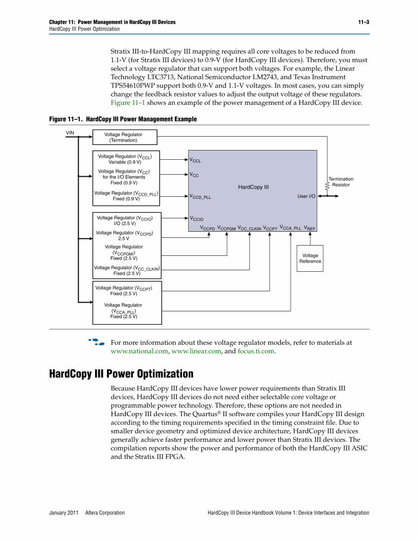
Chapter 11: Power Management in HardCopy III Devices 11–3HardCopy III Power Optimization
January 2011 Altera Corporation HardCopy III Device Handbook Volume 1: Device Interfaces and Integration
Stratix III-to-HardCopy III mapping requires all core voltages to be reduced from 1.1-V (for Stratix III devices) to 0.9-V (for HardCopy III devices). Therefore, you must select a voltage regulator that can support both voltages. For example, the Linear Technology LTC3713, National Semiconductor LM2743, and Texas Instrument TPS54610PWP support both 0.9-V and 1.1-V voltages. In most cases, you can simply change the feedback resistor values to adjust the output voltage of these regulators. Figure 11–1 shows an example of the power management of a HardCopy III device.
f For more information about these voltage regulator models, refer to materials at www.national.com, www.linear.com, and focus.ti.com.
HardCopy III Power OptimizationBecause HardCopy III devices have lower power requirements than Stratix III devices, HardCopy III devices do not need either selectable core voltage or programmable power technology. Therefore, these options are not needed in HardCopy III devices. The Quartus® II software compiles your HardCopy III design according to the timing requirements specified in the timing constraint file. Due to smaller device geometry and optimized device architecture, HardCopy III devices generally achieve faster performance and lower power than Stratix III devices. The compilation reports show the power and performance of both the HardCopy III ASIC and the Stratix III FPGA.
Figure 11–1. HardCopy III Power Management Example
VIN
Voltage Regulator (VCCL)Variable (0.9 V)
Voltage Regulator (VCCD_PLL)Fixed (0.9 V)
Voltage Regulator (VCC_CLKIN)Fixed (2.5 V)
Voltage Regulator (VCC)for the I/O Elements
Fixed (0.9 V)
Voltage Regulator (VCCIO)I/O (2.5 V)
Voltage Regulator (VCCPD)2.5 V
Voltage Regulator(VCCPGM/)
Fixed (2.5 V)
VCCL
VoltageReference
Voltage Regulator(Termination)
VCC
VCCD_PLL
VCCIO
VCCPD
Voltage Regulator (VCCPT)Fixed (2.5 V)
Voltage Regulator (VCCA_PLL)Fixed (2.5 V)
VCCPTVCCPGM VREF
User I/O
HardCopy III
TerminationResistor
VCC_CLKIN VCCA_PLL

11–4 Chapter 11: Power Management in HardCopy III DevicesTemperature Sensing Diode (TSD)
HardCopy III Device Handbook Volume 1: Device Interfaces and Integration January 2011 Altera Corporation
Temperature Sensing Diode (TSD)The HardCopy III TSD uses the characteristics of a PN junction diode to determine die temperature. Knowing the junction temperature is crucial for thermal management. Junction temperature is calculated using ambient or case temperature, junction-to-ambient (JA) or junction-to-case (JC) thermal resistance, and the device power consumption. A HardCopy III device can monitor its die temperature with an embedded TSD, giving you control of the air flow to the device with external circuitry. Similar to Stratix III devices, you must use the HardCopy III device with an external analog-to-digital converter (ADC).
External Pin ConnectionsThe HardCopy III TSD, located in the top-right corner of the die, requires two pins for voltage reference. You can connect the HardCopy III TSD with an external ADC converter. Figure 11–2 shows the TSD connections for HardCopy III devices.
The TSD is a very sensitive circuit that can be influenced by noise coupled from other traces on the board and possibly within the device package itself, depending on device usage. The interfacing device registers temperature based on millivolts (mV) of difference, as seen at the TSD. Switching I/O near the TSD pins can affect the temperature reading. Altera recommends taking temperature readings during periods of no activity in the device. If the TSD is not connected to an external temperature sense device, then connect the TSD pins to GND.
Document Revision HistoryTable 11–3 lists the revision history for this chapter.
Figure 11–2. TSD External Pin Connections in HardCopy III Devices
External Analog-to-Digital Converter
HardCopy III Devices
TEMPDIODEP
TSDTEMPDIODEN
Table 11–3. Document Revision History (Part 1 of 2)
Date Version Changes
January 2011 3.2■ Changed chapter title.
■ Minor text edits.
January 2010 3.1■ Modified Table 11–1.
■ Minor text edits.

Chapter 11: Power Management in HardCopy III Devices 11–5Document Revision History
January 2011 Altera Corporation HardCopy III Device Handbook Volume 1: Device Interfaces and Integration
June 2009 3.0■ Updated Table 11–2
■ Minor text edits
December 2008 2.0
■ Updated “External Pin Connections” on page 11–5.
■ Updated Figure 11–2.
■ Made minor editorial changes.
May 2008 1.0 Initial release.
Table 11–3. Document Revision History (Part 2 of 2)
Date Version Changes

11–6 Chapter 11: Power Management in HardCopy III DevicesDocument Revision History
HardCopy III Device Handbook Volume 1: Device Interfaces and Integration January 2011 Altera Corporation
March 2012 Altera Corporation HardCopy III Device Handbook Volume 1: Device Interfaces and Integration
Section V. Packaging Information
This section includes the following chapter:
■ Chapter 12, HardCopy III Device and Packaging Information
Revision HistoryRefer to each chapter for its own specific revision history. For information on when each chapter was updated, refer to the Chapter Revision Dates section, which appears in the full handbook.

V–2 Section V: Packaging InformationRevision History
HardCopy III Device Handbook Volume 1: Device Interfaces and Integration March 2012 Altera Corporation
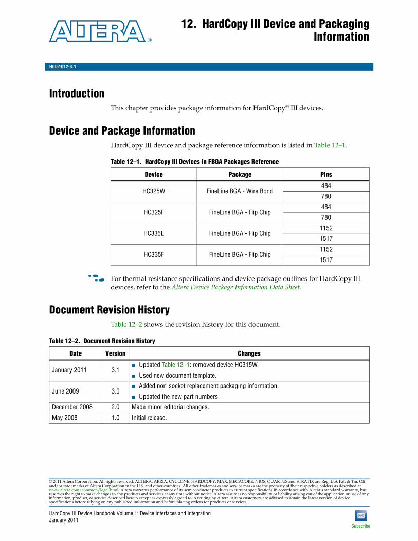
HardCopy III Device Handbook Volume 1: Device Interfaces and IntegrationJanuary 2011
HIII51012-3.1
Subscribe
© 2011 Altera Corporation. All rights reserved. ALTERA, ARRIA, CYCLONE, HARDCOPY, MAX, MEGACORE, NIOS, QUARTUS and STRATIX are Reg. U.S. Pat. & Tm. Off. and/or trademarks of Altera Corporation in the U.S. and other countries. All other trademarks and service marks are the property of their respective holders as described at www.altera.com/common/legal.html. Altera warrants performance of its semiconductor products to current specifications in accordance with Altera’s standard warranty, but reserves the right to make changes to any products and services at any time without notice. Altera assumes no responsibility or liability arising out of the application or use of any information, product, or service described herein except as expressly agreed to in writing by Altera. Altera customers are advised to obtain the latest version of device specifications before relying on any published information and before placing orders for products or services.
12. HardCopy III Device and PackagingInformation
IntroductionThis chapter provides package information for HardCopy® III devices.
Device and Package InformationHardCopy III device and package reference information is listed in Table 12–1.
f For thermal resistance specifications and device package outlines for HardCopy III devices, refer to the Altera Device Package Information Data Sheet.
Document Revision HistoryTable 12–2 shows the revision history for this document.
Table 12–1. HardCopy III Devices in FBGA Packages Reference
Device Package Pins
HC325W FineLine BGA - Wire Bond484
780
HC325F FineLine BGA - Flip Chip484
780
HC335L FineLine BGA - Flip Chip1152
1517
HC335F FineLine BGA - Flip Chip1152
1517
Table 12–2. Document Revision History
Date Version Changes
January 2011 3.1■ Updated Table 12–1: removed device HC315W.
■ Used new document template.
June 2009 3.0■ Added non-socket replacement packaging information.
■ Updated the new part numbers.
December 2008 2.0 Made minor editorial changes.
May 2008 1.0 Initial release.
January 2011HIII51012-3.1

12–2 Chapter 12: HardCopy III Device and Packaging InformationDocument Revision History
HardCopy III Device Handbook Volume 1: Device Interfaces and Integration January 2011 Altera Corporation

March 2012 Altera Corporation HardCopy III Device Handbook Volume 1: Device Interfaces and Integration
Additional Information
This chapter provides additional information about the document and Altera.
How to Contact AlteraTo locate the most up-to-date information about Altera products, refer to the following table.
Typographic ConventionsThe following table shows the typographic conventions this document uses.
Contact (1) Contact Method Address
Technical support Website www.altera.com/support
Technical trainingWebsite www.altera.com/training
Email [email protected]
Product literature Website www.altera.com/literature
Non-technical support (General) Email [email protected]
(Software Licensing) Email [email protected]
Note to Table:
(1) You can also contact your local Altera sales office or sales representative.
Visual Cue Meaning
Bold Type with Initial Capital Letters
Indicate command names, dialog box titles, dialog box options, and other GUI labels. For example, Save As dialog box. For GUI elements, capitalization matches the GUI.
bold typeIndicates directory names, project names, disk drive names, file names, file name extensions, software utility names, and GUI labels. For example, \qdesigns directory, D: drive, and chiptrip.gdf file.
Italic Type with Initial Capital Letters Indicate document titles. For example, Stratix IV Design Guidelines.
italic typeIndicates variables. For example, n + 1.
Variable names are enclosed in angle brackets (< >). For example, <file name> and <project name>.pof file.
Initial Capital Letters Indicate keyboard keys and menu names. For example, the Delete key and the Options menu.
“Subheading Title” Quotation marks indicate references to sections within a document and titles of Quartus II Help topics. For example, “Typographic Conventions.”

–2 Additional InformationTypographic Conventions
HardCopy III Device Handbook Volume 1: Device Interfaces and Integration March 2012 Altera Corporation
Courier type
Indicates signal, port, register, bit, block, and primitive names. For example, data1, tdi, and input. The suffix n denotes an active-low signal. For example, resetn.
Indicates command line commands and anything that must be typed exactly as it appears. For example, c:\qdesigns\tutorial\chiptrip.gdf.
Also indicates sections of an actual file, such as a Report File, references to parts of files (for example, the AHDL keyword SUBDESIGN), and logic function names (for example, TRI).
r An angled arrow instructs you to press the Enter key.
1., 2., 3., anda., b., c., and so on
Numbered steps indicate a list of items when the sequence of the items is important, such as the steps listed in a procedure.
■ ■ ■ Bullets indicate a list of items when the sequence of the items is not important.
1 The hand points to information that requires special attention.
h A question mark directs you to a software help system with related information.
f The feet direct you to another document or website with related information.
c A caution calls attention to a condition or possible situation that can damage or destroy the product or your work.
w A warning calls attention to a condition or possible situation that can cause you injury.
The envelope links to the Email Subscription Management Center page of the Altera website, where you can sign up to receive update notifications for Altera documents.
Visual Cue Meaning

101 Innovation DriveSan Jose, CA 95134www.altera.com
HC3_H5V2-3.3
Volume 2: Design Flow and Prototyping
HardCopy III Device Handbook,
HardCopy III Device Handbook, Volume 2: Design Flow and Prototyping

HardCopy III Device Handbook, Volume 2: Design Flow and Prototyping March 2012 Altera Corporation
© 2012 Altera Corporation. All rights reserved. ALTERA, ARRIA, CYCLONE, HARDCOPY, MAX, MEGACORE, NIOS, QUARTUS and STRATIX are Reg. U.S. Pat.& Tm. Off. and/or trademarks of Altera Corporation in the U.S. and other countries. All other trademarks and service marks are the property of their respectiveholders as described at www.altera.com/common/legal.html. Altera warrants performance of its semiconductor products to current specifications in accordancewith Altera’s standard warranty, but reserves the right to make changes to any products and services at any time without notice. Altera assumes no responsibility orliability arising out of the application or use of any information, product, or service described herein except as expressly agreed to in writing by Altera. Alteracustomers are advised to obtain the latest version of device specifications before relying on any published information and before placing orders for products orservices.

March 2012 Altera Corporation
Contents
Chapter Revision Dates . . . . . . . . . . . . . . . . . . . . . . . . . . . . . . . . . . . . . . . . . . . . . . . . . . . . . . . . . . . . . . . . . . . . . . . v
Section I. HardCopy III Design Flow and Prototyping with Stratix III Devices
Chapter 1. HardCopy III Design Flow Using the Quartus II SoftwareHardCopy III Development Flow . . . . . . . . . . . . . . . . . . . . . . . . . . . . . . . . . . . . . . . . . . . . . . . . . . . . . . . . . . 1–1
Designing with the Stratix III Device First Flow . . . . . . . . . . . . . . . . . . . . . . . . . . . . . . . . . . . . . . . . . . . 1–2Designing with the HardCopy III Device First Flow . . . . . . . . . . . . . . . . . . . . . . . . . . . . . . . . . . . . . . . 1–4
HardCopy Advisor . . . . . . . . . . . . . . . . . . . . . . . . . . . . . . . . . . . . . . . . . . . . . . . . . . . . . . . . . . . . . . . . . . . . . . 1–5FPGA and HardCopy Companion Device Planning . . . . . . . . . . . . . . . . . . . . . . . . . . . . . . . . . . . . . . . . . . 1–5
Logic Resources . . . . . . . . . . . . . . . . . . . . . . . . . . . . . . . . . . . . . . . . . . . . . . . . . . . . . . . . . . . . . . . . . . . . . . 1–5I/O Pin and Package Offering . . . . . . . . . . . . . . . . . . . . . . . . . . . . . . . . . . . . . . . . . . . . . . . . . . . . . . . . . . 1–5Memory Resources . . . . . . . . . . . . . . . . . . . . . . . . . . . . . . . . . . . . . . . . . . . . . . . . . . . . . . . . . . . . . . . . . . . . 1–8DSP Blocks Implementation . . . . . . . . . . . . . . . . . . . . . . . . . . . . . . . . . . . . . . . . . . . . . . . . . . . . . . . . . . . . 1–9
Clock and PLL Planning . . . . . . . . . . . . . . . . . . . . . . . . . . . . . . . . . . . . . . . . . . . . . . . . . . . . . . . . . . . . . . . . . . 1–9Clock Networks and PLL Resources . . . . . . . . . . . . . . . . . . . . . . . . . . . . . . . . . . . . . . . . . . . . . . . . . . . . . 1–9Add PLL Reconfiguration to Altera IP Blocks . . . . . . . . . . . . . . . . . . . . . . . . . . . . . . . . . . . . . . . . . . . . . 1–9Use Dedicated Clock Pins . . . . . . . . . . . . . . . . . . . . . . . . . . . . . . . . . . . . . . . . . . . . . . . . . . . . . . . . . . . . . 1–10
Quartus II Settings for HardCopy III Devices . . . . . . . . . . . . . . . . . . . . . . . . . . . . . . . . . . . . . . . . . . . . . . 1–10Limit DSP and RAM to HardCopy Device Resources . . . . . . . . . . . . . . . . . . . . . . . . . . . . . . . . . . . . . 1–10Enable Design Assistant to Run During Compile . . . . . . . . . . . . . . . . . . . . . . . . . . . . . . . . . . . . . . . . . 1–11I/O Assignment Settings . . . . . . . . . . . . . . . . . . . . . . . . . . . . . . . . . . . . . . . . . . . . . . . . . . . . . . . . . . . . . . 1–11Physical Synthesis Optimization Settings . . . . . . . . . . . . . . . . . . . . . . . . . . . . . . . . . . . . . . . . . . . . . . . . 1–13Timing Settings . . . . . . . . . . . . . . . . . . . . . . . . . . . . . . . . . . . . . . . . . . . . . . . . . . . . . . . . . . . . . . . . . . . . . . 1–14
Timing Constraints for the TimeQuest Timing Analyzer . . . . . . . . . . . . . . . . . . . . . . . . . . . . . . . . 1–14TimeQuest Multicorner Timing Analysis Setting . . . . . . . . . . . . . . . . . . . . . . . . . . . . . . . . . . . . . . . 1–15
Incremental Compilation . . . . . . . . . . . . . . . . . . . . . . . . . . . . . . . . . . . . . . . . . . . . . . . . . . . . . . . . . . . . . . . . 1–15Top-Down Incremental Compilation . . . . . . . . . . . . . . . . . . . . . . . . . . . . . . . . . . . . . . . . . . . . . . . . . . . 1–17Top-Down Incremental Compilation with Empty Design Partitions . . . . . . . . . . . . . . . . . . . . . . . . . 1–18
Quartus II Fitter Settings . . . . . . . . . . . . . . . . . . . . . . . . . . . . . . . . . . . . . . . . . . . . . . . . . . . . . . . . . . . . . . . . 1–19HardCopy Design Readiness Check . . . . . . . . . . . . . . . . . . . . . . . . . . . . . . . . . . . . . . . . . . . . . . . . . . . . . . . 1–20Timing Closure and Verification . . . . . . . . . . . . . . . . . . . . . . . . . . . . . . . . . . . . . . . . . . . . . . . . . . . . . . . . . . 1–21
Timing Closure with the TimeQuest Timing Analyzer . . . . . . . . . . . . . . . . . . . . . . . . . . . . . . . . . . . . 1–21Verification . . . . . . . . . . . . . . . . . . . . . . . . . . . . . . . . . . . . . . . . . . . . . . . . . . . . . . . . . . . . . . . . . . . . . . . . . 1–22
Engineering Change Order (ECO) . . . . . . . . . . . . . . . . . . . . . . . . . . . . . . . . . . . . . . . . . . . . . . . . . . . . . . . . 1–23Migrating One-to-One Changes . . . . . . . . . . . . . . . . . . . . . . . . . . . . . . . . . . . . . . . . . . . . . . . . . . . . . . . . 1–24Migrating Changes that Must be Implemented Differently . . . . . . . . . . . . . . . . . . . . . . . . . . . . . . . . . 1–24
HardCopy III Handoff Process . . . . . . . . . . . . . . . . . . . . . . . . . . . . . . . . . . . . . . . . . . . . . . . . . . . . . . . . . . . 1–26Document Revision History . . . . . . . . . . . . . . . . . . . . . . . . . . . . . . . . . . . . . . . . . . . . . . . . . . . . . . . . . . . . . 1–27
Chapter 2. HardCopy Design Center Implementation ProcessHardCopy III Back-End Design Flow . . . . . . . . . . . . . . . . . . . . . . . . . . . . . . . . . . . . . . . . . . . . . . . . . . . . . . . 2–1
Design Netlist Generation . . . . . . . . . . . . . . . . . . . . . . . . . . . . . . . . . . . . . . . . . . . . . . . . . . . . . . . . . . . . . . 2–2Design for Testability . . . . . . . . . . . . . . . . . . . . . . . . . . . . . . . . . . . . . . . . . . . . . . . . . . . . . . . . . . . . . . . . . . 2–2Clock Tree and Global Signal Insertion . . . . . . . . . . . . . . . . . . . . . . . . . . . . . . . . . . . . . . . . . . . . . . . . . . . 2–2Tie-Off Connections for Unused Resources . . . . . . . . . . . . . . . . . . . . . . . . . . . . . . . . . . . . . . . . . . . . . . . 2–2Formal Verification of the Processed Netlist . . . . . . . . . . . . . . . . . . . . . . . . . . . . . . . . . . . . . . . . . . . . . . 2–2Timing and Signal Integrity Driven Place and Route . . . . . . . . . . . . . . . . . . . . . . . . . . . . . . . . . . . . . . . 2–3
HardCopy III Device Handbook, Volume 2: Design Flow and Prototyping

iv Contents
Parasitic Extraction and Timing Analysis . . . . . . . . . . . . . . . . . . . . . . . . . . . . . . . . . . . . . . . . . . . . . . . . . 2–3Back-End Timing Closure . . . . . . . . . . . . . . . . . . . . . . . . . . . . . . . . . . . . . . . . . . . . . . . . . . . . . . . . . . . . . . 2–3Timing ECOs . . . . . . . . . . . . . . . . . . . . . . . . . . . . . . . . . . . . . . . . . . . . . . . . . . . . . . . . . . . . . . . . . . . . . . . . . 2–3Formal Verification of the Post-Layout Netlist . . . . . . . . . . . . . . . . . . . . . . . . . . . . . . . . . . . . . . . . . . . . 2–5Layout Verification . . . . . . . . . . . . . . . . . . . . . . . . . . . . . . . . . . . . . . . . . . . . . . . . . . . . . . . . . . . . . . . . . . . . 2–5Design Signoff . . . . . . . . . . . . . . . . . . . . . . . . . . . . . . . . . . . . . . . . . . . . . . . . . . . . . . . . . . . . . . . . . . . . . . . . 2–5
Conclusion . . . . . . . . . . . . . . . . . . . . . . . . . . . . . . . . . . . . . . . . . . . . . . . . . . . . . . . . . . . . . . . . . . . . . . . . . . . . . 2–5Document Revision History . . . . . . . . . . . . . . . . . . . . . . . . . . . . . . . . . . . . . . . . . . . . . . . . . . . . . . . . . . . . . . 2–5
Chapter 3. Mapping Stratix III Device Resources to HardCopy III DevicesHardCopy III and Stratix III Mapping Options . . . . . . . . . . . . . . . . . . . . . . . . . . . . . . . . . . . . . . . . . . . . . . 3–3Summary of Differences Between HardCopy III and Stratix III Devices . . . . . . . . . . . . . . . . . . . . . . . . . 3–7Designing with HardCopy III Core Supply Requirements . . . . . . . . . . . . . . . . . . . . . . . . . . . . . . . . . . . . . 3–8Designing with HardCopy III I/Os . . . . . . . . . . . . . . . . . . . . . . . . . . . . . . . . . . . . . . . . . . . . . . . . . . . . . . . . 3–8
Mapping HardCopy III and Stratix III I/Os and Modular I/O Banks . . . . . . . . . . . . . . . . . . . . . . . . . 3–9HardCopy III Supported I/O Standards . . . . . . . . . . . . . . . . . . . . . . . . . . . . . . . . . . . . . . . . . . . . . . . . 3–13External Memory Interface I/Os in Stratix III and HardCopy III Devices . . . . . . . . . . . . . . . . . . . . 3–15Mapping Stratix III High-Speed Differential I/O Interfaces with HardCopy III Devices . . . . . . . . 3–16
HardCopy III PLL Planning and Utilization . . . . . . . . . . . . . . . . . . . . . . . . . . . . . . . . . . . . . . . . . . . . . . . . 3–21HardCopy III Memory Blocks . . . . . . . . . . . . . . . . . . . . . . . . . . . . . . . . . . . . . . . . . . . . . . . . . . . . . . . . . . . . 3–23
MLAB Implementation . . . . . . . . . . . . . . . . . . . . . . . . . . . . . . . . . . . . . . . . . . . . . . . . . . . . . . . . . . . . . . . 3–24MLAB, M9K, and M144K Utilization . . . . . . . . . . . . . . . . . . . . . . . . . . . . . . . . . . . . . . . . . . . . . . . . . . . 3–24
Using JTAG Features in HardCopy III Devices . . . . . . . . . . . . . . . . . . . . . . . . . . . . . . . . . . . . . . . . . . . . . 3–24Power-Up and Configuration Pin Compatibility with Stratix III Devices . . . . . . . . . . . . . . . . . . . . . . . 3–25Revision History . . . . . . . . . . . . . . . . . . . . . . . . . . . . . . . . . . . . . . . . . . . . . . . . . . . . . . . . . . . . . . . . . . . . . . . 3–27
Chapter 4. Matching Stratix III Power and Configuration Requirements with HardCopy III DevicesHardCopy III Power-Up Options . . . . . . . . . . . . . . . . . . . . . . . . . . . . . . . . . . . . . . . . . . . . . . . . . . . . . . . . . . 4–1
Instant On (No Added Delay) . . . . . . . . . . . . . . . . . . . . . . . . . . . . . . . . . . . . . . . . . . . . . . . . . . . . . . . . . . 4–2Instant On After 50 ms Delay . . . . . . . . . . . . . . . . . . . . . . . . . . . . . . . . . . . . . . . . . . . . . . . . . . . . . . . . . . . 4–2Configuration Pin Compatibility . . . . . . . . . . . . . . . . . . . . . . . . . . . . . . . . . . . . . . . . . . . . . . . . . . . . . . . . 4–6
Examples of Mapping a Stratix FPGA Configuration to a HardCopy ASIC . . . . . . . . . . . . . . . . . . . . . . 4–8HardCopy III Device Replacing a Stand-Alone Stratix III Device . . . . . . . . . . . . . . . . . . . . . . . . . . . . 4–8HardCopy III Device Replacing a Stratix III Device in a Cascaded Configuration Chain . . . . . . . . 4–9HardCopy III Device Replacing a Stratix III Device Configured with a Microprocessor . . . . . . . . 4–10HardCopy III Device Replacing an FPGA Configured in a JTAG Chain . . . . . . . . . . . . . . . . . . . . . . 4–11
Document Revision History . . . . . . . . . . . . . . . . . . . . . . . . . . . . . . . . . . . . . . . . . . . . . . . . . . . . . . . . . . . . . 4–13
Additional InformationHow to Contact Altera . . . . . . . . . . . . . . . . . . . . . . . . . . . . . . . . . . . . . . . . . . . . . . . . . . . . . . . . . . . . . . . . Info–1Typographic Conventions . . . . . . . . . . . . . . . . . . . . . . . . . . . . . . . . . . . . . . . . . . . . . . . . . . . . . . . . . . . . . Info–1
HardCopy III Device Handbook, Volume 2: Design Flow and Prototyping March 2012 Altera Corporation

March 2012 Altera Corporation
Chapter Revision Dates
The chapters in this document, HardCopy III Device Handbook, Volume 2: Design Flow and Prototyping, were revised on the following dates. Where chapters or groups of chapters are available separately, part numbers are listed.
Chapter 1. HardCopy III Design Flow Using the Quartus II SoftwareRevised: March 2012Part Number: HIII53001-3.3
Chapter 2. HardCopy Design Center Implementation ProcessRevised: January 2011Part Number: HIII53002-2.1
Chapter 3. Mapping Stratix III Device Resources to HardCopy III DevicesRevised: March 2012Part Number: HIII53003-3.3
Chapter 4. Matching Stratix III Power and Configuration Requirements with HardCopy III DevicesRevised: March 2012Part Number: HIII53004-3.2
HardCopy III Device Handbook, Volume 2: Design Flow and Prototyping

vi Chapter Revision Dates
HardCopy III Device Handbook, Volume 2: Design Flow and Prototyping March 2012 Altera Corporation
March 2012 Altera Corporation
Section I. HardCopy III Design Flow andPrototyping with Stratix III Devices
This section provides a description of the design flow and the implementation process used by the HardCopy Design Center. It also provides information about mapping Stratix® III devices to HardCopy® III devices and associated power and configuration requirements. This section includes the following chapters:
■ Chapter 1, HardCopy III Design Flow Using the Quartus II Software
■ Chapter 2, HardCopy Design Center Implementation Process
■ Chapter 3, Mapping Stratix III Device Resources to HardCopy III Devices
■ Chapter 4, Matching Stratix III Power and Configuration Requirements with HardCopy III Devices
Revision HistoryRefer to each chapter for its own specific revision history. For information on when each chapter was updated, refer to the Chapter Revision Dates section, which appears in the full handbook.
HardCopy III Device Handbook, Volume 2: Design Flow and Prototyping

I–2 Section I: HardCopy III Design Flow and Prototyping with Stratix III Devices
HardCopy III Device Handbook, Volume 2: Design Flow and Prototyping March 2012 Altera Corporation
HardCopy III Device Handbook, Volume 2: Design FloMarch 2012
HIII53001-3.3
© 2012 Altera Corporation. All rights reserved. ALTERA, ARRand/or trademarks of Altera Corporation in the U.S. and otherwww.altera.com/common/legal.html. Altera warrants performreserves the right to make changes to any products and servicesinformation, product, or service described herein except as expspecifications before relying on any published information and
March 2012HIII53001-3.3
1. HardCopy III Design Flow Using theQuartus II Software
This chapter provides recommendations for HardCopy® III development, planning, and settings considerations in the Quartus® II software. HardCopy III ASIC devices are Altera’s low-cost, high-performance, and low-power ASICs with pin-outs, densities, and architecture that complement Stratix® III FPGA devices. Using the Quartus II software, you can design with one set of register transfer level (RTL) code and one IP set for both Stratix III and HardCopy III implementations. This information helps ensure that your design mapping from the Stratix III FPGA to the HardCopy III ASIC is successful.
In the Quartus II software version 10.1 SP1, both companion and compilation for the HardCopy III family are supported. When you select a HardCopy III device from the Quartus II software, the Stratix III device is compatible with the HardCopy III device in the areas of pins, I/O standards, logic, and other resources.
HardCopy III Development FlowIn the Quartus II software, two methods are available for the HardCopy III development flow: Stratix III device first flow and HardCopy III device first flow.
■ Stratix III device first flow—Design the Stratix III device first for system functional verification and then create the HardCopy III companion device. Performing system verification early helps reduce overall total project development time.
■ HardCopy III device first flow—Design the HardCopy III device first and then create the Stratix III companion device for system functional verification. This method more accurately predicts the maximum performance of the HardCopy III ASIC during development. If you optimize your design to maximize HardCopy III ASIC performance, but are unable to meet your performance requirements with the Stratix III FPGA, you can still map your design with decreased performance requirements for in-system verification.
1 Whichever design flow you choose for your HardCopy III development, both the target design and the companion device design must be in one Quartus II project.
w and Prototyping
Subscribe
IA, CYCLONE, HARDCOPY, MAX, MEGACORE, NIOS, QUARTUS and STRATIX are Reg. U.S. Pat. & Tm. Off. countries. All other trademarks and service marks are the property of their respective holders as described at
ance of its semiconductor products to current specifications in accordance with Altera’s standard warranty, but at any time without notice. Altera assumes no responsibility or liability arising out of the application or use of any ressly agreed to in writing by Altera. Altera customers are advised to obtain the latest version of device before placing orders for products or services.

1–2 Chapter 1: HardCopy III Design Flow Using the Quartus II SoftwareHardCopy III Development Flow
Designing with the Stratix III Device First FlowThe HardCopy III development flow beginning with the Stratix III prototype is very similar to a traditional Stratix III design flow, but requires that you perform a few additional tasks to map the design to the HardCopy III companion device:
1. Choose a Stratix III device for prototyping.
2. Specify a HardCopy III device for conversion.
3. Compile the Stratix III design.
4. Create and compile the HardCopy III companion revision.
5. Compare the HardCopy III companion revision compilation to the Stratix III device compilation.
6. Generate the handoff files and reports.
7. Archive the design and send it to Altera to start the back-end design process.
HardCopy III Device Handbook, Volume 2: Design Flow and Prototyping March 2012 Altera Corporation

Chapter 1: HardCopy III Design Flow Using the Quartus II Software 1–3HardCopy III Development Flow
Figure 1–1 shows the development process for designing with a Stratix III device first and creating a HardCopy III companion device second.
Figure 1–1. Designing with the Stratix III Device First Flow
Prepare Stratix III Design
Archive Project for Handoff
Design Submission & Back-End Implementation Phase
Select HardCopy III Companion Device
Review HardCopy Advisor
Apply Design Constraints
Compile Stratix III Design
AnyViolations?
AnyViolations?
Create or Overwrite HardCopy IIICompanion Revision
Compile HardCopy III Companion Revision
Fits inHardCopy III Device?
Compare Stratix III & HardCopy III Revisions
Generate Handoff Report
HardCopy III Device Development with the Stratix III Device First Flow
In-System Verification
Select a LargerHardCopy III Companion
Device?
Fix ViolationsYes
No
Yes
Yes
No
No
March 2012 Altera Corporation HardCopy III Device Handbook, Volume 2: Design Flow and Prototyping

1–4 Chapter 1: HardCopy III Design Flow Using the Quartus II SoftwareHardCopy III Development Flow
Designing with the HardCopy III Device First FlowDesigning with the HardCopy III device first flow in the Quartus II software allows you to maximize performance in the HardCopy III device and map the design to the Stratix III prototype for in-system verification. The performance of the Stratix III prototype may be less than the HardCopy III device. For this design flow, you must select HardCopy III as the target device and Stratix III as the companion device in the Device Settings dialog box. The remaining tasks required to complete your design are outlined in Figure 1–2. The HardCopy Advisor adjusts its list of tasks based on the device family you start with to guide you through the development process.
Figure 1–2. Designing with the HardCopy III Device First Flow
Prepare HardCopy III Design
Design Submission & Back-End Implementation Phase
Select Stratix III Companion Device
Review HardCopy Advisor
Apply Design Constraints
Compile HardCopy III Design
AnyViolations?
AnyViolations?
Create or Overwrite Stratix IIICompanion Revision
Compile Stratix III Companion Revision
Compare Stratix III & HardCopy III Revisions
Generate Handoff Report
HardCopy III Device Development with the HardCopy III Device First Flow
In-System Verification
Fix ViolationsYes
No
Yes
No
Archive Project for Handoff
HardCopy III Device Handbook, Volume 2: Design Flow and Prototyping March 2012 Altera Corporation

Chapter 1: HardCopy III Design Flow Using the Quartus II Software 1–5HardCopy Advisor
HardCopy AdvisorThe HardCopy Advisor in the Quartus II software plays an important role in HardCopy III device development. The HardCopy Advisor guides you through a sequence of recommendations, descriptions, and actions. You can track your design progress, generate the design, and complete the comparison archiving and handoff file that you send to the Altera® HardCopy Design Center.
1 To develop the HardCopy III design, run the HardCopy Advisor in the Quartus II software after you select the Stratix III device and the HardCopy III companion devices. To run the HardCopy Advisor, on the Project menu, point to HardCopy Utilities and click HardCopy Advisor.
FPGA and HardCopy Companion Device PlanningFor both the HardCopy III device and Stratix III prototype planning, the first stage is to choose the device family, device density, speed grade, and package that best suits your design needs. Assuming a Stratix III device first flow, select the Stratix III device and HardCopy III companion device based on the best resource balance for your design requirements. Perform this task before compiling your design in a third-party synthesis tool or the Quartus II software.
f For information about the features available in each device density, including logic, memory blocks, multipliers, and phase-locked loops (PLLs), as well as the various package offerings and I/O pin counts, refer to volume 1 of the HardCopy III Device Handbook.
Logic ResourcesDuring HardCopy III device planning, determine the required logic density of the Stratix III prototype and HardCopy III companion device. Devices with more logic resources can implement larger and potentially more complex designs. Smaller devices have less logic resources available and benefit from lower power consumption. Select a device that meets your design needs with some margin, in case you want to add more logic later in the design cycle.
f For information about logic resources in HardCopy III devices, refer to the HardCopy III Device Family Overview chapter.
I/O Pin and Package OfferingHardCopy III devices offer pin-to-pin compatibility with Stratix III prototypes, making them drop-in replacements for FPGAs. Due to this compatibility, the same system board and software developed for the FPGA prototype can be retained, enabling faster time to market for high volume production.
HardCopy III devices also offer non-socket replacement mapping for further cost reductions. For example, you can map the EP3SL110 device in the 780-pin FBGA package to the HC325 device in the 484-pin FBGA package. Because the pinout for the two packages are not the same, a separate board design is required for the Stratix III device and the HardCopy III device.
March 2012 Altera Corporation HardCopy III Device Handbook, Volume 2: Design Flow and Prototyping

1–6 Chapter 1: HardCopy III Design Flow Using the Quartus II SoftwareFPGA and HardCopy Companion Device Planning
f For the non-socket replacement path, be sure to select I/Os in the Stratix III device that can be mapped to the HardCopy III device. Not all I/Os in the Stratix III device are available in the HardCopy III non-socket replacement device. Check the pinout information for both the Stratix III device and the HardCopy III device to ensure that you can map successfully and be sure to select the HardCopy III companion device when designing for the Stratix III device.
When mapping a specific Stratix III device to a HardCopy III companion device, there are a number of FPGA prototype choices. Table 1–1 shows the mapping options for the Stratix III prototype and HardCopy III companion device by package.
HardCopy III Device Handbook, Volume 2: Design Flow and Prototyping March 2012 Altera Corporation

Chapter 1:HardCopy III Design Flow
Using the Quartus II Software
1–7FPGA and HardCopy Com
panion Device Planning
March 2012
Altera CorporationHardCopy III Device Handbook, Volum
e 2: Design Flow and Prototyping
1)
SE260 EP3SL340
152 F1517 H1152 F1517
— — (2) —
— — (2) —
— (3) —
— —
gular FBGA package.
Table 1–1. Stratix III FPGA to HardCopy III ASIC Mapping Paths
HardCopy III ASIC Stratix III FPGA Prototype and Package (Note
Device PackageEP3SL110 EP3SL150 EP3SE110 EP3SL200 EP3
F780 F780 F1152 F780 F1152 H780 F1152 F1517 H780 F1
HC325
484-pin FineLine BGA (2) (2) — (2) — (2) — — (2)
780-pin FineLine BGA — — (3) — — (3)
HC335
1152-pin FineLine BGA — — — — — —
1517-pin FineLine BGA — — — — — — — —
Notes to Table 1–1:
(1) HardCopy III device migration paths are not supported for the EP3SL50, EP3SL70, EP3SE50, and EP3SE80 Stratix III devices.(2) This mapping is a non-socket replacement path that requires a different board design for the Stratix III device and the HardCopy III device.(3) The Hybrid FBGA package requires additional unused board space along the edges beyond the footprint, but its footprint is compatible with the re

1–8 Chapter 1: HardCopy III Design Flow Using the Quartus II SoftwareFPGA and HardCopy Companion Device Planning
f For more information about I/O features in HardCopy III devices, refer to the HardCopy III Device I/O Features chapter in volume 1 of the HardCopy III Device Handbook.
f For more information about HardCopy III device packages, refer to the HardCopy III Device Family Overview chapter in volume 1 of the HardCopy III Device Handbook.
Memory ResourcesThe TriMatrix memory in HardCopy III devices supports the same memory functions and features as Stratix III devices. You can configure each embedded memory block to be a single- or dual-port RAM, FIFO, ROM, or shift register using the MegaWizard™ Plug-In Manager in the Quartus II software.
HardCopy III embedded memory consists of memory logic array blocks (MLABs), M9K, and M144K memory blocks and has a one-to-one mapping from the Stratix III memory. However, the number of available memory blocks differs based on density, package, and Stratix III FPGA-to-HardCopy III ASIC mapping paths.
f For more information about HardCopy III embedded memory resources, refer to the Mapping Stratix III Device Resources with HardCopy III Devices chapter.
While all three memory types are dedicated resources in Stratix III devices, only the M9K and M144K memory blocks are dedicated resources in the HardCopy III devices. However, the same functionality of the Stratix III MLABs can be supported in HardCopy III devices. The Quartus II software maps the Stratix III MLAB function to the appropriate HCell macro that preserves the memory function. This allows the HardCopy III core fabric to be used more efficiently, freeing up unused HCells for adaptive logic modules (ALMs) or digital signal processing (DSP) functions.
Although the memory in HardCopy III devices supports the same memory functions and features as Stratix III devices, you cannot pre-load or initialize HardCopy III memory blocks with a Memory Initialization File (.mif) when they are used as RAM. Unlike Stratix III devices, HardCopy III devices do not have device configuration. The memory content of HardCopy III devices are random after power-up. Therefore, you must ensure that your Stratix III design does not require a .mif if the memory blocks are used as RAM. However, if the HardCopy III memory block is designed as ROM, it powers up with the ROM contents.
1 Use the ALTMEM_INIT megafunction to initialize the RAM after power-up for HardCopy III devices. This megafunction reads from an internal ROM (inside the megafunction) or an external ROM (on-chip or off-chip) and writes to the RAM after power-up.
When using non-registered output mode for the HardCopy III MLABs, the output powers up with memory content. When using registered output mode for these memory blocks, the outputs are cleared on power-up. You must take this into consideration when designing logic that might evaluate the initial power-up values of the MLAB memory block.
f For more information about memory blocks in HardCopy III devices, refer to the TriMatrix Embedded Memory Blocks in HardCopy III Devices chapter.
HardCopy III Device Handbook, Volume 2: Design Flow and Prototyping March 2012 Altera Corporation

Chapter 1: HardCopy III Design Flow Using the Quartus II Software 1–9Clock and PLL Planning
DSP Blocks ImplementationThe Quartus II software uses a library of pre-characterized HCell macros to place Stratix III DSP configurations into the HardCopy III HCell-based logic fabric. Depending on the Stratix III DSP configurations, the Quartus II software partitions the DSP function into a combination of DSP HCell macros in the HardCopy III device. This optimizes the DSP function and allows the core fabric to be used more efficiently.
f For more information about DSP blocks in HardCopy III devices, refer to the DSP Blocks Implementation in HardCopy III Devices chapter.
Clock and PLL PlanningTo ensure that you map the Stratix III design to a HardCopy III design successfully, follow these guidelines when implementing your design. They can help make your design robust, ensuring it meets timing closure and achieves the performance you need.
f For more information about clock scheme and PLL features in HardCopy III devices, refer to the Clock Networks and PLLs in HardCopy III Devices chapter.
Clock Networks and PLL Resources You must consider the system clocking scheme, timing requirements, and fan-out requirements during clock networks and PLL resources planning. Matching PLL resources between Stratix III and HardCopy III devices is determined by the design’s clocking scheme and timing requirements. For high fan-out signals, use a dedicated clock resource.
In the Quartus II software, be sure the HardCopy III companion device is selected in the device selection panel. This ensures that the PLL, other resources used, and the functions implemented in both the Stratix III and HardCopy III designs match. In addition, it ensures that the design converts successfully.
f For more information about HardCopy III PLL resources, refer to the Mapping Stratix III Device Resources with HardCopy III Devices chapter.
Add PLL Reconfiguration to Altera IP BlocksEnable PLL reconfiguration for your design if it uses PLLs. The PLL settings in HardCopy III companion devices may require different settings from the Stratix III PLLs because of different clock tree lengths and PLL compensations. By enabling PLL reconfiguration, you can adjust your PLL settings on the HardCopy III companion device after the silicon has been fabricated. This allows you to fine tune and further optimize your system performance.
f For information about implementing PLL reconfiguration in Stratix III FPGAs, refer to AN 454: Implementing PLL Reconfiguration in Stratix III Devices.
March 2012 Altera Corporation HardCopy III Device Handbook, Volume 2: Design Flow and Prototyping

1–10 Chapter 1: HardCopy III Design Flow Using the Quartus II SoftwareQuartus II Settings for HardCopy III Devices
Use Dedicated Clock PinsDuring clock planning, use dedicated clock input pins for high fan-out control signals, such as asynchronous clears, presets, and clock enables for protocol signals, such as TRDY and IRDY for PCI Express (PIPE), in global or regional clock networks. These dedicated routing networks provide predictable delay and minimize skew for high fan-out signals.
Use dedicated clock pins to drive the PLL reference clock inputs, especially if the design interfaces with external memories. This minimizes the reference clock input jitter to the PLLs, providing more timing margin to make the timing closure successful. For external memory interfaces, Altera recommends using the double date rate (DDR) register in the I/O element to generate the external memory clocks.
f For information about external memory interfaces, refer to the External Memory Interfaces in HardCopy III Devices chapter.
Quartus II Settings for HardCopy III DevicesThe HardCopy III development flow requires additional Quartus II settings when compared with a typical FPGA-only design flow. This is because the HardCopy III design is implemented in two devices: a Stratix III prototype and a HardCopy III companion device. You must take these settings into consideration when developing your design.
Limit DSP and RAM to HardCopy Device ResourcesTo maintain compatibility between the Stratix III and HardCopy III devices, your design must use resources that are common to both families. The Quartus II software turns on Limit DSP & RAM to HardCopy device resources by default when you select the Stratix III device and HardCopy III companion device in the Quartus II software. This prevents the Quartus II software from using resources in the Stratix III device that are not available in the HardCopy III device.
Figure 1–3 shows the appropriate setting to select in the Companion device section.
1 The Altera HardCopy Design Center requires that your final Stratix III and HardCopy III designs be compiled with the Limit DSP & RAM to HardCopy device resources setting turned on before submission to the Altera HardCopy Design Center for back-end implementation.
Figure 1–3. Limit DSP and RAM to HardCopy III Device Resources Checkbox
HardCopy III Device Handbook, Volume 2: Design Flow and Prototyping March 2012 Altera Corporation

Chapter 1: HardCopy III Design Flow Using the Quartus II Software 1–11Quartus II Settings for HardCopy III Devices
Enable Design Assistant to Run During CompileYou must use the Quartus II Design Assistant to check for design rule violations before submitting the designs to the Altera HardCopy Design Center. Additionally, you must fix all critical and high-level errors reported by the Quartus II Design Assistant. Altera recommends turning on the Design Assistant to run automatically during development.
To enable the Design Assistant to run during compilation, on the Assignments menu, click Settings. In the Category list, select Design Assistant and turn on Run Design Assistant during compilation.
Figure 1–4 shows the Design Assistant.
I/O Assignment SettingsDue to the complex rules governing the use of I/O cells and their availability for specific pins and packages, Altera recommends that I/O assignments be completed using the Pin Planner tool and the Assignment Editor in the Quartus II software. These tools ensure that all of the rules regarding each pin and I/O cell are applied correctly. The Quartus II software can export a .Tcl script containing all I/O assignments.
f For more information about I/O location and type assignments using the Quartus II Assignment Editor and Pin Planner tools, refer to the Assignment Editor chapter in volume 2 of the Quartus II Handbook.
Figure 1–4. Enabling the Design Assistant
March 2012 Altera Corporation HardCopy III Device Handbook, Volume 2: Design Flow and Prototyping

1–12 Chapter 1: HardCopy III Design Flow Using the Quartus II SoftwareQuartus II Settings for HardCopy III Devices
To ensure that the HardCopy III mapping is successful, you must make accurate I/O assignments that include pin locations, I/O standards, drive strengths, and capacitance loading for the design. Ensure that the I/O assignments are compatible with all selected devices. Altera recommends not leaving any I/O with an unassigned I/O assignment.
The I/O pins of a Stratix III device and a HardCopy III device are arranged in groups called modular I/O banks. When mapping between a Stratix III device and a HardCopy III device, the I/O pin location must be assigned to the available common I/O banks for both devices. Because HardCopy III devices have fewer I/O banks than Stratix III devices, the Quartus II software limits the I/O banks to only those available in HardCopy III devices.
f For more information about I/O banks and pins in HardCopy III devices, refer to the HardCopy III Device I/O Features chapter.
HardCopy III I/O buffers can only support the 3.0 V I/O standard with a maximum VCCIO of 3.0 V. Therefore, when specifying the I/O standard for the Stratix III FPGA device with the HardCopy III companion device already selected, make sure to choose an I/O standard with a VCCIO of 3.0 V or below. Selecting an I/O standard that requires a VCCIO of 3.3 V results in a compilation error.
f For more information about HardCopy III I/O buffers and the standards they support, refer to the DC and Switching Characteristics chapter.
It is essential to constrain the I/O standards for the design. If you leave the I/O with an unassigned I/O assignment, the Quartus II software assigns the I/O standard to 2.5 V by default. This standard may not be compatible with your intended I/O standard. To check the supported I/O standards and identify incompatible I/O settings on the assigned I/Os, run the Quartus II I/O Assignment Analysis to verify the I/O settings and assignments. To run I/O Assignment Analysis, on the Processing menu, point to Start, then click Start I/O Assignment Analysis.
HardCopy III Device Handbook, Volume 2: Design Flow and Prototyping March 2012 Altera Corporation

Chapter 1: HardCopy III Design Flow Using the Quartus II Software 1–13Quartus II Settings for HardCopy III Devices
Figure 1–5 shows the I/O assignment analysis in the Quartus II software.
The default output drive strength in the Quartus II software might not be appropriate for your application. Altera recommends verifying the correct output drive strength for the design. Assigning the right output drive strength improves signal integrity while achieving timing requirements. In addition, the output capacitance loading for both the output and bidirectional pins must be set in the I/O assignment for a successful HardCopy compilation.
Physical Synthesis Optimization SettingsWhen you develop a HardCopy III device with the Quartus II software, you can target physical synthesis optimizations to the FPGA architecture in Stratix III-device first flow or the HardCopy architecture in the HardCopy III-first flow. The optimizations in the base revision are mapped to the companion device architecture during the mapping process and the post-fitting netlists of both devices are generated and compared. Therefore, you must have the identical physical synthesis settings for both the HardCopy III ASIC and Stratix III FPGA revisions in order to avoid revision comparison failure.
To enable Physical Synthesis Optimizations for the Stratix III FPGA revision of the design, on the Assignments menu, click Settings. In the Settings dialog box, in the Category list, expand Fitter Settings. These optimizations are passed into the HardCopy III companion revision for placement and timing closure. When designing with a HardCopy III device first, you can enable physical synthesis optimizations for the HardCopy III device, and these post-fit optimizations are passed to the Stratix III FPGA revision.
Figure 1–5. Start I/O Assignment Analysis
March 2012 Altera Corporation HardCopy III Device Handbook, Volume 2: Design Flow and Prototyping

1–14 Chapter 1: HardCopy III Design Flow Using the Quartus II SoftwareQuartus II Settings for HardCopy III Devices
1 Beginning with the Quartus II v9.0 software, the Physical Synthesis Optimizations settings changed. If a HardCopy III device is set as a companion device, the Physical Synthesis Optimization setting in the Stratix III FPGA or HardCopy III ASIC revision supports the Perform physical synthesis for combination logic and Perform register retiming options. In addition, the effort level of physical synthesis optimization is set to Fast by default.
Timing SettingsFor HardCopy III device development, you must use the TimeQuest Timing Analyzer. In the Quartus II software, TimeQuest Timing Analyzer is the default timing analyzer for Stratix III and HardCopy III designs. The TimeQuest Timing Analyzer guides the Quartus II Fitter and analyzes timing results during each Stratix III and HardCopy III design compilation.
For information about how to set the Quartus II Fitter to use timing-driven compilation, refer to “Quartus II Fitter Settings” on page 1–19.
Timing Constraints for the TimeQuest Timing AnalyzerThe TimeQuest Timing Analyzer is a powerful ASIC-style timing analysis tool that validates timing in your design using industry-standard constraint, analysis, and reporting methodology. You can use the TimeQuest analyzer’s GUI or command-line interface to constrain, analyze, and report results for all timing paths in your design.
Before running the TimeQuest analyzer, you must specify initial timing constraints that describe the clock characteristics, timing exceptions, signal transition arrival, and required times. You can specify timing constraints in the Synopsys Design Constraints File (.sdc) format using the TimeQuest analyzer GUI or the command-line interface. The Quartus II Fitter optimizes the placement of logic to meet your constraints.
The TimeQuest analyzer analyzes the timing paths in the design, calculates the propagation delay along each path, checks for timing constraint violations, and reports timing results as slack in the Report and Console panels. If the TimeQuest analyzer reports any timing violations, you can customize the reporting to view precise timing information about the specific paths, and then constrain those paths to correct the violations. When your design is free of timing violations, you can be confident that the logic will operate as intended in the target device.
The TimeQuest analyzer is a complete static timing analysis tool that you can use as a sign-off tool for the Stratix III design. For the HardCopy III design, the Altera HardCopy Design Center uses the PrimeTime timing analyzer as the sign-off tool for back-end implementation.
f For more information about how to create .sdc format timing constraints, refer to the Quartus II TimeQuest Timing Analyzer chapter in volume 3 of the Quartus II Handbook.
HardCopy III Device Handbook, Volume 2: Design Flow and Prototyping March 2012 Altera Corporation

Chapter 1: HardCopy III Design Flow Using the Quartus II Software 1–15Incremental Compilation
TimeQuest Multicorner Timing Analysis SettingThe Altera HardCopy Design Center requires that all HardCopy handoff files include a TimeQuest analyzer timing report for design review. In the TimeQuest analyzer timing report, you must include both fast- and slow-corner timing analysis for setup, hold, and I/O paths. To do this, enable the Multicorner timing analysis during compilation option on the TimeQuest Timing Analyzer page in the Quartus II software. This option directs the TimeQuest analyzer to analyze the design and generate slack reports for the slow and fast corners. Figure 1–6 shows the settings you must enable so that the TimeQuest analyzer generates the appropriate reports.
Incremental CompilationFor the HardCopy development flow, the Quartus II design software offers incremental compilation to preserve the compilation results for unchanged logic in your design. This feature dramatically reduces your design iteration time by focusing new compilations only on changed design partitions. New compilation results are then merged with the previous compilation results from unchanged design partitions.
There are two approaches of incremental compilation in the Quartus II software:
■ Top-down incremental compilation
■ Bottom-up incremental compilation
1 Bottom-up incremental compilation flow is not supported for designs targeting HardCopy ASICs.
Figure 1–6. TimeQuest Multicorner Timing Analysis Setting
March 2012 Altera Corporation HardCopy III Device Handbook, Volume 2: Design Flow and Prototyping

1–16 Chapter 1: HardCopy III Design Flow Using the Quartus II SoftwareIncremental Compilation
For large, high-density and high-performance designs in Stratix FPGAs and HardCopy ASICs, use top-down incremental compilation. Top-down incremental compilation facilitates team-based design environments, allowing designers to create and optimize design blocks independently. Begin planning for incremental compilation from the start of your design development. To take advantage of incremental compilation flow, split the design along any of its hierarchical boundaries into blocks called design partitions.
In the Quartus II software, the same procedures create design partitions in the HardCopy ASIC and Stratix FPGA revisions.
f For more information about creating design partitions, refer to the Quartus II Incremental Compilation for Hierarchical and Team-Based Design chapter in volume 1 of the Quartus II Handbook.
In the Quartus II software, the full Incremental Compilation option is on by default, so the project is ready for you to create design partitions for incremental compilation. Figure 1–7 shows the full Incremental Compilation page in the Quartus II software.
1 If you do not create design partitions in a design, the Quartus II software uses a flat compilation flow, and you cannot use Incremental Compilation.
Figure 1–7. Quartus II Incremental Compilation Option
HardCopy III Device Handbook, Volume 2: Design Flow and Prototyping March 2012 Altera Corporation

Chapter 1: HardCopy III Design Flow Using the Quartus II Software 1–17Incremental Compilation
Top-Down Incremental CompilationTop-down incremental compilation is supported for the base revision for designs targeting HardCopy ASICs in both the FPGA first flow and HardCopy first flow. In the Quartus II design software, you must select the base and companion revisions before design partitions of the base revision are created.
After the design partitions are created in the Quartus II design software, the base revision is compiled and the design partition assignments are mapped to the companion device. In the HardCopy development flow, you make changes only in the base revision's design and design partition assignments with the Quartus II design software. Therefore, you can perform top-down incremental compilation only in the base revision, but cannot perform incremental compilation to the companion revision. Figure 1–8 shows the design “Top” with two design partitions.
After the design partitions are created and compiled in the base family revision, you can modify the specific design partitions for additional area and performance improvement. Figure 1–9 shows that when the logic is modified in partition “inst3” the Quartus II software is ready to re-compile the individual hierarchical design partition separately, based on the preservation level in the Design Partition Window. Therefore, the optimization result of design partitions “top” and “inst2” are preserved while the partition “inst3” is re-compiled in the Quartus II design software.
Figure 1–8. Quartus II Project with Design Partitions
Figure 1–9. Design Partition Modified
Partition “inst3” Partition “inst2”
Top
Partition “inst3” Partition “inst2”(No Change)
Top
March 2012 Altera Corporation HardCopy III Device Handbook, Volume 2: Design Flow and Prototyping

1–18 Chapter 1: HardCopy III Design Flow Using the Quartus II SoftwareIncremental Compilation
Before recompiling the design, you can set the Netlist Type in the Design Partition Window to Source File, Post-Synthesis, or Post-Fitting to preserve the Netlist Type of each design partition. Figure 1–10 shows the Design Partition Window with the Post-Fit preservation level for the design partitions “top” and “inst2.” This allows the Quartus II design software to re-compile the design partition “inst2” from the source file, but preserves the post-fitting results of design partitions “top” and “inst3.”
The Quartus II software merges the new compiled design partition “inst3” into a complete netlist for subsequent stages of the compilation flow. Design partitions “top” and “inst2” in the design do not perform incremental compilation because their logic must be preserved. Therefore, the compilation time for the overall design is reduced.
Top-Down Incremental Compilation with Empty Design PartitionsBottom-up incremental compilation is not supported in the HardCopy development flow. During the initial stage of the design cycle, part of the design may be incomplete or developed by a different designer or IP provider. However, you can create an empty partition for this part of the design while compiling the completed partitions, and then save the results for the complete partitions while you optimize the imported part of the design.
1 You can often use a top-down flow with empty partitions to implement behavior similar to a bottom-up flow, as long as you do not change the global assignments between compilations. All global assignments must be the same for all compiled partitions, so the assignments can be reproduced in the companion device after mapping.
1 For the HardCopy development flow, create an empty partition in the base device because it cannot be created in the companion revision.
Creating an empty partition in a design is similar to creating a regular design partition in the Quartus II software. When the logic within a specific design partition is incomplete, use the following instructions to set the Netlist Type to Empty.
1. On the Assignment menu, click Design Partitions Window.
2. Double-click an entry under the Netlist Type column and select Empty.
Figure 1–10. Design Partition Window
HardCopy III Device Handbook, Volume 2: Design Flow and Prototyping March 2012 Altera Corporation
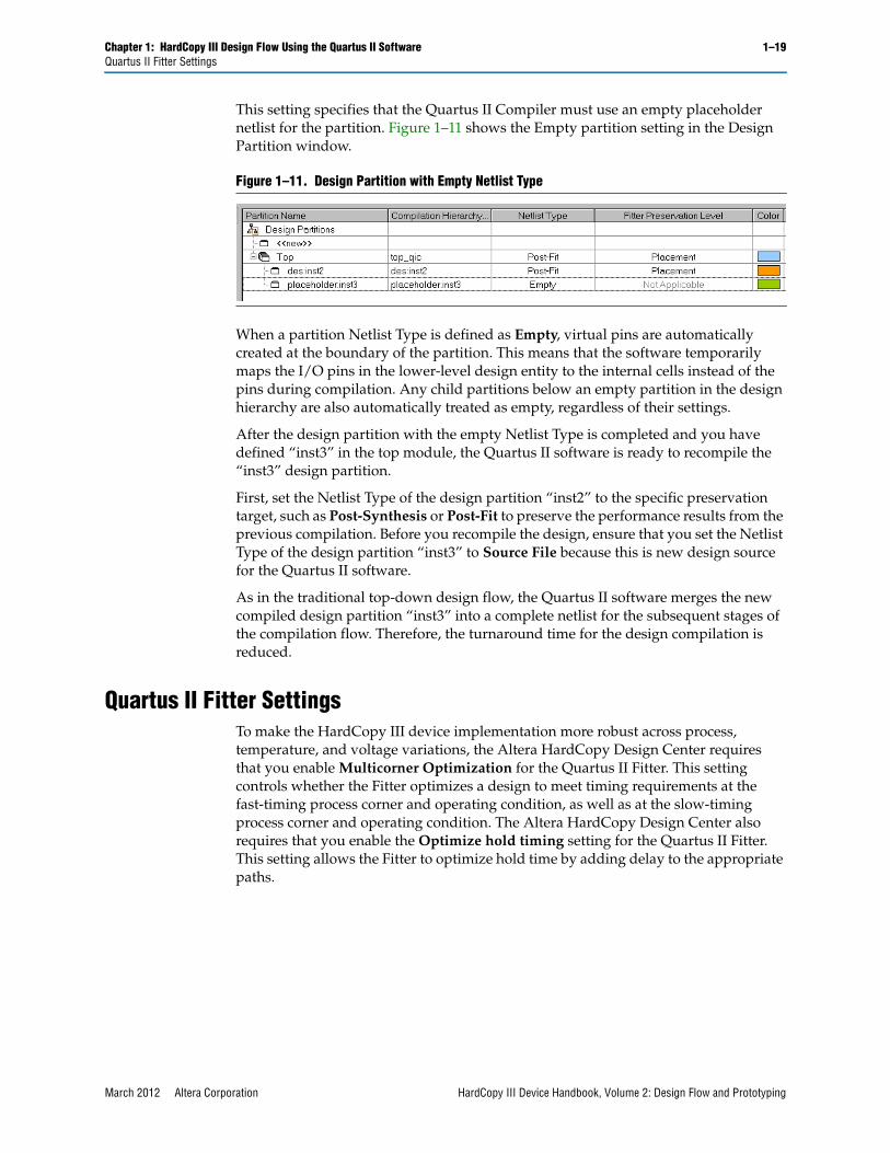
Chapter 1: HardCopy III Design Flow Using the Quartus II Software 1–19Quartus II Fitter Settings
This setting specifies that the Quartus II Compiler must use an empty placeholder netlist for the partition. Figure 1–11 shows the Empty partition setting in the Design Partition window.
When a partition Netlist Type is defined as Empty, virtual pins are automatically created at the boundary of the partition. This means that the software temporarily maps the I/O pins in the lower-level design entity to the internal cells instead of the pins during compilation. Any child partitions below an empty partition in the design hierarchy are also automatically treated as empty, regardless of their settings.
After the design partition with the empty Netlist Type is completed and you have defined “inst3” in the top module, the Quartus II software is ready to recompile the “inst3” design partition.
First, set the Netlist Type of the design partition “inst2” to the specific preservation target, such as Post-Synthesis or Post-Fit to preserve the performance results from the previous compilation. Before you recompile the design, ensure that you set the Netlist Type of the design partition “inst3” to Source File because this is new design source for the Quartus II software.
As in the traditional top-down design flow, the Quartus II software merges the new compiled design partition “inst3” into a complete netlist for the subsequent stages of the compilation flow. Therefore, the turnaround time for the design compilation is reduced.
Quartus II Fitter SettingsTo make the HardCopy III device implementation more robust across process, temperature, and voltage variations, the Altera HardCopy Design Center requires that you enable Multicorner Optimization for the Quartus II Fitter. This setting controls whether the Fitter optimizes a design to meet timing requirements at the fast-timing process corner and operating condition, as well as at the slow-timing process corner and operating condition. The Altera HardCopy Design Center also requires that you enable the Optimize hold timing setting for the Quartus II Fitter. This setting allows the Fitter to optimize hold time by adding delay to the appropriate paths.
Figure 1–11. Design Partition with Empty Netlist Type
March 2012 Altera Corporation HardCopy III Device Handbook, Volume 2: Design Flow and Prototyping

1–20 Chapter 1: HardCopy III Design Flow Using the Quartus II SoftwareHardCopy Design Readiness Check
Figure 1–12 shows the Optimize multi-corner timing and Optimize hold timing settings in the Fitter Settings panel.
HardCopy Design Readiness CheckThe HardCopy Design Readiness Check (HCDRC) feature checks issues that must be addressed before handing off the HardCopy III design to the Altera HardCopy Design Center for the back-end implementation process. In the Quartus II software, the HCDRC includes logic checks such as PLL, RAM, and setting checks (Global Setting, Instance Setting, and Operating Setting) that were previously done in the HardCopy hand-off report. Beginning with the Quartus II software version 8.0, the default setting for running HCDRC is On. You can run HCDRC at post-Fitter either turned on through the Quartus Settings File (.qsf) or GUI.
Figure 1–12. Quartus II Fitter Settings for Optimization Multicorner and Hold Time Fix
HardCopy III Device Handbook, Volume 2: Design Flow and Prototyping March 2012 Altera Corporation

Chapter 1: HardCopy III Design Flow Using the Quartus II Software 1–21Timing Closure and Verification
Figure 1–13 shows the HardCopy Design Readiness Check in the Quartus II software.
f For more information about the HardCopy Design Readiness Check, refer to the Quartus II Support for HardCopy Series Devices chapter in volume 1 of the Quartus II Handbook.
Timing Closure and VerificationAfter compiling the project for the Stratix III and HardCopy III designs, check the device used and verify that the design meets your timing requirements. Analyze the messages generated by the Quartus II software during compilation to check for any potential problems. Also verify the design functionality between the Stratix III and HardCopy III devices with the HardCopy Companion Revision Comparison option in the Quartus II software.
Timing Closure with the TimeQuest Timing AnalyzerThe TimeQuest Timing Analyzer is the timing analysis tool for all HardCopy III devices during the front-end design process; it is the default timing analyzer for Stratix III and HardCopy III devices in the Quartus II software.
After you specify the initial timing constraints that describe the clock characteristics, timing exceptions, and signal transition arrival and required time in the .sdc, the TimeQuest analyzer analyzes the timing paths in the design, calculates the propagation delay along each path, checks for timing constraint violations, and reports timing results.
Figure 1–13. HardCopy Design Readiness Check in the Quartus II Software
March 2012 Altera Corporation HardCopy III Device Handbook, Volume 2: Design Flow and Prototyping

1–22 Chapter 1: HardCopy III Design Flow Using the Quartus II SoftwareTiming Closure and Verification
From the TimeQuest analyzer settings in the Quartus II software, ensure that the TimeQuest analyzer has the Enable multicorner timing analysis during compilation check box selected. This setting is necessary to achieve timing closure for the HardCopy III ASIC design. By default, the TimeQuest analyzer has this setting enabled to analyze the design against best-case and worst-case operating conditions during compilation (Figure 1–14).
To direct the TimeQuest analyzer to remove the common clock path pessimism during slack computation in the Quartus II software, select the Enable common clock path pessimism removal option in the TimeQuest Timing Analyzer page (Figure 1–14).
VerificationThe Quartus II software uses companion revisions in a single project to promote conversion of your design from a Stratix III FPGA to a HardCopy III ASIC. This methodology allows you to design with one set of register transfer level (RTL) code to be used in both the Stratix III and HardCopy III designs, guaranteeing functional equivalency.
Figure 1–14. TimeQuest Timing Analyzer Enable Multicorner Timing Analysis During Compilation and Enable Common Clock Path Pessimism Removal Options
HardCopy III Device Handbook, Volume 2: Design Flow and Prototyping March 2012 Altera Corporation

Chapter 1: HardCopy III Design Flow Using the Quartus II Software 1–23Engineering Change Order (ECO)
When making changes to your design in a companion revision, use the Compare HardCopy Companion Revisions feature in the Quartus II software to ensure that your Stratix III and HardCopy III designs match functionality and compilation settings. You must perform this comparison after both Stratix III and HardCopy III designs are compiled and before you hand off the design to the Altera HardCopy Design Center. Figure 1–15 shows how to navigate to the companion revisions comparison. On the Project menu, point to HardCopy Utilities and click Compare HardCopy Companion Revisions.
Engineering Change Order (ECO)During the last stage of the design cycle, it is critical to implement a specific portion of the design, without affecting the rest of its logic. As described in the previous section, Incremental Compilation can implement and manage certain partitions of the design, and preserve the optimization results for the rest of the design. However, this becomes difficult to manage because Engineering Change Orders (ECOs) are often implemented as last-minute changes to your design.
The Quartus II software provides the Chip Planner tool and the Resource Property Editor for ECO operations to shorten the design cycle time significantly. For the HardCopy development flow, ECOs occur in the Stratix FPGA revision and you make the changes directly to the post place-and-route netlist. When you switch to the HardCopy ASIC revision, apply the same ECOs, run the timing analysis and assembler, perform a revision compare, and then run HardCopy Netlist Writer for design submission.
Figure 1–15. Compare HardCopy Companion Revisions
March 2012 Altera Corporation HardCopy III Device Handbook, Volume 2: Design Flow and Prototyping

1–24 Chapter 1: HardCopy III Design Flow Using the Quartus II SoftwareEngineering Change Order (ECO)
ECOs can be categorized in two ways for HardCopy development:
■ Migrating one-to-one changes
■ Migrating changes that must be implemented differently
Migrating One-to-One ChangesSome examples of migrating one-to-one changes are changes such as creating, deleting, or moving pins, changing pin or PLL properties, or changing pin connectivity (provided the source and destination of the connectivity changes are I/Os or PLLs).
To duplicate the same ECO in the Quartus II software, use the Change Manager and record all ECOs for the FPGA revision. Ensure that the same ECO operations occur on each revision for both the Stratix FPGA and HardCopy ASIC revisions to avoid a revision comparison failure.
To generate a .tcl script of the ECO operations in the Stratix FPGA revision and apply it to the HardCopy revision, follow these steps:
1. In the Stratix FPGA revision, open Change Manager.
2. On the View menu, click Utility Windows and select Change Manager.
3. Perform the ECO in the Chip Planner or Resource Property Editor. You will see the ECO operations in the Change Manager.
f For the information about ECO operations in the Stratix FPGA revision, refer to the Engineering Change Management with the Chip Planner chapter in volume 2 of the Quartus II HandBook.
4. Export the ECO operations from the Change Manager to Tcl Script. On the Change Manager, right mouse click the entry. Click Export, and then click Export All Changes AS…
5. Save the .tcl script, to be used in the HardCopy revision.
In the HardCopy revision, apply the .tcl script to the companion revision using the following procedure.
1. Open the generated .tcl script from the Quartus II software or a text editor tool. Edit the line project_open <project> - revision <revision> to refer to the appropriate companion revision. Save the .tcl script.
2. Apply the .tcl script to the companion revision. On Tools menu, scroll the Tcl Scripts pull-down menu, and select ECO Tcl and click Run.
Migrating Changes that Must be Implemented DifferentlyUnlike migrating changes one-to-one, some changes must be implemented on the Stratix FPGA and HardCopy ASIC revisions differently. Changes affecting the logic of the design can fall into this category. Examples of these are LUTMASK changes, LC_COMB/HSADDER creation and deletion, and connectivity changes not covered in the previous section.
HardCopy III Device Handbook, Volume 2: Design Flow and Prototyping March 2012 Altera Corporation

Chapter 1: HardCopy III Design Flow Using the Quartus II Software 1–25Engineering Change Order (ECO)
f For a summary of suggested implementation changes, refer to the Quartus II Support for HardCopy Series Devices chapter in volume 1 of the Quartus II Handbook.
PLL settings are another example of implementing changes differently on the Stratix FPGA and the HardCopy ASIC revisions. Sometimes PLL-generated clocks must be modified to provide a higher-frequency clock in HardCopy devices to improve the performance of the HardCopy device without changing the performance of the Stratix FPGA. You must handle the modification correctly so that the HardCopy Companion Revision Comparison utility does not generate critical errors.
To set different PLL settings for the Stratix FPGA and HardCopy revisions, you must have different PLL source files. Each PLL must have the same module name, so that the same PLL in both revisions is not treated differently during the HardCopy Revision Comparison stage. You must have two PLL files with different names that reference the same module.
When starting HardCopy development with the FPGA first flow to override the file naming convention so that the same PLL module can be referenced by two different PLL files, complete the following steps:
1. Specify the PLL source file in the QSF file in the Stratix FPGA revision. For example, set_global_assignment -name MIGRATION_DIFFERENT_SOURCE_FILE pll_fgpa.v
1 Note that when there are multiple PLL source files, you must use multiple assignments to specify the PLL source files.
2. Compile the Stratix FPGA revision in the Quartus II software.
3. After creating the HardCopy revision, modify the PLL source file manually or with the MegaWizard Plug-In Manager in order to improve the performance in the HardCopy revision.
1 When the MegaWizard Plug-In Manager updates the new source file, it modifies the top-level name of the module or entity in the source file to match the name of the source file. Therefore, you must rename the module or entity after you have updated the file with the MegaWizard Plug-In Manager so that your top-level design instantiates the PLL with the newly modified PLL design file.
4. After updating the PLL source file in the HardCopy revision, verify that the QSF source file setting contains the newly modified PLL source file. For example, set_global_assignment -name VERILOG_FILE pll_hc.v
5. Compile the HardCopy revision in the Quartus II software.
After compilation is completed, run the HardCopy companion Revision Comparison utility to observe and track the changes made to the PLLs and design settings. These changes are captured as critical warnings in the revision comparison report and must be reviewed by the HardCopy Design Center before the design is accepted for mapping.
March 2012 Altera Corporation HardCopy III Device Handbook, Volume 2: Design Flow and Prototyping

1–26 Chapter 1: HardCopy III Design Flow Using the Quartus II SoftwareHardCopy III Handoff Process
HardCopy III Handoff ProcessTo submit a design to the Altera HardCopy Design Center for design review and back-end implementation, generate a HardCopy III handoff report and archive the HardCopy III project.
Before you generate the HardCopy III handoff report, you must first successfully perform the following tasks:
■ Compile both Stratix III and HardCopy III revisions of the design.
■ Run the Compare HardCopy Companion Revision utility.
Archive the HardCopy III project and submit it to the Altera HardCopy Design Center for back-end implementation. This is the last step in the HardCopy III design flow. The HardCopy III archive utility creates a different Quartus II Archive File (.qar) than the standard Quartus II project archive utility generates. This archive contains only the data from the Quartus II project needed to implement the design in the Altera HardCopy Design Center.
To use the Archive HardCopy Handoff Files utility, you must perform all tasks for generating a HardCopy III handoff report.
After you generate a HardCopy III handoff report, select the handoff option. On the Project menu, point to HardCopy Utilities and click Archive HardCopy Handoff Files.
The Archive HardCopy Handoff Files utility archives your design, settings, results, and database files for delivery to Altera. These files are generated at the same directory level as the targeted project created with an _hc extension.
HardCopy III Device Handbook, Volume 2: Design Flow and Prototyping March 2012 Altera Corporation

Chapter 1: HardCopy III Design Flow Using the Quartus II Software 1–27Document Revision History
Document Revision HistoryTable 1–2 lists the revision history for this chapter.
Table 1–2. Document Revision History
Date Version Changes
March 2012 3.3 Updated Table 1–1: removed device HC315.
January 2011 3.2 Updated for Quartus II software version 10.1.
January 2010 3.1
■ Added “Physical Synthesis Optimization Settings” on page 1–13.
■ Added “Incremental Compilation” on page 1–15.
■ Added “Engineering Change Order (ECO)” on page 1–23.
June 2009 3.0
■ Updated Table 1–1.
■ Removed Tables 1-2 and 1-3.
■ Minor text edits.
May 2009 2.1
■ Updated “Introduction” and “I/O Pin and Package Offering.”
■ Updated Table 1–2, Table 1–4, and Table 1–6.
■ Updated Figure 1–1, Figure 1–2, Figure 1–4, Figure 1–6, Figure 1–7, and Figure 1–9.
■ Removed the Reference Documents and Conclusion sections.
■ This chapter was listed as p/n 52001 in release version 2.0.
December 2008 2.0 Minor text edits.
May 2008 1.0 Initial release.
March 2012 Altera Corporation HardCopy III Device Handbook, Volume 2: Design Flow and Prototyping

1–28 Chapter 1: HardCopy III Design Flow Using the Quartus II SoftwareDocument Revision History
HardCopy III Device Handbook, Volume 2: Design Flow and Prototyping March 2012 Altera Corporation
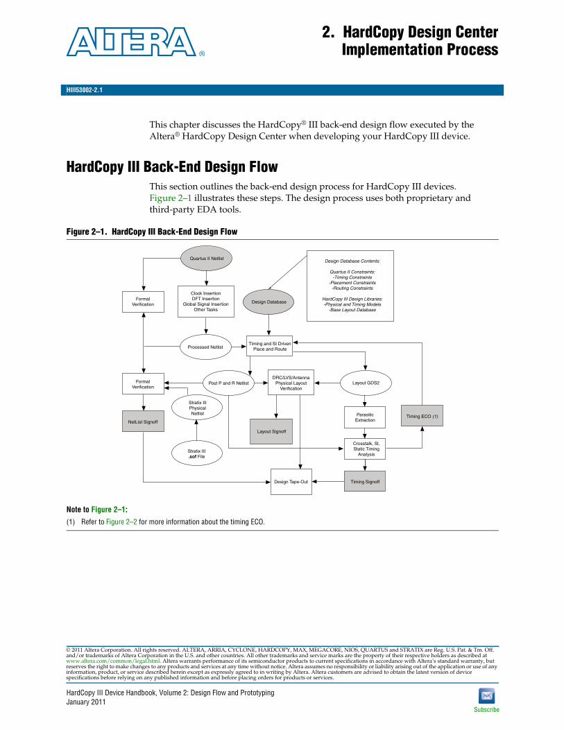
HardCopy III Device Handbook, Volume 2: Design FloJanuary 2011
HIII53002-2.1
© 2011 Altera Corporation. All rights reserved. ALTERA, ARRand/or trademarks of Altera Corporation in the U.S. and otherwww.altera.com/common/legal.html. Altera warrants performreserves the right to make changes to any products and servicesinformation, product, or service described herein except as expspecifications before relying on any published information and
January 2011HIII53002-2.1
2. HardCopy Design CenterImplementation Process
This chapter discusses the HardCopy® III back-end design flow executed by the Altera® HardCopy Design Center when developing your HardCopy III device.
HardCopy III Back-End Design FlowThis section outlines the back-end design process for HardCopy III devices. Figure 2–1 illustrates these steps. The design process uses both proprietary and third-party EDA tools.
Figure 2–1. HardCopy III Back-End Design Flow
Note to Figure 2–1:
(1) Refer to Figure 2–2 for more information about the timing ECO.
Quartus II Netlist
FormalVerification
Clock InsertionDFT Insertion
Global Signal InsertionOther Tasks
Design Database
Processed NetlistTiming and SI Driven
Place and Route
Design Database Contents:
Quartus II Constraints:-Timing Constraints
-Placement Constraints-Routing Constraints
HardCopy III Design Libraries:-Physical and Timing Models
-Base Layout Database
Post P and R NetlistFormalVerification
DRC/LVS/AntennaPhysical Layout
VerificationLayout GDS2
Layout Signoff
Design Tape-Out
NetList Signoff
Crosstalk, Sl,Static Timing
Analysis
Timing Signoff
ParasiticExtraction
Timing ECO (1)
Stratix IIIPhysicalNetlist
Stratix III.sof File
w and Prototyping
Subscribe
IA, CYCLONE, HARDCOPY, MAX, MEGACORE, NIOS, QUARTUS and STRATIX are Reg. U.S. Pat. & Tm. Off. countries. All other trademarks and service marks are the property of their respective holders as described at
ance of its semiconductor products to current specifications in accordance with Altera’s standard warranty, but at any time without notice. Altera assumes no responsibility or liability arising out of the application or use of any ressly agreed to in writing by Altera. Altera customers are advised to obtain the latest version of device before placing orders for products or services.
2–2 Chapter 2: HardCopy Design Center Implementation ProcessHardCopy III Back-End Design Flow
Design Netlist GenerationFor HardCopy III designs, the Quartus® II software generates a complete Verilog gate-level netlist of your design. The HardCopy Design Center uses the netlist to start the back-end process. In addition to the Verilog gate-level netlist, the Quartus II software generates information as part of the design database submitted by you to the Altera HardCopy Design Center. This information includes timing constraints, placement constraints, and global routing information. Generation of this database provides the HardCopy Design Center with the necessary information to complete the design of your HardCopy III device.
Design for TestabilityThe HardCopy Design Center inserts the necessary test structures into the HardCopy III Verilog netlist. These test structures include full-scan capable registers and scan chains, JTAG, and memory testing. After adding the test structures, the modified netlist is verified using third-party EDA formal verification software against the original Verilog netlist to ensure that the test structures have not broken your netlist functionality. “Formal Verification of the Processed Netlist” explains the formal verification process.
Clock Tree and Global Signal InsertionAlong with test insertion, the HardCopy Design Center adds a local layer of clock tree buffering to connect the global clock resources to the locally placed registers in the design. Global signals with high fan-out can also use dedicated global clock resources built into the base layers of all HardCopy III devices. The HardCopy Design Center does local buffering.
Tie-Off Connections for Unused ResourcesIf an unused resource in a customer design still exists in the HardCopy III database, the HardCopy Design Center uses special handling on the tie-off connections for these resources. I/O ports of unused resources are connected to power or ground so that the resources are in a lower power state. This is achieved by using the same metal layers that are used to configure and connect all resources used in the design.
Formal Verification of the Processed NetlistAfter all design-for-testability logic, clock tree buffering, global signal buffering, and tie-off connection are added to the processed netlist, the HardCopy Design Center uses third-party EDA formal verification software to compare the processed netlist with your submitted Verilog netlist generated by the Quartus II software. Added test structures are constrained to bypass mode during formal verification to verify that your design’s intended functionality is unchanged.
HardCopy III Device Handbook, Volume 2: Design Flow and Prototyping January 2011 Altera Corporation
Chapter 2: HardCopy Design Center Implementation Process 2–3HardCopy III Back-End Design Flow
Timing and Signal Integrity Driven Place and RoutePlacement and global signal routing is principally done in the Quartus II software before submitting the HardCopy III design to the HardCopy Design Center. With the Quartus II software, you control the placement and timing driven placement optimization of your design. The Quartus II software also does global routing of your signal nets, and passes this information in the design database to the HardCopy Design Center to do the final routing. After the design is submitted, Altera engineers use the placement and global routing information provided in the design database to do final routing and timing closure, and to perform signal integrity and crosstalk analysis. This may require buffer and delay cell insertion in the design through an engineering change order (ECO). The resulting post place and route netlist is verified again with the source netlist and the processed netlist to guarantee that functionality was not altered in the process. For more details about back-end timing closure and timing ECOs, refer to “Back-End Timing Closure” and “Timing ECOs”.
Parasitic Extraction and Timing AnalysisAfter the HardCopy Design Center places and routes your design, a .gds2 design file is generated. Parasitic extraction uses the physical layout of the design stored in the database to extract the resistance and capacitance values for all signal nets in the design. The HardCopy Design Center uses these parasitic values to calculate the path delays through the design for static timing analysis and crosstalk analysis.
Back-End Timing ClosureThe Quartus II software provides a pre-layout estimation of your HardCopy III design performance. The Altera HardCopy Design Center then uses industry leading EDA software to complete the back-end layout and extract the final timing results prior to tape-out. Altera performs rigorous timing analysis on the HardCopy III design during its back-end implementation, ensuring that it meets the required timing constraints. After generating the customized metal interconnect for the HardCopy III device, Altera checks the design timing with a static timing analysis tool. The static timing analysis tool may report timing violations, which are reviewed with the customer.
The critical timing paths of the HardCopy III device may be different from the corresponding paths in the Stratix III FPGA revision; these differences can exist for several reasons. While maintaining the same set of features as the corresponding Stratix III FPGA, HardCopy III devices have a highly optimized die size to make them as small as possible. Because of the customized interconnect structure that makes this optimization possible, the delay through each signal path is different from the original Stratix III FPGA design. Therefore, it is important to constrain the Stratix III FPGA and HardCopy III devices to the exact, system-level timing requirements that need to be achieved. Timing violations seen in the Quartus II project or in the HardCopy Design Center back-end process must be fixed or waived prior to the design tape-out.
Timing ECOsIn an ASIC design, small incremental changes to a design database are termed ECOs. In the HardCopy III design flow, timing closure ECOs are performed by Altera’s HardCopy Design Center after the initial post-layout timing data is available.
January 2011 Altera Corporation HardCopy III Device Handbook, Volume 2: Design Flow and Prototyping

2–4 Chapter 2: HardCopy Design Center Implementation ProcessHardCopy III Back-End Design Flow
The Altera HardCopy Design Center runs static timing analysis on the design. This analysis may show that the place and route tool was not able to close timing automatically on some paths. The HardCopy Design Center engineer will determine the best way to fix the timing on these paths (for example, by adding delay cells to fix a hold time violation). This list of changes is fed back into the place and route tool which subsequently implements the changes. The impact to the place and route database is minimized by maintaining all of the pre-existing placement and routing, and only changing the paths that need improvement.
The parasitic resistances and capacitances of the customized interconnect are extracted, and are used in conjunction with the static timing analysis tool to re-check the timing of the design. Detected crosstalk violations on signals are fixed by adding additional buffering to increase the setup or hold margin on victim signals. In-line buffering and small buffer tree insertion is done for signals with high fan-out, high transition times, or high capacitive loading. Figure 2–2 shows this flow in more detail.
The back-end flow produces the final signoff timing for your HardCopy III device. The Quartus II software produces the timing report for HardCopy III based on global routing and does not factor in the exact physical parasitic of the routed nets. The Quartus II software also does not factor in the crosstalk effect that neighboring nets can have on interconnect capacitance.
Figure 2–2. Timing Closure ECO Flow Diagram
Timing Closure ECO Iterations
ECO FilePreparation
Merge New Cells into Physical
Database
Placement
Clock Tree Synthesisand High Fan-out
Net Buffering
Detailed Routing
Static Timing Analysis
TimingViolations
Timing ClosedDatabase
HardCopy III Device Handbook, Volume 2: Design Flow and Prototyping January 2011 Altera Corporation

Chapter 2: HardCopy Design Center Implementation Process 2–5Conclusion
Formal Verification of the Post-Layout NetlistIn addition to the .gds2 file and parasitic files that are generated by the HardCopy Design Center, the post-layout netlist is also generated for formal verification with Stratix III FPGAs. The HardCopy Design Center checks the functional equivalence between the Stratix III FPGA prototype and HardCopy III device according to the Stratix III .sof file and HardCopy III post-layout netlist.
Layout VerificationWhen the Timing Analysis reports that all timing requirements are met, the design layout goes into the final stage of verification for manufacturability. The HardCopy Design Center performs physical Design Rule Checking (DRC), antenna checking of long traces of signals in the layout, and a comparison of layout to the design netlist, commonly referred to as Layout Versus Schematic (LVS). These tasks guarantee that the layout contains the exact logic represented in the place-and-route netlist and the physical layout.
Design SignoffThe Altera HardCopy III back-end design methodology has a thorough verification and signoff process, guaranteeing your design’s functionality. Signoff occurs after completing the final place-and-route netlist functional verification, layout verification for manufacturability, and timing analysis. After achieving all three signoff points, Altera begins the manufacturing of the HardCopy III devices.
ConclusionAltera’s back-end design methodology ensures that your design converts successfully from your Stratix III FPGA prototype to the HardCopy III ASIC. Altera’s unique system development methodology offers an excellent way for you to benefit from using a Stratix III FPGA for design prototyping and debugging, and using a HardCopy III ASIC for volume production.
Document Revision HistoryTable 2–1 shows the revision history for this document.
Table 2–1. Document Revision History
Date Version Changes
January 2011 2.1 Minor text edits.
December 2008 2.0■ Minor text edits.
■ Chapter listed as p/n 52001 in ADoQS for this version release.
May 2008 1.0 Initial release.
January 2011 Altera Corporation HardCopy III Device Handbook, Volume 2: Design Flow and Prototyping

2–6 Chapter 2: HardCopy Design Center Implementation ProcessDocument Revision History
HardCopy III Device Handbook, Volume 2: Design Flow and Prototyping January 2011 Altera Corporation

HardCopy III Device Handbook, Volume 2: Design FloMarch 2012
HIII53003-3.3
© 2012 Altera Corporation. All rights reserved. ALTERA, ARRand/or trademarks of Altera Corporation in the U.S. and otherwww.altera.com/common/legal.html. Altera warrants performreserves the right to make changes to any products and servicesinformation, product, or service described herein except as expspecifications before relying on any published information and
March 2012HIII53003-3.3
3. Mapping Stratix III Device Resourcesto HardCopy III Devices
This chapter discusses the available options for mapping from a Stratix® III device to a HardCopy® III device.
The Quartus II software limits resources to those available to both the Stratix III FPGA and the HardCopy III ASIC. It also ensures that the design revision targeting a HardCopy III device retains the same functionality as the original Stratix III design.
When compiling designs with the Quartus II software, you can specify one HardCopy III target device and one or more Stratix III mapping devices. When you specify at least one mapping device, the Quartus II compiler constrains I/O pins and relevant hard IP blocks to the minimum resources available in any of the selected mapping devices. This feature allows vertical mapping between devices using the same package footprint.
Selecting a HardCopy III device as a companion device is similar to adding another Stratix III device to the mapping device chain. The Quartus II software compiles the design to use the common resources available in all of the selected Stratix III and HardCopy III devices.
The HardCopy III companion device becomes the target device when you create the HardCopy companion revision.
w and Prototyping
Subscribe
IA, CYCLONE, HARDCOPY, MAX, MEGACORE, NIOS, QUARTUS and STRATIX are Reg. U.S. Pat. & Tm. Off. countries. All other trademarks and service marks are the property of their respective holders as described at
ance of its semiconductor products to current specifications in accordance with Altera’s standard warranty, but at any time without notice. Altera assumes no responsibility or liability arising out of the application or use of any ressly agreed to in writing by Altera. Altera customers are advised to obtain the latest version of device before placing orders for products or services.

3–2 Chapter 3: Mapping Stratix III Device Resources to HardCopy III Devices
Figure 3–1 shows the Device page of the Settings dialog box, where you choose the companion device for the target device selected. The Device panel lists appropriate companion devices based on the target device you select.
When you select a HardCopy III companion device, the Quartus II software fits your design to common resources in the I/Os, clock structures, PLLs, memory blocks, and core logic for digital signal processing (DSP).
f For more information about compiling with Stratix III and HardCopy III companion revisions using the Quartus II software, refer to the Quartus II Support for HardCopy Series Devices chapter in volume 1 of the Quartus II Handbook.
Figure 3–1. Quartus II Device Settings Page with HardCopy III Device Selected as Companion Device
HardCopy III Device Handbook, Volume 2: Design Flow and Prototyping March 2012 Altera Corporation

Chapter 3: Mapping Stratix III Device Resources to HardCopy III Devices 3–3HardCopy III and Stratix III Mapping Options
HardCopy III and Stratix III Mapping Options HardCopy III ASICs offer a wide range of family options that can map with various Stratix III FPGAs.
Table 3–1 lists the available HardCopy III and Stratix III companion pairs.
Table 3–1. HardCopy III and Stratix III Companion Devices (Part 1 of 2)
Companion PairHardCopy III Packages
HardCopy III ASICs Stratix III FPGA Prototypes
HC325WF484N
EP3SL110--F780 (1)
484-pin FineLine BGA - Wire Bond
EP3SL150--F780 (1)
EP3SE110--F780 (1)
EP3SL200--H780 (1)
EP3SE260--H780 (1)
EP3SL340--H1152 (2)
HC325FF484N
EP3SL110--F780
484-pin FineLine BGA
EP3SL150--F780
EP3SE110--F780
EP3SL200--H780
EP3SE260--H780
EP3SL340--H1152 (2)
HC325WF780N
EP3SL110--F780
780-pin FineLine BGA - Wire Bond
EP3SL150--F780
EP3SE110--F780
EP3SL200--H780
EP3SE260--H780
EP3SL340--H1152 (2)
HC325FF780N
EP3SL110--F780
780-pin FineLine BGA
EP3SL150--F780
EP3SE110--F780
EP3SL200--H780
EP3SE260--H780
EP3SL340--H1152
HC335LF1152N
EP3SL150--F1152
1152-pin FineLine BGA
EP3SE110--F1152
EP3SL200--F1152
EP3SE260--F1152
EP3SL340--H1152
March 2012 Altera Corporation HardCopy III Device Handbook, Volume 2: Design Flow and Prototyping

3–4 Chapter 3: Mapping Stratix III Device Resources to HardCopy III DevicesHardCopy III and Stratix III Mapping Options
When the Quartus II software successfully compiles a design, the HardCopy Device Resource Guide in the Fitter Compilation Report contains information about mapping compatibility to a HardCopy III device. Use this information to select the optimal HardCopy III device for the prototype Stratix III device based on resource and package requirements.
Table 3–2 shows the available resources for prototyping on a Stratix III device when choosing a HardCopy III device.
HC335FF1152N
EP3SL150--F1152
1152-pin FineLine BGA
EP3SE110--F1152
EP3SL200--F1152
EP3SE260--F1152
EP3SL340--H1152
HC335LF1517N
EP3SL200--F1517
1517-pin FineLine BGAEP3SE260--F1517
EP3SL340--F1517
HC335FF1517N
EP3SL200--F1517
1517-pin FineLine BGAEP3SE260--F1517
EP3SL340--F1517
Notes to Table 3–1:
(1) This mapping is a non-socket replacement path that requires a different board design for the Stratix III device and the HardCopy III device. The Stratix III device is in a 780-pin FBGA package, while the HardCopy III device is in a 484-pin FBGA package.
(2) This mapping is a non-socket replacement path that requires a different board design for the Stratix III device and the HardCopy III device. The Stratix III device is in a 1152-pin FBGA package, while the HardCopy III device is in a 484-pin FBGA package.
Table 3–1. HardCopy III and Stratix III Companion Devices (Part 2 of 2)
Companion PairHardCopy III Packages
HardCopy III ASICs Stratix III FPGA Prototypes
Table 3–2. HardCopy III ASIC Features (Part 1 of 2)
HardCopy III ASIC
Stratix III FPGA
Prototype
ASIC Equivalent Gates (1)
M9K Blocks
M144K Blocks
Total Dedicated RAM Bits (not
including MLABs) (2)
18 x 18 - Bit Multipliers (FIR Mode)
PLLs
HC325
EP3SL110 2.7 M 275 12 4,203 Kb 288 4
EP3SL150 3.6 M 355 16 5,499 Kb 384 4
EP3SE110 5.8 M 639 16 8,055 Kb 896 4
EP3SL200 5.3 M 468 32 8,820 Kb 576 4
EP3SE260 6.9 M 864 32 12,384 Kb 768 4
EP3SL340 7.0 M 864 32 12,384 Kb 576 4
HardCopy III Device Handbook, Volume 2: Design Flow and Prototyping March 2012 Altera Corporation
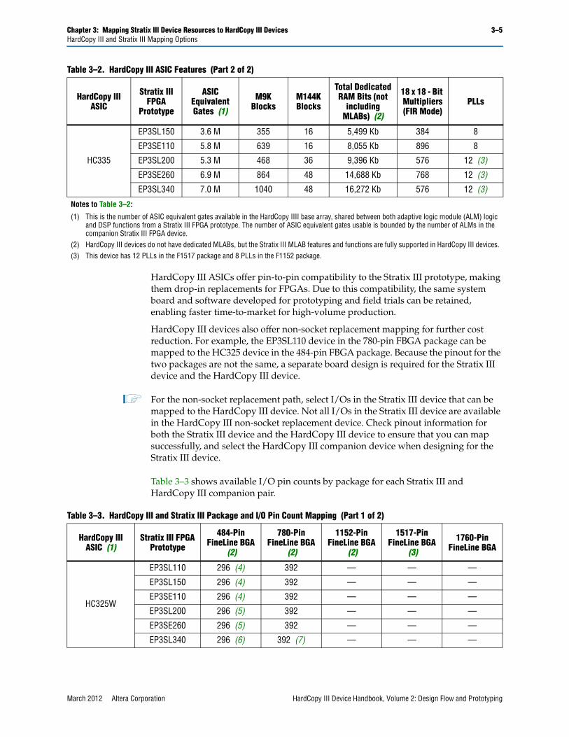
Chapter 3: Mapping Stratix III Device Resources to HardCopy III Devices 3–5HardCopy III and Stratix III Mapping Options
HardCopy III ASICs offer pin-to-pin compatibility to the Stratix III prototype, making them drop-in replacements for FPGAs. Due to this compatibility, the same system board and software developed for prototyping and field trials can be retained, enabling faster time-to-market for high-volume production.
HardCopy III devices also offer non-socket replacement mapping for further cost reduction. For example, the EP3SL110 device in the 780-pin FBGA package can be mapped to the HC325 device in the 484-pin FBGA package. Because the pinout for the two packages are not the same, a separate board design is required for the Stratix III device and the HardCopy III device.
1 For the non-socket replacement path, select I/Os in the Stratix III device that can be mapped to the HardCopy III device. Not all I/Os in the Stratix III device are available in the HardCopy III non-socket replacement device. Check pinout information for both the Stratix III device and the HardCopy III device to ensure that you can map successfully, and select the HardCopy III companion device when designing for the Stratix III device.
Table 3–3 shows available I/O pin counts by package for each Stratix III and HardCopy III companion pair.
HC335
EP3SL150 3.6 M 355 16 5,499 Kb 384 8
EP3SE110 5.8 M 639 16 8,055 Kb 896 8
EP3SL200 5.3 M 468 36 9,396 Kb 576 12 (3)
EP3SE260 6.9 M 864 48 14,688 Kb 768 12 (3)
EP3SL340 7.0 M 1040 48 16,272 Kb 576 12 (3)
Notes to Table 3–2:
(1) This is the number of ASIC equivalent gates available in the HardCopy IIII base array, shared between both adaptive logic module (ALM) logic and DSP functions from a Stratix III FPGA prototype. The number of ASIC equivalent gates usable is bounded by the number of ALMs in the companion Stratix III FPGA device.
(2) HardCopy III devices do not have dedicated MLABs, but the Stratix III MLAB features and functions are fully supported in HardCopy III devices.(3) This device has 12 PLLs in the F1517 package and 8 PLLs in the F1152 package.
Table 3–2. HardCopy III ASIC Features (Part 2 of 2)
HardCopy III ASIC
Stratix III FPGA
Prototype
ASIC Equivalent Gates (1)
M9K Blocks
M144K Blocks
Total Dedicated RAM Bits (not
including MLABs) (2)
18 x 18 - Bit Multipliers (FIR Mode)
PLLs
Table 3–3. HardCopy III and Stratix III Package and I/O Pin Count Mapping (Part 1 of 2)
HardCopy III ASIC (1)
Stratix III FPGA Prototype
484-Pin FineLine BGA
(2)
780-Pin FineLine BGA
(2)
1152-Pin FineLine BGA
(2)
1517-Pin FineLine BGA
(3)
1760-Pin FineLine BGA
HC325W
EP3SL110 296 (4) 392 — — —
EP3SL150 296 (4) 392 — — —
EP3SE110 296 (4) 392 — — —
EP3SL200 296 (5) 392 — — —
EP3SE260 296 (5) 392 — — —
EP3SL340 296 (6) 392 (7) — — —
March 2012 Altera Corporation HardCopy III Device Handbook, Volume 2: Design Flow and Prototyping

3–6 Chapter 3: Mapping Stratix III Device Resources to HardCopy III DevicesSummary of Differences Between HardCopy III and Stratix III Devices
Summary of Differences Between HardCopy III and Stratix III DevicesHardCopy III ASICs are functionally equivalent to Stratix III FPGAs, but they have architectural differences. When implementing your design and laying out your board, consider these differences to ensure successful design mapping from the Stratix III FPGA to the HardCopy III ASIC.
Architecture differences between the Stratix III FPGA and the HardCopy III ASIC include:
■ Maximum core voltage is 0.9 V in HardCopy III devices compared with selectable core voltages of 0.9 V or 1.1 V in Stratix III devices.
■ Maximum VCCIO power supply of 3.0 V.
HC325F
EP3SL110 296 (4) 488 — — —
EP3SL150 296 (4) 488 — — —
EP3SE110 296 (4) 488 — — —
EP3SL200 296 (5) 488 — — —
EP3SE260 296 (5) 488 — — —
EP3SL340 296 (6) 488 (7) — — —
HC335L
EP3SL150 — — 744 — —
EP3SE110 — — 744 — —
EP3SL200 — — 744 880 —
EP3SE260 — — 744 880 —
EP3SL340 — — 744 880 —
HC335F
EP3SL150 — — 744 — —
EP3SE110 — — 744 — —
EP3SL200 — — 744 880 —
EP3SE260 — — 744 880 —
EP3SL340 — — 744 880 —
Notes to Table 3–3:
(1) The last letter in the HardCopy III device name refers to the following package types: F–Performance-optimized flip-chip package, L–Cost-optimized flip-chip package, W–Low-cost wirebond package.
(2) All I/O pin counts include eight dedicated clock inputs (CLK1p, CLK1n, CLK3p, CLK3n, CLK8p, CLK8n, CLK10p, and CLK10n) that can be used for data inputs.
(3) All I/O pin counts include eight dedicated clock inputs (CLK1p, CLK1n, CLK3p, CLK3n, CLK8p, CLK8n, CLK10p and CLK10n) and eight dedicated corner PLL clock inputs (PLL_L1_CLKp, PLL_L1_CLKn, PLL_L4_CLKp, PLL_L4_CLKn, PLL_R4_CLKp, PLL_R4_CLKn, PLL_R1_CLKp, and PLL_R1_CLKn) that can be used for data inputs.
(4) This mapping is a non-socket replacement path and requires a different board design for the Stratix III device and the HardCopy III device. The Stratix III device is in a 780-Pin FineLine BGA package while the HardCopy III device is in a 484-Pin FineLine BGA package.
(5) This mapping is a non-socket replacement path and requires a different board design for the Stratix III device and the HardCopy III device. The Stratix III device is in a 780-Pin Hybrid FineLine BGA package while the HardCopy III device is in a 484-Pin FineLine BGA package.
(6) This mapping is a non-socket replacement path and requires a different board design for the Stratix III device and the HardCopy III device. The Stratix III device is in a 1152-Pin Hybrid FineLine BGA package while the HardCopy III device is in a 484-Pin FineLine BGA package.
(7) This mapping is a non-socket replacement path and requires a different board design for the Stratix III device and the HardCopy III device. The Stratix III device is in a 1152-Pin Hybrid FineLine BGA package while the HardCopy III device is in a 780-Pin FineLine BGA package.
Table 3–3. HardCopy III and Stratix III Package and I/O Pin Count Mapping (Part 2 of 2)
HardCopy III ASIC (1)
Stratix III FPGA Prototype
484-Pin FineLine BGA
(2)
780-Pin FineLine BGA
(2)
1152-Pin FineLine BGA
(2)
1517-Pin FineLine BGA
(3)
1760-Pin FineLine BGA
HardCopy III Device Handbook, Volume 2: Design Flow and Prototyping March 2012 Altera Corporation

Chapter 3: Mapping Stratix III Device Resources to HardCopy III Devices 3–7Designing with HardCopy III Core Supply Requirements
■ HardCopy III inputs tolerate 3.3 V levels, but you might have to use external clamping diodes on the board to keep the pins operating within specification.
■ HardCopy III devices have up to 20 I/O banks and 880 I/O pins, while the largest Stratix III companion devices have up to 24 I/O banks and 976 I/O pins on a 1517-pin FPGA.
■ The number of global and regional clocks is identical for Stratix III and HardCopy III devices, but Stratix III devices have up to 116 peripheral clocks, while HardCopy III devices have up to 88. The Quartus II software limits the clock availability on Stratix III and HardCopy III companion pairs to ensure device mapping.
■ Configuration is not required for HardCopy III devices; therefore, these Stratix III features are not supported:
■ Programming modes and features such as remote update and .pof encryption.
■ Cyclical redundancy check (CRC) for configuration error detection.
■ 256-bit (AES) volatile and non-volatile security key to protect designs.
■ JTAG instructions used for configuration.
■ FPGA configuration emulation mode.
■ Boundary scan (BSCAN) chain length is different and varies with device density.
■ Memory Initialization Files (.mif) for embedded memories used as RAM are not supported.
■ Stratix III LAB/MLAB and DSP functions are implemented with HCells in HardCopy III devices instead of dedicated blocks.
■ Stratix III Programmable Power Technology is not supported in HardCopy III devices. However, HardCopy III ASIC architecture offers performance on par with Stratix III devices with significantly lower power.
Designing with HardCopy III Core Supply RequirementsAltera HardCopy III ASICs are manufactured with a more advanced process technology than Stratix III FPGAs. Each technology is centered on a unique core voltage requirement. HardCopy III nominal core voltage is centered at 0.9 V, whereas Stratix III devices use a typical voltage of 1.1 V. Due to the unique voltage requirements of each device family, design your board’s power plane and supply to support both Stratix III and HardCopy III devices to minimize changes required when moving from Stratix III prototyping to HardCopy III devices. A number of power supply regulator manufacturers account for this requirement and require only a few components to be substituted to change the power supply level of the board.
f For more information about designing power supply methods to account for Stratix III and HardCopy III core supply differences, refer to the Power Supply and Temperature Sensing Diode in HardCopy III Devices chapter in volume 1 of the HardCopy III Device Handbook.
March 2012 Altera Corporation HardCopy III Device Handbook, Volume 2: Design Flow and Prototyping

3–8 Chapter 3: Mapping Stratix III Device Resources to HardCopy III DevicesDesigning with HardCopy III I/Os
Designing with HardCopy III I/OsHardCopy III ASICs support a wide range of industry I/O standards that match Stratix III supported standards. The exception is that HardCopy III I/O standards support a VCCIO voltage range from 1.2 to 3.0 V. A VCCIO of 3.3 V is not supported by HardCopy III I/O banks. For more information about this topic, refer to “Mapping HardCopy III and Stratix III I/Os and Modular I/O Banks” on page 3–8.
Aside from the VCCIO requirement, HardCopy III I/O standards support the same specifications as their Stratix III companion equivalent. The I/O arrangement in HardCopy III devices matches the I/O arrangement in Stratix III devices such that I/O pins located on the left and right side I/O banks contain circuits dedicated to high-speed differential I/O interfaces, but have the ability to support external memory devices if required. The top and bottom I/O banks contain dedicated circuitry to optimize external memory interfaces. They also have the ability to support high-speed differential inputs and outputs at lesser speeds than the left and right side banks.
1 When you select a HardCopy III companion device to compile with your Stratix III target device (and vice versa), the Quartus II software ensures that I/O pins and I/O assignments are compatible with all selected devices.
f For more information, refer to the HardCopy III Device I/O Features chapter in volume 1 of the HardCopy III Device Handbook.
Mapping HardCopy III and Stratix III I/Os and Modular I/O Banks I/O pins in Stratix III and HardCopy III devices are arranged in groups called modular I/O banks. On Stratix III devices, the number of I/O banks can range from 16 to 24 banks. On HardCopy III devices, the number of I/O banks can range from 12 to 20 banks.
In both Stratix III and HardCopy III devices, the maximum number of I/O banks per side is four or six, depending on the device density. When migrating between devices with a different number of I/O banks per side, the middle or “B” bank is removed or inserted. For example, when moving from a 24-bank Stratix III device to a 16-bank Stratix III or HardCopy III device, the banks that are dropped are “B” banks, namely 1B, 2B, 3B, 4B, 5B, 6B, 7B, and 8B.
HardCopy III devices do not have banks 1B, 2B, 5B, and 6B. When you design with a Stratix III device that has 24 banks, the Quartus II software limits the available banks common to all devices selected if a HardCopy III device is selected as a companion pair. If you try to assign I/O pins to a non-existent bank in a mapping or companion device, the Quartus II compilation halts with an error.
The following are examples of Quartus II compilation errors:
Error: I/O pins (xx) assigned in I/O bank 1B. The I/O bank does not exist in the selected device
Error: Device migration enabled -- compilation may have failed due to additional constraints when migrating
Error: Can't fit design in device
HardCopy III Device Handbook, Volume 2: Design Flow and Prototyping March 2012 Altera Corporation
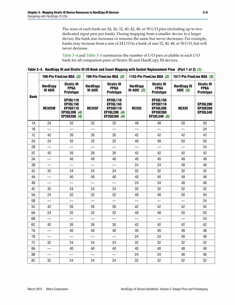
Chapter 3: Mapping Stratix III Device Resources to HardCopy III Devices 3–9Designing with HardCopy III I/Os
)
The sizes of each bank are 24, 26, 32, 40, 42, 48, or 50 I/O pins (including up to two dedicated input pins per bank). During mapping from a smaller device to a larger device, the bank size increases or remains the same but never decreases. For example, banks may increase from a size of 24 I/O to a bank of size 32, 40, 48, or 50 I/O, but will never decrease.
Table 3–4 and Table 3–5 summarize the number of I/O pins available in each I/O bank for all companion pairs of Stratix III and HardCopy III devices.
Table 3–4. HardCopy III and Stratix III I/O Bank and Count Mapping with Socket Replacement Flow (Part 1 of 2) (1)
Bank
780-Pin FineLine BGA (2) 780-Pin FineLine BGA (2) 1152-Pin FineLine BGA (2) 1517-Pin FineLine BGA (3
HardCopy III ASIC
Stratix III FPGA
Prototype
HardCopy III ASIC
Stratix III FPGA
Prototype
HardCopy III ASIC (2)
Stratix III FPGA
Prototype
HardCopy III ASIC (3)
Stratix IIIFPGA
Prototype
HC325W
EP3SL110EP3SL150EP3SE110
EP3SL200 (4)EP3SE260 (4)
HC325F
EP3SL110EP3SL150EP3SE110
EP3SL200 (4)EP3SE260 (4)
HC335
EP3SL150EP3SE110EP3SL200EP3SE260
EP3SL340 (5)
HC335EP3SL200EP3SE260EP3SL340
1A 24 32 32 32 48 48 50 50
1B — — — — — — — 24
1C 42 26 26 26 42 42 42 42
2A 24 32 32 32 48 48 50 50
2B — — — — — — — 24
2C 42 26 26 26 42 42 42 42
3A — 40 40 40 40 40 48 48
3B — — — — 24 24 48 48
3C 32 24 24 24 32 32 32 32
4A — 40 40 40 40 40 48 48
4B — — — — 24 24 48 48
4C 32 24 24 24 32 32 32 32
5A 24 32 32 32 48 48 50 50
5B — — — — — — — 24
5C 42 26 26 26 42 42 42 42
6A 24 32 32 32 48 48 50 50
6B — — — — — — — 24
6C 42 26 26 26 42 42 42 42
7A — 40 40 40 40 40 48 48
7B — — — — 24 24 48 48
7C 32 24 24 24 32 32 32 32
8A — 40 40 40 40 40 48 48
8B — — — — 24 24 48 48
8C 32 24 24 24 32 32 32 32
March 2012 Altera Corporation HardCopy III Device Handbook, Volume 2: Design Flow and Prototyping

3–10 Chapter 3: Mapping Stratix III Device Resources to HardCopy III DevicesDesigning with HardCopy III I/Os
)
Total I/O 392 488 488 488 744 744 880 976
Notes to Table 3–4:
(1) User I/O pin counts are preliminary.(2) All I/O pin counts include eight dedicated clock inputs (CLK1p, CLK1n, CLK3p, CLK3n, CLK8p, CLK8n, CLK10p and CLK10n) that can be used for
data inputs.(3) All I/O pin counts include eight dedicated clock inputs (CLK1p, CLK1n, CLK3p, CLK3n, CLK8p, CLK8n, CLK10p and CLK10n) and eight dedicated
corner PLL clock inputs (PLL_L1_CLKp, PLL_L1_CLKn, PLL_L4_CLKp, PLL_L4_CLKn, PLL_R4_CLKp, PLL_R4_CLKn, PLL_R1_CLKp, and PLL_R1_CLKn) that can be used for data inputs.
(4) The EP3SE260 and EP3SL200 FPGAs are offered only in the H780 package.(5) The EP3SL340 FPGA is offered only in the H1152 package.
Table 3–4. HardCopy III and Stratix III I/O Bank and Count Mapping with Socket Replacement Flow (Part 2 of 2) (1)
Bank
780-Pin FineLine BGA (2) 780-Pin FineLine BGA (2) 1152-Pin FineLine BGA (2) 1517-Pin FineLine BGA (3
HardCopy III ASIC
Stratix III FPGA
Prototype
HardCopy III ASIC
Stratix III FPGA
Prototype
HardCopy III ASIC (2)
Stratix III FPGA
Prototype
HardCopy III ASIC (3)
Stratix IIIFPGA
Prototype
HC325W
EP3SL110EP3SL150EP3SE110
EP3SL200 (4)EP3SE260 (4)
HC325F
EP3SL110EP3SL150EP3SE110
EP3SL200 (4)EP3SE260 (4)
HC335
EP3SL150EP3SE110EP3SL200EP3SE260
EP3SL340 (5)
HC335EP3SL200EP3SE260EP3SL340
HardCopy III Device Handbook, Volume 2: Design Flow and Prototyping March 2012 Altera Corporation

Chapter 3:M
apping Stratix III Device Resources to HardCopy III Devices3–11
Designing with HardCopy III I/Os
March 2012
Altera CorporationHardCopy III Device Handbook, Volum
e 2: Design Flow and Prototyping
and cost. Because HardCopy III and the HardCopy III device. Table 3–5 on-socket replacement flow.
f 2)
in BGA
780-Pin FineLine BGA
1152-pin FineLine BGA
III pe
HardCopy III ASICStratix III
FPGA Prototype
40 HC325F EP3SL340
32 48
— —
26 42
32 48
— —
26 42
40 40
— 24
24 32
40 40
— 24
24 32
32 48
— —
26 42
32 48
— —
HardCopy III ASICs offer the non-socket replacement flow to reduce design board spaceStratix III device packages are different, some Stratix III device I/Os are not available in shows the number of I/Os of each bank on Stratix III and HardCopy III devices for the n
Table 3–5. HardCopy III and Stratix III I/O Bank and Count Mapping with Non-Socket Replacement Flow (Note 1) (Part 1 o
Bank
484-pin FineLine BGA
780-Pin FineLine BGA
484-pin FineLine BGA
1152-pin FineLine BGA
780-Pin FineLine BGA
1152-pFineLine
HardCopy III ASIC Stratix III FPGA Prototype HardCopy III ASIC Stratix III FPGA
Prototype HardCopy III ASICStratix
FPGAPrototy
HC325WHC325F
EP3SL110EP3SL150EP3SE110EP3SL200EP3SE260
HC325WHC325F EP3SL340 HC325W EP3SL3
1A 24 32 24 48 24 48
1B — — — — — —
1C 26 26 26 42 42 42
2A 24 32 24 48 24 48
2B — — — — — —
2C 26 26 26 42 42 42
3A — 40 — 40 — 40
3B — — — 24 — 24
3C 24 24 24 32 32 32
4A — 40 — 40 — 40
4B — — — 24 — 24
4C 24 24 24 32 32 32
5A 24 32 24 48 24 48
5B — — — — — —
5C 26 26 26 42 42 42
6A 24 32 24 48 24 48
6B — — — — — —
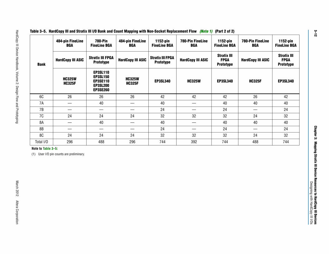
3–12Chapter 3:
Mapping Stratix III Device Resources to HardCopy III Devices
Designing with HardCopy III I/Os
HardCopy III Device Handbook, Volume 2: Design Flow
and PrototypingM
arch 2012 Altera Corporation
26 42
40 40
— 24
24 32
40 40
— 24
24 32
488 744
f 2)
in BGA
780-Pin FineLine BGA
1152-pin FineLine BGA
III pe
HardCopy III ASICStratix III
FPGA Prototype
40 HC325F EP3SL340
6C 26 26 26 42 42 42
7A — 40 — 40 — 40
7B — — — 24 — 24
7C 24 24 24 32 32 32
8A — 40 — 40 — 40
8B — — — 24 — 24
8C 24 24 24 32 32 32
Total I/O 296 488 296 744 392 744
Note to Table 3–5:
(1) User I/O pin counts are preliminary.
Table 3–5. HardCopy III and Stratix III I/O Bank and Count Mapping with Non-Socket Replacement Flow (Note 1) (Part 2 o
Bank
484-pin FineLine BGA
780-Pin FineLine BGA
484-pin FineLine BGA
1152-pin FineLine BGA
780-Pin FineLine BGA
1152-pFineLine
HardCopy III ASIC Stratix III FPGA Prototype HardCopy III ASIC Stratix III FPGA
Prototype HardCopy III ASICStratix
FPGAPrototy
HC325WHC325F
EP3SL110EP3SL150EP3SE110EP3SL200EP3SE260
HC325WHC325F EP3SL340 HC325W EP3SL3

Chapter 3: Mapping Stratix III Device Resources to HardCopy III Devices 3–13Designing with HardCopy III I/Os
HardCopy III Supported I/O StandardsHardCopy III ASICs support the same I/O standards as Stratix III FPGAs, except 3.3 V LVTTL/LVCMOS I/O standards.
Table 3–6 lists I/O standards that HardCopy III devices support.
Table 3–6. HardCopy III I/O Standards and Voltage Levels (Part 1 of 2) (Note 1)
I/O Standard Standard Support
VCCIO (V) VCCPD (V)
(Pre-Driver
Voltage)
VREF (V) (Input Ref Voltage)
VTT (V) (Board Termination
Voltage)
Input Operation Output Operation
Column I/O
Banks
RowI/O
Banks
Column I/O
Banks
RowI/O
Banks
3.0-V LVTTL (1) JESD8-B 3.0/2.5 3.0/2.5 3.0 3.0 3.0 — —
3.0-V LVCMOS (1) JESD8-B 3.0/2.5 3.0/2.5 3.0 3.0 3.0 — —
2.5-V LVTTL/LVCMOS JESD8-5 3.0/2.5 3.0/2.5 2.5 2.5 2.5 — —
1.8-V LVTTL/LVCMOS JESD8-7 1.8/1.5 1.8/1.5 1.8 1.8 2.5 — —
1.5-V LVTTL/LVCMOS JESD8-11 1.8/1.5 1.8/1.5 1.5 1.5 2.5 — —
1.2-V LVTTL/LVCMOS JESD8-12 1.2 1.2 1.2 1.2 2.5 — —
3.0-V PCI (4) PCI Rev 2.1 3.0 3.0 3.0 3.0 3.0 — —
3.0-V PCI-X (4) PCI-X Rev 1.0 3.0 3.0 3.0 3.0 3.0 — —
SSTL-2 Class I JESD8-9B (2) (2) 2.5 2.5 2.5 1.25 1.25
SSTL-2 Class II JESD8-9B (2) (2) 2.5 2.5 2.5 1.25 1.25
SSTL-18 Class I JESD8-15 (2) (2) 1.8 1.8 2.5 0.90 0.90
SSTL-18 Class II JESD8-15 (2) (2) 1.8 1.8 2.5 0.90 0.90
SSTL-15 Class I — (2) (2) 1.5 1.5 2.5 0.75 0.75
SSTL-15 Class II (3) — (2) (2) 1.5 N/A 2.5 0.75 0.75
HSTL-18 Class I JESD8-6 (2) (2) 1.8 1.8 2.5 0.90 0.90
HSTL-18 Class II JESD8-6 (2) (2) 1.8 1.8 2.5 0.90 0.90
HSTL-15 Class I JESD8-6 (2) (2) 1.5 1.5 2.5 0.75 0.75
HSTL-15 Class II (3) JESD8-6 (2) (2) 1.5 N/A 2.5 0.75 0.75
HSTL-12 Class I JESD8-16A (2) (2) 1.2 1.2 2.5 0.6 0.6
HSTL-12 Class II (3) JESD8-16A (2) (2) 1.2 N/A 2.5 0.6 0.6
Differential SSTL-2 Class I JESD8-9B (2) (2) 2.5 2.5 2.5 — 1.25
Differential SSTL-2 Class II JESD8-9B (2) (2) 2.5 2.5 2.5 — 1.25
March 2012 Altera Corporation HardCopy III Device Handbook, Volume 2: Design Flow and Prototyping

3–14 Chapter 3: Mapping Stratix III Device Resources to HardCopy III DevicesDesigning with HardCopy III I/Os
Differential SSTL-18 Class I JESD8-15 (2) (2) 1.8 1.8 2.5 — 0.90
Differential SSTL-18 Class II JESD8-15 (2) (2) 1.8 1.8 2.5 — 0.90
Differential SSTL-15 Class I — (2) (2) 1.5 1.5 2.5 — 0.75
Differential SSTL-15 Class II (3)
— (2) (2) 1.5 N/A 2.5 — 0.75
Differential HSTL-18 Class I JESD8-6 (2) (2) 1.8 1.8 2.5 — 0.90
Differential HSTL-18 Class II JESD8-6 (2) (2) 1.8 1.8 2.5 — 0.90
Differential HSTL-15 Class I JESD8-6 (2) (2) 1.5 1.5 2.5 — 0.75
Differential HSTL-15 Class II JESD8-6 (2) (2) 1.5 N/A 2.5 — 0.75
Differential HSTL-12 Class I JESD8-16A (2) (2) 1.2 1.2 2.5 — 0.60
Differential HSTL-12 Class II JESD8-16A (2) (2) 1.2 N/A 2.5 — 0.60
LVDS (6) ANSI/TIA/EIA-644 (2) (2) 2.5 2.5 2.5 — —
RSDS (7), (8) — (2) (2) 2.5 2.5 2.5 — —
mini-LVDS (7), (8) — (2) (2) 2.5 2.5 2.5 — —
LVPECL — (5) 2.5 — — 2.5 — —
Note to Table 3–6:
(1) HardCopy III devices do not support the 3.3-V I/O standard. VCCPD is either 2.5 V or 3.0 V. For a 3.0-V I/O standard, VCCPD = 3.0 V. For 2.5 V and below I/O standards, VCCPD = 2.5 V. However, HardCopy III devices can interface with a 3.3 V interface. Refer to the HardCopy III Device I/O Features chapter in volume 1 of the HardCopy III Device Handbook for more information.
(2) Single-ended HSTL/SSTL, differential SSTL/HSTL, and LVDS input buffers are powered by VCCPD. Row I/O banks support both true differential input buffers and true differential output buffers. Column I/O banks support true differential input buffers, but not true differential output buffers. I/O pins are organized in pairs to support differential standards. Column I/O differential HSTL and SSTL inputs use LVDS differential input buffers without on-chip RD support.
(3) Row I/Os do not support HSTL-12 Class II output, HSTL-15 Class II output or SSTL-15 Class II output.(4) Column I/O supports PCI/PCI-X with an on-chip clamping diode, and row I/O supports PCI/PCI-X with an external clamping diode.(5) Column I/O banks support LVPECL I/O standards only for input clock operation. Differential clock inputs in column I/O use VCCCLKIN.(6) Column I/O banks support LVDS outputs using two single-ended output buffers and external one-resistor (LVDS_E_1R) and a three-resistor
(LVDS_E_3R) network.(7) Row I/O banks support RSDS and mini-LVDS I/O standards using a dedicated LVDS output buffer without a resistor network.(8) Column I/O banks support RSDS and mini-LVDS I/O standards using two single-ended output buffers with one-resistor (RSDS_E_1R and mini-
LVDS_E_1R) and three-resistor (RSDS_E_3R and mini-LVDS_E_3R) networks.
Table 3–6. HardCopy III I/O Standards and Voltage Levels (Part 2 of 2) (Note 1)
I/O Standard Standard Support
VCCIO (V) VCCPD (V)
(Pre-Driver
Voltage)
VREF (V) (Input Ref Voltage)
VTT (V) (Board Termination
Voltage)
Input Operation Output Operation
Column I/O
Banks
RowI/O
Banks
Column I/O
Banks
RowI/O
Banks
HardCopy III Device Handbook, Volume 2: Design Flow and Prototyping March 2012 Altera Corporation
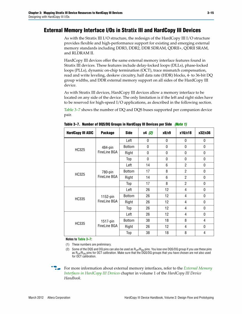
Chapter 3: Mapping Stratix III Device Resources to HardCopy III Devices 3–15Designing with HardCopy III I/Os
External Memory Interface I/Os in Stratix III and HardCopy III DevicesAs with the Stratix III I/O structure, the redesign of the HardCopy III I/O structure provides flexible and high-performance support for existing and emerging external memory standards including DDR3, DDR2, DDR SDRAM, QDRII+, QDRII SRAM, and RLDRAM II.
HardCopy III devices offer the same external memory interface features found in Stratix III devices. These features include delay-locked loops (DLLs), phase-locked loops (PLLs), dynamic on-chip termination (OCT), trace mismatch compensation, read and write leveling, deskew circuitry, half data rate (HDR) blocks, 4- to 36-bit DQ group widths, and DDR external memory support on all sides of the HardCopy III device.
As with Stratix III devices, HardCopy III devices allow a memory interface to be located on any side of the device. The only limitation is if the left and right sides have to be reserved for high-speed I/O applications, as described in the following section.
Table 3–7 shows the number of DQ and DQS buses supported per companion device pair.
f For more information about external memory interfaces, refer to the External Memory Interfaces in HardCopy III Devices chapter in volume 1 of the HardCopy III Device Handbook.
Table 3–7. Number of DQS/DQ Groups in HardCopy III Devices per Side (Note 1)
HardCopy III ASIC Package Side x4 (2) x8/x9 x16/x18 x32/x36
HC325 484-pin FineLine BGA
Left 0 0 0 0
Bottom 0 0 0 0
Right 0 0 0 0
Top 0 0 0 0
HC325 780-pin FineLine BGA
Left 14 6 2 0
Bottom 17 8 2 0
Right 14 6 2 0
Top 17 8 2 0
HC335 1152-pin FineLine BGA
Left 26 12 4 0
Bottom 26 12 4 0
Right 26 12 4 0
Top 26 12 4 0
HC335 1517-pin FineLine BGA
Left 26 12 4 0
Bottom 38 18 8 4
Right 26 12 4 0
Top 38 18 8 4
Notes to Table 3–7:
(1) These numbers are preliminary.(2) Some of the DQS and DQ pins can also be used as RUP/RDN pins. You lose one DQS/DQ group if you use these pins
as RUP/RDN pins for OCT calibration. Make sure that the DQS/DQ groups that you have chosen are not also used for OCT calibration.
March 2012 Altera Corporation HardCopy III Device Handbook, Volume 2: Design Flow and Prototyping

3–16 Chapter 3: Mapping Stratix III Device Resources to HardCopy III DevicesDesigning with HardCopy III I/Os
Mapping Stratix III High-Speed Differential I/O Interfaces with HardCopy III Devices
HardCopy III ASICs have the same dedicated circuitry as Stratix III devices for high-speed differential I/O support:
■ Differential I/O buffer
■ Transmitter serializer
■ Receiver deserializer
■ Data realignment
■ Dynamic phase aligner (DPA)
■ Synchronizer (FIFO buffer)
■ Analog PLLs (located on left and right sides of the device)
For high-speed differential interfaces, HardCopy III devices support the following differential I/O standards:
■ Low-voltage differential signaling (LVDS)
■ Mini-LVDS
■ Reduced swing differential signaling (RSDS)
■ Differential HSTL
■ Differential SSTL
HardCopy III ASICs support LVDS on all I/O banks. True LVDS makes use of dedicated LVDS I/O buffers that are optimized for performance. There are true LVDS input and output buffers at the left and right side I/O banks. There are true LVDS input buffers on the top and bottom I/O banks only.
You can configure all I/Os in all banks as emulated LVDS output buffers. Emulated output buffers make use of single-ended buffers and an external resistor network to mimic LVDS operation. Emulated LVDS is useful for low-speed, low-voltage differential applications.
f For more information about high-speed I/O performance, refer to the DC and Switching Characteristics of HardCopy III Devices chapter in volume 3 of the HardCopy III Device Handbook.
All dedicated circuitry for high-speed differential I/O applications are located in the left and right I/O banks of the Stratix III and HardCopy III devices. The top and bottom I/O banks also have support for high-speed receiver applications that do not require the use of the DPA, synchronizer, data realignment, and differential termination. Top and bottom differential I/O buffers have a slower data rate than the high-speed receivers on the left and right I/O banks.
HardCopy III Device Handbook, Volume 2: Design Flow and Prototyping March 2012 Altera Corporation

Chapter 3: Mapping Stratix III Device Resources to HardCopy III Devices 3–17Designing with HardCopy III I/Os
Table 3–8 and Table 3–9 show the LVDS channels supported in HardCopy III and Stratix III companion devices for socket replacement and non-socket replacement flows, respectively.
Table 3–8. LVDS Channels Supported In HardCopy III and Stratix III Companion Devices with Socket Replacement Flow (Part 1 of 2) (Note 1), (2)
Bank
780-Pin FineLine BGA 1152-Pin FineLine BGA 1517-Pin FineLine BGA
HardCopy IIIASIC
Stratix III FPGA
Prototype
HardCopy III ASIC
Stratix III FPGA
Prototype
HardCopy III ASIC
Stratix IIIFPGA
Prototype
HC325
EP3SL110EP3SL150EP3SE110
EP3SL200 (3)EP3SE260 (3)
HC335
EP3SL150EP3SE110EP3SL200EP3SE260
EP3SL340 (4)
HC335EP3SL200EP3SE260EP3SL340
1A 8Rx + 8Tx (5) 8Rx + 8Tx 12Rx + 12Tx 12Rx + 12Tx 12Rx + 12Tx 12Rx + 12Tx
1B — — — — — 6Rx + 6Tx
1C 6Rx + 6Tx 6Rx + 6Tx 10Rx + 10Tx 10Rx + 10Tx 10Rx + 10Tx 10Rx + 10Tx
2A 8Rx + 8Tx (5) 8Rx + 8Tx 12Rx + 12Tx 12Rx + 12Tx 12Rx + 12Tx 12Rx + 12Tx
2B — — — — — 6Rx + 6Tx
2C 6Rx + 6Tx 6Rx + 6Tx 10Rx + 10Tx 10Rx + 10Tx 10Rx + 10Tx 10Rx + 10Tx
3A (5)
10Rx + 10eTx
or
20eTx
10Rx + 10eTx
or
20eTx
10Rx + 10eTx
or
20eTx
10Rx + 10eTx
or
20eTx
12Rx + 12eTx
or
24eTx
12Rx + 12eTx
or
24eTx
3B (5) — —
6Rx + 6eTx
or
12eTx
6Rx + 6eTx
or
12eTx
12Rx + 12eTx
or
24eTx
12Rx + 12eTx
or
24eTx
3C (5)
6Rx + 6eTx
or
12eTx
6Rx + 6eTx
or
12eTx
8Rx + 8eTx
or
16eTx
8Rx + 8eTx
or
16eTx
8Rx + 8eTx
or
16eTx
8Rx + 8eTx
or
16eTx
4A (5)
10Rx + 10eTx
or
20eTx
10Rx + 10eTx
or
20eTx
10Rx + 10eTx
or
20eTx
10Rx + 10eTx
or
20eTx
12Rx + 12eTx
or
24eTx
12Rx + 12eTx
or
24eTx
4B (5) — —
6Rx + 6eTx
or
12eTx
6Rx + 6eTx
or
12eTx
12Rx + 12eTx
or
24eTx
12Rx + 12eTx
or
24eTx
4C (5)
6Rx + 6eTx
or
12eTx
6Rx + 6eTx
or
12eTx
8Rx + 8eTx
or
16eTx
8Rx + 8eTx
or
16eTx
8Rx + 8eTx
or
16eTx
8Rx + 8eTx
or
16eTx
5A 8Rx + 8Tx (6) 8Rx + 8Tx 12Rx + 12Tx 12Rx + 12Tx 12Rx + 12Tx 12Rx + 12Tx
5B — — — — — 6Rx + 6Tx
5C 6Rx + 6Tx 6Rx + 6Tx 10Rx + 10Tx 10Rx + 10Tx 10Rx + 10Tx 10Rx + 10Tx
6A 8Rx + 8Tx (6) 8Rx + 8Tx 12Rx + 12Tx 12Rx + 12Tx 12Rx + 12Tx 12Rx + 12Tx
6B — — — — — 6Rx + 6Tx
March 2012 Altera Corporation HardCopy III Device Handbook, Volume 2: Design Flow and Prototyping

3–18 Chapter 3: Mapping Stratix III Device Resources to HardCopy III DevicesDesigning with HardCopy III I/Os
6C 6Rx + 6Tx 6Rx + 6Tx 10Rx + 10Tx 10Rx + 10Tx 10Rx + 10Tx 10Rx + 10Tx
7A (5)
10Rx + 10eTx
or
20eTx
10Rx + 10eTx
or
20eTx
10Rx + 10eTx
or
20eTx
10Rx + 10eTx
or
20eTx
12Rx + 12eTx
or
24eTx
12Rx + 12eTx
or
24eTx
7B (5) — —
6Rx + 6eTx
or
12eTx
6Rx + 6eTx
or
12eTx
12Rx + 12eTx
or
24eTx
12Rx + 12eTx
or
24eTx
7C (5)
6Rx + 6eTx
or
12eTx
6Rx + 6eTx
or
12eTx
8Rx + 8eTx
or
16eTx
8Rx + 8eTx
or
16eTx
8Rx + 8eTx
or
16eTx
8Rx + 8eTx
or
16eTx
8A (5)
10Rx + 10eTx
or
20eTx
10Rx + 10eTx
or
20eTx
10Rx + 10eTx
or
20eTx
10Rx + 10eTx
or
20eTx
12Rx + 12eTx
or
24eTx
12Rx + 12eTx
or
24eTx
8B (5) — —
6Rx + 6eTx
or
12eTx
6Rx + 6eTx
or
12eTx
12Rx + 12eTx
or
24eTx
12Rx + 12eTx
or
24eTx
8C (5)
6Rx + 6eTx
or
12eTx
6Rx + 6eTx
or
12eTx
8Rx + 8eTx
or
16eTx
8Rx + 8eTx
or
16eTx
8Rx + 8eTx
or
16eTx
8Rx + 8eTx
or
16eTx
Notes to Table 3–8:
(1) Channel counts are preliminary.(2) Rx = true LVDS input buffers, Tx = true LVDS output buffers and eTx = emulated-LVDS output buffers, either LVDS_E3R or LVDS_E1R.(3) The EP3SE260 and EP3SL200 FPGAs are offered only in the H780 package.(4) The EP3SL340 FPGA is offered only in the H1152 package.(5) Top and bottom I/O banks do not have DPA, synchronizer, data realignment, and differential termination support in Stratix III and HardCopy III
devices. Use left and right I/O banks if these features and maximum performance is required.(6) When the HardCopy III devices mapped to use 780-pin FineLine BGA Wire Bond package, I/O banks 1A, 2A, 5A, and 6A can support 6 pairs of
LVDS channel (6RX + 6Tx) only.
Table 3–8. LVDS Channels Supported In HardCopy III and Stratix III Companion Devices with Socket Replacement Flow (Part 2 of 2) (Note 1), (2)
Bank
780-Pin FineLine BGA 1152-Pin FineLine BGA 1517-Pin FineLine BGA
HardCopy IIIASIC
Stratix III FPGA
Prototype
HardCopy III ASIC
Stratix III FPGA
Prototype
HardCopy III ASIC
Stratix IIIFPGA
Prototype
HC325
EP3SL110EP3SL150EP3SE110
EP3SL200 (3)EP3SE260 (3)
HC335
EP3SL150EP3SE110EP3SL200EP3SE260
EP3SL340 (4)
HC335EP3SL200EP3SE260EP3SL340
HardCopy III Device Handbook, Volume 2: Design Flow and Prototyping March 2012 Altera Corporation

Chapter 3: Mapping Stratix III Device Resources to HardCopy III Devices 3–19Designing with HardCopy III I/Os
Table 3–9. LVDS Channels Supported In HardCopy III and Stratix III Companion Devices with Non-Socket Replacement Flow (Part 1 of 2) (Note 1), (2)
Bank
484-Pin FineLine BGA
780-Pin FineLine BGA
484-Pin FineLine BGA
1152-Pin FineLine BGA
780-Pin FineLine BGA
1152-Pin FineLine BGA
HardCopy III ASICStratix III
FPGA Prototype
HardCopy III ASIC
Stratix III FPGA
Prototype
HardCopy III ASIC
Stratix III FPGA Prototype
HC325
EP3SL110EP3SL150EP3SE110
EP3SL200 (3)EP3SE260 (3)
HC325 EP3SL340 (4) HC325 EP3SL340 (4)
1A 6Rx + 6Tx 8Rx + 8Tx 6Rx + 6Tx 12Rx + 12Tx 8Rx + 8Tx 12Rx + 12Tx
1B — — — — — —
1C 6Rx + 6Tx 6Rx + 6Tx 6Rx + 6Tx 10Rx + 10Tx 6Rx + 6Tx 10Rx + 10Tx
2A 6Rx + 6Tx 8Rx + 8Tx 6Rx + 6Tx 12Rx + 12Tx 8Rx + 8Tx 12Rx + 12Tx
2B — — — — — —
2C 6Rx + 6Tx 6Rx + 6Tx 6Rx + 6Tx 10Rx + 10Tx 6Rx + 6Tx 10Rx + 10Tx
3A (5) —
10Rx + 10eTx
or
20eTx
—
10Rx + 10eTx
or
20eTx
6Rx + 6eTx
or
12eTx
10Rx + 10eTx
or
20eTx
3B (5) — — —
6Rx + 6eTx
or
12eTx
—
6Rx + 6eTx
or
12eTx
3C (5)
6Rx + 6eTx
or
12eTx
6Rx + 6eTx
or
12eTx
6Rx + 6eTx
or
12eTx
8Rx + 8eTx
or
16eTx
6Rx + 6eTx
or
12eTx
8Rx + 8eTx
or
16eTx
4A (5) —
10Rx + 10eTx
or
20eTx
—
10Rx + 10eTx
or
20eTx
6Rx + 6eTx
or
12eTx
10Rx + 10eTx
or
20eTx
4B (5) — — —
6Rx + 6eTx
or
12eTx
—
6Rx + 6eTx
or
12eTx
4C (5)
6Rx + 6eTx
or
12eTx
6Rx + 6eTx
or
12eTx
6Rx + 6eTx
or
12eTx
8Rx + 8eTx
or
16eTx
6Rx + 6eTx
or
12eTx
8Rx + 8eTx
or
16eTx
5A 6Rx + 6Tx 8Rx + 8Tx 6Rx + 6Tx 12Rx + 12Tx 8Rx + 8Tx 12Rx + 12Tx
5B — — — — — —
5C 6Rx + 6Tx 6Rx + 6Tx 6Rx + 6Tx 10Rx + 10Tx 6Rx + 6Tx 10Rx + 10Tx
6A 6Rx + 6Tx 8Rx + 8Tx 6Rx + 6Tx 12Rx + 12Tx 8Rx + 8Tx 12Rx + 12Tx
6B — — — — — —
6C 6Rx + 6Tx 6Rx + 6Tx 6Rx + 6Tx 10Rx + 10Tx 6Rx + 6Tx 10Rx + 10Tx
March 2012 Altera Corporation HardCopy III Device Handbook, Volume 2: Design Flow and Prototyping

3–20 Chapter 3: Mapping Stratix III Device Resources to HardCopy III DevicesHardCopy III PLL Planning and Utilization
HardCopy III PLL Planning and UtilizationHardCopy III devices offer up to 12 PLLs that support the same features as Stratix III PLLs. The same nomenclature is used for HardCopy III and Stratix III PLLs that follow their geographical location in the device floorplan. The PLLs that reside on the top and bottom sides of the device are named PLL_T1, PLL_T2, PLL_B1, and PLL_B2; the PLLs that reside on the left and right sides of the device are named PLL_L1, PLL_L2,
7A (5) —
10Rx + 10eTx
or
20eTx
—
10Rx + 10eTx
or
20eTx
6Rx + 6eTx
or
12eTx
10Rx + 10eTx
or
20eTx
7B (5) — — —
6Rx + 6eTx
or
12eTx
—
6Rx + 6eTx
or
12eTx
7C (5)
6Rx + 6eTx
or
12eTx
6Rx + 6eTx
or
12eTx
6Rx + 6eTx
or
12eTx
8Rx + 8eTx
or
16eTx
6Rx + 6eTx
or
12eTx
8Rx + 8eTx
or
16eTx
8A (5) —
10Rx + 10eTx
or
20eTx
—
10Rx + 10eTx
or
20eTx
6Rx + 6eTx
or
12eTx
10Rx + 10eTx
or
20eTx
8B (5) — — —
6Rx + 6eTx
or
12eTx
—
6Rx + 6eTx
or
12eTx
8C (5) 6Rx 6Rx 6Rx 8Rx 6Rx 8Rx
Notes to Table 3–9:
(1) Channel counts are preliminary.(2) Rx = true LVDS input buffers, Tx = true LVDS output buffers and eTx = emulated-LVDS output buffers, either LVDS_E3R or LVDS_E1R.(3) The EP3SE260 and EP3SL200 FPGAs are offered only in the H780 package.(4) The EP3SL340 FPGA is offered only in the H1152 package.(5) Top and bottom I/O banks do not have DPA, synchronizer, data realignment, and differential termination support in Stratix III and HardCopy III
devices. Use left and right I/O banks if these features and maximum performance is required.
Table 3–9. LVDS Channels Supported In HardCopy III and Stratix III Companion Devices with Non-Socket Replacement Flow (Part 2 of 2) (Note 1), (2)
Bank
484-Pin FineLine BGA
780-Pin FineLine BGA
484-Pin FineLine BGA
1152-Pin FineLine BGA
780-Pin FineLine BGA
1152-Pin FineLine BGA
HardCopy III ASICStratix III
FPGA Prototype
HardCopy III ASIC
Stratix III FPGA
Prototype
HardCopy III ASIC
Stratix III FPGA Prototype
HC325
EP3SL110EP3SL150EP3SE110
EP3SL200 (3)EP3SE260 (3)
HC325 EP3SL340 (4) HC325 EP3SL340 (4)
HardCopy III Device Handbook, Volume 2: Design Flow and Prototyping March 2012 Altera Corporation

Chapter 3: Mapping Stratix III Device Resources to HardCopy III Devices 3–21HardCopy III PLL Planning and Utilization
PLL_L3, PLL_L4, PLL_R1, PLL_R2, PLL_R3, and PLL_R4, respectively. Table 3–10 lists the number of PLLs available in HardCopy III devices and their companion Stratix III devices for the socket replacement flow.
Table 3–11 lists the number of PLLs available in HardCopy III devices and their companion Stratix III devices for the non-socket replacement flow.
Table 3–10. HardCopy III and Stratix III PLL Mapping Options for Socket Replacement Flow (Note 1)
PLL
780-Pin FineLine BGA 1152-Pin FineLine BGA 1517-Pin FineLine BGA
HardCopy III ASIC
Stratix III FPGA Prototype
HardCopy III ASIC
Stratix III FPGA Prototype
HardCopy III ASIC
Stratix III FPGA Prototype
HC325
EP3SL110EP3SL150EP3SE110
EP3SL200 (2)EP3SE260 (2)
HC335
EP3SL150EP3SE110EP3SL200EP3SE260
EP3SL340 (3)
HC335EP3SL200EP3SE260EP3SL340
PLL_L1 — — — — v vPLL_L2 v v v v v vPLL_L3 — — v v v vPLL_L4 — — — — v vPLL_T1 v v v v v vPLL_T2 — — v v v vPLL_B1 v v v v v vPLL_B2 — — v v v vPLL_R1 — — — — v vPLL_R2 v v v v v vPLL_R3 — — v v v vPLL_R4 — — — — v vNotes to Table 3–10:
(1) The PLL availability table is preliminary. It is best to design with the Quartus II software to check if your design can use all available PLLs.(2) The EP3SE260 and EP3SL200 FPGAs are offered only in the H780 package. (3) The EP3SL340 FPGA is offered only in the H1152 package.
Table 3–11. HardCopy III and Stratix III PLL Mapping Options for Non-Socket Replacement Flow (Part 1 of 2) (Note 1)
PLL
484-Pin FineLine BGA
780-Pin Fineline BGA
484-Pin FineLine BGA
1152-Pin Fineline BGA
780-Pin Fineline BGA
1152-Pin Fineline BGA
HardCopy III ASIC
Stratix III FPGA Prototype
HardCopy III ASIC
Stratix III FPGA Prototype
HardCopy III ASIC
Stratix III FPGA Prototype
HC325
EP3SL110EP3SL150EP3SE110
EP3SL200 (2)EP3SE260 (2)
HC325 EP3SL340 (3) HC325 EP3SL340 (3)
PLL_L1 — — — — — —
PLL_L2 v v v v v vPLL_L3 — — — v — v
March 2012 Altera Corporation HardCopy III Device Handbook, Volume 2: Design Flow and Prototyping

3–22 Chapter 3: Mapping Stratix III Device Resources to HardCopy III DevicesHardCopy III Memory Blocks
f For more information about HardCopy III PLLs, refer to the Clock Networks and PLLs in HardCopy III Devices chapter in volume 1 of the HardCopy III Device Handbook.
HardCopy III Memory Blocks TriMatrix memory in HardCopy III devices supports the same memory functions and features as Stratix III devices. You can independently configure each embedded memory block to be a single- or dual-port RAM, FIFO, ROM, or shift register using the MegaWizard™ Plug-In Manager in the Quartus II software.
HardCopy III embedded memory consists of MLAB, M9K, and M144K memory blocks, and has one-to-one mapping from Stratix III memory. However, the number of available memory blocks differs based on physical density, package, and Stratix III device to HardCopy III ASIC mapping paths. The Quartus II software may not allow all available Stratix III memory types to fit into a selected HardCopy III device if your design has a very high resource utilization and performance target.
1 Altera recommends that you compile your design with the Quartus II software and verify the device resource guide to check for available resources in the HardCopy III device.
f For information about using the HardCopy Device Resource Guide, refer to the Quartus II Support for HardCopy Series Devices chapter in volume 1 of the Quartus II Handbook.
PLL_L4 — — — — — —
PLL_T1 v v v v v vPLL_T2 — — — v — vPLL_B1 v v v v v vPLL_B2 — — — v — vPLL_R1 — — — — — —
PLL_R2 v v v v v vPLL_R3 — — — v — vPLL_R4 — — — — — —
Notes to Table 3–11:
(1) The PLL availability table is preliminary. It is best to design with the Quartus II software to check if your design can use all available PLLs.(2) The EP3SL200 and EP3SE260 FPGAs are offered only in the H780 package.(3) The EP3SL340 FPGA is offered only in the H1152 package.
Table 3–11. HardCopy III and Stratix III PLL Mapping Options for Non-Socket Replacement Flow (Part 2 of 2) (Note 1)
PLL
484-Pin FineLine BGA
780-Pin Fineline BGA
484-Pin FineLine BGA
1152-Pin Fineline BGA
780-Pin Fineline BGA
1152-Pin Fineline BGA
HardCopy III ASIC
Stratix III FPGA Prototype
HardCopy III ASIC
Stratix III FPGA Prototype
HardCopy III ASIC
Stratix III FPGA Prototype
HC325
EP3SL110EP3SL150EP3SE110
EP3SL200 (2)EP3SE260 (2)
HC325 EP3SL340 (3) HC325 EP3SL340 (3)
HardCopy III Device Handbook, Volume 2: Design Flow and Prototyping March 2012 Altera Corporation

Chapter 3: Mapping Stratix III Device Resources to HardCopy III Devices 3–23HardCopy III Memory Blocks
Functionally, memory in HardCopy III and Stratix III devices is identical. Memory blocks can implement various types of memory with or without parity, including true dual-port, simple dual-port, and single-port RAM, ROM, and FIFO.
c When using the memory blocks in ROM, single-port, simple dual-port, or true dual-port mode, you can corrupt the memory contents if you violate the setup or hold-time on any of the memory block input registers. This applies to both read and write operations.
MLAB ImplementationIn Stratix III devices, MLABs are dedicated blocks and can be configured for regular logic functions or memory functions. In HardCopy III devices, MLAB memory blocks are implemented using HCells. The Quartus II software maps the Stratix III MLAB function to the appropriate memory HCell macro that preserves memory function. This allows you to use the HardCopy III core fabric more efficiently, freeing up unused HCells for ALM or DSP functions.
MLAB, M9K, and M144K Utilization HardCopy III MLAB, M9K, and M144K block functionality is similar to Stratix III memory blocks; however, you cannot pre-load HardCopy III MLAB, M9K, and M144K blocks with a .mif file when using them as RAM. Ensure that your Stratix III design does not require .mif files if the memory blocks are used as RAM. However, if memory blocks are used as ROM, they are mask-programmed to the design’s ROM contents.
1 You can use the ALTMEM_INIT megafunction to initialize a RAM block after power-up for Stratix III and HardCopy III devices. This megafunction reads from a ROM defined with the megafunction and writes to the RAM after power-up. This function allows you to have initialized contents on a RAM block. Refer to the Quartus II Help for implementation information about this function.
Unlike Stratix III FPGAs, HardCopy III MLAB, M9K, and M144K RAM contents are unknown after power-up. However, like Stratix III devices, all HardCopy III memory output registers power-up cleared, if used. When designing HardCopy III memory blocks as RAM, Altera recommends a write-before-read of the memory block to avoid reading unknown initial power-up data conditions. If the HardCopy III memory block is designated as ROM, it powers up with the ROM contents.
One advantage over Stratix III RAM blocks is that unused M9K and M144K blocks are disconnected from the power rails and MLABs are only implemented as required by your design. These unused resources do not contribute to overall power consumption on HardCopy III devices.
f For a list of supported features in HardCopy III memory blocks, refer to the TriMatrix Embedded Memory Blocks in HardCopy III Devices chapter in volume 1 of the HardCopy III Device Handbook.
March 2012 Altera Corporation HardCopy III Device Handbook, Volume 2: Design Flow and Prototyping
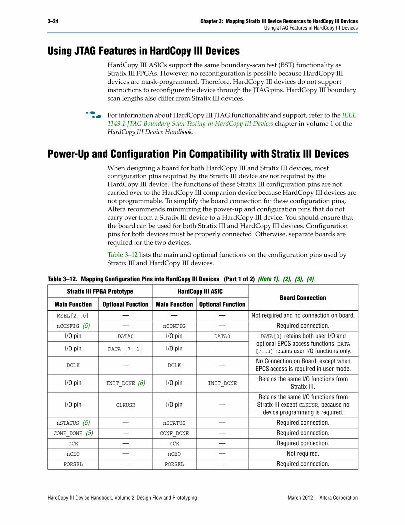
3–24 Chapter 3: Mapping Stratix III Device Resources to HardCopy III DevicesUsing JTAG Features in HardCopy III Devices
Using JTAG Features in HardCopy III DevicesHardCopy III ASICs support the same boundary-scan test (BST) functionality as Stratix III FPGAs. However, no reconfiguration is possible because HardCopy III devices are mask-programmed. Therefore, HardCopy III devices do not support instructions to reconfigure the device through the JTAG pins. HardCopy III boundary scan lengths also differ from Stratix III devices.
f For information about HardCopy III JTAG functionality and support, refer to the IEEE 1149.1 JTAG Boundary Scan Testing in HardCopy III Devices chapter in volume 1 of the HardCopy III Device Handbook.
Power-Up and Configuration Pin Compatibility with Stratix III DevicesWhen designing a board for both HardCopy III and Stratix III devices, most configuration pins required by the Stratix III device are not required by the HardCopy III device. The functions of these Stratix III configuration pins are not carried over to the HardCopy III companion device because HardCopy III devices are not programmable. To simplify the board connection for these configuration pins, Altera recommends minimizing the power-up and configuration pins that do not carry over from a Stratix III device to a HardCopy III device. You should ensure that the board can be used for both Stratix III and HardCopy III devices. Configuration pins for both devices must be properly connected. Otherwise, separate boards are required for the two devices.
Table 3–12 lists the main and optional functions on the configuration pins used by Stratix III and HardCopy III devices.
Table 3–12. Mapping Configuration Pins into HardCopy III Devices (Part 1 of 2) (Note 1), (2), (3), (4)
Stratix III FPGA Prototype HardCopy III ASICBoard Connection
Main Function Optional Function Main Function Optional Function
MSEL[2..0] — — — Not required and no connection on board.
nCONFIG (5) — nCONFIG — Required connection.
I/O pin DATA0 I/O pin DATA0 DATA[0] retains both user I/O and optional EPCS access functions. DATA [7..1] retains user I/O functions only.I/O pin DATA [7..1] I/O pin —
DCLK — DCLK — No Connection on Board, except when EPCS access is required in user mode.
I/O pin INIT_DONE (6) I/O pin INIT_DONERetains the same I/O functions from
Stratix III.
I/O pin CLKUSR I/O pin —Retains the same I/O functions from Stratix III except CLKUSR, because no
device programming is required.
nSTATUS (5) — nSTATUS — Required connection.
CONF_DONE (5) — CONF_DONE — Required connection.
nCE — nCE — Required connection.
nCEO — nCEO — Not required.
PORSEL — PORSEL — Required connection.
HardCopy III Device Handbook, Volume 2: Design Flow and Prototyping March 2012 Altera Corporation

Chapter 3: Mapping Stratix III Device Resources to HardCopy III Devices 3–25Power-Up and Configuration Pin Compatibility with Stratix III Devices
I/O pin ASDO I/O pin ASDONo connection on board, except when EPCS access is required in user mode.
I/O pin nCSO I/O pin nCSONo connection on board, except when EPCS access is required in user mode.
nIO_PULLUP — nIO_PULLUP — Required connection.
I/O pin CRC_ERROR (4) I/O pin —Retains the same I/O functions from
Stratix III, but not CRC_ERROR, because no device programming is required.
I/O pin DEV_CLRn I/O pin DEV_CLRnRetains the same I/O functions from
Stratix III.
I/O pin DEV_OE I/O pin DEV_OERetains the same I/O functions from
Stratix III.
Notes to Table 3–12:
(1) For correct operation of a HardCopy III device, pull the nSTATUS, nCONFIG, and CONF_DONE pins to VCCPGM. In HardCopy III devices, these pins are designed with weak internal resistors pulled up to VCCPGM. Stratix III configuration schemes require pull-up resistors on these I/O pins, so they may already be present on the board. You can remove these external pull-up resistors, if doing so does not affect other FPGAs on the board.
(2) HardCopy III devices have a maximum VCCIO voltage of 3.0 V, but the input I/O pin can tolerate a 3.3 V level. This applies to VCCPGM voltage and all dedicated and dual-purpose pins.
(3) For HardCopy III devices, there is weak pull-up on the nSTATUS, CONF_DONE, nCONFIG, and DCLK pins. Therefore, these pins can be left floating or remain connected to external pull-up resistors. If the EPCS is used in user mode as a boot-up RAM or data access for a Nios® II processor, DCLK, DATA[0], ASDO, and nCSO must be connected to the EPCS device.
(4) In HardCopy III devices, CRC_ERROR is hard-wired to logic 0 if the CRC feature is enabled in Stratix III devices.(5) The PORSEL pin setting delays the POR sequence for both HardCopy III and Stratix III devices.(6) The INIT_DONE settings option is mask-programmed into the device. You must submit these settings to Altera with the final design prior to
mapping to a HardCopy III device. The use of the INIT_DONE option and other dual-purpose pins (for example, DEV_CLRn device-wide reset and DEV_OE device-wide output enable) are available in the Fitter Device Options section of the Quartus II report file.
Table 3–12. Mapping Configuration Pins into HardCopy III Devices (Part 2 of 2) (Note 1), (2), (3), (4)
Stratix III FPGA Prototype HardCopy III ASICBoard Connection
Main Function Optional Function Main Function Optional Function
March 2012 Altera Corporation HardCopy III Device Handbook, Volume 2: Design Flow and Prototyping

3–26 Chapter 3: Mapping Stratix III Device Resources to HardCopy III DevicesPower-Up and Configuration Pin Compatibility with Stratix III Devices
For both the Stratix III and HardCopy III devices, the Quartus II software allows you to set the I/O pins listed in Table 3–12 as dual-purpose pins (as shown in Figure 3–2). As dual-purpose pins, they have I/O functionality when the device enters user mode (when INIT_DONE is asserted).
If these dual-purpose pins are required to configure the Stratix III device, but will be unused after configuration, these pins remain unused on the HardCopy III device. It is important to consider the state of these pins after power-up and when the device is in user mode. For example, when replacing the Stratix III device with a HardCopy III device, these pins may be left floating when the configuration device is removed if you assign such pins as inputs. In this case, you will either require an external means to drive them to a stable level, or set the pins to output driving ground.
Figure 3–2. Device and Pin Options Dialog Box
HardCopy III Device Handbook, Volume 2: Design Flow and Prototyping March 2012 Altera Corporation
Chapter 3: Mapping Stratix III Device Resources to HardCopy III Devices 3–27Revision History
Revision HistoryTable 3–13 shows the revision history for this document.
Table 3–13. Document Revision History
Date Version Changes
March 2012 3.3 Updated Table 3–1, Table 3–2, Table 3–3, Table 3–5, Table 3–7, Table 3–9, and Table 3–11: removed device HC315.
January 2011 3.2 Minor text edits.
January 2010 3.1 ■ Updated Table 3–20, Table 3–21, and Table 3–29.
June 2009 3.0
■ Updated the following tables: Table 3–1, Table 3–4, Table 3–7, Table 3–10, Table 3–6, Table 3–16, Table 3–18, Table 3–10, and Table 3–12
■ Added the following tables: Table 3–11, Table 3–19, Table 3–11
■ Updated Figure 3–1
■ Updated “HardCopy III and Stratix III Mapping Options” on page 3–3
■ Updated “Mapping HardCopy III and Stratix III I/Os and Modular I/O Banks” on page 3–9
■ Removed “Referenced Documents”
■ This chapter was listed as p/n 52003 in document release version 2.0
December 2008 2.0 Minor text edits.
May 2008 1.0 Initial release.
March 2012 Altera Corporation HardCopy III Device Handbook, Volume 2: Design Flow and Prototyping

3–28 Chapter 3: Mapping Stratix III Device Resources to HardCopy III DevicesRevision History
HardCopy III Device Handbook, Volume 2: Design Flow and Prototyping March 2012 Altera Corporation

HardCopy III Device Handbook, Volume 2: Design FloMarch 2012
HIII53004-3.2
© 2012 Altera Corporation. All rights reserved. ALTERA, ARRand/or trademarks of Altera Corporation in the U.S. and otherwww.altera.com/common/legal.html. Altera warrants performreserves the right to make changes to any products and servicesinformation, product, or service described herein except as expspecifications before relying on any published information and
March 2012HIII53004-3.2
4. Matching Stratix III Power andConfiguration Requirements with
HardCopy III Devices
This chapter discusses power-up options for HardCopy® III devices and provides examples of how to replace FPGAs in the system with HardCopy III devices.
Configuring an FPGA is the process of loading the design data into the device. The Altera® SRAM-based Stratix® III FPGA requires configuration each time the device is powered up. After the device is powered down, the configuration data within the Stratix III device is lost and must be loaded again on power up.
HardCopy III devices are mask-programmed and do not require configuration. One of the advantages of HardCopy III devices is their instant-on capability upon power up. In addition, there are options to increase delay to postpone HardCopy III devices power up.
HardCopy III Power-Up OptionsHardCopy III devices feature two power-up modes:
■ Instant On (no added delay)
■ Instant On After 50 ms Delay
The intent of the power-up modes is to give customers the option of choosing between Instant On and Instant On After 50 ms Delay.
Instant On mode is the fastest power-up option on a HardCopy III device. This mode is used when the HardCopy III device powers up independently while other components on the board require initialization and configuration. Therefore, you must verify that all signals which propagate to and from the HardCopy III device (for example, reference clocks and other input pins) are stable and do not interrupt HardCopy III device operation.
Some customers use Instant On After 50 ms Delay mode because the system might require the FPGA and HardCopy III devices to wait until a neighboring processor initializes completely. This mode holds the design in reset for 50 ms prior to startup. In addition to the considerations of the system, the software expects the delay from the FPGA device, which will now be replaced with the HardCopy device, and in these cases, customers choose this option.
1 You must choose the power-up option when submitting the design database to Altera for HardCopy III devices. After the HardCopy III devices are manufactured, the power-up option cannot be changed.
Instant On mode is the traditional power-up scheme of most ASIC and non-volatile devices. Similar to Stratix III devices, HardCopy III devices go through four phases before transitioning to user mode. However, because HardCopy III devices do not require configuration, the configuration phase is replaced by a delay phase with either no added delay or a 50 ms delay.
w and Prototyping
Subscribe
IA, CYCLONE, HARDCOPY, MAX, MEGACORE, NIOS, QUARTUS and STRATIX are Reg. U.S. Pat. & Tm. Off. countries. All other trademarks and service marks are the property of their respective holders as described at
ance of its semiconductor products to current specifications in accordance with Altera’s standard warranty, but at any time without notice. Altera assumes no responsibility or liability arising out of the application or use of any ressly agreed to in writing by Altera. Altera customers are advised to obtain the latest version of device before placing orders for products or services.

4–2 Chapter 4: Matching Stratix III Power and Configuration Requirements with HardCopy III DevicesHardCopy III Power-Up Options
The four phases are listed in order:
■ Power-up phase
■ Initialization phase
■ Delay phase (replacing the configuration phase)
■ Start-up phase
Instant On (No Added Delay)In Instant On mode, after the power supplies ramp up above the HardCopy III device’s power-on reset (POR) trip point, the device initiates an internal POR sequence. After tPOR (as shown in Figure 4–1 and Figure 4–2), the power-up phase is complete and the HardCopy III device transitions to an initialization phase, which releases the CONF_DONE signal to be pulled high. Pulling the CONF_DONE signal high indicates that the HardCopy III device is nearly ready for normal operation. For more information, refer to Figure 4–1.
During the power-up sequence, weak internal pull-up resistors can pull the user I/O pins high. When the power-up and initialization phases are complete, the I/O pins are released. If the nIO_pullup pin transitions high, the weak pull-up resistors are disabled.
f You can find the value of the internal weak pull-up resistors on the I/O pins in the Operating Conditions table of the specific FPGA’s device handbook.
Instant On After 50 ms DelayThe Instant On After 50 ms delay mode is similar to Instant On mode. However, the device waits an additional 50 ms during delay phase before releasing the CONF_DONE pin. This delay is created by an on-chip oscillator. This option is beneficial if other devices on the board (such as a microprocessor) must be initialized prior to the normal operation of the HardCopy III device.
A start-up phase occurs immediately after the internal registers are reset, all PLLs used are initialized, and any I/O pins used are enabled as the device transitions into user mode.
HardCopy III Device Handbook, Volume 2: Design Flow and Prototyping March 2012 Altera Corporation

Chapter 4: Matching Stratix III Power and Configuration Requirements with HardCopy III Devices 4–3HardCopy III Power-Up Options
Figure 4–1 shows an Instant On power-up waveform in which the HardCopy III device is powered up and the nCONFIG, nSTATUS, and CONF_DONE pins are driven high externally. The values for these parameters are listed in Table 4–1.
Figure 4–2 shows an alternative to the power-up waveform shown in Figure 4–1. The nCONFIG pin is externally held low longer than the PORSEL delay. This delays the initialization sequence by a small amount.
Figure 4–1. Timing Waveform for Instant On Option (Note 1), (2), (3), (4), (5)
Notes to Figure 4–1:
(1) VCC (ALL) represents either all the power pins or the last power pin powered up to specified operating conditions.(2) The nCONFIG, nSTATUS, and CONF_DONE pins are weakly pulled high by an external 10 K ohm resistor to VCCPGM; they must be high for this
waveform to apply.(3) User I/O pins may be tri-stated or driven before and during power-up. The nIO_pullup pin can affect the state of the user I/O pins during the
initialization phase.(4) INIT_DONE is an optional pin that can be enabled on the FPGA using the Quartus® II software. HardCopy III devices carry over the INIT_DONE
functionality from the prototyped FPGA design.(5) The nCEO pin is asserted at approximately the same time as the CONF_DONE pin is released. However, the nCE pin must be driven low externally
for this waveform to apply.
Vcc (ALL)
nCONFIG
nSTATUS
CONF_DONE
User I/O
INIT_DONE
User ModeHigh-Z"don't care"
"don't care"
"don't care"
"don't care"
"don't care"
tUMtCDtADDtPOR
March 2012 Altera Corporation HardCopy III Device Handbook, Volume 2: Design Flow and Prototyping

4–4 Chapter 4: Matching Stratix III Power and Configuration Requirements with HardCopy III DevicesHardCopy III Power-Up Options
In addition, Figure 4–2 shows an Instant On power-up waveform where nCONFIG is momentarily held low and nSTATUS and CONF_DONE are driven high externally. The values for these parameters are listed in Table 4–1.
Figure 4–2. Timing Waveform for Instant On Option Where nCONFIG is Held Low After Power-Up
Notes to Figure 4–2:
(1) This waveform applies if nCONFIG is held low longer than tPOR delay.(2) VCC (ALL) represents either all the power pins or the last power pin powered up to specified operating conditions. All HardCopy III power pins
must be powered within specifications.(3) The nCONFIG, nSTATUS, and CONF_DONE pins are weakly pulled high by an external 10 K ohm resistor to VCCPGM; they must be high for this
waveform to apply.(4) User I/O pins may be tri-stated or driven before and during power-up.(5) INIT_DONE is an optional pin that can be enabled on the FPGA using the Quartus II software. HardCopy III devices carry over the INIT_DONE
functionality from the prototype FPGA design.(6) The nCEO pin is asserted at approximately the same time as the CONF_DONE pin is released. However, the nCE pin must be driven low externally
for this waveform to apply. Pulsing the nCONFIG signal on an FPGA re-initializes the configuration sequence. The nCONFIG signal on a HardCopy III device also restarts the initialization sequence.
Vcc (ALL)
nCONFIG
nSTATUS
CONF_DONE
User I/O
INIT_DONE
User ModeHigh-Z"don't care"
"don't care"
"don't care"
"don't care"
tUMtCDtADDtCF2ST1tPOR or Longer
HardCopy III Device Handbook, Volume 2: Design Flow and Prototyping March 2012 Altera Corporation

Chapter 4: Matching Stratix III Power and Configuration Requirements with HardCopy III Devices 4–5HardCopy III Power-Up Options
Pulsing the nCONFIG signal on an FPGA re-initializes the configuration sequence. This is the same for HardCopy ASIC devices; users pulse the nCONFIG signal on a HardCopy ASIC device and this also restarts the POR sequence. Figure 4–3 shows the Instant On behavior of the configuration signals and user I/O pins if the nCONFIG pin is pulsed while the VCC supplies are already powered up and stable. The values for these parameters are listed in Table 4–1.
f For more information about HardCopy III configuration specifications, refer to the DC and Switching Characteristics chapter in volume 3 of the HardCopy III Device Handbook and the Hot Socketing and Power-On Reset chapter in volume 1 of the HardCopy III Device Handbook.
Table 4–1 lists the timing parameters and their conditions during the power-up sequence for Figure 4–1 through Figure 4–3.
Figure 4–3. Timing Waveform for the Instant-On Option When Pulsing the nCONFIG Signal (Note 1), (2), (3), (4), (5)
Notes to Figure 4–3:
(1) VCC (ALL) represents either all the power pins or the last power pin powered up to specified operating conditions. All HardCopy III power pins must be powered within specifications as described in Hot Socketing sections.
(2) The nSTATUS and CONF_DONE pins must not be driven low externally for this waveform to apply.(3) The nIO_pullup pin can affect the state of the user I/O pins during the initialization phase.(4) INIT_DONE is an optional pin that can be enabled on the FPGA using the Quartus II software. HardCopy III devices carry over the INIT_DONE
functionality from the prototyped FPGA design.(5) The nCEO pin is asserted at approximately the same time as the CONF_DONE pin is released. However, the nCE pin must be driven low externally
for this waveform to apply.
Vcc (ALL)
nCONFIG
nSTATUS
CONF_DONE
User I/O
INIT_DONE
User ModeHigh Z"don't care"
"don't care"
tUMtCDtADDtCF2ST1tCF2ST0
Table 4–1. Power-up Timing Parameters for HardCopy III Devices
Symbol Parameter Min Typ Max Units
tPOR PORSEL delayPORSEL = H 12 — — ms
PORSEL = L 100 — — ms
tCF2ST0 nCONFIG low to nSTATUS low — — 0.8 µs
tCF2ST1 nCONFIG high to nSTATUS high — — 270 µs
tADD Additional delayInstant on 50 — 90 µs
After 50 ms delay 50 — 90 ms
tCD CONF_DONE delay 0.6 — 1.1 µs
tUM User mode delay 50 — 110 µs
March 2012 Altera Corporation HardCopy III Device Handbook, Volume 2: Design Flow and Prototyping

4–6 Chapter 4: Matching Stratix III Power and Configuration Requirements with HardCopy III DevicesHardCopy III Power-Up Options
1 HardCopy III devices power up to user mode instantly, while a Stratix III device requires configuration after power up. If you are designing a board in which a HardCopy III device will replace the Stratix III device, ensure that all signals important to the HardCopy III device are ready before the HardCopy III device enters user mode. Examples of these signals are clocks, resets, and control signals. If these signals are not ready, system operation may be erratic until a proper reset and initialization of your design is performed.
Configuration Pin CompatibilityWhen designing a board for both a Stratix III prototype device and its companion HardCopy III device, most configuration pins required by the Stratix III device are not required by the HardCopy III device. The programmable capabilities of these configuration pins in Stratix III devices cannot carry over to the HardCopy III companion device because the HardCopy III device is not programmable. To simplify the board connection for these configuration pins, Altera recommends minimizing the power-up and configuration pins that do not carry over from the Stratix III device to the HardCopy III device.
Table 4–2 lists the dedicated and optional configuration pins for Stratix III and HardCopy III devices. If the HardCopy III device uses the pins’ optional function found in Stratix III devices, the Quartus II software allows you to set these pins as dual-purpose pins. As dual-purpose pins, they have I/O functionality after power up and initialization. These pins only switch to their I/O designation when the device enters user mode (when INIT_DONE is asserted). The design may require that some signals be present when the device transitions into user mode; therefore, it is important to consider the state of these pins after power up and after the device is in user mode when designing the board and selecting the state of dual-purpose pins.
Table 4–2. Configuration Pin Compatibility (Part 1 of 2) (Note 1), (2), (3)
Stratix III HardCopy III
Pin Name Function Board Connection
MSEL [2..0] Dedicated No connect on board
nCONFIG (5) Dedicated Required connection
DATA [7..0] Dual-Purpose DATA[0] retains both user I/O and optional EPCS access functions. DATA[7..1] retains user I/O functions only
DCLK Dedicated No connect on board, except when EPCS access is required in user mode
INIT_DONE (6) Dual-Purpose (Optional) Retains the same I/O functions from the Stratix III device
CLKUSR Dual-Purpose (Optional) Retains the same I/O functions from the Stratix III device
nSTATUS (5) Dedicated Required connection
CONF_DONE (5) Dedicated Required connection
nCE Dedicated Required connection
nCEO Dedicated Not required
PORSEL (5) Dedicated Required connection
ASDO Dedicated No connect on board, except when EPCS access is required in user mode
HardCopy III Device Handbook, Volume 2: Design Flow and Prototyping March 2012 Altera Corporation

Chapter 4: Matching Stratix III Power and Configuration Requirements with HardCopy III Devices 4–7HardCopy III Power-Up Options
f For more information about PORSEL settings for the FPGA, refer to the Configuration Handbook.
Most optional configuration pins listed in Table 4–2 on page 4–6 support the various configuration schemes available in Stratix III FPGAs. Parallel programming and remote update configuration modes use most of the pins in Table 4–2 on page 4–6. HardCopy III devices are not configurable and do not support configuration emulation mode. Therefore, Altera recommends that you minimize using the optional functionality of the configuration pin in the Stratix III design by using another mode such as passive serial configuration mode.
If some of these dual-purpose pins are needed to configure the Stratix III FPGA, but will be unused after configuration, these pins remain unused on the HardCopy III device. Therefore, use caution when designing for these pins on the Stratix III and HardCopy III boards. The removal of the Stratix III device and its corresponding configuration device may leave these pins floating on the HardCopy III device if you assign them as inputs without any external means of driving them to a stable level. When selecting a Stratix III device and its device options, consider the after-configuration requirements of these pins and set them appropriately in the Quartus II software.
nCSO Dedicated No connect on board, except when EPCS access is required in user mode
nIO_PULLUP Dedicated Required connection
CRC_ERROR (4) Dual-Purpose (Optional) Retains the same I/O functions from the Stratix III device, but not CRC_ERROR because no device programming is needed.
DEV_CLRn Dual-Purpose (Optional) Retains the same I/O functions from Stratix III
DEV_OE Dual-Purpose (Optional) Retains the same I/O functions from Stratix III
Notes to Table 4–2:
(1) For correct operation of the HardCopy III device, pull the nSTATUS, nCONFIG, and CONF_DONE pins to VCCPGM. In HardCopy III devices, these pins are designed with weak internal resistors pulled up to VCCPGM. Stratix III configuration schemes require pull-up resistors on these I/O pins, so they may already be present on the board. You can remove these external pull-up resistors if doing so does not affect other FPGAs on the board.
(2) HardCopy III devices have a maximum VCCIO voltage of 3.0 V, but the input I/O pin can tolerate a 3.3-V level. This applies to VCCPGM voltage and all dedicated and dual-purpose pins.
(3) For HardCopy III devices, there is weak pull-up on the nSTATUS, CONF_DONE, nCONFIG, and DCLK pins. Therefore, these pins can be left floating or remain connected to external pull-up resistors. If you use Erasable Programmable Configurable Serial (EPCS) in user mode as a boot-up RAM or data access for a Nios® II processor, DCLK, DATA[0], ASDO, and nCSO need to be connected to the EPCS device.
(4) In HardCopy III devices, CRC_ERROR is hard-wired to logic 0 if the CRC feature is enabled in Stratix III devices.(5) The PORSEL pin setting delays the POR sequence similar to the prototyping FPGA. (6) The INIT_DONE settings option is mask-programmed into the device. You must submit these settings to Altera with the final design prior to
mapping to a HardCopy III device. Using the INIT_DONE option and other dual-purpose pins (for example, the DEV_CLRn device-wide reset and DEV_OE device-wide output enable) are available in the Fitter Device Options section of the Quartus II report file.
Table 4–2. Configuration Pin Compatibility (Part 2 of 2) (Note 1), (2), (3)
Stratix III HardCopy III
Pin Name Function Board Connection
March 2012 Altera Corporation HardCopy III Device Handbook, Volume 2: Design Flow and Prototyping

4–8 Chapter 4: Matching Stratix III Power and Configuration Requirements with HardCopy III DevicesExamples of Mapping a Stratix FPGA Configuration to a HardCopy ASIC
Examples of Mapping a Stratix FPGA Configuration to a HardCopy ASICThis section provides examples of how HardCopy III devices replace Stratix III FPGAs using different configuration schemes.
HardCopy III Device Replacing a Stand-Alone Stratix III DeviceFigure 4–4 shows the Stratix III device before it is replaced with the HardCopy III device. The example in Figure 4–5 shows the single HardCopy III device replacing a stand-alone Stratix III device. The configuration device, now redundant, is removed, and no further board changes are necessary. You can remove he pull-up resistors on the nCONFIG, nSTATUS, and CONF_DONE pins.
Figure 4–4. Configuration of a Stand-Alone Stratix III Device
Figure 4–5. HardCopy III Device Replacing Stand-Alone Stratix III Device
Stratix III DeviceConfiguration
DeviceDCLKDATAOEnCSnINIT_CONF
MSEL
DCLKDATA0
nSTATUSCONF_DONE
nCONFIG
VCCPGM VCCPGM
GND
nCE
VCCPGM
nCEO
nCASC N.C.
N.C.
n
10 kΩ 10 kΩ 10 kΩ
HardCopy III Device
MSEL
DCLKDATA0
nSTATUSCONF_DONE
nCONFIG
VCCPGMVCCPGM
GND
nCE
VCCPGM
nCEO N.C.
N.C.N.C.
n
10 kΩ 10 kΩ 10 kΩ
HardCopy III Device Handbook, Volume 2: Design Flow and Prototyping March 2012 Altera Corporation
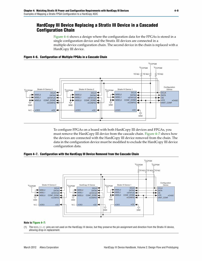
Chapter 4: Matching Stratix III Power and Configuration Requirements with HardCopy III Devices 4–9Examples of Mapping a Stratix FPGA Configuration to a HardCopy ASIC
HardCopy III Device Replacing a Stratix III Device in a Cascaded Configuration Chain
Figure 4–6 shows a design where the configuration data for the FPGAs is stored in a single configuration device and the Stratix III devices are connected in a multiple-device configuration chain. The second device in the chain is replaced with a HardCopy III device.
To configure FPGAs on a board with both HardCopy III devices and FPGAs, you must remove the HardCopy III device from the cascade chain. Figure 4–7 shows how the devices are connected with the HardCopy III device removed from the chain. The data in the configuration device must be modified to exclude the HardCopy III device configuration data.
Figure 4–6. Configuration of Multiple FPGAs in a Cascade Chain
ConfigurationDevice
DCLKDATAOEnCSnINIT_CONF
DCLKDATA0
nSTATUSCONF_DONE
nCONFIG
VCCPGM VCCPGM
GND
nCE
VCCPGM
DCLKDATA0
nSTATUSCONF_DONE
nCONFIGGND
nCE
MSEL2MSEL1
nCEO
nCASC
nCEO
MSEL0
VCCPGM
GND
MSEL2MSEL1
MSEL0
VCCPGM
10 kΩ10 kΩ 10 kΩ
DCLKDATA0
nSTATUSCONF_DONE
nCONFIGGND
nCE
MSEL2MSEL1
nCEO N.C.
Stratix III Device 3 Stratix III Device 2 Stratix III Device 1
MSEL0
VCCPGM
Figure 4–7. Configuration with the HardCopy III Device Removed from the Cascade Chain
Note to Figure 4–7:
(1) The MSEL[2:0] pins are not used on the HardCopy III device, but they preserve the pin assignment and direction from the Stratix III device, allowing drop-in replacement.
ConfigurationDevice
DCLKDATAOEnCSnINIT_CONF
DCLKDATA0
nSTATUSCONF_DONE
nCONFIG
VCCPGM VCCPGM
GNDGND
nCE
VCCPGM
DCLKDATA0
nSTATUSCONF_DONE
nCONFIGGND
nCE
MSEL2MSEL1
nCEO
nCASC
nCEO
MSEL0
VCCPGM
GND
MSEL2MSEL1
MSEL0
VCCPGM
10 kΩ 10 kΩ10 kΩ
DCLKDATA0
nSTATUSCONF_DONE
nCONFIGGND
nCE
MSEL2MSEL1
nCEO N.C. N.C.
Stratix III Device 2 HardCopy III Device Stratix III Device 1
MSEL0
VCCPGM
March 2012 Altera Corporation HardCopy III Device Handbook, Volume 2: Design Flow and Prototyping

4–10 Chapter 4: Matching Stratix III Power and Configuration Requirements with HardCopy III DevicesExamples of Mapping a Stratix FPGA Configuration to a HardCopy ASIC
Eliminating the HardCopy III device from the configuration chain requires the following changes:
■ The configuration data stored in the configuration device must be updated to exclude the configuration data for the HardCopy III device.
■ The nCE pin of the HardCopy III device must be tied to GND.
■ The nCE pin of the FPGA that was driven by the HardCopy III nCEO pin must now be driven by the nCEO pin of the FPGA that precedes the HardCopy III device in the chain.
■ The connections of the MSEL[2:0] pins are not required.
HardCopy III Device Replacing a Stratix III Device Configured with a Microprocessor
When you replace a Stratix III FPGA with a HardCopy III device, the microprocessor code must be modified to treat the HardCopy III device as a non-configurable device. Figure 4–8 shows an example with two Stratix III devices configured using a microprocessor or MAX® II device and the FPP configuration scheme. This example does not require changes to the board.
Figure 4–8. Multiple-Device FPP Configuration Using a Microprocessor or MAX II Device (Note 1)
Note to Figure 4–8:
(1) Connect the pull-up resistor to a supply that provides an acceptable input signal for all devices in the chain. The VCCPGM voltage meets the I/O standard’s VIH specification on the device and the external host.
CONF_DONE
nSTATUS
nCE
DATA[7..0]
nCONFIG
Stratix III Device 1
Memory
ADDR DATA[7..0]
GND
VCCPGM VCCPGM
DCLK
nCEO
CONF_DONE
nSTATUS
nCE
DATA[7..0]
nCONFIG
Stratix III Device 2
DCLK
nCEO N.C.
10 kΩ 10 kΩ
External Host(MAX II Device orMicroprocessor)
MSEL[2..0]
GND
MSEL[2..0]
GND
HardCopy III Device Handbook, Volume 2: Design Flow and Prototyping March 2012 Altera Corporation

Chapter 4: Matching Stratix III Power and Configuration Requirements with HardCopy III Devices 4–11Examples of Mapping a Stratix FPGA Configuration to a HardCopy ASIC
Figure 4–9 shows how the first Stratix III device is replaced by a HardCopy III device. In this case, the microprocessor code must be modified to send configuration data only to the second device (the Stratix III device) of the configuration chain. The microprocessor can only send this data after its nCE pin is asserted by the first device (the HardCopy III device).
HardCopy III Device Replacing an FPGA Configured in a JTAG ChainIn this example, the circuit connectivity is maintained and there are no changes made to the board. You must modify the microprocessor code so that it treats the HardCopy III device as a non-configurable device. The microprocessor can achieve this by issuing a BYPASS instruction to the HardCopy III device. With the HardCopy III device in BYPASS mode, the configuration data passes through it to the downstream FPGAs.
Figure 4–9. Replacement of the First FPGA in the FPP Configuration Chain with a HardCopy III Device
Notes to Figure 4–9:
(1) Connect the pull-up resistor to a supply that provides an acceptable input signal for all devices in the chain. The VCCPGM voltage meets the I/O standard’s VIH specification on the device and the external host.
(2) The DATA[7..0] and MSEL[2:0] pins are not used on the HardCopy III device, but they preserve the pin assignment and direction from the Stratix III device, allowing drop-in replacement.
CONF_DONE
nSTATUS
nCE
DATA[7..0] (2)
nCONFIG
HardCopy III Device
Memory
ADDR DATA[7..0]
GND
VCCPGM (1)VCCPGM (1)
DCLK
nCEO
CONF_DONE
nSTATUS
nCE
DATA[7..0]
nCONFIG
Stratix III Device
DCLK
nCEO N.C.N.C.
10 kΩ 10 kΩ
External Host(MAX II Device orMicroprocessor)
MSEL[2..0]
GND
MSEL[2..0]
GND
(2)
GND
March 2012 Altera Corporation HardCopy III Device Handbook, Volume 2: Design Flow and Prototyping
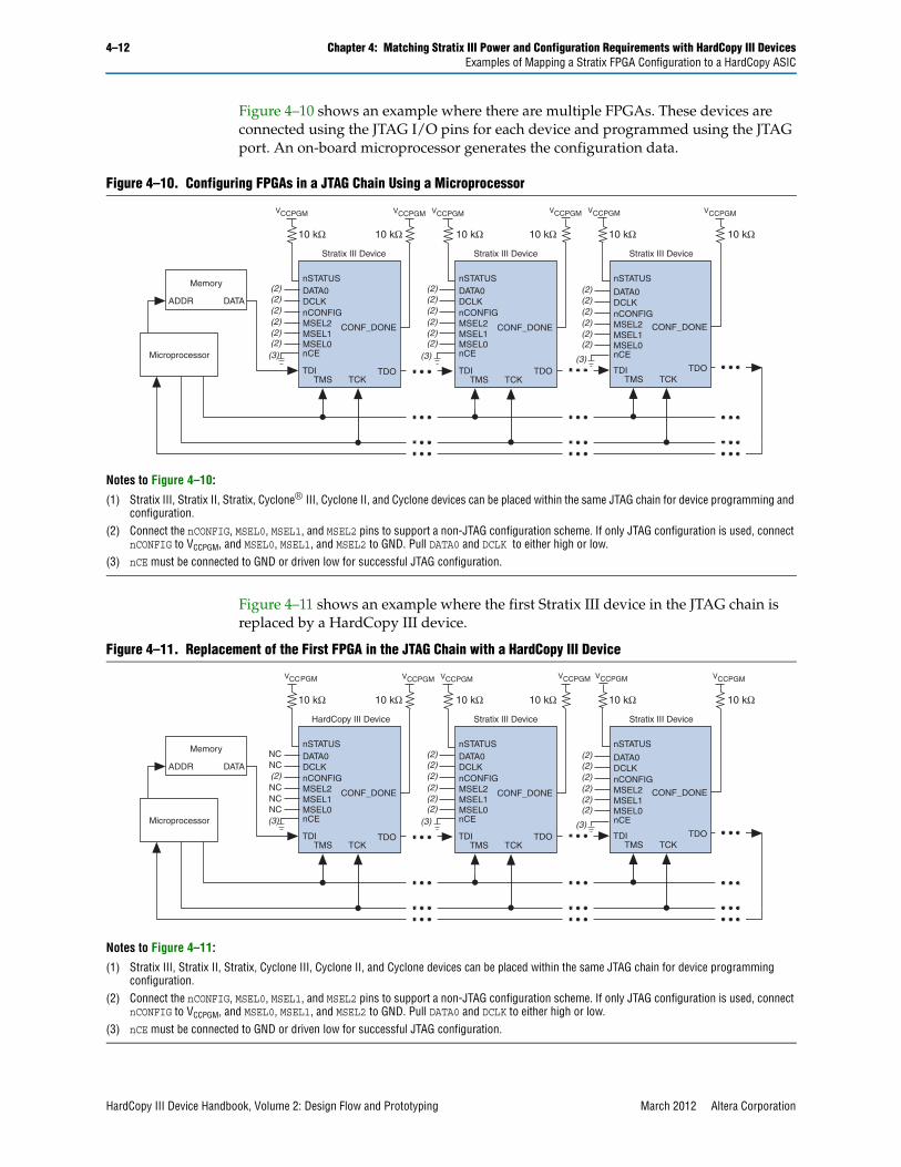
4–12 Chapter 4: Matching Stratix III Power and Configuration Requirements with HardCopy III DevicesExamples of Mapping a Stratix FPGA Configuration to a HardCopy ASIC
Figure 4–10 shows an example where there are multiple FPGAs. These devices are connected using the JTAG I/O pins for each device and programmed using the JTAG port. An on-board microprocessor generates the configuration data.
Figure 4–11 shows an example where the first Stratix III device in the JTAG chain is replaced by a HardCopy III device.
Figure 4–10. Configuring FPGAs in a JTAG Chain Using a Microprocessor
Notes to Figure 4–10:
(1) Stratix III, Stratix II, Stratix, Cyclone® III, Cyclone II, and Cyclone devices can be placed within the same JTAG chain for device programming and configuration.
(2) Connect the nCONFIG, MSEL0, MSEL1, and MSEL2 pins to support a non-JTAG configuration scheme. If only JTAG configuration is used, connect nCONFIG to VCCPGM, and MSEL0, MSEL1, and MSEL2 to GND. Pull DATA0 and DCLK to either high or low.
(3) nCE must be connected to GND or driven low for successful JTAG configuration.
TMS TCKTDI TDO
nSTATUS
nCONFIGMSEL2MSEL1
nCE
VCCPGM
CONF_DONE
VCCPGM
TMS TCKTDI TDO
nCONFIGMSEL2MSEL1
nCE
VCCPGM
CONF_DONE
VCCPGM
TMS TCKTDI TDO
nCONFIGMSEL2MSEL1
nCE
VCCPGM
CONF_DONE
VCCPGM
(2)(2)(2)
MSEL0(2)
(2)(2)(2)
MSEL0(2)
(2)DCLK DCLK DCLK(2)(2) (2)DATA0 DATA0 DATA0(2)(2) (2)
(2)(2)
MSEL0(2)
Stratix III Device Stratix III Device Stratix III Device
nSTATUS nSTATUS
10 kΩ 10 kΩ 10 kΩ10 kΩ10 kΩ10 kΩ
(3) (3) (3)
Memory
ADDR DATA
Microprocessor
Figure 4–11. Replacement of the First FPGA in the JTAG Chain with a HardCopy III Device
Notes to Figure 4–11:
(1) Stratix III, Stratix II, Stratix, Cyclone III, Cyclone II, and Cyclone devices can be placed within the same JTAG chain for device programming configuration.
(2) Connect the nCONFIG, MSEL0, MSEL1, and MSEL2 pins to support a non-JTAG configuration scheme. If only JTAG configuration is used, connect nCONFIG to VCCPGM, and MSEL0, MSEL1, and MSEL2 to GND. Pull DATA0 and DCLK to either high or low.
(3) nCE must be connected to GND or driven low for successful JTAG configuration.
TMS TCKTDI TDO
nSTATUS
nCONFIGMSEL2MSEL1
nCE
VCC
CONF_DONE
VCCPGM
TMS TCKTDI TDO
nCONFIGMSEL2MSEL1
nCE
VCCPGM
CONF_DONE
VCCPGM
TMS TCKTDI TDO
nCONFIGMSEL2MSEL1
nCE
VCCPGM
CONF_DONE
VCCPGM
(2)(2)(2)
MSEL0(2)
(2)
MSEL0
(2)DCLK DCLK DCLK(2) (2)DATA0 DATA0 DATA0(2)NC (2)
(2)(2)
MSEL0(2)
HardCopy III Device Stratix III Device Stratix III Device
nSTATUS nSTATUS
10 kΩ 10 kΩ 10 kΩ10 kΩ10 kΩ10 kΩ
(3) (3) (3)
Memory
ADDR DATA
Microprocessor
NC
NCNCNC
PGM
HardCopy III Device Handbook, Volume 2: Design Flow and Prototyping March 2012 Altera Corporation
Chapter 4: Matching Stratix III Power and Configuration Requirements with HardCopy III Devices 4–13Document Revision History
Document Revision HistoryTable 4–3 shows the revision history for this chapter.
Table 4–3. Document Revision History
Date Version Changes
March 2012 3.2 Updated ted nCEO Board Connection in Table 4–2.
January 2011 3.1 Added Table 4–1.
June 2009 3.0 Minor updates.
December 2008 2.0 Minor text edits.
May 2008 1.0 Initial release.
March 2012 Altera Corporation HardCopy III Device Handbook, Volume 2: Design Flow and Prototyping

4–14 Chapter 4: Matching Stratix III Power and Configuration Requirements with HardCopy III DevicesDocument Revision History
HardCopy III Device Handbook, Volume 2: Design Flow and Prototyping March 2012 Altera Corporation

March 2012 Altera Corporation
Additional Information
This chapter provides additional information about the document and Altera.
About this HandbookThis handbook provides comprehensive information about the Altera® HardCopy® IV family of devices.
How to Contact AlteraTo locate the most up-to-date information about Altera products, refer to the following table.
Typographic ConventionsThe following table shows the typographic conventions this document uses.
Contact (1) Contact Method Address
Technical support Website www.altera.com/support
Technical trainingWebsite www.altera.com/training
Email [email protected]
Product literature Website www.altera.com/literature
Non-technical support (General) Email [email protected]
(Software Licensing) Email [email protected]
Note to Table:
(1) You can also contact your local Altera sales office or sales representative.
Visual Cue Meaning
Bold Type with Initial Capital Letters
Indicate command names, dialog box titles, dialog box options, and other GUI labels. For example, Save As dialog box. For GUI elements, capitalization matches the GUI.
bold typeIndicates directory names, project names, disk drive names, file names, file name extensions, software utility names, and GUI labels. For example, \qdesigns directory, D: drive, and chiptrip.gdf file.
Italic Type with Initial Capital Letters Indicate document titles. For example, Stratix III Design Guidelines.
italic typeIndicates variables. For example, n + 1.
Variable names are enclosed in angle brackets (< >). For example, <file name> and <project name>.pof file.
Initial Capital Letters Indicate keyboard keys and menu names. For example, the Delete key and the Options menu.
“Subheading Title” Quotation marks indicate references to sections within a document and titles of Quartus II Help topics. For example, “Typographic Conventions.”
HardCopy III Device Handbook, Volume 2: Design Flow and Prototyping

Info–2 Additional InformationTypographic Conventions
Courier type
Indicates signal, port, register, bit, block, and primitive names. For example, data1, tdi, and input. The suffix n denotes an active-low signal. For example, resetn.
Indicates command line commands and anything that must be typed exactly as it appears. For example, c:\qdesigns\tutorial\chiptrip.gdf.
Also indicates sections of an actual file, such as a Report File, references to parts of files (for example, the AHDL keyword SUBDESIGN), and logic function names (for example, TRI).
r An angled arrow instructs you to press the Enter key.
1., 2., 3., anda., b., c., and so on
Numbered steps indicate a list of items when the sequence of the items is important, such as the steps listed in a procedure.
■ ■ ■ Bullets indicate a list of items when the sequence of the items is not important.
1 The hand points to information that requires special attention.
h A question mark directs you to a software help system with related information.
f The feet direct you to another document or website with related information.
c A caution calls attention to a condition or possible situation that can damage or destroy the product or your work.
w A warning calls attention to a condition or possible situation that can cause you injury.
The envelope links to the Email Subscription Management Center page of the Altera website, where you can sign up to receive update notifications for Altera documents.
Visual Cue Meaning
HardCopy III Device Handbook, Volume 2: Design Flow and Prototyping March 2012 Altera Corporation

101 Innovation DriveSan Jose, CA 95134www.altera.com
HC3_H5V3-3.3
Volume 3: Datasheet
HardCopy III Device Handbook,
HardCopy III Device Handbook, Volume 3: Datasheet

HardCopy III Device Handbook, Volume 3: Datasheet March 2012 Altera Corporation
© 2012 Altera Corporation. All rights reserved. ALTERA, ARRIA, CYCLONE, HARDCOPY, MAX, MEGACORE, NIOS, QUARTUS and STRATIX are Reg. U.S. Pat.& Tm. Off. and/or trademarks of Altera Corporation in the U.S. and other countries. All other trademarks and service marks are the property of their respectiveholders as described at www.altera.com/common/legal.html. Altera warrants performance of its semiconductor products to current specifications in accordancewith Altera’s standard warranty, but reserves the right to make changes to any products and services at any time without notice. Altera assumes no responsibility orliability arising out of the application or use of any information, product, or service described herein except as expressly agreed to in writing by Altera. Alteracustomers are advised to obtain the latest version of device specifications before relying on any published information and before placing orders for products orservices.
March 2012 Altera Corporation HardCopy III Device Handbook, Volume 3: Datasheet
Contents
Chapter Revision Dates . . . . . . . . . . . . . . . . . . . . . . . . . . . . . . . . . . . . . . . . . . . . . . . . . . . . . . . . . . . . . . . . . . . . . . . v
Section I. HardCopy III Device DatasheetRevision History . . . . . . . . . . . . . . . . . . . . . . . . . . . . . . . . . . . . . . . . . . . . . . . . . . . . . . . . . . . . . . . . . . . . . . . . 1–1
Chapter 1. DC and Switching Characteristics of HardCopy III DevicesElectrical Characteristics . . . . . . . . . . . . . . . . . . . . . . . . . . . . . . . . . . . . . . . . . . . . . . . . . . . . . . . . . . . . . . . . . 1–1
Operating Conditions . . . . . . . . . . . . . . . . . . . . . . . . . . . . . . . . . . . . . . . . . . . . . . . . . . . . . . . . . . . . . . . . . 1–1Absolute Maximum Ratings . . . . . . . . . . . . . . . . . . . . . . . . . . . . . . . . . . . . . . . . . . . . . . . . . . . . . . . . . 1–1Recommended Operating Conditions . . . . . . . . . . . . . . . . . . . . . . . . . . . . . . . . . . . . . . . . . . . . . . . . . 1–3DC Characteristics . . . . . . . . . . . . . . . . . . . . . . . . . . . . . . . . . . . . . . . . . . . . . . . . . . . . . . . . . . . . . . . . . . 1–4I/O Standard Specifications . . . . . . . . . . . . . . . . . . . . . . . . . . . . . . . . . . . . . . . . . . . . . . . . . . . . . . . . . . 1–8
Power Consumption . . . . . . . . . . . . . . . . . . . . . . . . . . . . . . . . . . . . . . . . . . . . . . . . . . . . . . . . . . . . . . . . . 1–11Switching Characteristics . . . . . . . . . . . . . . . . . . . . . . . . . . . . . . . . . . . . . . . . . . . . . . . . . . . . . . . . . . . . . . . . 1–11
Core Performance Specifications . . . . . . . . . . . . . . . . . . . . . . . . . . . . . . . . . . . . . . . . . . . . . . . . . . . . . . . 1–12Clock Tree Specifications . . . . . . . . . . . . . . . . . . . . . . . . . . . . . . . . . . . . . . . . . . . . . . . . . . . . . . . . . . . 1–12PLL Specifications . . . . . . . . . . . . . . . . . . . . . . . . . . . . . . . . . . . . . . . . . . . . . . . . . . . . . . . . . . . . . . . . . 1–12DSP Block Specifications . . . . . . . . . . . . . . . . . . . . . . . . . . . . . . . . . . . . . . . . . . . . . . . . . . . . . . . . . . . . 1–13TriMatrix Memory Block Specifications . . . . . . . . . . . . . . . . . . . . . . . . . . . . . . . . . . . . . . . . . . . . . . . 1–14JTAG Specifications . . . . . . . . . . . . . . . . . . . . . . . . . . . . . . . . . . . . . . . . . . . . . . . . . . . . . . . . . . . . . . . . 1–16
Periphery Performance . . . . . . . . . . . . . . . . . . . . . . . . . . . . . . . . . . . . . . . . . . . . . . . . . . . . . . . . . . . . . . . 1–17High-Speed I/O Specifications . . . . . . . . . . . . . . . . . . . . . . . . . . . . . . . . . . . . . . . . . . . . . . . . . . . . . . 1–17OCT Calibration Block Specifications . . . . . . . . . . . . . . . . . . . . . . . . . . . . . . . . . . . . . . . . . . . . . . . . . 1–19Duty Cycle Distortion (DCD) Specifications . . . . . . . . . . . . . . . . . . . . . . . . . . . . . . . . . . . . . . . . . . . 1–19
Glossary . . . . . . . . . . . . . . . . . . . . . . . . . . . . . . . . . . . . . . . . . . . . . . . . . . . . . . . . . . . . . . . . . . . . . . . . . . . . . . 1–19Document Revision History . . . . . . . . . . . . . . . . . . . . . . . . . . . . . . . . . . . . . . . . . . . . . . . . . . . . . . . . . . . . . 1–23
Chapter 2. Extended Temperature Range for HardCopy III DevicesExtended Temperature Support . . . . . . . . . . . . . . . . . . . . . . . . . . . . . . . . . . . . . . . . . . . . . . . . . . . . . . . . . . . 2–1
Software Support . . . . . . . . . . . . . . . . . . . . . . . . . . . . . . . . . . . . . . . . . . . . . . . . . . . . . . . . . . . . . . . . . . . . . 2–2Limitations to Datasheet Specifications . . . . . . . . . . . . . . . . . . . . . . . . . . . . . . . . . . . . . . . . . . . . . . . . . . . . . 2–2
DSP Block Specifications . . . . . . . . . . . . . . . . . . . . . . . . . . . . . . . . . . . . . . . . . . . . . . . . . . . . . . . . . . . . . . . 2–2TriMatrix Memory Block Specifications . . . . . . . . . . . . . . . . . . . . . . . . . . . . . . . . . . . . . . . . . . . . . . . . . . 2–3Transceiver Performance Specifications . . . . . . . . . . . . . . . . . . . . . . . . . . . . . . . . . . . . . . . . . . . . . . . . . . 2–4
Document Revision History . . . . . . . . . . . . . . . . . . . . . . . . . . . . . . . . . . . . . . . . . . . . . . . . . . . . . . . . . . . . . . 2–4
Additional InformationHow to Contact Altera . . . . . . . . . . . . . . . . . . . . . . . . . . . . . . . . . . . . . . . . . . . . . . . . . . . . . . . . . . . . . . . . Info–1Typographic Conventions . . . . . . . . . . . . . . . . . . . . . . . . . . . . . . . . . . . . . . . . . . . . . . . . . . . . . . . . . . . . . Info–1

iv Contents
HardCopy III Device Handbook, Volume 3: Datasheet March 2012 Altera Corporation

March 2012 Altera Corporation HardCopy III Device Handbook, Volume 3: Datasheet
Chapter Revision Dates
The chapters in this document, HardCopy III Device Handbook, Volume 3: Datasheet, were revised on the following dates. Where chapters or groups of chapters are available separately, part numbers are listed.
Chapter 1. DC and Switching Characteristics of HardCopy III DevicesRevised: December 2011Part Number: HIII52001-4.1
Chapter 2. Extended Temperature Range for HardCopy III DevicesRevised: March 2012Part Number: HIII52002-1.0

vi Chapter Revision Dates
HardCopy III Device Handbook, Volume 3: Datasheet March 2012 Altera Corporation

March 2012 Altera Corporation HardCopy III Device Handbook, Volume 3: Datasheet
Section I. HardCopy III Device Datasheet
This section provides the datasheet for the HardCopy® III device family. This section includes the following chapter:
■ Chapter 1, DC and Switching Characteristics of HardCopy III Devices
■ Chapter 2, Extended Temperature Range for HardCopy III Devices
Revision HistoryRefer to each chapter for its own specific revision history. For information on when each chapter was updated, refer to the Chapter Revision Dates section, which appears in the full handbook.

I–2 Section I: HardCopy III Device DatasheetRevision History
HardCopy III Device Handbook, Volume 3: Datasheet March 2012 Altera Corporation

HardCopy III Device Handbook, Volume 3December 2011
HIII52001-4.1
Subscribe
© 2011 Altera Corporation. All rights reserved. ALTERA, ARRIA, CYCLONE, HARDCOPY, MAX, MEGACORE, NIOS, QUARTUS and STRATIX are Reg. U.S. Pat. & Tm. Off. and/or trademarks of Altera Corporation in the U.S. and other countries. All other trademarks and service marks are the property of their respective holders as described at www.altera.com/common/legal.html. Altera warrants performance of its semiconductor products to current specifications in accordance with Altera’s standard warranty, but reserves the right to make changes to any products and services at any time without notice. Altera assumes no responsibility or liability arising out of the application or use of any information, product, or service described herein except as expressly agreed to in writing by Altera. Altera customers are advised to obtain the latest version of device specifications before relying on any published information and before placing orders for products or services.
1. DC and Switching Characteristics ofHardCopy III Devices
Electrical CharacteristicsThis chapter provides information about the absolute maximum ratings, recommended operating conditions, DC electrical characteristics, and other specifications for HardCopy® III devices.
Operating ConditionsWhen implementing HardCopy III devices in a system, the system rates the devices according to a set of defined parameters. To maintain the highest performance and reliability, you must consider the operating requirements described in this chapter. HardCopy III devices are not speed binned because HardCopy III devices function at a target frequency based on timing constraints, and operate at either commercial or industrial temperatures.
Absolute Maximum RatingsAbsolute maximum ratings define the maximum operating conditions for HardCopy III devices. Experiments with the device and theoretical modeling of breakdown and damage mechanisms provide these values.
Table 1–1 lists the absolute maximum ratings for a HardCopy III device.
1 Conditions beyond those listed in Table 1–1 can cause permanent damage to the device. Additionally, device operation at the absolute maximum ratings for extended periods of time can have adverse effects on the device.
Table 1–1. HardCopy III Device Absolute Maximum Ratings (Part 1 of 2) (Note 1)
Symbol Parameter Minimum Maximum Unit
VCCL Core voltage power supply –0.5 1.35 V
VCC I/O registers power supply –0.5 1.35 V
VCCD_PLL PLL digital power supply –0.5 1.35 V
VCCA_PLL PLL analog power supply –0.5 3.75 V
VCCPT (2) Power supply for the temperature sensing diode
–0.5 3.75 V
VCCPGM Configuration pins power supply –0.5 3.9 V
VCCPD I/O predriver power supply –0.5 3.9 V
VCCIO I/O power supply –0.5 3.9 V
VCC_CLKINDifferential clock input power supply (top and bottom I/O banks only)
–0.5 3.75 V
VCCBAT (3) Battery back-up power supply for design security volatile key register
— — V
December 2011HIII52001-4.1

1–2 Chapter 1: DC and Switching Characteristics of HardCopy III DevicesElectrical Characteristics
HardCopy III Device Handbook, Volume 3 December 2011 Altera Corporation
Maximum Allowed Overshoot and Undershoot Voltage
During transitions, input signals may overshoot to the voltage shown in Table 1–2 and undershoot to –2.0 V for input currents less than 100 mA and periods shorter than 20 ns.
Table 1–2 lists the maximum allowed input overshoot voltage. The maximum allowed overshoot duration is the percentage of high time over the lifetime of the device. A DC signal is equivalent to 100% duty cycle.
VI DC input voltage –0.5 4.0 V
TJ Operating junction temperature –55 125 °C
IOUT DC output current, per pin –25 40 mA
TSTG Storage temperature (no bias) –65 150 °C
Notes to Table 1–1:
(1) Supply voltage specifications apply to voltage readings taken at the device pins and not the power supply.(2) Stratix III devices use this power supply for programmable power technology.(3) HardCopy III devices do not use this power supply.
Table 1–1. HardCopy III Device Absolute Maximum Ratings (Part 2 of 2) (Note 1)
Symbol Parameter Minimum Maximum Unit
Table 1–2. Maximum Allowed Overshoot During Transitions
Symbol Parameter ConditionOvershoot
Duration as % of High Time
Unit
Vi (AC) AC Input Voltage
4 100.000 %
4.05 79.330 %
4.1 46.270 %
4.15 27.030 %
4.2 15.800 %
4.25 9.240 %
4.3 5.410 %
4.35 3.160 %
4.4 1.850 %
4.45 1.080 %
4.5 0.630 %
4.55 0.370 %
4.6 0.220 %
4.65 0.130 %
4.7 0.074 %
4.75 0.043 %
4.8 0.025 %
4.85 0.015 %
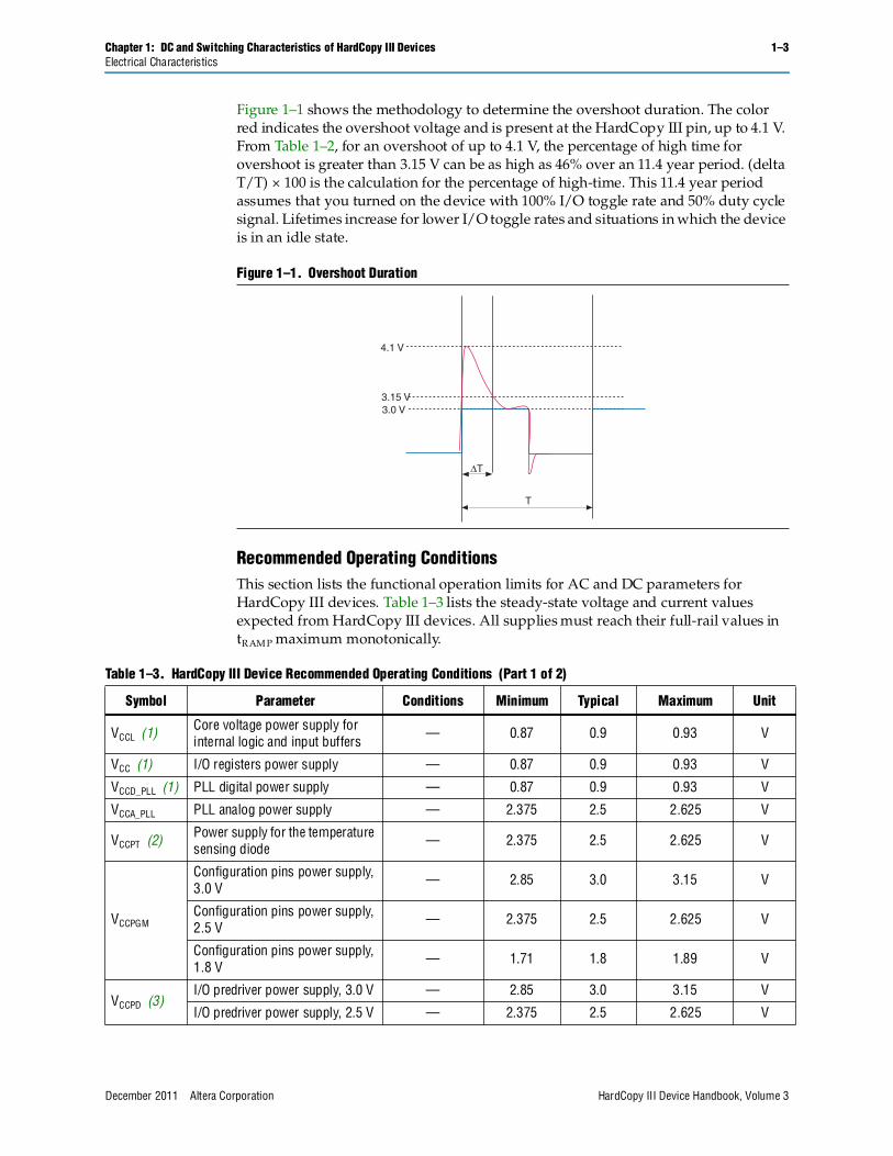
Chapter 1: DC and Switching Characteristics of HardCopy III Devices 1–3Electrical Characteristics
December 2011 Altera Corporation HardCopy III Device Handbook, Volume 3
Figure 1–1 shows the methodology to determine the overshoot duration. The color red indicates the overshoot voltage and is present at the HardCopy III pin, up to 4.1 V. From Table 1–2, for an overshoot of up to 4.1 V, the percentage of high time for overshoot is greater than 3.15 V can be as high as 46% over an 11.4 year period. (delta T/T) × 100 is the calculation for the percentage of high-time. This 11.4 year period assumes that you turned on the device with 100% I/O toggle rate and 50% duty cycle signal. Lifetimes increase for lower I/O toggle rates and situations in which the device is in an idle state.
Recommended Operating ConditionsThis section lists the functional operation limits for AC and DC parameters for HardCopy III devices. Table 1–3 lists the steady-state voltage and current values expected from HardCopy III devices. All supplies must reach their full-rail values in tRAM P maximum monotonically.
Figure 1–1. Overshoot Duration
3.0 V3.15 V
4.1 V
T
ΔT
Table 1–3. HardCopy III Device Recommended Operating Conditions (Part 1 of 2)
Symbol Parameter Conditions Minimum Typical Maximum Unit
VCCL (1) Core voltage power supply for internal logic and input buffers
— 0.87 0.9 0.93 V
VCC (1) I/O registers power supply — 0.87 0.9 0.93 V
VCCD_PLL (1) PLL digital power supply — 0.87 0.9 0.93 V
VCCA_PLL PLL analog power supply — 2.375 2.5 2.625 V
VCCPT (2) Power supply for the temperature sensing diode
— 2.375 2.5 2.625 V
VCCPGM
Configuration pins power supply, 3.0 V
— 2.85 3.0 3.15 V
Configuration pins power supply, 2.5 V
— 2.375 2.5 2.625 V
Configuration pins power supply, 1.8 V
— 1.71 1.8 1.89 V
VCCPD (3)I/O predriver power supply, 3.0 V — 2.85 3.0 3.15 V
I/O predriver power supply, 2.5 V — 2.375 2.5 2.625 V
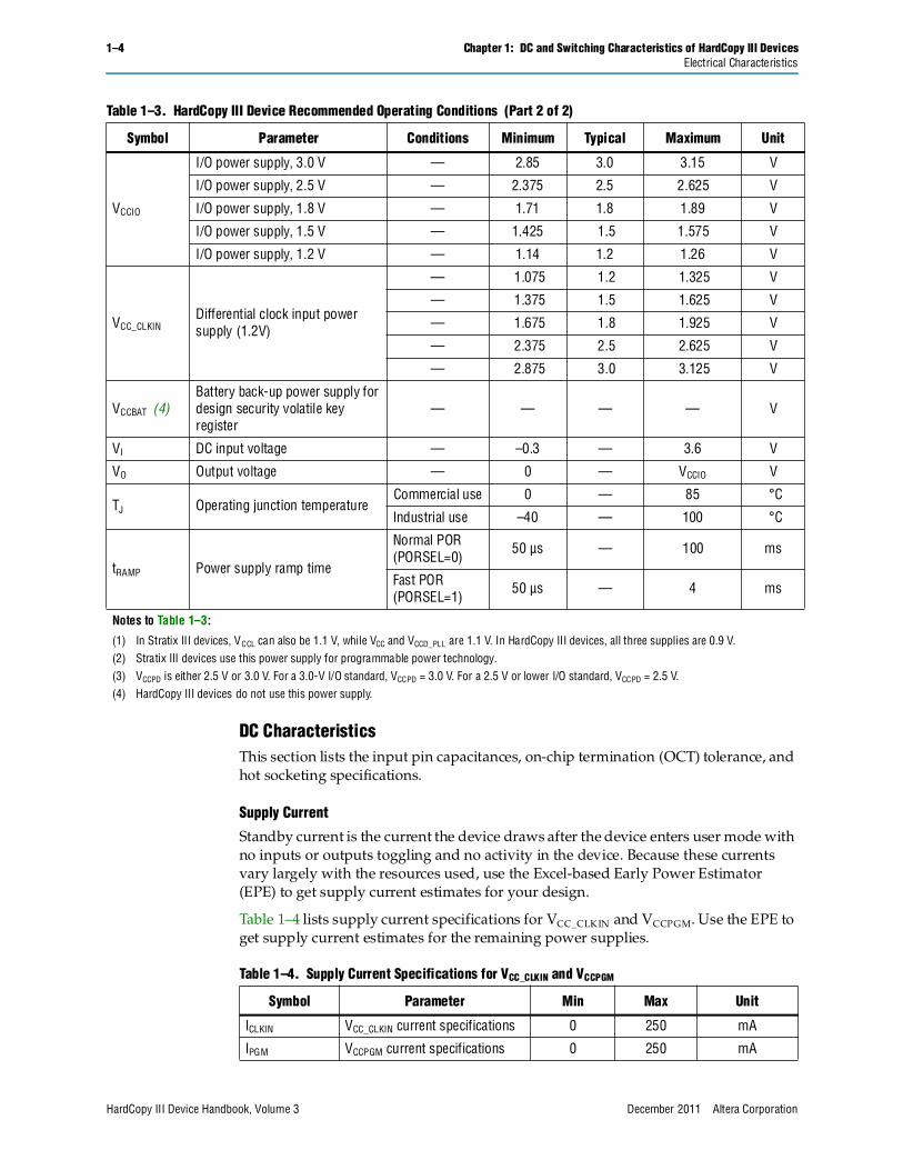
1–4 Chapter 1: DC and Switching Characteristics of HardCopy III DevicesElectrical Characteristics
HardCopy III Device Handbook, Volume 3 December 2011 Altera Corporation
DC CharacteristicsThis section lists the input pin capacitances, on-chip termination (OCT) tolerance, and hot socketing specifications.
Supply Current
Standby current is the current the device draws after the device enters user mode with no inputs or outputs toggling and no activity in the device. Because these currents vary largely with the resources used, use the Excel-based Early Power Estimator (EPE) to get supply current estimates for your design.
Table 1–4 lists supply current specifications for VCC_CLKIN and VCCPGM. Use the EPE to get supply current estimates for the remaining power supplies.
VCCIO
I/O power supply, 3.0 V — 2.85 3.0 3.15 V
I/O power supply, 2.5 V — 2.375 2.5 2.625 V
I/O power supply, 1.8 V — 1.71 1.8 1.89 V
I/O power supply, 1.5 V — 1.425 1.5 1.575 V
I/O power supply, 1.2 V — 1.14 1.2 1.26 V
VCC_CLKINDifferential clock input power supply (1.2V)
— 1.075 1.2 1.325 V
— 1.375 1.5 1.625 V
— 1.675 1.8 1.925 V
— 2.375 2.5 2.625 V
— 2.875 3.0 3.125 V
VCCBAT (4)Battery back-up power supply for design security volatile key register
— — — — V
VI DC input voltage — –0.3 — 3.6 V
VO Output voltage — 0 — VCCIO V
TJ Operating junction temperatureCommercial use 0 — 85 °C
Industrial use –40 — 100 °C
tRAMP Power supply ramp time
Normal POR (PORSEL=0)
50 µs — 100 ms
Fast POR (PORSEL=1)
50 µs — 4 ms
Notes to Table 1–3:
(1) In Stratix III devices, VCCL can also be 1.1 V, while VCC and VCCD_PLL are 1.1 V. In HardCopy III devices, all three supplies are 0.9 V.(2) Stratix III devices use this power supply for programmable power technology.(3) VCCPD is either 2.5 V or 3.0 V. For a 3.0-V I/O standard, VCCPD = 3.0 V. For a 2.5 V or lower I/O standard, VCCPD = 2.5 V.(4) HardCopy III devices do not use this power supply.
Table 1–3. HardCopy III Device Recommended Operating Conditions (Part 2 of 2)
Symbol Parameter Conditions Minimum Typical Maximum Unit
Table 1–4. Supply Current Specifications for VCC_CLKIN and VCCPGM
Symbol Parameter Min Max Unit
ICLKIN VCC_CLKIN current specifications 0 250 mA
IPGM VCCPGM current specifications 0 250 mA

Chapter 1: DC and Switching Characteristics of HardCopy III Devices 1–5Electrical Characteristics
December 2011 Altera Corporation HardCopy III Device Handbook, Volume 3
I/O Pin Leakage Current
Table 1–5 lists HardCopy III I/O pin leakage current specifications.
Bus Hold Specifications
Table 1–6 lists the HardCopy III bus hold specifications.
OCT Specifications
If you enabled OCT calibration, calibration is automatically performed at power up for I/Os connected to the calibration block. Table 1–7 lists the HardCopy III OCT calibration block accuracy specifications.
Table 1–5. HardCopy III I/O Pin Leakage Current (Note 1), (2)
Symbol Parameter Conditions Min Typ Max Unit
II Input pin leakage current VI = VCCIOMAX to 0 V –20 — 20 μA
IOZTri-stated I/O pin leakage current
VO = VCCIOMAX to 0 V –20 — 20 μA
Notes To Table 1–5:
(1) This value is for normal device operation. The value may vary during power up. This applies for all VCCIO settings (3.0, 2.5, 1.8, 1.5, and 1.2 V).
(2) The 20 mA I/O leakage current limit is applicable when the internal clamping diode is off. You can observe a higher current when the diode is on.
Table 1–6. Bus Hold Parameters
Parameter Symbol Condition
VCCIO
Unit1.2 V 1.5 V 1.8 V 2.5 V 3.0 V
Min Max Max Min Max Min Min Max Max Max
Low sustaining current
ISUSLVIN > VIL
(maximum)22.5 — 25.0 — 30.0 — 50.0 — 70.0 — μA
High sustaining current
ISUSHVIN < VIH
(minimum)–22.5 — –25.0 — –30.0 — –50.0 — –70.0 — μA
Low overdrive current
IODL 0V < VIN < VCCIO — 120 — 160 — 200 — 300 — 500 μA
High overdrive current
IODH 0V < VIN < VCCIO — –120 — –160 — –200 — –300 — –500 μA
Bus-hold trip point
VTRIP — 0.45 0.95 0.50 1.00 0.68 1.07 0.70 1.70 0.80 2.00 V
Table 1–7. HardCopy III OCT Calibration Accuracy Specifications (Part 1 of 2) (Note 1)
Symbol Description Conditions Calibration Accuracy Unit
25-Ω RS 3.0/2.5/1.8/1.5/1.2 (2) Internal series termination with calibration (25-Ω setting)
VCCIO = 3.0/2.5/1.8/1.5/1.2 V ±8 %
50-Ω RS 3.0/2.5/1.8/1.5/1.2 Internal series termination with calibration (50-Ω setting)
VCCIO = 3.0/2.5/1.8/1.5/1.2 V ±8 %

1–6 Chapter 1: DC and Switching Characteristics of HardCopy III DevicesElectrical Characteristics
HardCopy III Device Handbook, Volume 3 December 2011 Altera Corporation
The accuracy listed in Table 1–7 is valid at the time of calibration. If the voltage or temperature changes, the termination resistance value varies. Table 1–8 lists the resistance tolerance for HardCopy III on-chip termination.
Table 1–9 lists OCT variation with temperature and voltage after power-up calibration.
1 The RCAL is calibrated OCT at power-up. ΔT and ΔV are variations in temperature and voltage (VCCIO) at power-up.
50-Ω RT 2.5/1.8/1.5/1.2 Internal parallel termination with calibration (50-Ω setting)
VCCIO = 2.5/1.8/1.5/1.2 V ±10 %
25-Ω, 25-Ω, and 25-Ω RS 3.0/2.5/1.8/1.5/1.2 (3)
Expanded range for internal series termination with calibration (20-Ω, 40-Ω and 60-Ω RS settings)
VCCIO = 3.0/2.5/1.8/1.5/1.2 V ±10 %
25-Ω RS_left_shift
Internal left shift series termination with calibration (25-Ω RS_left_shift setting)
VCCIO = 3.0/2.5/1.8/1.5/1.2 V ±10 %
Notes to Table 1–7:
(1) OCT calibration accuracy is valid at the time of calibration only.(2) 25-Ω RS not supported for 1.5 V and 1.2 V in Row I/O.(3) 20-Ω RS not supported for 1.5 V and 1.2 V in Row I/O.
Table 1–7. HardCopy III OCT Calibration Accuracy Specifications (Part 2 of 2) (Note 1)
Symbol Description Conditions Calibration Accuracy Unit
Table 1–8. OCT Resistance Tolerance Specification for I/Os
Symbol Description Conditions Resistance Tolerance Unit
25-Ω RS 3.0/2.5 Internal series termination without calibration (25-Ω setting) VCCIO = 3.0/2.5 V ±40 %
25-Ω RS 1.8/1.5 Internal series termination without calibration (25-Ω setting) VCCIO = 1.8/1.5 V ±40 %
25-Ω RS 1.2 Internal series termination without calibration (25-Ω setting) VCCIO = 1.2 V ±50 %
50-Ω RS 3.0/2.5 Internal series termination without calibration (50-Ω setting) VCCIO = 3.0/2.5 V ±40 %
50-Ω RS 1.8/1.5 Internal series termination without calibration (50-Ω setting) VCCIO = 1.8/1.5 V ±40 %
50-Ω RS 1.2 Internal series termination without calibration (50-Ω setting) VCCIO = 1.2 V ±50 %
Table 1–9. OCT Variation after Power-up Calibration (Part 1 of 2) (Note 1)
Symbol Description VCCIO (V) Commercial Typical Unit
dR/dV OCT variation with voltage without recalibration
3.0 0.0297 %/mV
2.5 0.0344 %/mV
1.8 0.0499 %/mV
1.5 0.0744 %/mV
1.2 0.1241 %/mV
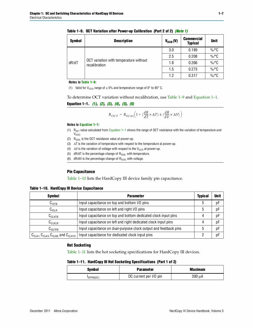
Chapter 1: DC and Switching Characteristics of HardCopy III Devices 1–7Electrical Characteristics
December 2011 Altera Corporation HardCopy III Device Handbook, Volume 3
To determine OCT variation without recalibration, use Table 1–9 and Equation 1–1.
Pin Capacitance
Table 1–10 lists the HardCopy III device family pin capacitance.
Hot Socketing
Table 1–11 lists the hot socketing specifications for HardCopy III devices.
dR/dTOCT variation with temperature without recalibration
3.0 0.189 %/°C
2.5 0.208 %/°C
1.8 0.266 %/°C
1.5 0.273 %/°C
1.2 0.317 %/°C
Notes to Table 1–9:
(1) Valid for VCCIO range of ± 5% and temperature range of 0° to 85° C.
Equation 1–1. (1), (2), (3), (4), (5), (6)
Notes to Equation 1–1:(1) ROCT value calculated from Equation 1–1 shows the range of OCT resistance with the variation of temperature and
VCCIO.(2) RSCAL is the OCT resistance value at power-up. (3) ΔT is the variation of temperature with respect to the temperature at power-up.(4) ΔV is the variation of voltage with respect to the VCCIO at power-up. (5) dR/dT is the percentage change of RSCAL with temperature.(6) dR/dV is the percentage change of RSCAL with voltage.
Table 1–9. OCT Variation after Power-up Calibration (Part 2 of 2) (Note 1)
Symbol Description VCCIO (V) Commercial Typical Unit
ROCT RSCA L 1 dRdT------- ΔT× dR
dV------- ΔV× ±+
=
Table 1–10. HardCopy III Device Capacitance
Symbol Parameter Typical Unit
CIOTB Input capacitance on top and bottom I/O pins 5 pF
CIOLR Input capacitance on left and right I/O pins 5 pF
CCLKTB Input capacitance on top and bottom dedicated clock input pins 4 pF
CCLKLR Input capacitance on left and right dedicated clock input pins 4 pF
COUTFB Input capacitance on dual-purpose clock output and feedback pins 5 pF
CCLK1, CCLK3, CCLK8, and CCLK10 Input capacitance for dedicated clock input pins 2 pF
Table 1–11. HardCopy III Hot Socketing Specifications (Part 1 of 2)
Symbol Parameter Maximum
IIOPIN(DC) DC current per I/O pin 300 μA

1–8 Chapter 1: DC and Switching Characteristics of HardCopy III DevicesElectrical Characteristics
HardCopy III Device Handbook, Volume 3 December 2011 Altera Corporation
Internal Weak Pull-Up Resistor
Table 1–12 lists the weak pull-up resistor values for HardCopy III devices.
I/O Standard SpecificationsTable 1–13 through Table 1–18 list input voltage sensitivities (VIH and VIL), output voltage (VOH and VOL), and current drive characteristics (IOH and IOL) for all I/O standards supported by HardCopy III devices. For an explanation of terms used in Table 1–13 through Table 1–18, refer to Table 1–30 on page 1–19. VOL and VOH values are valid at the corresponding IOL and IOH, respectively.
IIOPIN(AC) AC current per I/O pin 8 mA (1)
Note to Table 1–11:
(1) The I/O ramp rate is 10 ns or more. For ramp rates faster than 10 ns, |IIOPIN| = Cdv/dt, in which C is I/O pin capacitance and dv/dt is the slew rate.
Table 1–11. HardCopy III Hot Socketing Specifications (Part 2 of 2)
Symbol Parameter Maximum
Table 1–12. HardCopy III Internal Weak Pull-Up Resistor (Note 1), (2)
Symbol Parameter Conditions Typ Unit
RPU
Value of I/O pin pull-up resistor before and during configuration, as well as user mode if the programmable pull-up resistor option is enabled
VCCIO = 3.0 V ± 5% (3) 25 kΩ
VCCIO = 2.5 V ± 5% (3) 25 kΩ
VCCIO = 1.8 V ± 5% (3) 25 kΩ
VCCIO = 1.5 V ± 5% (3) 25 kΩ
VCCIO = 1.2 V ± 5% (3) 25 kΩ
Notes to Table 1–12:
(1) All I/O pins have an option to enable weak pull-up except test and JTAG pins.(2) The internal weak pull-down feature is only available for JTAG TCK pin. The typical value for this internal weak pull-down resistor is around 25k.(3) Pin pull-up resistance values may be lower if an external source drives the pin higher than VCCIO.
Table 1–13. Single-Ended I/O Standards Specifications
I/O StandardVCCIO (V) VIL (V) VIH (V) VOL (V) VOH (V)
IOL (mA) IOH (mA)Min Typ Max Min Max Min Max Max Min
3.3-V LVTTL 2.85 3 3.15 –0.3 0.8 1.7 3.6 0.4 2.4 2 –2
3.3-V LVCMOS 2.85 3 3.15 –0.3 0.8 1.7 3.6 0.2VCCIO –
0.20.1 –0.1
2.5-V LVTTL/ LVCMOS
2.375
2.5 2.625 –0.3 0.7 1.7 3.6 0.2 2.1 0.1 –0.1
2.5 2.625 –0.3 0.7 1.7 3.6 0.4 2 1 –1
2.5 2.625 –0.3 0.7 1.7 3.6 0.7 1.7 2 –2
1.8-V LVTTL/ LVCMOS
1.71 1.8 1.89 –0.30.35 × VCCIO
0.65 × VCCIO
VCCIO + 0.3
0.45VCCIO – 0.45
2 –2
1.5-V LVTTL/ LVCMOS
1.425 1.5 1.575 –0.30.35 × VCCIO
0.65 × VCCIO
VCCIO + 0.3
0.25 × VCCIO
0.75 × VCCIO
2 –2
1.2-V LVTTL/ LVCMOS
1.14 1.2 1.26 –0.30.35 × VCCIO
0.65 × VCCIO
VCCIO + 0.3
0.25 × VCCIO
0.75 × VCCIO
2 –2

Chapter 1: DC and Switching Characteristics of HardCopy III Devices 1–9Electrical Characteristics
December 2011 Altera Corporation HardCopy III Device Handbook, Volume 3
For an example of a voltage referenced receiver input waveform and an explanation of terms used in Table 1–14, refer to Figure 1–6 on page 1–21.
3.0-V PCI 2.85 3 3.15 —0.3 × VCCIO
0.5 × VCCIO
3.60.1 × VCCIO
0.9 × VCCIO
1.5 –0.5
3.0-V PCI-X 2.85 3 3.15 —0.35 × VCCIO
0.5 × VCCIO
—0.1 × VCCIO
0.9 × VCCIO
1.5 –0.5
Table 1–13. Single-Ended I/O Standards Specifications
I/O StandardVCCIO (V) VIL (V) VIH (V) VOL (V) VOH (V)
IOL (mA) IOH (mA)Min Typ Max Min Max Min Max Max Min
Table 1–14. Single-Ended SSTL and HSTL I/O Reference Voltage Specifications
I/O StandardVCCIO (V) VREF (V) VTT (V)
Min Typ Max Min Typ Max Min Typ Max
SSTL-2 CLASS I, II 2.375 2.5 2.6250.49 × VCCIO
0.5 × VCCIO0.51 × VCCIO
VREF – 0.04
VREFVREF + 0.04
SSTL-18 CLASS I, II 1.71 1.8 1.89 0.833 0.9 0.969 VREF – 0.04
VREFVREF + 0.04
SSTL-15 CLASS I, II 1.425 1.5 1.5750.47 × VCCIO
0.5 × VCCIO0.53 × VCCIO
0.47 × VCCIO
VREF0.53 × VCCIO
HSTL-18 CLASS I, II 1.71 1.8 1.89 0.85 0.9 0.95 — VCCIO/2 —
HSTL-15 CLASS I, II 1.425 1.5 1.575 0.68 0.75 0.9 — VCCIO/2 —
HSTL-12 CLASS I, II 1.14 1.2 1.260.47 × VCCIO
0.5 × VCCIO0.53 × VCCIO
— VCCIO/2 —
Table 1–15. Single-Ended SSTL and HSTL I/O Standards Signal Specifications (Part 1 of 2)
I/O StandardVIL(DC) (V) VIH(DC) (V) VIL(AC)
(V)VIH(AC)
(V) VOL (V) VOH (V)IOL (mA) IOH (mA)
Min Max Min Max Max Min Max Min
SSTL-2 CLASS I –0.3VREF – 0.15
VREF + 0.15
VCCIO + 0.3
VREF – 0.31
VREF + 0.31
VTT – 0.57
VTT + 0.57
8.1 –8.1
SSTL-2 CLASS II –0.3VREF – 0.15
VREF + 0.15
VCCIO + 0.3
VREF – 0.31
VREF + 0.31
VTT – 0.76
VTT + 0.76
16.2 –16.2
SSTL-18 CLASS I –0.3VREF – 0.125
VREF + 0.125
VCCIO + 0.3
VREF – 0.25
VREF + 0.25
VTT – 0.475
VTT + 0.475
6.7 –6.7
SSTL-18 CLASS II –0.3VREF – 0.125
VREF + 0.125
VCCIO + 0.3
VREF – 0.25
VREF + 0.25
0.28VCCIO – 0.28
13.4 –13.4
SSTL-15 CLASS I –0.3 VREF – 0.1 VREF + 0.1VCCIO +
0.3VREF – 0.175
VREF + 0.175
0.2 × VCCIO
0.8 × VCCIO
8 –8
SSTL-15 CLASS II –0.3 VREF – 0.1 VREF + 0.1VCCIO +
0.3VREF – 0.175
VREF + 0.175
0.2 × VCCIO
0.8 × VCCIO
16 –16
HSTL-18 CLASS I –0.3 VREF – 0.1 VREF + 0.1VCCIO +
0.3VREF – 0.2 VREF + 0.2 0.4
VCCIO – 0.4
8 –8
HSTL-18 CLASS II –0.3 VREF – 0.1 VREF + 0.1VCCIO +
0.3VREF – 0.2 VREF + 0.2 0.4
VCCIO – 0.4
16 –16
HSTL-15 CLASS I –0.3 VREF – 0.1 VREF + 0.1VCCIO +
0.3VREF – 0.2 VREF + 0.2 0.4
VCCIO – 0.4
8 –8

1–10 Chapter 1: DC and Switching Characteristics of HardCopy III DevicesElectrical Characteristics
HardCopy III Device Handbook, Volume 3 December 2011 Altera Corporation
For receiver input and transmitter output waveforms, and for all differential I/O standards (LVDS, mini-LVDS, RSDS), refer to Figure 1–2 on page 1–20. VCC_CLKIN is the power supply for differential column clock input pins. VCCPD is the power supply for row I/Os and all other column I/Os.
HSTL-15 CLASS II –0.3 VREF – 0.1 VREF + 0.1VCCIO +
0.3VREF – 0.2 VREF + 0.2 0.4
VCCIO – 0.4
16 –16
HSTL-12 CLASS I –0.15VREF – 0.08
VREF + 0.08
VCCIO + 0.15
VREF – 0.15
VREF + 0.15
0.25 × VCCIO
0.75 × VCCIO
8 –8
HSTL-12 CLASS II –0.15VREF – 0.08
VREF + 0.08
VCCIO + 0.15
VREF – 0.15
VREF + 0.15
0.25 × VCCIO
0.75 × VCCIO
16 –16
Table 1–15. Single-Ended SSTL and HSTL I/O Standards Signal Specifications (Part 2 of 2)
I/O StandardVIL(DC) (V) VIH(DC) (V) VIL(AC)
(V)VIH(AC)
(V) VOL (V) VOH (V)IOL (mA) IOH (mA)
Min Max Min Max Max Min Max Min
Table 1–16. Differential SSTL I/O Standard Specifications
I/O StandardVCCIO (V) VSWING (DC) (V) VX (AC) (V) VSWING (AC) (V) VOX (AC) (V)
Min Typ Max Min Max Min Typ Max Min Max Min Typ Max
SSTL-2 CLASS I, CLASS II
2.375 2.5 2.625 0.3VCCIO +
0.6VCCIO/2 – 0.2
—VCCIO/2 + 0.2
0.6VCCIO
+ 0.6VCCIO/2 – 0.15
—VCCIO/2 + 0.15
SSTL-18 CLASS I, CLASS II
1.71 1.8 1.89 0.3VCCIO +
0.6
VCCIO/2 –
0.175—
VCCIO/2 +
0.1750.5
VCCIO
+ 0.6
VCCIO/2 –
0.125—
VCCIO/2 +
0.125
SSTL-15 CLASS I, CLASS II
1.425 1.5 1.575 0.2 — — VCCIO/2 — 0.4 — — VCCIO/2 —
Table 1–17. Differential HSTL I/O Standards Specifications
I/O StandardVCCIO (V) VDIF(DC) (V) VX(AC) (V) VCM(DC) (V) VDIF(AC) (V)
Min Typ Max Min Max Min Typ Max Min Typ Max Min Max
HSTL-18 CLASS I, II
1.71 1.8 1.89 0.2 — 0.78 — 1.12 0.78 — 1.12 0.4 —
HSTL-15 CLASS I, II
1.425 1.5 1.575 0.2 — 0.68 — 0.9 0.68 — 0.9 0.4 —
HSTL-12 CLASS I, II
1.14 1.2 1.26 0.16VCCIO +
0.3—
0.5 × VCCIO
—0.4 × VCCIO
0.5 × VCCIO
0.6 × VCCIO
0.3VCCIO + 0.48
Table 1–18. Differential I/O Standard Specifications (Note 1) (Part 1 of 2)
I/O Standard
VCCIO (V) VID (mV) VICM(DC) (V) VOD (V) (2) VOCM (V) (2)
Min Typ Max Min Condition Max Min Condition Max Min Typ Max Min Typ Max
2.5-V LVDS (HIO)
2.375 2.5 2.625 100 VCM = 1.25V— 0.05
Dmax ≤ 700 Mbps
1.8 0.247 — 0.6 1.125 1.25 1.375
— 1.05Dmax >
700 Mbps1.55 0.247 — 0.6 1.125 1.25 1.375
2.5-V LVDS (VIO)
2.375 2.5 2.625 100 VCM = 1.25V— 0.05
Dmax ≤ 700 Mbps
1.8 0.247 — 0.6 1.0 1.25 1.5
— 1.05Dmax >
700 Mbps1.55 0.247 — 0.6 1.0 1.25 1.5

Chapter 1: DC and Switching Characteristics of HardCopy III Devices 1–11Switching Characteristics
December 2011 Altera Corporation HardCopy III Device Handbook, Volume 3
Power ConsumptionAltera offers the Excel-based EPE and the Quartus® II PowerPlay Power Analyzer feature to estimate power for your design.
Use the interactive Excel-based EPE before designing the HardCopy device to get a magnitude estimate of the device power. The Quartus II PowerPlay Power Analyzer provides better quality estimates based on the specifics of your design after the placement and routing is complete. The PowerPlay Power Analyzer can apply a combination of user-entered, simulation-derived, and estimated signal activities which, combined with detailed circuit models, can yield very accurate power estimates.
For supply current estimates for VCCPGM and VCC_CLKIN, refer Table 1–4 on page 1–4. Use the EPE and PowerPlay Power Analyzer for current estimates of the remaining power supplies.
f For more information about power estimation tools, refer to the Power Play Early Power Estimator User Guide and the PowerPlay Power Analysis chapter in volume 3 of the Quartus II Device Handbook.
Switching CharacteristicsThis section provides performance characteristics of HardCopy III core and periphery blocks for commercial grade devices. HardCopy III devices can meet, at minimum, the –3 speed grade of the Stratix III devices. Silicon characterization determines the actual performance of the HardCopy III devices. The following items define the characteristics:
■ Preliminary—Created using simulation results, process data, and other known parameters.
RSDS (HIO)
2.375 2.5 2.625 100 VCM = 1.25V — 0.3 — 1.4 0.1 0.2 0.6 0.5 1.2 1.4
RSDS (VIO)
2.375 2.5 2.625 100 VCM = 1.25V — 0.3 — 1.4 0.1 0.2 0.6 0.5 1.2 1.5
Mini-LVDS (HIO)
2.375 2.5 2.625 200 — 600 0.4 — 1.325 0.25 — 0.6 1.0 1.2 1.4
Mini-LVDS (VIO)
2.375 2.5 2.625 200 — 600 0.4 — 1.325 0.25 — 0.6 1.0 1.2 1.5
LVPECL2.375 2.5 2.625 300 — — 0.6
Dmax ≤ 700 Mbps
1.8 (3) — — — — — —
2.375 2.5 2.625 300 — — 1.0Dmax ≤
700 Mbps1.6 (3) — — — — — —
Notes to Table 1–18:
(1) Vertical I/O (VIO) is top and bottom I/Os; horizontal I/O (HIO) is left and right I/Os.(2) RL range: 90 ≤ RL ≤ 110 Ω.(3) For DMAX > 700 Mbps, the minimum input voltage is 0.85 V; the maximum input voltage is 1.75 V. For FMAX ≤ 700 Mbps, the minimum input
voltage is 0.45 V; the maximum input voltage is 1.95 V.
Table 1–18. Differential I/O Standard Specifications (Note 1) (Part 2 of 2)
I/O Standard
VCCIO (V) VID (mV) VICM(DC) (V) VOD (V) (2) VOCM (V) (2)
Min Typ Max Min Condition Max Min Condition Max Min Typ Max Min Typ Max

1–12 Chapter 1: DC and Switching Characteristics of HardCopy III DevicesSwitching Characteristics
HardCopy III Device Handbook, Volume 3 December 2011 Altera Corporation
■ Final—Based on actual silicon characterization and testing. These numbers reflect the actual performance of the device under worst-case silicon process, voltage, and junction temperature conditions.
Core Performance SpecificationsThis sections describes the clock tree, phase-locked loop (PLL), digital signal processing (DSP), TriMatrix, configuration, and JTAG specifications.
Clock Tree SpecificationsTable 1–19 lists clock tree performance specifications for the logic array, DSP blocks, and TriMatrix Memory blocks for HardCopy III devices.
PLL SpecificationsTable 1–20 lists the HardCopy III PLL specifications when operating in both the commercial junction temperature range (0° to 85° C) and the industrial junction temperature range (–40° to 100°C). For a PLL block diagram, refer to Figure 1–4 on page 1–21.
Table 1–19. HardCopy III Clock Tree Performance
Device Maximum Frequency Unit
HC325 600 MHz
HC335 600 MHz
Table 1–20. HardCopy III PLL Specifications (Part 1 of 2)
Symbol Parameter Min Typ Max Unit
fIN Input clock frequency 5 — 717 (1)
MHz
fINPFD Input frequency to the PFD 5 — 325 MHz
fVCO PLL VCO operating range 600 — 1300 MHz
tEINDUTY Input clock or external feedback clock input duty cycle 40 — 60 %
fOUT Output frequency for internal global or regional clock — — 600 MHz
fOUT_EXT Output frequency for external clock input (–3 speed grade) — — 717 (2)
MHz
tOUTDUTY Duty cycle for external clock output (when set to 50%) 45 50 55 %
tFCOMP External feedback clock compensation time — — 10 ns
tCONFIGPLL Time required to reconfigure PLL scan chain — 3.5 — scanclk cycles
tCONFIGPHASE Time required or reconfigure phase shift — 1 — scanclk cycles
fSCANCLK scanclk frequency — — 100 MHz
tLOCK Time required to lock from end of device configuration — — 1 ms
tDLOCKTime required to lock dynamically (after switchover or reconfiguring any non-post-scale counters/delays)
— — 1 ms
fCLBW
PLL closed-loop low bandwidth — 0.3 — MHz
PLL closed-loop medium bandwidth — 1.5 — MHz
PLL closed-loop high bandwidth — 4 — MHz

Chapter 1: DC and Switching Characteristics of HardCopy III Devices 1–13Switching Characteristics
December 2011 Altera Corporation HardCopy III Device Handbook, Volume 3
DSP Block Specifications Table 1–21 lists the HardCopy III DSP performance specifications.
tPLL_PSERR Accuracy of PLL phase shift — — ±50 ps
tARESET Minimum pulse width on a reset signal 10 — — ns
tINCCJ (3)Input clock cycle to cycle jitter (FREF ≥ 100 MHz) — — 0.15 UI (p-p)
Input clock cycle to cycle jitter (FREF < 100 MHz) — — ±750 ps (p-p)
tOUTPJ_DC (4)Period jitter for dedicated clock output (FOUT ≥ 100 MHz) — — 175 ps (p-p)
Period jitter for dedicated clock output (FOUT < 100 MHz) — — 17.5 mUI (p-p)
tOUTCCJ_DC (4)
Cycle-to-cycle jitter for dedicated clock output (FOUT ≥ 100 MHz) — — 175 ps (p-p)
Cycle-to-cycle jitter for dedicated clock output (FOUT < 100 MHz) — — 17.5 mUI (p-p)
tOUTPJ_IO (4)Period Jitter for clock output on regular IO (FOUT ≥ 100 MHz) — — 600 ps (p-p)
Period Jitter for clock output on regular IO (FOUT < 100 MHz) — — 60 mUI (p-p)
tOUTCCJ_IO (4)
Cycle-to-cycle jitter for clock output on regular IO (FOUT ≥ 100 MHz)
— — 600 ps (p-p)
Cycle-to-cycle jitter for clock output on regular IO (FOUT < 100 MHz)
— — 60 mUI (p-p)
tCASC_OUTPJ_DC(5), (6)
Period Jitter for dedicated clock output in cascaded PLLs (FOUT ≥ 100 MHz)
— — 250 ps (p-p)
Period Jitter for dedicated clock output in cascaded PLLs (FOUT < 100 MHz)
— — 25 mUI (p-p)
fDRIFT Frequency drift after PFDENA is disabled for duration of 100 us — — ±10 %
Notes to Table 1–20:
(1) This specification is limited in Quartus II software by the I/O maximum frequency. The maximum I/O frequency is different for each I/O standard. (2) This specification is limited by the lower of the two: I/O FMAX or FOUT of the PLL.(3) A high input jitter directly affects the PLL output jitter. To have low PLL output clock jitter, you must provide a clean clock source, which is less
than 120 ps.(4) Peak-to-peak jitter with a probability level of 10–12 (14 sigma, 99.99999999974404% confidence level). The output jitter specification applies to
the intrinsic jitter of the PLL, when an input jitter of 30 ps is applied. (5) The cascaded PLL specification is only applicable in Upstream PLL (0.59Mhz ≤ Upstream PLL BW < 1 MHz) and Downstream PLL (Downstream
PLL BW > 2 MHz) conditions.(6) High bandwidth PLL settings are not supported in external feedback mode.
Table 1–20. HardCopy III PLL Specifications (Part 2 of 2)
Symbol Parameter Min Typ Max Unit
Table 1–21. HardCopy III DSP Block Performance Specifications (Part 1 of 2) (Note 1)
Mode Number of Multipliers
Maximum FrequencyUnit
Flipchip Wirebond
9 × 9-bit multiplier (a, c, e, g) (2) 1 345 276 MHz
9 × 9-bit multiplier (b, d, f, h) (2) 1 385 308 MHz
12 × 12-bit multiplier (a, e) (3) 1 345 276 MHz
12 × 12-bit multiplier (b, d, f, h) (3) 1 385 308 MHz
18 × 18-bit multiplier 1 425 340 MHz
36 × 36-bit multiplier 1 345 276 MHz
Double mode 1 345 276 MHz

1–14 Chapter 1: DC and Switching Characteristics of HardCopy III DevicesSwitching Characteristics
HardCopy III Device Handbook, Volume 3 December 2011 Altera Corporation
TriMatrix Memory Block SpecificationsTable 1–22 lists the HardCopy III TriMatrix memory block specifications.
18 × 18-bit multiply accumulator 4 370 296 MHz
18 × 18-bit multiply adder 4 380 304 MHz
18 × 18-bit multiply adder-signed full precision 2 380 304 MHz
18 × 18-bit multiply adder with loopback (4) 2 300 240 MHz
36-bit shift (32-bit data) 1 370 296 MHz
Notes to Table 1–21:
(1) Maximum is for fully pipelined block with round and saturation disabled.(2) The DSP block implements eight independent 9 × 9-bit multipliers using a, b, c, and d for the top half of the DSP
block and e, f, g, and h for the bottom DSP half block multipliers.(3) The DSP block implements six independent 12 × 12-bit multipliers using a, b, and d for the top half of the DSP half
block and e, f, and h for the bottom DSP half block multipliers.(4) Maximum for non-pipelined block with loopback input registers disabled with round and saturation disabled.
Table 1–21. HardCopy III DSP Block Performance Specifications (Part 2 of 2) (Note 1)
Mode Number of Multipliers
Maximum FrequencyUnit
Flipchip Wirebond
Table 1–22. HardCopy III TriMatrix Memory Block Performance Specifications (Part 1 of 2)
Memory Mode TriMatrix Memory
Maximum FrequencyUnit
Flipchip Wirebond
MLAB
Single port 16 × 10 1 500 375 MHz
Simple dual-port 16 × 20 1 500 375 MHz
ROM 64 × 10 1 500 375 MHz
ROM 32 × 20 1 500 375 MHz
M9K
Single-port 8K × 1 1 540 405 MHz
Single-port 4K × 2 or 2K × 4 1 540 405 MHz
Single-port 1K × 9, 512 × 18, or 256 × 36 1 540 405 MHz
Simple dual-port, 8K × 1 1 490 368 MHz
Simple dual-port, 4K × 2 or 2K × 4 1 490 368 MHz
Simple dual-port, 1K × 9, 512 × 18, or 256 × 36
1 490 368 MHz
Simple dual-port, 8K × 1, 4K × 2, or 2K × 4 with the read-during-write option set to “Old Data”
1 340 255 MHz
Simple dual-port, 1K × 9, 512 × 18, or 256 × 36 with the read-during-write option set to “Old Data”
1 340 255 MHz
True dual-port, 8K × 1 1 430 323 MHz

Chapter 1: DC and Switching Characteristics of HardCopy III Devices 1–15Switching Characteristics
December 2011 Altera Corporation HardCopy III Device Handbook, Volume 3
M9K
True dual-port, 4K × 2 or 2K × 4 1 430 323 MHz
True dual-port, 1K × 9 or 512 × 18 1 430 323 MHz
True dual-port, 8K × 1, 4K × 2, or 2K × 4 with the read-during-write option set to “Old Data”
1 335 236 MHz
True dual-port, 1K × 9 or 512 × 18 with the read-during-write option set to “Old Data”
1 335 236 MHz
ROM 1P, 8K × 1, 4K × 2, or 2K × 4 1 540 405 MHz
ROM 1P, 1K × 9, 512 × 18, or 256 × 36 1 540 405 MHz
ROM 2P, 8K × 1, 4K × 2, or 2K × 4 1 540 405 MHz
ROM 2P, 1K × 9, or 512 × 18 1 540 405 MHz
Min Pulse Width (Clock High Time) — 800 1067 ps
Min Pulse Width (Clock Low Time) — 625 831 ps
M144K
True dual-port 16K × 9 or 8K × 18 1 350 263 MHz
True dual-port 4K × 36 1 350 263 MHz
Simple dual-port 16K × 9 or 8K × 18 1 375 281 MHz
Simple dual-port 4K × 36 or 2K × 72 1 375 281 MHz
ROM 1 Port 1 450 338 MHz
ROM 2 Port 1 425 319 MHz
Single-port 16K × 9 or 8K × 18 1 400 300 MHz
Single-port 4K × 36 1 400 300 MHz
True dual-port 16K × 9, 8K × 18, or 4K × 36 with the read-during-write option set to “Old Data”
1 225 169 MHz
M144K
Simple dual-port 16K × 9, 8K × 18, 4K × 36, or 2K × 72 with the read-during-write option set to “Old Data”
1 225 169 MHz
Simple dual-port 2K × 64 (with ECC) 1 295 221 MHz
Min Pulse Width (Clock High Time) — 1382 1843 ps
Min Pulse Width (Clock Low Time) — 690 920 ps
Table 1–22. HardCopy III TriMatrix Memory Block Performance Specifications (Part 2 of 2)
Memory Mode TriMatrix Memory
Maximum FrequencyUnit
Flipchip Wirebond

1–16 Chapter 1: DC and Switching Characteristics of HardCopy III DevicesSwitching Characteristics
HardCopy III Device Handbook, Volume 3 December 2011 Altera Corporation
JTAG SpecificationsTable 1–23 lists the JTAG timing parameters and values for HardCopy III devices. For JTAG timing requirements, refer to Figure 1–3 on page 1–20.
Table 1–23. HardCopy III JTAG Timing Parameters and Values
Symbol ParameterFlipchip Wirebond
UnitMin Max Min Max
tJCP TCK clock period 30 — 40 — ns
tJCH TCK clock high time 14 — 19 — ns
tJCL TCK clock low time 14 — 19 — ns
tJPSU_TDI JTAG port setup time for TDI 1 — 1 — ns
tJPSU_TMS JTAG port setup time for TMS 3 — 3 — ns
tJPH JTAG port hold time 5 — 5 — ns
tJPCO JTAG port clock to output — 14(1)
— 16(1)
ns
tJPZX JTAG port high impedance to valid output — 14(1)
— 16(1)
ns
tJPXZ JTAG port valid output to high impedance — 14(1)
— 16(1)
ns
Note to Table 1–23:
(1) A 1 ns adder is required for each VCCIO voltage step down from 3.0 V. For example, tJPCO = 15 ns if VCCIO of the TDO I/O bank = 2.5 V, or 16 ns if it equals 1.8 V.

Chapter 1: DC and Switching Characteristics of HardCopy III Devices 1–17Switching Characteristics
December 2011 Altera Corporation HardCopy III Device Handbook, Volume 3
Periphery PerformanceThis section describes the periphery performance, including high-speed I/O, external memory interface, and OCT calibration block specifications.
High-Speed I/O SpecificationsFor definitions of high-speed timing specifications, refer to Table 1–30 on page 1–19.
Table 1–24 lists the high-speed I/O timing for HardCopy III devices.
Table 1–24. High-Speed I/O Specifications—Preliminary (Part 1 of 2) (Note 1), (2), (3)
Symbol ConditionsFlipchip Wirebond
Min Typ Max Min Typ Max
Transmitter
Dedicated LVDS—fHSDR (data rate)
SERDES factor J = 3 to 10 150 — 1250 150 — 840
SERDES factor J = 2, uses DDR registers (4) — 1250 (4) — 840
SERDES factor J = 1, uses SDR register (4) — 717 (4) — 450
LVDS_E_3R—fHSDRDPA (data rate)SERDES factor J =4 to 10
(4) — 1000 (4) — 640
LVDS_E_1R—fHSDRDPA (data rate) (4) — 200 (4) — 170
tx Jitter
Total Jitter for data rate, 600 Mbps - 1.6G bps — — 160 — — 160
Total Jitter for data rate, < 600 Mbps — — 0.1 — — 0.1
tDUTY Tx output clock duty cycle 45 50 55 45 50 55
tRISE and tFALL
Dedicated LVDS — — 200 — 200 —
LVDS_E_3R — — 350 — 350 —
LVDS_E_1R — — 500 — 500 —
TCCSDedicated LVDS — — 100 — — 200
LVDS_E_3R/ LVDS_E_1R — — 250 — — 250
Receiver
fHSDRDPA (data rate) SERDES factor J = 3 to 10 150 — 1250 150 — 840
DPA Mode
DPA run length — — — 10000 — — 10000

1–18 Chapter 1: DC and Switching Characteristics of HardCopy III DevicesSwitching Characteristics
HardCopy III Device Handbook, Volume 3 December 2011 Altera Corporation
Table 1–25 lists the DPA lock time specifications.
DLL and DQS Logic Block Specifications
Table 1–26 lists the delay-locked loop (DLL) frequency range specifications for HardCopy III devices.
Soft CDR mode
Soft-CDR PPM tolerance — — — 300 — —
Non DPA Mode
Sampling Window All differential I/O standards — — 300 — — 400
Notes to Table 1–24:
(1) Numbers are preliminary pending characterization. (2) When J = 3 to 10, the SERDES block is used.(3) When J = 1 or 2, the SERDES block is bypassed.(4) The minimum specification is dependent on the clock source (for example, PLL and clock pin) and the clock routing resource (global, regional,
or local) is used.
Table 1–24. High-Speed I/O Specifications—Preliminary (Part 2 of 2) (Note 1), (2), (3)
Symbol ConditionsFlipchip Wirebond
Min Typ Max Min Typ Max
Table 1–25. DPA Lock Time Specifications – Preliminary (Note 1)
Standard Training Pattern Transition Density Min Typ Max Unit
SPI-4 00000000001111111111 10% TBD — — Number of repetitions
Parallel Rapid I/O00001111 25% TBD — — Number of repetitions
10010000 50% TBD — — Number of repetitions
Miscellaneous10101010 100% TBD — — Number of repetitions
01010101 100% TBD — — Number of repetitions
Note to Table 1–25:
(1) Pending silicon characterization.
Table 1–26. HardCopy III DLL Frequency Range Specifications
Frequency Mode
DQS Delay Setting
Number of Delay Chains fMIN (MHz) fMAX (MHz)
0 6 bits 16 90 130
1 6 bits 12 120 170
2 6 bits 10 150 210
3 6 bits 8 180 250
4 5 bits 12 240 320
5 5 bits 10 290 380
6 5 bits 8 360 450
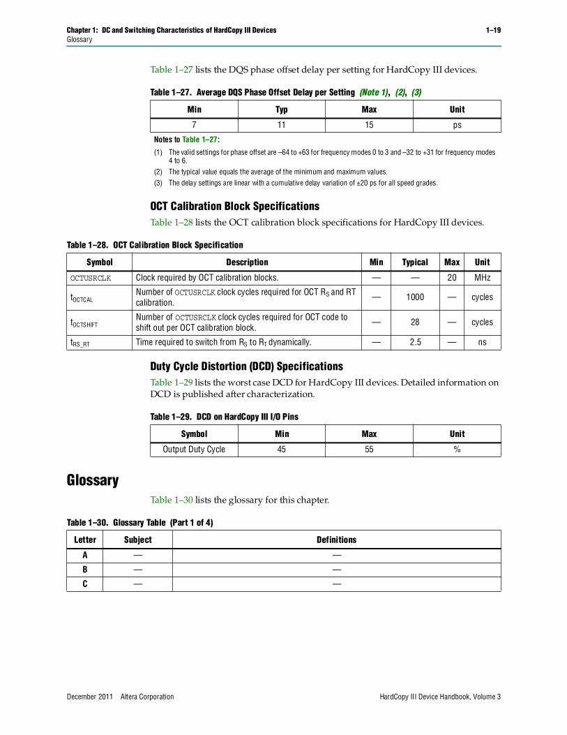
Chapter 1: DC and Switching Characteristics of HardCopy III Devices 1–19Glossary
December 2011 Altera Corporation HardCopy III Device Handbook, Volume 3
Table 1–27 lists the DQS phase offset delay per setting for HardCopy III devices.
OCT Calibration Block SpecificationsTable 1–28 lists the OCT calibration block specifications for HardCopy III devices.
Duty Cycle Distortion (DCD) SpecificationsTable 1–29 lists the worst case DCD for HardCopy III devices. Detailed information on DCD is published after characterization.
GlossaryTable 1–30 lists the glossary for this chapter.
Table 1–27. Average DQS Phase Offset Delay per Setting (Note 1), (2), (3)
Min Typ Max Unit
7 11 15 ps
Notes to Table 1–27:
(1) The valid settings for phase offset are –64 to +63 for frequency modes 0 to 3 and –32 to +31 for frequency modes 4 to 6.
(2) The typical value equals the average of the minimum and maximum values.(3) The delay settings are linear with a cumulative delay variation of ±20 ps for all speed grades.
Table 1–28. OCT Calibration Block Specification
Symbol Description Min Typical Max Unit
OCTUSRCLK Clock required by OCT calibration blocks. — — 20 MHz
tOCTCALNumber of OCTUSRCLK clock cycles required for OCT RS and RT calibration.
— 1000 — cycles
tOCTSHIFTNumber of OCTUSRCLK clock cycles required for OCT code to shift out per OCT calibration block.
— 28 — cycles
tRS_RT Time required to switch from RS to RT dynamically. — 2.5 — ns
Table 1–29. DCD on HardCopy III I/O Pins
Symbol Min Max Unit
Output Duty Cycle 45 55 %
Table 1–30. Glossary Table (Part 1 of 4)
Letter Subject Definitions
A — —
B — —
C — —

1–20 Chapter 1: DC and Switching Characteristics of HardCopy III DevicesGlossary
HardCopy III Device Handbook, Volume 3 December 2011 Altera Corporation
DDifferential I/O Standards
Figure 1–2. Receiver Input Waveforms
Transmitter Output Waveforms
E — —
F
fHSCLK High-speed I/O Block: High-speed receiver/transmitter input and output clock frequency.
fHSDR High-speed I/O Block: Maximum/minimum LVDS data transfer rate (fHSDR = 1/TUI), non-DPA.
fHSDRDPA High-speed I/O Block: Maximum/minimum LVDS data transfer rate (fHSDRDPA = 1/TUI), DPA.
G — —
H — —
I — —
J
J High-speed I/O Block: Deserialization factor (width of parallel data bus).
JTAG Timing Specifications
Figure 1–3. JTAG Timing Specifications
K — —
L — —
M — —
N — —
O — —
Table 1–30. Glossary Table (Part 2 of 4)
Letter Subject Definitions
Single-Ended Waveform
Differential Waveform
Positive Channel (p) = VIH
Negative Channel (n) = VIL
Ground
VID
VID
VID
p − n = 0 V
VCM
Single-Ended Waveform
Differential Waveform
Positive Channel (p) = VOH
Negative Channel (n) = VOL
Ground
VOD
VOD
VOD
p − n = 0 V
VCM
TDO
TCK
tJPZX tJPCO
tJPH
tJPXZ
tJCP
tJPSU tJCL tJCH
TDI
TMS

Chapter 1: DC and Switching Characteristics of HardCopy III Devices 1–21Glossary
December 2011 Altera Corporation HardCopy III Device Handbook, Volume 3
P PLL Specifications
The block diagram shown in the following figure highlights the PLL specification parameters:
Figure 1–4. Diagram of PLL Specifications (Note 1)
Note to Figure 1–4:
(1) Core clock can only be fed by dedicated clock input pins or PLL outputs.
Q — —
R RL Receiver differential input discrete resistor (external to HardCopy III device).
S
SW (sampling window)
The period of time during which the data must be valid to capture it correctly. The setup and hold times determine the ideal strobe position in the sampling window.
Figure 1–5. Timing Diagram
Single-ended Voltage Referenced I/O Standard
The JEDEC standard for SSTl and HSTL I/O standards defines both the AC and DC input signal values. The AC values indicate the voltage levels at which the receiver must meet its timing specifications. The DC values indicate the voltage levels at which the final logic state of the receiver is unambiguously defined. After the receiver input has crossed the AC value, the receiver changes to the new logic state.
The new logic state maintains as long as the input stays beyond the DC threshold. This approach provides predictable receiver timing in the presence of input waveform ringing.
Figure 1–6. Single-Ended Voltage Referenced I/O Standard
Table 1–30. Glossary Table (Part 3 of 4)
Letter Subject Definitions
Core Clock
External FeedbackReconfigurable in User Mode
Key
CLK
N
M
PFD
Switchover
VCOCP LF
CLKOUT Pins
GCLK
RCLK
fINPFDfIN
fVCO fOUT
fOUT_EXT
Counters
C0..C9
Bit Time
0.5 x TCCS RSKM Sampling Window (SW)
RSKM 0.5 x TCCS
VIH(AC)
VIH(DC)
VREFVIL(DC)
VIL(AC)
VOH
VOL
VCCIO
VSS

1–22 Chapter 1: DC and Switching Characteristics of HardCopy III DevicesGlossary
HardCopy III Device Handbook, Volume 3 December 2011 Altera Corporation
T
tC High-speed receiver and transmitter input and output clock period.
TCCS (channel-to-channel-skew)
The timing difference between the fastest and the slowest output edges, including tCO variation and clock skew, across channels driven by the same PLL. The clock is in the TCCS measurement (refer to Figure 1–5 under S in this table).
tDUTY
High-speed I/O Block: Duty cycle on high-speed transmitter output clock.
Timing Unit Interval (TUI)
The timing budget allowed for skew, propagation delays, and data sampling window. (TUI = 1/(Receiver Input Clock Frequency Multiplication Factor) = tC/w)
tFALL Signal high-to-low transition time (80-20%)
tINCCJ Cycle-to-cycle jitter tolerance on PLL clock input
tOUTPJ_IO Period jitter on general purpose I/O driven by a PLL
tOUTPJ_DC Period jitter on dedicated clock output driven by a PLL
tRISE Signal low-to-high transition time (20–80%)
U — —
V
VCM(DC) DC common mode input voltage.
VICM Input common mode voltage: The common mode of the differential signal at the receiver.
VIDInput differential voltage swing: The difference in voltage between the positive and complementary conductors of a differential transmission at the receiver.
VDIF(AC) AC differential input voltage: Minimum AC input differential voltage required for switching.
VDIF(DC) DC differential input voltage: Minimum DC input differential voltage required for switching.
VIHVoltage input high: The minimum positive voltage applied to the input that the device accepts as a logic high.
VIH(AC) High-level AC input voltage
VIH(DC) High-level DC input voltage
VILVoltage input low: The maximum positive voltage applied to the input that the device accepts as a logic low.
VIL(AC) Low-level AC input voltage
VIL(DC) Low-level DC input voltage
VOCMOutput common mode voltage: The common mode of the differential signal at the transmitter.
VODOutput differential voltage swing: The difference in voltage between the positive and complementary conductors of a differential transmission at the transmitter.
W W High-speed I/O Block: Clock boost factor
X — —
Y — —
Z — —
Table 1–30. Glossary Table (Part 4 of 4)
Letter Subject Definitions

Chapter 1: DC and Switching Characteristics of HardCopy III Devices 1–23Document Revision History
December 2011 Altera Corporation HardCopy III Device Handbook, Volume 3
Document Revision HistoryTable 1–31 lists the revision history for this document.
Table 1–31. Document Revision History
Date Version Changes
December 2011 4.1
■ Updated operating junction temperature value in Table 1–1.
■ Updated Device Recommended Operating Conditions
■ Added Table 1–6 Bus Hold Specifications
■ Updated Differential I/O Standard Specifications
■ Updated HardCopy III I/O pin leakage current value.
■ Updated supply current specifications for VCC_CLKIN and VCCPGM values.
■ Updated JTAG timing parameters values.
■ Updated DSP block performance specification.
■ Updated the TriMatrix memory block performance specifications.
■ Updated DLL frequency range specifications.
■ Updated hot socketing values.
■ Updated device capacitance values.
■ Updated internal weak pull-up resistor values.
■ Updated I/O OCT resistance tolerance values.
■ Updated OCT with calibration specification values.
■ Updated OCT variation after power-up calibration values.
■ Updated PLL specification values.
January 2011 4.0
■ Updated Table 1–19, Table 1–21, and Table 1–23.
■ Removed “External Memory Interface Specifications” and “I/O Timing” sections .
■ Added a note to Table 1–23.
■ Updated the “Glossary” section.
■ Made general editorial changes.
■ Updated to the new document template.
June 2009 3.0 Added new part numbers and clock tree performance specifications (Table 1–18).
December 2008 2.0
■ Updated Table 1–3.
■ Updated Table 1–19.
■ Updated Table 1–23.
■ Made minor editorial changes.
May 2008 1.0 Initial release.

1–24 Chapter 1: DC and Switching Characteristics of HardCopy III DevicesDocument Revision History
HardCopy III Device Handbook, Volume 3 December 2011 Altera Corporation

HardCopy III Device Handbook, Volume 3: DatasheetMarch 2012
HIII52002-1.0
Subscribe
© 2012 Altera Corporation. All rights reserved. ALTERA, ARRIA, CYCLONE, HARDCOPY, MAX, MEGACORE, NIOS, QUARTUS and STRATIX are Reg. U.S. Pat. & Tm. Off. and/or trademarks of Altera Corporation in the U.S. and other countries. All other trademarks and service marks are the property of their respective holders as described at www.altera.com/common/legal.html. Altera warrants performance of its semiconductor products to current specifications in accordance with Altera’s standard warranty, but reserves the right to make changes to any products and services at any time without notice. Altera assumes no responsibility or liability arising out of the application or use of any information, product, or service described herein except as expressly agreed to in writing by Altera. Altera customers are advised to obtain the latest version of device specifications before relying on any published information and before placing orders for products or services.
2. Extended Temperature Range forHardCopy III Devices
As part of the Altera® initiative to provide enhanced commercial off-the-shelf (COTS) devices for wider applications, the temperature range for the HardCopy® III device families has been extended to enable operation across the extended temperature range (–40°C to 125°C). This extension allows design engineers who are working on systems with stringent temperature requirements to benefit from the cost savings by using commercially available HardCopy III ASICs.
HardCopy III ASICs are extremely robust and capable of operating across a wide temperature range with excellent reliability. This chapter describes the Altera support for HardCopy III extended temperature range operation with the appropriate background information. It also explains how to use HardCopy III devices across the extended temperature range operation, along with any limitations in operation that affect the HardCopy III datasheet specifications.
These guidelines have been determined through additional characterization of HardCopy III devices on samples of production silicon across the extended temperature ranges (125°C and –40°C). While characterizations demonstrate correct operation across extended temperatures by design, production testing of industrial grade devices for extended temperature range operation is performed at 100°C.
Extended Temperature SupportExtended temperature operation requires additional timing margin over industrial temperature operation to compensate for the potentially increased variation of fMAX across temperature. For the Stratix® III FPGA prototype devices, the increased timing margin is achieved by compiling the design using an industrial I4 part and setting the temperature range from –40°C to 125°C in the Quartus® II software. The Quartus II software provides separate timing models at 125°C for slow corner and –40°C for fast corner. By selecting a HardCopy III companion device and extended temperature range (–40°C min and 125°C max) in the operating temperature condition, the Quartus II software uses the appropriate timing models to ensure that the constraints of extended temperature range operation are met.
The extended temperature range support design flow is the same as that for commercial and industrial devices. Use the Quartus II HardCopy III Advisor to help guide you through the flow to ensure your design is ready for submission to the Altera HardCopy Design Center.
Table 2–1 lists the HardCopy III device part numbers that support the extended temperature operation.
Table 2–1. HardCopy III Extended Temperature Support
HardCopy Family Device Package Extended Temperature Support
HardCopy IIIHC325 All Yes
HC335 All Yes
March 2012HIII52002-1.0

2–2 Chapter 2: Extended Temperature Range for HardCopy III DevicesLimitations to Datasheet Specifications
HardCopy III Device Handbook, Volume 3: Datasheet March 2012 Altera Corporation
Software SupportThe HardCopy III extended temperature grade device models are supported in the following versions of these tools:
■ The PowerPlay Early Power Estimator (EPE) or the PowerPlay Power Analyzer software, version 11.1 or later. Download these tools from: www.altera.com/support/devices/estimator/pow-powerplay.html
■ The Quartus II software, version 11.1 or later. Download the software from:www.altera.com/products/software/quartus-ii/subscription-edition/qts-se-index.html
Limitations to Datasheet SpecificationsThis section describes the limitations to the HardCopy III datasheet specifications when operating HardCopy III devices at extended temperature range. Characterization results show that HardCopy III device operation across the extended temperature range is bounded by the industrial grade of the datasheet specifications and any relevant errata, except where noted below.
DSP Block SpecificationsTable 2–2 lists the HardCopy III DSP block performance specifications.
Table 2–2. HardCopy III DSP Block Performance Specifications (Note 1)
Mode Number of Multipliers
Maximum FrequencyUnit
Flipchip Wirebond
9 x 9-bit multiplier (a, c, e, g) (2) 1 315 252 MHz
9 x 9-bit multiplier (b, d, f, h) (2) 1 375 300 MHz
12 x 12-bit multiplier (a, e) (3) 1 315 252 MHz
12 x 12-bit multiplier (b, d, f, h) (3) 1 375 300 MHz
18 x 18-bit multiplier 1 400 320 MHz
36 x 36-bit multiplier 1 315 252 MHz
Double mode 1 315 252 MHz
18 x 18-bit multiply accumulator 4 330 264 MHz
18 x 18-bit multiply adder 4 345 276 MHz
18 x 18-bit multiply adder-signed full precision 2 345 276 MHz
18 x 18-bit multiply adder with loopback (4) 2 300 240 MHz
36-bit shift (32-bit data) 1 330 264 MHz
Notes to Table 2–2:
(1) The maximum is for a fully pipelined block with round and saturation disabled.(2) The DSP block implements eight independent 9 x 9-bit multipliers using a, b, c, and d for the top half of the DSP block;
and e, f, g, and h for the bottom half of the DSP block multipliers.(3) The DSP block implements six independent 12 x 12-bit multipliers using a, b, and d for the top half of the DSP block;
and e, f, and h for the bottom half of the DSP block multipliers.(4) The maximum for a non-pipelined block with loopback input registers disabled with round and saturation disabled.

Chapter 2: Extended Temperature Range for HardCopy III Devices 2–3Limitations to Datasheet Specifications
March 2012 Altera Corporation HardCopy III Device Handbook, Volume 3: Datasheet
TriMatrix Memory Block SpecificationsTable 2–3 lists the HardCopy III TriMatrix memory block specifications.
Table 2–3. HardCopy III TriMatrix Memory Block Performance Specifications (Part 1 of 2)
Memory Mode TriMatrix Memory
Maximum FrequencyUnit
Flipchip Wirebond
MLAB
Single port 16 × 10 1 450 338 MHz
Simple dual-port 16 × 20 1 450 338 MHz
ROM 64 × 10 1 450 338 MHz
ROM 32 × 20 1 450 338 MHz
M9K
Single-port 8K × 1 1 405 304 MHz
Single-port 4K × 2 or 2K × 4 1 405 304 MHz
Single-port 1K × 9, 512 × 18, or 256 × 36 1 460 345 MHz
Simple dual-port, 8K × 1 1 400 300 MHz
Simple dual-port, 4K × 2 or 2K × 4 1 400 300 MHz
Simple dual-port, 1K × 9, 512 × 18, or 256 × 36
1 400 300 MHz
Simple dual-port, 8K × 1, 4K × 2, or 2K × 4 with the read-during-write option set to “Old Data”
1 265 199 MHz
Simple dual-port, 1K × 9, 512 × 18, or 256 × 36 with the read-during-write option set to “Old Data”
1 265 199 MHz
True dual-port, 8K × 1 1 435 326 MHz
M9K
True dual-port, 4K × 2 or 2K × 4 1 370 278 MHz
True dual-port, 1K × 9 or 512 × 18 1 370 278 MHz
True dual-port, 8K × 1, 4K × 2, or 2K × 4 with the read-during-write option set to “Old Data”
1 245 184 MHz
True dual-port, 1K × 9 or 512 × 18 with the read-during-write option set to “Old Data”
1 245 184 MHz
ROM 1P, 8K × 1, 4K × 2, or 2K × 4 1 405 304 MHz
ROM 1P, 1K × 9, 512 × 18, or 256 × 36 1 405 304 MHz
ROM 2P, 8K × 1, 4K × 2, or 2K × 4 1 405 304 MHz
ROM 2P, 1K × 9, or 512 × 18 1 405 304 MHz
Min Pulse Width (Clock High Time) — 800 1067 ps
Min Pulse Width (Clock Low Time) — 625 831 ps

2–4 Chapter 2: Extended Temperature Range for HardCopy III DevicesDocument Revision History
HardCopy III Device Handbook, Volume 3: Datasheet March 2012 Altera Corporation
Transceiver Performance SpecificationsTransceiver performance is supported up to 3Gbps protocols only.
f For additional information about extended temperature support, refer to the Stratix III Military Temperature Range Support Technical Brief.
Document Revision HistoryTable 2–4 lists the revision history for this document.
M144K
True dual-port 16K × 9 or 8K × 18 1 310 233 MHz
True dual-port 4K × 36 1 310 233 MHz
Simple dual-port 16K × 9 or 8K × 18 1 325 244 MHz
Simple dual-port 4K × 36 or 2K × 72 1 325 244 MHz
ROM 1 Port 1 420 315 MHz
ROM 2 Port 1 380 285 MHz
Single-port 16K × 9 or 8K × 18 1 350 263 MHz
Single-port 4K × 36 1 350 263 MHz
True dual-port 16K × 9, 8K × 18, or 4K × 36 with the read-during-write option set to “Old Data”
1 200 150 MHz
M144K
Simple dual-port 16K × 9, 8K × 18, 4K × 36, or 2K × 72 with the read-during-write option set to “Old Data”
1 200 150 MHz
Simple dual-port 2K × 64 (with ECC) 1 245 171 MHz
Min Pulse Width (Clock High Time) — 1382 1843 ps
Min Pulse Width (Clock Low Time) — 690 920 ps
Table 2–3. HardCopy III TriMatrix Memory Block Performance Specifications (Part 2 of 2)
Memory Mode TriMatrix Memory
Maximum FrequencyUnit
Flipchip Wirebond
Table 2–4. Document Revision History
Date Version Changes
March 2012 1.0 Initial release.

March 2012 Altera Corporation HardCopy III Device Handbook, Volume 3: Datasheet
Additional Information
This chapter provides additional information about the document and Altera.
How to Contact AlteraTo locate the most up-to-date information about Altera products, refer to the following table.
Typographic ConventionsThe following table shows the typographic conventions this document uses.
Contact (1) Contact Method Address
Technical support Website www.altera.com/support
Technical trainingWebsite www.altera.com/training
Email [email protected]
Product literature Website www.altera.com/literature
Non-technical support (General) Email [email protected]
(Software Licensing) Email [email protected]
Note to Table:
(1) You can also contact your local Altera sales office or sales representative.
Visual Cue Meaning
Bold Type with Initial Capital Letters
Indicate command names, dialog box titles, dialog box options, and other GUI labels. For example, Save As dialog box. For GUI elements, capitalization matches the GUI.
bold typeIndicates directory names, project names, disk drive names, file names, file name extensions, software utility names, and GUI labels. For example, \qdesigns directory, D: drive, and chiptrip.gdf file.
Italic Type with Initial Capital Letters Indicate document titles. For example, Stratix IV Design Guidelines.
italic typeIndicates variables. For example, n + 1.
Variable names are enclosed in angle brackets (< >). For example, <file name> and <project name>.pof file.
Initial Capital Letters Indicate keyboard keys and menu names. For example, the Delete key and the Options menu.
“Subheading Title” Quotation marks indicate references to sections within a document and titles of Quartus II Help topics. For example, “Typographic Conventions.”

Info–2 Additional InformationTypographic Conventions
HardCopy III Device Handbook, Volume 3: Datasheet March 2012 Altera Corporation
Courier type
Indicates signal, port, register, bit, block, and primitive names. For example, data1, tdi, and input. The suffix n denotes an active-low signal. For example, resetn.
Indicates command line commands and anything that must be typed exactly as it appears. For example, c:\qdesigns\tutorial\chiptrip.gdf.
Also indicates sections of an actual file, such as a Report File, references to parts of files (for example, the AHDL keyword SUBDESIGN), and logic function names (for example, TRI).
r An angled arrow instructs you to press the Enter key.
1., 2., 3., anda., b., c., and so on
Numbered steps indicate a list of items when the sequence of the items is important, such as the steps listed in a procedure.
■ ■ ■ Bullets indicate a list of items when the sequence of the items is not important.
1 The hand points to information that requires special attention.
h A question mark directs you to a software help system with related information.
f The feet direct you to another document or website with related information.
c A caution calls attention to a condition or possible situation that can damage or destroy the product or your work.
w A warning calls attention to a condition or possible situation that can cause you injury.
The envelope links to the Email Subscription Management Center page of the Altera website, where you can sign up to receive update notifications for Altera documents.
Visual Cue Meaning