gm 47/gm 48 - electronic component · pdf fileat commands. it is assumed that ... sony...
TRANSCRIPT

GM 47/GM 48Technical Description

CEThe product described in this manual conforms to the Radio Equipment and Telecommunication TerminalEquipment (R&TTE) directive 99/5/EC with requirements covering EMC directive 89/336/EEC andLow Voltage directive 73/23/EEC. The product fulfils the requirements according to 3GPP TS 51.010-1,EN 301489-7 and EN60950.
The information contained in this document is the proprietary information of Sony Ericsson MobileCommunications. The contents are confidential and any disclosure to persons other than the officers,employees, agents or subcontractors of the owner or licensee of this document, without the prior writtenconsent of Sony Ericsson Mobile Communications, is strictly prohibited.
Further, no portion of this publication may be reproduced, stored in a retrieval system, or transmitted inany form or by any means, electronic or mechanical, including photocopying and recording, without theprior written consent of Sony Ericsson Mobile Communications, the copyright holder.
Third edition (June 2002)
Sony Ericsson Mobile Communications. publishes this manual without making any warranty as to thecontent contained herein. Further Sony Ericsson Mobile Communications. reserves the right to makemodifications, additions and deletions to this manual due to typographical errors, inaccurate information,or improvements to programs and/or equipment at any time and without notice. Such changes will,nevertheless be incorporated into new editions of this manual.
All rights reserved.
© Sony Ericsson Mobile Communications., 2002
Publication number:
Printed in UK

GM47/GM48 Technical description
BA/SEM/MS 02:0004 Rev C 3
Contents1 INTRODUCTION....................................................................................................................5
1.1 OVERVIEW ........................................................................................................................51.2 FEATURES.........................................................................................................................6
1.2.1 Type of Mobile Station .............................................................................................61.2.2 SMS .........................................................................................................................71.2.3 Voice calls ................................................................................................................71.2.4 Data..........................................................................................................................71.2.5 SIM Card ..................................................................................................................81.2.6 Power consumption..................................................................................................81.2.7 Other features ..........................................................................................................81.2.8 Development Kit.......................................................................................................8
1.3 PRECAUTIONS ...................................................................................................................81.4 ABBREVIATIONS.................................................................................................................9
2 MECHANICAL DESCRIPTION............................................................................................102.1 INTERFACE DESCRIPTION.................................................................................................102.2 PHYSICAL DIMENSIONS ....................................................................................................11
3 SYSTEM CONNECTOR INTERFACE.................................................................................123.1 OVERVIEW ......................................................................................................................123.2 GENERAL ELECTRICAL AND LOGICAL CHARACTERISTICS....................................................15
3.2.1 General Protection Requirements..........................................................................153.3 GROUNDS .......................................................................................................................16
3.3.1 The Analogue Ground............................................................................................163.3.2 The Digital Ground (DGND)...................................................................................16
3.4 REGULATED POWER SUPPLY ...........................................................................................173.4.1 Power Supply (VCC)..............................................................................................17
3.5 ON/OFF AND EXTERNAL POWER SIGNALS .......................................................................173.5.1 Module ON/OFF.....................................................................................................173.5.2 External 2.75 V (VIO) .............................................................................................18
3.6 ANALOGUE AUDIO ...........................................................................................................193.6.1 Audio To Mobile Station (ATMS) ...........................................................................193.6.2 Audio From Mobile Station (AFMS) .......................................................................21
3.7 MICROPHONE SIGNALS ....................................................................................................213.8 SPEAKER SIGNALS ..........................................................................................................223.9 DIGITAL AUDIO ................................................................................................................223.10 SERIAL DATA...................................................................................................................24
3.10.1 UART 1 (RS232) - RD, TD, RTS, CTS, DTR, DCD and RI ...................................253.10.2 Serial Data Signals - RD, TD .................................................................................253.10.3 Control Signals - RTS, CTS, DTR, DCD, RI ..........................................................263.10.4 UART 2 - TD2, RD2 ...............................................................................................283.10.5 UART 3 - TD3, RD3 ...............................................................................................28
3.11 SIM CARD RELATED SIGNALS...........................................................................................293.11.1 SIM Detection – SIM Presence..............................................................................30
3.12 SERVICE/PROGRAMMING .................................................................................................303.13 BUZZER ..........................................................................................................................313.14 LED................................................................................................................................313.15 TX_ON - BURST TRANSMISSION......................................................................................323.16 TIMESTAMP .....................................................................................................................323.17 REAL TIME CLOCK...........................................................................................................33
4 ANTENNA CONNECTOR....................................................................................................34

GM47/GM48 Technical description
BA/SEM/MS 02:0004 Rev C 4
5 AT COMMAND SUMMARY.................................................................................................35
6 TECHNICAL DATA..............................................................................................................38
7 CONTACT DETAILS............................................................................................................40
GM47/GM48 Technical description
BA/SEM/MS 02:0004 Rev C 5
1 Introduction
1.1 OverviewThe GM47/GM48 belong to a new generation of Sony EricssonMobile Communications GSM modules. This document describes themain characteristics and functionality of the GM 47/48, two dual bandproducts for 900/1800 MHz and 850/1900 MHz GSM bandsrespectively.
They are intended to be used in both machine-to-machine applicationsand man-to-machine applications. The module serves its purposewhen there is a need for sending and receiving data (by SMS, CSD,HSCSD, or GPRS), as well as making voice calls over the GSMnetwork.
GM47/GM48 are business-to-business products. It is intended to besold to manufacturers, system integrators, applications developers-developing solutions with wireless communication. The module isintended to be integrated by the system integrator within anapplication. The module and the external application will form asystem for wireless communication.
A typical system is one where a micro controller in an externalapplication communicates with the module over its serial interface.The micro controller will control the module, via the supported set ofAT commands. It is assumed that the system integrators have a hightechnical knowledge and the ability to integrate the module into asystem. For the GM47/GM48 modules some interesting applicationsare the following:
• Fleet and Asset Management
• Vending Machines
• Security and Alarm
• Other telemetry applications

GM47/GM48 Technical description
BA/SEM/MS 02:0004 Rev C 6
1.2 FeaturesThe module performs a set of telecom services (TS) according toGSM standard phase 2+, ETSI and ITU-T. The functions of themodule are implemented by issuing AT commands over the serialinterface. Supported AT commands are listed in section 5, these aredefined further in GSM 7.05/7.07 and the GM47/GM48 integratorsmanual.
1.2.1 Type of Mobile StationThe GM 4X family are normal dual band type of MS with thefollowing characteristics.
GM 47 GSM 900 E-GSM 900 GSM 1800
Frequency Range(MHz)
TX: 890-915
RX: 935-960
TX: 880-890
RX: 925-935
TX: 1710-1785
RX: 1805-1880
Channel spacing 200 kHz 200 kHz
Number of channels 173 Carriers *8 (TDMA)
GSM: Channels 1 to 124
E-GSM: Channels 975 to 1023
374 Carriers *8 (TDMA)
DCS: Channels 512 to 885
Modulation GMSK GMSK
TX Phase Accuracy < 5º RMS Phase error (burst) < 5º RMS Phase error (burst)
Duplex spacing 45 MHz 95 MHz
Receiver sensitivity atantenna connector
< - 102 dBm < - 102 dBm
Transmitter outputpower at antennaconnector
Class 4
2W (33 dBm)
Class 1
1W (30 dBm)
Automatic hand-over between GSM 900 and GSM 1800
GM 48 GSM 850 GSM 1900
Frequency Range (MHz) TX: 824-849
RX: 869-894
TX: 1850-1910
RX: 1930-1990
Channel spacing 200 kHz 200 kHz
Number of channels 123 carriers *8 (TDMA)
GSM: Channels 128 to 251
298 Carriers *8 (TDMA)
PCS: Channels 512 to 810
Modulation GMSK GMSK
TX Phase Accuracy < 5º RMS Phase error (burst) < 5º RMS Phase error (burst)
Duplex spacing 45 MHz 80 MHz
Receiver sensitivity at antennaconnector
< - 102 dBm < - 102 dBm
Transmitter output power atantenna connector
Class 5
0.8 W (29 dBm)
Class 1
1W (30 dBm)
Automatic hand-over between GSM 850 and GSM 1900
GM47/GM48 Technical description
BA/SEM/MS 02:0004 Rev C 7
1.2.2 SMSThe module supports the following SMS services:
• Sending: MO, both PDU and Text mode supported.• Receiving: MT, both PDU and Text mode supported.• CBM is a service, in which a message is sent to all subscribers
located in one or more specific cell(s) in the GSM network, forexample, cell location information.
• SMS STATUS REPORT according to GSM 03.40.
The maximum length of an SMS message is 160 characters whenusing 7-bit encoding. For 8-bit data, the maximum length is 140characters.
The module supports upto 6 concatenated messages to extend thisfunction.
1.2.3 Voice callsThe GM47/GM48 offers the capability of MO and MT voice calls, aswell as supporting emergency calls. In addition to this multiparty, callwaiting and call deflection features are available. Some of thesefeatures are operator specific.
The module offers normal analogue input/output lines, analogue audioinput/ output lines in differential modes, and digital audio interface,with the possibility of accessing internal points within the digitalaudio lines. Moreover, the GM47/GM48 have embedded echocanceller and noise suppresser, which provide high quality audio.
The module supports HR, FR and EFR voice coding, provided thatEFR is available in the network.
1.2.4 DataThe module supports the following data protocols:
• General Packet Radio Service (GPRS). The modules are Class BTerminals, which provides simultaneous activation and attach ofGPRS and GSM services. The GM47/GM48 modules are GPRS4+1 devices, which are capable of transmitting in one timeslot perframe (uplink), and receiving in a maximum of four timeslots perframe (downlink).
• Circuit Switched Data (CSD). GM47/GM48 modules are capableof establishing a circuit switch data link at 9.6 kbps.
• High Speed Circuit Switched Data (HSCSD).GM47/GM48supports HSCSD communication, with one timeslotper frame capacity in the uplink and two timeslots per framecapacity in the downlink (2+1).

GM47/GM48 Technical description
BA/SEM/MS 02:0004 Rev C 8
1.2.5 SIM Card
The module supports the connection of an external SIM Card with 3Vor 5 V technology, via the 60-pin system connector. The module doesnot have an internal SIM holder.
1.2.6 Power consumption
Stand-by Transmit/Operation
GSM 850 & 900 MHz <5 mA 275 mA (2A peak)
GSM 1800 & 1900 MHz <5 mA 250 mA (1.75A peak)
Note! The power consumption during transmission is measured atmaximum transmit power.
1.2.7 Other features
• 07.10 Multiplexing
• GPS interoperability
• SIM application toolkit, class 2 release 96 compliant
1.2.8 Development Kit
Sony Ericsson Mobile Communications provides the opportunity totest the module in a limited scale, before ordering a large quantity.With the development kit you can quickly get started with the module.The kit includes necessary accessories (software and hardware) thatyou will need for your test purposes. It also includes the following:
• GSM module GM 47 or GM 48
• Integrator’s Manual
The Integrator’s Manual provides you with all the information youneed to be able to integrate the module with your application.
This is available from your regional salesperson or M2M customersupport (see section 7)
1.3 PrecautionsThe GM47/GM48should be handled like any mobile station. In theIntegrators’ Manual you will find more information about safety andproduct care. In the Technical Data chapter in this document the
GM47/GM48 Technical description
BA/SEM/MS 02:0004 Rev C 9
environmental and electrical limits are specified. Never exceed theselimits to ensure the module is not damaged.
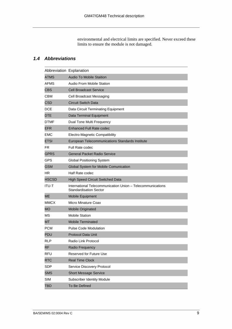
1.4 Abbreviations
Abbreviation ExplanationATMS Audio To Mobile Staition
AFMS Audio From Mobile Station
CBS Cell Broadcast Service
CBM Cell Broadcast Messaging
CSD Circuit Switch Data
DCE Data Circuit Terminating Equipment
DTE Data Terminal Equipment
DTMF Dual Tone Multi Frequency
EFR Enhanced Full Rate codec
EMC Electro-Magnetic Compatibility
ETSI European Telecommunications Standards Institute
FR Full Rate codec
GPRS General Packet Radio Service
GPS Global Positioning System
GSM Global System for Mobile Comunication
HR Half Rate codec
HSCSD High Speed Circuit Switched Data
ITU-T International Telecommunication Union – TelecommunicationsStandardisation Sector
ME Mobile Equipment
MMCX Micro Minature Coax
MO Mobile Originated
MS Mobile Station
MT Mobile Terminated
PCM Pulse Code Modulation
PDU Protocol Data Unit
RLP Radio Link Protocol
RF Radio Frequency
RFU Reserved for Future Use
RTC Real Time Clock
SDP Service Discovery Protocol
SMS Short Message Service
SIM Subscriber Identity Module
TBD To Be Defined

GM47/GM48 Technical description
BA/SEM/MS 02:0004 Rev C 10
2 Mechanical Description
2.1 Interface Description
The picture below presents the conceptual mechanical design of theGM 47/48. The GM 47/48 are protected with AISI 304 Stainless Steelcovers suitable to fulfil the environmental and EMC requirements.Dimensions, the position of the different connectors and mountingholes are shown in figure 2.2.
Figure 2.1 GM 47/48, view from the underside

GM47/GM48 Technical description
BA/SEM/MS 02:0004 Rev C 11
2.2 Physical Dimensions
Figure 2.2 Physical dimensions of GM 47/48
The measures are given in millimetre’s. See also chapter 6, TechnicalData.

GM47/GM48 Technical description
BA/SEM/MS 02:0004 Rev C 12
3 System Connector Interface
3.1 Overview
The electrical connections to the module (except the antenna), aremade through the System Connector Interface.
The connector shall allow the following connections: board to boardand board to cable. Details of connector availability and sources areavailable from customer support on request.
Figure 3.1 GM 47/48. View from the underside
The table on next page provides the pin assignment of the differentsignals in the System Connector Interface as well as a shortdescription of them.
All signal directions are with respect to the module i.e. Direction 'O'means data being sent by the module.
GM47/GM48 Technical description
BA/SEM/MS 02:0004 Rev C 13
Pin Signal Name Dir Signal Type Description
1. VCC I Supply Power Supply
2. DGND - - Digital Ground
3. VCC I Supply Power Supply
4. DGND - - Digital Ground
5. VCC I Supply Power Supply
6. DGND - - Digital Ground
7. VCC I Supply Power Supply
8. DGND - - Digital Ground
9. VCC I Supply Power Supply
10. DGND - - Digital Ground
11. VCC I Supply Power Supply
12. DGND - - Digital Ground
13. Reserved for future use
14. ON/OFF I Internal pull up,open drain
Turns the module on/off
Former WAKE_B
15. SIMVCC - Dig. 3/5 V SIM card power supply
Power output for SIM Card from module
16. SIMPRESENCE I Internal pull up,open drain
SIM Presence
A "1" shall indicate that the SIM is missing;a "0" that it is inserted.
17. SIMRST O Dig. 3/5 V SIM card reset
18. SIMDATA I/O Dig. 3/5 V SIM card data
19. SIMCLK O Dig. 3/5 V SIM card clock
20. DAC O Analogue Digital to Analogue converter
21. IO1 I/O Digital, 2.75 General purpose input/output 1
22. IO2 I/O Digital, 2.75 General purpose input/output 2
23. IO3 I/O Digital, 2.75 General purpose input/output 3
24. IO4 I/O Digital, 2.75 General purpose input/output 4
25. VRTC I Supply 1.8 V Voltage for real time clock
26. ADC1 I Analogue Analogue to Digital converter 1
27. ADC2 I Analogue Analogue to Digital converter 2
28. ADC3 I Analogue Analogue to Digital converter 3
29. SDA I/O 2.75, internalpullup
I2C Data
30. SCL O 2.75, internalpullup
I2C Clock
31. BUZZER O Dig. 2.75 Buzzer output from module
32. TIMESTAMP O Dig. 2.75 Timestamp
Timestamp is reserved for future use,when A-GPS is implemented in the

GM47/GM48 Technical description
BA/SEM/MS 02:0004 Rev C 14
networks side.
33. LED O Dig. 2.75 Flashing LED
34. VIO O Power Out 2.75 Module powered indication.
The VIO is a 2.75 V output that couldpower external devices to transmit datatowards the GSM device to a 75mA max.
35. TX_ON O Dig 2.75 This output shall indicate when the GSMmodule is going to transmit the burst.
36. RI O Dig. 2.75 Ring Indicator
37. DTR I Dig. 2.75 Data Terminal Ready
38. DCD O Dig. 2.75 Data Carrier Detect
39. RTS I Dig. 2.75 Request To Send
40. CTS O Dig. 2.75 Clear To Send
41. TD I Dig. 2.75 Transmitted Data
Data from DTE (host) to DCE (module).[former DTMS]
42. RD O Dig. 2.75 Received Data
Data from DCE (module) to DTE (host).[former DFMS]
43. TD3 I Dig. 2.75 UART3 Transmission
Data from DTE (host) to DCE (module).[former DTMS]
44. RD3 O Dig. 2.75 UART3 Reception
Data from DCE (module) to DTE (host).[former DFMS]
45. TD2 I Dig. 2.75 UART2 Reception
Data from DTE (host) to DCE (module).
Former CTMS. Used for flashing
46. RD2 O Dig. 2.75 UART2 Transmission
Data from DCE (module) to DTE (host).
Former CFMS. Used for flashing
47. PCMULD I Dig. 2.75 DSP PCM digital audio input
48. PCMDLD O Dig. 2.75 DSP PCM digital audio output
49. PCMO O Dig. 2.75 Codec PCM digital audio output
50. PCMI I Dig. 2.75 Codec PCM digital audio input
51. PCMSYNC O Dig. 2.75 DSP PCM frame sync
52. PCMCLK O Dig. 2.75 DSP PCM clock output
53. MICP I Analogue Microphone input positive
54. MICN I Analogue Microphone input negative
55. BEARP O Analogue Speaker output positive
56. BEARN O Analogue Speaker output negative
57. AFMS O Analogue Audio output from module
58. SERVICE I 12V/2.7V Flash programming voltage for the MS.

GM47/GM48 Technical description
BA/SEM/MS 02:0004 Rev C 15
Enable logger information if no flashing
Former VPPFLASH
59. ATMS I Analogue Audio input to module
60. AGND - Analogue Analogue ground
3.2 General Electrical and Logical Characteristics
Many of the signals present in the interface are high-speed CMOSlogic inputs or outputs powered from 2.75 V ± 5 %. Whenever asignal is defined as Dig. 2.75 V, the following electricalcharacteristics shall apply.
Parameter Min. Typ. Max. Units Output
Current Io
High Level Output Voltage (VOH) 2.2 2.75 Volts - 2 mA
Low Level Output Voltage (VOL) 0 0.6 Volts 2 mA
High Level Input Voltage (VIH) 1.93 2.75 Volts
Low Level Input voltage (VIL) 0 0.5 Volts
3.2.1 General Protection Requirements
All 2.75V digital inputs shall continuously withstand any voltage from-0.5V up to 3.47V (3.3V + 5%) in the power-on or power-offcondition with no damage. All 2.75V digital outputs shallcontinuously withstand a short circuit to any voltage within the rangefrom 0V to 3V.
! Note : This is for protection ONLY, the module cannot be drivendirectly by a 3.3V micro processor, if this is done it will invalidate anywarranty claim on the module.
The SIM output signals and the SIMVCC supply can continuouslywithstand a short circuit to any voltage within the range from 0V to4.1V.
GM47/GM48 Technical description
BA/SEM/MS 02:0004 Rev C 16
3.3 Grounds
Pins Name Description
2, 4, 6, 8, 10, 12 DGND Digital Ground
60 AGND Analogue Ground
There are two ground signals in GM 47/48, Analogue Ground(AGND) and Digital Ground (DGND). The analogue Ground isconnected to pin number 60, and the Digital Ground is connected tothe System Connector Interface through pin numbers 2, 4, 6, 8, 10 and12.
Note: All the Ground pins have to be connected to the application.The AGND is connected to the DGND in the ME, and only there. It isimportant that the AGND and the DGND are separated in theapplication.
3.3.1 The Analogue Ground
The AGND lead is the analogue audio reference ground. It is thereturn signal for Audio To Mobile Station (ATMS) and Audio FromMobile Station (AFMS).
It shall be connected to the Digital Ground (DGND) inside the moduleand only there. The application shall not connect DGND and AGND.
Parameter Limit
Imax ≅ 12.5mA
3.3.2 The Digital Ground (DGND)
DGND is the reference for all digital signals in the System Interface.It shall also be the DC return for the power supply on VCC andSERVICE. Each DGND pin is rated at 0.5 A. All DGND pins areconnected internally in the module.
All DGND pins should be connected commonly in the application.
Parameter Limit
Iaverage < 0.5 A No DGND pin can withstand over 0.5 A
Imax < 600 mA (100 mA each)

GM47/GM48 Technical description
BA/SEM/MS 02:0004 Rev C 17
3.4 Regulated Power Supply
Pins Name Description
1, 3, 5, 7, 9, 11 VCC Regulated Power Supply
The regulated power supply, VCC, is connected to the pin numbers 1,3, 5, 7, 9 and 11.
3.4.1 Power Supply (VCC)
The VCC supplies the module with external power. Any other voltageneeded is generated internally.
Parameter Mode Limit
Voltage to be applied Nominal 3.6 Volts
Tolerance including ripple 1 3.4 Volts - 4.0 Volts
Over voltages 5.5 Volts
Current Drive capability at TX Full Power < 600 mA (average))
< 2 A (Peak)
GM 47/48 have not internal capacitance to supply the large currentpeaks during GSM transmission. Therefore on burst transmission theapplication DC source is responsible for providing the appropriatecurrent.
Design application notes are available from customer support onrequest.
3.5 ON/OFF and External Power Signals
Pins Name Dir Description
14 ON/OFF I Square signal to turn on/off the module
34 VIO O External power supply
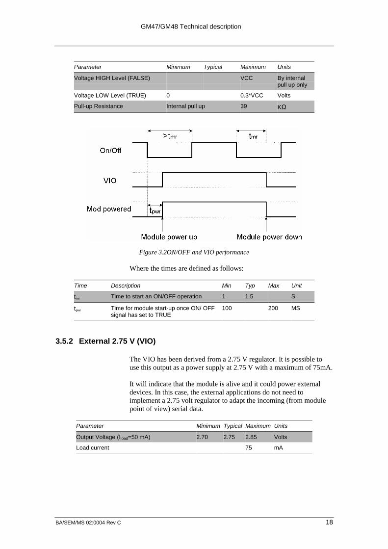
3.5.1 Module ON/OFF
The module is powered ON/OFF by grounding (pulling low) pin 14 asper figure 3.2 below. The pin should then be released as it has aninternal pull up to return it to the high state.
Note: Driving with 2.75V or 3.6V is not permitted and restrictsmodule functionality.
1 Measured at system connector pins.
GM47/GM48 Technical description
BA/SEM/MS 02:0004 Rev C 18
Parameter Minimum Typical Maximum Units
Voltage HIGH Level (FALSE) VCC By internalpull up only
Voltage LOW Level (TRUE) 0 0.3*VCC Volts
Pull-up Resistance Internal pull up 39 KΩ
Figure 3.2ON/OFF and VIO performance
Where the times are defined as follows:
Time Description Min Typ Max Unit
tmr Time to start an ON/OFF operation 1 1.5 S
tpwr Time for module start-up once ON/ OFFsignal has set to TRUE
100 200 MS
3.5.2 External 2.75 V (VIO)
The VIO has been derived from a 2.75 V regulator. It is possible touse this output as a power supply at 2.75 V with a maximum of 75mA.
It will indicate that the module is alive and it could power externaldevices. In this case, the external applications do not need toimplement a 2.75 volt regulator to adapt the incoming (from modulepoint of view) serial data.
Parameter Minimum Typical Maximum Units
Output Voltage (Iload=50 mA) 2.70 2.75 2.85 Volts
Load current 75 mA
GM47/GM48 Technical description
BA/SEM/MS 02:0004 Rev C 19
3.6 Analogue Audio
Pins Name Dir Description
57 AFMS O Audio From Mobile Station
59 ATMS I Audio To Mobile Station
60 AGND - Reference for analogue audio
ATMS and AFMS are the audio input and output for the module. Theanalogue audio signals can be used in two different modes, Handsfreeand Portable Handsfree.
HandsfreeThis mode is referred to as Audio To Mobile Station (ATMS) andAudio From Mobile Station (AFMS). It is used by audio accessoriessuch as Handsets and Handsfree equipment.
Portable HandsfreeThis mode activates a different amplification factor in the MobileEquipment (ME). It also activates a microphone bias level in ATMS.This is the default mode.
3.6.1 Audio To Mobile Station (ATMS)
ATMS is the analogue audio input to the module. It connects to theaudio input of the CODEC in the module. The CODEC then convertsthe analogue audio to digital audio, in PCM format, which isconnected to the internal PCM bus in the module. The internal PCMbus connects the encoded audio to PCMO on the system connector.
ATMS is also used as the microphone input from the PortableHandsfree. If this is the case, a DC bias is provided from the ATMS.
All sources must be AC-coupled except the Portable Handsfreemicrophone, which shall be DC-coupled in order to supply DC currentto the Portable Handsfree microphone. AC coupling prevents incorrectbiasing or damage of the ATMS input. The capacitor must have avalue greater than shown below to avoid attenuation of lowfrequencies.
The ATMS input is a passive network followed by the transmit part ofthe CODEC.

GM47/GM48 Technical description
BA/SEM/MS 02:0004 Rev C 20
Parameter Limit
Application driving impedance (0.3 - 3.5 kHz) < 300 Ω
AC coupling capacitance 2 > 1 µF
Module input impedance (0.3 - 3.5 kHz) >50ΚΩ
Low frequency cut-off (- 3 dB) 300 Hz ± 50 Hz
High frequency cut-off (- 3 dB) > 3500 Hz
Maximum allowed input level 1.5Vpp = 530mV
Output DC bias level Handsfree mode 0 V
Portable Handsfree mode 2 V ± 0.1 V
Additional Gain in Portable Handsfree mode 28.5 dB
• Maximum input level at ATMS 245mVrms output at PCMO =3dBm0.
• The following table is with nominal PGA (Programmable GainSettings).
• For more information see AT commands in the integrators manual.
Input Input Volts mVrms TXAGC dB AUXI1 Gain PCMO dBm0
ATMS 245 0 13 3
Maximum input level at MICI 61.4mVrms output at PCMO = 3dBm0
Input Input Volts mVrms TXAGC dB AUXI1 Gain PCMO dBm0
MICI 61.4 0 25 3
Output at AUX02 for 3dBm0 at PCMI
Input dBm0 RXPGA VolumeControl dB
AUX02 mVrms
PCMI 3dBm0 0 0 436
Output at BEAR for 3dBm0 at PCMI
Input dBm0 RXPGA VolumeControl dB
BEAR mVrms
PCMI 3dBm0 0 0 388
2 AC coupling capacitance must be supplied by the application, unless a DC coupled microphone
is used.

GM47/GM48 Technical description
BA/SEM/MS 02:0004 Rev C 21
3.6.2 Audio From Mobile Station (AFMS)
AFMS is the analogue audio output from the module. When it isactive, the output is derived from the PCM digital audio by thedecoder part of the CODEC. The PCM data comes from PCMI on thesystem connector. It is also used as an ear-piece driver for the PortableHands Free accessory.
Parameter Limit
Speaker impedance 64 Ω το 1ΚΩ
AFMS Output Capacitance 2.2 µF ±10%
Levels (THD < 5 %) Drive capability into 5 kΩ (0.3 -3.5 kHz)
> 2.4 Vpp [TBC]
Drive capability into 1.5 kΩ (0.3 -3.5 kHz)
> 2.2 Vpp [TBC]
Drive capability into 150 Ω (at1kHz)
> 1.3 Vpp [TBC]
3.7 Microphone Signals
Pin Speaker signals Dir Function
53 MICP I Microphone Positive Input
54 MICN I Microphone Negative Input
MICP and MICN are the microphone-input pins. These inputs shall becompatible with an electret microphone. The microphone contains aFET buffer with open drain output, which must be supplied with atleast +2V relative to ground.
Figure 3.3 Microphone connection to module
CCO is the internal source voltage that will provide the necessarydrive current for the microphone (This is not provided by the module).
Parameter LimitCCO 2.0 - 2.5 V
GM47/GM48 Technical description
BA/SEM/MS 02:0004 Rev C 22
3.8 Speaker Signals
Pin Speaker signals Dir Function
55 BEARP O Microphone Positive Output
56 BEARN O Microphone Negative Output
BEARP and BEARN are the speakers output pins. These outputs arein differential mode.
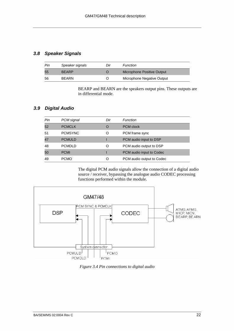
3.9 Digital Audio
Pin PCM signal Dir Function
52 PCMCLK O PCM clock
51 PCMSYNC O PCM frame sync
47 PCMULD I PCM audio input to DSP
48 PCMDLD O PCM audio output to DSP
50 PCMI I PCM audio input to Codec
49 PCMO O PCM audio output to Codec
The digital PCM audio signals allow the connection of a digital audiosource / receiver, bypassing the analogue audio CODEC processingfunctions performed within the module.
Figure 3.4 Pin connections to digital audio

GM47/GM48 Technical description
BA/SEM/MS 02:0004 Rev C 23
In the case where no external audio processing is performed, then it isnecessary to connect the following signals at the system connector:
PCMDLD and PCMIPCMULD and PCMO
Electrical characteristicsThe Dig. 2.75 V CMOS Output / Input electrical characteristics shallapply, with DGND as the reference.
PCM interface formatThe PCM format (for PCMULD and PCMDLD) shall follow a linearPCM data I/O format of an industry standard Texas Instrument DSP.It is the same format as the one used between the CODEC and theDSP. The DSP is the source of the bit clock PCMCLK and the framesynchronisation PCMSYNC. The data bits in PCMULD andPCMDLD shall be aligned so that the MSB in each word occurs onthe same clock edge.

GM47/GM48 Technical description
BA/SEM/MS 02:0004 Rev C 24
3.10 Serial Data
Pin Name Dir Description RS232 CCITTNº
41 TD I Serial data to module 103
42 RD O Serial data from module 104
39 RTS I Request To Send 105
40 CTS O Clear To Send 106
37 DTR I Data Terminal Ready 108.2
38 DCD O Data Carrier Detect 109
36 RI O Ring Indicator 125
45 TD2 I UART 2 Data Transmission
46 RD2 O UART 2 Data Reception
43 TD3 O UART 3 Data Transmission
44 RD3 I UART 3 Data Reception
The serial channels are used as asynchronous communication linksbetween an application system or accessory units connected to theModule. They consist of three UART's.
• UART 1 – This has full RS232 functionality except for the DSRsignal and is used for all on and off line communication.
• UART 2 – Used for interfacing to a GPS unit, downloadingsoftware and receiving logging information.
• UART 3 – RFU
The Dig. 2.75 V CMOS Output / Input electrical characteristics shallapply, with DGND as the reference. Extra relevant data is specifiedfor some of the signals.
The character format supported is, 1 start bit, 8 bit data, non-parityplus 1 stop bit, in total 10 bits per character.
Note : As stated in section 3.2.1 the module is unable to directlyinterface to a 3.3V micro processor.

GM47/GM48 Technical description
BA/SEM/MS 02:0004 Rev C 25
3.10.1 UART 1 (RS232) - RD, TD, RTS, CTS, DTR, DCD and RI
The UART1 signals form a 9 pin RS-232 (V.24) serial port, apartfrom the DSR (CCITT Nº 107) signal. DSR signal has been removedas it is usually connected to DTR in most systems.
The signal levels do not match the standard RS-232 (V.28) levels. Therelationship between the levels is shown in the table below
RS - 232 Level RD, TD RTS, CTS, DTR, DCD, RI 2.75 V CMOS Level
< - 3 V 1 OFF > 1.93
> + 3 V 0 ON < 0.80 V
Conversion between the 2.75V CMOS levels and the RS232 levelscan be achieved using a standard interface IC, such as the MaximIntegrated Products MAX3237.
3.10.2 Serial Data Signals - RD, TD
The default baud rate is 9.6 kbit/s, however higher bit rates up to 460kbit/s are supported and are set by the AT+IPR command. The UART1 starts at a rate of 9.6 kbit/s in standard AT mode or binary mode(First received data AT or binary will determine the operation mode).The GSM 07.10 multiplexing protocol is supported and is started oncommand, in this case bit rates up to 460 kbits/s are supported.
Serial Data From Module (RD)RD is an output used to send data on the UART 1 to the applicationsystem. This is a Dig. 2.75 CMOS Output and general characteristicsare applicable.
Parameter Limit
Application load resistance < 100 kΩ
Application load capacitance < 500 pF
Serial Data To Module (TD)TD is input (to the module) used by the application system to senddata on the UART 1 to the module. This is a Dig. 2.75 CMOS Inputand general characteristics are applicable.
Parameter Limit
Application driving impedance < 100 Ω
Input capacitance 1 nF
Input resistance (pull-up) 100 kΩ to 2.75 V
GM47/GM48 Technical description
BA/SEM/MS 02:0004 Rev C 26
3.10.3 Control Signals - RTS, CTS, DTR, DCD, RI
The control signals are active low, and hence when a standardinterface IC is used (such as MAX3237), then standard RS-232 levelsare obtained.
These signals together with DGND, RD and TD form a 9-pin RS-232data port (with the exception of the voltage levels and DSR).RTS and CTS shall be capable of transmitting at 1/10 of the datatransmission speed for data rates, up to 460 kbit/s. (Byte oriented flowcontrol mechanism).
Switching times for RTS and CTS
Parameter Limit
Time from Low to High level < 2 µs
Time from High to Low level < 2 µs
Request to Send (RTS)RTS is an input to the module. The signals on this circuit are used tocondition the DCE (the module when used for data transmissionpurposes) for data transmission. Default level is OFF, by internal pullup.
The exact behaviour of RTS is defined by the AT+IFC command.Software or hardware flow control can be selected. Hardware flowcontrol is the default.
This is a Dig. 2.75 CMOS Input and general characteristics areapplicable.
It is the duty of the application to pull RTS low (logic levels) torequest communications with the module. The module will respond byasserting CTS low and as such may be used as a notification as amodule status ready for communication.
Parameter Limit
Application driving impedance < 100 Ω
Input capacitance < 2 nF
Input resistance (pull-down) 100 kΩ to DGND

GM47/GM48 Technical description
BA/SEM/MS 02:0004 Rev C 27
Clear To Send (CTS)CTS is an output from the module. The signals on this circuit are usedto indicate that the DCE (the module when used for data transmissionpurposes) is ready to transmit data. Default level is high.The exact behaviour of CTS is defined by the AT+IFC command.Software or hardware flow control can be selected.
This is a Dig. 2.75 CMOS Output and general characteristics areapplicable.
Tip: if only software flow control is to be used it becomes necessaryto assert RTS low or to connect RTS to CTS at the module.
Parameter Limit
Application load capacitance < 500 pF
Application load resistance > 1 MΩ
Data Terminal Ready (DTR)DTR is an input to the module. Signals from the DTE on this circuitindicate the DTE is ready to transmit and receive data. DTR also actsas a hardware 'hang-up' so that calls are terminated if DTR is OFF(high).
Default level is ON (low). The exact behaviour of DTR is defined bythe AT&D command.
This is a Dig. 2.75 CMOS Input and general characteristics areapplicable.
Data Carrier Detect (DCD)DCD is an output from the module. An ON (low) signal shall indicatethat a valid carrier (data signal) is being received by the DCE(module). The exact behaviour of DCD is defined by the AT&Ccommand.
This is a Dig. 2.75 CMOS Output and general characteristics areapplicable.
Ring Indicator (RI)RI is an output from the module. An ON (low) signal indicates aringing signal is being received by the DCE (module).
This is a Dig. 2.75 CMOS Output and general characteristics areapplicable.
Note: DSR is not supported and is therefore considered permanentlyready for a module, therefore any DGND connection may be taken asDSR functionality.

GM47/GM48 Technical description
BA/SEM/MS 02:0004 Rev C 28
3.10.4 UART 2 - TD2, RD2
The UART 2 consists of a full duplex serial communication. Thisinvolves the transmission and reception lines.
The communication port shall work in one mode: Operation andMaintenance mode.
Operation and Maintenance mode shall work in addition with theSERVICE signal. On switching the module on, if SERVICE signal isactive then two events can happen. If no data is sent to the module,then the logger is activated. Otherwise, the module shall be ready tobe reprogrammed.
Timing and Electrical signal characteristics equal to UART 1 TD andRD, except for maximum baud rate that could be increased to 921kbps.
Transmitted Data 2 (TD2)TD2 is input (to the module) used by the application system to senddata on the UART 2 to the module.
The electrical characteristics shall be the same as TD.
Received Data 2 (RD2)RD2 is an output used to send data on the UART 2 to the applicationsystem.
The electrical characteristics shall be the same as RD.
3.10.5 UART 3 - TD3, RD3
The UART 3 consists of a full duplex serial communication. Thisinvolves the transmission and reception lines.
Timing and electrical signals characteristics equal to UART 1 TD andRD.
Transmitted Data 3 (TD3)TD3 is input (to the module) used by the application system to senddata on the UART 3 to the module.
The electrical characteristics shall be the same as TD.
Received Data 3 (RD3)

GM47/GM48 Technical description
BA/SEM/MS 02:0004 Rev C 29
RD is an output used to send data on the UART 3 to the applicationsystem.
The electrical characteristics shall be the same as RD.
3.11 SIM Card related signals
Parameter Mode Signal Min. Typ. Max. Unit
SIM supply Voltage 3 V SIMVCC 2.7 3.0 3.3 V
5 V 4.5 5.0 5.5 V
High Level Input Voltage(VIH)
3 V SIMDAT 2.1 3.0 V
5 V 3.5 5.0 V
Low Level Input Voltage(VIL)
3 V SIMDAT 0 0.9 V
5 V 0 1.5 V
High Level Output Voltage(VOH)
3 V SIMDAT 2.7 3.0 V
5 V 4.7 5.0 V
Low Level Output Voltage(VOL)
3 V SIMDAT 0 0.2 V
5 V 0 0.2 V
High Level Output Voltage(VOH)
3 V SIMCLK
SIMRST
2.4 3.0 V
5 V 4.4 5.0 V
Low Level Output Voltage(VOL)
3 V SIMCLK
SIMRST
0 0.35 V
5 V 0 0.3 V

GM47/GM48 Technical description
BA/SEM/MS 02:0004 Rev C 30
3.11.1 SIM Detection – SIM Presence
SIMDETECT is an input intended to be used to determine whether aSIM card has been inserted or removed in the external SIM cardholder. It shall be normally wired to the "Card Inserted Switch" of theexternal SIM card holder.
When left open an internal pull up resistor maintains the signal highand means ‘SIM card missing’ to the module. When pulled low themodule assumes a SIM card is inserted.
SIMDETECT is a digital CMOS 2.75 input with the followingcharacteristics.
Parameter Min. Typ. Max. Units
Pull-up resistance (at 2.75 V) 100 kΩ
Low Level Input Voltage (SIM inserted) 0.8 V
High Level Input Voltage (SIM missing) 1.93 5 V
Note : The module has been Type Approved with SIMpresence/detection implemented, to avoid extra testing when typeapproving the application this should be designed in.
3.12 Service/Programming
Pin Signal Description
58 SERVICE Flash programming voltage
This input shall be used as a programming voltage for the FlashMemory to initiate and it is also used as a signal to indicate to themodule that it should start outputting logging information.
Mode SERVICE Voltage (V) Drive Capacity
Min. Typ. Max.
Normal Operation 0.8 -
Service/enable programming 1.9 2.75 3.6 > 1 mA
Absolute maximum voltage 13.5 -

GM47/GM48 Technical description
BA/SEM/MS 02:0004 Rev C 31
3.13 Buzzer
Pin Signal Description
31 BUZZER Buzzer Output from module
This is an output signal which allows the application to use pre-programmed melodies or sounds. Typical use would involve atransistor buffer with a piezoelectric sounder.
The Dig. 2.75 V CMOS Output electrical characteristics shall apply,with DGND as the reference.
3.14 LED
Pin Signal Description
33 LED LED Output from module
This is an output signal which allows the use of an external LED. TheLED shall indicate different states within the module.
This signal is a Dig. 2.75 V CMOS output so general characteristicsare applicable. In order to connect a LED in the external applicationthe following scheme shall be followed.
The operation of the LED is hardcoded and is not controlled by thehost application.
Figure 3.5 Electrical connection for LED
GM47/GM48 Technical description
BA/SEM/MS 02:0004 Rev C 32
3.15 TX_ON - Burst Transmission
Pin Signal Dir Description
35 TX_ON O GSM module on transmission
The TX_ON is a digital signal output. This shall indicate that themodule is going to transmit the burst. Burst transmission is the timewhen a GSM transceiver unit.
Dig 2.75 CMOS Output so general electrical characteristics areapplicable.
3.16 Timestamp
Pin Signal Dir Description
32 TIMESTAMP O Global Positioning System Timestamp
TIMESTAMP is a Dig. 2.75 V CMOS Output electricalcharacteristics, with DGND as the reference.
Its main purpose is the A-GPS timestamp. As it is shown this is onlyapplicable when the Assisted GPS is implemented. In order to applythe assisted GPS performance not only MS implementation isnecessary but network side as well.
GM47/GM48 Technical description
BA/SEM/MS 02:0004 Rev C 33
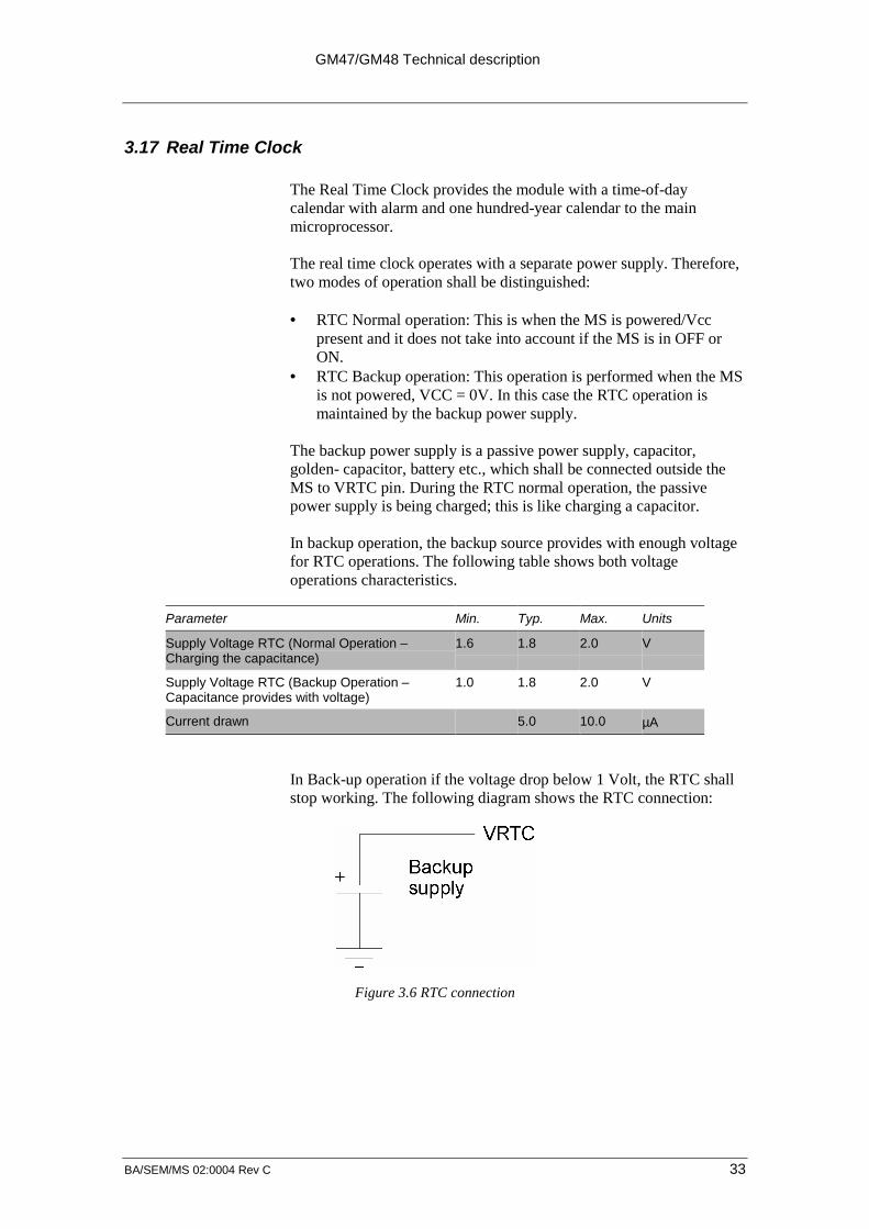
3.17 Real Time Clock
The Real Time Clock provides the module with a time-of-daycalendar with alarm and one hundred-year calendar to the mainmicroprocessor.
The real time clock operates with a separate power supply. Therefore,two modes of operation shall be distinguished:
• RTC Normal operation: This is when the MS is powered/Vccpresent and it does not take into account if the MS is in OFF orON.
• RTC Backup operation: This operation is performed when the MSis not powered, VCC = 0V. In this case the RTC operation ismaintained by the backup power supply.
The backup power supply is a passive power supply, capacitor,golden- capacitor, battery etc., which shall be connected outside theMS to VRTC pin. During the RTC normal operation, the passivepower supply is being charged; this is like charging a capacitor.
In backup operation, the backup source provides with enough voltagefor RTC operations. The following table shows both voltageoperations characteristics.
Parameter Min. Typ. Max. Units
Supply Voltage RTC (Normal Operation –Charging the capacitance)
1.6 1.8 2.0 V
Supply Voltage RTC (Backup Operation –Capacitance provides with voltage)
1.0 1.8 2.0 V
Current drawn 5.0 10.0 µA
In Back-up operation if the voltage drop below 1 Volt, the RTC shallstop working. The following diagram shows the RTC connection:
Figure 3.6 RTC connection
GM47/GM48 Technical description
BA/SEM/MS 02:0004 Rev C 34
4 Antenna Connector
The Antenna Connector is a hub for transmission of the RadioFrequency (RF) signals from the module to the external customer-supplied antenna. It is a MMCX connector that is mounted on thesurface of the module. Most dealers should be able to supply this typeof connector.
This table provides the electrical characteristics at the antennainterface.
Parameter Limit DescriptionNominal impedance 50 Ω (SWR < 2:1)
Output Power 2 Watt peak (Class 4) Extended GSM 900
1 Watt peak (Class 1) GSM 1800
Static Sensitivity Better than - 102 dBm Extended GSM 900
Better than - 102 dBm GSM 1800

GM47/GM48 Technical description
BA/SEM/MS 02:0004 Rev C 35
5 AT Command Summary
The AT standard is a line-oriented command language. "AT" is anabbreviation of ATtention and it is always used to start sending acommand line from a TE to the TA. TE stands for TerminalEquipment which is a computer of any size and TA stands forTerminal Adapter which is the modem part of the module.
The command line consists of a string of alphanumeric characters. It issent to the modem to instruct it to perform the commands specified bythe characters.
Functionality AT commands
CONTROL AND IDENTIFICATION
Subscriber Information AT+CNUM, AT+CIMI, AT*ESNU
Product & Release info AT+CGMI, AT+CGMM, AT+CGMR,AT+CGSN, AT*ESIR
Generic information & Settings AT, AT*, AT+CLAC, AT+GCAP, ATI,AT+CSCS, AT&F, AT&W, ATZ, AT+WS46,AT*E2SSN
CALL CONTROL
General call control ATA, ATD, ATL, ATH, ATP, ATT, AT+CHUP,AT+CMOD, AT+CVHU, AT+CR, AT+CRC,
DTMF AT+VTS
Data commands ATO, AT+CRLP
AUDIO CONTROL
Audio profile modification AT*E2EAMS
Audio profile manipulation AT*EALR, AT*EAMS, AT*EARS, AT*ELAM,AT*EMIR, AT*EMIC, AT*EXVC, AT*E2APR
NETWORK SERVICES
Alternate Line Service (ALS) AT*EALS, AT*ELIN, AT*ESLN
Customer Service Profile AT*ECSP
Call forwarding AT+CCFC, AT*EDIF
Calling/called number identification AT+CLIP, AT+CLIR, AT*EIPS
Preferred networks AT*EPNR, AT*EPNW
Advice of Charge AT+CACM, AT+CAMM, AT+CAOC,AT+CPUC
Calling cards AT*ESCN
Call hold, waiting & multiparty AT+CCWA, AT+CHLD
Operator selection AT+COPS

GM47/GM48 Technical description
BA/SEM/MS 02:0004 Rev C 36
Network registration AT+CREG
USSD AT+CUSD, AT+CSSN
Security & Locks AT+CLCK, AT+CPWD, AT+CPIN, AT*EPEE
SETTINGS
Restting AT*EMAR
Ring signal settings AT*ERIL, AT*ERIN, AT*ERIP, AT*ESIL,AT*ESMA, AT*ESMM, AT*ESOM
ME STATUS INFORMATION AT*ECAM, AT+CSQ, AT+CIND, AT+CPAS,AT+CMER
ERROR CONTROL AT+CMEE, AT+CEER
SMS & CB
Settings AT*ESTL, AT+CPMS, AT+CRES, AT+CSAS,AT+CSCA, AT+CSMS, AT+CNMI, AT+CSDH,AT+CSMP, AT+CGSMS
SMS-Command AT+CMGC
Read / write SMS AT+CMGD, AT+CMGW, AT+CMGL,AT+CMGR
Send SMS AT+CMGS, AT+CMSS
PHONEBOOK
Read / write / find AT+CPBS, AT+CPBR, AT+CPBW, AT+CPBF
Groups AT*EGIR, AT*ESAG, AT*ESCG, AT*ESDG,AT*ESDI, AT*ESGR
Personal Rings AT*EPRR, AT*EPRW
Settings AT*EPBM, AT*ESIA, AT*E2PBCS
CLOCK
Alarm AT+CALA, AT+CALD, AT+CAPD
Time & Date AT+CCLK, AT+CTZU, AT*EDST
INTERFACE COMMANDS
Flow control AT&C, AT&D, AT+ICF, AT+IFC, AT+IPR
S registers ATS0, ATS10, ATS2, ATS3, ATS4, ATS5,ATS6, ATS7, ATS8
Response control AT+ILRR, ATE, ATV, ATQ, AT+CSCS, ATX
07.10 MULTIPLEXING AT+CMUX
HSCSD AT+CHSR, AT+CHSU

GM47/GM48 Technical description
BA/SEM/MS 02:0004 Rev C 37
GPRS
PDP Context Activation AT+CGACT
Manual PDP Context Activation AT+CGANS
GPRS Attachment AT+CGATT
Enter Data State AT+CGDATA
Define PDP Context AT+CGDCONT
GPRS Event Reporting AT+CGEREP
Show PDP Address AT+CGPADDR
Quality of Service Profile (MINIMUMACCEPTABLE)
AT+CGQMIN
Quality of Service Profile (REQUESTED) AT+CGQREQ
GPRS Network registration Status AT+CGREG
Extension of ATD for GPRS ATD*
NETWORK INFORMATION
Cell information AT*E2CD
Engineering Mode AT*E2EMM
SIM APPLICATION TOOLKIT
Set Up Call AT*E2STKC
Display Text AT*E2STKD
Get Inkey AT*E2STKG
Get Input AT*E2STKI
Select Item AT*E2STKL
Set Up Menu AT*E2STKM
Envelope (Menu Selection) AT*E2STKN
Application Toolkit Settings AT*E2STKS
GM47/GM48 Technical description
BA/SEM/MS 02:0004 Rev C 38
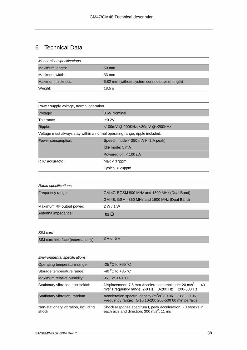
6 Technical Data
Mechanical specifications
Maximum length: 50 mm
Maximum width: 33 mm
Maximum thickness: 6.82 mm (without system connector pins length)
Weight: 18,5 g
Power supply voltage, normal operation
Voltage: 3.6V Nominal
Tolerance ±0.2V
Ripple: <100mV @ 200KHz, <20mV @>200KHz
Voltage must always stay within a normal operating range, ripple included.
Power consumption: Speech mode < 250 mA (< 2 A peak)
Idle mode: 5 mA
Powered off: < 100 µA
RTC accuracy: Max < 37ppm
Typical < 20ppm
Radio specifications
Frequency range: GM 47: EGSM 900 MHz and 1800 MHz (Dual Band)
GM 48: GSM 850 MHz and 1900 MHz (Dual Band)
Maximum RF output power: 2 W / 1 W
Antenna impedance: 50 Ω
SIM card
SIM card interface (external only) 3 V or 5 V
Environmental specifications
Operating temperature range: -25 0C to +55 0C
Storage temperature range: -40 0C to +85 0C
Maximum relative humidity: 95% at +40 0C
Stationary vibration, sinusoidal: Displacement: 7.5 mm Acceleration amplitude: 20 m/s2 40m/s2 Frequency range: 2-8 Hz 8-200 Hz 200-500 Hz
Stationary vibration, random Acceleration spectral density (m2/s2): 0.96 2.88 0.96Frequency range: 5-10 10-200 200-500 60 min per/axis
Non-stationary vibration, includingshock
Shock response spectrum I, peak acceleration: - 3 shocks ineach axis and direction: 300 m/s2, 11 ms

GM47/GM48 Technical description
BA/SEM/MS 02:0004 Rev C 39
Shock response spectrum II, peak acceleration: - 3 shocks ineach axis and direction: 1000 m/s2, 6 ms
Bump: Acceleration 250 m/s2
Free fall transportation: 1.2 m
Rolling pitching transportation: Angle: ±35 degrees, period: 8s
Static load: 10 kPa
Low air pressure/high air pressure: 70 kPa / 106 kPa
Storage
SMS Storage capacity 40 in ME
In addition the unit can handle as many SMS as the SIM canstore (SIM dependent).
Phone book capacity 100
DAC
Parameter Value Units
Resolution 8 bit
Output voltage swing for Code=00HEX 0.138 ± 0.1 V
Output voltage swing for Code=FFHEX 2.61 ± 0.2 V
Nominal Step Size 9.668 ± 0.1 mV
Linear Code Range 8-247 (8H-F7H) LSB
Absolute Error during Linear Range ±100 mV
Conversion Speed <100 µs
ADC
Parameter Value Units
Resolution 8 bit
Input voltage for Code=00H 0.01 ± 0.01 V
Input voltage for Code=FFH 2.75 ± 0.1 V
Nominal Step Size 10.742 mV
Accuracy ±3 LSB
Input Impedance >1 MΩ
Conversion Time to within 0.5bit <100 µs

GM47/GM48 Technical description
BA/SEM/MS 02:0004 Rev C 40
7 Contact details
To contact customer support please use the details below.
Customer SupportMaplewood BuildingChineham Business ParkBasingstokeRG24 8YB
E mail :
[email protected]@sonyericsson.com