glucose meter flash mcu with lcd - holtek · 2019-11-07 · rev. 1.20 8 november 01, 2019 rev. 1.20...
TRANSCRIPT

Glucose Meter Flash MCU with LCD
BH67F2480
Revision: V1.20 Date: November 01, 2019

Rev. 1.20 2 November 01, 2019 Rev. 1.20 3 November 01, 2019
BH67F2480Glucose Meter Flash MCU with LCD
BH67F2480Glucose Meter Flash MCU with LCD
Table of ContentsFeatures ............................................................................................................ 7
CPU Features ......................................................................................................................... 7Peripheral Features ................................................................................................................. 7
General Description ......................................................................................... 8Block Diagram .................................................................................................. 9Pin Assignment .............................................................................................. 10Pin Description .............................................................................................. 12Absolute Maximum Ratings .......................................................................... 16D.C. Electrical Characteristics ...................................................................... 17
Operating Voltage Characteristics ......................................................................................... 17Operating Current Characteristics ......................................................................................... 17Standby Current Characteristics ........................................................................................... 18
A.C. Electrical Characteristics ...................................................................... 19Low Speed Internal Oscillator Characteristics – LIRC .......................................................... 19Operating Frequency Characteristic Curves ......................................................................... 19System Start Up Time Characteristics .................................................................................. 20
Input/Output Characteristics ........................................................................ 20Memory Characteristics ................................................................................ 21LVR/LVD Electrical Characteristics .............................................................. 22OVP Characteristics ...................................................................................... 22LCD Characteristics ...................................................................................... 23Analog Front End Circuit Characteristics ................................................... 24
OPA Electrical Characteristics ............................................................................................... 24Internal Reference Voltage Characteristics ........................................................................... 24Analog Switch Electrical Characteristics ............................................................................... 2412-bit D/A Converter Electrical Characteristics ..................................................................... 24A/D Converter Electrical Characteristics ............................................................................... 25
Power-on Reset Characteristics ................................................................... 25System Architecture ...................................................................................... 26
Clocking and Pipelining ......................................................................................................... 26Program Counter ................................................................................................................... 27Stack ..................................................................................................................................... 27Arithmetic and Logic Unit – ALU ........................................................................................... 28
Flash Program Memory ................................................................................. 29Structure ................................................................................................................................ 29Special Vectors ..................................................................................................................... 29Look-up Table ....................................................................................................................... 29Table Program Example ........................................................................................................ 30In Circuit Programming – ICP ............................................................................................... 31

Rev. 1.20 2 November 01, 2019 Rev. 1.20 3 November 01, 2019
BH67F2480Glucose Meter Flash MCU with LCD
BH67F2480Glucose Meter Flash MCU with LCD
On-Chip Debug Support – OCDS ......................................................................................... 32In Application Programming – IAP ........................................................................................ 32
Data Memory .................................................................................................. 47Structure ................................................................................................................................ 47Data Memory Addressing ...................................................................................................... 48General Purpose Data Memory ............................................................................................ 48Special Purpose Data Memory ............................................................................................. 48
Special Function Register Description ........................................................ 50Indirect Addressing Registers – IAR0, IAR1, IAR2 ............................................................... 50Memory Pointers – MP0, MP1L, MP1H, MP2L, MP2H ......................................................... 50Program Memory Bank Pointer – PBP .................................................................................. 51Accumulator – ACC .............................................................................................................. 52Program Counter Low Register – PCL ................................................................................. 52Look-up Table Registers – TBLP, TBHP, TBLH .................................................................... 52Status Register – STATUS ................................................................................................... 53
EEPROM Data Memory .................................................................................. 55EEPROM Data Memory Structure ........................................................................................ 55EEPROM Registers .............................................................................................................. 55Reading Data from the EEPROM ......................................................................................... 57Writing Data to the EEPROM ................................................................................................ 57Write Protection ..................................................................................................................... 57EEPROM Interrupt ................................................................................................................ 57Programming Considerations ................................................................................................ 58
Oscillators ...................................................................................................... 59Oscillator Overview ............................................................................................................... 59System Clock Configurations ................................................................................................ 59External Crystal/Ceramic Oscillator – HXT ........................................................................... 60Internal High Speed RC Oscillator – HIRC ........................................................................... 61External 32.768kHz Crystal Oscillator – LXT ........................................................................ 61Internal 32kHz Oscillator – LIRC ........................................................................................... 62
Operating Modes and System Clocks ......................................................... 62System Clocks ...................................................................................................................... 62System Operation Modes ...................................................................................................... 63Control Registers .................................................................................................................. 64Operating Mode Switching .................................................................................................... 67Standby Current Considerations ........................................................................................... 71Wake-up ................................................................................................................................ 71
Watchdog Timer ............................................................................................. 72Watchdog Timer Clock Source .............................................................................................. 72Watchdog Timer Control Register ......................................................................................... 72Watchdog Timer Operation ................................................................................................... 73
Reset and Initialisation .................................................................................. 74Reset Functions .................................................................................................................... 74Reset Initial Conditions ......................................................................................................... 77

Rev. 1.20 4 November 01, 2019 Rev. 1.20 5 November 01, 2019
BH67F2480Glucose Meter Flash MCU with LCD
BH67F2480Glucose Meter Flash MCU with LCD
Input/Output Ports ......................................................................................... 82Pull-high Resistors ................................................................................................................ 82Port A Wake-up ..................................................................................................................... 83I/O Port Control Registers ..................................................................................................... 83Source Current Selection ...................................................................................................... 84Pin-shared Functions ............................................................................................................ 86I/O Pin Structures .................................................................................................................. 93Programming Considerations ................................................................................................ 93
Timer Modules – TM ...................................................................................... 94Introduction ........................................................................................................................... 94TM Operation ........................................................................................................................ 94TM Clock Source ................................................................................................................... 95TM Interrupts ......................................................................................................................... 95TM External Pins ................................................................................................................... 95Programming Considerations ................................................................................................ 96
Standard Type TM – STM .............................................................................. 97Standard TM Operation ......................................................................................................... 97Standard Type TM Register Description ............................................................................... 98Standard Type TM Operation Modes .................................................................................. 102
Periodic Type TM – PTM ...............................................................................111Periodic TM Operation .........................................................................................................111Periodic Type TM Register Description ...............................................................................111Periodic Type TM Operating Modes ....................................................................................115
Internal Reference Voltage Generator ....................................................... 124Internal Reference Voltage Register Description ................................................................ 124
Digital to Analog Converter – DAC ............................................................. 125D/A Converter Registers ..................................................................................................... 125
Operational Amplifier – OPA ....................................................................... 127OPA Register Description .................................................................................................... 127Input Offset Calibration ....................................................................................................... 129
Analog to Digital Converter – ADC ............................................................. 130A/D Converter Overview ..................................................................................................... 130A/D Converter Register Description .................................................................................... 131A/D Converter Operation .................................................................................................... 134A/D Converter Reference Voltage ....................................................................................... 135A/D Converter Input Signals ................................................................................................ 135Conversion Rate and Timing Diagram ................................................................................ 136Summary of A/D Conversion Steps ..................................................................................... 136Programming Considerations .............................................................................................. 137A/D Conversion Function .................................................................................................... 137A/D Conversion Programming Examples ............................................................................ 138
16-bit Multiplication Division Unit – MDU .................................................. 140MDU Registers .................................................................................................................... 140MDU Operation ................................................................................................................... 141

Rev. 1.20 4 November 01, 2019 Rev. 1.20 5 November 01, 2019
BH67F2480Glucose Meter Flash MCU with LCD
BH67F2480Glucose Meter Flash MCU with LCD
Over Voltage Protection – OVP ................................................................... 142Over Voltage Protection Operation ..................................................................................... 143Over Voltage Protection Control Registers ......................................................................... 143Input Offset Calibration ....................................................................................................... 144
Serial Interface Module – SIM ..................................................................... 145SPI Interface ....................................................................................................................... 145I2C Interface ........................................................................................................................ 152
Serial Peripheral Interface – SPIA .............................................................. 162SPIA Interface Operation .................................................................................................... 162SPIA Registers .................................................................................................................... 163SPIA Communication .......................................................................................................... 165SPIA Bus Enable/Disable .................................................................................................... 167SPIA Operation Steps ......................................................................................................... 168Error Detection .................................................................................................................... 169
UART Interfaces – UART0 & UART1 .......................................................... 170UARTn External Pins .......................................................................................................... 171UARTn Data Transfer Scheme ........................................................................................... 171UARTn Status and Control Registers ................................................................................. 171Baud Rate Generator .......................................................................................................... 177UARTn Setup and Control .................................................................................................. 177UARTn Transmitter ............................................................................................................. 178UARTn Receiver ................................................................................................................. 180Managing Receiver Errors .................................................................................................. 181UARTn Interrupt Structure .................................................................................................. 182UARTn Power Down and Wake-up ..................................................................................... 183
LCD Driver .................................................................................................... 184LCD Display Memory .......................................................................................................... 184LCD Clock Source .............................................................................................................. 185LCD Registers ..................................................................................................................... 185LCD Voltage Source and Biasing ........................................................................................ 187LCD Reset Status ............................................................................................................... 191LCD Driver Output ............................................................................................................... 191Programming Considerations .............................................................................................. 200
Low Voltage Detector – LVD ....................................................................... 201LVD Register ....................................................................................................................... 201LVD Operation ..................................................................................................................... 202
Interrupts ...................................................................................................... 203Interrupt Registers ............................................................................................................... 203Interrupt Operation .............................................................................................................. 208External Interrupts ............................................................................................................... 210A/D Converter Interrupt ....................................................................................................... 210Over Voltage Protection Interrupt ........................................................................................ 210Time Base Interrupts ............................................................................................................211UART Interface Interrupts ................................................................................................... 212

Rev. 1.20 6 November 01, 2019 Rev. 1.20 7 November 01, 2019
BH67F2480Glucose Meter Flash MCU with LCD
BH67F2480Glucose Meter Flash MCU with LCD
Serial Interface Module Interrupt ......................................................................................... 212SPIA Interrupt ..................................................................................................................... 213Multi-function Interrupts ....................................................................................................... 213LVD Interrupt ....................................................................................................................... 213EEPROM Interrupt .............................................................................................................. 213Timer Module Interrupts ...................................................................................................... 214Interrupt Wake-up Function ................................................................................................. 214Programming Considerations .............................................................................................. 214
Configuration Options ................................................................................. 215Application Circuits ..................................................................................... 215Instruction Set .............................................................................................. 216
Introduction ......................................................................................................................... 216Instruction Timing ................................................................................................................ 216Moving and Transferring Data ............................................................................................. 216Arithmetic Operations .......................................................................................................... 216Logical and Rotate Operation ............................................................................................. 217Branches and Control Transfer ........................................................................................... 217Bit Operations ..................................................................................................................... 217Table Read Operations ....................................................................................................... 217Other Operations ................................................................................................................. 217
Instruction Set Summary ............................................................................ 218Table Conventions ............................................................................................................... 218Extended Instruction Set ..................................................................................................... 220
Instruction Definition ................................................................................... 222Extended Instruction Definition ........................................................................................... 231
Package Information ................................................................................... 23864-pin LQFP (7mm×7mm) Outline Dimensions .................................................................. 23980-pin LQFP (10mm×10mm) Outline Dimensions .............................................................. 240

Rev. 1.20 6 November 01, 2019 Rev. 1.20 7 November 01, 2019
BH67F2480Glucose Meter Flash MCU with LCD
BH67F2480Glucose Meter Flash MCU with LCD
Features
CPU Features• Operating Voltage
♦ fSYS = 4MHz: 2.2V~5.5V ♦ fSYS = 8MHz: 2.2V~5.5V ♦ fSYS = 12MHz: 2.7V~5.5V ♦ fSYS = 16MHz: 3.3V~5.5V
• Up to 0.25μs instruction cycle with 16MHz system clock at VDD=5V
• Power down and wake-up functions to reduce power consumption
• Oscillator types: ♦ External High Speed Crystal – HXT ♦ External Low Speed 32.768kHz Crystal – LXT ♦ Internal High Speed 4/8/12MHz RC – HIRC ♦ Internal Low Speed 32kHz RC – LIRC
• Fully integrated internal oscillators require no external components
• Multi-mode operation: FAST, SLOW, IDLE and SLEEP
• All instructions executed in 1~3 instruction cycles
• Table read instructions
• 115 powerful instructions
• 12-level subroutine nesting
• Bit manipulation instruction
Peripheral Features• Flash Program Memory: 48K×16
• RAM Data Memory: 1024×8
• True EEPROM Memory: 64×8
• Watchdog Timer function
• In Application Programming – IAP
• 46 bidirectional I/O lines
• Programmable I/O port source current for LED applications
• 4 pin-shared external interrupts
• Multiple Timer Modules for time measure, input capture, compare match output, PWM output or single pulse output function
♦ 1 Standard type 16-bit Timer Module – STM ♦ 3 Periodic type 10-bit Timer Modules – PTM0~PTM2
• Dual Time-Base functions for generation of fixed time interrupt signals
• Glucose Meter AFE ♦ 6 external channel 12-bit resolution A/D Converter ♦ Internal Reference Voltage Generator ♦ 12-bit D/A Converter ♦ 2 internal Operational Amplifiers

Rev. 1.20 8 November 01, 2019 Rev. 1.20 9 November 01, 2019
BH67F2480Glucose Meter Flash MCU with LCD
BH67F2480Glucose Meter Flash MCU with LCD
• Over Voltage Protection function with interrupt
• Serial Interface Module includes SPI and I2C interfaces
• Single Serial Peripheral Interface – SPIA
• Dual fully-duplex Universal Asynchronous Receiver and Transmitter Interfaces – UART0 and UART1
• 16-bit Multiplication Division Unit – MDU
• LCD Driver function ♦ SEGs × COMs: 48×4, 46×6 or 44×8 ♦ Duty type: 1/4 duty, 1/6 duty or 1/8 duty ♦ Bias level: 1/3 bias or 1/4 bias ♦ Bias type: R type or C type ♦ Waveform type: type A or type B
• Low Voltage Reset function
• Low Voltage Detect function
• Package types: 64/80-pin LQFP
General DescriptionThe BH67F2480 is a Flash Memory A/D type 8-bit high performance RISC architecture microcontroller, specifically designed for Glucose Meter with LCD display applications. Offering users the convenience of Flash Memory multi-programming features, this device also includes a wide range of functions and features. Other memory includes an area of RAM Data Memory as well as an area of true EEPROM memory for storage of non-volatile data such as serial numbers, calibration data etc. By using the In Application Programming technology, users have a convenient means to directly store their measured data in the Flash Program Memory as well as having the ability to easily update their application programs.
Analog features include a multi-channel 12-bit A/D converter and two internal operational amplifiers. Multiple and extremely flexible Timer Modules provide timing, pulse generation and PWM generation functions. Communication with the outside world is catered for by including fully integrated SPI, I2C and UART interface functions, some popular interfaces which provide designers with a means of easy communication with external peripheral hardware. Protective features such as an internal Watchdog Timer, Low Voltage Reset and Low Voltage Detector coupled with excellent noise immunity and ESD protection ensure that reliable operation is maintained in hostile electrical environments.
A full choice of external, internal and high and low oscillator functions are provided including two fully integrated system oscillators which require no external components for their implementation. The ability to operate and switch dynamically between a range of operating modes using different clock sources gives users the ability to optimise microcontroller operation and minimise power consumption.
With regard to Glucose Meter applications, the device has integrated many of the functions required by these products. These include functions such as Internal Reference Voltage generator, 12-bit D/A Converter, Over Voltage Protection, Multiplication/Division Unit, LCD driver function etc. The inclusion of flexible I/O programming features, Time-Base functions along with many other features ensure that the device will be highly capable of providing MCU solutions for Glucose Meter applications which include an LCD display.

Rev. 1.20 8 November 01, 2019 Rev. 1.20 9 November 01, 2019
BH67F2480Glucose Meter Flash MCU with LCD
BH67F2480Glucose Meter Flash MCU with LCD
Block Diagram
Interrupt Controller
Bus
MU
X
SYSCLK
Reset Circuit
LVR
Stack12-Level
RAM1024 × 8
ROM48K × 16
EEPROM64 × 8
LVD
HIRC4/8/12MHz
LIRC32kHz
Pin-SharedFunction
INT0~INT3
Pin-SharedWith Port A & B
Time Bases
HXT
LXT
Pin-SharedWith Port A
XT1XT2
OSC1OSC2
HT8 MCU Core
Clock System
Timers
Digital Peripherals
I/O
Analog Peripherals
MU
X
AN0~AN5
Pin-SharedWith Port A & C
OP1S1OP1S2
Analog to Digital Converter
OP1S0
VDACO
Pin-SharedWith Port A & B & D & E & F & G
LCD
OP2O
Internal Reference Voltage Generator
DACVREF
+OPA
_
12-bit DACOP1N
OP1O
DACO
+OPA
_ OP2N
Pin-SharedWith Port B
OP2O
Pin-SharedWith Port B
UART
OP1S1
OP1S2
OP1S0
SEG4~19
COM0~4LCDDriver
LCD RAM
SPIA
SEG0~3, SEG20~46
COM5~7
IAP
VREF
Pin-SharedWith Port A
VDD
VDACVREF
: SIM including SPI & I2C
SIM
MDUWatchdogTimer
Port A Driver PA0~PA7
PB0~3, PB5~7Port B Driver
PC0~PC5Port C Driver
PD0~PD5Port D Driver
PE0~PE7Port E Driver
PF0~PF7Port F Driver
PG0~PG2Port G Driver
: Pin-Shared Node
V2 V2
PLCD VPLCD
VMAX VMAX
V1 V1
SW1
SW2
SW0
12-bit ADC
VDD VDD
VSS VSS

Rev. 1.20 10 November 01, 2019 Rev. 1.20 11 November 01, 2019
BH67F2480Glucose Meter Flash MCU with LCD
BH67F2480Glucose Meter Flash MCU with LCD
Pin Assignment
PC1/AN
3/PTCK1
PC3/AN
1/PTCK2
PC0/AN
2/PTP1/PTP1I
PA0/XT1/PTP0/PTP0I/ICPD
A/OC
DSD
AVSS
PC2/AN
0/VREF/PTP2/PTP2I
PA2/XT2/PTCK0/IC
PCK/O
CD
SCK
PB2/INT2/SCS/SCKA/SEG39PB3/INT3/SDO/SDIA/SEG38
SEG18SEG19PF0/SEG20PF1/SEG21
PD4/STP/SEG36PD5/OVPI/SEG37OP1O
OP1S2OP1N
OP1S0OP1S1
PC4/AN4/SCSA/RX1
PB7/VGDACO
PC5/AN5/SDOA/TX1
PLCDDACVREF
PG0/C1/SEG45PG1/C2/SEG46
PG2/V2/SEG
47VM
AXV1
VDD
VSS
CO
M1
CO
M2
CO
M3
CO
M0
PA5/TX0/SCKA/STPI/SEG
44PA4/O
SC1/SC
SA/PTP2/PTP2I
PA1/INT0/LVD
IN/O
VPVR/PTP0B/STC
KVD
D
PB1/INT1/STPB/O
VPI/SEG40
PA6/RX0/SD
IA/STCK/SEG
43
PB0/SCK/SC
L/OVPI/SEG
41PA7/SD
I/SDA/PTC
K2/OVPI/SEG
42
PA3/OSC
2/SDO
A/PTP1/PTP1I
SEG4
SEG5
S EG7
S EG6
PD0/SEG
0 /CO
M4
P D1/SEG
1/ CO
M5
P D2/SEG
2/CO
M6
PD3/SEG
3/CO
M7
SEG17SEG16
PF2/SEG22PF3/SEG23PF4/SEG24PF5/SEG25PF6/SEG26PF7/SEG27
PB6/OP2OPB5/OP2N
BH67F2480/BH67V248064 LQFP-A
12345678910111213
20 21 22 23 24 25 26 27 28
6061626364
29 30 31 32
5253545556575859
141516
434445464748
36373839404142
333435
17 18 19
495051

Rev. 1.20 10 November 01, 2019 Rev. 1.20 11 November 01, 2019
BH67F2480Glucose Meter Flash MCU with LCD
BH67F2480Glucose Meter Flash MCU with LCD
PC1/AN
3/PTCK1
PC3/AN
1/PTCK2
PC0/AN
2/PTP1/PTP1I
PA0/XT1/PTP0/PTP0I/ICPD
A/OC
DSD
AVSS
PC2/AN
0/VREF/PTP2/PTP2I
PA2/XT2/PTCK0/IC
PCK/O
CD
SCK
PB2/INT2/SC
S/SCKA/SEG
39PB3/IN
T3/SDO
/SDIA/SEG
38OP1O
OP1S2OP1N
OP1S0OP1S1
PC4/AN4/SCSA/RX1PC5/AN5/SDOA/TX1
PA5/TX0/SCKA/STPI/SEG
44PA4/O
SC1/SC
SA/PTP2/PTP2I
PA1/INT0/LVD
IN/O
VPVR/PTP0B/STC
KVD
D
PB1/INT1/STPB/O
VPI/SEG40
PA6/RX0/SD
IA/STCK/SET43
PB0/SCK/SC
L/OVPI/SEG
41PA7/SD
I/SDA/PTC
K2/OVPI/SEG
42
PA3/OSC
2/SDO
A/PTP1/PTP1IBH67F2480/BH67V2480
80 LQFP-APB7/VG
DACO
PLCDDACVREF
PG0/C1/SEG45PG1/C2/SEG46
PG2/V2/SEG47VMAX
V1
VDDC
OM
1C
OM
0VSS
PB6/OP2OPB5/OP2N
CO
M2
CO
M3
S EG4
SE G5
SEG7
SEG6
PD0/SEG
0/CO
M4
P D1/SEG
1/ CO
M5
PD2/SEG
2/CO
M6
PD3/ SEG
3/CO
M7
SEG17SEG16
SEG8
SEG9
SEG11
SE G10
SEG12
SEG13
SE G15
SEG14
SEG18SEG19PF0/SEG20PF1/SEG21
PD4/STP/SEG
36PD
5/OVPI/SEG
37
PF2/SEG22PF3/SEG23PF4/SEG24PF5/SEG25PF6/SEG26PF7/SEG27PE0/SEG28PE1/SEG29PE2/SEG30PE3/SEG31PE4/SEG32PE5/SEG33PE6/SEG34PE7/SEG35
47464544434241
1234567891011121314151617181920
21 22 23 24 25 26 27 28 29 30 31 32 33 34 35 36 3738 39 40
80 79 78 77 76 75 74 73 72 71 70 69 68 67 66 65 6463 62 6160595857565554535251504948
Note: 1. If the pin-shared pin functions have multiple outputs, the desired pin-shared function is determined by the corresponding software control bits.
2. The OCDSDA and OCDSCK pins are supplied as the OCDS dedicated pins and as such only available for the BH67V2480 device which is the OCDS EV chip for the BH67F2480 device.
3. For less pin-count package types there will be unbonded pins which should be properly configured to avoid unwanted current consumption resulting from floating input conditions. Refer to the “Standby Current Considerations” and “Input/Output Ports” sections.

Rev. 1.20 12 November 01, 2019 Rev. 1.20 13 November 01, 2019
BH67F2480Glucose Meter Flash MCU with LCD
BH67F2480Glucose Meter Flash MCU with LCD
Pin DescriptionWith the exception of power and some LCD COM and SEG pins, all pins on the device can be referenced by its Port name, e.g. PA0, PA1 etc., which refer to the digital I/O function of the pins. However these Port pins are also shared with other functions such as the Analog to Digital Converter, Timer Modules etc. The function of each pin is listed in the following table, however the details behind how each pin is configured is contained in other sections of the datasheet.
Note that the pin description refers to the largest package size, as a result some pins may not exist on smaller package types.
Pin Name Function OPT I/T O/T Description
PA0/XT1/PTP0/PTP0I/ICPDA/OCDSDA
PA0PAPUPAWUPAS0
ST CMOS General purpose I/O. Register enabled pull-up and wake-up
XT1 PAS0 LXT — LXT oscillator pinPTP0 PAS0 — CMOS PTM0 output
PTP0I PAS0IFS0 ST — PTM0 capture input
ICPDA — ST CMOS ICP data/address pinOCDSDA — ST CMOS OCDS data/address pin, for EV chip only.
PA1/INT0/LVDIN/OVPVR/PTP0B/STCK
PA1PAPUPAWUPAS0
ST CMOS General purpose I/O. Register enabled pull-up and wake-up
INT0PAS0
INTEGINTC0
ST — External interrupt 0 input
LVDIN PAS0 AN — LVD inputOVPVR PAS0 AN — OVP reference voltage inputPTP0B PAS0 — CMOS PTM0 inverting output
STCK PAS0IFS0 ST — STM clock input
PA2/XT2/PTCK0/ICPCK/OCDSCK
PA2PAPUPAWUPAS0
ST CMOS General purpose I/O. Register enabled pull-up and wake-up
XT2 PAS0 — LXT LXT oscillator pinPTCK0 PAS0 ST — PTM0 clock inputICPCK — ST — ICP clock pin
OCDSCK — ST — OCDS clock pin, for EV chip only
PA3/OSC2/SDOA/PTP1/PTP1I
PA3PAPUPAWUPAS0
ST CMOS General purpose I/O. Register enabled pull-up and wake-up
OSC2 PAS0 — HXT HXT oscillator pinSDOA PAS0 — CMOS SPIA serial data outputPTP1 PAS0 — CMOS PTM1 output
PTP1I PAS0IFS0 ST — PTM1 capture input

Rev. 1.20 12 November 01, 2019 Rev. 1.20 13 November 01, 2019
BH67F2480Glucose Meter Flash MCU with LCD
BH67F2480Glucose Meter Flash MCU with LCD
Pin Name Function OPT I/T O/T Description
PA4/OSC1/SCSA/PTP2/PTP2I
PA4PAPUPAWUPAS1
ST CMOS General purpose I/O. Register enabled pull-up and wake-up
OSC1 PAS1 HXT — HXT oscillator pin
SCSA PAS1IFS1 ST CMOS SPIA slave select
PTP2 PAS1 — CMOS PTM2 output
PTP2I PAS1IFS0 ST — PTM2 capture input
PA5/TX0/SCKA/STPI/SEG44
PA5PAPUPAWUPAS1
ST CMOS General purpose I/O. Register enabled pull-up and wake-up
TX0PAS1
U0CR1U0CR2
— CMOS UART0 data transmit pin
SCKA IFS1PAS1 ST CMOS SPIA serial clock input
STPI PAS1 ST — STM capture inputSEG44 PAS1 — SEG LCD segment output
PA6/RX0/SDIA/STCK/SEG43
PA6PAPUPAWUPAS1
ST CMOS General purpose I/O. Register enabled pull-up and wake-up
RX0PAS1
U0CR1U0CR2
ST — UART0 data receive pin
SDIA PAS1IFS1 ST — SPIA serial data input
STCK PAS1IFS0 ST — STM clock input
SEG43 PAS1 — SEG LCD segment output
PA7/SDI/SDA/PTCK2/OVPI/SEG42
PA7PAPUPAWUPAS1
ST CMOS General purpose I/O. Register enabled pull-up and wake-up
SDI PAS1 ST — SIM SPI serial data inputSDA PAS1 ST NMOS SIM I2C data line
PTCK2 IFS0PAS1 ST — PTM2 clock input
OVPI PAS1 AN — OVP signal inputSEG42 PAS1 — SEG LCD segment output
PB0/SCK/SCL/OVPI/SEG41
PB0 PBPUPBS0 ST CMOS General purpose I/O. Register enabled pull-up
SCK PBS0 ST CMOS SIM SPI serial clockSCL PBS0 ST NMOS SIM I2C clock lineOVPI PBS0 AN — OVP signal input
SEG41 PBS0 — SEG LCD segment output
PB1/INT1/STPB/OVPI/SEG40
PB1 PBPUPBS0 ST CMOS General purpose I/O. Register enabled pull-up
INT1PBS0INTEGINTC0
ST — External interrupt 1 input
STPB PBS0 — CMOS STM inverting outputOVPI PBS0 AN — OVP signal input
SEG40 PBS0 — SEG LCD segment output

Rev. 1.20 14 November 01, 2019 Rev. 1.20 15 November 01, 2019
BH67F2480Glucose Meter Flash MCU with LCD
BH67F2480Glucose Meter Flash MCU with LCD
Pin Name Function OPT I/T O/T Description
PB2/INT2/SCS/SCKA/SEG39
PB2 PBPUPBS0 ST CMOS General purpose I/O. Register enabled pull-up
INT2PBS0INTEGINTC2
ST — External interrupt 2 input
SCS PBS0 ST CMOS SIM SPI slave chip select
SCKA IFS1PBS0 ST CMOS SPIA serial clock
SEG39 PBS0 — SEG LCD segment output
PB3/INT3/SDO/SDIA/SEG38
PB3 PBPUPBS0 ST CMOS General purpose I/O. Register enabled pull-up
INT3PBS0INTEGINTC2
ST — External interrupt 3 input
SDO PBS0 — CMOS SIM SPI serial data output
SDIA PBS0IFS1 ST — SPIA serial data input
SEG38 PBS0 — SEG LCD segment output
PB5/OP2NPB5 PBPU
PBS1 ST CMOS General purpose I/O. Register enabled pull-up
OP2N PBS1 AN — OPA2 negative input
PB6/OP2OPB6 PBPU
PBS1 ST CMOS General purpose I/O. Register enabled pull-up
OP2O PBS1 — AN OPA2 output
PB7/VGPB7 PBPU
PBS1 ST CMOS General purpose I/O. Register enabled pull-up
VG PBS1 AN — Virtual Ground
PC0/AN2/PTP1/PTP1I
PC0 PCPUPCS0 ST CMOS General purpose I/O. Register enabled pull-up
AN2 PCS0 AN — A/D Converter external input channel 2PTP1 PCS0 — CMOS PTM1 output
PTP1I IFS0PCS0 ST — PTM1 capture input
PC1/AN3/PTCK1
PC1 PCPUPCS0 ST CMOS General purpose I/O. Register enabled pull-up
AN3 PCS0 AN — A/D Converter external input channel 3PTCK1 PCS0 ST — PTM1 clock input
PC2/AN0/VREF/PTP2/PTP2I
PC2 PCPUPCS0 ST CMOS General purpose I/O. Register enabled pull-up
AN0 PCS0 AN — A/D Converter external input channel 0VREF PCS0 AN — A/D Converter external reference voltage inputPTP2 PCS0 — CMOS PTM2 output
PTP2I IFS0PCS0 ST — PTM2 capture input
PC3/AN1/PTCK2
PC3 PCPUPCS0 ST CMOS General purpose I/O. Register enabled pull-up
AN1 PCS0 AN — A/D Converter external input channel 1
PTCK2 PCS0IFS0 ST — PTM2 clock input

Rev. 1.20 14 November 01, 2019 Rev. 1.20 15 November 01, 2019
BH67F2480Glucose Meter Flash MCU with LCD
BH67F2480Glucose Meter Flash MCU with LCD
Pin Name Function OPT I/T O/T Description
PC4/AN4/SCSA/RX1
PC4 PCPUPCS1 ST CMOS General purpose I/O. Register enabled pull-up
AN4 PCS1 AN — A/D Converter external input channel 4
SCSA PCS1IFS1 ST CMOS SPIA slave chip select
RX1PCS1
U1CR1U1CR2
ST — UART1 data receive pin
PC5/AN5/SDOA/TX1
PC5 PCPUPCS1 ST CMOS General purpose I/O. Register enabled pull-up
AN5 PCS1 AN — A/D Converter external input channel 5SDOA PCS1 — CMOS SPIA serial data output
TX1PCS1
U1CR1U1CR2
— CMOS UART1 data transmit pin
PD0/SEG0/COM4
PD0 PDPUPDS0 ST CMOS General purpose I/O. Register enabled pull-up
SEG0 PDS0 — SEG LCD segment outputCOM4 PDS0 — COM LCD common output
PD1/SEG1/COM5
PD1 PDPUPDS0 ST CMOS General purpose I/O. Register enabled pull-up
SEG1 PDS0 — SEG LCD segment outputCOM5 PDS0 — COM LCD common output
PD2/SEG2/COM6
PD2 PDPUPDS0 ST CMOS General purpose I/O. Register enabled pull-up
SEG2 PDS0 — SEG LCD segment outputCOM6 PDS0 — COM LCD common output
PD3/SEG3/COM7
PD3 PDPUPDS0 ST CMOS General purpose I/O. Register enabled pull-up
SEG3 PDS0 — SEG LCD segment outputCOM7 PDS0 — COM LCD common output
PD4/STP/SEG36
PD4 PDPUPDS1 ST CMOS General purpose I/O. Register enabled pull-up
STP PDS1 — CMOS STM outputSEG36 PDS1 — SEG LCD segment output
PD5/OVPI/SEG37
PD5 PDPUPDS1 ST CMOS General purpose I/O. Register enabled pull-up
OVPI PDS1 AN — OVP signal inputSEG37 PDS1 — SEG LCD segment output
PE0/SEG28~PE7/SEG35
PE0~PE7PEPUPES0/PES1
ST CMOS General purpose I/O. Register enabled pull-up
SEG28~SEG35
PES0/PES1 — SEG LCD segment output
PF0/SEG20~PF7/SEG27
PF0~PF7PFPUPFS0/PFS1
ST CMOS General purpose I/O. Register enabled pull-up
SEG20~SEG27
PFS0/PFS1 — SEG LCD segment output
PG0/C1/SEG45PG0 PGPU
PGS0 ST CMOS General purpose I/O. Register enabled pull-up
C1 PGS0 AN — LCD voltage pumpSEG45 PGS0 — SEG LCD segment output

Rev. 1.20 16 November 01, 2019 Rev. 1.20 17 November 01, 2019
BH67F2480Glucose Meter Flash MCU with LCD
BH67F2480Glucose Meter Flash MCU with LCD
Pin Name Function OPT I/T O/T Description
PG1/C2/SEG46PG1 PGPU
PGS0 ST CMOS General purpose I/O. Register enabled pull-up
C2 PGS0 AN — LCD voltage pumpSEG46 PGS0 — SEG LCD segment output
PG2/V2/SEG47PG2 PGPU
PGS0 ST CMOS General purpose I/O. Register enabled pull-up
V2 PGS0 PWR AN LCD voltage pumpSEG47 PGS0 — SEG LCD segment output
COM0~COM3 COMn — — COM LCD common outputSEG4~SEG19 SEGn — — SEG LCD segment outputVMAX VMAX — PWR — IC maximum voltage, connected to VDD or V1PLCD PLCD — PWR AN LCD power supplyV1 V1 — PWR AN LCD voltage pumpOP1N OP1N — AN — OPA1 negative inputOP1S0 OP1S0 — AN — OPA1 external resistor input 0OP1S1 OP1S1 — AN — OPA1 external resistor input 1OP1S2 OP1S2 — AN — OPA1 external resistor input 2OP1O OP1O — — AN OPA1 outputDACVREF DACVREF — — AN DAC reference voltage outputDACO DACO — — AN DAC outputVDD VDD — PWR — Positive power supplyVSS VSS — PWR — Negative power supply, ground.
Legend: I/T: Input type; O/T: Output type; OPT: Optional by register option; PWR: Power; ST: Schmitt Trigger input; CMOS: CMOS output; NMOS: NMOS output; AN: Analog signal; SEG: LCD SEG output; COM: LCD COM output; HXT: High frequency crystal oscillator; LXT: Low frequency crystal oscillator.
Absolute Maximum RatingsSupply Voltage .................................................................................................VSS-0.3V to VSS+6.0V Input Voltage ...................................................................................................VSS-0.3V to VDD+0.3V Storage Temperature ....................................................................................................-50˚C to 125˚C Operating Temperature ..................................................................................................-40˚C to 85˚C IOL Total ..................................................................................................................................... 80mA IOH Total ....................................................................................................................................-80mA Total Power Dissipation ......................................................................................................... 500mW
Note: These are stress ratings only. Stresses exceeding the range specified under “Absolute Maximum Ratings” may cause substantial damage to the device. Functional operation of the device at other conditions beyond those listed in the specification is not implied and prolonged exposure to extreme conditions may affect device reliability.

Rev. 1.20 16 November 01, 2019 Rev. 1.20 17 November 01, 2019
BH67F2480Glucose Meter Flash MCU with LCD
BH67F2480Glucose Meter Flash MCU with LCD
D.C. Electrical CharacteristicsFor data in the following tables, note that factors such as oscillator type, operating voltage, operating frequency, pin load conditions, temperature and program instruction type, can all exert an influence on the measured values.
Operating Voltage CharacteristicsTa=-40°C~85°C
Symbol Parameter Test Conditions Min. Typ. Max. Unit
VDD
Operating Voltage – HXT
fSYS=fHXT=4MHz 2.2 — 5.5
VfSYS=fHXT=8MHz 2.2 — 5.5fSYS=fHXT=12MHz 2.7 — 5.5fSYS=fHXT=16MHz 3.3 — 5.5
Operating Voltage – HIRCfSYS=fHIRC=4MHz 2.2 — 5.5
VfSYS=fHIRC=8MHz 2.2 — 5.5fSYS=fHIRC=12MHz 2.7 — 5.5
Operating Voltage – LXT fSYS=fLXT=32.768kHz 2.2 — 5.5 VOperating Voltage – LIRC fSYS=fLIRC=32kHz 2.2 — 5.5 V
Operating Current CharacteristicsTa=25°C
Symbol ParameterTest Conditions
Min. Typ. Max. UnitVDD Conditions
IDD
SLOW Mode – LIRC2.2V
fSYS=32kHz— 8 16
μA3V — 10 205V — 30 50
SLOW Mode – LXT2.2V
fSYS=fLXT=32768Hz— 8 16
μA3V — 10 205V — 30 50
FAST Mode – HIRC
2.2VfSYS=fHIRC=4MHz
— 0.3 0.5mA3V — 0.4 0.6
5V — 0.8 1.22.2V
fSYS=fHIRC=8MHz— 0.6 1.0
mA3V — 0.8 1.25V — 1.6 2.4
2.7VfSYS=fHIRC=12MHz
— 1.0 1.4mA3V — 1.2 1.8
5V — 2.4 3.6
FAST Mode – HXT
2.2VfSYS=fHXT=4MHz
— 0.4 0.6mA3V — 0.50 0.75
5V — 1.0 1.52.2V
fSYS=fHXT=8MHz— 0.8 1.2
mA3V — 1.0 1.55V — 2 3
2.7VfSYS=fHXT=12MHz
— 1.2 2.2mA3V — 1.50 2.75
5V — 3.0 4.53.3V
fSYS=fHXT=16MHz— 3.2 4.8
mA5V — 4 6

Rev. 1.20 18 November 01, 2019 Rev. 1.20 19 November 01, 2019
BH67F2480Glucose Meter Flash MCU with LCD
BH67F2480Glucose Meter Flash MCU with LCD
Note: When using the characteristic table data, the following notes should be taken into consideration:1. Any digital input is setup in a non-floating condition.2. All measurements are taken under conditions of no load and with all peripherals in an off state.3. There are no DC current paths.4. All Operating Current values are measured using a continuous NOP instruction program loop.
Standby Current CharacteristicsTa=25°C
Symbol ParameterTest Conditions
Min. Typ. Max. Max.@85°C Unit
VDD Conditions
ISTB
SLEEP Mode
2.2VWDT off
— 0.2 0.6 1.2μA3V — 0.2 0.8 1.5
5V — 0.5 1.0 2.02.2V
WDT on— 1.2 2.4 3.0
μA3V — 1.5 3.0 3.75V — 3 5 6
IDLE0 Mode – LIRC2.2V
fSUB on— 1.8 2.8 4.5
μA3V — 2 3 55V — 3 5 8
IDLE0 Mode – LXT2.2V
fSUB on— 1.8 2.8 4.5
μA3V — 2 3 55V — 3 5 8
IDLE1 Mode – HIRC
2.2VfSUB on, fSYS=4MHz
— 144 200 240μA3V — 180 250 300
5V — 400 600 7202.2V
fSUB on, fSYS=8MHz— 288 400 480
μA3V — 360 500 6005V — 600 800 960
2.7VfSUB on, fSYS=12MHz
— 432 600 720μA3V — 540 750 900
5V — 800 1200 1440
IDLE1 Mode – HXT
2.2VfSUB on, fSYS=4MHz
— 144 200 240μA3V — 180 250 300
5V — 400 600 7202.2V
fSUB on, fSYS=8MHz— 288 400 480
μA3V — 360 500 6005V — 600 800 960
2.7VfSUB on, fSYS=12MHz
— 432 600 720μA3V — 540 750 900
5V — 800 1200 14403.3V
fSUB on, fSYS=16MHz— 1.1 1.6 1.9
mA5V — 1.4 2.0 2.4
Note: When using the characteristic table data, the following notes should be taken into consideration:1. Any digital input is setup in a non-floating condition.2. All measurements are taken under conditions of no load and with all peripherals in an off state.3. There are no DC current paths.4. All Standby Current values are taken after a HALT instruction executed thus stopping all instruction
execution.

Rev. 1.20 18 November 01, 2019 Rev. 1.20 19 November 01, 2019
BH67F2480Glucose Meter Flash MCU with LCD
BH67F2480Glucose Meter Flash MCU with LCD
A.C. Electrical CharacteristicsFor data in the following tables, note that factors such as oscillator type, operating voltage, operating frequency and temperature, can all exert an influence on the measured values.
High Speed Internal Oscillator – HIRC – Frequency AccuracyDuring the program writing operation the writer will trim the HIRC oscillator at a user selected HIRC frequency and user selected voltage of either 3V or 5V.
Symbol ParameterTest Conditions
Min. Typ. Max. UnitVDD Temp.
fHIRC
4MHz Writer Trimmed HIRC Frequency
3V/5V25°C -1% 4 +1%
MHz-40°C~85°C -2% 4 +2%
2.2V~5.5V25°C -2.5% 4 +2.5%-40°C~85°C -3% 4 +3%
8MHz Writer Trimmed HIRC Frequency
3V/5V25°C -1% 8 +1%
MHz-40°C~85°C -2% 8 +2%
2.2V~5.5V25°C -2.5% 8 +2.5%-40°C~85°C -3% 8 -3%
12MHz Writer Trimmed HIRC Frequency
5V25°C -1% 12 +1%
MHz-40°C~85°C -2% 12 +2%
2.7V~5.5V25°C -2.5% 12 +2.5%-40°C~85°C -3% 12 +3%
Note: 1. The 3V/5V values for VDD are provided as these are the two selectable fixed voltages at which the HIRC frequency is trimmed by the writer.
2. The row below the 3V/5V trim voltage row is provided to show the values for the full VDD range operating voltage. It is recommended that the trim voltage is fixed at 3V for application voltage ranges from 2.2V to 3.6V and fixed at 5V for application voltage ranges from 3.3V to 5.5V.
3. The minimum and maximum tolerance values provided in the table are only for the frequency at which the writer trims the HIRC oscillator. After trimming at this chosen specific frequency any change in HIRC oscillator frequency using the oscillator register control bits by the application program will give a frequency tolerance to within ±20%.
Low Speed Internal Oscillator Characteristics – LIRCTa=25°C, unless otherwise specified
Symbol ParameterTest Conditions
Min. Typ. Max. UnitVDD Temp.
fLIRC LIRC Frequency2.2V~5.5V 25°C -5% 32 +5%
kHz3V -40°C~85°C -10% 32 +10%
tSTART LIRC Start Up Time — — — — 100 μs
Operating Frequency Characteristic Curves
System Operating Frequency
Operating Voltage
4MHz
8MHz
16MHz
2.2V
~ ~
2.7V 5.5V
~~
~ ~
12MHz
3.3V

Rev. 1.20 20 November 01, 2019 Rev. 1.20 21 November 01, 2019
BH67F2480Glucose Meter Flash MCU with LCD
BH67F2480Glucose Meter Flash MCU with LCD
System Start Up Time CharacteristicsTa=-40°C~85°C
Symbol ParameterTest Conditions
Min. Typ. Max. UnitVDD Conditions
tSST
System Start-up TimeWake-up from condition where fSYS is off
— fSYS=fH~fH/64, fH=fHXT — 128 — tHXT
— fSYS=fH~fH/64, fH=fHIRC — 16 — tHIRC
— fSYS=fSUB=fLXT — 1024 — tLXT
— fSYS=fSUB=fLIRC — 2 — tLIRC
System Start-up TimeWake-up from condition where fSYS is on
— fSYS=fH~fH/64, fH=fHXT or fHIRC — 2 — tH— fSYS=fSUB=fLXT or fLIRC — 2 — tSUB
System Speed Switch TimeFAST to SLOW Mode or SLOW to FAST Mode
— fHXT switches from off → on — 1024 — tHXT
— fHIRC switches from off → on — 16 — tHIRC
— fLXT switches from off → on — 1024 — tLXT
tRSTD
System Reset Delay TimeReset source from Power-on reset or LVR hardware reset
—RRPOR=5V/ms 42 48 54 ms
System Reset Delay TimeLVRC/WDTC/RSTC software reset —
System Reset Delay TimeReset source from WDT overflow — — 14 16 18 ms
tSRESET Minimum Software Reset Width to Reset — — 45 90 120 μs
Note: 1. For the System Start-up time values, whether fSYS is on or off depends upon the mode type and the chosen fSYS system oscillator. Details are provided in the System Operating Modes section.
2. The time units, shown by the symbols tHXT, tHIRC etc. are the inverse of the corresponding frequency values as provided in the frequency tables. For example tHIRC=1/fHIRC, tSYS=1/fSYS etc.
3. If the LIRC is used as the system clock and if it is off when in the SLEEP Mode, then an additional LIRC start up time, tSTART, as provided in the LIRC frequency table, must be added to the tSST time in the table above.
4. The System Speed Switch Time is effectively the time taken for the newly activated oscillator to start up.
Input/Output CharacteristicsTa=25°C
Symbol ParameterTest Conditions
Min. Typ. Max. UnitVDD Conditions
VIL Input Low Voltage for I/O Ports5V — 0 — 1.5
V— — 0 — 0.2VDD
VIH Input High Voltage for I/O Ports5V — 3.5 — 5
V— — 0.8VDD — VDD
IOL Sink Current for I/O Ports3V
VOL=0.1VDD16 32 —
mA5V 32 65 —
IOH Source Current for I/O Ports
3V VOH=0.9VDD, SLEDCn[m+1:m]=00B(n=0, 1, 2, 3; m=0, 2, 4, 6)
-0.7 -1.5 —mA
5V -1.5 -2.9 —3V VOH=0.9VDD, SLEDCn[m+1:m]=01B
(n=0, 1, 2, 3; m=0, 2, 4, 6)-1.3 -2.5 —
mA5V -2.5 -5.1 —3V VOH=0.9VDD, SLEDCn[m+1:m]=10B
(n=0, 1, 2, 3; m=0, 2, 4, 6)-1.8 -3.6 —
mA5V -3.6 -7.3 —3V VOH=0.9VDD, SLEDCn[m+1:m]=11B
(n=0, 1, 2, 3; m=0, 2, 4, 6)-4 -8 —
mA5V -8 -16 —
VOL Output Low Voltage for I/O Ports3V IOL=16mA — — 0.3 V5V IOL=32mA — — 0.5 V

Rev. 1.20 20 November 01, 2019 Rev. 1.20 21 November 01, 2019
BH67F2480Glucose Meter Flash MCU with LCD
BH67F2480Glucose Meter Flash MCU with LCD
Symbol ParameterTest Conditions
Min. Typ. Max. UnitVDD Conditions
VOH Output High Voltage for I/O Ports
3V IOH=-0.7mA, SLEDCn[m+1:m]=00B(n=0, 1, 2, 3; m=0, 2, 4, 6) 2.7 — — V
5V IOH=-1.5mA, SLEDCn[m+1:m]=00B(n=0, 1, 2, 3; m=0, 2, 4, 6) 4.5 — — V
3V IOH=-1.3mA, SLEDCn[m+1:m]=01B(n=0, 1, 2, 3; m=0, 2, 4, 6) 2.7 — — V
5V IOH=-2.5mA, SLEDCn[m+1:m]=01B(n=0, 1, 2, 3; m=0, 2, 4, 6) 4.5 — — V
3V IOH=-1.8mA, SLEDCn[m+1:m]=10B(n=0, 1, 2, 3; m=0, 2, 4, 6) 2.7 — — V
5V IOH=-3.6mA, SLEDCn[m+1:m]=10B(n=0, 1, 2, 3; m=0, 2, 4, 6) 4.5 — — V
3V IOH=-4mA, SLEDCn[m+1:m]=11B(n=0, 1, 2, 3; m=0, 2, 4, 6) 2.7 — — V
5V IOH=-8mA, SLEDCn[m+1:m]=11B(n=0, 1, 2, 3; m=0, 2, 4, 6) 4.5 — — V
RPHPull-high Resistance for I/O Ports (Note)
3V — 20 60 100kΩ
5V — 10 30 50
ILEAK Input Leakage Current3V
VIN=VDD or VSS— — ±1
μA5V — — ±1
tTCKPTCKn, STCK Input Pin Minimum Pulse Width — — 0.3 — — μs
tTPIPTPnI, STPI Input Pin Minimum Pulse Width — — 0.3 — — μs
tINTExternal Interrupt Minimum Pulse Width — — 10 — — μs
Note: The RPH internal pull high resistance value is calculated by connecting to ground and enabling the input pin with a pull-high resistor and then measuring the input sink current at the specified supply voltage level. Dividing the voltage by this measured current provides the RPH value.
Memory CharacteristicsTa=-40°C~85°C
Symbol ParameterTest Conditions
Min. Typ. Max. UnitVDD Conditions
VRW VDD for Read / Write — — VDDmin — VDDmax VFlash Program / Data EEPROM Memory
tDEW
Erase / Write Cycle Time – Flash Program Memory — — — 2 3 ms
Write Cycle Time – Data EEPROM Memory — — — 4 6 msIDDPGM Programming / Erase Current on VDD — — — — 5.0 mA
EPCell Endurance – Flash Program Memory — — 10K — — E/WCell Endurance – Data EEPROM Memory — — 100K — — E/W
tRETD ROM Data Retention Time — Ta=25°C — 40 — YearRAM Data MemoryVDR RAM Data Retention Voltage — Device in SLEEP Mode 1.0 — — V

Rev. 1.20 22 November 01, 2019 Rev. 1.20 23 November 01, 2019
BH67F2480Glucose Meter Flash MCU with LCD
BH67F2480Glucose Meter Flash MCU with LCD
LVR/LVD Electrical CharacteristicsTa=-25°C
Symbol ParameterTest Conditions
Min. Typ. Max. UnitVDD Conditions
VDD Operating Voltage — — 2.2 — 5.5 V
VLVR Low Voltage Reset Voltage
— LVR enable, voltage select 2.10V
-5%
2.10
+5% V— LVR enable, voltage select 2.55V 2.55— LVR enable, voltage select 3.15V 3.15— LVR enable, voltage select 3.80V 3.80
VLVD Low Voltage Detection Voltage
— LVD enable, voltage select 1.04V -10% 1.04 +10%
V
— LVD enable, voltage select 2.20V
-5%
2.20
+5%
— LVD enable, voltage select 2.40V 2.40— LVD enable, voltage select 2.70V 2.70— LVD enable, voltage select 3.00V 3.00— LVD enable, voltage select 3.30V 3.30— LVD enable, voltage select 3.60V 3.60— LVD enable, voltage select 4.00V 4.00
ILVRLVDBG Operating Current
3V LVD enable, LVR enable, VBGEN=0
— — 18μA
5V — 20 253V LVD enable, LVR enable,
VBGEN=1— — 150
μA5V — 180 200
ILVR Additional Current for LVR Enable — LVD disable, VBGEN=0 — — 24 μAILVD Additional Current for LVD Enable — LVR disable, VBGEN=0 — — 24 μA
tLVDS LVDO Stable Time— For LVR enable, VBGEN=0,
LVD off → on — — 15 μs
— For LVR disable, VBGEN=0,LVD off → on — — 150 μs
tLVR Minimum Low Voltage Width to Reset — — 120 240 480 μstLVD Minimum Low Voltage Width to Interrupt — — 60 120 240 μstBGS VBG Turn On Stable Time — — — — 150 µs
Note: If VLVD selects 1.04V, it is used to detect the LVDIN pin input voltage. Other VLVD choices are used to detect the power supply VDD.
OVP CharacteristicsTa=-40°C~85°C, unless otherwise specified
Symbol ParameterTest Conditions
Min. Typ. Max. UnitVDD Conditions
IOVP Operating Current3V
OVPEN=1, DAC VREF=2.5V— — 350
μA5V — 280 400
VOS Input Offset Voltage3V
With calibration-4 — 4
mV5V -4 — 4
VHYS Hysteresis3V — 10 40 60
mV5V — 10 40 60
VCM Common Mode Voltage Range3V — VSS — VDD-1.4
V5V — VSS — VDD-1.4
Ro R2R Output Resistance3V — — 10 —
kΩ5V — — 10 —
DNL Differential Non-linearity3V DAC VREF=VDD — — ±1.5
LSB5V DAC VREF=VDD — — ±1
INL Integral Non-linearity3V DAC VREF=VDD — — ±2.0
LSB5V DAC VREF=VDD — — ±1.5

Rev. 1.20 22 November 01, 2019 Rev. 1.20 23 November 01, 2019
BH67F2480Glucose Meter Flash MCU with LCD
BH67F2480Glucose Meter Flash MCU with LCD
LCD CharacteristicsTa=25°C
Symbol ParameterTest Conditions
Min. Typ. Max. UnitVDD Conditions
VIN LCD Operating Voltage
— Power supply from PLCD pin(for R type) 3.0 — 5.5 V
— Power supply from PLCD pin(for C type) 2.0 — 3.7 V
— Power supply from V1 pin (for C type) 3.0 — 5.5 V— Power supply from V2 pin (for C type) 1.0 — 1.8 V— Power supply from VA (for C type) 3.0 — 5.5 V
3.3V~5.5V Power supply from VB (for C type) -10% 3.0 +10% V2.2V~5.5V Power supply from VC (for C type) -10% 1.04 +10% V
ILCD
Additional Current for LCD Enable (R type)LCD Clock=4kHz
5V
No load, VA=PLCD=VDD,1/3 Bias, RCT=0, LCDPR=0, LCDIS[1:0]=00B
— 25.0 37.5 μA
No load, VA=PLCD=VDD, 1/4 Bias, RCT=0, LCDPR=0, LCDIS[1:0]=00B — 18 28 μA
No load, VA=PLCD=VDD, 1/3 Bias, RCT=0, LCDPR=0, LCDIS[1:0]=01B
— 50 75 μA
No load, VA=PLCD=VDD,1/4 Bias, RCT=0, LCDPR=0, LCDIS[1:0]=01B
— 37.5 56.0 μA
No load, VA=PLCD=VDD,1/3 Bias, RCT=0, LCDPR=0, LCDIS[1:0]=10B
— 100 150 μA
No load, VA=PLCD=VDD,1/4 Bias, RCT=0, LCDPR=0, LCDIS[1:0]=10B
— 75.0 112.5 μA
No load, VA=PLCD=VDD,1/3 Bias, RCT=0, LCDPR=0, LCDIS[1:0]=11B
— 200 300 μA
No load, VA=PLCD=VDD,1/4 Bias, RCT=0, LCDPR=0, LCDIS[1:0]=11B
— 150 225 μA
Additional Current for LCD Enable (C type)
3V No load, VA= V1=VDD,1/3 Bias
— 10 15 μA5V — 13.5 20.0 μA
ILCDOLLCD Common and Segment Sink Current
3VVOL=0.1VDD
210 420 — μA5V 350 700 — μA
ILCDOHLCD Common and Segment Source Current
3VVOH=0.9VDD
-80 -160 — μA5V -180 -360 — μA
VLCDPLCD Comes from Charge Pump
2.2V~5.5V
RCT=0, LCDPR=1, CPVS[1:0]=00B, LCDIS[1:0]=00B
-10%
3.3
+10%V
RCT=0, LCDPR=1, CPVS[1:0]=01B, LCDIS[1:0]=00B 3.0
RCT=0, LCDPR=1, CPVS[1:0]=10B, LCDIS[1:0]=00B 2.7
2.7V~5.5V RCT=0, LCDPR=1, CPVS[1:0]=11B, LCDIS[1:0]=00B -10% 4.5 +10%

Rev. 1.20 24 November 01, 2019 Rev. 1.20 25 November 01, 2019
BH67F2480Glucose Meter Flash MCU with LCD
BH67F2480Glucose Meter Flash MCU with LCD
Analog Front End Circuit Characteristics
OPA Electrical CharacteristicsTa=-40°C~85°C, unless otherwise specified
Symbol ParameterTest Conditions
Min. Typ. Max. UnitVDD Conditions
IOPA OPA Operating Current 3V VP=VN=1/2 VDD — — 650 μAAOL OPA Open Loop Gain 3V — 80 100 — dB
Ro Output Resistance 2.4V~3.6V
Ta=0°C~50°C, RLOAD=50kΩ0.2V<VOP<VDD-1.4V(Voltage Follower Configuration)
— — 260 Ω
IOS Input Offset Current 2.4V~3.6V Ta=0°C~50°C -5 — 5 nA
TC Temperature Coefficient of Offset Voltage 3V Ta=0°C~50°C — — ±20 μV/°C
GBW Gain Bandwidth 3V Ta=25°C, RL=1MΩ, CL=60pF, VIN=VCM/2 100 — — kHz
VOS Input Offset Voltage 3V Without calibration -15 — 15 mV
VCM OPA Common Mode Voltage Range 3V — 0.1 — VDD
-1.4 V
VOR OPA Maximum Output Voltage Range 3V — VSS
+0.1 — VDD
-0.1 V
tSTART OPA Turn On Stable Time — — — — 150 µs
Internal Reference Voltage CharacteristicsTa=-40°C~85°C, unless otherwise specified
Symbol ParameterTest Conditions
Min. Typ. Max. UnitVDD Conditions
VIREF Internal Reference Voltage 3V IREFEN=1, PVREF[7:0]=10000000B -3% 2.0 +3% V
IIREFAdditional Current for Internal Reference Voltage Enable — IREFEN=1 — 650 850 μA
TCIREFTemperature Coefficient of Internal Reference Voltage 3V Ta=10°C~40°C — ±40 — ppm/°C
Analog Switch Electrical CharacteristicsTa=-40°C~85°C, unless otherwise specified
Symbol ParameterTest Conditions
Min. Typ. Max. UnitVDD Conditions
ROP On Resistance (OP1Sx) 3V Ta=10°C~40°C (ISW=200μA) — — 1300 ΩRVG On Resistance (VG) 3V Ta=10°C~40°C, GSW3=1 — — 20 ΩILEAK Leakage Current (VG) 3V Ta=10°C~40°C -5.0 ±0.5 5.0 nA
12-bit D/A Converter Electrical CharacteristicsTa=-40°C~85°C, unless otherwise specified
Symbol ParameterTest Conditions
Min. Typ. Max. UnitVDD Conditions
DNL Differential Non-linearity 3V Ta=25°C, DACVRS[1:0]=00B — — ±2 LSBINL Integral Non-linearity 3V Ta=25°C, DACVRS[1:0]=00B — — ±5 LSBVDACO Output Voltage Range — — 0.00 — 1.00 1/2VDACVREF
VDACO_RIPPLE Output Voltage Ripple 3V DACVRS[1:0]=10B -0.6 — +0.6 mV

Rev. 1.20 24 November 01, 2019 Rev. 1.20 25 November 01, 2019
BH67F2480Glucose Meter Flash MCU with LCD
BH67F2480Glucose Meter Flash MCU with LCD
A/D Converter Electrical CharacteristicsTa=-40°C~85°C, unless otherwise specified
Symbol ParameterTest Conditions
Min. Typ. Max. UnitVDD Conditions
VDD Operating Voltage — — 2.7 — 5.5 VVADI Input Voltage — — 0 — VREF VVREF Reference Voltage — — 2 — VDD V
DNL Differential Non-linearity
3VVREF=VDD, tADCK=0.5μs
-3 — +3 LSB5V3V
VREF=VDD, tADCK=10μs5V
INL Integral Non-linearity
3VVREF=VDD, tADCK=0.5μs
-4 — +4 LSB5V3V
VREF=VDD, tADCK=10μs5V
IADCAdditional Current Consumption for A/D Converter Enable
3VNo load, tADCK=0.5μs
— 1.0 2.0 mA5V — 1.5 3.0 mA
tADCK Clock Period — — 0.5 — 10 μstON2ST A/D Converter On-to-Start Time — — 4 — — μstADS Sampling Time — — — 4 — tADCK
tADCConversion Time(Including A/D Sample and Hold Time) — — — 16 — tADCK
Power-on Reset CharacteristicsTa=25°C
Symbol ParameterTest Conditions
Min. Typ. Max. UnitVDD Conditions
VPOR VDD Start Voltage to Ensure Power-on Reset — — — — 100 mVRRPOR VDD Rising Rate to Ensure Power-on Reset — — 0.035 — — V/ms
tPORMinimum Time for VDD Stays at VPOR to Ensure Power-on Reset — — 1 — — ms
VDD
tPOR RRPOR
VPOR
Time

Rev. 1.20 26 November 01, 2019 Rev. 1.20 27 November 01, 2019
BH67F2480Glucose Meter Flash MCU with LCD
BH67F2480Glucose Meter Flash MCU with LCD
System ArchitectureA key factor in the high-performance features of the range of microcontrollers is attributed to their internal system architecture. The device takes advantage of the usual features found within RISC microcontrollers providing increased speed of operation and enhanced performance. The pipelining scheme is implemented in such a way that instruction fetching and instruction execution are overlapped, hence instructions are effectively executed in one or two cycles for most of the standard or extended instructions respectively. The exceptions to this are branch or call instructions which need one more cycle. An 8-bit wide ALU is used in practically all instruction set operations, which carries out arithmetic operations, logic operations, rotation, increment, decrement, branch decisions, etc. The internal data path is simplified by moving data through the Accumulator and the ALU. Certain internal registers are implemented in the Data Memory and can be directly or indirectly addressed. The simple addressing methods of these registers along with additional architectural features ensure that a minimum of external components is required to provide a functional I/O and A/D control system with maximum reliability and flexibility. This makes the device suitable for low-cost, high-volume production for controller applications.
Clocking and PipeliningThe main system clock, derived from either a HXT, LXT, HIRC or LIRC oscillator is subdivided into four internally generated non-overlapping clocks, T1~T4. The Program Counter is incremented at the beginning of the T1 clock during which time a new instruction is fetched. The remaining T2~T4 clocks carry out the decoding and execution functions. In this way, one T1~T4 clock cycle forms one instruction cycle. Although the fetching and execution of instructions takes place in consecutive instruction cycles, the pipelining structure of the microcontroller ensures that instructions are effectively executed in one instruction cycle. The exception to this are instructions where the contents of the Program Counter are changed, such as subroutine calls or jumps, in which case the instruction will take one more instruction cycle to execute.
Fetch Inst. (PC+2)Execute Inst. (PC+1)
Oscillator Clock(System Clock)
Phase Clock T1
Phase Clock T2
Phase Clock T3
Phase Clock T4
Program Counter
Pipelining
PC PC+1 PC+2
Fetch Inst. (PC+1)Execute Inst. (PC)
Execute Inst. (PC-1)Fetch Inst. (PC)
System Clocking and Pipelining
For instructions involving branches, such as jump or call instructions, two machine cycles are required to complete instruction execution. An extra cycle is required as the program takes one cycle to first obtain the actual jump or call address and then another cycle to actually execute the branch. The requirement for this extra cycle should be taken into account by programmers in timing sensitive applications.

Rev. 1.20 26 November 01, 2019 Rev. 1.20 27 November 01, 2019
BH67F2480Glucose Meter Flash MCU with LCD
BH67F2480Glucose Meter Flash MCU with LCD
Execute Inst. 1Fetch Inst. 2
1 MOV A, [12H]2 CALL DELAY3 CPL [12H]4 :5 :6 DELAY: NOP
Fetch Inst. 1Execute Inst. 2Fetch Inst. 3 Flush Pipeline
Fetch Inst. 6 Execute Inst. 6Fetch Inst. 7
Instruction Fetching
Program CounterDuring program execution, the Program Counter is used to keep track of the address of the next instruction to be executed. It is automatically incremented by one each time an instruction is executed except for instructions, such as “JMP” or “CALL” that demands a jump to a non-consecutive Program Memory address. As the device Program Memory is divided into several Banks, the PBP register is provided for selecting the required program memory bank. Only the lower 8 bits, known as the Program Counter Low Register, are directly addressable by the application program.
When executing instructions requiring jumps to non-consecutive addresses such as a jump instruction, a subroutine call, interrupt or reset, etc., the microcontroller manages program control by loading the required address into the Program Counter. For conditional skip instructions, once the condition has been met, the next instruction, which has already been fetched during the present instruction execution, is discarded and a dummy cycle takes its place while the correct instruction is obtained.
Program CounterHigh Byte Low Byte (PCL)
PBP2~PBP0, PC12~PC8 PCL7~PCL0
Program Counter
The lower byte of the Program Counter, known as the Program Counter Low register or PCL, is available for program control and is a readable and writeable register. By transferring data directly into this register, a short program jump can be executed directly. However, as only this low byte is available for manipulation, the jumps are limited to the present page of memory, that is 256 locations. When such program jumps are executed it should also be noted that a dummy cycle will be inserted. Manipulating the PCL register may cause program branching, so an extra cycle is needed to pre-fetch.
StackThis is a special part of the memory which is used to save the contents of the Program Counter only. The stack is organized into 12 levels and is neither part of the data nor part of the program space, and is neither readable nor writeable. The activated level is indexed by the Stack Pointer, and is neither readable nor writeable. At a subroutine call or interrupt acknowledge signal, the contents of the Program Counter are pushed onto the stack. At the end of a subroutine or an interrupt routine, signaled by a return instruction, RET or RETI, the Program Counter is restored to its previous value from the stack. After a device reset, the Stack Pointer will point to the top of the stack.
If the stack is full and an enabled interrupt takes place, the interrupt request flag will be recorded but the acknowledge signal will be inhibited. When the Stack Pointer is decremented, by RET or RETI, the interrupt will be serviced. This feature prevents stack overflow allowing the programmer to use the structure more easily. However, when the stack is full, a CALL subroutine instruction can still be executed which will result in a stack overflow. Precautions should be taken to avoid such cases which might cause unpredictable program branching. If the stack is overflow, the first Program Counter save in the stack will be lost.

Rev. 1.20 28 November 01, 2019 Rev. 1.20 29 November 01, 2019
BH67F2480Glucose Meter Flash MCU with LCD
BH67F2480Glucose Meter Flash MCU with LCD
StackPointer
Stack Level 2
Stack Level 1
Stack Level 3
:::
Stack Level 12
Program Memory
Program Counter
Bottom of Stack
Top of Stack
Arithmetic and Logic Unit – ALUThe arithmetic-logic unit or ALU is a critical area of the microcontroller that carries out arithmetic and logic operations of the instruction set. Connected to the main microcontroller data bus, the ALU receives related instruction codes and performs the required arithmetic or logical operations after which the result will be placed in the specified register. As these ALU calculation or operations may result in carry, borrow or other status changes, the status register will be correspondingly updated to reflect these changes. The ALU supports the following functions:
• Arithmetic operations: ADD, ADDM, ADC, ADCM, SUB, SUBM, SBC, SBCM, DAA, LADD, LADDM, LADC, LADCM, LSUB, LSUBM, LSBC, LSBCM, LDAA
• Logic operations: AND, OR, XOR, ANDM, ORM, XORM, CPL, CPLA, LAND, LOR, LXOR, LANDM, LORM, LXORM, LCPL, LCPLA
• Rotation: RRA, RR, RRCA, RRC, RLA, RL, RLCA, RLC, LRRA, LRR, LRRCA, LRRC, LRLA, LRL, LRLCA, LRLC
• Increment and Decrement: INCA, INC, DECA, DEC, LINCA, LINC, LDECA, LDEC
• Branch decision: JMP, SZ, SZA, SNZ, SIZ, SDZ, SIZA, SDZA, CALL, RET, RETI, LSZ, LSZA, LSNZ, LSIZ, LSDZ, LSIZA, LSDZA

Rev. 1.20 28 November 01, 2019 Rev. 1.20 29 November 01, 2019
BH67F2480Glucose Meter Flash MCU with LCD
BH67F2480Glucose Meter Flash MCU with LCD
Flash Program MemoryThe Program Memory is the location where the user code or program is stored. For this device the Program Memory is Flash type, which means it can be programmed and re-programmed a large number of times, allowing the user the convenience of code modification on the same device. By using the appropriate programming tools, the Flash device offers users the flexibility to conveniently debug and develop their applications while also offering a means of field programming and updating.
StructureThe Program Memory has a capacity of 48K×16 bits. The Program Memory is addressed by the Program Counter and also contains data, table information and interrupt entries. Table data, which can be setup in any location within the Program Memory, is addressed by a separate table pointer register.
The Program Memory is divided into six banks which are Bank 0 ~ Bank 5. The required Bank is selected using bit 2 ~ bit 0 of the PBP register.
Reset
Bank 0
0000H
0004H
003CH
1FFFH
Interrupt Vectors
Bank 1
Bank 2
Bank 3
3FFFH
5FFFH
7FFFH
2000H
4000H
6000H
16 bits
Bank 4
Bank 5
9FFFH
BFFFH
8000H
A000H
Program Memory Structure
Special VectorsWithin the Program Memory, certain locations are reserved for the reset and interrupts. The location 0000H is reserved for use by the device reset for program initialisation. After a device reset is initiated, the program will jump to this location and begin execution.
Look-up Table Any location within the Program Memory can be defined as a look-up table where programmers can store fixed data. To use the look-up table, the table pointer must first be setup by placing the address of the look up data to be retrieved in the table pointer registers, TBLP and TBHP. These registers define the total address of the look-up table.
After setting up the table pointer, the table data can be retrieved from the Program Memory using the corresponding table read instruction such as “TABRD [m]” or “TABRDL [m]” respectively when the memory [m] is located in sector 0. If the memory [m] is located in other sectors, the data can be retrieved from the program memory using the corresponding extended table read instruction such as “LTABRD [m]” or “LTABRDL [m]” respectively. When the instruction is executed, the lower order

Rev. 1.20 30 November 01, 2019 Rev. 1.20 31 November 01, 2019
BH67F2480Glucose Meter Flash MCU with LCD
BH67F2480Glucose Meter Flash MCU with LCD
table byte from the Program Memory will be transferred to the user defined Data Memory register [m] as specified in the instruction. The higher order table data byte from the Program Memory will be transferred to the TBLH special register.
The accompanying diagram illustrates the addressing data flow of the look-up table.
Last Page or TBHP Register
TBLP Register
Program Memory
Register TBLH User Selected Register
Address
Data16 bits
High Byte Low Byte
Table Program ExampleThe following example shows how the table pointer and table data is defined and retrieved from the microcontroller. This example uses raw table data located in the Program Memory which is stored there using the ORG statement. The value at this ORG statement is “1F00H” which refers to the start address of the last page in Bank 5 within the 48K Program Memory of the device. The table pointer low byte register is setup here to have an initial value of “06H”. This will ensure that the first data read from the data table will be at the Program Memory address “BF06H” or 6 locations after the start of the last page. Note that the value for the table pointer is referenced to the address specified by TBLP and TBHP if the “TABRD [m]” or “LTABRD [m]” instruction is being used. The high byte of the table data which in this case is equal to zero will be transferred to the TBLH register automatically when the “TABRD [m]” or “LTABRD [m]” instruction is executed.
Because the TBLH register is a read/write register and can be restored, care should be taken to ensure its protection if both the main routine and Interrupt Service Routine use table read instructions. If using the table read instructions, the Interrupt Service Routines may change the value of the TBLH and subsequently cause errors if used again by the main routine. As a rule it is recommended that simultaneous use of the table read instructions should be avoided. However, in situations where simultaneous use cannot be avoided, the interrupts should be disabled prior to the execution of any main routine table-read instructions. Note that all table related instructions require two instruction cycles to complete their operation.
Table Read Program ExampleRombank5 code5ds .section ‘data’tempreg1 db ? ; temporary register #1tempreg2 db ? ; temporary register #2code0 .section ‘code’mov a,06h ; initialise low table pointer - note that this address is referencedmov tblp,a ; to the last page or the page that tbhp pointedmov a,0BFh ; initialise high table pointermov tbhp,a ; it is not necessary to set tbhp if executing tabrdl or ltabrdl::tabrd tempreg1 ; transfers value in table referenced by table pointer data at program ; memory address “BF06H” transferred to tempreg1 and TBLHdec tblp ; reduce value of table pointer by onetabrd tempreg2 ; transfers value in table referenced by table pointer ; data at program memory address “BF05H” transferred to

Rev. 1.20 30 November 01, 2019 Rev. 1.20 31 November 01, 2019
BH67F2480Glucose Meter Flash MCU with LCD
BH67F2480Glucose Meter Flash MCU with LCD
; tempreg2 and TBLH in this example the data “1AH” is ; transferred to tempreg1 and data “0FH” to register tempreg2::code5 .section ‘code’org 1F00h ; sets initial address of program memory last pagedc 00Ah, 00Bh, 00Ch, 00Dh, 00Eh, 00Fh, 01Ah, 01Bh
In Circuit Programming – ICPThe provision of Flash type Program Memory provides the user with a means of convenient and easy upgrades and modifications to their programs on the same device. As an additional convenience, a means of programming the microcontroller in-circuit has provided using a 4-pin interface. This provides manufacturers with the possibility of manufacturing their circuit boards complete with a programmed or un-programmed microcontroller, and then programming or upgrading the program at a later stage. This enables product manufacturers to easily keep their manufactured products supplied with the latest program releases without removal and re-insertion of the device.
The Flash MCU to Writer Programming Pin correspondence table is as follows:
Holtek Writer Pins MCU Programming Pins Pin DescriptionICPDA PA0 Programming Serial Data/AddressICPCK PA2 Programming ClockVDD VDD Power SupplyVSS VSS Ground
Note: All the VDD and VSS pins in the MCU must be connected to the Writer VDD and VSS pins respectively.
The Program Memory can both be programmed serially in-circuit using this 4-wire interface. Data is downloaded and uploaded serially on a single pin with an additional line for the clock. Two additional lines are required for the power supply. The technical details regarding the in-circuit programming of the device are beyond the scope of this document and will be supplied in supplementary literature.
During the programming process, the user must take care of the ICPDA and ICPCK pins for data and clock programming purposes to ensure that no other outputs are connected to these two pins.
*
Writer_VDD
ICPDA
ICPCK
Writer_VSS
To other Circuit
VDD
PA0
PA2
VSS
Writer Connector Signals
MCU ProgrammingPins
*
Note: * may be resistor or capacitor. The resistance of * must be greater than 1kΩ or the capacitance of * must be less than 1nF.

Rev. 1.20 32 November 01, 2019 Rev. 1.20 33 November 01, 2019
BH67F2480Glucose Meter Flash MCU with LCD
BH67F2480Glucose Meter Flash MCU with LCD
On-Chip Debug Support – OCDSAn EV chip exists for the purposes of device emulation. This EV chip device also provides an “On-Chip Debug” function to debug the device during the development process. The EV chip and the actual MCU device are almost functionally compatible except for the “On-Chip Debug” function. Users can use the EV chip device to emulate the real chip device behavior by connecting the OCDSDA and OCDSCK pins to the HT-IDE development tools. The OCDSDA pin is the OCDS Data/Address input/output pin while the OCDSCK pin is the OCDS clock input pin. When users use the EV chip for debugging, other functions which are shared with the OCDSDA and OCDSCK pins in the actual MCU device will have no effect in the EV chip. However, the two OCDS pins which are pin-shared with the ICP programming pins are still used as the Flash Memory programming pins for ICP. For a more detailed OCDS description, refer to the corresponding document named “Holtek e-Link for 8-bit MCU OCDS User’s Guide”.
e-Link Pins EV Chip Pins Pin DescriptionOCDSDA OCDSDA On-chip Debug Support Data/Address input/outputOCDSCK OCDSCK On-chip Debug Support Clock input
VDD VDD Power SupplyVSS VSS Ground
Note: All the VDD and VSS pins in the EV chip must be connected to the e-Link VDD and VSS pins respectively.
In Application Programming – IAPFlash type Program Memory provides the user with a means of convenient and easy upgrades and modifications to their programs on the same device. The provision of the IAP function offers users the convenience of Flash Memory multi-programming features. The convenience of the IAP function is that it can execute the updated program procedure using its internal firmware, without requiring an external Program Writer or PC. In addition, the IAP interface can also be any type of communication protocol, such as UART, using I/O pins. Regarding the internal firmware, the user can select versions provided by Holtek or create their own. The following section illustrates the procedures regarding how to implement the IAP firmware.
Flash Memory Read/Write SizeThe Flash memory Erase and Write operations are carried out in a page format while the Read operation is carried out in a word format. The page size and write buffer size are both assigned with a capacity of 128 words. Note that the Erase operation should be executed before the Write operation is executed.
When the Flash Memory Erase/Write Function is successfully enabled, the CFWEN bit will be set high. When the CFWEN bit is set high, the data can be written into the write buffer. The FWT bit is used to initiate the write process and then indicate the write operation status. This bit is set high by application programs to initiate a write process and will be cleared by hardware if the write process is finished.
The Read operation can be carried out by executing a specific read procedure. The FRDEN bit is used to enable the read function and the FRD bit is used to initiate the read process by application programs and then indicate the read operation status. When the read process is finished, this bit will be cleared by hardware.
Operations FormatErase 128 words/pageWrite 128 words/timeRead 1 word/time
Note: Page size =Write buffer size = 128 words.
IAP Operation Format

Rev. 1.20 32 November 01, 2019 Rev. 1.20 33 November 01, 2019
BH67F2480Glucose Meter Flash MCU with LCD
BH67F2480Glucose Meter Flash MCU with LCD
Erase Page FARH FARL[7] FARL[6:0]0 0000 0000 0 xxx xxxx1 0000 0000 1 xxx xxxx2 0000 0000 0 xxx xxxx3 0000 0000 1 xxx xxxx4 0000 0001 0 xxx xxxx::
::
::
::
382 1011 1111 0 xxx xxxx383 1011 1111 1 xxx xxxx
”x”: don’t careErase Page Number and Selection
Flash Memory
Write Buffer
FD0H FD0L
CLWB
Flash Memory
FD0H FD0L
Read Data Word to FD0H/FD0L Write Page Data to FD0L/FD0H(128 words/page)
FARH/FARL=FA15~FA0
FARH/FARL=FA15~FA0
Write buffer addr.=FA6~FA0
Word m Page n
Note: “n” is specified by FA15~FA7
Note: “m” is specified by FA15~FA0
Page addr.=FA15~FA7
1111111b
0000000b
Flash Memory IAP Read/Write Structure
Write BufferThe write buffer is used to store the written data temporarily when executing the write operation. The Write Buffer can be filled with written data after the Flash Memory Erase/Write Function has been successfully enabled by executing the Flash Memory Erase/Write Function Enable procedure. The write buffer can be cleared by configuring the CLWB bit in the FC2 register. The CLWB bit can be set high to enable the Clear Write Buffer procedure. When the procedure is finished this bit will be cleared to zero by the hardware. It is recommended that the write buffer should be cleared by setting the CLWB bit high before the write buffer is used for the first time or when the data in the write buffer is updated.The write buffer size is 128 words corresponding to a page. The write buffer address is mapped to a specific Flash memory page specified by the memory address bits, FA15~FA7. The data written into the FD0L and FD0H registers will be loaded into the write buffer. When data is written into the high byte data register, FD0H, it will result in the data stored in the high and low byte data registers both being written into the write buffer. It will also cause the Flash memory address to be incremented by one, after which the new address will be loaded into the FARH and FARL address registers. When the Flash memory address reaches the page boundary, 1111111b of a page with 128 words, the address will now not be incremented but will stop at the last address of the page. At this point a new page address should be specified for any other erase/write operations.After a write process is finished, the write buffer will automatically be cleared by the hardware. Note that the write buffer should be cleared manually by the application program when the data written into the Flash memory is incorrect in the data verification step. The data should again be written into the write buffer after the write buffer has been cleared when the data is found to be incorrect during the data verification step.

Rev. 1.20 34 November 01, 2019 Rev. 1.20 35 November 01, 2019
BH67F2480Glucose Meter Flash MCU with LCD
BH67F2480Glucose Meter Flash MCU with LCD
IAP Flash Program Memory RegistersThere are two address registers, four 16-bit data registers and three control registers, which are all located in Sector 1. Read and Write operations to the Flash memory are carried out using 16-bit data operations using the address and data registers and the control register. Several registers control the overall operation of the internal Flash Program Memory. The address registers are named FARL and FARH, the data registers are named FDnL and FDnH and the control registers are named FC0, FC1 and FC2. As the address, data register pairs and the control registers are located in Sector 1, they can be addressed directly only using the corresponding extended instructions or can be read from or written to indirectly using the MP1H/MP1L or MP2H/MP2L Memory Pointer pairs and Indirect Addressing Register, IAR1 or IAR2.
Register Name
Bit7 6 5 4 3 2 1 0
FC0 CFWEN FMOD2 FMOD1 FMOD0 FWPEN FWT FRDEN FRDFC1 D7 D6 D5 D4 D3 D2 D1 D0FC2 — — — — — — — CLWB
FARL FA7 FA6 FA5 FA4 FA3 FA2 FA1 FA0FARH FA15 FA14 FA13 FA12 FA11 FA10 FA9 FA8FD0L D7 D6 D5 D4 D3 D2 D1 D0FD0H D15 D14 D13 D12 D11 D10 D9 D8FD1L D7 D6 D5 D4 D3 D2 D1 D0FD1H D15 D14 D13 D12 D11 D10 D9 D8FD2L D7 D6 D5 D4 D3 D2 D1 D0FD2H D15 D14 D13 D12 D11 D10 D9 D8FD3L D7 D6 D5 D4 D3 D2 D1 D0FD3H D15 D14 D13 D12 D11 D10 D9 D8
IAP Register List
• FC0 Register
Bit 7 6 5 4 3 2 1 0Name CFWEN FMOD2 FMOD1 FMOD0 FWPEN FWT FRDEN FRDR/W R/W R/W R/W R/W R/W R/W R/W R/WPOR 0 0 0 0 0 0 0 0
Bit 7 CFWEN: Flash Memory Erase/Write function enable control0: Flash memory erase/write function is disabled1: Flash memory erase/write function has been successfully enabled
When this bit is cleared to 0 by application program, the Flash memory erase/write function is disabled. Note that this bit cannot be set high by application programs. Writing a “1” into this bit results in no action. This bit is used to indicate the Flash memory erase/write function status. When this bit is set to 1 by the hardware, it means that the Flash memory erase/write function is enabled successfully. Otherwise, the Flash memory erase/write function is disabled if the bit is zero.
Bit 6~4 FMOD2~FMOD0: Flash memory Mode selection000: Write Mode001: Page Erase Mode010: Reserved011: Read Mode100: Reserved101: Reserved110: Flash memory Erase/Write function Enable Mode111: Reserved
These bits are used to select the Flash Memory operation modes. Note that the “Flash memory Erase/Write function Enable Mode” should first be successfully enabled before the Erase or Write Flash memory operation is executed.

Rev. 1.20 34 November 01, 2019 Rev. 1.20 35 November 01, 2019
BH67F2480Glucose Meter Flash MCU with LCD
BH67F2480Glucose Meter Flash MCU with LCD
Bit 3 FWPEN: Flash memory Erase/Write function enable procedure Trigger0: Erase/Write function enable procedure is not triggered or procedure timer times
out1: Erase/Write function enable procedure is triggered and procedure timer starts to
countThis bit is used to activate the Flash memory Erase/Write function enable procedure and an internal timer. It is set by the application programs and then cleared by the hardware when the internal timer times out. The correct patterns must be written into the FD1L/FD1H, FD2L/FD2H and FD3L/FD3H register pairs respectively as soon as possible after the FWPEN bit is set high.
Bit 2 FWT: Flash memory write initiate control0: Do not initiate Flash memory write or indicating that a Flash memory write
process has completed1: Initiate Flash memory write process
This bit is set by software and cleared by the hardware when the Flash memory write process has completed. Note that the CPU will be stopped when this bit is set to 1.
Bit 1 FRDEN: Flash memory read enable control0: Flash memory read disable1: Flash memory read enable
This is the Flash memory Read Enable Bit which must be set high before any Flash memory read operations are carried out. Clearing this bit to zero will inhibit Flash memory read operations.
Bit 0 FRD: Flash memory read initiate control0: Do not initiate Flash memory read or indicating that a Flash memory read process
has completed1: Initiate Flash memory read process
This bit is set by software and cleared by the hardware when the Flash memory read process has completed. Note that the CPU will be stopped when this bit is set to 1.
Note: The FWT, FRDEN and FRD bits cannot be set to “1” at the same time with a single instruction.
• FC1 Register
Bit 7 6 5 4 3 2 1 0Name D7 D6 D5 D4 D3 D2 D1 D0
R/W R/W R/W R/W R/W R/W R/W R/W R/W
POR 0 0 0 0 0 0 0 0
Bit 7~0 D7~D0: Chip Reset PatternWhen a specific value of “55H” is written into this register, a reset signal will be generated to reset the whole chip.
• FC2 Register
Bit 7 6 5 4 3 2 1 0Name — — — — — — — CLWB
R/W — — — — — — — R/W
POR — — — — — — — 0
Bit 7~1 Unimplemented, read as “0”Bit 0 CLWB: Flash memory Write Buffer Clear control
0: Do not initiate a Write Buffer Clear process or indicating that a Write Buffer Clear process has completed
1: Initiate Write Buffer Clear processThis bit is set by software and cleared by hardware when the Write Buffer Clear process has completed.

Rev. 1.20 36 November 01, 2019 Rev. 1.20 37 November 01, 2019
BH67F2480Glucose Meter Flash MCU with LCD
BH67F2480Glucose Meter Flash MCU with LCD
• FARL Register
Bit 7 6 5 4 3 2 1 0Name FA7 FA6 FA5 FA4 FA3 FA2 FA1 FA0
R/W R/W R/W R/W R/W R/W R/W R/W R/W
POR 0 0 0 0 0 0 0 0
Bit 7~0 Flash Memory Address bit 7 ~ bit 0
• FARH Register
Bit 7 6 5 4 3 2 1 0Name FA15 FA14 FA13 FA12 FA11 FA10 FA9 FA8
R/W R/W R/W R/W R/W R/W R/W R/W R/W
POR 0 0 0 0 0 0 0 0
Bit 7~0 Flash Memory Address bit 15 ~ bit 8
• FD0L Register
Bit 7 6 5 4 3 2 1 0Name D7 D6 D5 D4 D3 D2 D1 D0
R/W R/W R/W R/W R/W R/W R/W R/W R/W
POR 0 0 0 0 0 0 0 0
Bit 7~0 The first Flash Memory data word bit 7 ~ bit 0Note that data written into the low byte data register FD0L will only be stored in the FD0L register and not loaded into the lower 8-bit write buffer.
• FD0H Register
Bit 7 6 5 4 3 2 1 0Name D15 D14 D13 D12 D11 D10 D9 D8
R/W R/W R/W R/W R/W R/W R/W R/W R/W
POR 0 0 0 0 0 0 0 0
Bit 7~0 The first Flash Memory data word bit 15 ~ bit 8Note that when 8-bit data is written into the high byte data register FD0H, the whole 16 bits of data stored in the FD0H and FD0L registers will simultaneously be loaded into the 16-bit write buffer after which the contents of the Flash memory address register pair, FARH and FARL, will be incremented by one.
• FD1L Register
Bit 7 6 5 4 3 2 1 0Name D7 D6 D5 D4 D3 D2 D1 D0
R/W R/W R/W R/W R/W R/W R/W R/W R/W
POR 0 0 0 0 0 0 0 0
Bit 7~0 The second Flash Memory data word bit 7 ~ bit 0
• FD1H Register
Bit 7 6 5 4 3 2 1 0Name D15 D14 D13 D12 D11 D10 D9 D8
R/W R/W R/W R/W R/W R/W R/W R/W R/W
POR 0 0 0 0 0 0 0 0
Bit 7~0 The second Flash Memory data word bit 15 ~ bit 8

Rev. 1.20 36 November 01, 2019 Rev. 1.20 37 November 01, 2019
BH67F2480Glucose Meter Flash MCU with LCD
BH67F2480Glucose Meter Flash MCU with LCD
• FD2L Register
Bit 7 6 5 4 3 2 1 0Name D7 D6 D5 D4 D3 D2 D1 D0
R/W R/W R/W R/W R/W R/W R/W R/W R/W
POR 0 0 0 0 0 0 0 0
Bit 7~0 The third Flash Memory data word bit 7 ~ bit 0
• FD2H Register
Bit 7 6 5 4 3 2 1 0Name D15 D14 D13 D12 D11 D10 D9 D8
R/W R/W R/W R/W R/W R/W R/W R/W R/W
POR 0 0 0 0 0 0 0 0
Bit 7~0 The third Flash Memory data word bit 15 ~ bit 8
• FD3L Register
Bit 7 6 5 4 3 2 1 0Name D7 D6 D5 D4 D3 D2 D1 D0
R/W R/W R/W R/W R/W R/W R/W R/W R/W
POR 0 0 0 0 0 0 0 0
Bit 7~0 The fourth Flash Memory data word bit 7 ~ bit 0
• FD3H Register
Bit 7 6 5 4 3 2 1 0Name D15 D14 D13 D12 D11 D10 D9 D8
R/W R/W R/W R/W R/W R/W R/W R/W R/W
POR 0 0 0 0 0 0 0 0
Bit 7~0 The fourth Flash Memory data word bit 15 ~ bit 8
Flash Memory Erase/Write FlowIt is important to understand the Flash memory Erase/Write flow before the Flash memory contents are updated. Users can refer to the corresponding operation procedures when developing their IAP program to ensure that the Flash memory contents are correctly updated.
Flash Memory Erase/Write Flow Descriptions1. Activate the “Flash Memory Erase/Write function enable procedure” first. When the Flash
Memory Erase/Write function is successfully enabled, the CFWEN bit in the FC0 register will automatically be set high by hardware. After this, Erase or Write operations can be executed on the Flash memory. Refer to the “Flash Memory Erase/Write Function Enable Procedure” for details.
2. Configure the Flash memory address to select the desired erase page and then erase this page.
3. Execute a Blank Check operation to ensure whether the page erase operation is successful or not. The “TABRD” instruction should be executed to read the Flash memory contents and to check if the contents is 0000h or not. If the Flash memory page erase operation fails, users should go back to Step 2 and execute the page erase operation again.
4. Write data into the specific page. Refer to the “Flash Memory Write Procedure” for details.

Rev. 1.20 38 November 01, 2019 Rev. 1.20 39 November 01, 2019
BH67F2480Glucose Meter Flash MCU with LCD
BH67F2480Glucose Meter Flash MCU with LCD
5. Execute the “TABRD” instruction to read the Flash memory contents and check if the written data is correct or not. If the data read from the Flash memory is different from the written data, it means that the page write operation has failed. The CLWB bit should be set high to clear the write buffer and then write the data into the specific page again if the write operation has failed.
6. Clear the CFWEN bit to disable the Flash Memory Erase/Write function enable mode if the current page Erase and Write operations are complete if no more pages need to be erased or written.
Flash Memory Erase/Write Flow
Clear CFWEN bitDisable Flash Memory Erase/Write Function
END
Blank CheckPage Data =0000h ?
Yes
VerifyPage DataCorrect ?
Yes
No
Flash Memory(Page) Write Procedure(*)
Flash Memory Erase/Write Function Enable Procedure(*)
(CFWEN=1)
Page EraseFlash Memory
Set CLWB bit
No
Flash Memory Erase/Write Flow
Note: The Flash Memory Erase/Write Function Enable procedure and Flash Memory Write procedure will be described in the following sections.

Rev. 1.20 38 November 01, 2019 Rev. 1.20 39 November 01, 2019
BH67F2480Glucose Meter Flash MCU with LCD
BH67F2480Glucose Meter Flash MCU with LCD
Flash Memory Erase/Write Function Enable ProcedureThe Flash Memory Erase/Write Function Enable Mode is specially designed to prevent the Flash memory contents from being wrongly modified. In order to allow users to change the Flash memory data using the IAP control registers, users must first enable the Flash memory Erase/Write function.
Flash Memory Erase/Write Function Enable Procedure Description1. Write data “110” to the FMOD [2:0] bits in the FC0 register to select the Flash Memory Erase/
Write Function Enable Mode.
2. Set the FWPEN bit in the FC0 register to “1” to activate the Flash Memory Erase/Write Function. This will also activate an internal timer.
3. Write the correct data pattern into the Flash data registers, FD1L~FD3L and FD1H~FD3H, as soon as possible after the FWPEN bit is set high. The enable Flash memory erase/write function data pattern is 00H, 0DH, C3H, 04H, 09H and 40H corresponding to the FD1L~FD3L and FD1H~FD3H registers respectively.
4. Once the timer has timed out, the FWPEN bit will automatically be cleared to 0 by hardware regardless of the input data pattern.
5. If the written data pattern is incorrect, the Flash memory erase/write function will not be enabled successfully and the above steps should be repeated. If the written data pattern is correct, the Flash memory erase/write function will be enabled successfully.
6. Once the Flash memory erase/write function is enabled, the Flash memory contents can be updated by executing the page erase and write operations using the IAP control registers.
To disable the Flash memory erase/write function, the CFWEN bit in the FC0 register can be cleared. There is no need to execute the above procedure.

Rev. 1.20 40 November 01, 2019 Rev. 1.20 41 November 01, 2019
BH67F2480Glucose Meter Flash MCU with LCD
BH67F2480Glucose Meter Flash MCU with LCD
FMOD[2:0]=110
Set FWPEN=1Hardware start a timer
Wrtie the following pattern to Flash Data register FD1L=00h, FD1H=04hFD2L=0Dh, FD2H=09hFD3L=C3h, FD3H=40h
Is pattern correct ?
No
CFWEN=1Flash Memory Erase/Write
Function Enabled
Yes
END
Is timerTime-out
FWPEN=0?
Yes
Flash Memory Erase/Write Function
Enable Procedure
CFWEN=0Flash Memory Erase/Write
Function Disabled
No
Flash Memory Erase/Write Function Enable Procedure

Rev. 1.20 40 November 01, 2019 Rev. 1.20 41 November 01, 2019
BH67F2480Glucose Meter Flash MCU with LCD
BH67F2480Glucose Meter Flash MCU with LCD
Flash Memory Write ProcedureAfter the Flash memory erase/write function has been successfully enabled as the CFWEN bit is set high, the data to be written into the Flash memory can be loaded into the write buffer. The selected Flash memory page data should be erased by properly configuring the IAP control registers before the data write procedure is executed.
The write buffer size is 128 words, known as a page, whose address is mapped to a specific Flash memory page specified by the memory address bits, FA15~FA7. It is important to ensure that the page where the write buffer data is located is the same one which the memory address bits, FA15~FA7, specify.
Flash Memory Consecutive Write DescriptionThe maximum amount of write data is 128 words for each write operation. The write buffer address will be automatically incremented by one when consecutive write operations are executed. The start address of a specific page should first be written into the FARL and FARH registers. Then the data word should first be written into the FD0L register and then the FD0H register. At the same time the write buffer address will be incremented by one and then the next data word can be written into the FD0L and FD0H registers for the next address without modifying the address register pair, FARH and FARL. When the write buffer address reaches the page boundary the address will not be further incremented but will stop at the last address of the page.
1. Activate the “Flash Memory Erase/Write function enable procedure”. Check the CFWEN bit value and then execute the erase/write operations if the CFWEN bit is set high. Refer to the “Flash Memory Erase/Write function enable procedure” for more details.
2. Set the FMOD field to “001” to select the erase operation. Set the FWT bit high to erase the desired page which is specified by the FARH and FARL registers. Wait until the FWT bit goes low.
3. Execute a Blank Check operation using the table read instruction to ensure that the erase operation has successfully completed.
Go to step 2 if the erase operation is not successful.
Go to step 4 if the erase operation is successful.
4. Set the FMOD field to “000” to select the write operation.
5. Setup the desired start address in the FARH and FARL registers. Write the desired data words consecutively into the FD0L and FD0H registers within a page as specified by their consecutive addresses. The maximum written data number is 128 words.
6. Set the FWT bit high to write the data words from the write buffer to the Flash memory. Wait until the FWT bit goes low.
7. Verify the data using the table read instruction to ensure that the write operation has successfully completed.
If the write operation has not successfully completed, set the CLWB bit high to clear the write buffer and then go to step 5.
Go to step 8 if the write operation is successful.
8. Clear the CFWEN bit low to disable the Flash memory erase/write function.

Rev. 1.20 42 November 01, 2019 Rev. 1.20 43 November 01, 2019
BH67F2480Glucose Meter Flash MCU with LCD
BH67F2480Glucose Meter Flash MCU with LCD
Write FlashMemory
Flash Memory Erase/Write Function Enable Procedure
FWT = 1
Write data to Write BufferFD0L = xxH, FD0H = xxH
Page Erase FARH = xxH, FARL = xxH
FMOD[2:0] = 001FWT = 1
FWT = 0 ?
Yes
No
WriteFMOD[2:0]= 000
Clear CFWEN bit
END
Write Finish ?
Yes
No
Write to Buffer Finish ?
No
Write another Page
Write next data
Yes
FWT = 0 ?No
Yes
Verify data withTable Read instruction
DATA correct ?No
Yes
Blank Check with Table Read instruction
Blank CheckPage Data=0000h ?
No
Set CLWB bit
Specify Flash Memory AddressFARH = xxH, FARL = xxH
Yes
Flash Memory Consecutive Write Procedure
Note: When the FWT bit is set to 1 all CPU operations will temporarily cease.

Rev. 1.20 42 November 01, 2019 Rev. 1.20 43 November 01, 2019
BH67F2480Glucose Meter Flash MCU with LCD
BH67F2480Glucose Meter Flash MCU with LCD
Flash Memory Non-consecutive Write DescriptionThe main difference between Flash Memory Consecutive and Non-Consecutive Write operations is whether the data words to be written are located in consecutive addresses or not. If the data to be written is not located in consecutive addresses the desired address should be re-assigned after a data word is successfully written into the Flash Memory.
A two data word non-consecutive write operation is taken as an example here and described as follows:
1. Activate the “Flash Memory Erase/Write function enable procedure”. Check the CFWEN bit value and then execute the erase/write operation if the CFWEN bit is set high. Refer to the “Flash Memory Erase/Write function enable procedure” for more details.
2. Set the FMOD field to “001” to select the erase operation. Set the FWT bit high to erase the desired page which is specified by the FARH and FARL registers. Wait until the FWT bit goes low.
3. Execute a Blank Check operation using the table read instruction to ensure that the erase operation has successfully completed.
Go to step 2 if the erase operation is not successful.
Go to step 4 if the erase operation is successful.
4. Set the FMOD field to “000” to select the write operation.
5. Setup the desired address ADDR1 in the FARH and FRARL registers. Write the desired data word DATA1 first into the FD0L register and then into the FD0H register.
6. Set the FWT bit high to transfer the data word from the write buffer to the Flash memory. Wait until the FWT bit goes low.
7. Verify the data using the table read instruction to ensure that the write operation has successfully completed.
If the write operation has not successfully completed, set the CLWB bit high to clear the write buffer and then go to step 5.
Go to step 8 if the write operation is successful.
8. Setup the desired address ADDR2 in the FARH and FRARL registers. Write the desired data word DATA2 first into the FD0L register and then into the FD0H register.
9. Set the FWT bit high to transfer the data word from the write buffer to the Flash memory. Wait until the FWT bit goes low.
10. Verify the data using the table read instruction to ensure that the write operation has successfully completed.
If the write operation has not successfully completed, set the CLWB bit high to clear the write buffer and then go to step 8.
Go to step 11 if the write operation is successful.
11. Clear the CFWEN bit low to disable the Flash memory erase/write function.

Rev. 1.20 44 November 01, 2019 Rev. 1.20 45 November 01, 2019
BH67F2480Glucose Meter Flash MCU with LCD
BH67F2480Glucose Meter Flash MCU with LCD
Write FlashMemory
Flash Memory Erase/Write Function Enable Procedure
FWT = 1
Write data to Write BufferFD0L = xxH, FD0H = xxH
Page Erase FARH = xxH, FARL = xxH
FMOD[2:0] = 001FWT = 1
FWT = 0 ?
Yes
No
WriteFMOD[2:0]= 000
Clear CFWEN bit
END
Write Another Data Word ?
Yes
No
FWT = 0 ?No
Verify data withTable Read instruction
DATA correct ?No
Yes
Blank Check with Table Read instruction
Blank CheckPage Data=0000h ?
No
Set CLWB bit
Specify Flash Memory AddressFARH = xxH, FARL = xxH
Write another word
Yes
Yes
Flash Memory Non-consecutive Write Procedure
Note: When the FWT bit is set to 1 all CPU operations will temporarily cease.

Rev. 1.20 44 November 01, 2019 Rev. 1.20 45 November 01, 2019
BH67F2480Glucose Meter Flash MCU with LCD
BH67F2480Glucose Meter Flash MCU with LCD
Important Points to Note for Flash Memory Write Operations1. The “Flash Memory Erase/Write Function Enable Procedure” must be successfully activated
before the Flash Memory erase/write operation is executed.
2. The Flash Memory erase operation is executed to erase a whole page.
3. The whole write buffer data will be written into the Flash memory in a page format. The corresponding address cannot exceed the page boundary.
4. After the data is written into the Flash memory the Flash memory contents must be read out using the table read instruction, TABRD, and checked if it is correct or not. If the data written into the Flash memory is incorrect, the write buffer should be cleared by setting the CLWB bit high and then writing the data again into the write buffer. Then activate a write operation on the same Flash memory page without erasing it. The data check, buffer clear and data re-write steps should be repeatedly executed until the data written into the Flash memory is correct.
5. The system frequency should be setup to the maximum application frequency when data write and data check operations are executed using the IAP function.
Flash Memory Read ProcedureTo activate the Flash Memory Read procedure, the FMOD field should be set to “011” to select the Flash memory read mode and the FRDEN bit should be set high to enable the read function. The desired Flash memory address should be written into the FARH and FARL registers and then the FRD bit should be set high. After this the Flash memory read operation will be activated. The data stored in the specified address can be read from the data registers, FD0H and FD0L, when the FRD bit goes low. There is no need to first activate the Flash Memory Erase/Write Function Enable Procedure before the Flash memory read operation is executed.

Rev. 1.20 46 November 01, 2019 Rev. 1.20 47 November 01, 2019
BH67F2480Glucose Meter Flash MCU with LCD
BH67F2480Glucose Meter Flash MCU with LCD
Read Flash Memory
FRDEN=0
END
Read Finish ?No
FMOD[2:0]=011FRDEN=1
Flash address register: FARH=xxh, FARL=xxh
FRD=0 ?No
Read value: FD0L=xxh, FD0H=xxh
FRD=1
Yes
Yes
Flash Memory Read Procedure
Note: When the FRD bit is set to 1 all CPU operations will temporarily cease.

Rev. 1.20 46 November 01, 2019 Rev. 1.20 47 November 01, 2019
BH67F2480Glucose Meter Flash MCU with LCD
BH67F2480Glucose Meter Flash MCU with LCD
Data MemoryThe Data Memory is a volatile area of 8-bit wide RAM internal memory and is the location where temporary information is stored.
Categorised into two types, the first of these is an area of RAM named Special Purpose Data Memory where special function registers are located. These registers have fixed locations and are necessary for correct operation of the device. Many of these registers can be read from and written to directly under program control, however, some remain protected from user manipulation. The second area of Data Memory named General Purpose Data Memory is reserved for general purpose use. All locations within this area are read and write accessible under program control.
There is another area of Data Memory is reserved for the LCD Memory. This area is mapped directly to the LCD display so data written into this memory area will directly affect the displayed data. Switching between the different Data Memory Sectors is achieved by setting the Memory Pointers high byte to correct value if using the indirect addressing method.
StructureThe Data Memory is subdivided into several sectors, all of which are implemented in 8-bit wide RAM. Each of the Data Memory Sector is categorised into two types, the special Purpose Data Memory and the General Purpose Data Memory. The address range of the Special Purpose Data Memory for the device is from 00H to 7FH while the General Purpose Data Memory address range is from 80H to FFH. The LCD Display Data Memory is located from 00H to 2FH in Sector 4.
Special PurposeData Memory
General PurposeData Memory
LCD Display Data Memory
Located Sectors Capacity Sector: Address Sector: Address
0, 1 1024×8
0: 80H~FFH1: 80H~FFH2: 80H~FFH3: 80H~FFH4: 80H~FFH5: 80H~FFH6: 80H~FFH7: 80H~FFH
4: 00H~2FH
Data Memory Summary
00H
7FH80H
FFH
Special Purpose Data Memory(Sector 0 ~ Sector 1)
General Purpose Data Memory(Sector 0 ~ Sector 7)
Sector 0Sector 1
Sector 7
LCD DisplayData Memory(Sector 4)
00H
2FH
Data Memory Structure

Rev. 1.20 48 November 01, 2019 Rev. 1.20 49 November 01, 2019
BH67F2480Glucose Meter Flash MCU with LCD
BH67F2480Glucose Meter Flash MCU with LCD
Data Memory AddressingFor this device that supports the extended instructions, there is no Bank Pointer for Data Memory Sectors selection. The Bank Pointer, PBP, is only available for Program Memory. For Data Memory the desired Sector is pointed by the MP1H or MP2H register and the certain Data Memory address in the selected sector is specified by the MP1L or MP2L register when using indirect addressing access.
Direct Addressing can be used in all sectors using the extended instruction which can address all available data memory space. For the accessed data memory which is located in any data memory sector except sector 0, the extended instructions can be used to access the data memory instead of using the indirect addressing access. The main difference between standard instructions and extended instructions is that the data memory address “m” in the extended instructions has 11 valid bits for this device, the high byte indicates a sector and the low byte indicates a specific address.
General Purpose Data MemoryAll microcontroller programs require an area of read/write memory where temporary data can be stored and retrieved for use later. It is this area of RAM memory that is known as General Purpose Data Memory. This area of Data Memory is fully accessible by the user programing for both reading and writing operations. By using the bit operation instructions individual bits can be set or reset under program control giving the user a large range of flexibility for bit manipulation in the Data Memory.
Special Purpose Data MemoryThis area of Data Memory is where registers, necessary for the correct operation of the microcontroller, are stored. Most of the registers are both readable and writeable but some are protected and are readable only, the details of which are located under the relevant Special Function Register section. Note that for locations that are unused, any read instruction to these addresses will return the value “00H”.

Rev. 1.20 48 November 01, 2019 Rev. 1.20 49 November 01, 2019
BH67F2480Glucose Meter Flash MCU with LCD
BH67F2480Glucose Meter Flash MCU with LCD
00H01H02H03H04H05H06H07H08H09H0AH0BH0CH0DH0EH0FH10H11H12H
19H18H
1BH1AH
1DH1CH
1FH
13H14H15H16H17H
40H41H42H43H44H45H46H47H48H49H4AH4BH4CH4DH4EH4FH50H51H52H53H54H
1EH
Sector 1
55H56H57H58H59H5AH5BH5CH5DH5EH5FH
20H21H22H
29H28H
2BH2AH
2DH2CH
2FH2EH
23H24H25H26H27H
30H31H32H
38H
3CH
33H34H35H36H37H
3BH
39H3AH
3DH
3FH3EH
60H61H62H63H64H65H66H67H68H69H6AH6BH6CH6DH6EH6FH70H71H72H73H74H75H76H
7BH
7FH
77H78H79H7AH
7CH7DH7EH
EEC
FC0FC1FC2
FARLFARHFD0LFD0HFD1LFD1HFD2LFD2HFD3L
PCS0PCS1
FD3HIFS0IFS1
PAS0PAS1PBS0
IAR0MP0IAR1MP1L
ACCPCLTBLPTBLHTBHP
STATUS
PAWU
RSTFC
LVDCMFI0
LVRC
LXTCPA
PACPAPU
Sector 0
MFI2WDTC
MFI1
MP1H
IAR2MP2LMP2H
INTEG
SCCHIRCC
PBP
HXTC
PCPU
U0CR1U0SR
U0CR2
PBC
PCPCC
PSCR
INTC0INTC1
PBPU
TB0C
INTC2INTC3
PB
TB1C
TXR_RXR0BRG0SIMC0SIMC1SIMD
SIMA/SIMC2SIMTOC
SPIAC0SPIAC1SPIAD
Sector 1
PTM1C0
PTM1AHPTM1RPLPTM1RPHPTM2C0PTM2C1PTM2DLPTM2DHPTM2ALPTM2AHPTM2RPL
Sector 0
SADOHSADC0SADC1IREFCPVREFOPA1C
OVPC1
SADOL
LCDC0LCDCPLCDC2
EEDEEA
STMC0STMC1STMDLSTMDHSTMALSTMAHSTMRPPTM0C0PTM0C1
PDPDC
PDPUPE
PECPEPU
: Unused, read as 00H
PTM0DLPTM0DHPTM0ALPTM0AHPTM0RPLPTM0RPH
MDUWR0MDUWR1MDUWR2MDUWR3MDUWR4MDUWR5
MDUWCTRL
PTM1C1PTM1DLPTM1DHPTM1AL
PTM2RPH
PFS1PGS0
PDS0PDS1PES0PES1PFS0
OVPC0
OVPDA
PBS1
RSTC
SLEDC2SLEDC3
SLEDC1SLEDC0
U1CR1U1SR
U1CR2TXR_RXR1
BRG1
GSCAFEDACAFEDALAFEDAH
OPA2C
PFPFC
PFPUPG
PGCPGPU
Special Purpose Data Memory Structure

Rev. 1.20 50 November 01, 2019 Rev. 1.20 51 November 01, 2019
BH67F2480Glucose Meter Flash MCU with LCD
BH67F2480Glucose Meter Flash MCU with LCD
Special Function Register DescriptionMost of the Special Function Register details will be described in the relevant functional sections, however several registers require a separate description in this section.
Indirect Addressing Registers – IAR0, IAR1, IAR2The Indirect Addressing Registers, IAR0, IAR1 and IAR2, although having their locations in normal RAM register space, do not actually physically exist as normal registers. The method of indirect addressing for RAM data manipulation uses these Indirect Addressing Registers and Memory Pointers, in contrast to direct memory addressing, where the actual memory address is specified. Actions on the IAR0, IAR1 and IAR2 registers will result in no actual read or write operation to these registers but rather to the memory location specified by their corresponding Memory Pointers, MP0, MP1L/MP1H or MP2L/MP2H. Acting as a pair, IAR0 and MP0 can together access data only from Sector 0 while the IAR1 register together with the MP1L/MP1H register pair and IAR2 register together with the MP2L/MP2H register pair can access data from any Data Memory Sector. As the Indirect Addressing Registers are not physically implemented, reading the Indirect Addressing Registers will return a result of “00H” and writing to the registers will result in no operation.
Memory Pointers – MP0, MP1L, MP1H, MP2L, MP2HFive Memory Pointers, known as MP0, MP1L, MP1H, MP2L, MP2H, are provided. These Memory Pointers are physically implemented in the Data Memory and can be manipulated in the same way as normal registers providing a convenient way with which to address and track data. When any operation to the relevant Indirect Addressing Registers is carried out, the actual address that the microcontroller is directed to is the address specified by the related Memory Pointer. MP0, together with Indirect Addressing Register, IAR0, are used to access data from Sector 0, while MP1L/MP1H together with IAR1 and MP2L/MP2H together with IAR2 are used to access data from all sectors according to the corresponding MP1H or MP2H register. Direct Addressing can be used in all sectors using the extended instruction which can address all available Data Memory space.
The following example shows how to clear a section of four Data Memory locations already defined as locations adres1 to adres4.
Indirect Addressing Program Example 1data .section ´data´adres1 db ?adres2 db ?adres3 db ?adres4 db ?block db ?code .section at 0 code´org 00hstart: mov a, 04h ; setup size of block mov block, a mova,offsetadres1 ;AccumulatorloadedwithfirstRAMaddress movmp0,a ;setupmemorypointerwithfirstRAMaddressloop: clrIAR0 ;clearthedataataddressdefinedbyMP0 inc mp0 ; increment memory pointer sdz block ; check if last memory location has been cleared jmp loopcontinue:

Rev. 1.20 50 November 01, 2019 Rev. 1.20 51 November 01, 2019
BH67F2480Glucose Meter Flash MCU with LCD
BH67F2480Glucose Meter Flash MCU with LCD
Indirect Addressing Program Example 2data .section ´data´adres1 db ?adres2 db ?adres3 db ?adres4 db ?block db ?code .section at 0 code´org 00hstart: mov a, 04h ; setup size of block mov block, a mov a, 01h ; setup the memory sector mov mp1h, a mova,offsetadres1 ;AccumulatorloadedwithfirstRAMaddress movmp1l,a ;setupmemorypointerwithfirstRAMaddressloop: clrIAR1 ;clearthedataataddressdefinedbyMP1L incmp1l ;incrementmemorypointerMP1L sdz block ; check if last memory location has been cleared jmp loopcontinue:
The important point to note here is that in the example shown above, no reference is made to specific Data Memory addresses.
Direct Addressing Program Example using extended instructionsdata .section ´data´temp db ?code .section at 0 code´org 00hstart: lmov a, [m] ; move [m] data to acc lsub a, [m+1] ; compare [m] and [m+1] data snz c ; [m]>[m+1]? jmp continue ; no lmov a, [m] ; yes, exchange [m] and [m+1] data mov temp, a lmov a, [m+1] lmov [m], a mov a, temp lmov [m+1], acontinue:
Note: here “m” is a data memory address located in any data memory sectors. For example, m=1F0H, it indicates address 0F0H in Sector 1.
Program Memory Bank Pointer – PBPFor this device the Program Memory is divided into several banks. Selecting the required Program Memory area is achieved using the Program Memory Bank Pointer, PBP. The PBP register should be properly configured before the device executes the “Branch” operation using the “JMP” or “CALL” instruction. After that a jump to a non-consecutive Program Memory address which is located in a certain bank selected by the program memory bank pointer bits will occur.

Rev. 1.20 52 November 01, 2019 Rev. 1.20 53 November 01, 2019
BH67F2480Glucose Meter Flash MCU with LCD
BH67F2480Glucose Meter Flash MCU with LCD
• PBP Register
Bit 7 6 5 4 3 2 1 0Name — — — — — PBP2 PBP1 PBP0
R/W — — — — — R/W R/W R/W
POR — — — — — 0 0 0
Bit 7~3 Unimplemented, read as “0”Bit 2~0 PBP2~PBP0: Select Program Memory Bank
000: Bank 0001: Bank 1010: Bank 2011: Bank 3100: Bank 4101: Bank 5110~111: Undefined
Accumulator – ACC The Accumulator is central to the operation of any microcontroller and is closely related with operations carried out by the ALU. The Accumulator is the place where all intermediate results from the ALU are stored. Without the Accumulator it would be necessary to write the result of each calculation or logical operation such as addition, subtraction, shift, etc., to the Data Memory resulting in higher programming and timing overheads. Data transfer operations usually involve the temporary storage function of the Accumulator; for example, when transferring data between one user-defined register and another, it is necessary to do this by passing the data through the Accumulator as no direct transfer between two registers is permitted.
Program Counter Low Register – PCL To provide additional program control functions, the low byte of the Program Counter is made accessible to programmers by locating it within the Special Purpose area of the Data Memory. By manipulating this register, direct jumps to other program locations are easily implemented. Loading a value directly into this PCL register will cause a jump to the specified Program Memory location, however, as the register is only 8-bit wide, only jumps within the current Program Memory page are permitted. When such operations are used, note that a dummy cycle will be inserted.
Look-up Table Registers – TBLP, TBHP, TBLH These three special function registers are used to control operation of the look-up table which is stored in the Program Memory. TBLP and TBHP are the table pointers and indicate the location where the table data is located. Their value must be setup before any table read commands are executed. Their value can be changed, for example using the “INC” or “DEC” instructions, allowing for easy table data pointing and reading. TBLH is the location where the high order byte of the table data is stored after a table read data instruction has been executed. Note that the lower order table data byte is transferred to a user defined location.

Rev. 1.20 52 November 01, 2019 Rev. 1.20 53 November 01, 2019
BH67F2480Glucose Meter Flash MCU with LCD
BH67F2480Glucose Meter Flash MCU with LCD
Status Register – STATUS This 8-bit register contains the SC flag, CZ flag, zero flag (Z), carry flag (C), auxiliary carry flag (AC), overflow flag (OV), power down flag (PDF), and watchdog time-out flag (TO). These arithmetic/logical operation and system management flags are used to record the status and operation of the microcontroller.
With the exception of the TO and PDF flags, bits in the status register can be altered by instructions like most other registers. Any data written into the status register will not change the TO or PDF flag. In addition, operations related to the status register may give different results due to the different instruction operations. The TO flag can be affected only by a system power-up, a WDT time-out or by executing the “CLR WDT” or “HALT” instruction. The PDF flag is affected only by executing the “HALT” or “CLR WDT” instruction or during a system power-up.
The Z, OV, AC, C, SC and CZ flags generally reflect the status of the latest operations.
• C is set if an operation results in a carry during an addition operation or if a borrow does not take place during a subtraction operation; otherwise C is cleared. C is also affected by a rotate through carry instruction.
• AC is set if an operation results in a carry out of the low nibbles in addition, or no borrow from the high nibble into the low nibble in subtraction; otherwise AC is cleared.
• Z is set if the result of an arithmetic or logical operation is zero; otherwise Z is cleared.
• OV is set if an operation results in a carry into the highest-order bit but not a carry out of the highest-order bit, or vice versa; otherwise OV is cleared.
• PDF is cleared by a system power-up or executing the “CLR WDT” instruction. PDF is set by executing the “HALT” instruction.
• TO is cleared by a system power-up or executing the “CLR WDT” or “HALT” instruction. TO is set by a WDT time-out.
• CZ is the operational result of different flags for different instructions. Refer to register definitions for more details.
• SC is the result of the “XOR” operation which is performed by the OV flag and the MSB of the current instruction operation result.
In addition, on entering an interrupt sequence or executing a subroutine call, the status register will not be pushed onto the stack automatically. If the contents of the status registers are important and if the subroutine can corrupt the status register, precautions must be taken to correctly save it.

Rev. 1.20 54 November 01, 2019 Rev. 1.20 55 November 01, 2019
BH67F2480Glucose Meter Flash MCU with LCD
BH67F2480Glucose Meter Flash MCU with LCD
• STATUS Register
Bit 7 6 5 4 3 2 1 0Name SC CZ TO PDF OV Z AC C
R/W R/W R/W R R R/W R/W R/W R/W
POR x x 0 0 x x x x
”x”: unknownBit 7 SC: The result of the “XOR” operation which is performed by the OV flag and the
MSB of the instruction operation result.Bit 6 CZ: The operational result of different flags for different instructions.
For SUB/SUBM/LSUB/LSUBM instructions, the CZ flag is equal to the Z flag. For SBC/SBCM/LSBC/LSBCM instructions, the CZ flag is the “AND” operation result which is performed by the previous operation CZ flag and current operation zero flag. For other instructions, the CZ flag will not be affected.
Bit 5 TO: Watchdog Time-out flag0: After power up or executing the “CLR WDT” or “HALT” instruction1: A watchdog time-out occurred.
Bit 4 PDF: Power down flag0: After power up or executing the “CLR WDT” instruction1: By executing the “HALT” instruction
Bit 3 OV: Overflow flag0: No overflow1: An operation results in a carry into the highest-order bit but not a carry out of the
highest-order bit or vice versa.Bit 2 Z: Zero flag
0: The result of an arithmetic or logical operation is not zero1: The result of an arithmetic or logical operation is zero
Bit 1 AC: Auxiliary flag0: No auxiliary carry1: An operation results in a carry out of the low nibbles in addition, or no borrow
from the high nibble into the low nibble in subtractionBit 0 C: Carry flag
0: No carry-out1: An operation results in a carry during an addition operation or if a borrow does
not take place during a subtraction operationThe “C” flag is also affected by a rotate through carry instruction.

Rev. 1.20 54 November 01, 2019 Rev. 1.20 55 November 01, 2019
BH67F2480Glucose Meter Flash MCU with LCD
BH67F2480Glucose Meter Flash MCU with LCD
EEPROM Data MemoryThis device contains an area of internal EEPROM Data Memory. EEPROM is by its nature a non-volatile form of re-programmable memory, with data retention even when its power supply is removed. By incorporating this kind of data memory, a whole new host of application possibilities are made available to the designer. The availability of EEPROM storage allows information such as product identification numbers, calibration values, specific user data, system setup data or other product information to be stored directly within the product microcontroller. The process of reading and writing data to the EEPROM memory has been reduced to a very trivial affair.
EEPROM Data Memory StructureThe EEPROM Data Memory capacity is 64×8 bits for the device. Unlike the Program Memory and RAM Data Memory, the EEPROM Data Memory is not directly mapped into memory space and is therefore not directly addressable in the same way as the other types of memory. Read and Write operations to the EEPROM are carried out in single byte operations using an address and a data register in Sector 0 and a single control register in Sector 1.
EEPROM RegistersThree registers control the overall operation of the internal EEPROM Data Memory. These are the address register, EEA, the data register, EED and a single control register, EEC. As both the EEA and EED registers are located in Sector 0, they can be directly accessed in the same was as any other Special Function Register. The EEC register however, being located in Sector 1, can be read from or written to indirectly using the MP1L/MP1H or MP2L/MP2H Memory Pointer and Indirect Addressing Register, IAR1/IAR2. Because the EEC control register is located at address 40H in Sector 1, the MP1L or MP2L Memory Pointer must first be set to the value 40H and the MP1H or MP2H Memory Pointer high byte set to the value, 01H, before any operations on the EEC register are executed.
Register Name
Bit7 6 5 4 3 2 1 0
EEA — — EEA5 EEA4 EEA3 EEA2 EEA1 EEA0
EED D7 D6 D5 D4 D3 D2 D1 D0
EEC — — — — WREN WR RDEN RD
EEPROM Register List
• EEA Register
Bit 7 6 5 4 3 2 1 0Name — — EEA5 EEA4 EEA3 EEA2 EEA1 EEA0
R/W — — R/W R/W R/W R/W R/W R/W
POR — — 0 0 0 0 0 0
Bit 7~6 Unimplemented, read as “0”Bit 5~0 EEA5~EEA0: Data EEPROM Address
Data EEPROM address bit 5 ~ bit 0

Rev. 1.20 56 November 01, 2019 Rev. 1.20 57 November 01, 2019
BH67F2480Glucose Meter Flash MCU with LCD
BH67F2480Glucose Meter Flash MCU with LCD
• EED Register
Bit 7 6 5 4 3 2 1 0Name D7 D6 D5 D4 D3 D2 D1 D0
R/W R/W R/W R/W R/W R/W R/W R/W R/W
POR 0 0 0 0 0 0 0 0
Bit 7~0 D7~D0: Data EEPROM DataData EEPROM data bit 7 ~ bit 0
• EEC Register
Bit 7 6 5 4 3 2 1 0Name — — — — WREN WR RDEN RD
R/W — — — — R/W R/W R/W R/W
POR — — — — 0 0 0 0
Bit 7~4 Unimplemented, read as “0”Bit 3 WREN: Data EEPROM Write Enable
0: Disable1: Enable
This is the Data EEPROM Write Enable Bit which must be set high before Data EEPROM write operations are carried out. Clearing this bit to zero will inhibit Data EEPROM write operations.
Bit 2 WR: EEPROM Write Control0: Write cycle has finished1: Activate a write cycle
This is the Data EEPROM Write Control Bit and when set high by the application program will activate a write cycle. This bit will be automatically reset to zero by the hardware after the write cycle has finished. Setting this bit high will have no effect if the WREN has not first been set high.
Bit 1 RDEN: Data EEPROM Read Enable0: Disable1: Enable
This is the Data EEPROM Read Enable Bit which must be set high before Data EEPROM read operations are carried out. Clearing this bit to zero will inhibit Data EEPROM read operations.
Bit 0 RD: EEPROM Read Control0: Read cycle has finished1: Activate a read cycle
This is the Data EEPROM Read Control Bit and when set high by the application program will activate a read cycle. This bit will be automatically reset to zero by the hardware after the read cycle has finished. Setting this bit high will have no effect if the RDEN has not first been set high.
Note: The WREN, WR, RDEN and RD cannot be set high at the same time in one instruction. The WR and RD cannot be set high at the same time.

Rev. 1.20 56 November 01, 2019 Rev. 1.20 57 November 01, 2019
BH67F2480Glucose Meter Flash MCU with LCD
BH67F2480Glucose Meter Flash MCU with LCD
Reading Data from the EEPROMTo read data from the EEPROM, the read enable bit, RDEN, in the EEC register must first be set high to enable the read function. The EEPROM address of the data to be read must then be placed in the EEA register. If the RD bit in the EEC register is now set high, a read cycle will be initiated. Setting the RD bit high will not initiate a read operation if the RDEN bit has not been set. When the read cycle terminates, the RD bit will be automatically cleared to zero, after which the data can be read from the EED register. The data will remain in the EED register until another read or write operation is executed. The application program can poll the RD bit to determine when the data is valid for reading.
Writing Data to the EEPROMThe EEPROM address of the data to be written must first be placed in the EEA register and the data placed in the EED register. To write data to the EEPROM, the write enable bit, WREN, in the EEC register must first be set high to enable the write function. After this, the WR bit in the EEC register must be immediately set high to initiate a write cycle. These two instructions must be executed consecutively. The global interrupt bit EMI should also first be cleared before implementing any write operations, and then set again after the write cycle has started. Note that setting the WR bit high will not initiate a write cycle if the WREN bit has not been set. As the EEPROM write cycle is controlled using an internal timer whose operation is asynchronous to microcontroller system clock, a certain time will elapse before the data will have been written into the EEPROM. Detecting when the write cycle has finished can be implemented either by polling the WR bit in the EEC register or by using the EEPROM interrupt. When the write cycle terminates, the WR bit will be automatically cleared to zero by the microcontroller, informing the user that the data has been written to the EEPROM. The application program can therefore poll the WR bit to determine when the write cycle has ended.
Write ProtectionProtection against inadvertent write operation is provided in several ways. After the device is powered-on the Write Enable bit in the control register will be cleared preventing any write operations. Also at power-on the Memory Pointer high byte register, MP1H or MP2H, will be reset to zero, which means that Data Memory Sector 0 will be selected. As the EEPROM control register is located in Sector 1, this adds a further measure of protection against spurious write operations. During normal program operation, ensuring that the Write Enable bit in the control register is cleared will safeguard against incorrect write operations.
EEPROM InterruptThe EEPROM write interrupt is generated when an EEPROM write cycle has ended. The EEPROM interrupt must first be enabled by setting the DEE bit in the relevant interrupt register. However as the EEPROM is contained within a Multi-function Interrupt, the associated multi-function interrupt enable bit must also be set. When an EEPROM write cycle ends, the DEF request flag and its associated multi-function interrupt request flag will both be set. If the global, EEPROM and Multi-function interrupts are enabled and the stack is not full, a jump to the associated Multi-function Interrupt vector will take place. When the interrupt is serviced only the Multi-function interrupt flag will be automatically reset, the EEPROM interrupt flag must be manually reset by the application program. More details can be obtained in the Interrupt section.

Rev. 1.20 58 November 01, 2019 Rev. 1.20 59 November 01, 2019
BH67F2480Glucose Meter Flash MCU with LCD
BH67F2480Glucose Meter Flash MCU with LCD
Programming ConsiderationsCare must be taken that data is not inadvertently written to the EEPROM. Protection can be enhanced by ensuring that the Write Enable bit is normally cleared to zero when not writing. Also the Memory Pointer high byte register, MP1H or MP2H, could be normally cleared to zero as this would inhibit access to Sector 1 where the EEPROM control register exist. Although certainly not necessary, consideration might be given in the application program to the checking of the validity of new write data by a simple read back process.
When writing data the WR bit must be set high immediately after the WREN bit has been set high, to ensure the write cycle executes correctly. The global interrupt bit EMI should also be cleared before a write cycle is executed and then re-enabled after the write cycle starts. Note that the device should not enter the IDLE or SLEEP mode until the EEPROM read or write operation is totally complete. Otherwise, the EEPROM read or write operation will fail.
Programming ExamplesReading data from the EEPROM – polling methodMOV A,EEPROM_ADRES ;userdefinedaddressMOV EEA,AMOV A,40H ;setupmemorypointerMP1LMOV MP1L,AMOV A,01H ;setupmemorypointerMP1HMOV MP1H,A ;MP1H&MP1LpointtoEECregisterSET IAR1.1 ;setRDENbit,enablereadoperationsSET IAR1.0 ;startReadCycle-setRDbitBACK:SZ IAR1.0 ;checkforreadcycleendJMP BACKCLR IAR1 ;disableEEPROMread/writeCLR MP1HMOV A,EED ;movereaddatatoregisterMOV READ_DATA,A
Writing Data to the EEPROM – polling methodMOV A,EEPROM_ADRES ;userdefinedaddressMOV EEA,AMOV A,EEPROM_DATA ;userdefineddataMOV EED,AMOV A,040H ;setupmemorypointerMP1LMOV MP1L,AMOV A,01H ;setupmemorypointerMP1HMOV MP1H,A ;MP1H&MP1LpointtoEECregisterCLR EMISET IAR1.3 ;setWRENbit,enablewriteoperationsSET IAR1.2 ;startWriteCycle-setWRbit–executedimmediately ;aftersetWRENbithighSETEMIBACK:SZ IAR1.2 ;checkforwritecycleendJMP BACKCLR IAR1 ;disableEEPROMread/writeCLR MP1H

Rev. 1.20 58 November 01, 2019 Rev. 1.20 59 November 01, 2019
BH67F2480Glucose Meter Flash MCU with LCD
BH67F2480Glucose Meter Flash MCU with LCD
OscillatorsVarious oscillator options offer the user a wide range of functions according to their various application requirements. The flexible features of the oscillator functions ensure that the best optimisation can be achieved in terms of speed and power saving. Oscillator selections and operation are selected through a combination of configuration options and relevant control registers.
Oscillator OverviewIn addition to being the source of the main system clock the oscillators also provide clock sources for the Watchdog Timer and Time Base Interrupts. External oscillators requiring some external components as well as fully integrated internal oscillators, requiring no external components, are provided to form a wide range of both fast and slow system oscillators. The higher frequency oscillators provide higher performance but carry with it the disadvantage of higher power requirements, while the opposite is of course true for the lower frequency oscillators. With the capability of dynamically switching between fast and slow system clock, the device has the flexibility to optimize the performance/power ratio, a feature especially important in power sensitive portable applications.
Type Name Frequency PinsExternal High Speed Crystal HXT 400kHz~16MHz OSC1/OSC2
Internal High Speed RC HIRC 4/8/12MHz —
External Low Speed Crystal LXT 32.768kHz XT1/XT2
Internal Low Speed RC LIRC 32kHz —
Oscillator Types
System Clock ConfigurationsThere are several methods of generating the system clock, two high speed oscillators and two low speed oscillators. The high speed oscillators are sourced from the external crystal/ceramic oscillator and the internal 4/8/12MHz RC oscillator. The low speed oscillators are the external 32.768kHz crystal oscillator and the internal 32kHz RC oscillator, LIRC. Selecting whether the low or high speed oscillator is used as the system oscillator is implemented using the CKS2~CKS0 bits in the SCC register and as the system clock can be dynamically selected.
The actual source clock used for the low speed oscillator is chosen via the FSS bit in the SCC register while for the high speed oscillator the source clock is selected via the FHS bit in the SCC register. The frequency of the slow speed or high speed system clock is also determined using the CKS2~CKS0 bits in the SCC register. Note that two oscillator selections must be made namely one high speed and one low speed system oscillators. It is not possible to choose a no-oscillator selection for either the high or low speed oscillator.

Rev. 1.20 60 November 01, 2019 Rev. 1.20 61 November 01, 2019
BH67F2480Glucose Meter Flash MCU with LCD
BH67F2480Glucose Meter Flash MCU with LCD
HXT
High Speed Oscillators
FHS
PrescalerHIRC
fH
fH/2
fH/4
fH/8
fH/16
fH/32
fH/64
CKS2~CKS0
fSYS
LXT
Low Speed Oscillators
LIRC
FSSfLIRC
IDLE0SLEEP
IDLE2SLEEP
fSUB
fSUB
System Clock Configurations
External Crystal/Ceramic Oscillator – HXTThe External Crystal/Ceramic System Oscillator is one of the high frequency oscillators. For most crystal oscillator configurations, the simple connection of a crystal across OSC1 and OSC2 will create the necessary phase shift and feedback for oscillation, without requiring external capacitors. However, for some crystal types and frequencies, to ensure oscillation, it may be necessary to add two small value capacitors, C1 and C2. Using a ceramic resonator will usually require two small value capacitors, C1 and C2, to be connected as shown for oscillation to occur. The values of C1 and C2 should be selected in consultation with the crystal or resonator manufacturer’s specification. For oscillator stability and to minimise the effects of noise and crosstalk, it is important to ensure that the crystal and any associated resistors and capacitors along with interconnecting lines are all located as close to the MCU as possible.
Note: 1. RP is normally not required. C1 and C2 are required.2. Although not shown OSC1/OSC2 pins have a parasitic
capacitance of around 7pF.
To internal circuits
Internal Oscillator Circuit
C1
C2
OSC1
OSC2
RFRP
Crystal/Resonator Oscillator – HXT
Crystal Oscillator C1 and C2 ValuesCrystal Frequency C1 C2
16MHz 0pF 0pF12MHz 0pF 0pF8MHz 0pF 0pF6MHz 0pF 0pF4MHz 0pF 0pF1MHz 100pF 100pF
Note: C1 and C2 values are for guidance only.
Crystal Recommended Capacitor Values

Rev. 1.20 60 November 01, 2019 Rev. 1.20 61 November 01, 2019
BH67F2480Glucose Meter Flash MCU with LCD
BH67F2480Glucose Meter Flash MCU with LCD
Internal High Speed RC Oscillator – HIRCThe internal RC oscillator is a fully integrated system oscillator requiring no external components. The internal RC oscillator has three fixed frequencies of 4MHz, 8MHz and 12MHz, which is selected using a configuration option. The HIRC1~HIRC0 bits in the HIRCC register must also be setup to match the selected configuration option frequency. Setting up these bits is necessary to ensure that the HIRC frequency accuracy specified in the A.C. Characteristics is achieved. Device trimming during the manufacturing process and the inclusion of internal frequency compensation circuits are used to ensure that the influence of the power supply voltage, temperature and process variations on the oscillation frequency are minimised. Note that if this internal system clock option is selected, as it requires no external pins for its operation, I/O pins are free for use as normal I/O pins.
External 32.768kHz Crystal Oscillator – LXTThe External 32.768kHz Crystal System Oscillator is one of the low frequency oscillator choices, which is selected via a software control bit, FSS. This clock source has a fixed frequency of 32.768kHz and requires a 32.768kHz crystal to be connected between pins XT1 and XT2. The external resistor and capacitor components connected to the 32.768kHz crystal are necessary to provide oscillation. For applications where precise frequencies are essential, these components may be required to provide frequency compensation due to different crystal manufacturing tolerances. After the LXT oscillator is enabled by setting the LXTEN bit to 1, there is a time delay associated with the LXT oscillator waiting for it to start-up.
However, for some crystals, to ensure oscillation and accurate frequency generation, it is necessary to add two small value external capacitors, C1 and C2. The exact values of C1 and C2 should be selected in consultation with the crystal or resonator manufacturer’s specification. The external parallel feedback resistor, RP, and the pull high resistor, RU, are required.
The pin-shared software control bits determine if the XT1/XT2 pins are used for the LXT oscillator or as I/O or other pin-shared functional pins.
• If the LXT oscillator is not used for any clock source, the XT1/XT2 pins can be used as normal I/O or other pin-shared function pins.
• If the LXT oscillator is used for any clock source, the 32.768kHz crystal should be connected to the XT1/XT2 pins.
For oscillator stability and to minimise the effects of noise and crosstalk, it is important to ensure that the crystal and any associated resistors and capacitors along with interconnecting lines are all located as close to the MCU as possible.
Note: 1. RP, RU, C1 and C2 are required.2. Although not shown XT1/XT2 pins have a parasitic
capacitance of around 7pF.
To internal circuits
Internal Oscillator Circuit
C1
C2
XT1
XT2
RP32.768
kHzInternal RC OscillatorRU
VDD
External LXT Oscillator

Rev. 1.20 62 November 01, 2019 Rev. 1.20 63 November 01, 2019
BH67F2480Glucose Meter Flash MCU with LCD
BH67F2480Glucose Meter Flash MCU with LCD
LXT Oscillator C1 and C2 ValuesCrystal Frequency C1 C2
32.768kHz 10pF 10pFNote: 1. C1 and C2 values are for guidance only. 2. RP=5M~10MΩ is recommended. 3. RU=10MΩ is recommended.
32.768kHz Crystal Recommended Capacitor Values
Internal 32kHz Oscillator – LIRCThe Internal 32kHz System Oscillator is one of the low frequency oscillator choices, which is selected via a software control bit, FSS. It is a fully integrated RC oscillator with a typical frequency of 32kHz at full voltage range, requiring no external components for its implementation. Device trimming during the manufacturing process and the inclusion of internal frequency compensation circuits are used to ensure that the influence of the power supply voltage, temperature and process variations on the oscillation frequency are minimised.
Operating Modes and System ClocksPresent day applications require that their microcontrollers have high performance but often still demand that they consume as little power as possible, conflicting requirements that are especially true in battery powered portable applications. The fast clocks required for high performance will by their nature increase current consumption and of course vice versa, lower speed clocks reduce current consumption. As Holtek has provided the device with both high and low speed clock sources and the means to switch between them dynamically, the user can optimise the operation of their microcontroller to achieve the best performance/power ratio.
System ClocksThe device has many different clock sources for both the CPU and peripheral function operation. By providing the user with a wide range of clock options using register programming, a clock system can be configured to obtain maximum application performance.
The main system clock can come from a high frequency fH or low frequency fSUB source, and is selected using the CKS2~CKS0 bits in the SCC register. The high speed system clock can be sourced from either the HXT or HIRC oscillator, selected via configuring the FHS bit in the SCC register. The low speed system clock source can be sourced from the internal clock fSUB. If fSUB is selected then it can be sourced by either the LXT or LIRC oscillator, selected via configuring the FSS bit in the SCC register. The other choice, which is a divided version of the high speed system oscillator has a range of fH/2~fH/64.

Rev. 1.20 62 November 01, 2019 Rev. 1.20 63 November 01, 2019
BH67F2480Glucose Meter Flash MCU with LCD
BH67F2480Glucose Meter Flash MCU with LCD
HXT
High Speed Oscillators
FHS
PrescalerHIRCfH
fH/2
fH/4
fH/8
fH/16
fH/32
fH/64
CKS2~CKS0
fSYS
LXT
Low Speed Oscillators
LIRC
FSS
IDLE0SLEEP
IDLE2SLEEP
fSUB
fSUB
fSUB
fSYS/4
fSYS
CLKSEL[1:0]
fPSCPrescaler
Time Base 1WDTfLIRC
Time Base 0
Device Clock Configurations
Note: When the system clock source fSYS is switched to fSUB from fH, the high speed oscillator can be stopped to conserve the power or continue to oscillate to provide the clock source, fH~fH/64, for peripheral circuits to use, which is determined by configuring the corresponding high speed oscillator enable control bit.
System Operation ModesThere are six different modes of operation for the microcontroller, each one with its own special characteristics and which can be chosen according to the specific performance and power requirements of the application. There are two modes allowing normal operation of the microcontroller, the FAST Mode and SLOW Mode. The remaining four modes, the SLEEP, IDLE0, IDLE1 and IDLE2 Mode are used when the microcontroller CPU is switched off to conserve power.
Operation Mode CPU
Register SettingfSYS fH fSUB fLIRC
FHIDEN FSIDEN CKS2~CKS0FAST On x x 000~110 fH~fH/64 On On OnSLOW On x x 111 fSUB On/Off (1) On On
IDLE0 Off 0 1000~110 Off
Off On On111 On
IDLE1 Off 1 1 xxx On On On On
IDLE2 Off 1 0000~110 On
On Off On111 Off
SLEEP Off 0 0 xxx Off Off Off On/Off (2)
"x": don’t careNote: 1. The fH clock will be switched on or off by configuring the corresponding oscillator enable
bit in the SLOW mode.2. The fLIRC clock can be on or off which is controlled by the WDT function being enabled or
disabled in the SLEEP mode.

Rev. 1.20 64 November 01, 2019 Rev. 1.20 65 November 01, 2019
BH67F2480Glucose Meter Flash MCU with LCD
BH67F2480Glucose Meter Flash MCU with LCD
FAST ModeAs the name suggests this is one of the main operating modes where the microcontroller has all of its functions operational and where the system clock is provided by one of the high speed oscillators. This mode operates allowing the microcontroller to operate normally with a clock source will come from one of the high speed oscillators, either the HXT or HIRC oscillator. The high speed oscillator will however first be divided by a ratio ranging from 1 to 64, the actual ratio being selected by the CKS2~CKS0 bits in the SCC register. Although a high speed oscillator is used, running the microcontroller at a divided clock ratio reduces the operating current.
SLOW ModeThis is also a mode where the microcontroller operates normally although now with a slower speed clock source. The clock source used will be from fSUB. The fSUB clock is derived from either the LIRC or LXT oscillator determined by the FSS bit in the SCC register.
SLEEP ModeThe SLEEP Mode is entered when a HALT instruction is executed and when the FHIDEN and FSIDEN bit are low. In the SLEEP mode the CPU will be stopped. The fSUB clock provided to the peripheral function will also be stopped, too. However the fLIRC clock can continue to operate if the WDT function is enabled.
IDLE0 ModeThe IDLE0 Mode is entered when a HALT instruction is executed and when the FHIDEN bit in the SCC register is low and the FSIDEN bit in the SCC register is high. In the IDLE0 Mode the CPU will be switched off but the low speed oscillator will be on to drive some peripheral functions.
IDLE1 ModeThe IDLE1 Mode is entered when a HALT instruction is executed and when the FHIDEN bit in the SCC register is high and the FSIDEN bit in the SCC register is high. In the IDLE1 Mode the CPU will be switched off but both the high and low speed oscillators will be on to provide a clock source to keep some peripheral functions operational.
IDLE2 ModeThe IDLE2 Mode is entered when a HALT instruction is executed and when the FHIDEN bit in the SCC register is high and the FSIDEN bit in the SCC register is low. In the IDLE2 Mode the CPU will be switched off but the high speed oscillator will be on to provide a clock source to keep some peripheral functions operational.
Control RegistersThe registers, SCC, HIRCC, HXTC and LXTC, are used to control the system clock and the corresponding oscillator configurations.
Register Name
Bit7 6 5 4 3 2 1 0
SCC CKS2 CKS1 CKS0 — FHS FSS FHIDEN FSIDENHIRCC — — — — HIRC1 HIRC0 HIRCF HIRCENHXTC — — — — — HXTM HXTF HXTENLXTC — — — — — — LXTF LXTEN
System Operating Mode Control Register List

Rev. 1.20 64 November 01, 2019 Rev. 1.20 65 November 01, 2019
BH67F2480Glucose Meter Flash MCU with LCD
BH67F2480Glucose Meter Flash MCU with LCD
• SCC Register
Bit 7 6 5 4 3 2 1 0Name CKS2 CKS1 CKS0 — FHS FSS FHIDEN FSIDENR/W R/W R/W R/W — R/W R/W R/W R/WPOR 0 0 0 — 0 0 0 0
Bit 7~5 CKS2~CKS0: System clock selection000: fH
001: fH/2010: fH/4011: fH/8100: fH/16101: fH/32110: fH/64111: fSUB
These three bits are used to select which clock is used as the system clock source. In addition to the system clock source directly derived from fH or fSUB, a divided version of the high speed system oscillator can also be chosen as the system clock source.
Bit 4 Unimplemented, read as “0”Bit 3 FHS: High frequency clock selection
0: HIRC1: HXT
Bit 2 FSS: Low frequency clock selection0: LIRC1: LXT
Bit 1 FHIDEN: High frequency oscillator control when CPU is switched off0: Disable1: Enable
This bit is used to control whether the high speed oscillator is activated or stopped when the CPU is switched off by executing an “HALT” instruction.
Bit 0 FSIDEN: Low frequency oscillator control when CPU is switched off0: Disable1: Enable
This bit is used to control whether the low speed oscillator is activated or stopped when the CPU is switched off by executing an “HALT” instruction.
• HIRCC Register
Bit 7 6 5 4 3 2 1 0Name — — — — HIRC1 HIRC0 HIRCF HIRCENR/W — — — — R/W R/W R R/WPOR — — — — 0 0 0 1
Bit 7~4 Unimplemented, read as “0”Bit 3~2 HIRC1~HIRC0: HIRC frequency selection
00: 4MHz01: 8MHz10: 12MHz11: 4MHz
When the HIRC oscillator is enabled or the HIRC frequency selection is changed by application program, the clock frequency will automatically be changed after the HIRCF flag is set to 1.It is recommended that the HIRC frequency selected by these two bits should be the same with the frequency determined by the configuration option to achieve the HIRC frequency accuracy specified in the A.C. Characteristics.

Rev. 1.20 66 November 01, 2019 Rev. 1.20 67 November 01, 2019
BH67F2480Glucose Meter Flash MCU with LCD
BH67F2480Glucose Meter Flash MCU with LCD
Bit 1 HIRCF: HIRC oscillator stable flag0: Unstable1: Stable
This bit is used to indicate whether the HIRC oscillator is stable or not. When the HIRCEN bit is set to 1 to enable the HIRC oscillator, the HIRCF bit will first be cleared to 0 and then set to 1 after the HIRC oscillator is stable.
Bit 0 HIRCEN: HIRC oscillator enable control0: Disable1: Enable
• HXTC Register
Bit 7 6 5 4 3 2 1 0Name — — — — — HXTM HXTF HXTENR/W — — — — — R/W R R/WPOR — — — — — 0 0 0
Bit 7~3 Unimplemented, read as “0”Bit 2 HXTM: HXT mode selection
0: HXT frequency ≤ 10MHz1: HXT frequency > 10MHz
This bit is used to select the HXT oscillator operating mode. Note that this bit must be properly configured before the HXT is enabled. When the HXTEN bit is set to 1 to enable the HXT oscillator, it is invalid to change the value of this bit.
Bit 1 HXTF: HXT oscillator stable flag0: Unstable1: Stable
This bit is used to indicate whether the HXT oscillator is stable or not. When the HXTEN bit is set to 1 to enable the HXT oscillator, the HXTF bit will first be cleared to 0 and then set to 1 after the HXT oscillator is stable.
Bit 0 HXTEN: HXT oscillator enable control0: Disable1: Enable
• LXTC Register
Bit 7 6 5 4 3 2 1 0Name — — — — — — LXTF LXTENR/W — — — — — — R R/WPOR — — — — — — 0 0
Bit 7~2 Unimplemented, read as “0”Bit 1 LXTF: LXT oscillator stable flag
0: Unstable1: Stable
This bit is used to indicate whether the LXT oscillator is stable or not. When the LXTEN bit is set to 1 to enable the LXT oscillator, the LXTF bit will first be cleared to 0 and then set to 1 after the LXT oscillator is stable.
Bit 0 LXTEN: LXT oscillator enable control0: Disable1: Enable

Rev. 1.20 66 November 01, 2019 Rev. 1.20 67 November 01, 2019
BH67F2480Glucose Meter Flash MCU with LCD
BH67F2480Glucose Meter Flash MCU with LCD
Operating Mode SwitchingThe device can switch between operating modes dynamically allowing the user to select the best performance/power ratio for the present task in hand. In this way microcontroller operations that do not require high performance can be executed using slower clocks thus requiring less operating current and prolonging battery life in portable applications.
In simple terms, Mode Switching between the FAST Mode and SLOW Mode is executed using the CKS2~CKS0 bits in the SCC register while Mode Switching from the FAST/SLOW Mode to the SLEEP/IDLE Mode is executed via the HALT instruction. When a HALT instruction is executed, whether the device enters the IDLE Mode or the SLEEP Mode is determined by the condition of the FHIDEN and FSIDEN bits in the SCC register.
FASTfSYS=fH~fH/64
fH onCPU runfSYS onfSUB on
SLOWfSYS=fSUBfSUB on
CPU runfSYS onfH on/off
IDLE0HALT instruction executed
CPU stopFHIDEN=0FSIDEN=1
fH offfSUB on
IDLE1HALT instruction executed
CPU stopFHIDEN=1FSIDEN=1
fH onfSUB on
IDLE2HALT instruction executed
CPU stopFHIDEN=1FSIDEN=0
fH onfSUB off
SLEEPHALT instruction executed
CPU stopFHIDEN=0FSIDEN=0
fH offfSUB off

Rev. 1.20 68 November 01, 2019 Rev. 1.20 69 November 01, 2019
BH67F2480Glucose Meter Flash MCU with LCD
BH67F2480Glucose Meter Flash MCU with LCD
FAST Mode to SLOW Mode SwitchingWhen running in the FAST Mode, which uses the high speed system oscillator, and therefore consumes more power, the system clock can switch to run in the SLOW Mode by set the CKS2~CKS0 bits to “111” in the SCC register. This will then use the low speed system oscillator which will consume less power. Users may decide to do this for certain operations which do not require high performance and can subsequently reduce power consumption.
The SLOW Mode is sourced from the LXT or LIRC oscillator determined by the FSS bit in the SCC register and therefore requires this oscillator to be stable before full mode switching occurs.
FAST Mode
SLOW Mode
CKS2~CKS0 = 111
SLEEP Mode
FHIDEN=0, FSIDEN=0HALT instruction is executed
IDLE0 Mode
FHIDEN=0, FSIDEN=1HALT instruction is executed
IDLE1 Mode
FHIDEN=1, FSIDEN=1HALT instruction is executed
IDLE2 Mode
FHIDEN=1, FSIDEN=0HALT instruction is executed

Rev. 1.20 68 November 01, 2019 Rev. 1.20 69 November 01, 2019
BH67F2480Glucose Meter Flash MCU with LCD
BH67F2480Glucose Meter Flash MCU with LCD
SLOW Mode to FAST Mode SwitchingIn SLOW mode the system clock is derived from fSUB. When system clock is switched back to the FAST mode from fSUB, the CKS2~CKS0 bits should be set to “000”~“110” and then the system clock will respectively be switched to fH~fH/64.
However, if fH is not used in SLOW mode and thus switched off, it will take some time to re-oscillate and stabilise when switching to the FAST mode from the SLOW Mode. This is monitored using the HXTF bit in the HXTC register or the HIRCF bit in the HIRCC register. The time duration required for the high speed system oscillator stabilization is specified in the System Start Up Time Characteristics.
FAST Mode
SLOW Mode
CKS2~CKS0 = 000~110
SLEEP Mode
FHIDEN=0, FSIDEN=0HALT instruction is executed
IDLE0 Mode
FHIDEN=0, FSIDEN=1HALT instruction is executed
IDLE1 Mode
FHIDEN=1, FSIDEN=1HALT instruction is executed
IDLE2 Mode
FHIDEN=1, FSIDEN=0HALT instruction is executed
Entering the SLEEP ModeThere is only one way for the device to enter the SLEEP Mode and that is to execute the “HALT” instruction in the application program with both the FHIDEN and FSIDEN bits in the SCC register equal to “0”. When this instruction is executed under the conditions described above, the following will occur:
• The system clock will be stopped and the application program will stop at the “HALT” instruction.
• The Data Memory contents and registers will maintain their present condition.
• The I/O ports will maintain their present conditions.
• In the status register, the Power Down flag, PDF, will be set and the Watchdog time-out flag, TO, will be cleared.
• The WDT will be cleared and resume counting if the WDT function is enabled. If the WDT function is disabled, the WDT will be cleared and then stopped.

Rev. 1.20 70 November 01, 2019 Rev. 1.20 71 November 01, 2019
BH67F2480Glucose Meter Flash MCU with LCD
BH67F2480Glucose Meter Flash MCU with LCD
Entering the IDLE0 ModeThere is only one way for the device to enter the IDLE0 Mode and that is to execute the “HALT” instruction in the application program with the FHIDEN bit in the SCC register equal to “0” and the FSIDEN bit in the SCC register equal to “1”. When this instruction is executed under the conditions described above, the following will occur:
• The fH clock will be stopped and the application program will stop at the “HALT” instruction, but the fSUB clock will be on.
• The Data Memory contents and registers will maintain their present condition.
• The I/O ports will maintain their present conditions.
• In the status register, the Power Down flag, PDF, will be set and the Watchdog time-out flag, TO, will be cleared.
• The WDT will be cleared and resume counting if the WDT function is enabled. If the WDT function is disabled, the WDT will be cleared and then stopped.
Entering the IDLE1 ModeThere is only one way for the device to enter the IDLE1 Mode and that is to execute the “HALT” instruction in the application program with both the FHIDEN and FSIDEN bits in the SCC register equal to “1”. When this instruction is executed under the conditions described above, the following will occur:
• The fH and fSUB clocks will be on but the application program will stop at the “HALT” instruction.
• The Data Memory contents and registers will maintain their present condition.
• The I/O ports will maintain their present conditions.
• In the status register, the Power Down flag, PDF, will be set and the Watchdog time-out flag, TO, will be cleared.
• The WDT will be cleared and resume counting if the WDT function is enabled. If the WDT function is disabled, the WDT will be cleared and then stopped.
Entering the IDLE2 ModeThere is only one way for the device to enter the IDLE2 Mode and that is to execute the “HALT” instruction in the application program with the FHIDEN bit in the SCC register equal to “1” and the FSIDEN bit in the SCC register equal to “0”. When this instruction is executed under the conditions described above, the following will occur:
• The fH clock will be on but the fSUB clock will be off and the application program will stop at the “HALT” instruction.
• The Data Memory contents and registers will maintain their present condition.
• The I/O ports will maintain their present conditions.
• In the status register, the Power Down flag, PDF, will be set and the Watchdog time-out flag, TO, will be cleared.
• The WDT will be cleared and resume counting if the WDT function is enabled. If the WDT function is disabled, the WDT will be cleared and then stopped.

Rev. 1.20 70 November 01, 2019 Rev. 1.20 71 November 01, 2019
BH67F2480Glucose Meter Flash MCU with LCD
BH67F2480Glucose Meter Flash MCU with LCD
Standby Current ConsiderationsAs the main reason for entering the SLEEP or IDLE Mode is to keep the current consumption of the device to as low a value as possible, perhaps only in the order of several micro-amps except in the IDLE1 and IDLE2 Mode, there are other considerations which must also be taken into account by the circuit designer if the power consumption is to be minimised. Special attention must be made to the I/O pins on the device. All high-impedance input pins must be connected to either a fixed high or low level as any floating input pins could create internal oscillations and result in increased current consumption. This also applies to the device which has different package types, as there may be unbonded pins. These must either be setup as outputs or if setup as inputs must have pull-high resistors connected.
Care must also be taken with the loads, which are connected to I/O pins, which are setup as outputs. These should be placed in a condition in which minimum current is drawn or connected only to external circuits that do not draw current, such as other CMOS inputs. Also note that additional standby current will also be required if the LXT or LIRC oscillator has enabled.
In the IDLE1 and IDLE2 Mode the high speed oscillator is on and if the system clock is from the high speed system oscillator, the additional standby current will also be perhaps in the order of several hundred micro-amps.
Wake-upTo minimise power consumption the device can enter the SLEEP or any IDLE Mode, where the CPU will be switched off. However, when the device is woken up again, it will take a considerable time for the original system oscillator to restart, stabilise and allow normal operation to resume.
After the system enters the SLEEP or IDLE Mode, it can be woken up from one of various sources listed as follows:
• An external falling edge on Port A
• A system interrupt
• A WDT overflow
When the device executes the “HALT” instruction, it will enter the SLEEP or IDLE mode and the PDF flag will be set high. The PDF flag will be cleared to 0 if the device experiences a system power-up or executes the clear Watchdog Timer instruction. If the system is woken up by a WDT overflow, a Watchdog Time-out hardware reset will be initiated and the TO flag will be set to 1. The TO flag is set if a WDT time-out occurs and causes a wake-up that only resets the Program Counter and Stack Pointer, other flags remain in their original status.
Each pin on Port A can be setup using the PAWU register to permit a negative transition on the pin to wake-up the system. When a pin wake-up occurs, the program will resume execution at the instruction following the “HALT” instruction. If the system is woken up by an interrupt, then two possible situations may occur. The first is where the related interrupt is disabled or the interrupt is enabled but the stack is full, in which case the program will resume execution at the instruction following the “HALT” instruction. In this situation, the interrupt which woke-up the device will not be immediately serviced, but will rather be serviced later when the related interrupt is finally enabled or when a stack level becomes free. The other situation is where the related interrupt is enabled and the stack is not full, in which case the regular interrupt response takes place. If an interrupt request flag is set high before entering the SLEEP or IDLE Mode, the wake-up function of the related interrupt will be disabled.

Rev. 1.20 72 November 01, 2019 Rev. 1.20 73 November 01, 2019
BH67F2480Glucose Meter Flash MCU with LCD
BH67F2480Glucose Meter Flash MCU with LCD
Watchdog TimerThe Watchdog Timer is provided to prevent program malfunctions or sequences from jumping to unknown locations, due to certain uncontrollable external events such as electrical noise.
Watchdog Timer Clock SourceThe Watchdog Timer clock source is provided by the internal clock, fLIRC which is sourced from the LIRC oscillator. The LIRC internal oscillator has an approximate frequency of 32kHz and this specified internal clock period can vary with VDD, temperature and process variations. The Watchdog Timer source clock is then subdivided by a ratio of 28 to 218 to give longer timeouts, the actual value being chosen using the WS2~WS0 bits in the WDTC register.
Watchdog Timer Control RegisterA single register, WDTC, controls the required time-out period as well as the enable/disable and reset MCU operation.
• WDTC Register
Bit 7 6 5 4 3 2 1 0Name WE4 WE3 WE2 WE1 WE0 WS2 WS1 WS0R/W R/W R/W R/W R/W R/W R/W R/W R/WPOR 0 1 0 1 0 0 1 1
Bit 7~3 WE4~WE0: WDT function control10101: Disable01010: EnableOther values: Reset MCU
When these bits are changed to any other values due to environmental noise the microcontroller will be reset; this reset operation will be activated after a delay time, tSRESET, and the WRF bit in the RSTFC register will be set high.
Bit 2~0 WS2~WS0: WDT time-out period selection000: 28/fLIRC
001: 210/fLIRC
010: 212/fLIRC
011: 214/fLIRC
100: 215/fLIRC
101: 216/fLIRC
110: 217/fLIRC
111: 218/fLIRC
These three bits determine the division ratio of the Watchdog Timer source clock, which in turn determines the time-out period.
• RSTFC Register
Bit 7 6 5 4 3 2 1 0Name — — — — RSTF LVRF LRF WRFR/W — — — — R/W R/W R/W R/WPOR — — — — 0 x 0 0
”x”: unknownBit 7~4 Unimplemented, read as “0”Bit 3 RSTF: Reset control register software reset flag
Described elsewhereBit 2 LVRF: LVR function reset flag
Described elsewhereBit 1 LRF: LVRC register software reset flag
Described elsewhere

Rev. 1.20 72 November 01, 2019 Rev. 1.20 73 November 01, 2019
BH67F2480Glucose Meter Flash MCU with LCD
BH67F2480Glucose Meter Flash MCU with LCD
Bit 0 WRF: WDTC register software reset flag0: Not occurred1: Occurred
This bit is set high by the WDTC register software reset and cleared by the application program. Note that this bit can only be cleared to 0 by the application program.
Watchdog Timer OperationThe Watchdog Timer operates by providing a device reset when its timer overflows. This means that in the application program and during normal operation the user has to strategically clear the Watchdog Timer before it overflows to prevent the Watchdog Timer from executing a reset. This is done using the clear watchdog instruction. If the program malfunctions for whatever reason, jumps to an unknown location, or enters an endless loop, the clear instruction will not be executed in the correct manner, in which case the Watchdog Timer will overflow and reset the device. There are five bits, WE4~WE0, in the WDTC register to offer the enable/disable control and reset control of the Watchdog Timer. The WDT function will be disabled when the WE4~WE0 bits are set to a value of 10101B while the WDT function will be enabled if the WE4~WE0 bits are equal to 01010B. If the WE4~WE0 bits are set to any other values, other than 01010B and 10101B, it will reset the device after a delay time, tSRESET. After power on these bits will have a value of 01010B.
WE4~WE0 Bits WDT Function10101B Disable01010B Enable
Any other value Reset MCU
Watchdog Timer Enable/Disable Control
Under normal program operation, a Watchdog Timer time-out will initialise a device reset and set the status bit TO. However, if the system is in the SLEEP or IDLE Mode, when a Watchdog Timer time-out occurs, the TO bit in the STATUS register will be set and only the Program Counter and Stack Pointer will be reset. Three methods can be adopted to clear the contents of the Watchdog Timer. The first is a WDTC register software reset, which means a certain value except 01010B and 10101B written into the WE4~WE0 bits, the second is using the Watchdog Timer software clear instruction and the third is via a HALT instruction.
There is only one method of using software instruction to clear the Watchdog Timer. That is to use the single “CLR WDT” instruction to clear the WDT.
The maximum time-out period is when the 218 division ratio is selected. As an example, with a 32kHz LIRC oscillator as its source clock, this will give a maximum watchdog period of around 8 second for the 218 division ratio, and a minimum timeout of 8ms for the 28 division ration.
“CLR WDT” Instruction
WE4~WE0 bitsWDTC Register Reset MCU
fLIRC
CLR
“HALT” Instruction
LIRC 8-stage Divider WDT PrescalerfLIRC/28
8-to-1 MUXWS2~WS0 WDT Time-out(28/fLIRC~218/fLIRC)
Watchdog Timer

Rev. 1.20 74 November 01, 2019 Rev. 1.20 75 November 01, 2019
BH67F2480Glucose Meter Flash MCU with LCD
BH67F2480Glucose Meter Flash MCU with LCD
Reset and InitialisationA reset function is a fundamental part of any microcontroller ensuring that the device can be set to some predetermined condition irrespective of outside parameters. The most important reset condition is after power is first applied to the microcontroller. In this case, internal circuitry will ensure that the microcontroller, after a short delay, will be in a well-defined state and ready to execute the first program instruction. After this power-on reset, certain important internal registers will be set to defined states before the program commences. One of these registers is the Program Counter, which will be reset to zero forcing the microcontroller to begin program execution from the lowest Program Memory address.
In addition to the power-on reset, another reset exists in the form of a Low Voltage Reset, LVR, where a full reset is implemented in situations where the power supply voltage falls below a certain threshold. Another type of reset is when the Watchdog Timer overflows and resets the microcontroller. All types of reset operations result in different register conditions being setup.
Reset FunctionsThere are several ways in which a microcontroller reset can occur, through events occurring internally:
Power-on ResetThe most fundamental and unavoidable reset is the one that occurs after power is first applied to the microcontroller. As well as ensuring that the Program Memory begins execution from the first memory address, a power-on reset also ensures that certain other registers are preset to known conditions. All the I/O port and port control registers will power up in a high condition ensuring that all I/O ports will be first set to inputs.
VDD
Power-on Reset
SST Time-out
tRSTD
Power-on Reset Timing Chart
Internal Reset ControlThere is an internal reset control register, RSTC, which is used to provide a reset when the device operates abnormally due to the environmental noise interference. If the content of the RSTC register is set to any value other than 01010101B or 10101010B, it will reset the device after a delay time, tSRESET. After power on the register will have a value of 01010101B.
RSTC7~RSTC0 Bits Reset Function01010101B No operation10101010B No operation
Any other value Reset MCU
Internal Reset Function Control

Rev. 1.20 74 November 01, 2019 Rev. 1.20 75 November 01, 2019
BH67F2480Glucose Meter Flash MCU with LCD
BH67F2480Glucose Meter Flash MCU with LCD
• RSTC Register
Bit 7 6 5 4 3 2 1 0Name RSTC7 RSTC6 RSTC5 RSTC4 RSTC3 RSTC2 RSTC1 RSTC0R/W R/W R/W R/W R/W R/W R/W R/W R/WPOR 0 1 0 1 0 1 0 1
Bit 7~0 RSTC7~RSTC0: Reset function control01010101: No operation10101010: No operationOther values: Reset MCU
If these bits are changed due to adverse environmental conditions, the microcontroller will be reset. The reset operation will be activated after a delay time, tSRESET, and the RSTF bit in the RSTFC register will be set to 1.
• RSTFC Register
Bit 7 6 5 4 3 2 1 0Name — — — — RSTF LVRF LRF WRFR/W — — — — R/W R/W R/W R/WPOR — — — — 0 x 0 0
”x”: unknownBit 7~4 Unimplemented, read as “0”Bit 3 RSTF: RSTC register software reset flag
0: Not occurred1: Occurred
This bit is set to 1 by the RSTC control register software reset and cleared by the application program. Note that this bit can only be cleared to 0 by the application program.
Bit 2 LVRF: LVR function reset flagDescribed elsewhere
Bit 1 LRF: LVRC register software reset flagDescribed elsewhere
Bit 0 WRF: WDTC register software reset flagDescribed elsewhere
Low Voltage Reset – LVRThe microcontroller contains a low voltage reset circuit in order to monitor the supply voltage of the device and provides an MCU reset should the value fall below a certain predefined level. The LVR function is always enabled with a specific LVR voltage VLVR. If the supply voltage of the device drops to within a range of 0.9V~VLVR such as might occur when changing the battery in battery powered applications, the LVR will automatically reset the device internally and the LVRF bit in the RSTFC register will also be set to 1. For a valid LVR signal, a low supply voltage, i.e., a voltage in the range between 0.9V~VLVR must exist for a time greater than that specified by tLVR in the LVR/LVD Electrical Characteristics. If the low supply voltage state does not exceed this value, the LVR will ignore the low supply voltage and will not perform a reset function. The actual VLVR value can be selected by the LVS bits in the LVRC register. If the LVS7~LVS0 bits are changed to some different values by environmental noise, the LVR will reset the device after a delay time, tSRESET. When this happens, the LRF bit in the RSTFC register will be set to 1. After power on the register will have the value of 01010101B. Note that the LVR function will be automatically disabled when the device enters the SLEEP or IDLE mode.

Rev. 1.20 76 November 01, 2019 Rev. 1.20 77 November 01, 2019
BH67F2480Glucose Meter Flash MCU with LCD
BH67F2480Glucose Meter Flash MCU with LCD
LVR
Internal ResettRSTD + tSST
Low Voltage Reset Timing Chart
• LVRC Register
Bit 7 6 5 4 3 2 1 0Name LVS7 LVS6 LVS5 LVS4 LVS3 LVS2 LVS1 LVS0R/W R/W R/W R/W R/W R/W R/W R/W R/WPOR 0 1 0 1 0 1 0 1
Bit 7~0 LVS7~LVS0: LVR Voltage Select control01010101: 2.1V00110011: 2.55V10011001: 3.15V10101010: 3.8VAny other value: Generates MCU reset – register is reset to POR value
When an actual low voltage condition occurs, as specified by one of the four defined LVR voltage values above, an MCU reset will be generated. The reset operation will be activated after the low voltage condition keeps for greater than a tLVR time. In this situation the register contents will remain the same after such a reset occurs.Any register value, other than the four defined LVR values above, will also result in the generation of an MCU reset. The reset operation will be activated after a delay time, tSRESET. However in this situation the register contents will be reset to the POR value.
• RSTFC Register
Bit 7 6 5 4 3 2 1 0Name — — — — RSTF LVRF LRF WRFR/W — — — — R/W R/W R/W R/WPOR — — — — 0 x 0 0
”x”: unknownBit 7~4 Unimplemented, read as “0”Bit 3 RSTF: RSTC register software reset flag
Described elsewhereBit 2 LVRF: LVR function reset flag
0: Not occur1: Occurred
This bit is set to 1 when a specific Low Voltage Reset situation condition occurs. This bit can only be cleared to 0 by the application program.
Bit 1 LRF: LVRC register software reset flag0: Not occur1: Occurred
This bit is set to 1 if the LVRC register contains any non-defined LVR voltage register values. This in effect acts like a software-reset function. This bit can only be cleared to 0 by the application program.
Bit 0 WRF: WDTC register software reset flagDescribed elsewhere

Rev. 1.20 76 November 01, 2019 Rev. 1.20 77 November 01, 2019
BH67F2480Glucose Meter Flash MCU with LCD
BH67F2480Glucose Meter Flash MCU with LCD
IAP ResetWhen a specific value of “55H” is written into the FC1 register, a reset signal will be generated to reset the whole device. Refer to the IAP section for more associated details.
Watchdog Time-out Reset during Normal OperationThe Watchdog time-out Reset during normal operations in the FAST or SLOW mode is the same as a LVR hardware reset except that the Watchdog time-out flag TO will be set to “1”.
WDT Time-out
Internal Reset
tRSTD
WDT Time-out Reset during Normal Operation Timing Chart
Watchdog Time-out Reset during SLEEP or IDLE ModeThe Watchdog time-out Reset during SLEEP or IDLE Mode is a little different from other kinds of reset. Most of the conditions remain unchanged except that the Program Counter and the Stack Pointer will be cleared to “0” and the TO flag will be set to “1”. Refer to the System Start Up Time Characteristics for tSST details.
WDT Time-out
Internal Reset
tSST
WDT Time-out Reset during SLEEP or IDLE Mode Timing Chart
Reset Initial ConditionsThe different types of reset described affect the reset flags in different ways. These flags, known as PDF and TO are located in the status register and are controlled by various microcontroller operations, such as the SLEEP or IDLE Mode function or Watchdog Timer. The reset flags are shown in the table:
TO PDF RESET Conditions0 0 Power-on resetu u LVR reset during FAST or SLOW Mode operation1 u WDT time-out reset during FAST or SLOW Mode operation1 1 WDT time-out reset during IDLE or SLEEP Mode operation
“u” stands for unchangedThe following table indicates the way in which the various components of the microcontroller are affected after a power-on reset occurs.
Item Condition After RESETProgram Counter Reset to zeroInterrupts All interrupts will be disabledWDT, Time Bases Clear after reset, WDT begins countingTimer Modules Timer Modules will be turned offInput/Output Ports I/O ports will be setup as inputStack Pointer Stack Pointer will point to the top of the stack
The different kinds of resets all affect the internal registers of the microcontroller in different ways. To ensure reliable continuation of normal program execution after a reset occurs, it is important to know what condition the microcontroller is in after a particular reset occurs. The following table describes how each type of reset affects each of the microcontroller internal registers.

Rev. 1.20 78 November 01, 2019 Rev. 1.20 79 November 01, 2019
BH67F2480Glucose Meter Flash MCU with LCD
BH67F2480Glucose Meter Flash MCU with LCD
Register Power On Reset LVR Reset(Normal Operation)
WDT Time-out(Normal Operation)
WDT Time-out(IDLE/SLEEP)
IAR0 0 0 0 0 0 0 0 0 0 0 0 0 0 0 0 0 0 0 0 0 0 0 0 0 u u u u u u u uMP0 0 0 0 0 0 0 0 0 0 0 0 0 0 0 0 0 0 0 0 0 0 0 0 0 u u u u u u u uIAR1 0 0 0 0 0 0 0 0 0 0 0 0 0 0 0 0 0 0 0 0 0 0 0 0 u u u u u u u uMP1L 0 0 0 0 0 0 0 0 0 0 0 0 0 0 0 0 0 0 0 0 0 0 0 0 u u u u u u u uMP1H 0 0 0 0 0 0 0 0 0 0 0 0 0 0 0 0 0 0 0 0 0 0 0 0 u u u u u u u uACC x x x x x x x x u u u u u u u u u u u u u u u u u u u u u u u uPCL 0 0 0 0 0 0 0 0 0 0 0 0 0 0 0 0 0 0 0 0 0 0 0 0 0 0 0 0 0 0 0 0TBLP x x x x x x x x u u u u u u u u u u u u u u u u u u u u u u u uTBLH x x x x x x x x u u u u u u u u u u u u u u u u u u u u u u u uTBHP x x x x x x x x u u u u u u u u u u u u u u u u u u u u u u u uSTATUS x x 0 0 x x x x u u u u u u u u u u 1 u u u u u u u 11 u u u uPBP - - - - - 0 0 0 - - - - - 0 0 0 - - - - - 0 0 0 - - - - - u u uIAR2 0 0 0 0 0 0 0 0 0 0 0 0 0 0 0 0 0 0 0 0 0 0 0 0 u u u u u u u uMP2L 0 0 0 0 0 0 0 0 0 0 0 0 0 0 0 0 0 0 0 0 0 0 0 0 u u u u u u u uMP2H 0 0 0 0 0 0 0 0 0 0 0 0 0 0 0 0 0 0 0 0 0 0 0 0 u u u u u u u uRSTFC - - - - 0 x 0 0 - - - - u 1 u u - - - - u u u u - - - - u u u uSCC 0 0 0 - 0 0 0 0 0 0 0 - 0 0 0 0 0 0 0 - 0 0 0 0 u u u - u u u uHIRCC - - - - 0 0 0 1 - - - - 0 0 0 1 - - - - 0 0 0 1 - - - - u u u uHXTC - - - - - 0 0 0 - - - - - 0 0 0 - - - - - 0 0 0 - - - - - u u uLXTC - - - - - - 0 0 - - - - - - 0 0 - - - - - - 0 0 - - - - - - u uPA 1 1 1 1 1 1 1 1 1 1 1 1 1 1 1 1 1 1 1 1 1 1 1 1 u u u u u u u uPAC 1 1 1 1 1 1 1 1 1 1 1 1 1 1 1 1 1 1 1 1 1 1 1 1 u u u u u u u uPAPU 0 0 0 0 0 0 0 0 0 0 0 0 0 0 0 0 0 0 0 0 0 0 0 0 u u u u u u u uPAWU 0 0 0 0 0 0 0 0 0 0 0 0 0 0 0 0 0 0 0 0 0 0 0 0 u u u u u u u uRSTC 0 1 0 1 0 1 0 1 0 1 0 1 0 1 0 1 0 1 0 1 0 1 0 1 u u u u u u u uLVRC 0 1 0 1 0 1 0 1 0 1 0 1 0 1 0 1 0 1 0 1 0 1 0 1 u u u u u u u uLVDC - - 0 0 0 0 0 0 - - 0 0 0 0 0 0 - - 0 0 0 0 0 0 - - u u u u u uMFI0 0 0 0 0 0 0 0 0 0 0 0 0 0 0 0 0 0 0 0 0 0 0 0 0 u u u u u u u uMFI1 0 0 0 0 0 0 0 0 0 0 0 0 0 0 0 0 0 0 0 0 0 0 0 0 u u u u u u u uMFI2 - - 0 0 - - 0 0 - - 0 0 - - 0 0 - - 0 0 - - 0 0 - - u u - - u uWDTC 0 1 0 1 0 0 11 0 1 0 1 0 0 11 0 1 0 1 0 0 11 u u u u u u u uINTEG 0 0 0 0 0 0 0 0 0 0 0 0 0 0 0 0 0 0 0 0 0 0 0 0 u u u u u u u uINTC0 - 0 0 0 0 0 0 0 - 0 0 0 0 0 0 0 - 0 0 0 0 0 0 0 - u u u u u u uINTC1 0 0 0 0 0 0 0 0 0 0 0 0 0 0 0 0 0 0 0 0 0 0 0 0 u u u u u u u uINTC2 0 0 0 0 0 0 0 0 0 0 0 0 0 0 0 0 0 0 0 0 0 0 0 0 u u u u u u u uINTC3 0 0 0 0 0 0 0 0 0 0 0 0 0 0 0 0 0 0 0 0 0 0 0 0 u u u u u u u uPB 1 1 1 - 1 1 1 1 1 1 1 - 1 1 1 1 1 1 1 - 1 1 1 1 u u u - u u u uPBC 1 1 1 - 1 1 1 1 1 1 1 - 1 1 1 1 1 1 1 - 1 1 1 1 u u u - u u u uPBPU 0 0 0 - 0 0 0 0 0 0 0 - 0 0 0 0 0 0 0 - 0 0 0 0 u u u - u u u uPC - - 1 1 1 1 1 1 - - 1 1 1 1 1 1 - - 1 1 1 1 1 1 - - u u u u u uPCC - - 1 1 1 1 1 1 - - 1 1 1 1 1 1 - - 1 1 1 1 1 1 - - u u u u u uPCPU - - 0 0 0 0 0 0 - - 0 0 0 0 0 0 - - 0 0 0 0 0 0 - - u u u u u uPSCR - - - - - - 0 0 - - - - - - 0 0 - - - - - - 0 0 - - - - - - u uTB0C 0 - - - - 0 0 0 0 - - - - 0 0 0 0 - - - - 0 0 0 u - - - - u u uTB1C 0 - - - - 0 0 0 0 - - - - 0 0 0 0 - - - - 0 0 0 u - - - - u u uU0SR 0 0 0 0 1 0 11 0 0 0 0 1 0 11 0 0 0 0 1 0 11 u u u u u u u uU0CR1 0 0 0 0 0 0 x 0 0 0 0 0 0 0 x 0 0 0 0 0 0 0 x 0 u u u u u u u u

Rev. 1.20 78 November 01, 2019 Rev. 1.20 79 November 01, 2019
BH67F2480Glucose Meter Flash MCU with LCD
BH67F2480Glucose Meter Flash MCU with LCD
Register Power On Reset LVR Reset(Normal Operation)
WDT Time-out(Normal Operation)
WDT Time-out(IDLE/SLEEP)
U0CR2 0 0 0 0 0 0 0 0 0 0 0 0 0 0 0 0 0 0 0 0 0 0 0 0 u u u u u u u uTXR_RXR0 x x x x x x x x x x x x x x x x x x x x x x x x u u u u u u u uBRG0 x x x x x x x x x x x x x x x x x x x x x x x x u u u u u u u uSIMC0 111 - 0 0 0 0 111 - 0 0 0 0 111 - 0 0 0 0 u u u - u u u uSIMC1 1 0 0 0 0 0 0 1 1 0 0 0 0 0 0 1 1 0 0 0 0 0 0 1 u u u u u u u uSIMD x x x x x x x x x x x x x x x x x x x x x x x x u u u u u u u uSIMA/SIMC2 0 0 0 0 0 0 0 0 0 0 0 0 0 0 0 0 0 0 0 0 0 0 0 0 u u u u u u u uSIMTOC 0 0 0 0 0 0 0 0 0 0 0 0 0 0 0 0 0 0 0 0 0 0 0 0 u u u u u u u uSPIAC0 1 1 1 - - - 0 0 1 1 1 - - - 0 0 1 1 1 - - - 0 0 u u u - - - u uSPIAC1 - - 0 0 0 0 0 0 - - 0 0 0 0 0 0 - - 0 0 0 0 0 0 - - u u u u u uSPIAD x x x x x x x x x x x x x x x x x x x x x x x x u u u u u u u uEEA - - 0 0 0 0 0 0 - - 0 0 0 0 0 0 - - 0 0 0 0 0 0 - - u u u u u uEED 0 0 0 0 0 0 0 0 0 0 0 0 0 0 0 0 0 0 0 0 0 0 0 0 u u u u u u u uU1SR 0 0 0 0 1 0 11 0 0 0 0 1 0 11 0 0 0 0 1 0 11 u u u u u u u uU1CR1 0 0 0 0 0 0 x 0 0 0 0 0 0 0 x 0 0 0 0 0 0 0 x 0 u u u u u u u uU1CR2 0 0 0 0 0 0 0 0 0 0 0 0 0 0 0 0 0 0 0 0 0 0 0 0 u u u u u u u uTXR_RXR1 x x x x x x x x x x x x x x x x x x x x x x x x u u u u u u u uBRG1 x x x x x x x x x x x x x x x x x x x x x x x x u u u u u u u uSTMC0 0 0 0 0 0 - - - 0 0 0 0 0 - - - 0 0 0 0 0 - - - u u u u u - - -STMC1 0 0 0 0 0 0 0 0 0 0 0 0 0 0 0 0 0 0 0 0 0 0 0 0 u u u u u u u uSTMDL 0 0 0 0 0 0 0 0 0 0 0 0 0 0 0 0 0 0 0 0 0 0 0 0 u u u u u u u uSTMDH 0 0 0 0 0 0 0 0 0 0 0 0 0 0 0 0 0 0 0 0 0 0 0 0 u u u u u u u uSTMAL 0 0 0 0 0 0 0 0 0 0 0 0 0 0 0 0 0 0 0 0 0 0 0 0 u u u u u u u uSTMAH 0 0 0 0 0 0 0 0 0 0 0 0 0 0 0 0 0 0 0 0 0 0 0 0 u u u u u u u uSTMRP 0 0 0 0 0 0 0 0 0 0 0 0 0 0 0 0 0 0 0 0 0 0 0 0 u u u u u u u uPTM0C0 0 0 0 0 0 - - - 0 0 0 0 0 - - - 0 0 0 0 0 - - - u u u u u - - -PTM0C1 0 0 0 0 0 0 0 0 0 0 0 0 0 0 0 0 0 0 0 0 0 0 0 0 u u u u u u u uPTM0DL 0 0 0 0 0 0 0 0 0 0 0 0 0 0 0 0 0 0 0 0 0 0 0 0 u u u u u u u uPTM0DH - - - - - - 0 0 - - - - - - 0 0 - - - - - - 0 0 - - - - - - u uPTM0AL 0 0 0 0 0 0 0 0 0 0 0 0 0 0 0 0 0 0 0 0 0 0 0 0 u u u u u u u uPTM0AH - - - - - - 0 0 - - - - - - 0 0 - - - - - - 0 0 - - - - - - u uPTM0RPL 0 0 0 0 0 0 0 0 0 0 0 0 0 0 0 0 0 0 0 0 0 0 0 0 u u u u u u u uPTM0RPH - - - - - - 0 0 - - - - - - 0 0 - - - - - - 0 0 - - - - - - u uMDUWR0 x x x x x x x x 0 0 0 0 0 0 0 0 0 0 0 0 0 0 0 0 u u u u u u u uMDUWR1 x x x x x x x x 0 0 0 0 0 0 0 0 0 0 0 0 0 0 0 0 u u u u u u u uMDUWR2 x x x x x x x x 0 0 0 0 0 0 0 0 0 0 0 0 0 0 0 0 u u u u u u u uMDUWR3 x x x x x x x x 0 0 0 0 0 0 0 0 0 0 0 0 0 0 0 0 u u u u u u u uMDUWR4 x x x x x x x x 0 0 0 0 0 0 0 0 0 0 0 0 0 0 0 0 u u u u u u u uMDUWR5 x x x x x x x x 0 0 0 0 0 0 0 0 0 0 0 0 0 0 0 0 u u u u u u u uMDUWCTRL 0 0 - - - - - - 0 0 - - - - - - 0 0 - - - - - - u u - - - - - -OVPC0 - - 0 0 - 0 0 0 - - 0 0 - 0 0 0 - - 0 0 - 0 0 0 - - u u - u u uOVPC1 0 0 0 1 0 0 0 0 0 0 0 1 0 0 0 0 0 0 0 1 0 0 0 0 u u u u u u u uOVPDA 0 0 0 0 0 0 0 0 0 0 0 0 0 0 0 0 0 0 0 0 0 0 0 0 u u u u u u u u
SADOL x x x x - - - - x x x x - - - - x x x x - - - -
u u u u - - -(ADRFS=0)u u u u u u u u(ADRFS=1)

Rev. 1.20 80 November 01, 2019 Rev. 1.20 81 November 01, 2019
BH67F2480Glucose Meter Flash MCU with LCD
BH67F2480Glucose Meter Flash MCU with LCD
Register Power On Reset LVR Reset(Normal Operation)
WDT Time-out(Normal Operation)
WDT Time-out(IDLE/SLEEP)
SADOH x x x x x x x x x x x x x x x x x x x x x x x x
u u u u u u u u(ADRFS=0)- - - - u u u u(ADRFS=1)
SADC0 0 0 0 0 0 0 0 0 0 0 0 0 0 0 0 0 0 0 0 0 0 0 0 0 u u u u u u u uSADC1 0 0 0 0 0 0 0 0 0 0 0 0 0 0 0 0 0 0 0 0 0 0 0 0 u u u u u u u uIREFC - - - 0 - - 0 0 - - - 0 - - 0 0 - - - 0 - - 0 0 - - - u - - u uPVREF 0 0 0 0 0 0 0 0 0 0 0 0 0 0 0 0 0 0 0 0 0 0 0 0 u u u u u u u uOPA1C 0 0 0 0 0 0 0 0 0 0 0 0 0 0 0 0 0 0 0 0 0 0 0 0 u u u u u u u uOPA2C 0 0 0 0 0 0 0 0 0 0 0 0 0 0 0 0 0 0 0 0 0 0 0 0 u u u u u u u uGSC - - - - 0 0 0 0 - - - - 0 0 0 0 - - - - 0 0 0 0 - - - - u u u uAFEDAC - - - - - - 0 0 - - - - - - 0 0 - - - - - - 0 0 - - - - - - u uAFEDAL 0 0 0 0 - - - - 0 0 0 0 - - - - 0 0 0 0 - - - - u u u u - - - -AFEDAH 0 0 0 0 0 0 0 0 0 0 0 0 0 0 0 0 0 0 0 0 0 0 0 0 u u u u u u u uLCDC0 0 0 0 0 - 0 0 0 0 0 0 0 - 0 0 0 0 0 0 0 - 0 0 0 u u u u - u u uLCDCP - - - - 0 - 0 0 - - - - 0 - 0 0 - - - - 0 - 0 0 - - - - u - u uLCDC2 0 0 0 - - 0 0 0 0 0 0 - - 0 0 0 0 0 0 - - 0 0 0 u u u - - u u uPD - - 1 1 1 1 1 1 - - 1 1 1 1 1 1 - - 1 1 1 1 1 1 - - u u u u u uPDC - - 1 1 1 1 1 1 - - 1 1 1 1 1 1 - - 1 1 1 1 1 1 - - u u u u u uPDPU - - 0 0 0 0 0 0 - - 0 0 0 0 0 0 - - 0 0 0 0 0 0 - - u u u u u uPE 1 1 1 1 1 1 1 1 1 1 1 1 1 1 1 1 1 1 1 1 1 1 1 1 u u u u u u u uPEC 1 1 1 1 1 1 1 1 1 1 1 1 1 1 1 1 1 1 1 1 1 1 1 1 u u u u u u u uPEPU 0 0 0 0 0 0 0 0 0 0 0 0 0 0 0 0 0 0 0 0 0 0 0 0 u u u u u u u uPF 1 1 1 1 1 1 1 1 1 1 1 1 1 1 1 1 1 1 1 1 1 1 1 1 u u u u u u u uPFC 1 1 1 1 1 1 1 1 1 1 1 1 1 1 1 1 1 1 1 1 1 1 1 1 u u u u u u u uPFPU 0 0 0 0 0 0 0 0 0 0 0 0 0 0 0 0 0 0 0 0 0 0 0 0 u u u u u u u uPG - - - - - 1 1 1 - - - - - 1 1 1 - - - - - 1 1 1 - - - - - u u uPGC - - - - - 1 1 1 - - - - - 1 1 1 - - - - - 1 1 1 - - - - - u u uPGPU - - - - - 0 0 0 - - - - - 0 0 0 - - - - - 0 0 0 - - - - - u u uPTM1C0 0 0 0 0 0 - - - 0 0 0 0 0 - - - 0 0 0 0 0 - - - u u u u u - - -PTM1C1 0 0 0 0 0 0 0 0 0 0 0 0 0 0 0 0 0 0 0 0 0 0 0 0 u u u u u u u uPTM1DL 0 0 0 0 0 0 0 0 0 0 0 0 0 0 0 0 0 0 0 0 0 0 0 0 u u u u u u u uPTM1DH - - - - - - 0 0 - - - - - - 0 0 - - - - - - 0 0 - - - - - - u uPTM1AL 0 0 0 0 0 0 0 0 0 0 0 0 0 0 0 0 0 0 0 0 0 0 0 0 u u u u u u u uPTM1AH - - - - - - 0 0 - - - - - - 0 0 - - - - - - 0 0 - - - - - - u uPTM1RPL 0 0 0 0 0 0 0 0 0 0 0 0 0 0 0 0 0 0 0 0 0 0 0 0 u u u u u u u uPTM1RPH - - - - - - 0 0 - - - - - - 0 0 - - - - - - 0 0 - - - - - - u uPTM2C0 0 0 0 0 0 - - - 0 0 0 0 0 - - - 0 0 0 0 0 - - - u u u u u - - -PTM2C1 0 0 0 0 0 0 0 0 0 0 0 0 0 0 0 0 0 0 0 0 0 0 0 0 u u u u u u u uPTM2DL 0 0 0 0 0 0 0 0 0 0 0 0 0 0 0 0 0 0 0 0 0 0 0 0 u u u u u u u uPTM2DH - - - - - - 0 0 - - - - - - 0 0 - - - - - - 0 0 - - - - - - u uPTM2AL 0 0 0 0 0 0 0 0 0 0 0 0 0 0 0 0 0 0 0 0 0 0 0 0 u u u u u u u uPTM2AH - - - - - - 0 0 - - - - - - 0 0 - - - - - - 0 0 - - - - - - u uPTM2RPL 0 0 0 0 0 0 0 0 0 0 0 0 0 0 0 0 0 0 0 0 0 0 0 0 u u u u u u u uPTM2RPH - - - - - - 0 0 - - - - - - 0 0 - - - - - - 0 0 - - - - - - u uEEC - - - - 0 0 0 0 - - - - 0 0 0 0 - - - - 0 0 0 0 - - - - u u u uFC0 0 0 0 0 0 0 0 0 0 0 0 0 0 0 0 0 0 0 0 0 0 0 0 0 u u u u u u u uFC1 0 0 0 0 0 0 0 0 0 0 0 0 0 0 0 0 0 0 0 0 0 0 0 0 u u u u u u u u

Rev. 1.20 80 November 01, 2019 Rev. 1.20 81 November 01, 2019
BH67F2480Glucose Meter Flash MCU with LCD
BH67F2480Glucose Meter Flash MCU with LCD
Register Power On Reset LVR Reset(Normal Operation)
WDT Time-out(Normal Operation)
WDT Time-out(IDLE/SLEEP)
FC2 - - - - - - - 0 - - - - - - - 0 - - - - - - - 0 - - - - - - - uFARL 0 0 0 0 0 0 0 0 0 0 0 0 0 0 0 0 0 0 0 0 0 0 0 0 u u u u u u u uFARH 0 0 0 0 0 0 0 0 0 0 0 0 0 0 0 0 0 0 0 0 0 0 0 0 u u u u u u u uFD0L 0 0 0 0 0 0 0 0 0 0 0 0 0 0 0 0 0 0 0 0 0 0 0 0 u u u u u u u uFD0H 0 0 0 0 0 0 0 0 0 0 0 0 0 0 0 0 0 0 0 0 0 0 0 0 u u u u u u u uFD1L 0 0 0 0 0 0 0 0 0 0 0 0 0 0 0 0 0 0 0 0 0 0 0 0 u u u u u u u uFD1H 0 0 0 0 0 0 0 0 0 0 0 0 0 0 0 0 0 0 0 0 0 0 0 0 u u u u u u u uFD2L 0 0 0 0 0 0 0 0 0 0 0 0 0 0 0 0 0 0 0 0 0 0 0 0 u u u u u u u uFD2H 0 0 0 0 0 0 0 0 0 0 0 0 0 0 0 0 0 0 0 0 0 0 0 0 u u u u u u u uFD3L 0 0 0 0 0 0 0 0 0 0 0 0 0 0 0 0 0 0 0 0 0 0 0 0 u u u u u u u uFD3H 0 0 0 0 0 0 0 0 0 0 0 0 0 0 0 0 0 0 0 0 0 0 0 0 u u u u u u u uIFS0 0 0 0 - 0 - - 0 0 0 0 - 0 - - 0 0 0 0 - 0 - - 0 u u u - u - - uIFS1 - 0 0 0 - - - - - 0 0 0 - - - - - 0 0 0 - - - - - u u u - - - -PAS0 0 0 0 0 0 0 0 0 0 0 0 0 0 0 0 0 0 0 0 0 0 0 0 0 u u u u u u u uPAS1 0 0 0 0 0 0 0 0 0 0 0 0 0 0 0 0 0 0 0 0 0 0 0 0 u u u u u u u uPBS0 0 0 0 0 0 0 0 0 0 0 0 0 0 0 0 0 0 0 0 0 0 0 0 0 u u u u u u u uPBS1 0 0 0 0 0 0 - - 0 0 0 0 0 0 - - 0 0 0 0 0 0 - - u u u u u u - -PCS0 0 0 0 0 0 0 0 0 0 0 0 0 0 0 0 0 0 0 0 0 0 0 0 0 u u u u u u u uPCS1 - - - - 0 0 0 0 - - - - 0 0 0 0 - - - - 0 0 0 0 - - - - u u u uPDS0 0 0 0 0 0 0 0 0 0 0 0 0 0 0 0 0 0 0 0 0 0 0 0 0 u u u u u u u uPDS1 - - - - 0 0 0 0 - - - - 0 0 0 0 - - - - 0 0 0 0 - - - - u u u uPES0 0 0 0 0 0 0 0 0 0 0 0 0 0 0 0 0 0 0 0 0 0 0 0 0 u u u u u u u uPES1 0 0 0 0 0 0 0 0 0 0 0 0 0 0 0 0 0 0 0 0 0 0 0 0 u u u u u u u uPFS0 0 0 0 0 0 0 0 0 0 0 0 0 0 0 0 0 0 0 0 0 0 0 0 0 u u u u u u u uPFS1 0 0 0 0 0 0 0 0 0 0 0 0 0 0 0 0 0 0 0 0 0 0 0 0 u u u u u u u uPGS0 - - 0 0 0 0 0 0 - - 0 0 0 0 0 0 - - 0 0 0 0 0 0 - - u u u u u uSLEDC0 0 0 0 0 0 0 0 0 0 0 0 0 0 0 0 0 0 0 0 0 0 0 0 0 u u u u u u u uSLEDC1 0 0 0 0 0 0 0 0 0 0 0 0 0 0 0 0 0 0 0 0 0 0 0 0 u u u u u u u uSLEDC2 0 0 0 0 0 0 0 0 0 0 0 0 0 0 0 0 0 0 0 0 0 0 0 0 u u u u u u u uSLEDC3 - - - - - - 0 0 - - - - - 0 0 - - - - - - 0 0 - - - - - - u u
Note: “u” stands for unchanged“x” stands for unknown“-” stands for unimplemented

Rev. 1.20 82 November 01, 2019 Rev. 1.20 83 November 01, 2019
BH67F2480Glucose Meter Flash MCU with LCD
BH67F2480Glucose Meter Flash MCU with LCD
Input/Output PortsHoltek microcontrollers offer considerable flexibility on their I/O ports. With the input or output designation of every pin fully under user program control, pull-high selections for all ports and wake-up selections on certain pins, the user is provided with an I/O structure to meet the needs of a wide range of application possibilities.
The device provides bidirectional input/output lines labeled with port names PA~PG. These I/O ports are mapped to the RAM Data Memory with specific addresses as shown in the Special Purpose Data Memory table. All of these I/O ports can be used for input and output operations. For input operation, these ports are non-latching, which means the inputs must be ready at the T2 rising edge of instruction “MOV A, [m]”, where m denotes the port address. For output operation, all the data is latched and remains unchanged until the output latch is rewritten.
Register Name
Bit7 6 5 4 3 2 1 0
PA PA7 PA6 PA5 PA4 PA3 PA2 PA1 PA0PAC PAC7 PAC6 PAC5 PAC4 PAC3 PAC2 PAC1 PAC0
PAPU PAPU7 PAPU6 PAPU5 PAPU4 PAPU3 PAPU2 PAPU1 PAPU0PAWU PAWU7 PAWU6 PAWU5 PAWU4 PAWU3 PAWU2 PAWU1 PAWU0
PB PB7 PB6 PB5 — PB3 PB2 PB1 PB0PBC PBC7 PBC6 PBC5 — PBC3 PBC2 PBC1 PBC0
PBPU PBPU7 PBPU6 PBPU5 — PBPU3 PBPU2 PBPU1 PBPU0PC — — PC5 PC4 PC3 PC2 PC1 PC0
PCC — — PCC5 PCC4 PCC3 PCC2 PCC1 PCC0PCPU — — PCPU5 PCPU4 PCPU3 PCPU2 PCPU1 PCPU0
PD — — PD5 PD4 PD3 PD2 PD1 PD0PDC — — PDC5 PDC4 PDC3 PDC2 PDC1 PDC0
PDPU — — PDPU5 PDPU4 PDPU3 PDPU2 PDPU1 PDPU0PE PE7 PE6 PE5 PE4 PE3 PE2 PE1 PE0
PEC PEC7 PEC6 PEC5 PEC4 PEC3 PEC2 PEC1 PEC0PEPU PEPU7 PEPU6 PEPU5 PEPU4 PEPU3 PEPU2 PEPU1 PEPU0
PF PF7 PF6 PF5 PF4 PF3 PF2 PF1 PF0PFC PFC7 PFC6 PFC5 PFC4 PFC3 PFC2 PFC1 PFC0
PFPU PFPU7 PFPU6 PFPU5 PFPU4 PFPU3 PFPU2 PFPU1 PFPU0PG — — — — — PG2 PG1 PG0
PGC — — — — — PGC2 PGC1 PGC0PGPU — — — — — PGPU2 PGPU1 PGPU0
“–”: Unimplemented, read as “0”I/O Logic Function Register List
Pull-high ResistorsMany product applications require pull-high resistors for their switch inputs usually requiring the use of an external resistor. To eliminate the need for these external resistors, all I/O pins, when configured as an input have the capability of being connected to an internal pull-high resistor. These pull-high resistors are selected using registers, namely PAPU~PGPU, and are implemented using weak PMOS transistors.
Note that the pull-high resistor can be controlled by the relevant pull-high control register only when the pin-shared functional pin is selected as a logic input or NMOS output. Otherwise, the pull-high resistors cannot be enabled.

Rev. 1.20 82 November 01, 2019 Rev. 1.20 83 November 01, 2019
BH67F2480Glucose Meter Flash MCU with LCD
BH67F2480Glucose Meter Flash MCU with LCD
• PxPU Register
Bit 7 6 5 4 3 2 1 0Name PxPU7 PxPU6 PxPU5 PxPU4 PxPU3 PxPU2 PxPU1 PxPU0R/W R/W R/W R/W R/W R/W R/W R/W R/WPOR 0 0 0 0 0 0 0 0
PxPUn: I/O Port x Pin pull-high function control 0: Disable 1: EnableThe PxPUn bit is used to control the pin pull-high function. Here the “x” can be A, B, C, D, E, F and G. However, the actual available bits for each I/O Port may be different.
Port A Wake-upThe HALT instruction forces the microcontroller into the SLEEP or IDLE Mode which preserves power, a feature that is important for battery and other low-power applications. Various methods exist to wake-up the microcontroller, one of which is to change the logic condition on one of the Port A pins from high to low. This function is especially suitable for applications that can be woken up via external switches. Each pin on Port A can be selected individually to have this wake-up feature using the PAWU register.
Note that the wake-up function can be controlled by the wake-up control registers only when the pin-shared function is selected as general purpose input/output and the MCU enters the SLEEP or IDLE mode.
• PAWU Register
Bit 7 6 5 4 3 2 1 0Name PAWU7 PAWU6 PAWU5 PAWU4 PAWU3 PAWU2 PAWU1 PAWU0R/W R/W R/W R/W R/W R/W R/W R/W R/WPOR 0 0 0 0 0 0 0 0
Bit 7~0 PAWU7~PAWU0: PA7~PA0 wake-up function control0: Disable1: Enable
I/O Port Control RegistersEach I/O port has its own control register known as PAC~PGC, to control the input/output configuration. With this control register, each CMOS output or input can be reconfigured dynamically under software control. Each pin of the I/O ports is directly mapped to a bit in its associated port control register. For the I/O pin to function as an input, the corresponding bit of the control register must be written as a “1”. This will then allow the logic state of the input pin to be directly read by instructions. When the corresponding bit of the control register is written as a “0”, the I/O pin will be setup as a CMOS output. If the pin is currently setup as an output, instructions can still be used to read the output register. However, it should be noted that the program will in fact only read the status of the output data latch and not the actual logic status of the output pin.

Rev. 1.20 84 November 01, 2019 Rev. 1.20 85 November 01, 2019
BH67F2480Glucose Meter Flash MCU with LCD
BH67F2480Glucose Meter Flash MCU with LCD
• PxC Register
Bit 7 6 5 4 3 2 1 0Name PxC7 PxC6 PxC5 PxC4 PxC3 PxC2 PxC1 PxC0R/W R/W R/W R/W R/W R/W R/W R/W R/WPOR 1 1 1 1 1 1 1 1
PxCn: I/O Port x Pin type selection 0: Output 1: InputThe PxCn bit is used to control the pin type selection. Here the “x” can be A, B, C, D, E, F and G. However, the actual available bits for each I/O Port may be different.
Source Current SelectionEach pin in this device can be configured with different output source current which is selected by the corresponding source current selection bits. These source current selection bits are available when the corresponding pin is configured as a CMOS output. Otherwise, these select bits have no effect. Users should refer to the Input/Output Characteristics section to obtain the exact value for different applications.
Register Name
Bit7 6 5 4 3 2 1 0
SLEDC0 SLEDC07 SLEDC06 SLEDC05 SLEDC04 SLEDC03 SLEDC02 SLEDC01 SLEDC00SLEDC1 SLEDC17 SLEDC16 SLEDC15 SLEDC14 SLEDC13 SLEDC12 SLEDC11 SLEDC10SLEDC2 SLEDC27 SLEDC26 SLEDC25 SLEDC24 SLEDC23 SLEDC22 SLEDC21 SLEDC20SLEDC3 — — — — — — SLEDC31 SLEDC30
I/O Port Source Current Selection Register List
• SLEDC0 Register
Bit 7 6 5 4 3 2 1 0Name SLEDC07 SLEDC06 SLEDC05 SLEDC04 SLEDC03 SLEDC02 SLEDC01 SLEDC00R/W R/W R/W R/W R/W R/W R/W R/W R/WPOR 0 0 0 0 0 0 0 0
Bit 7~6 SLEDC07~SLEDC06: PB7~PB5 source current selection00: Source current = Level 0 (Min.)01: Source current = Level 110: Source current = Level 211: Source current = Level 3 (Max.)
Bit 5~4 SLEDC05~SLEDC04: PB3~PB0 source current selection00: Source current = Level 0 (Min.)01: Source current = Level 110: Source current = Level 2 11: Source current = Level 3 (Max.)
Bit 3~2 SLEDC03~SLEDC02: PA7~PA4 source current selection00: Source current = Level 0 (Min.)01: Source current = Level 110: Source current = Level 211: Source current = Level 3 (Max.)
Bit 1~0 SLEDC01~SLEDC00: PA3~PA0 source current selection00: Source current = Level 0 (Min.)01: Source current = Level 110: Source current = Level 211: Source current = Level 3 (Max.)

Rev. 1.20 84 November 01, 2019 Rev. 1.20 85 November 01, 2019
BH67F2480Glucose Meter Flash MCU with LCD
BH67F2480Glucose Meter Flash MCU with LCD
Note: Users should refer to the Input/Output Characteristics section to obtain the exact value for different applications.
• SLEDC1 Register
Bit 7 6 5 4 3 2 1 0Name SLEDC17 SLEDC16 SLEDC15 SLEDC14 SLEDC13 SLEDC12 SLEDC11 SLEDC10R/W R/W R/W R/W R/W R/W R/W R/W R/WPOR 0 0 0 0 0 0 0 0
Bit 7~6 SLEDC17~SLEDC16: PD5~PD4 source current selection00: Source current = Level 0 (Min.)01: Source current = Level 110: Source current = Level 211: Source current = Level 3 (Max.)
Bit 5~4 SLEDC15~SLEDC14: PD3~PD0 source current selection00: Source current = Level 0 (Min.)01: Source current = Level 110: Source current = Level 211: Source current = Level 3 (Max.)
Bit 3~2 SLEDC13~SLEDC12: PC5~PC4 source current selection00: Source current = Level 0 (Min.)01: Source current = Level 110: Source current = Level 211: Source current = Level 3 (Max.)
Bit 1~0 SLEDC11~SLEDC10: PC3~PC0 source current selection00: Source current = Level 0 (Min.)01: Source current = Level 110: Source current = Level 211: Source current = Level 3 (Max.)
Note: Users should refer to the Input/Output Characteristics section to obtain the exact value for different applications.
• SLEDC2 Register
Bit 7 6 5 4 3 2 1 0Name SLEDC27 SLEDC26 SLEDC25 SLEDC24 SLEDC23 SLEDC22 SLEDC21 SLEDC20R/W R/W R/W R/W R/W R/W R/W R/W R/WPOR 0 0 0 0 0 0 0 0
Bit 7~6 SLEDC27~SLEDC26: PF7~PF4 source current selection00: Source current = Level 0 (Min.)01: Source current = Level 110: Source current = Level 211: Source current = Level 3 (Max.)
Bit 5~4 SLEDC25~SLEDC24: PF3~PF0 source current selection00: Source current = Level 0 (Min.)01: Source current = Level 110: Source current = Level 211: Source current = Level 3 (Max.)
Bit 3~2 SLEDC23~SLEDC22: PE7~PE4 source current selection00: Source current = Level 0 (Min.)01: Source current = Level 110: Source current = Level 211: Source current = Level 3 (Max.)

Rev. 1.20 86 November 01, 2019 Rev. 1.20 87 November 01, 2019
BH67F2480Glucose Meter Flash MCU with LCD
BH67F2480Glucose Meter Flash MCU with LCD
Bit 1~0 SLEDC21~SLEDC20: PE3~PE0 source current selection00: Source current = Level 0 (Min.)01: Source current = Level 110: Source current = Level 211: Source current = Level 3 (Max.)
Note: Users should refer to the Input/Output Characteristics section to obtain the exact value for different applications.
• SLEDC3 Register
Bit 7 6 5 4 3 2 1 0Name — — — — — — SLEDC31 SLEDC30R/W — — — — — — R/W R/WPOR — — — — — — 0 0
Bit 7~2 Unimplemented, read as “0”Bit 1~0 SLEDC31~SLEDC30: PG2~PG0 source current selection
00: Source current = Level 0 (Min.)01: Source current = Level 110: Source current = Level 211: Source current = Level 3 (Max.)
Note: Users should refer to the Input/Output Characteristics section to obtain the exact value for different applications.
Pin-shared FunctionsThe flexibility of the microcontroller range is greatly enhanced by the use of pins that have more than one function. Limited numbers of pins can force serious design constraints on designers but by supplying pins with multi-functions, many of these difficulties can be overcome. For these pins, the desired function of the multi-function I/O pins is selected by a series of registers via the application program control.
Pin-shared Function Selection RegistersThe limited number of supplied pins in a package can impose restrictions on the amount of functions a certain device can contain. However by allowing the same pins to share several different functions and providing a means of function selection, a wide range of different functions can be incorporated into even relatively small package sizes. The device includes Port “x” Output Function Selection register “n”, labeled as PxSn, and Input Function Selection register, labeled as IFSi, which can select the desired functions of the multi-function pin-shared pins.
When the pin-shared input function is selected to be used, the corresponding input and output functions selection should be properly managed. For example, if the SPIA SDIA line is used, the corresponding output pin-shared function should be configured as the SDIA function by configuring the PxSn register and the SDIA signal input should be properly selected using the IFSi register. However, if the external interrupt function is selected to be used, the relevant output pin-shared function should be selected as an I/O function and the interrupt input signal should be selected.
The most important point to note is to make sure that the desired pin-shared function is properly selected and also deselected. For most pin-shared functions, to select the desired pin-shared function, the pin-shared function should first be correctly selected using the corresponding pin-shared control register. After that the corresponding peripheral functional setting should be configured and then the peripheral function can be enabled. However, a special point must be noted for some digital input pins, such as INTn, xTCKn, xTPnI, etc, which share the same pin-shared control configuration with their corresponding general purpose I/O functions when setting the relevant pin-shared control bit fields. To select these pin functions, in addition to the necessary pin-shared control and peripheral

Rev. 1.20 86 November 01, 2019 Rev. 1.20 87 November 01, 2019
BH67F2480Glucose Meter Flash MCU with LCD
BH67F2480Glucose Meter Flash MCU with LCD
functional setup aforementioned, they must also be setup as an input by setting the corresponding bit in the I/O port control register. To correctly deselect the pin-shared function, the peripheral function should first be disabled and then the corresponding pin-shared function control register can be modified to select other pin-shared functions.
Register Name
Bit7 6 5 4 3 2 1 0
PAS0 PAS07 PAS06 PAS05 PAS04 PAS03 PAS02 PAS01 PAS00PAS1 PAS17 PAS16 PAS15 PAS14 PAS13 PAS12 PAS11 PAS10PBS0 PBS07 PBS06 PBS05 PBS04 PBS03 PBS02 PBS01 PBS00PBS1 PBS17 PBS16 PBS15 PBS14 PBS13 PBS12 — —PCS0 PCS07 PCS06 PCS05 PCS04 PCS03 PCS02 PCS01 PCS00PCS1 — — — — PCS13 PCS12 PCS11 PCS10PDS0 PDS07 PDS06 PDS05 PDS04 PDS03 PDS02 PDS01 PDS00PDS1 — — — — PDS13 PDS12 PDS11 PDS10PES0 PES07 PES06 PES05 PES04 PES03 PES02 PES01 PES00PES1 PES17 PES16 PES15 PES14 PES13 PES12 PES11 PES10PFS0 PFS07 PFS06 PFS05 PFS04 PFS03 PFS02 PFS01 PFS00PFS1 PFS17 PFS16 PFS15 PFS14 PFS13 PFS12 PFS11 PFS10PGS0 — — PGS05 PGS04 PGS03 PGS02 PGS01 PGS00IFS0 PTP2IPS PTP1IPS PTP0IPS — PTCK2PS — — STCKPSIFS1 — SCSABPS SDIAPS SCKAPS — — — —
Pin-shared Function Selection Register List
• PAS0 Register
Bit 7 6 5 4 3 2 1 0Name PAS07 PAS06 PAS05 PAS04 PAS03 PAS02 PAS01 PAS00R/W R/W R/W R/W R/W R/W R/W R/W R/WPOR 0 0 0 0 0 0 0 0
Bit 7~6 PAS07~PAS06: PA3 Pin-Shared function selection00: PA3/PTP1I01: PTP110: SDOA11: OSC2
Bit 5~4 PAS05~PAS04: PA2 Pin-Shared function selection00/01/10: PA2/PTCK011: XT2
Bit 3~2 PAS03~PAS02: PA1 Pin-Shared function selection00: PA1/INT0/STCK01: OVPVR10: LVDIN11: PTP0B
Bit 1~0 PAS01~PAS00: PA0 Pin-Shared function selection00/01: PA0/PTP0I10: PTP011: XT1

Rev. 1.20 88 November 01, 2019 Rev. 1.20 89 November 01, 2019
BH67F2480Glucose Meter Flash MCU with LCD
BH67F2480Glucose Meter Flash MCU with LCD
• PAS1 Register
Bit 7 6 5 4 3 2 1 0Name PAS17 PAS16 PAS15 PAS14 PAS13 PAS12 PAS11 PAS10R/W R/W R/W R/W R/W R/W R/W R/W R/WPOR 0 0 0 0 0 0 0 0
Bit 7~6 PAS17~PAS16: PA7 Pin-Shared function selection00: PA7/PTCK201: SEG4210: OVPI11: SDI/SDA
Bit 5~4 PAS15~PAS14: PA6 Pin-Shared function selection00: PA6/STCK01: SEG4310: SDIA11: RX0
Bit 3~2 PAS13~PAS12: PA5 Pin-Shared function selection00: PA5/STPI01: SCKA10: SEG4411: TX0
Bit 1~0 PAS11~PAS10: PA4 Pin-Shared function selection00: PA4/PTP2I01: PTP210: SCSA11: OSC1
• PBS0 Register
Bit 7 6 5 4 3 2 1 0Name PBS07 PBS06 PBS05 PBS04 PBS03 PBS02 PBS01 PBS00R/W R/W R/W R/W R/W R/W R/W R/W R/WPOR 0 0 0 0 0 0 0 0
Bit 7~6 PBS07~PBS06: PB3 Pin-Shared function selection00: PB3/INT301: SEG3810: SDIA11: SDO
Bit 5~4 PBS05~PBS04: PB2 Pin-Shared function selection00: PB2/INT201: SEG3910: SCS11: SCKA
Bit 3~2 PBS03~PBS02: PB1 Pin-Shared function selection00: PB1/INT101: SEG4010: STPB11: OVPI
Bit 1~0 PBS01~PBS00: PB0 Pin-Shared function selection00: PB001: SEG4110: SCK/SCL11: OVPI

Rev. 1.20 88 November 01, 2019 Rev. 1.20 89 November 01, 2019
BH67F2480Glucose Meter Flash MCU with LCD
BH67F2480Glucose Meter Flash MCU with LCD
• PBS1 Register
Bit 7 6 5 4 3 2 1 0Name PBS17 PBS16 PBS15 PBS14 PBS13 PBS12 — —R/W R/W R/W R/W R/W R/W R/W — —POR 0 0 0 0 0 0 — —
Bit 7~6 PBS17~PBS16: PB7 Pin-Shared function selection00/01/10: PB711: VG
Bit 5~4 PBS15~PBS14: PB6 Pin-Shared function selection00/01/10: PB611: OP2O
Bit 3~2 PBS13~PBS12: PB5 Pin-Shared function selection00/01/10: PB511: OP2N
Bit 1~0 Unimplemented, read as “0”
• PCS0 Register
Bit 7 6 5 4 3 2 1 0Name PCS07 PCS06 PCS05 PCS04 PCS03 PCS02 PCS01 PCS00R/W R/W R/W R/W R/W R/W R/W R/W R/WPOR 0 0 0 0 0 0 0 0
Bit 7~6 PCS07~PCS06: PC3 Pin-Shared function selection00/01/10: PC3/PTCK211:AN1
Bit 5~4 PCS05~PCS04: PC2 Pin-Shared function selection00: PC2/PTP2I01: PTP210: VREF11: AN0
Bit 3~2 PCS03~PCS02: PC1 Pin-Shared function selection00/01/10: PC1/PTCK111: AN3
Bit 1~0 PCS01~PCS00: PC0 Pin-Shared function selection00/01: PC0/PTP1I10: PTP111: AN2
• PCS1 Register
Bit 7 6 5 4 3 2 1 0Name — — — — PCS13 PCS12 PCS11 PCS10R/W — — — — R/W R/W R/W R/WPOR — — — — 0 0 0 0
Bit 7~4 Unimplemented, read as “0”Bit 3~2 PCS13~PCS12: PC5 Pin-Shared function selection
00: PC501: SDOA10: TX111: AN5
Bit 1~0 PCS11~PCS10: PC4 Pin-Shared function selection00: PC401: SCSA10: RX111: AN4

Rev. 1.20 90 November 01, 2019 Rev. 1.20 91 November 01, 2019
BH67F2480Glucose Meter Flash MCU with LCD
BH67F2480Glucose Meter Flash MCU with LCD
• PDS0 Register
Bit 7 6 5 4 3 2 1 0Name PDS07 PDS06 PDS05 PDS04 PDS03 PDS02 PDS01 PDS00R/W R/W R/W R/W R/W R/W R/W R/W R/WPOR 0 0 0 0 0 0 0 0
Bit 7~6 PDS07~PDS06: PD3 Pin-Shared function selection00/01: PD310: SEG311: COM7
Bit 5~4 PDS05~PDS04: PD2 Pin-Shared function selection00/01: PD210: SEG211: COM6
Bit 3~2 PDS03~PDS02: PD1 Pin-Shared function selection00/01: PD110: SEG111: COM5
Bit 1~0 PDS01~PDS00: PD0 Pin-Shared function selection00/01: PD010: SEG011: COM4
• PDS1 Register
Bit 7 6 5 4 3 2 1 0Name — — — — PDS13 PDS12 PDS11 PDS10R/W — — — — R/W R/W R/W R/WPOR — — — — 0 0 0 0
Bit 7~4 Unimplemented, read as “0”Bit 3~2 PDS13~PDS12: PD5 Pin-Shared function selection
00/01: PD510: OVPI11: SEG37
Bit 1~0 PDS11~PDS10: PD4 Pin-Shared function selection00/01: PD410: STP11: SEG36
• PES0 Register
Bit 7 6 5 4 3 2 1 0Name PES07 PES06 PES05 PES04 PES03 PES02 PES01 PES00R/W R/W R/W R/W R/W R/W R/W R/W R/WPOR 0 0 0 0 0 0 0 0
Bit 7~6 PES07~PES06: PE3 Pin-Shared function selection00/01/10: PE311: SEG31
Bit 5~4 PES05~PES04: PE2 Pin-Shared function selection00/01/10: PE211: SEG30
Bit 3~2 PES03~PES02: PE1 Pin-Shared function selection00/01/10: PE111: SEG29

Rev. 1.20 90 November 01, 2019 Rev. 1.20 91 November 01, 2019
BH67F2480Glucose Meter Flash MCU with LCD
BH67F2480Glucose Meter Flash MCU with LCD
Bit 1~0 PES01~PES00: PE0 Pin-Shared function selection00/01/10: PE011: SEG28
• PES1 Register
Bit 7 6 5 4 3 2 1 0Name PES17 PES16 PES15 PES14 PES13 PES12 PES11 PES10R/W R/W R/W R/W R/W R/W R/W R/W R/WPOR 0 0 0 0 0 0 0 0
Bit 7~6 PES17~PES16: PE7 Pin-Shared function selection00/01/10: PE711: SEG35
Bit 5~4 PES15~PES14: PE6 Pin-Shared function selection00/01/10: PE611: SEG34
Bit 3~2 PES13~PES12: PE5 Pin-Shared function selection00/01/10: PE511: SEG33
Bit 1~0 PES11~PES10: PE4 Pin-Shared function selection00/01/10: PE411: SEG32
• PFS0 Register
Bit 7 6 5 4 3 2 1 0Name PFS07 PFS06 PFS05 PFS04 PFS03 PFS02 PFS01 PFS00R/W R/W R/W R/W R/W R/W R/W R/W R/WPOR 0 0 0 0 0 0 0 0
Bit 7~6 PFS07~PFS06: PF3 Pin-Shared function selection00/01/10: PF311: SEG23
Bit 5~4 PFS05~PFS04: PF2 Pin-Shared function selection00/01/10: PF211: SEG22
Bit 3~2 PFS03~PFS02: PF1 Pin-Shared function selection00/01/10: PF111: SEG21
Bit 1~0 PFS01~PFS00: PF0 Pin-Shared function selection00/01/10: PF011: SEG20
• PFS1 Register
Bit 7 6 5 4 3 2 1 0Name PFS17 PFS16 PFS15 PFS14 PFS13 PFS12 PFS11 PFS10R/W R/W R/W R/W R/W R/W R/W R/W R/WPOR 0 0 0 0 0 0 0 0
Bit 7~6 PFS17~PFS16: PF7 Pin-Shared function selection00/01/10: PF711: SEG27
Bit 5~4 PFS15~PFS14: PF6 Pin-Shared function selection00/01/10: PF611: SEG26

Rev. 1.20 92 November 01, 2019 Rev. 1.20 93 November 01, 2019
BH67F2480Glucose Meter Flash MCU with LCD
BH67F2480Glucose Meter Flash MCU with LCD
Bit 3~2 PFS13~PFS12: PF5 Pin-Shared function selection00/01/10: PF511: SEG25
Bit 1~0 PFS11~PFS10: PF4 Pin-Shared function selection00/01/10: PF411: SEG24
• PGS0 Register
Bit 7 6 5 4 3 2 1 0Name — — PGS05 PGS04 PGS03 PGS02 PGS01 PGS00R/W — — R/W R/W R/W R/W R/W R/WPOR — — 0 0 0 0 0 0
Bit 7~6 Unimplemented, read as “0”Bit 5~4 PGS05~PGS04: PG2 Pin-Shared function selection
00/01: PG210: V211: SEG47
Bit 3~2 PGS03~PGS02: PG1 Pin-Shared function selection00/01: PG110: C211: SEG46
Bit 1~0 PGS01~PGS00: PG0 Pin-Shared function selection00/01: PG010: C111: SEG45
• IFS0 Register
Bit 7 6 5 4 3 2 1 0Name PTP2IPS PTP1IPS PTP0IPS — PTCK2PS — — STCKPSR/W R/W R/W R/W — R/W — — R/WPOR 0 0 0 — 0 — — 0
Bit 7 PTP2IPS: PTP2I input source pin selection0: PA41: PC2
Bit 6 PTP1IPS: PTP1I input source pin selection0: PA31: PC0
Bit 5 PTP0IPS: PTP0I input source pin selection0: PA01: Internal connected to OVPINT
Bit 4 Unimplemented, read as “0”Bit 3 PTCK2PS: PTCK2 input source pin selection
0: PC31: PA7
Bit 2~1 Unimplemented, read as “0”Bit 0 STCKPS: STCK input source pin selection
0: PA11: PA6

Rev. 1.20 92 November 01, 2019 Rev. 1.20 93 November 01, 2019
BH67F2480Glucose Meter Flash MCU with LCD
BH67F2480Glucose Meter Flash MCU with LCD
• IFS1 Register
Bit 7 6 5 4 3 2 1 0Name — SCSABPS SDIAPS SCKAPS — — — —R/W — R/W R/W R/W — — — —POR — 0 0 0 — — — —
Bit 7 Unimplemented, read as “0”Bit 6 SCSABPS: SCSA input source pin selection
0: PA41: PC4
Bit 5 SDIAPS: SDIA input source pin selection0: PA61: PB3
Bit 4 SCKAPS: SCKA input source pin selection0: PA51: PB2
Bit 3~0 Unimplemented, read as “0”
I/O Pin StructuresThe accompanying diagram illustrates the internal structure of the I/O logic function. As the exact logical construction of the I/O pin will differ from this drawing, it is supplied as a guide only to assist with the functional understanding of the I/O logic function. The wide range of pin-shared structures does not permit all types to be shown.
MUX
VDD
Control Bit
Data Bit
Data Bus
Write Control Register
Chip Reset
Read Control Register
Read Data Register
Write Data Register
System Wake-up wake-up Select
I/O pin
Weak Pull-up
Pull-highRegister Select
Q
D
CK
Q
D
CK
Q
QS
S
PA only
Logic Function Input/Output Structure
Programming ConsiderationsWithin the user program, one of the first things to consider is port initialisation. After a reset, all of the I/O data and port control registers will be set high. This means that all I/O pins will default to an input state, the level of which depends on the other connected circuitry and whether pull-high selections have been chosen. If the port control registers are then programmed to setup some pins as outputs, these output pins will have an initial high output value unless the associated port data registers are first programmed. Selecting which pins are inputs and which are outputs can be achieved byte-wide by loading the correct values into the appropriate port control register or by

Rev. 1.20 94 November 01, 2019 Rev. 1.20 95 November 01, 2019
BH67F2480Glucose Meter Flash MCU with LCD
BH67F2480Glucose Meter Flash MCU with LCD
programming individual bits in the port control register using the “SET [m].i” and “CLR [m].i” instructions. Note that when using these bit control instructions, a read-modify-write operation takes place. The microcontroller must first read in the data on the entire port, modify it to the required new bit values and then rewrite this data back to the output ports.
Port A has the additional capability of providing wake-up function. When the device is in the SLEEP or IDLE Mode, various methods are available to wake the device up. One of these is a high to low transition of any of the Port A pins. Single or multiple pins on Port A can be setup to have this function.
Timer Modules – TMOne of the most fundamental functions in any microcontroller devices is the ability to control and measure time. To implement time related functions the device includes several Timer Modules, generally abbreviated to the name TM. The TMs are multi-purpose timing units and serve to provide operations such as Timer/Counter, Input Capture, Compare Match Output and Single Pulse Output as well as being the functional unit for the generation of PWM signals. Each of the TMs has two interrupts. The addition of input and output pins for each TM ensures that users are provided with timing units with a wide and flexible range of features.The common features of the different TM types are described here with more detailed information provided in the individual Standard and Periodic TM sections.
IntroductionThe device contains four TMs and each individual TM can be categorised as a certain type, namely Standard Type TM or Periodic Type TM. Although similar in nature, the different TM types vary in their feature complexity. The common features to all of the Standard and Periodic TMs will be described in this section and the detailed operation regarding each of the TM types will be described in separate sections. The main features and differences between the two TM types are summarised in the accompanying table.
TM Function STM PTMTimer/Counter √ √Input Capture √ √Compare Match Output √ √PWM Channels 1 1Single Pulse Output 1 1PWM Alignment Edge EdgePWM Adjustment Period & Duty Duty or Period Duty or Period
TM Function Summary
STM PTM0 PTM1 PTM216-bit STM 10-bit PTM 10-bit PTM 10-bit PTM
TM Name/Type Reference
TM OperationThe different types of TM offer a diverse range of functions, from simple timing operations to PWM signal generation. The key to understanding how the TM operates is to see it in terms of a free running count-up counter whose value is then compared with the value of pre-programmed internal comparators. When the free running count-up counter has the same value as the pre-programmed comparator, known as a compare match situation, a TM interrupt signal will be generated which can clear the counter and perhaps also change the condition of the TM output pin. The internal TM counter is driven by a user selectable clock source, which can be an internal clock or an external pin.

Rev. 1.20 94 November 01, 2019 Rev. 1.20 95 November 01, 2019
BH67F2480Glucose Meter Flash MCU with LCD
BH67F2480Glucose Meter Flash MCU with LCD
TM Clock SourceThe clock source which drives the main counter in each TM can originate from various sources. The selection of the required clock source is implemented using the xTnCK2~xTnCK0 bits in the xTMn control registers, where “x” stands for S or P type TM and “n” stands for the specific TM serial number. For the STM there is no serial number “n” in the relevant pins, registers and control bits since there is only one STM in the device. The clock source can be a ratio of the system clock fSYS or the internal high clock fH, the fSUB clock source or the external xTCKn pin. The xTCKn pin clock source is used to allow an external signal to drive the TM as an external clock source or for event counting.
TM InterruptsThe Standard or Periodic type TM has two internal interrupt, one for each of the internal comparator A or comparator P, which generate a TM interrupt when a compare match condition occurs. When a TM interrupt is generated, it can be used to clear the counter and also to change the state of the TM output pin.
TM External PinsEach of the TMs, irrespective of what type, has two TM input pins, with the label xTCKn and xTPnI respectively. The xTMn input pin, xTCKn, is essentially a clock source for the xTMn and is selected using the xTnCK2~xTnCK0 bits in the xTMnC0 register. This external TM input pin allows an external clock source to drive the internal TM. The xTCKn input pin can be chosen to have either a rising or falling active edge. The xTCKn pin is also used as the external trigger input pin in single pulse output mode.
The other xTMn input pin, xTPnI, is the capture input whose active edge can be a rising edge, a falling edge or both rising and falling edges and the active edge transition type is selected using the xTnIO1~xTnIO0 bits in the xTMnC1 register. There is another capture input, PTCKn, for PTMn capture input mode, which can be used as the external trigger input source except the PTPnI pin.
The TMs each have one output pin with the label xTPn while some TMs have another output pin with the label xTPnB. When the TM is in the Compare Match Output Mode, these pins can be controlled by the TM to switch to a high or low level or to toggle when a compare match situation occurs. The external xTPn and xTPnB output pins are also the pins where the TM generates the PWM output waveform.
As the TM input and output pins are pin-shared with other functions, the TM input and output functions must first be setup using the relevant pin-shared function selection bits described in the Pin-shared Function section. The details of the pin-shared function selection are described in the pin-shared function section.
STM PTM0 PTM1 PTM2Input Output Input Output Input Output Input OutputSTCK, STPI
STP, STPB
PTCK0, PTP0I
PTP0, PTP0B
PTCK1, PTP1I PTP1 PTCK2,
PTP2I PTP2
TM External Pins

Rev. 1.20 96 November 01, 2019 Rev. 1.20 97 November 01, 2019
BH67F2480Glucose Meter Flash MCU with LCD
BH67F2480Glucose Meter Flash MCU with LCD
STM
STCK
STP
STPICCR capture input
CCR output
STPB
STM Function Pin Block Diagram
PTMn
PTCKn
PTPn
PTPnICCR capture input
CCR output
PTPnB
Note: For the PTM1 and PTM2, there is not the inverting output PTPnB pin.PTM Function Pin Block Diagram (n=0~2)
Programming ConsiderationsThe TM Counter Registers and the Capture/Compare CCRA and CCRP registers, all have a low and high byte structure. The high bytes can be directly accessed, but as the low bytes can only be accessed via an internal 8-bit buffer, reading or writing to these register pairs must be carried out in a specific way. The important point to note is that data transfer to and from the 8-bit buffer and its related low byte only takes place when a write or read operation to its corresponding high byte is executed.As the CCRA and CCRP registers are implemented in the way shown in the following diagram and accessing these register pairs is carried out in a specific way as described above, it is recommended to use the "MOV" instruction to access the CCRA and CCRP low byte registers, named xTMnAL and PTMnRPL, using the following access procedures. Accessing the CCRA or CCRP low byte registers without following these access procedures will result in unpredictable values.
Data Bus
8-bit Buffer
xTMnDHxTMnDL
xTMnAHxTMnAL
xTMn Counter Register (Read only)
xTMn CCRA Register (Read/Write)
PTMnRPHPTMnRPL
PTMn CCRP Register (Read/Write)

Rev. 1.20 96 November 01, 2019 Rev. 1.20 97 November 01, 2019
BH67F2480Glucose Meter Flash MCU with LCD
BH67F2480Glucose Meter Flash MCU with LCD
The following steps show the read and write procedures:• Writing Data to CCRA or CCRP
♦ Step 1. Write data to Low Byte xTMnAL or PTMnRPL – Note that here data is only written to the 8-bit buffer.
♦ Step 2. Write data to High Byte xTMnAH or PTMnRPH – Here data is written directly to the high byte registers and simultaneously data is latched from the 8-bit buffer to the Low Byte registers.
• Reading Data from the Counter Registers and CCRA or CCRP ♦ Step 1. Read data from the High Byte xTMnDH, xTMnAH or PTMnRPH
– Here data is read directly from the High Byte registers and simultaneously data is latched from the Low Byte register into the 8-bit buffer.
♦ Step 2. Read data from the Low Byte xTMnDL, xTMnAL or PTMnRPL – This step reads data from the 8-bit buffer.
Standard Type TM – STMThe Standard Type TM contains five operating modes, which are Compare Match Output, Timer/Event Counter, Capture Input, Single Pulse Output and PWM Output modes. The Standard TM can be controlled with two external input pins and can drive two external output pins.
fSYS
fSYS/4
fH/64fH/16
fSUB
STCK
000001010011100101110111
STCK2~STCK0
16-bit Count-up Counter
8-bit Comparator P
CCRP
b8~b15
b0~b15
16-bit Comparator A
STONSTPAU
Comparator A Match
Comparator P Match
Counter Clear 01
OutputControl
Polarity Control
STP
STOC
STM1, STM0STIO1, STIO0
STMAF Interrupt
STMPF Interrupt
STPOL
CCRA
STCCLR
Edge Detector STPI
STIO1, STIO0
STPBfSUB
Note: The STM external pins are pin-shared with other functions and can input or output on different pins, so before using the STM function, the pin-shared function registers must be set properly.
Standard Type TM Block Diagram
Standard TM OperationThe Standard Type TM core is a 16-bit count-up counter which is driven by a user selectable internal or external clock source. There are also two internal comparators with the names, Comparator A and Comparator P. These comparators will compare the value in the counter with CCRP and CCRA registers. The CCRP comparator is 8-bit wide whose value is compared with the highest 8 bits in the counter while the CCRA is 16 bits and therefore compares all counter bits.The only way of changing the value of the 16-bit counter using the application program, is to clear the counter by changing the STON bit from low to high. The counter will also be cleared automatically by a counter overflow or a compare match with one of its associated comparators. When these conditions occur, a STM interrupt signal will also usually be generated. The Standard Type TM can operate in a number of different operational modes, can be driven by different clock sources including an input pin and can also control two output pins. All operating setup conditions are selected using relevant internal registers.

Rev. 1.20 98 November 01, 2019 Rev. 1.20 99 November 01, 2019
BH67F2480Glucose Meter Flash MCU with LCD
BH67F2480Glucose Meter Flash MCU with LCD
Standard Type TM Register DescriptionOverall operation of the Standard TM is controlled using a series of registers. A read only register pair exists to store the internal counter 16-bit value, while a read/write register pair exists to store the internal 16-bit CCRA value. The STMRP register is used to store the 8-bit CCRP bits. The remaining two registers are control registers which setup the different operating and control modes.
RegisterName
Bit7 6 5 4 3 2 1 0
STMC0 STPAU STCK2 STCK1 STCK0 STON — — —STMC1 STM1 STM0 STIO1 STIO0 STOC STPOL STDPX STCCLRSTMDL D7 D6 D5 D4 D3 D2 D1 D0STMDH D15 D14 D13 D12 D11 D10 D9 D8STMAL D7 D6 D5 D4 D3 D2 D1 D0STMAH D15 D14 D13 D12 D11 D10 D9 D8STMRP D7 D6 D5 D4 D3 D2 D1 D0
16-bit Standard TM Register List
• STMC0 Register
Bit 7 6 5 4 3 2 1 0Name STPAU STCK2 STCK1 STCK0 STON — — —
R/W R/W R/W R/W R/W R/W — — —
POR 0 0 0 0 0 — — —
Bit 7 STPAU: STM Counter Pause Control0: Run1: Pause
The counter can be paused by setting this bit high. Clearing the bit to zero restores normal counter operation. When in a Pause condition the STM will remain powered up and continue to consume power. The counter will retain its residual value when this bit changes from low to high and resume counting from this value when the bit changes to a low value again.
Bit 6~4 STCK2~STCK0: Select STM Counter Clock000: fSYS/4001: fSYS
010: fH/16011: fH/64100: fSUB
101: fSUB
110: STCK rising edge clock111: STCK falling edge clock
These three bits are used to select the clock source for the STM. The external pin clock source can be chosen to be active on the rising or falling edge. The clock source fSYS is the system clock, while fH and fSUB are other internal clocks, the details of which can be found in the oscillator section.
Bit 3 STON: STM Counter On/Off Control0: Off1: On
This bit controls the overall on/off function of the STM. Setting the bit high enables the counter to run while clearing the bit disables the STM. Clearing this bit to zero will stop the counter from counting and turn off the STM which will reduce its power consumption. When the bit changes state from low to high the internal counter value will be reset to zero, however when the bit changes from high to low, the internal counter will retain its residual value until the bit returns high again. If the STM is in the Compare Match Output Mode, PWM Output Mode or Single Pulse Output Mode

Rev. 1.20 98 November 01, 2019 Rev. 1.20 99 November 01, 2019
BH67F2480Glucose Meter Flash MCU with LCD
BH67F2480Glucose Meter Flash MCU with LCD
then the STM output pin will be reset to its initial condition, as specified by the STOC bit, when the STON bit changes from low to high.
Bit 2~0 Unimplemented, read as “0”
• STMC1 Register
Bit 7 6 5 4 3 2 1 0Name STM1 STM0 STIO1 STIO0 STOC STPOL STDPX STCCLRR/W R/W R/W R/W R/W R/W R/W R/W R/WPOR 0 0 0 0 0 0 0 0
Bit 7~6 STM1~STM0: Select STM Operating Mode00: Compare Match Output Mode01: Capture Input Mode10: PWM Output Mode or Single Pulse Output Mode11: Timer/Counter Mode
These bits setup the required operating mode for the STM. To ensure reliable operation the STM should be switched off before any changes are made to the STM1 and STM0 bits. In the Timer/Counter Mode, the STM output pin state is undefined.
Bit 5~4 STIO1~STIO0: Select STM External Pin (STP or STPI) FunctionCompare Match Output Mode
00: No change01: Output low10: Output high11: Toggle output
PWM Output Mode/Single Pulse Output Mode00: PWM output inactive state01: PWM output active state10: PWM output11: Single Pulse Output
Capture Input Mode00: Input capture at rising edge of STPI01: Input capture at falling edge of STPI10: Input capture at rising/falling edge of STPI11: Input capture disabled
Timer/Counter ModeUnused
These two bits are used to determine how the STM external pin changes state when a certain condition is reached. The function that these bits select depends upon in which mode the STM is running.In the Compare Match Output Mode, the STIO1 and STIO0 bits determine how the STM output pin changes state when a compare match occurs from the Comparator A. The STM output pin can be setup to switch high, switch low or to toggle its present state when a compare match occurs from the Comparator A. When the bits are both zero, then no change will take place on the output. The initial value of the STM output pin should be setup using the STOC bit in the STMC1 register. Note that the output level requested by the STIO1 and STIO0 bits must be different from the initial value setup using the STOC bit otherwise no change will occur on the STM output pin when a compare match occurs. After the STM output pin changes state, it can be reset to its initial level by changing the level of the STON bit from low to high.In the PWM Output Mode, the STIO1 and STIO0 bits determine how the STM output pin changes state when a certain compare match condition occurs. The PWM output function is modified by changing these two bits. It is necessary to only change the values of the STIO1 and STIO0 bits only after the STM has been switched off. Unpredictable PWM outputs will occur if the STIO1 and STIO0 bits are changed when the STM is running.

Rev. 1.20 100 November 01, 2019 Rev. 1.20 101 November 01, 2019
BH67F2480Glucose Meter Flash MCU with LCD
BH67F2480Glucose Meter Flash MCU with LCD
Bit 3 STOC: STM STP Output ControlCompare Match Output Mode
0: Initial low1: Initial high
PWM Output Mode/Single Pulse Output Mode0: Active low1: Active high
This is the output control bit for the STM output pin. Its operation depends upon whether STM is being used in the Compare Match Output Mode or in the PWM Output Mode/Single Pulse Output Mode. It has no effect if the STM is in the Timer/Counter Mode. In the Compare Match Output Mode it determines the logic level of the STM output pin before a compare match occurs. In the PWM Output Mode it determines if the PWM signal is active high or active low. In the Single Pulse Output Mode it determines the logic level of the STM output pin when the STON bit changes from low to high.
Bit 2 STPOL: STM STP Output Polarity Control0: Non-inverted1: Inverted
This bit controls the polarity of the STP output pin. When the bit is set high the STM output pin will be inverted and not inverted when the bit is zero. It has no effect if the STM is in the Timer/Counter Mode.
Bit 1 STDPX: STM PWM Duty/Period Control0: CCRP – period; CCRA – duty1: CCRP – duty; CCRA – period
This bit determines which of the CCRA and CCRP registers are used for period and duty control of the PWM waveform.
Bit 0 STCCLR: STM Counter Clear Condition Selection0: Comparator P match1: Comparator A match
This bit is used to select the method which clears the counter. Remember that the Standard TM contains two comparators, Comparator A and Comparator P, either of which can be selected to clear the internal counter. With the STCCLR bit set high, the counter will be cleared when a compare match occurs from the Comparator A. When the bit is low, the counter will be cleared when a compare match occurs from the Comparator P or with a counter overflow. A counter overflow clearing method can only be implemented if the CCRP bits are all cleared to zero. The STCCLR bit is not used in the PWM Output, Single Pulse Output or Capture Input Mode.

Rev. 1.20 100 November 01, 2019 Rev. 1.20 101 November 01, 2019
BH67F2480Glucose Meter Flash MCU with LCD
BH67F2480Glucose Meter Flash MCU with LCD
• STMDL Register
Bit 7 6 5 4 3 2 1 0Name D7 D6 D5 D4 D3 D2 D1 D0R/W R R R R R R R RPOR 0 0 0 0 0 0 0 0
Bit 7~0 D7~D0: STM Counter Low Byte Register bit 7 ~ bit 0STM 16-bit Counter bit 7 ~ bit 0
• STMDH Register
Bit 7 6 5 4 3 2 1 0Name D15 D14 D13 D12 D11 D10 D9 D8R/W R R R R R R R RPOR 0 0 0 0 0 0 0 0
Bit 7~0 D15~D8: STM Counter High Byte Register bit 7 ~ bit 0STM 16-bit Counter bit 15 ~ bit 8
• STMAL Register
Bit 7 6 5 4 3 2 1 0Name D7 D6 D5 D4 D3 D2 D1 D0R/W R/W R/W R/W R/W R/W R/W R/W R/WPOR 0 0 0 0 0 0 0 0
Bit 7~0 D7~D0: STM CCRA Low Byte Register bit 7 ~ bit 0STM 16-bit CCRA bit 7 ~ bit 0
• STMAH Register
Bit 7 6 5 4 3 2 1 0Name D15 D14 D13 D12 D11 D10 D9 D8R/W R/W R/W R/W R/W R/W R/W R/W R/WPOR 0 0 0 0 0 0 0 0
Bit 7~0 D15~D8: STM CCRA High Byte Register bit 7 ~ bit 0STM 16-bit CCRA bit 15 ~ bit 8
• STMRP Register
Bit 7 6 5 4 3 2 1 0Name D7 D6 D5 D4 D3 D2 D1 D0R/W R/W R/W R/W R/W R/W R/W R/W R/WPOR 0 0 0 0 0 0 0 0
Bit 7~0 D7~D0: STM CCRP 8-bit Register, Compared with the STM Counter bit 15~bit 8Comparator P Match period =
0: 65536 STM clocks1~255: (1~255) ×256 STM clocks
These eight bits are used to setup the value on the internal CCRP 8-bit register, which are then compared with the internal counter's highest eight bits. The result of this comparison can be selected to clear the internal counter if the STCCLR bit is set to zero. Setting the STCCLR bit to zero ensures that a compare match with the CCRP values will reset the internal counter. As the CCRP bits are only compared with the highest eight counter bits, the compare values exist in 256 clock cycle multiples. Clearing all eight bits to zero is in effect allowing the counter to overflow at its maximum value.

Rev. 1.20 102 November 01, 2019 Rev. 1.20 103 November 01, 2019
BH67F2480Glucose Meter Flash MCU with LCD
BH67F2480Glucose Meter Flash MCU with LCD
Standard Type TM Operation ModesThe Standard Type TM can operate in one of five operating modes, Compare Match Output Mode, PWM Output Mode, Single Pulse Output Mode, Capture Input Mode or Timer/Counter Mode. The operating mode is selected using the STM1 and STM0 bits in the STMC1 register.
Compare Match Output ModeTo select this mode, bits STM1 and STM0 in the STMC1 register, should be set to 00 respectively. In this mode once the counter is enabled and running it can be cleared by three methods. These are a counter overflow, a compare match from Comparator A and a compare match from Comparator P. When the STCCLR bit is low, there are two ways in which the counter can be cleared. One is when a compare match from Comparator P, the other is when the CCRP bits are all zero which allows the counter to overflow. Here both STMAF and STMPF interrupt request flags for Comparator A and Comparator P respectively, will both be generated.
If the STCCLR bit in the STMC1 register is high then the counter will be cleared when a compare match occurs from Comparator A. However, here only the STMAF interrupt request flag will be generated even if the value of the CCRP bits is less than that of the CCRA registers. Therefore when STCCLR is high no STMPF interrupt request flag will be generated. In the Compare Match Output Mode, the CCRA cannot be set to “0”.
If the CCRA bits are all zero, the counter will overflow when it reaches its maximum 16-bit, FFFF Hex, value, however here the STMAF interrupt request flag will not be generated.
As the name of the mode suggests, after a comparison is made, the STM output pin, will change state. The STM output pin condition however only changes state when a STMAF interrupt request flag is generated after a compare match occurs from Comparator A. The STMPF interrupt request flag, generated from a compare match occurs from Comparator P, will have no effect on the STM output pin. The way in which the STM output pin changes state are determined by the condition of the STIO1 and STIO0 bits in the STMC1 register. The STM output pin can be selected using the STIO1 and STIO0 bits to go high, to go low or to toggle from its present condition when a compare match occurs from Comparator A. The initial condition of the STM output pin, which is setup after the STON bit changes from low to high, is setup using the STOC bit. Note that if the STIO1 and STIO0 bits are zero then no pin change will take place.

Rev. 1.20 102 November 01, 2019 Rev. 1.20 103 November 01, 2019
BH67F2480Glucose Meter Flash MCU with LCD
BH67F2480Glucose Meter Flash MCU with LCD
Counter Value
0xFFFF
CCRP
CCRA
STON
STPAU
STPOL
CCRP Int. Flag STMPF
CCRA Int. Flag STMAF
STM O/P Pin
Time
CCRP=0
CCRP > 0
Counter overflowCCRP > 0
Counter cleared by CCRP value
Pause
Resume
Stop
Counter Restart
STCCLR = 0; STM [1:0] = 00
Output pin set to initial Level Low if STOC=0
Output Toggle with STMAF flag
Note STIO [1:0] = 10 Active High Output selectHere STIO [1:0] = 11
Toggle Output select
Output not affected by STMAF flag. Remains High until reset by STON bit
Output PinReset to Initial value
Output controlled by other pin-shared function
Output Invertswhen STPOL is high
Compare Match Output Mode – STCCLR=0Note: 1. With STCCLR=0 a Comparator P match will clear the counter
2. The STM output pin is controlled only by the STMAF flag3. The output pin is reset to initial state by a STON bit rising edge

Rev. 1.20 104 November 01, 2019 Rev. 1.20 105 November 01, 2019
BH67F2480Glucose Meter Flash MCU with LCD
BH67F2480Glucose Meter Flash MCU with LCD
Counter Value
0xFFFF
CCRP
CCRA
STON
STPAU
STPOL
CCRP Int. Flag STMPF
CCRA Int. Flag STMAF
STM O/P Pin
Time
CCRA=0
CCRA = 0Counter overflowCCRA > 0 Counter cleared by CCRA value
Pause
Resume
Stop Counter Restart
STCCLR = 1; STM [1:0] = 00
Output pin set to initial Level Low if STOC=0
Output Toggle with STMAF flag
Note STIO [1:0] = 10 Active High Output selectHere STIO [1:0] = 11
Toggle Output select
Output not affected by STMAF flag. Remains High until reset by STON bit
Output PinReset to Initial value
Output controlled by other pin-shared function
Output Invertswhen STPOL is high
STMPF not generated
No STMAF flag generated on CCRA overflow
Output does not change
Compare Match Output Mode – STCCLR=1Note: 1. With STCCLR=1 a Comparator A match will clear the counter
2. The STM output pin is controlled only by the STMAF flag3. The output pin is reset to its initial state by a STON bit rising edge4. A STMPF flag is not generated when STCCLR=1

Rev. 1.20 104 November 01, 2019 Rev. 1.20 105 November 01, 2019
BH67F2480Glucose Meter Flash MCU with LCD
BH67F2480Glucose Meter Flash MCU with LCD
Timer/Counter ModeTo select this mode, bits STM1 and STM0 in the STMC1 register should be set to 11 respectively. The Timer/Counter Mode operates in an identical way to the Compare Match Output Mode generating the same interrupt flags. The exception is that in the Timer/Counter Mode the STM output pin is not used. Therefore the above description and Timing Diagrams for the Compare Match Output Mode can be used to understand its function. As the STM output pin is not used in this mode, the pin can be used as a normal I/O pin or other pin-shared function.
PWM Output ModeTo select this mode, bits STM1 and STM0 in the STMC1 register should be set to 10 respectively and also the STIO1 and STIO0 bits should be set to 10 respectively. The PWM function within the STM is useful for applications which require functions such as motor control, heating control, illumination control etc. By providing a signal of fixed frequency but of varying duty cycle on the STM output pin, a square waveform AC waveform can be generated with varying equivalent DC RMS values.
As both the period and duty cycle of the PWM waveform can be controlled, the choice of generated waveform is extremely flexible. In the PWM Output mode, the STCCLR bit has no effect as the PWM period. Both of the CCRA and CCRP registers are used to generate the PWM waveform, one register is used to clear the internal counter and thus control the PWM waveform frequency, while the other one is used to control the duty cycle. Which register is used to control either frequency or duty cycle is determined using the STDPX bit in the STMC1 register. The PWM waveform frequency and duty cycle can therefore be controlled by the values in the CCRA and CCRP registers.
An interrupt flag, one for each of the CCRA and CCRP, will be generated when a compare match occurs from either Comparator A or Comparator P. The STOC bit in the STMC1 register is used to select the required polarity of the PWM waveform while the two STIO1 and STIO0 bits are used to enable the PWM output or to force the STM output pin to a fixed high or low level. The STPOL bit is used to reverse the polarity of the PWM output waveform.
• 16-bit STM, PWM Output Mode, Edge-aligned Mode, STDPX=0
CCRP 1~255 0Period CCRP×256 65536Duty CCRA
If fSYS = 16MHz, STM clock source is fSYS/4, CCRP = 2 and CCRA = 128,
The STM PWM output frequency = (fSYS/4) / (2×256) = fSYS / 2048 = 8kHz, duty = 128 / (2×256) = 25%.
If the Duty value defined by the CCRA register is equal to or greater than the Period value, then the PWM output duty is 100%.
• 16-bit STM, PWM Output Mode, Edge-aligned Mode, STDPX=1
CCRP 1~255 0Period CCRADuty CCRP×256 65536
The PWM output period is determined by the CCRA register value together with the STM clock while the PWM duty cycle is defined by the CCRP register value except when the CCRP value is equal to 0.

Rev. 1.20 106 November 01, 2019 Rev. 1.20 107 November 01, 2019
BH67F2480Glucose Meter Flash MCU with LCD
BH67F2480Glucose Meter Flash MCU with LCD
Counter Value
CCRP
CCRA
STON
STPAU
STPOL
CCRP Int. Flag STMPF
CCRA Int. Flag STMAF
STM O/P Pin(STOC=1)
Time
Counter cleared by CCRP
Pause Resume Counter Stop if STON bit low
Counter Reset when STON returns high
STDPX = 0; STM [1:0] = 10
PWM Duty Cycle set by CCRA PWM resumes
operationOutput controlled by other pin-shared function Output Inverts
when STPOL = 1PWM Period set by CCRP
STM O/P Pin(STOC=0)
PWM Output Mode – STDPX=0Note: 1. Here STDPX=0 – Counter cleared by CCRP
2. A counter clear sets the PWM Period3. The internal PWM function continues running even when STIO [1:0] = 00 or 014. The STCCLR bit has no influence on PWM operation

Rev. 1.20 106 November 01, 2019 Rev. 1.20 107 November 01, 2019
BH67F2480Glucose Meter Flash MCU with LCD
BH67F2480Glucose Meter Flash MCU with LCD
Counter Value
CCRP
CCRA
STON
STPAU
STPOL
CCRP Int. Flag STMPF
CCRA Int. Flag STMAF
STM O/P Pin (STOC=1)
Time
Counter cleared by CCRA
Pause Resume Counter Stop if STON bit low
STDPX = 1; STM [1:0] = 10
PWM Duty Cycle set by CCRP
PWM resumes operation
Output controlled by other pin-shared function Output Inverts
when STPOL = 1PWM Period set by CCRA
STM O/P Pin (STOC=0)
Counter Reset when STON returns high
PWM Output Mode – STDPX=1Note: 1. Here STDPX=1 – Counter cleared by CCRA
2. A counter clear sets the PWM Period3. The internal PWM function continues even when STIO [1:0] = 00 or 014. The STCCLR bit has no influence on PWM operation

Rev. 1.20 108 November 01, 2019 Rev. 1.20 109 November 01, 2019
BH67F2480Glucose Meter Flash MCU with LCD
BH67F2480Glucose Meter Flash MCU with LCD
Single Pulse Output ModeTo select this mode, bits STM1 and STM0 in the STMC1 register should be set to 10 respectively and also the STIO1 and STIO0 bits should be set to 11 respectively. The Single Pulse Output Mode, as the name suggests, will generate a single shot pulse on the STM output pin.
The trigger for the pulse output leading edge is a low to high transition of the STON bit, which can be implemented using the application program. However in the Single Pulse Mode, the STON bit can also be made to automatically change from low to high using the external STCK pin, which will in turn initiate the Single Pulse output. When the STON bit transitions to a high level, the counter will start running and the pulse leading edge will be generated. The STON bit should remain high when the pulse is in its active state. The generated pulse trailing edge will be generated when the STON bit is cleared to zero, which can be implemented using the application program or when a compare match occurs from Comparator A.
However a compare match from Comparator A will also automatically clear the STON bit and thus generate the Single Pulse output trailing edge. In this way the CCRA value can be used to control the pulse width. A compare match from Comparator A will also generate a STM interrupt. The counter can only be reset back to zero when the STON bit changes from low to high when the counter restarts. In the Single Pulse Mode CCRP is not used. The STCCLR and STDPX bits are not used in this Mode.
STON bit0 → 1
S/W Command SET“STON”
orSTCK Pin Transition
STON bit1 → 0
CCRA Trailing Edge
S/W Command CLR“STON”
orCCRA Compare Match
STP Output Pin
Pulse Width = CCRA Value
CCRALeading Edge
Single Pulse Generation

Rev. 1.20 108 November 01, 2019 Rev. 1.20 109 November 01, 2019
BH67F2480Glucose Meter Flash MCU with LCD
BH67F2480Glucose Meter Flash MCU with LCD
Counter Value
CCRP
CCRA
STON
STPAU
STPOL
CCRP Int. Flag STMPF
CCRA Int. Flag STMAF
STM O/P Pin(STOC=1)
Time
Counter stopped by CCRA
PauseResume Counter Stops by
software
Counter Reset when STON returns high
STM [1:0] = 10 ; STIO [1:0] = 11
Pulse Width set by CCRA
Output Invertswhen STPOL = 1
No CCRP Interrupts generated
STM O/P Pin(STOC=0)
STCK pin
Software Trigger
Cleared by CCRA match
STCK pin Trigger
Auto. set by STCK pin
Software Trigger
Software Clear
Software TriggerSoftware
Trigger
Single Pulse ModeNote: 1. Counter stopped by CCRA
2. CCRP is not used3. The pulse triggered by the STCK pin or by setting the STON bit high4. A STCK pin active edge will automatically set the STON bit high5. In the Single Pulse Mode, STIO [1:0] must be set to “11” and cannot be changed

Rev. 1.20 110 November 01, 2019 Rev. 1.20 111 November 01, 2019
BH67F2480Glucose Meter Flash MCU with LCD
BH67F2480Glucose Meter Flash MCU with LCD
Capture Input ModeTo select this mode bits STM1 and STM0 in the STMC1 register should be set to 01 respectively. This mode enables external signals to capture and store the present value of the internal counter and can therefore be used for applications such as pulse width measurements. The external signal is supplied on the STPI pin, whose active edge can be a rising edge, a falling edge or both rising and falling edges; the active edge transition type is selected using the STIO1 and STIO0 bits in the STMC1 register. The counter is started when the STON bit changes from low to high which is initiated using the application program.
When the required edge transition appears on the STPI pin the present value in the counter will be latched into the CCRA registers and a STM interrupt generated. Irrespective of what events occur on the STPI pin the counter will continue to free run until the STON bit changes from high to low. When a CCRP compare match occurs the counter will reset back to zero; in this way the CCRP value can be used to control the maximum counter value. When a CCRP compare match occurs from Comparator P, a STM interrupt will also be generated. Counting the number of overflow interrupt signals from the CCRP can be a useful method in measuring long pulse widths. The STIO1 and STIO0 bits can select the active trigger edge on the STPI pin to be a rising edge, falling edge or both edge types. If the STIO1 and STIO0 bits are both set high, then no capture operation will take place irrespective of what happens on the STPI pin, however it must be noted that the counter will continue to run. The STCCLR and STDPX bits are not used in this Mode.
Counter Value
YY
CCRP
STON
STPAU
CCRP Int. Flag STMPF
CCRA Int. Flag STMAF
CCRA Value
Time
Counter cleared by CCRP
PauseResume
Counter Reset
STM [1:0] = 01
STM Capture Pin STPI
XX
Counter Stop
STIO [1:0] Value
Active edge
Active edge
Active edge
XX YY XX YY
00 – Rising edge 01 – Falling edge 10 – Both edges 11 – Disable Capture
Capture Input ModeNote: 1. STM[1:0] = 01 and active edge set by the STIO [1:0] bits
2. A STM Capture input pin active edge transfers the counter value to CCRA3. STCCLR bit not used4. No output function – STOC and STPOL bits are not used5. CCRP determines the counter value and the counter has a maximum count value when CCRP is equal to zero.

Rev. 1.20 110 November 01, 2019 Rev. 1.20 111 November 01, 2019
BH67F2480Glucose Meter Flash MCU with LCD
BH67F2480Glucose Meter Flash MCU with LCD
Periodic Type TM – PTMThe Periodic Type TM contains five operating modes, which are Compare Match Output, Timer/Event Counter, Capture Input, Single Pulse Output and PWM Output modes. The Periodic TM can be controlled with two external input pins and can drive two external output pins.
fSYS
fSYS/4
fH/64fH/16
fSUB
PTCKn
000001010011100101110111
PTnCK2~PTnCK0
10-bit Count-up Counter
10-bit Comparator P
CCRP
b0~b9
b0~b9
10-bit Comparator A
PTnONPTnPAU
Comparator A Match
Comparator P Match
Counter Clear 01
OutputControl
PolarityControl
PTPnB
PTOC
PTnM1, PTnM0PTnIO1, PTnIO0
PTMnAF Interrupt
PTMnPF Interrupt
PTnPOL
CCRA
PTnCCLR
Edge Detector
PTPnI
PTnIO1, PTnIO0
10
PTnCAPTS
PTPn
fSUB
Note: 1. The PTMn external pins are pin-shared with other functions and can input or output on different pins, so before using the PTMn function, the pin-shared function registers must be set properly.
2. For the PTM0, the PTP0I input can be from external pin or the internal OVPINT signal selected by PTP0IPS bit.
3. For the PTM1 and PTM2, there is not the inverting output PTPnB pin.Periodic Type TM Block Diagram (n=0~2)
Periodic TM OperationThe Periodic Type TM core is a 10-bit count-up counter which is driven by a user selectable internal or external clock source. There are also two internal comparators with the names, Comparator A and Comparator P. These comparators will compare the value in the counter with CCRP and CCRA registers. The CCRP and CCRA comparators are 10-bit wide and therefore compare all counter bits.
The only way of changing the value of the 10-bit counter using the application program, is to clear the counter by changing the PTnON bit from low to high. The counter will also be cleared automatically by a counter overflow or a compare match with one of its associated comparators. When these conditions occur, a PTMn interrupt signal will also usually be generated. The Periodic Type TM can operate in a number of different operational modes, can be driven by different clock sources including an input pin and can also control more than one output pin. All operating setup conditions are selected using relevant internal registers.
Periodic Type TM Register Description Overall operation of the Periodic Type TM is controlled using a series of registers. A read only register pair exists to store the internal counter 10-bit value, while two read/write register pairs exist to store the internal 10-bit CCRA and CCRP value. The remaining two registers are control registers which setup the different operating and control modes.

Rev. 1.20 112 November 01, 2019 Rev. 1.20 113 November 01, 2019
BH67F2480Glucose Meter Flash MCU with LCD
BH67F2480Glucose Meter Flash MCU with LCD
RegisterName
Bit7 6 5 4 3 2 1 0
PTMnC0 PTnPAU PTnCK2 PTnCK1 PTnCK0 PTnON — — —PTMnC1 PTnM1 PTnM0 PTnIO1 PTnIO0 PTnOC PTnPOL PTnCAPTS PTnCCLRPTMnDL D7 D6 D5 D4 D3 D2 D1 D0PTMnDH — — — — — — D9 D8PTMnAL D7 D6 D5 D4 D3 D2 D1 D0PTMnAH — — — — — — D9 D8PTMnRPL D7 D6 D5 D4 D3 D2 D1 D0PTMnRPH — — — — — — D9 D8
10-bit Periodic TM Register List (n=0~2)
• PTMnC0 Register
Bit 7 6 5 4 3 2 1 0Name PTnPAU PTnCK2 PTnCK1 PTnCK0 PTnON — — —R/W R/W R/W R/W R/W R/W — — —POR 0 0 0 0 0 — — —
Bit 7 PTnPAU: PTMn Counter Pause Control0: Run1: Pause
The counter can be paused by setting this bit high. Clearing the bit to zero restores normal counter operation. When in a Pause condition the PTMn will remain powered up and continue to consume power. The counter will retain its residual value when this bit changes from low to high and resume counting from this value when the bit changes to a low value again.
Bit 6~4 PTnCK2~PTnCK0: Select PTMn Counter Clock000: fSYS/4001: fSYS
010: fH/16011: fH/64100: fSUB
101: fSUB
110: PTCKn rising edge clock111: PTCKn falling edge clock
These three bits are used to select the clock source for the PTMn. The external pin clock source can be chosen to be active on the rising or falling edge. The clock source fSYS is the system clock, while fH and fSUB are other internal clocks, the details of which can be found in the oscillator section.
Bit 3 PTnON: PTMn Counter On/Off Control0: Off1: On
This bit controls the overall on/off function of the PTMn. Setting the bit high enables the counter to run, clearing the bit disables the PTMn. Clearing this bit to zero will stop the counter from counting and turn off the PTMn which will reduce its power consumption. When the bit changes state from low to high the internal counter value will be reset to zero, however when the bit changes from high to low, the internal counter will retain its residual value until the bit returns high again. If the PTMn is in the Compare Match Output Mode, PWM output Mode or Single Pulse Output Mode then the PTMn output pin will be reset to its initial condition, as specified by the PTnOC bit, when the PTnON bit changes from low to high.
Bit 2~0 Unimplemented, read as “0”

Rev. 1.20 112 November 01, 2019 Rev. 1.20 113 November 01, 2019
BH67F2480Glucose Meter Flash MCU with LCD
BH67F2480Glucose Meter Flash MCU with LCD
• PTMnC1 Register
Bit 7 6 5 4 3 2 1 0Name PTnM1 PTnM0 PTnIO1 PTnIO0 PTnOC PTnPOL PTnCAPTS PTnCCLRR/W R/W R/W R/W R/W R/W R/W R/W R/WPOR 0 0 0 0 0 0 0 0
Bit 7~6 PTnM1~PTnM0: Select PTMn Operating Mode00: Compare Match Output Mode01: Capture Input Mode10: PWM Output Mode or Single Pulse Output Mode11: Timer/Counter Mode
These bits setup the required operating mode for the PTMn. To ensure reliable operation the PTMn should be switched off before any changes are made to the PTnM1 and PTnM0 bits. In the Timer/Counter Mode, the PTMn output pin state is undefined.
Bit 5~4 PTnIO1~PTnIO0: Select PTMn External Pin (PTPn, PTPnI or PTCKn) FunctionCompare Match Output Mode
00: No change01: Output low10: Output high11: Toggle output
PWM Output Mode/Single Pulse Output Mode00: PWM Output inactive state01: PWM Output active state10: PWM output11: Single pulse output
Capture Input Mode00: Input capture at rising edge of PTPnI or PTCKn01: Input capture at falling edge of PTPnI or PTCKn10: Input capture at falling/rising edge of PTPnI or PTCKn11: Input capture disabled
Timer/Counter Mode Unused
These two bits are used to determine how the PTMn external pin changes state when a certain condition is reached. The function that these bits select depends upon in which mode the PTMn is running.In the Compare Match Output Mode, the PTnIO1 and PTnIO0 bits determine how the PTMn output pin changes state when a compare match occurs from the Comparator A. The PTMn output pin can be setup to switch high, switch low or to toggle its present state when a compare match occurs from the Comparator A. When the bits are both zero, then no change will take place on the output. The initial value of the PTMn output pin should be setup using the PTnOC bit in the PTMnC1 register. Note that the output level requested by the PTnIO1 and PTnIO0 bits must be different from the initial value setup using the PTnOC bit otherwise no change will occur on the PTMn output pin when a compare match occurs. After the PTMn output pin changes state, it can be reset to its initial level by changing the level of the PTnON bit from low to high.In the PWM Output Mode, the PTnIO1 and PTnIO0 bits determine how the PTMn output pin changes state when a certain compare match condition occurs. The PWM output function is modified by changing these two bits. It is necessary to only change the values of the PTnIO1 and PTnIO0 bits only after the PTMn has been switched off. Unpredictable PWM outputs will occur if the PTnIO1 and PTnIO0 bits are changed when the PTMn is running.

Rev. 1.20 114 November 01, 2019 Rev. 1.20 115 November 01, 2019
BH67F2480Glucose Meter Flash MCU with LCD
BH67F2480Glucose Meter Flash MCU with LCD
Bit 3 PTnOC: PTMn PTPn Output Control bitCompare Match Output Mode
0: Initial low1: Initial high
PWM Output Mode/Single Pulse Output Mode0: Active low1: Active high
This is the output control bit for the PTMn output pin. Its operation depends upon whether PTMn is being used in the Compare Match Output Mode or in the PWM Output Mode/Single Pulse Output Mode. It has no effect if the PTMn is in the Timer/Counter Mode. In the Compare Match Output Mode it determines the logic level of the PTMn output pin before a compare match occurs. In the PWM Output Mode it determines if the PWM signal is active high or active low. In the Single Pulse Output Mode it determines the logic level of the PTMn output pin when the PTnON bit changes from low to high.
Bit 2 PTnPOL: PTMn PTPn Output Polarity Control0: Non-invert1: Invert
This bit controls the polarity of the PTPn output pin. When the bit is set high the PTMn output pin will be inverted and not inverted when the bit is zero. It has no effect if the PTMn is in the Timer/Counter Mode.
Bit 1 PTnCAPTS: PTMn Capture Trigger Source Selection0: From PTPnI pin1: From PTCKn pin
Bit 0 PTnCCLR: Select PTMn Counter Clear Condition0: Comparator P match1: Comparator A match
This bit is used to select the method which clears the counter. Remember that the Periodic TM contains two comparators, Comparator A and Comparator P, either of which can be selected to clear the internal counter. With the PTnCCLR bit set high, the counter will be cleared when a compare match occurs from the Comparator A. When the bit is low, the counter will be cleared when a compare match occurs from the Comparator P or with a counter overflow. A counter overflow clearing method can only be implemented if the CCRP bits are all cleared to zero. The PTnCCLR bit is not used in the PWM Output Mode, Single Pulse or Capture Input Mode.
• PTMnDL Register
Bit 7 6 5 4 3 2 1 0Name D7 D6 D5 D4 D3 D2 D1 D0R/W R R R R R R R RPOR 0 0 0 0 0 0 0 0
Bit 7~0 D7~D0: PTMn Counter Low Byte Register bit 7 ~ bit 0PTMn 10-bit Counter bit 7 ~ bit 0
• PTMnDH Register
Bit 7 6 5 4 3 2 1 0Name — — — — — — D9 D8R/W — — — — — — R RPOR — — — — — — 0 0
Bit 7~2 Unimplemented, read as “0”Bit 1~0 D9~D8: PTMn Counter High Byte Register bit 1 ~ bit 0
PTMn 10-bit Counter bit 9 ~ bit 8

Rev. 1.20 114 November 01, 2019 Rev. 1.20 115 November 01, 2019
BH67F2480Glucose Meter Flash MCU with LCD
BH67F2480Glucose Meter Flash MCU with LCD
• PTMnAL Register
Bit 7 6 5 4 3 2 1 0Name D7 D6 D5 D4 D3 D2 D1 D0R/W R/W R/W R/W R/W R/W R/W R/W R/WPOR 0 0 0 0 0 0 0 0
Bit 7~0 D7~D0: PTMn CCRA Low Byte Register bit 7 ~ bit 0PTMn 10-bit CCRA bit 7 ~ bit 0
• PTMnAH Register
Bit 7 6 5 4 3 2 1 0Name — — — — — — D9 D8R/W — — — — — — R/W R/WPOR — — — — — — 0 0
Bit 7~2 Unimplemented, read as “0”Bit 1~0 D9~D8: PTMn CCRA High Byte Register bit 1 ~ bit 0
PTMn 10-bit CCRA bit 9 ~ bit 8
• PTMnRPL Register
Bit 7 6 5 4 3 2 1 0Name D7 D6 D5 D4 D3 D2 D1 D0R/W R/W R/W R/W R/W R/W R/W R/W R/WPOR 0 0 0 0 0 0 0 0
Bit 7~0 D7~D0: PTMn CCRP Low Byte Register bit 7 ~ bit 0PTMn 10-bit CCRP bit 7 ~ bit 0
• PTMnRPH Register
Bit 7 6 5 4 3 2 1 0Name — — — — — — D9 D8R/W — — — — — — R/W R/WPOR — — — — — — 0 0
Bit 7~2 Unimplemented, read as “0”Bit 1~0 D9~D8: PTMn CCRP High Byte Register bit 1 ~ bit 0
PTMn 10-bit CCRP bit 9 ~ bit 8
Periodic Type TM Operating Modes The Periodic Type TM can operate in one of five operating modes, Compare Match Output Mode, PWM Output Mode, Single Pulse Output Mode, Capture Input Mode or Timer/Counter Mode. The operating mode is selected using the PTnM1 and PTnM0 bits in the PTMnC1 register.
Compare Output Mode To select this mode, bits PTnM1 and PTnM0 in the PTMnC1 register, should be set to 00 respectively. In this mode once the counter is enabled and running it can be cleared by three methods. These are a counter overflow, a compare match from Comparator A and a compare match from Comparator P. When the PTnCCLR bit is low, there are two ways in which the counter can be cleared. One is when a compare match from Comparator P, the other is when the CCRP bits are all zero which allows the counter to overflow. Here both PTMnAF and PTMnPF interrupt request flags for Comparator A and Comparator P respectively, will both be generated.

Rev. 1.20 116 November 01, 2019 Rev. 1.20 117 November 01, 2019
BH67F2480Glucose Meter Flash MCU with LCD
BH67F2480Glucose Meter Flash MCU with LCD
If the PTnCCLR bit in the PTMnC1 register is high then the counter will be cleared when a compare match occurs from Comparator A. However, here only the PTMnAF interrupt request flag will be generated even if the value of the CCRP bits is less than that of the CCRA registers. Therefore when PTnCCLR is high no PTMnPF interrupt request flag will be generated. In the Compare Match Output Mode, the CCRA cannot be cleared to zero.
If the CCRA bits are all zero, the counter will overflow when it reaches its maximum 10-bit, 3FF Hex, value, however here the PTMnAF interrupt request flag will not be generated.
As the name of the mode suggests, after a comparison is made, the PTMn output pin, will change state. The PTMn output pin condition however only changes state when a PTMnAF interrupt request flag is generated after a compare match occurs from Comparator A. The PTMnPF interrupt request flag, generated from a compare match occurs from Comparator P, will have no effect on the PTMn output pin. The way in which the PTMn output pin changes state are determined by the condition of the PTnIO1 and PTnIO0 bits in the PTMnC1 register. The PTMn output pin can be selected using the PTnIO1 and PTnIO0 bits to go high, to go low or to toggle from its present condition when a compare match occurs from Comparator A. The initial condition of the PTMn output pin, which is setup after the PTnON bit changes from low to high, is setup using the PTnOC bit. Note that if the PTnIO1 and PTnIO0 bits are zero then no pin change will take place.
Counter Value
0x3FF
CCRP
CCRA
PTnON
PTnPAU
PTnPOL
CCRP Int. Flag PTMnPF
CCRA Int. Flag PTMnAF
PTMn O/P Pin
Time
CCRP=0
CCRP > 0
Counter overflowCCRP > 0
Counter cleared by CCRP value
Pause
Resume
Stop
Counter Restart
PTnCCLR = 0; PTnM[1:0] = 00
Output pin set to initial Level Low if PTnOC=0
Output Toggle with PTMnAF flag
Note PTnIO [1:0] = 10 Active High Output selectHere PTnIO [1:0] = 11
Toggle Output select
Output not affected by PTMnAF flag. Remains High until reset by PTnON bit
Output PinReset to Initial value
Output controlled by other pin-shared function
Output Invertswhen PTnPOL is high
Compare Match Output Mode – PTnCCLR=0 (n=0~2)Note: 1. With PTnCCLR=0 a Comparator P match will clear the counter
2. The PTMn output pin is controlled only by the PTMnAF flag3. The output pin is reset to its initial state by a PTnON bit rising edge

Rev. 1.20 116 November 01, 2019 Rev. 1.20 117 November 01, 2019
BH67F2480Glucose Meter Flash MCU with LCD
BH67F2480Glucose Meter Flash MCU with LCD
Counter Value
0x3FF
CCRP
CCRA
PTnON
PTnPAU
PTnPOL
CCRP Int. Flag PTMnPF
CCRA Int. FlagPTMnAF
PTMn O/P Pin
Time
CCRA=0
CCRA = 0Counter overflowCCRA > 0 Counter cleared by CCRA value
Pause
Resume
Stop Counter Restart
PTnCCLR = 1; PTnM[1:0] = 00
Output pin set to initial Level Low if PTnOC=0
Output Toggle with PTMnAF flag
Note PTnIO [1:0] = 10 Active High Output selectHere PTnIO [1:0] = 11
Toggle Output select
Output not affected by PTMnAF flag. Remains High until reset by PTnON bit
Output PinReset to Initial value
Output controlled by other pin-shared function
Output Invertswhen PTnPOL is high
PTMnPF not generated
No PTMnAF flag generated on CCRA overflow
Output does not change
Compare Match Output Mode – PTnCCLR=1 (n=0~2)Note: 1. With PTnCCLR=1 a Comparator A match will clear the counter
2. The PTMn output pin is controlled only by the PTMnAF flag3. The output pin is reset to its initial state by a PTnON bit rising edge4. A PTMnPF flag is not generated when PTnCCLR=1

Rev. 1.20 118 November 01, 2019 Rev. 1.20 119 November 01, 2019
BH67F2480Glucose Meter Flash MCU with LCD
BH67F2480Glucose Meter Flash MCU with LCD
Timer/Counter Mode To select this mode, bits PTnM1 and PTnM0 in the PTMnC1 register should be set to 11 respectively. The Timer/Counter Mode operates in an identical way to the Compare Match Output Mode generating the same interrupt flags. The exception is that in the Timer/Counter Mode the PTMn output pin is not used. Therefore the above description and Timing Diagrams for the Compare Match Output Mode can be used to understand its function. As the PTMn output pin is not used in this mode, the pin can be used as a normal I/O pin or other pin-shared function.
PWM Output Mode To select this mode, bits PTnM1 and PTnM0 in the PTMnC1 register should be set to 10 respectively and also the PTnIO1 and PTnIO0 bits should be set to 10 respectively. The PWM function within the PTMn is useful for applications which require functions such as motor control, heating control, illumination control etc. By providing a signal of fixed frequency but of varying duty cycle on the PTMn output pin, a square waveform AC waveform can be generated with varying equivalent DC RMS values.
As both the period and duty cycle of the PWM waveform can be controlled, the choice of generated waveform is extremely flexible. In the PWM Output Mode, the PTnCCLR bit has no effect on the PWM operation. Both of the CCRA and CCRP registers are used to generate the PWM waveform, one register is used to clear the internal counter and thus control the PWM waveform frequency, while the other one is used to control the duty cycle. The PWM waveform frequency and duty cycle can therefore be controlled by the values in the CCRA and CCRP registers.
An interrupt flag, one for each of the CCRA and CCRP, will be generated when a compare match occurs from either Comparator A or Comparator P. The PTnOC bit in the PTMnC1 register is used to select the required polarity of the PWM waveform while the two PTnIO1 and PTnIO0 bits are used to enable the PWM output or to force the PTMn output pin to a fixed high or low level. The PTnPOL bit is used to reverse the polarity of the PWM output waveform.
• 10-bit PTMn, PWM Output Mode, Edge-aligned Mode
CCRP 1~1023 0Period 1~1023 1024Duty CCRA
If fSYS = 16MHz, PTMn clock source select fSYS/4, CCRP = 512 and CCRA = 128,
The PTMn PWM output frequency = (fSYS/4)/512 = fSYS/2048 = 8kHz, duty = 128/512= 25%.
If the Duty value defined by the CCRA register is equal to or greater than the Period value, then the PWM output duty is 100%.

Rev. 1.20 118 November 01, 2019 Rev. 1.20 119 November 01, 2019
BH67F2480Glucose Meter Flash MCU with LCD
BH67F2480Glucose Meter Flash MCU with LCD
Counter Value
CCRP
CCRA
PTnON
PTnPAU
PTnPOL
CCRP Int. Flag PTMnPF
CCRA Int. Flag PTMnAF
PTMn O/P Pin(PTnOC=1)
Time
Counter cleared by CCRP
Pause Resume Counter Stop if PTnON bit low
Counter Reset when PTnON returns high
PTnM[1:0] = 10
PWM Duty Cycle set by CCRA PWM resumes
operationOutput controlled by other pin-shared function Output Inverts
When PTnPOL = 1PWM Period set by CCRP
PTMn O/P Pin(PTnOC=0)
PWM Output Mode (n=0~2)Note: 1. Counter cleared by CCRP
2. A counter clear sets the PWM Period3. The internal PWM function continues running even when PTnIO[1:0] = 00 or 014. The PTnCCLR bit has no influence on PWM operation

Rev. 1.20 120 November 01, 2019 Rev. 1.20 121 November 01, 2019
BH67F2480Glucose Meter Flash MCU with LCD
BH67F2480Glucose Meter Flash MCU with LCD
Single Pulse ModeTo select this mode, bits PTnM1 and PTnM0 in the PTMnC1 register should be set to 10 respectively and also the PTnIO1 and PTnIO0 bits should be set to 11 respectively. The Single Pulse Output Mode, as the name suggests, will generate a single shot pulse on the PTMn output pin.
The trigger for the pulse output leading edge is a low to high transition of the PTnON bit, which can be implemented using the application program. However in the Single Pulse Mode, the PTnON bit can also be made to automatically change from low to high using the external PTCKn pin, which will in turn initiate the Single Pulse output. When the PTnON bit transitions to a high level, the counter will start running and the pulse leading edge will be generated. The PTnON bit should remain high when the pulse is in its active state. The generated pulse trailing edge will be generated when the PTnON bit is cleared to zero, which can be implemented using the application program or when a compare match occurs from Comparator A.
However a compare match from Comparator A will also automatically clear the PTnON bit and thus generate the Single Pulse output trailing edge. In this way the CCRA value can be used to control the pulse width. A compare match from Comparator A will also generate a PTMn interrupt. The counter can only be reset back to zero when the PTnON bit changes from low to high when the counter restarts. In the Single Pulse Mode CCRP is not used. The PTnCCLR bit is not used in this Mode.
PTnON bit0 1
S/W Command SET“PTnON
”orPTCKn Pin
Transition
PTnON bit1 0
CCRA Trailing Edge
S/W Command CLR“PTnON”
orCCRA Compare Match
PTPn Output Pin
Pulse Width = CCRA Value
CCRA Leading Edge
Single Pulse Generation (n=0~2)

Rev. 1.20 120 November 01, 2019 Rev. 1.20 121 November 01, 2019
BH67F2480Glucose Meter Flash MCU with LCD
BH67F2480Glucose Meter Flash MCU with LCD
Counter Value
CCRP
CCRA
PTnON
PTnPAU
PTnPOL
CCRP Int. Flag PTMnPF
CCRA Int. Flag PTMnAF
PTMn O/P Pin(PTnOC=1)
Time
Counter stopped by CCRA
PauseResume Counter Stops by
software
Counter Reset when PTnON returns high
PTnM[1:0] = 10 ; PTnIO[1:0] = 11
Pulse Width set by CCRA
Output Invertswhen PTnPOL = 1
No CCRP Interrupts generated
PTMn O/P Pin(PTnOC=0)
PTCKn pin
Software Trigger
Cleared by CCRA match
PTCKn pin Trigger
Auto. set by PTCKn pin
Software Trigger
Software Clear
Software TriggerSoftware
Trigger
Single Pulse Mode (n=0~2)Note: 1. Counter stopped by CCRA
2. CCRP is not used3. The pulse is triggered by the PTCKn pin or by setting the PTnON bit high4. A PTCKn pin active edge will automatically set the PTnON bit high 5. In the Single Pulse Mode, PTnIO[1:0] must be set to “11” and cannot be changed

Rev. 1.20 122 November 01, 2019 Rev. 1.20 123 November 01, 2019
BH67F2480Glucose Meter Flash MCU with LCD
BH67F2480Glucose Meter Flash MCU with LCD
Capture Input Mode To select this mode bits PTnM1 and PTnM0 in the PTMnC1 register should be set to 01 respectively. This mode enables external signals to capture and store the present value of the internal counter and can therefore be used for applications such as pulse width measurements. The external signal is supplied on the PTPnI or PTCKn pin which is selected using the PTnCAPTS bit in the PTMnC1 register. The input pin active edge can be either a rising edge, a falling edge or both rising and falling edges; the active edge transition type is selected using the PTnIO1 and PTnIO0 bits in the PTMnC1 register. The counter is started when the PTnON bit changes from low to high which is initiated using the application program.
When the required edge transition appears on the PTPnI or PTCKn pin the present value in the counter will be latched into the CCRA registers and a PTMn interrupt generated. Irrespective of what events occur on the PTPnI or PTCKn pin, the counter will continue to free run until the PTnON bit changes from high to low. When a CCRP compare match occurs the counter will reset back to zero; in this way the CCRP value can be used to control the maximum counter value. When a CCRP compare match occurs from Comparator P, a PTMn interrupt will also be generated. Counting the number of overflow interrupt signals from the CCRP can be a useful method in measuring long pulse widths. The PTnIO1 and PTnIO0 bits can select the active trigger edge on the PTPnI or PTCKn pin to be a rising edge, falling edge or both edge types. If the PTnIO1 and PTnIO0 bits are both set high, then no capture operation will take place irrespective of what happens on the PTPnI or PTCKn pin, however it must be noted that the counter will continue to run.
As the PTPnI or PTCKn pin is pin shared with other functions, care must be taken if the PTMn is in the Capture Input Mode. This is because if the pin is setup as an output, then any transitions on this pin may cause an input capture operation to be executed. The PTnCCLR, PTnOC and PTnPOL bits are not used in this Mode.

Rev. 1.20 122 November 01, 2019 Rev. 1.20 123 November 01, 2019
BH67F2480Glucose Meter Flash MCU with LCD
BH67F2480Glucose Meter Flash MCU with LCD
Counter Value
YY
CCRP
PTnON
PTnPAU
CCRP Int. Flag PTMnPF
CCRA Int. Flag PTMnAF
CCRA Value
Time
Counter cleared by CCRP
PauseResume
Counter Reset
PTnM[1:0] = 01
PTMn Capture PinPTPnI or PTCKn
XX
Counter Stop
PTnIO [1:0] Value
Active edge
Active edge Active edge
00 - Rising edge 01 - Falling edge 10 - Both edges 11 - Disable Capture
XX YY XX YY
Capture Input Mode (n=0~2)Note: 1. PTnM[1:0] = 01 and active edge set by the PTnIO[1:0] bits
2. A PTMn Capture input pin active edge transfers the counter value to CCRA3. PTnCCLR bit not used4. No output function – PTnOC and PTnPOL bits are not used 5. CCRP determines the counter value and the counter has a maximum count value when CCRP is equal to
zero

Rev. 1.20 124 November 01, 2019 Rev. 1.20 125 November 01, 2019
BH67F2480Glucose Meter Flash MCU with LCD
BH67F2480Glucose Meter Flash MCU with LCD
Internal Reference Voltage GeneratorThe device includes an internal reference voltage generator to provide an accurate reference voltage VIREF. This reference voltage can be used for the A/D converter or the 12-bit D/A Converter or be output through the DACVREF pin to use for other circuits, the detailed selection is described in the D/A Converter chapter.
PVREF[7:0]
VIREFInternal Reference Voltage Generator
IREFEN
To 12-bit D/A Converter
To A/D Converter
To Other Circuits
Internal Reference Voltage Register DescriptionThe internal reference voltage is controlled by two registers. The IREFC register is used for the enable/disable control while the PVREF register is for fine tuning the internal reference voltage.
Register Name
Bit7 6 5 4 3 2 1 0
IREFC — — — IREFEN — — DACVRS1 DACVRS0PVREF D7 D6 D5 D4 D3 D2 D1 D0
Internal Reference Voltage Register List
• IREFC RegisterBit 7 6 5 4 3 2 1 0
Name — — — IREFEN — — DACVRS1 DACVRS0R/W — — — R/W — — R/W R/WPOR — — — 0 — — 0 0
Bit 7~5 Unimplemented, read as “0”Bit 4 IREFEN: Internal Reference Voltage Generator control
0: Disable1: Enable
This bit controls the internal reference voltage generator to provide VIREF voltage for the 12-bit D/A converter or A/D converter. When the bit is set high, the internal reference voltage VIREF can be used as the reference voltage. If the internal reference voltage is not used by the other circuits, then the Internal Reference Voltage Generator should be properly configured to conserve power.
Bit 3~2 Unimplemented, read as “0”Bit 1~0 DACVRS1~DACVRS0: 12-bit D/A Converter Reference Voltage selection
Described elsewhere
• PVREF RegisterBit 7 6 5 4 3 2 1 0
Name D7 D6 D5 D4 D3 D2 D1 D0R/W R/W R/W R/W R/W R/W R/W R/W R/WPOR 0 0 0 0 0 0 0 0
Bit 7~0 D7~D0: Internal Reference Voltage generator fine tune controlSetting the register can fine tune the internal reference voltage in the range of -60mV ~ +60mV (base on PVREF = 80 Hex). When the PVREF value is increased by one, the internal reference voltage will decrease around 500μV, vice versa.

Rev. 1.20 124 November 01, 2019 Rev. 1.20 125 November 01, 2019
BH67F2480Glucose Meter Flash MCU with LCD
BH67F2480Glucose Meter Flash MCU with LCD
Digital to Analog Converter – DACThis device includes a 12-bit D/A Converter which can provide a certain voltage from 0 to 0.5VDACVREF to the positive input of the OPAs. The D/A converter output voltage, VDACO, can be measured by the A/D converter. The D/A converter reference voltage, VDACVREF, can also be used for the A/D converter reference voltage.
VDD
VIREF
DACVRS[1:0]
DACVREF
AFEDAH/AFEDAL
AFEDACM[1:0] VDACVREF
DACO12-bit DAC
D/A Converter RegistersThe D/A Converter overall function is controlled by four registers. The DACVRS1~DACVRS0 bits in the IREFC register are used to select its reference voltage. The AFEDAC register is used for the D/A Converter function enable/disable control. A 12-bit register pair of AFEDAH and AFEDAL is used for the D/A Converter output control.
Register Name
Bit7 6 5 4 3 2 1 0
IREFC — — — IREFEN — — DACVRS1 DACVRS0AFEDAC — — — — — — AFEDACM1 AFEDACM0AFEDAL D1 D0 — — — — — —AFEDAH D9 D8 D7 D6 D5 D4 D3 D2
D/A Converter Register List
• IREFC Register
Bit 7 6 5 4 3 2 1 0Name — — — IREFEN — — DACVRS1 DACVRS0R/W — — — R/W — — R/W R/WPOR — — — 0 — — 0 0
Bit 7~5 Unimplemented, read as “0”Bit 4 IREFEN: Internal Reference Voltage Generator control
Described elsewhereBit 3~2 Unimplemented, read as “0”Bit 1~0 DACVRS1~DACVRS0: 12-bit D/A Converter Reference Voltage VDACVREF selection
00/01: VIREF
10: VDD
11: High impedance (floating)

Rev. 1.20 126 November 01, 2019 Rev. 1.20 127 November 01, 2019
BH67F2480Glucose Meter Flash MCU with LCD
BH67F2480Glucose Meter Flash MCU with LCD
• AFEDAC Register
Bit 7 6 5 4 3 2 1 0Name — — — — — — AFEDACM1 AFEDACM0R/W — — — — — — R/W R/WPOR — — — — — — 0 0
Bit 7~2 Unimplemented, read as “0”Bit 1~0 AFEDACM1~AFEDACM0: 12-bit D/A Converter control
00: Disable, output in a high-impedance state01: Enable10: Disable, output in a ground state11: Enable
• AFEDAH & AFEDAL Registers
Register AFEDAH AFEDALBit 7 6 5 4 3 2 1 0 7 6 5 4 3 2 1 0
Name D11 D10 D9 D8 D7 D6 D5 D4 D3 D2 D1 D0 — — — —R/W R/W R/W R/W R/W R/W R/W R/W R/W R/W R/W R/W R/W — — — —POR 0 0 0 0 0 0 0 0 0 0 0 0 — — — —
D11~D0: 12-bit D/A Converter output control bits“–”: Unimplemented, read as “0”The bit 7~bit 0 in the AFEDAH register combines with the bit 7~bit 4 in the AFEDAL register to form a 12-bit D/A Converter value of 0~4095.
DAC Output Voltage = VDACVREF×0.5× (DAC value /4096)
Note: Firstly write into the AFEDAL and then write into the AFEDAH register.

Rev. 1.20 126 November 01, 2019 Rev. 1.20 127 November 01, 2019
BH67F2480Glucose Meter Flash MCU with LCD
BH67F2480Glucose Meter Flash MCU with LCD
Operational Amplifier – OPAThis device includes two operational amplifiers for measure applications, known as OPA1 and OPA2. The 12-bit D/A Converter offers a voltage of 0~0.5VDACVREF to the positive input of the OPAs. The operational amplifiers provide two operating modes by controlling the switches S0~S2 and S4~S6 respectively. For the OPA1, users can use switch SW0~SW2 to internally connect the OP1O pin to the corresponding OP1S0~OP1S2 pin, and a required resistor is externally connected to the OP1S0~OP1S2 pin according to different amplification requirements. By properly setup, the OPA output voltage can be input to the A/D converter for measurement.
VG
(0 ~ 0.5VDACVREF)
OP1NS1
S2
S0
OP1S0
OP1S1
OP1S2
GSW2
GSW1
GSW0
SW3
SW2
SW1
SW0
OP1OVDACO
GSW3
OP2NS5
S6
S4
OP2O
0
1
1
ON
OFF
ON
ON
ON
OFF
OFF
ON
ON
OPA1OFM OPA1RS S0 S1 S2
x
0
1
0
1
1
ON
OFF
ON
ON
ON
OFF
OFF
ON
ON
OPA2OFM OPA2RS S4 S5 S6
x
0
1
OPA1
OPA1EN
-
+
OPA2
OPA2EN
-
+
x: Don't care
x: Don't care
Operational Amplifier Structure
OPA Register DescriptionThe overall operation of the internal Operational Amplifiers is controlled by three registers. The OPA1C and OPA2C registers are used for the OPAs enable/disable control and input voltage offset calibration settings while the GSC register is for the OPA1 output and VG pin control by setting SW0~SW3 on/off.
Register Name
Bit7 6 5 4 3 2 1 0
OPA1C OPA1OFM OPA1RS OPA1EN OPA1OF4 OPA1OF3 OPA1OF2 OPA1OF1 OPA1OF0OPA2C OPA2OFM OPA2RS OPA2EN OPA2OF4 OPA2OF3 OPA2OF2 OPA2OF1 OPA2OF0
GSC — — — — GSW3 GSW2 GSW1 GSW0
OPA Register List

Rev. 1.20 128 November 01, 2019 Rev. 1.20 129 November 01, 2019
BH67F2480Glucose Meter Flash MCU with LCD
BH67F2480Glucose Meter Flash MCU with LCD
• OPA1C Register
Bit 7 6 5 4 3 2 1 0Name OPA1OFM OPA1RS OPA1EN OPA1OF4 OPA1OF3 OPA1OF2 OPA1OF1 OPA1OF0R/W R/W R/W R/W R/W R/W R/W R/W R/WPOR 0 0 0 0 0 0 0 0
Bit 7 OPA1OFM: OPA1 normal operation or input offset voltage calibration mode selection0: Normal operation1: Input offset voltage cancellation mode
When the input offset calibration mode is selected, the reference voltage input should be derived from the positive input.
Bit 6 OPA1RS: OPA1 input offset voltage calibration reference selection0: Select the OP1N pin as the reference input1: Select VDACO as the reference input
Note: The OPA1 input offset voltage calibration can be executed only when OPA1RS=1.Bit 5 OPA1EN: OPA1 enable/disable control
0: Disable1: Enable
Bit 4~0 OPA1OF4~OPA1OF0: OPA1 input offset voltage calibration control bits
• OPA2C Register
Bit 7 6 5 4 3 2 1 0Name OPA2OFM OPA2RS OPA2EN OPA2OF4 OPA2OF3 OPA2OF2 OPA2OF1 OPA2OF0R/W R/W R/W R/W R/W R/W R/W R/W R/WPOR 0 0 0 0 0 0 0 0
Bit 7 OPA2OFM: OPA2 normal operation or input offset voltage calibration mode selection0: Normal operation1: Input offset voltage cancellation mode
When the input offset calibration mode is selected, the reference voltage input should be derived from the positive input.
Bit 6 OPA2RS: OPA2 input offset voltage calibration reference selection0: Select the OP2N pin as the reference input1: Select VDACO as the reference input
Note: The OPA2 input offset voltage calibration can be executed only when OPA2RS=1.Bit 5 OPA2EN: OPA2 enable/disable control
0: Disable1: Enable
Bit 4~0 OPA2OF4~OPA2OF0: OPA2 input offset voltage calibration control bits

Rev. 1.20 128 November 01, 2019 Rev. 1.20 129 November 01, 2019
BH67F2480Glucose Meter Flash MCU with LCD
BH67F2480Glucose Meter Flash MCU with LCD
• GSC Register
Bit 7 6 5 4 3 2 1 0Name — — — — GSW3 GSW2 GSW1 GSW0R/W — — — — R/W R/W R/W R/WPOR — — — — 0 0 0 0
Bit 7~4 Unimplemented, read as “0”Bit 3 GSW3: SW3 (Switch 3) control.
0: Off1: On
When this bit is set high, the VG pin connects to ground.Bit 2 GSW2: SW2 (Switch 2) control.
0: Off1: On
When this bit is set high, the OP1S2 pin connects to OP1O.Bit 1 GSW1: SW1 (Switch 1) control.
0: Off1: On
When this bit is set high, the OP1S1 pin connects to OP1O.Bit 0 GSW0: SW0 (Switch 0) control.
0: Off1: On
When this bit is set high, the OP1S0 pin connects to OP1O.
Input Offset CalibrationThe OPAmOFM bit in the OPAmC register is used to select the OPAm operating mode, normal operation or input offset calibration mode. The input voltage offset calibration can be executed only when setting the OPAmRS bit high. Here “m” stands for the specific OPA serial number. For operational amplifier input offset calibration, the procedures are summarized as the following.
Step1: Set OPAmOFM = 1 and OPAmRS = 1, OPAm is now under offset calibration mode, S0 and S2 on or S4 and S6 on. To make sure VOS as minimize as possible after calibration, the input reference voltage in calibration should be the same as input DC operating voltage in normal mode operation.
Step2: Set OPAmOF[4:0] = 00000, then read the OPmO pin.
Step3: Let OPAmOF[4:0] = OPAmOF[4:0] + 1, then read the OPmO pin. If the OPmO pin state is changed, record the data as VOS1.
Step4: Set OPAmOF[4:0] = 11111, then read OPmO pin.
Step5: Let OPAmOF[4:0] = OPAmOF[4:0] - 1, then read OPmO pin, if the OPmO pin state is changed, record the data as VOS2.
Step6: Restore VOS = (VOS1 + VOS2)/2 to OPAmOF[4:0] bits, the calibration is finished.
If (VOS1 + VOS2)/2 is not integral, discard the decimal.

Rev. 1.20 130 November 01, 2019 Rev. 1.20 131 November 01, 2019
BH67F2480Glucose Meter Flash MCU with LCD
BH67F2480Glucose Meter Flash MCU with LCD
Analog to Digital Converter – ADCThe need to interface to real world analog signals is a common requirement for many electronic systems. However, to properly process these signals by a microcontroller, they must first be converted into digital signals by A/D converters. By integrating the A/D conversion electronic circuitry into the microcontroller, the need for external components is reduced significantly with the corresponding follow-on benefits of lower costs and reduced component space requirements.
A/D Converter OverviewThis device contains a multi-channel analog to digital converter which can directly interface to external analog signals, such as that from sensors or other control signals and convert these signals directly into a 12-bit digital value. It also can convert the internal signals, such as the OPAm output signals (OP1S0, OP1S1, OP1S2 and OP2O) and the D/A Converter output signal VDACO, into a 12-bit digital value. The external or internal analog signal to be converted is determined by the SAINS2~SAINS0 bits together with the SACS3~SACS0 bits. When the external analog signal is to be converted, the corresponding pin-shared control bits should first be properly configured and then the desired external channel input should be selected using the SAINS2~SAINS0 and SACS3~SACS0 bits. Note that when the internal analog signal is to be converted, the SAINS and SACS bit fields should also be properly configured to avoid external channel input. More detailed information about the A/D input signal is described in the “A/D Converter Control Registers” and “A/D Converter Input Signals” sections respectively.
External Input Channels Internal Signals Input Signal Selection Bits
6: AN0~AN5 5: OP1S0, OP1S1, OP1S2, OP2O, VDACO
SAINS2~SAINS0,SACS3~SACS0
The accompanying block diagram shows the overall internal structure of the A/D converter, together with its associated registers.
Pin-shared Selection
SACS3~SACS0
SAINS2~SAINS0
A/D Converter
START
ADBZ
ADCEN
÷ 2N
(N=0~7)
fSYS
SACKS2~SACKS0
VDD
ADCEN
A/D DataRegisters
ADRFS
SADOLSADOH
A/D Clock
A/D Reference Voltage
VREF
Pin-shared Selection
VSS
VDACVREF VDD
SAVRS1~SAVRS0
AN4AN3AN2AN1
AN5
AN0
OP1S1OP1S2OP2O
OP1S0
VDACO
Note: When the OP1Sn (n=0~2) option is selected, the actual analog signal is the OPA1 output, which is implemented using the OP1Sn pin. Details are described in the Operational Amplifier chapter.
A/D Converter Structure

Rev. 1.20 130 November 01, 2019 Rev. 1.20 131 November 01, 2019
BH67F2480Glucose Meter Flash MCU with LCD
BH67F2480Glucose Meter Flash MCU with LCD
A/D Converter Register DescriptionOverall operation of the A/D converter is controlled using several registers. A read only register pair exists to store the A/D converter data 12-bit value. The remaining two registers are control registers which setup the operating and control function of the A/D converter.
RegisterName
Bit7 6 5 4 3 2 1 0
SADOL(ADRFS=0) D3 D2 D1 D0 — — — —SADOL(ADRFS=1) D7 D6 D5 D4 D3 D2 D1 D0SADOH(ADRFS=0) D11 D10 D9 D8 D7 D6 D5 D4SADOH(ADRFS=1) — — — — D11 D10 D9 D8SADC0 START ADBZ ADCEN ADRFS SACS3 SACS2 SACS1 SACS0SADC1 SAINS2 SAINS1 SAINS0 SAVRS1 SAVRS0 SACKS2 SACKS1 SACKS0
A/D Converter Register List
A/D Converter Data Registers – SADOL, SADOHAs this device contains an internal 12-bit A/D converter, it requires two data registers to store the converted value. These are a high byte register, known as SADOH, and a low byte register, known as SADOL. After the conversion process takes place, these registers can be directly read by the microcontroller to obtain the digitised conversion value. As only 12 bits of the 16-bit register space is utilised, the format in which the data is stored is controlled by the ADRFS bit in the SADC0 register as shown in the accompanying table. D0~D11 are the A/D conversion result data bits. Any unused bits will be read as zero. Note that A/D data registers contents will be unchanged if the A/D converter is disabled.
ADRFSSADOH SADOL
7 6 5 4 3 2 1 0 7 6 5 4 3 2 1 00 D11 D10 D9 D8 D7 D6 D5 D4 D3 D2 D1 D0 0 0 0 01 0 0 0 0 D11 D10 D9 D8 D7 D6 D5 D4 D3 D2 D1 D0
A/D Data Registers
A/D Converter Control Registers – SADC0, SADC1To control the function and operation of the A/D converter, two control registers known as SADC0 and SADC1 are provided. These 8-bit registers define functions such as the selection of which analog channel is connected to the internal A/D converter, the digitised data format, the A/D clock source as well as controlling the start function and monitoring the A/D converter busy status. As the device contains only one actual analog to digital converter hardware circuit, each of the external or internal analog signal inputs must be routed to the converter. The SACS3~SACS0 bits in the SADC0 register are used to determine which external channel input is selected to be converted. The SAINS2~SAINS0 bits in the SADC1 register are used to determine that the analog signal to be converted comes from the internal analog signal or external analog channel input.
The relevant pin-shared function selection bits determine which pins on I/O Ports are used as analog inputs for the A/D converter input and which pins are not to be used as the A/D converter input. When the pin is selected to be an A/D input, its original function whether it is an I/O or other pin-shared function will be removed. In addition, any internal pull-high resistor connected to the pin will be automatically removed if the pin is selected to be an A/D converter input.

Rev. 1.20 132 November 01, 2019 Rev. 1.20 133 November 01, 2019
BH67F2480Glucose Meter Flash MCU with LCD
BH67F2480Glucose Meter Flash MCU with LCD
• SADC0 Register
Bit 7 6 5 4 3 2 1 0Name START ADBZ ADCEN ADRFS SACS3 SACS2 SACS1 SACS0R/W R/W R R/W R/W R/W R/W R/W R/WPOR 0 0 0 0 0 0 0 0
Bit 7 START: Start the A/D conversion0→1→0: Start
This bit is used to initiate an A/D conversion process. The bit is normally low but if set high and then cleared to 0 again, the A/D converter will initiate a conversion process.When the bit is set high the A/D converter will be reset.
Bit 6 ADBZ: A/D converter busy flag0: No A/D conversion is in progress1: A/D conversion is in progress
This read only flag is used to indicate whether the A/D conversion is in progress or not. When the START bit is set from low to high and then to low again, the ADBZ flag will be set to 1 to indicate that the A/D conversion is initiated. The ADBZ flag will be cleared to 0 after the A/D conversion is complete.
Bit 5 ADCEN: A/D converter function enable control0: Disable1: Enable
This bit controls the A/D internal function. This bit should be set to one to enable the A/D converter. If the bit is set low, then the A/D converter will be switched off reducing the device power consumption. When the A/D converter function is disabled, the contents of the A/D data register pair known as SADOH and SADOL will be unchanged.
Bit 4 ADRFS: A/D converter data format select0: A/D converter data format → SADOH = D[11:4]; SADOL = D[3:0]1: A/D converter data format → SADOH = D[11:8]; SADOL = D[7:0]
This bit controls the format of the 12-bit converted A/D value in the two A/D data registers. Details are provided in the A/D data register section.
Bit 3~0 SACS3~SACS0: A/D converter external analog channel input select0000: AN00001: AN10010: AN20011: AN30100: AN40101: AN50110~1111: Undefined, input floating
These bits are used to select which external analog input channel is to be converted. When the external analog input channel is selected, the SAINS bit field must be set to “000” or “110” ~ “111”. Details are summarized in the “A/D Converter Input Signal Selection” table.

Rev. 1.20 132 November 01, 2019 Rev. 1.20 133 November 01, 2019
BH67F2480Glucose Meter Flash MCU with LCD
BH67F2480Glucose Meter Flash MCU with LCD
• SADC1 Register
Bit 7 6 5 4 3 2 1 0Name SAINS2 SAINS1 SAINS0 SAVRS1 SAVRS0 SACKS2 SACKS1 SACKS0R/W R/W R/W R/W R/W R/W R/W R/W R/WPOR 0 0 0 0 0 0 0 0
Bit 7~5 SAINS2~SAINS0: A/D converter input signal select000: External source – External analog channel input001: Internal source – OPA1 output 0 implemented by the OP1S0 pin010: Internal source – OPA1 output 1 implemented by the OP1S1 pin011: Internal source – OPA1 output 2 implemented by the OP1S2 pin100: Internal source – D/A Converter output, VDACO
101: Internal source – OPA2 output OP2O110~111: External source – External analog channel input
Care must be taken if the SAINS2~SAINS0 bits are set from “001” to “101” to select the internal analog signal to be converted. When the internal analog signal is selected to be converted, the external input pin must never be selected as the A/D input signal by properly setting the SACS3~SACS0 bits with a value from 0110 to 1111. Otherwise, the external channel input will be connected together with the internal analog signal. This will result in unpredictable situations such as an irreversible damage.
Bit 4~3 SAVRS1~SAVRS0: A/D converter reference voltage select00/11: External VREF pin01: Internal A/D converter power, VDD
10: Internal D/A converter reference voltage, VDACVREF
These bits are used to select the A/D converter reference voltage. Care must be taken if the SAVRS1~SAVRS0 bits are set to “01” or “10” to select the internal VDD or D/A converter reference voltage as the A/D Converter reference voltage source. When the internal A/D converter power or D/A converter reference voltage is selected as the reference voltage, the VREF pin cannot be configured as the reference voltage input by properly configuring the corresponding pin-shared function control bits. Otherwise, the external input voltage on VREF pin will be connected to the internal A/D converter power or the D/A converter reference voltage. This will result in unpredictable situations
Bit 2~0 SACKS2~SACKS0: A/D conversion clock source select000: fSYS
001: fSYS/2010: fSYS/4011: fSYS/8100: fSYS/16101: fSYS/32110: fSYS/64111: fSYS/128
These three bits are used to select the clock source for the A/D converter.

Rev. 1.20 134 November 01, 2019 Rev. 1.20 135 November 01, 2019
BH67F2480Glucose Meter Flash MCU with LCD
BH67F2480Glucose Meter Flash MCU with LCD
A/D Converter Operation The START bit in the SADC0 register is used to start the A/D conversion. When the microcontroller sets this bit from low to high and then low again, an analog to digital conversion cycle will be initiated.
The ADBZ bit in the SADC0 register is used to indicate whether the analog to digital conversion process is in progress or not. This bit will be automatically set to 1 by the microcontroller after an A/D conversion is successfully initiated. When the A/D conversion is complete, the ADBZ will be cleared to 0. In addition, the corresponding A/D interrupt request flag will be set in the interrupt control register, and if the interrupts are enabled, an appropriate internal interrupt signal will be generated. This A/D internal interrupt signal will direct the program flow to the associated A/D internal interrupt address for processing. If the A/D internal interrupt is disabled, the microcontroller can poll the ADBZ bit in the SADC0 register to check whether it has been cleared as an alternative method of detecting the end of an A/D conversion cycle.
The clock source for the A/D converter, which originates from the system clock fSYS, can be chosen to be either fSYS or a subdivided version of fSYS. The division ratio value is determined by the SACKS2~SACKS0 bits in the SADC1 register. Although the A/D clock source is determined by the system clock fSYS and by bits SACKS2~SACKS0, there are some limitations on the maximum A/D clock source speed that can be selected. As the recommended range of permissible A/D clock period, tADCK, is from 0.5μs to 10μs, care must be taken for system clock frequencies. For example, as the system clock operates at a frequency of 8MHz, the SACKS2~SACKS0 bits should not be set to 000, 001 or 111. Doing so will give A/D clock periods that are less than the minimum A/D clock period or greater than the maximum A/D clock period which may result in inaccurate A/D conversion values. Refer to the following table for examples, where values marked with an asterisk * show where, depending upon the device, special care must be taken, as the values may be less or larger than the specified A/D Clock Period range.
fSYS
A/D Clock Period (tADCK)SACKS[2:0]
= 000(fSYS)
SACKS[2:0]= 001(fSYS/2)
SACKS[2:0]= 010(fSYS/4)
SACKS[2:0]= 011
(fSYS/8)
SACKS[2:0]= 100
(fSYS/16)
SACKS[2:0]= 101
(fSYS/32)
SACKS[2:0]= 110
(fSYS/64)
SACKS[2:0]= 111
(fSYS/128)1MHz 1μs 2μs 4μs 8μs 16μs * 32μs * 64μs * 128μs *2MHz 500ns 1μs 2μs 4μs 8μs 16μs * 32μs * 64μs *4MHz 250ns * 500ns 1μs 2μs 4μs 8μs 16μs * 32μs *8MHz 125ns * 250ns * 500ns 1μs 2μs 4μs 8μs 16μs *
12MHz 83ns * 167ns * 333ns * 667ns 1.33μs 2.67μs 5.33μs 10.67μs *16MHz 62.5ns * 125ns * 250ns * 500ns 1μs 2μs 4μs 8μs
A/D Clock Period Examples
Controlling the power on/off function of the A/D converter circuitry is implemented using the ADCEN bit in the SADC0 register. This bit must be set high to power on the A/D converter. When the ADCEN bit is set high to power on the A/D converter internal circuitry a certain delay, as indicated in the timing diagram, must be allowed before an A/D conversion is initiated. Even if no pins are selected for use as A/D inputs, if the ADCEN bit is high, then some power will still be consumed. In power conscious applications it is therefore recommended that the ADCEN is set low to reduce power consumption when the A/D converter function is not being used.

Rev. 1.20 134 November 01, 2019 Rev. 1.20 135 November 01, 2019
BH67F2480Glucose Meter Flash MCU with LCD
BH67F2480Glucose Meter Flash MCU with LCD
A/D Converter Reference VoltageThe reference voltage supply to the A/D converter can be supplied from the positive power supply VDD, the D/A converter reference voltage VDACVREF or from an external reference source supplied on pin VREF. The desired selection is made using the SAVRS1 and SAVRS0 bits. When the SAVRS bit field is set to “01”, the A/D converter reference voltage will come from the internal power VDD. When the SAVRS bit field is set to “10”, the A/D converter reference voltage will come from the D/A converter reference voltage VDACVREF. When the SAVRS bit field is set to a value except “01” and “10”, the A/D converter reference voltage will come from the external VREF pin. However, if the internal A/D converter power or the D/A converter reference voltage is selected as the reference voltage, the VREF pin must not be configured as the reference voltage input function for the A/D converter to avoid the unpredictable situations. The analog input values must not be allowed to exceed the value of the selected reference voltage.
A/D Converter Input SignalsAll the external A/D analog channel input pins are pin-shared with the I/O pins as well as other functions. The corresponding control bits for each A/D external input pin in the PCS0 and PCS1 registers determine whether the input pins are setup as A/D converter analog inputs or whether they have other functions. If the pin is setup to be as an A/D analog channel input, the original pin functions will be disabled. In this way, pins can be changed under program control to change their function between A/D inputs and other functions. All pull high resistors, which are setup through register programming, will be automatically disconnected if the pins are setup as A/D inputs. Note that it is not necessary to first setup the A/D pin as an input in the port control register to enable the A/D input as when the pin-shared function control bits enable an A/D input, the status of the port control register will be overridden.
There are five internal analog signals derived from the OPA output or D/A converter output signals, which can be connected to the A/D converter as the analog input signal by configuring the SAINS2~SAINS0 bits. If the external channel input is selected to be converted, the SAINS2~SAINS0 bits should be set to “000” or “110~111” and the SACS3~SACS0 bits can determine which external channel is selected. If the internal analog signal is selected to be converted, the SACS3~SACS0 bits must be configured with a value from 0110 to 1111 to switch off the external analog channel input. Otherwise, the internal analog signal will be connected together with the external channel input. This will result in unpredictable situations.
SAINS[2:0] SACS[3:0] Input Signals Description
000, 110~1110000~0101 AN0~AN5 External pin analog input0110~1111 — Non-existed channel, input is floating.
001 0110~1111 OP1S0 Internal OPA1 output 0 implemented by the OP1S0 pin010 0110~1111 OP1S1 Internal OPA1 output 1 implemented by the OP1S1 pin011 0110~1111 OP1S2 Internal OPA1 output 1 implemented by the OP1S2 pin100 0110~1111 VDACO Internal D/A converter output101 0110~1111 OP2O Internal OPA2 output
A/D Converter Input Signal Selection

Rev. 1.20 136 November 01, 2019 Rev. 1.20 137 November 01, 2019
BH67F2480Glucose Meter Flash MCU with LCD
BH67F2480Glucose Meter Flash MCU with LCD
Conversion Rate and Timing DiagramA complete A/D conversion contains two parts, data sampling and data conversion. The data sampling which is defined as tADS takes 4 A/D clock cycles and the data conversion takes 12 A/D clock cycles. Therefore a total of 16 A/D clock cycles for an external input A/D conversion which is defined as tADC are necessary.
Maximum single A/D conversion rate = A/D clock period / 16
The accompanying diagram shows graphically the various stages involved in an analog to digital conversion process and its associated timing. After an A/D conversion process has been initiated by the application program, the microcontroller internal hardware will begin to carry out the conversion, during which time the program can continue with other functions. The time taken for the A/D conversion is 16 tADCK clock cycles where tADCK is equal to the A/D clock period.
ADCEN
START
ADBZ
SACS[3:0](SAINS[2:0]=000)
off on off on
tON2ST
tADS
A/D sampling timetADS
A/D sampling time
Start of A/D conversion Start of A/D conversion Start of A/D conversion
End of A/D conversion
End of A/D conversion
tADC
A/D conversion timetADC
A/D conversion timetADC
A/D conversion time
0011B 0010B 0000B 0001B
A/D channel switch
A/D Conversion Timing – External Channel Input
Summary of A/D Conversion StepsThe following summarises the individual steps that should be executed in order to implement an A/D conversion process.
• Step 1 Select the required A/D conversion clock by correctly programming bits SACKS2~SACKS0 in the SADC1 register.
• Step 2 Enable the A/D by setting the ADCEN bit in the SADC0 register to 1.
• Step 3 Select which signal is to be connected to the internal A/D converter by correctly configuring the SAINS2~SAINS0 bitsSelect the external channel input to be converted, go to Step 4.Select the internal analog signal to be converted, go to Step 5.
• Step 4 If the A/D input signal comes from the external channel input selecting by configuring the SAINS bit field, the corresponding pins should be configured as A/D input function by configuring the relevant pin-shared function control bits. The desired analog channel then should be selected by configuring the SACS bit field. After this step, go to Step 6.

Rev. 1.20 136 November 01, 2019 Rev. 1.20 137 November 01, 2019
BH67F2480Glucose Meter Flash MCU with LCD
BH67F2480Glucose Meter Flash MCU with LCD
• Step 5Before the A/D input signal is selected to come from the internal analog signal by configuring the SAINS bit field, the corresponding external input pin must be switched to a non-existed channel input by setting the SACS3~SACS0 bits with a value from 0110 to 1111. The desired internal analog signal then can be selected by configuring the SAINS bit field. After this step, go to Step 6.
• Step 6Select the reference voltage source by configuring the SAVRS1~SAVRS0 bits in the SADC1 register. If the internal reference voltage is selected, the external reference input pin function must be disabled by properly configuring the corresponding pin-shared control bits.
• Step 7Select A/D converter output data format by setting the ADRFS bit in the SADC0 register.
• Step 8If A/D conversion interrupt is used, the interrupt control registers must be correctly configured to ensure the A/D interrupt function is active. The master interrupt control bit, EMI, and the A/D conversion interrupt control bit, ADE, must both be set high in advance.
• Step 9The A/D conversion procedure can now be initialized by setting the START bit from low to high and then low again.
• Step 10If A/D conversion is in progress, the ADBZ flag will be set high. After the A/D conversion process is complete, the ADBZ flag will go low and then the output data can be read from SADOH and SADOL registers.
Note: When checking for the end of the conversion process, if the method of polling the ADBZ bit in the SADC0 register is used, the interrupt enable step above can be omitted.
Programming ConsiderationsDuring microcontroller operations where the A/D converter is not being used, the A/D internal circuitry can be switched off to reduce power consumption, by clearing bit ADCEN to 0 in the SADC0 register. When this happens, the internal A/D converter circuits will not consume power irrespective of what analog voltage is applied to their input lines. If the A/D converter input lines are used as normal I/Os, then care must be taken as if the input voltage is not at a valid logic level, then this may lead to some increase in power consumption.
A/D Conversion FunctionAs the device contains a 12-bit A/D converter, its full-scale converted digitised value is equal to FFFH. Since the full-scale analog input value is equal to the actual A/D converter reference voltage, VREF, this gives a single bit analog input value of VREF divided by 4096.
1 LSB = VREF ÷ 4096
The A/D Converter input voltage value can be calculated using the following equation:
A/D input voltage = A/D output digital value × (VREF ÷ 4096)
The diagram shows the ideal transfer function between the analog input value and the digitised output value for the A/D converter. Except for the digitised zero value, the subsequent digitised values will change at a point 0.5 LSB below where they would change without the offset, and the last full scale digitised value will change at a point 1.5 LSB below the VREF level. Note that here the VREF voltage is the actual A/D converter reference voltage determined by the SAVRS field.

Rev. 1.20 138 November 01, 2019 Rev. 1.20 139 November 01, 2019
BH67F2480Glucose Meter Flash MCU with LCD
BH67F2480Glucose Meter Flash MCU with LCD
FFFH
FFEH
FFDH
03H
02H
01H
0 1 2 3 4093 4094 4095 4096
VREF4096
Analog Input Voltage
A/D Conversion Result
1.5 LSB
0.5 LSB
Ideal A/D Transfer Function
A/D Conversion Programming ExamplesThe following two programming examples illustrate how to setup and implement an A/D conversion. In the first example, the method of polling the ADBZ bit in the SADC0 register is used to detect when the conversion cycle is complete, whereas in the second example, the A/D interrupt is used to determine when the conversion is complete.
Example: using an ADBZ polling method to detect the end of conversionclr ADE ; disable ADC interruptmov a,03Hmov SADC1,a ;selectfSYS/8asA/Dclockset ADCENmov a,30h ;setupPCS0toconfigurepinAN0mov PCS0,amov a,20hmov SADC0,a ;enableandconnectAN0channeltoA/Dconverter:start_conversion:clr START ;highpulseonstartbittoinitiateconversionset START ;resetA/Dclr START ;startA/Dpolling_EOC:sz ADBZ ;polltheSADC0registerADBZbittodetectendofA/Dconversionjmp polling_EOC ;continuepollingmov a,SADOL ;readlowbyteconversionresultvaluemov SADOL_buffer,a ;saveresulttouserdefinedregistermov a,SADOH ;readhighbyteconversionresultvaluemov SADOH_buffer,a ;saveresulttouserdefinedregister::jmp start_conversion ;startnextA/Dconversion

Rev. 1.20 138 November 01, 2019 Rev. 1.20 139 November 01, 2019
BH67F2480Glucose Meter Flash MCU with LCD
BH67F2480Glucose Meter Flash MCU with LCD
Example: using the interrupt method to detect the end of conversionclr ADE ; disable ADC interruptmov a,03Hmov SADC1,a ;selectfSYS/8asA/Dclockset ADCENmov a,30h ;setupPCS0toconfigurepinAN0mov PCS0,amov a,20hmov SADC0,a ;enableandconnectAN0channeltoA/DconverterStart_conversion:clr START ;highpulseonSTARTbittoinitiateconversionset START ;resetA/Dclr START ;startA/Dclr ADF ;clearADCinterruptrequestflagset ADE ; enable ADC interruptset EMI ;enableglobalinterrupt::; ADC interrupt service routineADC_ISR:mov acc_stack,a ;saveACCtouserdefinedmemorymov a,STATUSmov status_stack,a ;saveSTATUStouserdefinedmemory::mov a,SADOL ;readlowbyteconversionresultvaluemov SADOL_buffer,a ;saveresulttouserdefinedregistermov a,SADOH ;readhighbyteconversionresultvaluemov SADOH_buffer,a ;saveresulttouserdefinedregister::EXIT_INT_ISR:mov a,status_stackmov STATUS,a ;restoreSTATUSfromuserdefinedmemorymov a,acc_stack ;restoreACCfromuserdefinedmemoryreti

Rev. 1.20 140 November 01, 2019 Rev. 1.20 141 November 01, 2019
BH67F2480Glucose Meter Flash MCU with LCD
BH67F2480Glucose Meter Flash MCU with LCD
16-bit Multiplication Division Unit – MDUThe device has a 16-bit Multiplication Division Unit, MDU, which integrates a 16-bit unsigned multiplier and a 32-bit/16-bit divider. The MDU, in replacing the software multiplication and division operations, can therefore save large amounts of computing time as well as the Program and Data Memory space. It also reduces the overall microcontroller loading and results in the overall system performance improvements.
fSYS
MDUWR0MDUWR1MDUWR2MDUWR3
MDUWR4
MDUWR5
16/32-bit Dividend/
16-bit Multiplicand
16-bit Divisor /
16-bit Multiplier
Shift Control
MDWEF
MDWOV+/-
16-Bit MDU Block Diagram
MDU RegistersThe multiplication and division operations are implemented in a specific way, a specific write access sequence of a series of MDU data registers. The status register, MDUWCTRL, provides the indications for the MDU operation. The data register each is used to store the data regarded as the different operand corresponding to different MDU operations.
Register Name
Bit7 6 5 4 3 2 1 0
MDUWR0 D7 D6 D5 D4 D3 D2 D1 D0MDUWR1 D7 D6 D5 D4 D3 D2 D1 D0MDUWR2 D7 D6 D5 D4 D3 D2 D1 D0MDUWR3 D7 D6 D5 D4 D3 D2 D1 D0MDUWR4 D7 D6 D5 D4 D3 D2 D1 D0MDUWR5 D7 D6 D5 D4 D3 D2 D1 D0
MDUWCTRL MDWEF MDWOV — — — — — —
MDU Register List
• MDUWRn Register (n=0~5)
Bit 7 6 5 4 3 2 1 0Name D7 D6 D5 D4 D3 D2 D1 D0R/W R/W R/W R/W R/W R/W R/W R/W R/WPOR x x x x x x x x
“x”: unknownBit 7~0 D7~D0: 16-bit MDU data register n

Rev. 1.20 140 November 01, 2019 Rev. 1.20 141 November 01, 2019
BH67F2480Glucose Meter Flash MCU with LCD
BH67F2480Glucose Meter Flash MCU with LCD
• MDUWCTRL Register
Bit 7 6 5 4 3 2 1 0Name MDWEF MDWOV — — — — — —R/W R R — — — — — —POR 0 0 — — — — — —
Bit 7 MDWEF: 16-bit MDU error flag0: Normal1: Abnormal
This bit will be set to 1 if the data register MDUWRn is written or read as the MDU operation is executing. This bit should be cleared to 0 by reading the MDUWCTRL register if it is equal to 1 and the MDU operation is completed.
Bit 6 MDWOV: 16-bit MDU overflow flag0: No overflow occurs1: Multiplication product > FFFFH or Divisor = 0
When an operation is completed, this bit will be updated by hardware to a new value corresponding to the current operation situation.
Bit 5~0 Unimplemented, read as “0”
MDU OperationFor this MDU the multiplication or division operation is carried out in a specific way and is determined by the write access sequence of the six MDU data registers, MDUWR0~MDUWR5. The low byte data, regardless of the dividend, multiplicand, divisor or multiplier, must first be written into the corresponding MDU data register followed by the high byte data. All MDU operations will be executed after the MDUWR5 register is write-accessed together with the correct specific write access sequence of the MDUWRn. Note that it is not necessary to consecutively write data into the MDU data registers but must be in a correct write access sequence. Therefore, a non-write MDUWRn instruction or an interrupt, etc., can be inserted into the correct write access sequence without destroying the write operation. The relationship between the write access sequence and the MDU operation is shown in the following.
• 32-bit/16-bit division operation: Write data sequentially into the six MDU data registers from MDUWR0 to MDUWR5.
• 16-bit/16-bit division operation: Write data sequentially into the specific four MDU data registers in a sequence of MDUWR0, MDUWR1, MDUWR4 and MDUWR5 with no write access to MDUWR2 and MDUWR3.
• 16-bit×16-bit multiplication operation: Write data sequentially into the specific four MDU data registers in a sequence of MDUWR0, MDUWR4, MDUWR1 and MDUWR5 with no write ac-cess to MDUWR2 and MDUWR3.
After the specific write access sequence is determined, the MDU will start to perform the corresponding operation. The calculation time necessary for these MDU operations are different. During the calculation time any read/write access to the six MDU data registers is forbidden. After the completion of each operation, it is necessary to check the operation status in the MDUWCTRL register to make sure that whether the operation is correct or not. Then the operation result can be read out from the corresponding MDU data registers in a specific read access sequence if the operation is correctly finished. The necessary calculation time for different MDU operations is listed in the following.
• 32-bit/16-bit division operation: 17 × tSYS.
• 16-bit/16-bit division operation: 9 × tSYS.
• 16-bit×16-bit multiplication operation: 11 × tSYS.

Rev. 1.20 142 November 01, 2019 Rev. 1.20 143 November 01, 2019
BH67F2480Glucose Meter Flash MCU with LCD
BH67F2480Glucose Meter Flash MCU with LCD
The operation results will be stored in the corresponding MDU data registers and should be read out from the MDU data registers in a specific read access sequence after the operation is completed. Noe that it is not necessary to consecutively read data out from the MDU data registers but must be in a correct read access sequence. Therefore, a non-read MDUWRn instruction or an interrupt, etc., can be inserted into the correct read access sequence without destroying the read operation. The relationship between the operation result read access sequence and the MDU operation is shown in the following.
• 32-bit/16-bit division operation: Read the quotient from MDUWR0 to MDUWR3 and remainder from MDUWR4 and MDUWR5 sequentially.
• 16-bit/16-bit division operation: Read the quotient from MDUWR0 and MDUWR1 and remainder from MDUWR4 and MDUWR5 sequentially.
• 16-bit×16-bit multiplication operation: Read the product sequentially from MDUWR0 to MDUWR3.
The overall important points for the MDU read/write access sequence and calculation time are summarized in the following table.
OperationsItems 32-bit / 16-bit Division 16-bit / 16-bit Division 16-bit × 16-bit Multiplication
Write SequenceFirst write
↓↓↓
Last write
Dividend Byte 0 written to MDUWR0Dividend Byte 1 written to MDUWR1Dividend Byte 2 written to MDUWR2Dividend Byte 3 written to MDUWR3Divisor Byte 0 written to MDUWR4Divisor Byte 1 written to MDUWR5
Dividend Byte 0 written to MDUWR0Dividend Byte 1 written to MDUWR1Divisor Byte 0 written to MDUWR4Divisor Byte 1 written to MDUWR5
Multiplicand Byte 0 written to MDUWR0Multiplier Byte 0 written to MDUWR4
Multiplicand Byte 1 written to MDUWR1Multiplier Byte 1 written to MDUWR5
Calculation Time 17 × tSYS 9 × tSYS 11 × tSYS
Read SequenceFirst read
↓↓↓
Last read
Quotient Byte 0 read from MDUWR0Quotient Byte 1 read from MDUWR1Quotient Byte 2 read from MDUWR2Quotient Byte 3 read from MDUWR3
Remainder Byte 0 read from MDUWR4Remainder Byte 1 read from MDUWR5
Quotient Byte 0 read from MDUWR0Quotient Byte 1 read from MDUWR1
Remainder Byte 0 read from MDUWR4Remainder Byte 1 read from MDUWR5
Product Byte 0 read from MDUWR0Product Byte 1 read from MDUWR1Product Byte 2 read from MDUWR2Product Byte 3 read from MDUWR3
MDU Operations Summary
Over Voltage Protection – OVPThe device includes an over voltage protection function which provides a protection mechanism for applications. To prevent the operating voltage from exceeding a specific level, the voltage on the OVPI pin is compared with a reference voltage generated by an 8-bit D/A converter. When an over voltage event occurs, an OVP interrupt will be generated if the corresponding interrupt control is enabled. The OVP interrupt signal can be captured by the PTM0 by connecting it to the PTP0I pin using the PTP0IPS bit in the IFS0 register.
-
+
fSYS
OVPVR 8-bit DAC
MUX
OVPDA[7:0]OVPVRS[1:0]
VDD
OVPI
S1
S0
S2
OVPCHY
OVPO
Debounce
OVPDEB[1:0]
OVPEN
OVPINT
To PTP0I
PTP0IPS
CMP
11 ON OFF ON
OVPCOFM OVPCRS S0 S1x0
01
S2ONOFF
ONON
OFFON
x: Don't care
Over Voltage Protection Circuit

Rev. 1.20 142 November 01, 2019 Rev. 1.20 143 November 01, 2019
BH67F2480Glucose Meter Flash MCU with LCD
BH67F2480Glucose Meter Flash MCU with LCD
Over Voltage Protection OperationThe source voltage is supplied on the OVPI pin and then connected to one input of the comparator. A D/A converter is used to generate a reference voltage. The comparator compares the reference voltage with the input voltage to produce the OVPO signal.
Over Voltage Protection Control RegistersOverall operation of the over voltage protection is controlled using several registers. One register is used to provide a reference voltage for the over voltage protection circuit. The remaining two registers are control registers which are used to control the OVP function, DAC reference voltage selection, comparator de-bounce time, comparator hysteresis function together with the comparator input offset calibration.
Register Name
Bit7 6 5 4 3 2 1 0
OVPC0 — — OVPEN OVPCHY — OVPVRS OVPDEB1 OVPDEB0OVPC1 OVPO OVPCOFM OVPCRS OVPCOF4 OVPCOF3 OVPCOF2 OVPCOF1 OVPCOF0OVPDA D7 D6 D5 D4 D3 D2 D1 D0
OVP Register List
• OVPC0 Register
Bit 7 6 5 4 3 2 1 0Name — — OVPEN OVPCHY — OVPVRS OVPDEB1 OVPDEB0R/W — — R/W R/W — R/W R/W R/WPOR — — 0 0 — 0 0 0
Bit 7~6 Unimplemented, read as “0”Bit 5 OVPEN: OVP function control bit
0: Disable1: Enable
If the OVPEN bit is cleared to 0, the over voltage protection function is disabled and no power will be consumed. This results in the comparator and D/A converter of OVP both being switched off.
Bit 4 OVPCHY: OVP comparator hysteresis function control bit0: Disable1: Enable
Bit 3 Unimplemented, read as “0”Bit 2 OVPVRS: OVP DAC reference voltage selection bit
0: DAC reference voltage comes from VDD
1: DAC reference voltage comes from OVPVR pinBit 1~0 OVPDEB1~OVPDEB0: OVP comparator debounce time control bits
00: No debounce01: (7~8) × 1/fSYS
10: (15~16) × 1/ fSYS
11: (31~32) × 1/ fSYS

Rev. 1.20 144 November 01, 2019 Rev. 1.20 145 November 01, 2019
BH67F2480Glucose Meter Flash MCU with LCD
BH67F2480Glucose Meter Flash MCU with LCD
• OVPC1 Register
Bit 7 6 5 4 3 2 1 0Name OVPO OVPCOFM OVPCRS OVPCOF4 OVPCOF3 OVPCOF2 OVPCOF1 OVPCOF0R/W R R/W R/W R/W R/W R/W R/W R/WPOR 0 0 0 1 0 0 0 0
Bit 7 OVPO: OVP comparator output bit0: Positive input voltage < negative input voltage1: Positive input voltage > negative input voltage
Bit 6 OVPCOFM: OVP comparator normal operation or input offset voltage calibration mode selection
0: Normal operation1: Input offset voltage calibration mode
Bit 5 OVPCRS: OVP comparator input offset voltage calibration reference selection bit0: Input reference voltage comes from negative input1: Input reference voltage comes from positive input
Bit 4~0 OVPCOF4~OVPCOF0: OVP comparator input offset voltage calibration control bits
• OVPDA Register
Bit 7 6 5 4 3 2 1 0Name D7 D6 D5 D4 D3 D2 D1 D0R/W R/W R/W R/W R/W R/W R/W R/W R/WPOR 0 0 0 0 0 0 0 0
Bit 7~0 D7~D0: OVP DAC output voltage control bitsDAC VOUT = (DAC reference voltage /256) × OVPDA[7:0]
Input Offset CalibrationThe OVPCOFM bit in the OVPC1 register is used to select the OVP comparator operating mode, normal operation or offset calibration mode. If set the bit high, the comparator will enter the offset voltage calibration mode. It is need to note that before offset calibration, the hysteresis voltage should be zero by clearing the OVPCHY bit to 0. Because the OVPI pin is pin-shared with I/O or other pin functions, it should be configured as comparator input first by properly configuring the corresponding pin-shared selection bits. For comparator input offset calibration, the procedures are summarised as the following.
Step 1: Set OVPCOFM=1, OVPCRS=1, the OVP is now in the comparator calibration mode, S0 and S2 on. To make sure VOS as minimize as possible after calibration, the input reference voltage in calibration should be the same as input DC operating voltage in normal mode operation.
Step 2: Set OVPCOF[4:0] = 00000, then read OVPO bit.
Step 3: Let OVPCOF[4:0] = OVPCOF[4:0] + 1, then read the OVPO bit status; if OVPO is changed, record the OVPCOF[4:0] data as VOS1.
Step 4: Set OVPCOF[4:0] = 11111, then read the OVPO bit status.
Step 5: Let OVPCOF[4:0] = OVPCOF[4:0] - 1, then read the OVPO bit status; if OVPO data is changed, record the OVPCOF[4:0] data as VOS2.
Step 6: Restore VOS = (VOS1 + VOS2)/2 to the OVPCOF[4:0] bits. The calibration is finished.
If (VOS1 + VOS2)/2 is not integral, discard the decimal. Residue VOS = VOUT - VIN

Rev. 1.20 144 November 01, 2019 Rev. 1.20 145 November 01, 2019
BH67F2480Glucose Meter Flash MCU with LCD
BH67F2480Glucose Meter Flash MCU with LCD
Serial Interface Module – SIMThe device contains a Serial Interface Module, which includes both the four line SPI interface and the two line I2C interface types, to allow an easy method of communication with external peripheral hardware. Having relatively simple communication protocols, these serial interface types allow the microcontroller to interface to external SPI or I2C based hardware such as sensors, Flash or EEPROM memory, etc. The SIM interface pins are pin-shared with other I/O pins therefore the SIM interface functional pins must first be selected using the corresponding pin-shared function selection bits. As both interface types share the same pins and registers, the choice of whether the SPI or I2C type is used is made using the SIM operating mode control bits, named SIM2~SIM0, in the SIMC0 register. These pull-high resistors of the SIM pin-shared I/O are selected using pull-high control registers when the SIM function is enabled and the corresponding pins are used as SIM input pins.
SPI InterfaceThis SPI interface function, which is part of the Serial Interface Module, should not be confused with the other independent SPI function, which is described in another section of this datasheet.
The SPI interface is often used to communicate with external peripheral devices such as sensors, Flash or EEPROM memory devices etc. Originally developed by Motorola, the four line SPI interface is a synchronous serial data interface that has a relatively simple communication protocol simplifying the programming requirements when communicating with external hardware devices.
The communication is full duplex and operates as a slave/master type, where the device can be either master or slave. Although the SPI interface specification can control multiple slave devices from a single master, but the device provides only one SCS pin. If the master needs to control multiple slave devices from a single master, the master can use I/O pin to select the slave devices.
SPI Interface OperationThe SPI interface is a full duplex synchronous serial data link. It is a four line interface with pin names SDI, SDO, SCK and SCS. Pins SDI and SDO are the Serial Data Input and Serial Data Output lines, the SCK pin is the Serial Clock line and SCS is the Slave Select line. As the SPI interface pins are pin-shared with normal I/O pins and with the I2C function pins, the SPI interface pins must first be selected by configuring the pin-shared function selection bits and setting the correct bits in the SIMC0 and SIMC2 registers. Communication between devices connected to the SPI interface is carried out in a slave/master mode with all data transfer initiations being implemented by the master. The Master also controls the clock signal. As the device only contains a single SCS pin only one slave device can be utilized. The SCS pin is controlled by software, set CSEN bit to 1 to enable SCS pin function, set CSEN bit to 0 the SCS pin will be floating state.
SCK
SPI Master
SDO
SDI
SCS
SCK
SPI Slave
SDI
SDO
SCS
SPI Master/Slave Connection

Rev. 1.20 146 November 01, 2019 Rev. 1.20 147 November 01, 2019
BH67F2480Glucose Meter Flash MCU with LCD
BH67F2480Glucose Meter Flash MCU with LCD
The SPI function in the device offers the following features:
• Full duplex synchronous data transfer
• Both Master and Slave modes
• LSB first or MSB first data transmission modes
• Transmission complete flag
• Rising or falling active clock edge
The status of the SPI interface pins is determined by a number of factors such as whether the device is in the master or slave mode and upon the condition of certain control bits such as CSEN and SIMEN.
SIMD
TX/RX Shift RegisterSDI Pin
Clock Edge/Polarity
Control
CKEG
CKPOLB
ClockSourceSelect
fSYS
fSUB
PTM2 CCRP match frequency/2
CSEN
Busy Status
SDO Pin
SCS Pin
Data Bus
WCOLTRFSIMICF
SCK Pin
SPI Block Diagram
SPI RegistersThere are three internal registers which control the overall operation of the SPI interface. These are the SIMD data register and two control registers, SIMC0 and SIMC2.
RegisterName
Bit7 6 5 4 3 2 1 0
SIMC0 SIM2 SIM1 SIM0 — SIMDEB1 SIMDEB0 SIMEN SIMICFSIMC2 D7 D6 CKPOLB CKEG MLS CSEN WCOL TRFSIMD D7 D6 D5 D4 D3 D2 D1 D0
SPI Register List
SPI Data RegisterThe SIMD register is used to store the data being transmitted and received. The same register is used by both the SPI and I2C functions. Before the device writes data to the SPI bus, the actual data to be transmitted must be placed in the SIMD register. After the data is received from the SPI bus, the device can read it from the SIMD register. Any transmission or reception of data from the SPI bus must be made via the SIMD register.

Rev. 1.20 146 November 01, 2019 Rev. 1.20 147 November 01, 2019
BH67F2480Glucose Meter Flash MCU with LCD
BH67F2480Glucose Meter Flash MCU with LCD
• SIMD Register
Bit 7 6 5 4 3 2 1 0Name D7 D6 D5 D4 D3 D2 D1 D0R/W R/W R/W R/W R/W R/W R/W R/W R/WPOR x x x x x x x x
“x”: unknownBit 7~0 D7~D0: SIM data register bit 7 ~ bit 0
SPI Control RegistersThere are also two control registers for the SPI interface, SIMC0 and SIMC2. Note that the SIMC2 register also has the name SIMA which is used by the I2C function. The SIMC0 register is used to control the enable/disable function and to set the data transmission clock frequency. The SIMC2 register is used for other control functions such as LSB/MSB selection, write collision flag etc.
• SIMC0 Register
Bit 7 6 5 4 3 2 1 0Name SIM2 SIM1 SIM0 — SIMDEB1 SIMDEB0 SIMEN SIMICFR/W R/W R/W R/W — R/W R/W R/W R/WPOR 1 1 1 — 0 0 0 0
Bit 7~5 SIM2~SIM0: SIM Operating Mode Control000: SPI master mode; SPI clock is fSYS/4001: SPI master mode; SPI clock is fSYS/16010: SPI master mode; SPI clock is fSYS/64011: SPI master mode; SPI clock is fSUB
100: SPI master mode; SPI clock is PTM2 CCRP match frequency/2101: SPI slave mode110: I2C slave mode111: Unused mode
These bits setup the overall operating mode of the SIM function. As well as selecting if the I2C or SPI function, they are used to control the SPI Master/Slave selection and the SPI Master clock frequency. The SPI clock is a function of the system clock but can also be chosen to be sourced from PTM2 and fSUB. If the SPI Slave Mode is selected then the clock will be supplied by an external Master device.
Bit 4 Unimplemented, read as “0”Bit 3~2 SIMDEB1~SIMDEB0: I2C Debounce Time Selection
These bits are only available when the SIM is configured to operate in the I2C mode. Refer to the I2C register section.
Bit 1 SIMEN: SIM Enable Control0: Disable1: Enable
The bit is the overall on/off control for the SIM interface. When the SIMEN bit is cleared to zero to disable the SIM interface, the SDI, SDO, SCK and SCS, or SDA and SCL lines will lose their SPI or I2C function and the SIM operating current will be reduced to a minimum value. When the bit is high the SIM interface is enabled. If the SIM is configured to operate as an SPI interface via the SIM2~SIM0 bits, the contents of the SPI control registers will remain at the previous settings when the SIMEN bit changes from low to high and should therefore be first initialised by the application program. If the SIM is configured to operate as an I2C interface via the SIM2~SIM0 bits and the SIMEN bit changes from low to high, the contents of the I2C control bits such as HTX and TXAK will remain at the previous settings and should therefore be first initialised by the application program while the relevant I2C flags such as HCF, HAAS, HBB, SRW and RXAK will be set to their default states.

Rev. 1.20 148 November 01, 2019 Rev. 1.20 149 November 01, 2019
BH67F2480Glucose Meter Flash MCU with LCD
BH67F2480Glucose Meter Flash MCU with LCD
Bit 0 SIMICF: SIM SPI Incomplete Flag0: SIM SPI incomplete condition is not occurred1: SIM SPI incomplete condition is occurred
This bit is only available when the SIM is configured to operate in an SPI slave mode. If the SPI operates in the slave mode with the SIMEN and CSEN bits both being set to 1 but the SCS line is pulled high by the external master device before the SPI data transfer is completely finished, the SIMICF bit will be set to 1 together with the TRF bit. When this condition occurs, the corresponding interrupt will occur if the interrupt function is enabled. However, the TRF bit will not be set to 1 if the SIMICF bit is set to 1 by software application program.
• SIMC2 Register
Bit 7 6 5 4 3 2 1 0Name D7 D6 CKPOLB CKEG MLS CSEN WCOL TRFR/W R/W R/W R/W R/W R/W R/W R/W R/WPOR 0 0 0 0 0 0 0 0
Bit 7~6 D7~D6: Undefined bitsThese bits can be read or written by the application program.
Bit 5 CKPOLB: SPI clock line base condition selection0: The SCK line will be high when the clock is inactive1: The SCK line will be low when the clock is inactive
The CKPOLB bit determines the base condition of the clock line, if the bit is high, then the SCK line will be low when the clock is inactive. When the CKPOLB bit is low, then the SCK line will be high when the clock is inactive.
Bit 4 CKEG: SPI SCK clock active edge type selectionCKPOLB=0
0: SCK is high base level and data capture at SCK rising edge1: SCK is high base level and data capture at SCK falling edge
CKPOLB=10: SCK is low base level and data capture at SCK falling edge1: SCK is low base level and data capture at SCK rising edge
The CKEG and CKPOLB bits are used to setup the way that the clock signal outputs and inputs data on the SPI bus. These two bits must be configured before data transfer is executed otherwise an erroneous clock edge may be generated. The CKPOLB bit determines the base condition of the clock line, if the bit is high, then the SCK line will be low when the clock is inactive. When the CKPOLB bit is low, then the SCK line will be high when the clock is inactive. The CKEG bit determines active clock edge type which depends upon the condition of CKPOLB bit.
Bit 3 MLS: SPI data shift order0: LSB first1: MSB first
This is the data shift select bit and is used to select how the data is transferred, either MSB or LSB first. Setting the bit high will select MSB first and low for LSB first.
Bit 2 CSEN: SPI SCS pin control0: Disable1: Enable
The CSEN bit is used as an enable/disable for the SCS pin. If this bit is low, then the SCS pin will be disabled and placed into a floating condition. If the bit is high the SCS pin will be enabled and used as a select pin.
Bit 1 WCOL: SPI write collision flag0: No collision1: Collision
The WCOL flag is used to detect if a data collision has occurred. If this bit is high it means that data has been attempted to be written to the SIMD register during a data transfer operation. This writing operation will be ignored if data is being transferred. The bit can be cleared by the application program.

Rev. 1.20 148 November 01, 2019 Rev. 1.20 149 November 01, 2019
BH67F2480Glucose Meter Flash MCU with LCD
BH67F2480Glucose Meter Flash MCU with LCD
Bit 0 TRF: SPI Transmit/Receive complete flag0: SPI data is being transferred1: SPI data transmission is completed
The TRF bit is the Transmit/Receive Complete flag and is set “1” automatically when an SPI data transmission is completed, but must set to “0” by the application program. It can be used to generate an interrupt.
SPI CommunicationAfter the SPI interface is enabled by setting the SIMEN bit high, then in the Master Mode, when data is written to the SIMD register, transmission/reception will begin simultaneously. When the data transfer is completed, the TRF flag will be set automatically, but must be cleared using the application program. In the Slave Mode, when the clock signal from the master has been received, any data in the SIMD register will be transmitted and any data on the SDI pin will be shifted into the SIMD register. The master should output an SCS signal to enable the slave devices before a clock signal is provided. The slave data to be transferred should be well prepared at the appropriate moment relative to the SCS signal depending upon the configurations of the CKPOLB bit and CKEG bit. The accompanying timing diagram shows the relationship between the slave data and SCS signal for various configurations of the CKPOLB and CKEG bits.
The SPI will continue to function in certain IDLE Modes if the clock source used by the SPI interface is still active.
SCK (CKPOLB=1, CKEG=0)
SCK (CKPOLB=0, CKEG=0)
SCK (CKPOLB=1, CKEG=1)
SCK (CKPOLB=0, CKEG=1)
SCS
SDO (CKEG=0)
SDO (CKEG=1)
SDI Data CaptureWrite to SIMD
SIMEN, CSEN=1SIMEN=1, CSEN=0 (External Pull-high)
D7/D0 D6/D1 D5/D2 D4/D3 D3/D4 D2/D5 D1/D6 D0/D7
D7/D0 D6/D1 D5/D2 D4/D3 D3/D4 D2/D5 D1/D6 D0/D7
SPI Master Mode Timing
SCK (CKPOLB=1)
SCK (CKPOLB=0)
SCS
SDO
SDI Data Capture
Write to SIMD(SDO does not change until first SCK edge)
D7/D0 D6/D1 D5/D2 D4/D3 D3/D4 D2/D5 D1/D6 D0/D7
SPI Slave Mode Timing – CKEG=0

Rev. 1.20 150 November 01, 2019 Rev. 1.20 151 November 01, 2019
BH67F2480Glucose Meter Flash MCU with LCD
BH67F2480Glucose Meter Flash MCU with LCD
SCK (CKPOLB=1)
SCK (CKPOLB=0)
SCS
SDO
SDI Data Capture
D7/D0 D6/D1 D5/D2 D4/D3 D3/D4 D2/D5 D1/D6 D0/D7
Write to SIMD(SDO changes as soon as writing occurs; SDO is floating if SCS=1)
Note: For SPI slave mode, if SIMEN=1 and CSEN=0, SPI is always enabled and ignores the SCS level.
SPI Slave Mode Timing – CKEG=1
Clear WCOL Write Data into SIMD
WCOL=1?
Transmission completed?(TRF=1?)
Read Data from SIMD
Clear TRF
END
Transfer finished?
ASPI Transfer
Master or Slave?
SIMEN=1
Configure CKPOLB, CKEG, CSEN and MLS
A
SIM[2:0]=000, 001, 010, 011 or 100 SIM[2:0]=101
Master Slave
Y
Y
N
N
N
Y
SPI Transfer Control Flowchart

Rev. 1.20 150 November 01, 2019 Rev. 1.20 151 November 01, 2019
BH67F2480Glucose Meter Flash MCU with LCD
BH67F2480Glucose Meter Flash MCU with LCD
SPI Bus Enable/DisableTo enable the SPI bus, set CSEN=1 and SCS=0, then wait for data to be written into the SIMD (TXRX buffer) register. For the Master Mode, after data has been written to the SIMD (TXRX buffer) register, then transmission or reception will start automatically. When all the data has been transferred, the TRF bit should be set. For the Slave Mode, when clock pulses are received on SCK, data in the TXRX buffer will be shifted out or data on SDI will be shifted in.
When the SPI bus is disabled, SCK, SDI, SDO and SCS can become I/O pins or other pin-shared functions using the corresponding pin-shared control bits.
SPI Operation StepsAll communication is carried out using the 4-line interface for either Master or Slave Mode.
The CSEN bit in the SIMC2 register controls the overall function of the SPI interface. Setting this bit high will enable the SPI interface by allowing the SCS line to be active, which can then be used to control the SPI interface. If the CSEN bit is low, the SPI interface will be disabled and the SCS line will be in a floating condition and can therefore not be used for control of the SPI interface. If the CSEN bit and the SIMEN bit in the SIMC0 are set high, this will place the SDI line in a floating condition and the SDO line high. If in Master Mode the SCK line will be either high or low depending upon the clock polarity selection bit CKPOLB in the SIMC2 register. If in Slave Mode the SCK line will be in a floating condition. If the SIMEN bit is low, then the bus will be disabled and SCS, SDI, SDO and SCK will all become I/O pins or the other functions using the corresponding pin-shared control bits. In the Master Mode the Master will always generate the clock signal. The clock and data transmission will be initiated after data has been written into the SIMD register. In the Slave Mode, the clock signal will be received from an external master device for both data transmission and reception. The following sequences show the order to be followed for data transfer in both Master and Slave Mode.
Master Mode• Step 1
Select the SPI Master mode and clock source using the SIM2~SIM0 bits in the SIMC0 control register.
• Step 2Setup the CSEN bit and setup the MLS bit to choose if the data is MSB or LSB first, this setting must be the same with the Slave devices.
• Step 3Setup the SIMEN bit in the SIMC0 control register to enable the SPI interface.
• Step 4For write operations: write the data to the SIMD register, which will actually place the data into the TXRX buffer. Then use the SCK and SCS lines to output the data. After this, go to step 5.For read operations: the data transferred in on the SDI line will be stored in the TXRX buffer until all the data has been received at which point it will be latched into the SIMD register.
• Step 5Check the WCOL bit if set high then a collision error has occurred so return to step 4. If equal to zero then go to the following step.
• Step 6Check the TRF bit or wait for a SPI serial bus interrupt.
• Step 7Read data from the SIMD register.
• Step 8Clear TRF.

Rev. 1.20 152 November 01, 2019 Rev. 1.20 153 November 01, 2019
BH67F2480Glucose Meter Flash MCU with LCD
BH67F2480Glucose Meter Flash MCU with LCD
• Step 9Go to step 4.
Slave Mode• Step 1
Select the SPI Slave mode using the SIM2~SIM0 bits in the SIMC0 control register
• Step 2Setup the CSEN bit and setup the MLS bit to choose if the data is MSB or LSB first, this setting must be the same with the Master devices.
• Step 3Setup the SIMEN bit in the SIMC0 control register to enable the SPI interface.
• Step 4For write operations: write the data to the SIMD register, which will actually place the data into the TXRX buffer. Then wait for the master clock SCK and SCS signal. After this, go to step 5.For read operations: the data transferred in on the SDI line will be stored in the TXRX buffer until all the data has been received at which point it will be latched into the SIMD register.
• Step 5Check the WCOL bit if set high then a collision error has occurred so return to step 4. If equal to zero then go to the following step.
• Step 6Check the TRF bit or wait for a SPI serial bus interrupt.
• Step 7Read data from the SIMD register.
• Step 8Clear TRF.
• Step 9Go to step 4.
Error DetectionThe WCOL bit in the SIMC2 register is provided to indicate errors during data transfer. The bit is set by the SPI serial Interface but must be cleared by the application program. This bit indicates that a data collision has occurred which happens if a write to the SIMD register takes place during a data transfer operation and will prevent the write operation from continuing.
I2C InterfaceThe I2C interface is used to communicate with external peripheral devices such as sensors, EEPROM memory etc. Originally developed by Philips, it is a two line low speed serial interface for synchronous serial data transfer. The advantage of only two lines for communication, relatively simple communication protocol and the ability to accommodate multiple devices on the same bus has made it an extremely popular interface type for many applications.
Device Slave
Device Master
Device Slave
VDD
SDASCL
I2C Master Slave Bus Connection

Rev. 1.20 152 November 01, 2019 Rev. 1.20 153 November 01, 2019
BH67F2480Glucose Meter Flash MCU with LCD
BH67F2480Glucose Meter Flash MCU with LCD
I2C Interface OperationThe I2C serial interface is a two line interface, a serial data line, SDA, and serial clock line, SCL. As many devices may be connected together on the same bus, their outputs are both open drain types. For this reason it is necessary that external pull-high resistors are connected to these outputs. Note that no chip select line exists, as each device on the I2C bus is identified by a unique address which will be transmitted and received on the I2C bus.
When two devices communicate with each other on the bidirectional I2C bus, one is known as the master device and one as the slave device. Both master and slave can transmit and receive data, however, it is the master device that has overall control of the bus. For the device, which only operates in slave mode, there are two methods of transferring data on the I2C bus, the slave transmit mode and the slave receive mode. The pull-high control function pin-shared with SCL/SDA pin is still applicable even if I2C device is activated and the related internal pull-high function could be controlled by its corresponding pull-high control register.
Shift Register
Transmit/Receive
Control Unit
fSYS
fSUB
Data Bus
I2C Address Register(SIMA)
I2C Data Register(SIMD)
Address Comparator
Read/Write Slave SRW
Detect Start or Stop HBB
Time-outControl
SIMTOF
Address Match–HAASI2C Interrupt
DebounceCircuitry
SCL Pin
MUX TXAK
Data out MSB
SIMTOEN
Address Match
SIMDEB[1:0]
SDA PinData in MSB
Direction ControlHTX
8-bit Data Transfer Complete–HCF
I2C Block Diagram
START signal from Master
Send slave addressand R/W bit from Master
Acknowledge from slave
Send data byte from Master
Acknowledge from slave
STOP signal from Master

Rev. 1.20 154 November 01, 2019 Rev. 1.20 155 November 01, 2019
BH67F2480Glucose Meter Flash MCU with LCD
BH67F2480Glucose Meter Flash MCU with LCD
The SIMDEB1 and SIMDEB0 bits determine the debounce time of the I2C interface. This uses the internal clock to in effect add a debounce time to the external clock to reduce the possibility of glitches on the clock line causing erroneous operation. The debounce time, if selected, can be chosen to be either 2 or 4 system clocks. To achieve the required I2C data transfer speed, there exists a relationship between the system clock, fSYS, and the I2C debounce time. For either the I2C Standard or Fast mode operation, users must take care of the selected system clock frequency and the configured debounce time to match the criterion shown in the following table.
I2C Debounce Time Selection I2C Standard Mode (100kHz) I2C Fast Mode (400kHz)No Debounce fSYS > 2 MHz fSYS > 5 MHz
2 system clock debounce fSYS > 4 MHz fSYS > 10 MHz4 system clock debounce fSYS > 8 MHz fSYS > 20 MHz
I2C Minimum fSYS Frequency Requirements
I2C RegistersThere are three control registers associated with the I2C bus, SIMC0, SIMC1 and SIMTOC, one address register SIMA and one data register, SIMD.
RegisterName
Bit7 6 5 4 3 2 1 0
SIMC0 SIM2 SIM1 SIM0 — SIMDEB1 SIMDEB0 SIMEN SIMICFSIMC1 HCF HAAS HBB HTX TXAK SRW IAMWU RXAKSIMD D7 D6 D5 D4 D3 D2 D1 D0SIMA SIMA6 SIMA5 SIMA4 SIMA3 SIMA2 SIMA1 SIMA0 D0
SIMTOC SIMTOEN SIMTOF SIMTOS5 SIMTOS4 SIMTOS3 SIMTOS2 SIMTOS1 SIMTOS0
I2C Register List
I2C Data RegisterThe SIMD register is used to store the data being transmitted and received. The same register is used by both the SPI and I2C functions. Before the device writes data to the I2C bus, the actual data to be transmitted must be placed in the SIMD register. After the data is received from the I2C bus, the device can read it from the SIMD register. Any transmission or reception of data from the I2C bus must be made via the SIMD register.
• SIMD Register
Bit 7 6 5 4 3 2 1 0Name D7 D6 D5 D4 D3 D2 D1 D0R/W R/W R/W R/W R/W R/W R/W R/W R/WPOR x x x x x x x x
“x”: unknownBit 7~0 D7~D0: SIM data register bit 7 ~ bit 0
I2C Address RegisterThe SIMA register is also used by the SPI interface but has the name SIMC2. The SIMA register is the location where the 7-bit slave address of the slave device is stored. Bits 7~1 of the SIMA register define the device slave address. Bit 0 is not defined. When a master device, which is connected to the I2C bus, sends out an address, which matches the slave address in the SIMA register, the slave device will be selected. Note that the SIMA register is the same register address as SIMC2 which is used by the SPI interface.

Rev. 1.20 154 November 01, 2019 Rev. 1.20 155 November 01, 2019
BH67F2480Glucose Meter Flash MCU with LCD
BH67F2480Glucose Meter Flash MCU with LCD
• SIMA Register
Bit 7 6 5 4 3 2 1 0Name SIMA6 SIMA5 SIMA4 SIMA3 SIMA2 SIMA1 SIMA0 D0R/W R/W R/W R/W R/W R/W R/W R/W R/WPOR 0 0 0 0 0 0 0 0
Bit 7~1 SIMA6~SIMA0: I2C slave addressSIMA6~SIMA0 is the I2C slave address bit 6~bit 0.
Bit 0 D0: Reserved bit, can be read or written by application program
I2C Control RegistersThere are three control registers for the I2C interface, SIMC0, SIMC1 and SIMTOC. The SIMC0 register is used to control the enable/disable function and to set the data transmission clock frequency. The SIMC1 register contains the relevant flags which are used to indicate the I2C communication status. Another register, SIMTOC, is used to control the I2C time-out function and is described in the corresponding section.
• SIMC0 Register
Bit 7 6 5 4 3 2 1 0Name SIM2 SIM1 SIM0 — SIMDEB1 SIMDEB0 SIMEN SIMICFR/W R/W R/W R/W — R/W R/W R/W R/WPOR 1 1 1 — 0 0 0 0
Bit 7~5 SIM2~SIM0: SIM Operating Mode Control000: SPI master mode; SPI clock is fSYS/4001: SPI master mode; SPI clock is fSYS/16010: SPI master mode; SPI clock is fSYS/64011: SPI master mode; SPI clock is fSUB
100: SPI master mode; SPI clock is PTM2 CCRP match frequency/2101: SPI slave mode110: I2C slave mode111: Unused mode
These bits setup the overall operating mode of the SIM function. As well as selecting if the I2C or SPI function, they are used to control the SPI Master/Slave selection and the SPI Master clock frequency. The SPI clock is a function of the system clock but can also be chosen to be sourced from PTM2 and fSUB. If the SPI Slave Mode is selected then the clock will be supplied by an external Master device.
Bit 4 Unimplemented, read as “0”Bit 3~2 SIMDEB1~SIMDEB0: I2C Debounce Time Selection
00: No debounce01: 2 system clock debounce1x: 4 system clock debounce
These bits are used to select the I2C debounce time when the SIM is configured as the I2C interface function by setting the SIM2~SIM0 bits to “110”.
Bit 1 SIMEN: SIM Enable Control0: Disable1: Enable
The bit is the overall on/off control for the SIM interface. When the SIMEN bit is cleared to zero to disable the SIM interface, the SDI, SDO, SCK and SCS, or SDA and SCL lines will lose their SPI or I2C function and the SIM operating current will be reduced to a minimum value. When the bit is high the SIM interface is enabled. If the SIM is configured to operate as an SPI interface via the SIM2~SIM0 bits, the contents of the SPI control registers will remain at the previous settings when the SIMEN bit changes from low to high and should therefore be first initialised by the application

Rev. 1.20 156 November 01, 2019 Rev. 1.20 157 November 01, 2019
BH67F2480Glucose Meter Flash MCU with LCD
BH67F2480Glucose Meter Flash MCU with LCD
program. If the SIM is configured to operate as an I2C interface via the SIM2~SIM0 bits and the SIMEN bit changes from low to high, the contents of the I2C control bits such as HTX and TXAK will remain at the previous settings and should therefore be first initialised by the application program while the relevant I2C flags such as HCF, HAAS, HBB, SRW and RXAK will be set to their default states.
Bit 0 SIMICF: SIM SPI Incomplete FlagThis bit is only available when the SIM is configured to operate in an SPI slave mode. Refer to the SPI register section.
• SIMC1 Register
Bit 7 6 5 4 3 2 1 0Name HCF HAAS HBB HTX TXAK SRW IAMWU RXAKR/W R R R R/W R/W R R/W RPOR 1 0 0 0 0 0 0 1
Bit 7 HCF: I2C Bus data transfer completion flag0: Data is being transferred1: Completion of an 8-bit data transfer
The HCF flag is the data transfer flag. This flag will be zero when data is being transferred. Upon completion of an 8-bit data transfer the flag will go high and an interrupt will be generated.
Bit 6 HAAS: I2C Bus address match flag0: Not address match1: Address match
The HAAS flag is the address match flag. This flag is used to determine if the slave device address is the same as the master transmit address. If the addresses match then this bit will be high, if there is no match then the flag will be low.
Bit 5 HBB: I2C Bus busy flag0: I2C Bus is not busy1: I2C Bus is busy
The HBB flag is the I2C busy flag. This flag will be “1” when the I2C bus is busy which will occur when a START signal is detected. The flag will be set to “0” when the bus is free which will occur when a STOP signal is detected.
Bit 4 HTX: I2C slave device is transmitter or receiver selection0: Slave device is the receiver1: Slave device is the transmitter
Bit 3 TXAK: I2C Bus transmit acknowledge flag0: Slave send acknowledge flag1: Slave do not send acknowledge flag
The TXAK bit is the transmit acknowledge flag. After the slave device receipt of 8 bits of data, this bit will be transmitted to the bus on the 9th clock from the slave device. The slave device must always set TXAK bit to “0” before further data is received.
Bit 2 SRW: I2C Slave Read/Write flag0: Slave device should be in receive mode1: Slave device should be in transmit mode
The SRW flag is the I2C Slave Read/Write flag. This flag determines whether the master device wishes to transmit or receive data from the I2C bus. When the transmitted address and slave address is match, that is when the HAAS flag is set high, the slave device will check the SRW flag to determine whether it should be in transmit mode or receive mode. If the SRW flag is high, the master is requesting to read data from the bus, so the slave device should be in transmit mode. When the SRW flag is zero, the master will write data to the bus, therefore the slave device should be in receive mode to read this data.
Bit 1 IAMWU: I2C Address Match Wake-up control0: Disable1: Enable

Rev. 1.20 156 November 01, 2019 Rev. 1.20 157 November 01, 2019
BH67F2480Glucose Meter Flash MCU with LCD
BH67F2480Glucose Meter Flash MCU with LCD
This bit should be set to 1 to enable the I2C address match wake up from the SLEEP or IDLE Mode. If the IAMWU bit has been set before entering either the SLEEP or IDLE mode to enable the I2C address match wake up, then this bit must be cleared by the application program after wake-up to ensure correction device operation.
Bit 0 RXAK: I2C Bus Receive acknowledge flag0: Slave receive acknowledge flag1: Slave does not receive acknowledge flag
The RXAK flag is the receiver acknowledge flag. When the RXAK flag is “0”, it means that a acknowledge signal has been received at the 9th clock, after 8 bits of data have been transmitted. When the slave device in the transmit mode, the slave device checks the RXAK flag to determine if the master receiver wishes to receive the next byte. The slave transmitter will therefore continue sending out data until the RXAK flag is “1”. When this occurs, the slave transmitter will release the SDA line to allow the master to send a STOP signal to release the I2C Bus.
I2C Bus CommunicationCommunication on the I2C bus requires four separate steps, a START signal, a slave device address transmission, a data transmission and finally a STOP signal. When a START signal is placed on the I2C bus, all devices on the bus will receive this signal and be notified of the imminent arrival of data on the bus. The first seven bits of the data will be the slave address with the first bit being the MSB. If the address of the slave device matches that of the transmitted address, the HAAS bit in the SIMC1 register will be set and an I2C interrupt will be generated. After entering the interrupt service routine, the slave device must first check the condition of the HAAS and SIMTOF bits to determine whether the interrupt source originates from an address match or from the completion of an 8-bit data transfer completion or from the I2C bus time-out occurrence. During a data transfer, note that after the 7-bit slave address has been transmitted, the following bit, which is the 8th bit, is the read/write bit whose value will be placed in the SRW bit. This bit will be checked by the slave device to determine whether to go into transmit or receive mode. Before any transfer of data to or from the I2C bus, the microcontroller must initialise the bus, the following are steps to achieve this:• Step 1
Set the SIM2~SIM0 and SIMEN bits in the SIMC0 register to “110” and “1” respectively to enable the I2C bus.
• Step 2Write the slave address of the device to the I2C bus address register SIMA.
• Step 3Set the SIME interrupt enable bit of the interrupt control register to enable the SIM interrupt.
Start
SET SIM[2:0]=110SET SIMEN
Write Slave Address to SIMA
I2C Bus Interrupt=?
CLR SIMEPoll SIMF to decide
when to go to I2C Bus ISR
SET SIMEWait for Interrupt
Go to Main Program Go to Main Program
YesNo
I2C Bus Initialisation Flow Chart
Rev. 1.20 158 November 01, 2019 Rev. 1.20 159 November 01, 2019
BH67F2480Glucose Meter Flash MCU with LCD
BH67F2480Glucose Meter Flash MCU with LCD
I2C Bus Start SignalThe START signal can only be generated by the master device connected to the I2C bus and not by the slave device. This START signal will be detected by all devices connected to the I2C bus. When detected, this indicates that the I2C bus is busy and therefore the HBB bit will be set. A START condition occurs when a high to low transition on the SDA line takes place when the SCL line remains high.
I2C Slave AddressThe transmission of a START signal by the master will be detected by all devices on the I2C bus. To determine which slave device the master wishes to communicate with, the address of the slave device will be sent out immediately following the START signal. All slave devices, after receiving this 7-bit address data, will compare it with their own 7-bit slave address. If the address sent out by the master matches the internal address of the microcontroller slave device, then an internal I2C bus interrupt signal will be generated. The next bit following the address, which is the 8th bit, defines the read/write status and will be saved to the SRW bit of the SIMC1 register. The slave device will then transmit an acknowledge bit, which is a low level, as the 9th bit. The slave device will also set the status flag HAAS when the addresses match.
As an I2C bus interrupt can come from three sources, when the program enters the interrupt subroutine, the HAAS and SIMTOF bits should be examined to see whether the interrupt source has come from a matching slave address or from the completion of a data byte transfer or from the I2C bus time-out occurrence. When a slave address is matched, the device must be placed in either the transmit mode and then write data to the SIMD register, or in the receive mode where it must implement a dummy read from the SIMD register to release the SCL line.
I2C Bus Read/Write SignalThe SRW bit in the SIMC1 register defines whether the master device wishes to read data from the I2C bus or write data to the I2C bus. The slave device should examine this bit to determine if it is to be a transmitter or a receiver. If the SRW flag is “1” then this indicates that the master device wishes to read data from the I2C bus, therefore the slave device must be setup to send data to the I2C bus as a transmitter. If the SRW flag is “0” then this indicates that the master wishes to send data to the I2C bus, therefore the slave device must be setup to read data from the I2C bus as a receiver.
I2C Bus Slave Address Acknowledge SignalAfter the master has transmitted a calling address, any slave device on the I2C bus, whose own internal address matches the calling address, must generate an acknowledge signal. The acknowledge signal will inform the master that a slave device has accepted its calling address. If no acknowledge signal is received by the master then a STOP signal must be transmitted by the master to end the communication. When the HAAS flag is high, the addresses have matched and the slave device must check the SRW flag to determine if it is to be a transmitter or a receiver. If the SRW flag is high, the slave device should be setup to be a transmitter so the HTX bit in the SIMC1 register should be set to “1”. If the SRW flag is low, then the microcontroller slave device should be setup as a receiver and the HTX bit in the SIMC1 register should be set to “0”.

Rev. 1.20 158 November 01, 2019 Rev. 1.20 159 November 01, 2019
BH67F2480Glucose Meter Flash MCU with LCD
BH67F2480Glucose Meter Flash MCU with LCD
I2C Bus Data and Acknowledge SignalThe transmitted data is 8-bit wide and is transmitted after the slave device has acknowledged receipt of its slave address. The order of serial bit transmission is the MSB first and the LSB last. After receipt of 8 bits of data, the receiver must transmit an acknowledge signal, level “0”, before it can receive the next data byte. If the slave transmitter does not receive an acknowledge bit signal from the master receiver, then the slave transmitter will release the SDA line to allow the master to send a STOP signal to release the I2C Bus. The corresponding data will be stored in the SIMD register. If setup as a transmitter, the slave device must first write the data to be transmitted into the SIMD register. If setup as a receiver, the slave device must read the transmitted data from the SIMD register.
When the slave receiver receives the data byte, it must generate an acknowledge bit, known as TXAK, on the 9th clock. The slave device, which is setup as a transmitter will check the RXAK bit in the SIMC1 register to determine if it is to send another data byte, if not then it will release the SDA line and await the receipt of a STOP signal from the master.
StartSCL
SDA
SCL
SDA
1
S=Start (1 bit)SA=Slave Address (7 bits)SR=SRW bit (1 bit)M=Slave device send acknowledge bit (1 bit)D=Data (8 bits)A=ACK (RXAK bit for transmitter, TXAK bit for receiver, 1 bit)P=Stop (1 bit)
0
ACKSlave Address SRW
StopData ACK
1 1 0 1 0 1 0
1 0 0 1 0 1 0 0
S SA SR M D A D A …… S SA SR M D A D A …… P
I2C Communication Timing Diagram
Note: When a slave address is matched, the device must be placed in either the transmit mode and then write data to the SIMD register, or in the receive mode where it must implement a dummy read from the SIMD register to release the SCL line.

Rev. 1.20 160 November 01, 2019 Rev. 1.20 161 November 01, 2019
BH67F2480Glucose Meter Flash MCU with LCD
BH67F2480Glucose Meter Flash MCU with LCD
Start
SIMTOF=1?
SET SIMTOENCLR SIMTOF
RETI
HAAS=1?
HTX=1? SRW=1?
Read from SIMD to release SCL Line
RETI
RXAK=1?
Write data to SIMDto release SCL Line
CLR HTXCLR TXAK
Dummy read from SIMD to release SCL Line RETI
RETI
SET HTX
Write data to SIMD to release SCL Line
RETI
CLR HTXCLR TXAK
Dummy read from SIMDto release SCL Line
RETI
YesNo
No Yes
Yes NoYesNo
No
Yes
I2C Bus ISR Flow Chart
I2C Time-out ControlIn order to reduce the problem of I2C lockup due to reception of erroneous clock sources, a time-out function is provided. If the clock source to the I2C is not received for a while, then the I2C circuitry and registers will be reset after a certain time-out period. The time-out counter starts counting on an I2C bus “START” & “address match” condition, and is cleared by an SCL falling edge. Before the next SCL falling edge arrives, if the time elapsed is greater than the time-out setup by the SIMTOC register, then a time-out condition will occur. The time-out function will stop when an I2C “STOP” condition occurs.
StartSCL
SDA
SCL
SDA
1 0
ACKSlave Address SRW
Stop
1 1 0 1 0 1 0
1 0 0 1 0 1 0 0
I2C time-out counter start
I2C time-out counter reset on SCL negative transition
I2C Time-out

Rev. 1.20 160 November 01, 2019 Rev. 1.20 161 November 01, 2019
BH67F2480Glucose Meter Flash MCU with LCD
BH67F2480Glucose Meter Flash MCU with LCD
When an I2C time-out counter overflow occurs, the counter will stop and the SIMTOEN bit will be cleared to zero and the SIMTOF bit will be set high to indicate that a time-out condition has occurred. The time-out condition will also generate an interrupt which uses the I2C interrupt vector. When an I2C time-out occurs, the I2C internal circuitry will be reset and the registers will be reset into the following condition:
Registers After I2C Time-outSIMD, SIMA, SIMC0 No change
SIMC1 Reset to POR condition
I2C Registers after Time-out
The SIMTOF flag can be cleared by the application program. There are 64 time-out periods which can be selected using SIMTOS bit field in the SIMTOC register. The time-out time is given by the formula: ((1~64) × 32) / fSUB. This gives a time-out period which ranges from about 1ms to 64ms.
• SIMTOC Register
Bit 7 6 5 4 3 2 1 0Name SIMTOEN SIMTOF SIMTOS5 SIMTOS4 SIMTOS3 SIMTOS2 SIMTOS1 SIMTOS0
R/W R/W R/W R/W R/W R/W R/W R/W R/W
POR 0 0 0 0 0 0 0 0
Bit 7 SIMTOEN: SIM I2C Time-out control0: Disable1: Enable
Bit 6 SIMTOF: SIM I2C Time-out flag0: No time-out occurred1: Time-out occurred
Bit 5~0 SIMTOS5~SIMTOS0: SIM I2C Time-out period selectionI2C time-out clock source is fSUB/32.I2C time-out time is equal to (SIMTOS[5:0]+1) × (32/fSUB).

Rev. 1.20 162 November 01, 2019 Rev. 1.20 163 November 01, 2019
BH67F2480Glucose Meter Flash MCU with LCD
BH67F2480Glucose Meter Flash MCU with LCD
Serial Peripheral Interface – SPIAThe device contains an independent SPI function. It is important not to confuse this independent SPI function with the additional one contained within the combined SIM function, which is described in another section of this datasheet. This independent SPI function will carry the name SPIA to distinguish it from the other one in the SIM.
The SPIA interface is often used to communicate with external peripheral devices such as sensors, Flash or EEPROM memory devices etc. Originally developed by Motorola, the four line SPIA interface is a synchronous serial data interface that has a relatively simple communication protocol simplifying the programming requirements when communicating with external hardware devices.
The communication is full duplex and operates as a slave/master type, where the device can be either master or slave. Although the SPIA interface specification can control multiple slave devices from a single master, however the device is provided with only one SCSA pin. If the master needs to control multiple slave devices from a single master, the master can use I/O pins to select the slave devices.
SPIA Interface OperationThe SPIA interface is a full duplex synchronous serial data link. It is a four line interface with pin names SDIA, SDOA, SCKA and SCSA. Pins SDIA and SDOA are the Serial Data Input and Serial Data Output lines, the SCKA pin is the Serial Clock line and SCSA is the Slave Select line. As the SPIA interface pins are pin-shared with normal I/O pins, the SPIA interface must first be enabled by configuring the corresponding selection bits in the pin-shared function selection registers. The SPIA can be disabled or enabled using the SPIAEN bit in the SPIAC0 register. Communication between devices connected to the SPIA interface is carried out in a slave/master mode with all data transfer initiations being implemented by the master. The Master also controls the clock signal. As the device only contains a single SCSA pin only one slave device can be utilized.
The SCSA pin is controlled by the application program, set the SACSEN bit to “1” to enable the SCSA pin function and clear the SACSEN bit to “0” to place the SCSA pin into a floating state.
SCKA
SPIA Master
SDOA
SDIA
SCSA
SCKA
SPIA Slave
SDIA
SDOA
SCSA
SPIA Master/Slave Connection
The SPIA function in the device offers the following features:
• Full duplex synchronous data transfer
• Both Master and Slave modes
• LSB first or MSB first data transmission modes
• Transmission complete flag
• Rising or falling active clock edge
The status of the SPIA interface pins is determined by a number of factors such as whether the device is in the master or slave mode and upon the condition of certain control bits such as SACSEN and SPIAEN.
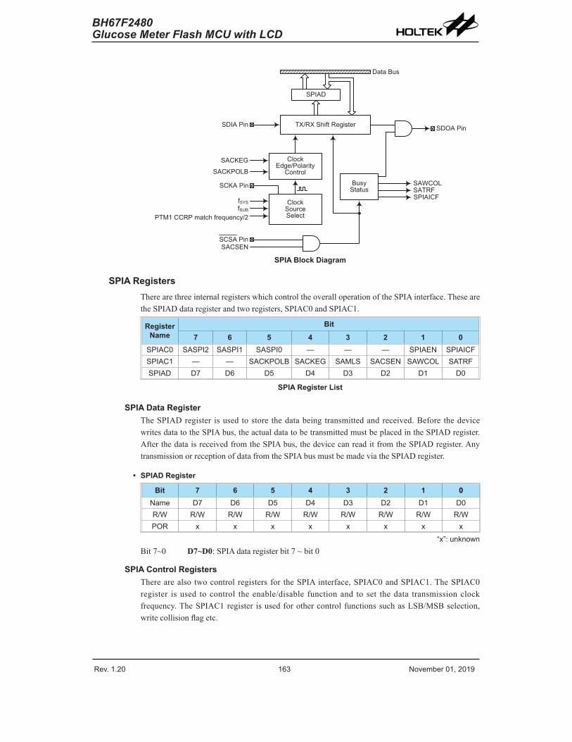
Rev. 1.20 162 November 01, 2019 Rev. 1.20 163 November 01, 2019
BH67F2480Glucose Meter Flash MCU with LCD
BH67F2480Glucose Meter Flash MCU with LCD
SPIAD
TX/RX Shift RegisterSDIA Pin
Clock Edge/Polarity
Control
SACKEG
SACKPOLB
ClockSourceSelect
fSYSfSUB
PTM1 CCRP match frequency/2
SACSEN
Busy Status
SDOA Pin
SAWCOLSATRF
SCSA Pin
Data Bus
SPIAICF
SCKA Pin
SPIA Block Diagram
SPIA RegistersThere are three internal registers which control the overall operation of the SPIA interface. These are the SPIAD data register and two registers, SPIAC0 and SPIAC1.
RegisterName
Bit7 6 5 4 3 2 1 0
SPIAC0 SASPI2 SASPI1 SASPI0 — — — SPIAEN SPIAICFSPIAC1 — — SACKPOLB SACKEG SAMLS SACSEN SAWCOL SATRFSPIAD D7 D6 D5 D4 D3 D2 D1 D0
SPIA Register List
SPIA Data RegisterThe SPIAD register is used to store the data being transmitted and received. Before the device writes data to the SPIA bus, the actual data to be transmitted must be placed in the SPIAD register. After the data is received from the SPIA bus, the device can read it from the SPIAD register. Any transmission or reception of data from the SPIA bus must be made via the SPIAD register.
• SPIAD Register
Bit 7 6 5 4 3 2 1 0Name D7 D6 D5 D4 D3 D2 D1 D0R/W R/W R/W R/W R/W R/W R/W R/W R/WPOR x x x x x x x x
“x”: unknownBit 7~0 D7~D0: SPIA data register bit 7 ~ bit 0
SPIA Control RegistersThere are also two control registers for the SPIA interface, SPIAC0 and SPIAC1. The SPIAC0 register is used to control the enable/disable function and to set the data transmission clock frequency. The SPIAC1 register is used for other control functions such as LSB/MSB selection, write collision flag etc.

Rev. 1.20 164 November 01, 2019 Rev. 1.20 165 November 01, 2019
BH67F2480Glucose Meter Flash MCU with LCD
BH67F2480Glucose Meter Flash MCU with LCD
• SPIAC0 Register
Bit 7 6 5 4 3 2 1 0Name SASPI2 SASPI1 SASPI0 — — — SPIAEN SPIAICFR/W R/W R/W R/W — — — R/W R/WPOR 1 1 1 — — — 0 0
Bit 7~5 SASPI2~SASPI0: SPIA Operating Mode Control000: SPIA master mode; SPIA clock is fSYS/4001: SPIA master mode; SPIA clock is fSYS/16010: SPIA master mode; SPIA clock is fSYS/64011: SPIA master mode; SPIA clock is fSUB
100: SPIA master mode; SPIA clock is PTM1 CCRP match frequency/2101: SPIA slave mode110: Unimplemented111: Unimplemented
These bits are used to control the SPIA Master/Slave selection and the SPIA Master clock frequency. The SPIA clock is a function of the system clock but can also be chosen to be sourced from PTM1 and fSUB. If the SPIA Slave Mode is selected then the clock will be supplied by an external Master device.
Bit 4~2 Unimplemented, read as “0”Bit 1 SPIAEN: SPIA Enable Control
0: Disable1: Enable
The bit is the overall on/off control for the SPIA interface. When the SPIAEN bit is cleared to zero to disable the SPIA interface, the SDIA, SDOA, SCKA and SCSA lines will lose their SPIA function and the SPIA operating current will be reduced to a minimum value. When the bit is high the SPIA interface is enabled.
Bit 0 SPIAICF: SPIA Incomplete Flag0: SPIA incomplete condition is not occurred1: SPIA incomplete condition is occurred
This bit is only available when the SPIA is configured to operate in an SPIA slave mode. If the SPIA operates in the slave mode with the SPIAEN and SACSEN bits both being set to 1 but the SCSA line is pulled high by the external master device before the SPIA data transfer is completely finished, the SPIAICF bit will be set to 1 together with the SATRF bit. When this condition occurs, the corresponding interrupt will occur if the interrupt function is enabled. However, the SATRF bit will not be set to 1 if the SPIAICF bit is set to 1 by software application program.
• SPIAC1 Register
Bit 7 6 5 4 3 2 1 0Name — — SACKPOLB SACKEG SAMLS SACSEN SAWCOL SATRFR/W — — R/W R/W R/W R/W R/W R/WPOR — — 0 0 0 0 0 0
Bit 7~6 Unimplemented, read as “0”.Bit 5 SACKPOLB: SPIA clock line base condition selection
0: The SCKA line will be high when the clock is inactive1: The SCKA line will be low when the clock is inactive
The SACKPOLB bit determines the base condition of the clock line, if the bit is high, then the SCKA line will be low when the clock is inactive. When the SACKPOLB bit is low, then the SCKA line will be high when the clock is inactive.

Rev. 1.20 164 November 01, 2019 Rev. 1.20 165 November 01, 2019
BH67F2480Glucose Meter Flash MCU with LCD
BH67F2480Glucose Meter Flash MCU with LCD
Bit 4 SACKEG: SPIA SCKA clock active edge type selectionSACKPOLB=0
0: SCKA has high base level with data capture on SCKA rising edge1: SCKA has high base level with data capture on SCKA falling edge
SACKPOLB=10: SCKA has low base level with data capture on SCKA falling edge1: SCKA has low base level with data capture on SCKA rising edge
The SACKEG and SACKPOLB bits are used to setup the way that the clock signal outputs and inputs data on the SPIA bus. These two bits must be configured before a data transfer is executed otherwise an erroneous clock edge may be generated. The SACKPOLB bit determines the base condition of the clock line, if the bit is high, then the SCKA line will be low when the clock is inactive. When the SACKPOLB bit is low, then the SCKA line will be high when the clock is inactive. The SACKEG bit determines active clock edge type which depends upon the condition of the SACKPOLB bit.
Bit 3 SAMLS: SPIA data shift order0: LSB first1: MSB first
This is the data shift select bit and is used to select how the data is transferred, either MSB or LSB first. Setting the bit high will select MSB first and low for LSB first.
Bit 2 SACSEN: SPIA SCSA pin control0: Disable1: Enable
The SACSEN bit is used as an enable/disable for the SCSA pin. If this bit is low, then the SCSA pin will be disabled and placed into a floating condition. If the bit is high the SCSA pin will be enabled and used as a select pin.
Bit 1 SAWCOL: SPIA write collision flag0: No collision1: Collision
The SAWCOL flag is used to detect if a data collision has occurred. If this bit is high it means that data has been attempted to be written to the SPIAD register during a data transfer operation. This writing operation will be ignored if data is being transferred. The bit can be cleared by the application program.
Bit 0 SATRF: SPIA Transmit/Receive complete flag0: SPIA data is being transferred1: SPIA data transmission is completed
The SATRF bit is the Transmit/Receive Complete flag and is set “1” automatically when an SPIA data transmission is completed, but must be cleared to zero by the application program. It can be used to generate an interrupt.
SPIA CommunicationAfter the SPIA interface is enabled by setting the SPIAEN bit high, then in the Master Mode, when data is written to the SPIAD register, transmission/reception will begin simultaneously. When the data transfer is complete, the SATRF flag will be set automatically, but must be cleared using the application program. In the Slave Mode, when the clock signal from the master has been received, any data in the SPIAD register will be transmitted and any data on the SDIA pin will be shifted into the SPIAD register. The master should output an SCSA signal to enable the slave device before a clock signal is provided. The slave data to be transferred should be well prepared at the appropriate moment relative to the SCSA signal depending upon the configurations of the SACKPOLB bit and SACKEG bit. The accompanying timing diagram shows the relationship between the slave data and SCSA signal for various configurations of the SACKPOLB and SACKEG bits.

Rev. 1.20 166 November 01, 2019 Rev. 1.20 167 November 01, 2019
BH67F2480Glucose Meter Flash MCU with LCD
BH67F2480Glucose Meter Flash MCU with LCD
The SPIA will continue to function in certain IDLE Modes if the clock source used by the SPIA interface is still active.
SCKA (SACKPOLB=1, SACKEG=0)
SCKA (SACKPOLB=0, SACKEG=0)
SCKA (SACKPOLB=1, SACKEG=1)
SCKA (SACKPOLB=0, SACKEG=1)
SCSA
SDOA (SACKEG=0)
SDOA (SACKEG=1)
SDIA Data CaptureWrite to SPIAD
SPIAEN, SACSEN=1SPIAEN=1, SACSEN=0 (External Pull-high)
D7/D0 D6/D1 D5/D2 D4/D3 D3/D4 D2/D5 D1/D6 D0/D7
D7/D0 D6/D1 D5/D2 D4/D3 D3/D4 D2/D5 D1/D6 D0/D7
SPIA Master Mode Timing
SCKA (SACKPOLB=1)
SCKA (SACKPOLB=0)
SCSA
SDOA
SDIA Data Capture
Write to SPIAD(SDOA does not change until first SCKA edge)
D7/D0 D6/D1 D5/D2 D4/D3 D3/D4 D2/D5 D1/D6 D0/D7
SPIA Slave Mode Timing – SACKEG=0
SCKA (SACKPOLB=1)
SCKA (SACKPOLB=0)
SCSA
SDOA
SDIA Data Capture
D7/D0 D6/D1 D5/D2 D4/D3 D3/D4 D2/D5 D1/D6 D0/D7
Write to SPIAD(SDOA changes as soon as writing occurs; SDOA is floating if SCSA=1)
Note: For SPIA slave mode, if SPIAEN=1 and SACSEN=0, SPIA is always enabled and ignores the SCSA level.
SPIA Slave Mode Timing – SACKEG=1

Rev. 1.20 166 November 01, 2019 Rev. 1.20 167 November 01, 2019
BH67F2480Glucose Meter Flash MCU with LCD
BH67F2480Glucose Meter Flash MCU with LCD
Clear SAWCOL Write Data into SPIAD
SAWCOL=1?
Transmission completed?(SATRF=1?)
Read Data from SPIAD
Clear SATRF
END
Transferfinished?
ASPIA Transfer
Master or Slave?
SPIAEN=1
Configure SACKPOLB, SACKEG, SACSEN and SAMLS
A
SASPI[2:0]=000, 001, 010, 011 or 100 SASPI[2:0]=101
Master Slave
Y
Y
N
N
N
Y
SPIA Transfer Control Flowchart
SPIA Bus Enable/DisableTo enable the SPIA bus, set SACSEN=1 and SCSA=0, then wait for data to be written into the SPIAD (TXRX buffer) register. For the Master Mode, after data has been written to the SPIAD (TXRX buffer) register, then transmission or reception will start automatically. When all the data has been transferred the SATRF bit should be set. For the Slave Mode, when clock pulses are received on SCKA, data in the TXRX buffer will be shifted out or data on SDIA will be shifted in.
When the SPIA bus is disabled, SCKA, SDIA, SDOA, SCSA can become I/O pins or other pin-shared functions using the corresponding pin-shared control bits.

Rev. 1.20 168 November 01, 2019 Rev. 1.20 169 November 01, 2019
BH67F2480Glucose Meter Flash MCU with LCD
BH67F2480Glucose Meter Flash MCU with LCD
SPIA Operation StepsAll communication is carried out using the 4-line interface for either Master or Slave Mode.
The SACSEN bit in the SPIAC1 register controls the overall function of the SPIA interface. Setting this bit high will enable the SPIA interface by allowing the SCSA line to be active, which can then be used to control the SPIA interface. If the SACSEN bit is low, the SPIA interface will be disabled and the SCSA line will be in a floating condition and can therefore not be used for control of the SPIA interface. If the SACSEN bit and the SPIAEN bit in the SPIAC0 register are set high, this will place the SDIA line in a floating condition and the SDOA line high. If in Master Mode the SCKA line will be either high or low depending upon the clock polarity selection bit SACKPOLB in the SPIAC1 register. If in Slave Mode the SCKA line will be in a floating condition. If SPIAEN is low then the bus will be disabled and SCSA, SDIA, SDOA and SCKA will all become I/O pins or the other functions using the corresponding pin-shared control bits. In the Master Mode the Master will always generate the clock signal. The clock and data transmission will be initiated after data has been written into the SPIAD register. In the Slave Mode, the clock signal will be received from an external master device for both data transmission and reception. The following sequences show the order to be followed for data transfer in both Master and Slave Mode.
Master Mode• Step 1
Select the clock source and Master mode using the SASPI2~SASPI0 bits in the SPIAC0 control register.
• Step 2Setup the SACSEN bit and setup the SAMLS bit to choose if the data is MSB or LSB first, this must be same as the Slave device.
• Step 3Setup the SPIAEN bit in the SPIAC0 control register to enable the SPIA interface.
• Step 4For write operations: write the data to the SPIAD register, which will actually place the data into the TXRX buffer. Then use the SCKA and SCSA lines to output the data. After this go to step 5.For read operations: the data transferred in on the SDIA line will be stored in the TXRX buffer until all the data has been received at which point it will be latched into the SPIAD register.
• Step 5Check the SAWCOL bit if set high then a collision error has occurred so return to step 4. If equal to zero then go to the following step.
• Step 6Check the SATRF bit or wait for a SPIA serial bus interrupt.
• Step 7Read data from the SPIAD register.
• Step 8Clear SATRF.
• Step 9Go to step 4.

Rev. 1.20 168 November 01, 2019 Rev. 1.20 169 November 01, 2019
BH67F2480Glucose Meter Flash MCU with LCD
BH67F2480Glucose Meter Flash MCU with LCD
Slave Mode• Step 1
Select the SPIA Slave mode using the SASPI2~SASPI0 bits in the SPIAC0 control register.
• Step 2Setup the SACSEN bit and setup the SAMLS bit to choose if the data is MSB or LSB first, this setting must be the same with the Master device.
• Step 3Setup the SPIAEN bit in the SPIAC0 control register to enable the SPIA interface.
• Step 4For write operations: write the data to the SPIAD register, which will actually place the data into the TXRX buffer. Then wait for the master clock SCKA and SCSA signal. After this, go to step 5.For read operations: the data transferred in on the SDIA line will be stored in the TXRX buffer until all the data has been received at which point it will be latched into the SPIAD register.
• Step 5Check the SAWCOL bit if set high then a collision error has occurred so return to step 4. If equal to zero then go to the following step.
• Step 6Check the SATRF bit or wait for a SPIA serial bus interrupt.
• Step 7Read data from the SPIAD register.
• Step 8Clear SATRF.
• Step 9Go to step 4.
Error DetectionThe SAWCOL bit in the SPIAC1 register is provided to indicate errors during data transfer. The bit is set by the SPIA serial Interface but must be cleared by the application program. This bit indicates a data collision has occurred which happens if a write to the SPIAD register takes place during a data transfer operation and will prevent the write operation from continuing.

Rev. 1.20 170 November 01, 2019 Rev. 1.20 171 November 01, 2019
BH67F2480Glucose Meter Flash MCU with LCD
BH67F2480Glucose Meter Flash MCU with LCD
UART Interfaces – UART0 & UART1The device contains two integrated full-duplex asynchronous serial communications UART interfaces that enable communication with external devices that contain a serial interface. Each UART function has many features and can transmit and receive data serially by transferring a frame of data with eight or nine data bits per transmission as well as being able to detect errors when the data is overwritten or incorrectly framed. Each UART function possesses its own internal interrupt which can be used to indicate when a reception occurs or when a transmission terminates.
The integrated UART functions contain the following features:
• Full-duplex, asynchronous communication
• 8 or 9 bits character length
• Even, odd or no parity options
• One or two stop bits
• Baud rate generator with 8-bit prescaler
• Parity, framing, noise and overrun error detection
• Support for interrupt on address detect (last character bit=1)
• Separately enabled transmitter and receiver
• 2-byte Deep FIFO Receive Data Buffer
• RXn pin wake-up function
• Transmit and receive interrupts
• Interrupts can be initialized by the following conditions: ♦ Transmitter Empty ♦ Transmitter Idle ♦ Receiver Full ♦ Receiver Overrun ♦ Address Mode Detect
MSB LSB…………………………
Transmitter Shift Register (TSRn)MSB LSB…………………………
Receiver Shift Register (RSRn)TXn Pin RXn Pin
Baud Rate Generator
TXR_RXRn Register TXR_RXRn Register
Data to be transmitted Data received
BufferfH
MCU Data Bus
UARTn Data Transfer Block Diagram (n=0~1)

Rev. 1.20 170 November 01, 2019 Rev. 1.20 171 November 01, 2019
BH67F2480Glucose Meter Flash MCU with LCD
BH67F2480Glucose Meter Flash MCU with LCD
UARTn External PinsTo communicate with an external serial interface, the internal UARTn has two external pins known as TXn and RXn. The TXn and RXn pins are the UART transmitter and receiver pins respectively. The TXn and RXn pin function should first be selected by the corresponding pin-shared function selection register before the UARTn function is used. Along with the UARTENn bit, the TXENn and RXENn bits, if set, will setup these pins to their respective TXn output and RXn input conditions and disable any pull-high resistor option which may exist on the TXn and RXn pins. When the TXn or RXn pin function is disabled by clearing the UARTENn, TXENn or RXENn bit, the TXn or RXn pin will be placed into a floating state. At this time whether the internal pull-high resistor is connected to the TXn or RXn pin or not is determined by the corresponding I/O pull-high function control bit.
UARTn Data Transfer SchemeThe above block diagram shows the overall data transfer structure arrangement for the UARTn. The actual data to be transmitted from the MCU is first transferred to the TXR_RXRn register by the application program. The data will then be transferred to the Transmit Shift Register from where it will be shifted out, LSB first, onto the TXn pin at a rate controlled by the Baud Rate Generator. Only the TXR_RXRn register is mapped onto the MCU Data Memory, the Transmit Shift Register is not mapped and is therefore inaccessible to the application program.
Data to be received by the UARTn is accepted on the external RXn pin, from where it is shifted in, LSB first, to the Receiver Shift Register at a rate controlled by the Baud Rate Generator. When the shift register is full, the data will then be transferred from the shift register to the internal TXR_RXRn register, where it is buffered and can be manipulated by the application program. Only the TXR_RXRn register is mapped onto the MCU Data Memory, the Receiver Shift Register is not mapped and is therefore inaccessible to the application program.
It should be noted that the actual register for data transmission and reception only exists as a single shared register in the Data Memory. This shared register known as the TXR_RXRn register is used for both data transmission and data reception.
UARTn Status and Control RegistersThere are five control registers associated with the UARTn function. The UnSR, UnCR1 and UnCR2 registers control the overall function of the UARTn, while the BRGn register controls the Baud rate. The actual data to be transmitted and received on the serial interface is managed through the TXR_RXRn data register.
RegisterName
Bit7 6 5 4 3 2 1 0
UnSR PERRn NFn FERRn OERRn RIDLEn RXIFn TIDLEn TXIFnUnCR1 UARTENn BNOn PRENn PRTn STOPSn TXBRKn RX8n TX8nUnCR2 TXENn RXENn BRGHn ADDENn WAKEn RIEn TIIEn TEIEn
TXR_RXRn TXRXn7 TXRXn6 TXRXn5 TXRXn4 TXRXn3 TXRXn2 TXRXn1 TXRXn0BRGn BRGn7 BRGn6 BRGn5 BRGn4 BRGn3 BRGn2 BRGn1 BRGn0
UARTn Register List (n=0~1)

Rev. 1.20 172 November 01, 2019 Rev. 1.20 173 November 01, 2019
BH67F2480Glucose Meter Flash MCU with LCD
BH67F2480Glucose Meter Flash MCU with LCD
UnSR RegisterThe UnSR register is the status register for the UARTn, which can be read by the program to determine the present status of the UARTn. All flags within the UnSR register are read only. Further explanation on each of the flags is given below:
Bit 7 6 5 4 3 2 1 0Name PERRn NFn FERRn OERRn RIDLEn RXIFn TIDLEn TXIFnR/W R R R R R R R RPOR 0 0 0 0 1 0 1 1
Bit 7 PERRn: Parity error flag0: No parity error is detected1: Parity error is detected
The PERRn flag is the parity error flag. When this read only flag is “0”, it indicates a parity error has not been detected. When the flag is “1”, it indicates that the parity of the received word is incorrect. This error flag is applicable only if Parity mode (odd or even) is selected. The flag can also be cleared by a software sequence which involves a read to the status register UnSR followed by an access to the TXR_RXRn data register.
Bit 6 NFn: Noise flag0: No noise is detected1: Noise is detected
The NFn flag is the noise flag. When this read only flag is “0”, it indicates no noise condition. When the flag is “1”, it indicates that the UARTn has detected noise on the receiver input. The NFn flag is set during the same cycle as the RXIFn flag but will not be set in the case of as overrun. The NFn flag can be cleared by a software sequence which will involve a read to the status register UnSR followed by an access to the TXR_RXRn data register.
Bit 5 FERRn: Framing error flag0: No framing error is detected1: Framing error is detected
The FERRn flag is the framing error flag. When this read only flag is “0”, it indicates that there is no framing error. When the flag is “1”, it indicates that a framing error has been detected for the current character. The flag can also be cleared by a software sequence which will involve a read to the status register UnSR followed by an access to the TXR_RXRn data register.
Bit 4 OERRn: Overrun error flag0: No overrun error is detected1: Overrun error is detected
The OERRn flag is the overrun error flag which indicates when the receiver buffer has overflowed. When this read only flag is “0”, it indicates that there is no overrun error. When the flag is “1”, it indicates that an overrun error occurs which will inhibit further transfers to the TXR_RXRn receive data register. The flag is cleared by a software sequence, which is a read to the status register UnSR followed by an access to the TXR_RXRn data register.
Bit 3 RIDLEn: Receiver status0: Data reception is in progress (Data being received)1: No data reception is in progress (Receiver is idle)
The RIDLEn flag is the receiver status flag. When this read only flag is “0”, it indicates that the receiver is between the initial detection of the start bit and the completion of the stop bit. When the flag is “1”, it indicates that the receiver is idle. Between the completion of the stop bit and the detection of the next start bit, the RIDLEn bit is “1” indicating that the UARTn receiver is idle and the RXn pin stays in logic high condition.

Rev. 1.20 172 November 01, 2019 Rev. 1.20 173 November 01, 2019
BH67F2480Glucose Meter Flash MCU with LCD
BH67F2480Glucose Meter Flash MCU with LCD
Bit 2 RXIFn: Receive TXR_RXRn data register status0: TXR_RXRn data register is empty1: TXR_RXRn data register has available data
The RXIFn flag is the receive data register status flag. When this read only flag is “0”, it indicates that the TXR_RXRn read data register is empty. When the flag is “1”, it indicates that the TXR_RXRn read data register contains new data. When the contents of the shift register are transferred to the TXR_RXRn register, an interrupt is generated if RIEn=1 in the UnCR2 register. If one or more errors are detected in the received word, the appropriate receive-related flags NFn, FERRn, and/or PERRn are set within the same clock cycle. The RXIFn flag will eventually be cleared when the UnSR register is read with RXIFn set, followed by a read from the TXR_RXR register, and if the TXR_RXR register has no more new data available.
Bit 1 TIDLEn: Transmission idle0: Data transmission is in progress (Data being transmitted)1: No data transmission is in progress (Transmitter is idle)
The TIDLEn flag is known as the transmission complete flag. When this read only flag is “0”, it indicates that a transmission is in progress. This flag will be set high when the TXIFn flag is “1” and when there is no transmit data or break character being transmitted. When TIDLEn is equal to “1”, the TXn pin becomes idle with the pin state in logic high condition. The TIDLEn flag is cleared by reading the UnSR register with TIDLEn set and then writing to the TXR_RXRn register. The flag is not generated when a data character or a break is queued and ready to be sent.
Bit 0 TXIFn: Transmit TXR_RXRn data register status0: Character is not transferred to the transmit shift register1: Character has transferred to the transmit shift register (TXR_RXRn data register
is empty)The TXIFn flag is the transmit data register empty flag. When this read only flag is “0”, it indicates that the character is not transferred to the transmitter shift register. When the flag is “1”, it indicates that the transmitter shift register has received a character from the TXR_RXRn data register. The TXIFn flag is cleared by reading the UARTn status register (UnSR) with TXIFn set and then writing to the TXR_RXRn data register. Note that when the TXENn bit is set, the TXIFn flag bit will also be set since the transmit data register is not yet full.
UnCR1 RegisterThe UnCR1 register together with the UnCR2 register are the two UARTn control registers that are used to set the various options for the UARTn function, such as overall on/off control, parity control, data transfer bit length etc. Further explanation on each of the bits is given below:
Bit 7 6 5 4 3 2 1 0Name UARTENn BNOn PRENn PRTn STOPSn TXBRKn RX8n TX8nR/W R/W R/W R/W R/W R/W R/W R WPOR 0 0 0 0 0 0 x 0
“x”: unknownBit 7 UARTENn: UARTn function enable control
0: Disable UARTn. TXn and RXn pins are in a floating state1: Enable UARTn. TXn and RXn pins function as UARTn pins
The UARTENn bit is the UARTn enable bit. When this bit is equal to “0”, the UARTn will be disabled and the RXn pin as well as the TXn pin will be in a floating state. When the bit is equal to “1”, the UARTn will be enabled and the TXn and RXn pins will function as defined by the TXENn and RXENn enable control bits.When the UARTn is disabled, it will empty the buffer so any character remaining in the buffer will be discarded. In addition, the value of the baud rate counter will be reset. If the UARTn is disabled, all error and status flags will be reset. Also the TXENn, RXENn, TXBRKn, RXIFn, OERRn, FERRn, PERRn and NFn bits will be

Rev. 1.20 174 November 01, 2019 Rev. 1.20 175 November 01, 2019
BH67F2480Glucose Meter Flash MCU with LCD
BH67F2480Glucose Meter Flash MCU with LCD
cleared, while the TIDLEn, TXIFn and RIDLEn bits will be set. Other control bits in UnCR1, UnCR2 and BRGn registers will remain unaffected. If the UARTn is active and the UARTENn bit is cleared, all pending transmissions and receptions will be terminated and the module will be reset as defined above. When the UARTn is re-enabled, it will restart in the same configuration.
Bit 6 BNOn: Number of data transfer bits selection0: 8-bit data transfer1: 9-bit data transfer
This bit is used to select the data length format, which can have a choice of either 8-bit or 9-bit format. When this bit is equal to “1”, a 9-bit data length format will be selected. If the bit is equal to “0”, then an 8-bit data length format will be selected. If 9-bit data length format is selected, then bits RX8n and TX8n will be used to store the 9th bit of the received and transmitted data respectively.
Bit 5 PRENn: Parity function enable control0: Parity function is disabled1: Parity function is enabled
This is the parity enable bit. When this bit is equal to “1", the parity function will be enabled. If the bit is equal to “0”, then the parity function will be disabled.
Bit 4 PRTn: Parity type selection bit0: Even parity for parity generator1: Odd parity for parity generator
This bit is the parity type selection bit. When this bit is equal to “1”, odd parity type will be selected. If the bit is equal to “0”, then even parity type will be selected.
Bit 3 STOPSn: Number of Stop bits selection0: One stop bit format is used1: Two stop bits format is used
This bit determines if one or two stop bits are to be used. When this bit is equal to “1”, two stop bits are used. If this bit is equal to “0”, then only one stop bit is used.
Bit 2 TXBRKn: Transmit break character0: No break character is transmitted1: Break characters transmit
The TXBRKn bit is the Transmit Break Character bit. When this bit is “0”, there are no break characters and the TXn pin operates normally. When the bit is “1”, there are transmit break characters and the transmitter will send logic zeros. When this bit is equal to “1”, after the buffered data has been transmitted, the transmitter output is held low for a minimum of a 13-bit length and until the TXBRKn bit is reset.
Bit 1 RX8n: Receive data bit 8 for 9-bit data transfer format (read only)This bit is only used if 9-bit data transfers are used, in which case this bit location will store the 9th bit of the received data known as RX8n. The BNOn bit is used to determine whether data transfers are in 8-bit or 9-bit format.
Bit 0 TX8n: Transmit data bit 8 for 9-bit data transfer format (write only)This bit is only used if 9-bit data transfers are used, in which case this bit location will store the 9th bit of the transmitted data known as TX8n. The BNOn bit is used to determine whether data transfers are in 8-bit or 9-bit format.

Rev. 1.20 174 November 01, 2019 Rev. 1.20 175 November 01, 2019
BH67F2480Glucose Meter Flash MCU with LCD
BH67F2480Glucose Meter Flash MCU with LCD
UnCR2 RegisterThe UnCR2 register is the second of the two UARTn control registers and serves several purposes. One of its main functions is to control the basic enable/disable operation of the UARTn Transmitter and Receiver as well as enabling the various UARTn interrupt sources. The register also serves to control the baud rate speed, receiver wake-up enable and the address detect enable. Further explanation on each of the bits is given below:
Bit 7 6 5 4 3 2 1 0Name TXENn RXENn BRGHn ADDENn WAKEn RIEn TIIEn TEIEnR/W R/W R/W R/W R/W R/W R/W R/W R/WPOR 0 0 0 0 0 0 0 0
Bit 7 TXENn: UARTn Transmitter enabled control0: UARTn transmitter is disabled1: UARTn transmitter is enabled
The bit named TXENn is the Transmitter Enable Bit. When this bit is equal to “0”, the transmitter will be disabled with any pending data transmissions being aborted. In addition the buffers will be reset. In this situation the TXn pin will be in a floating state. If the TXENn bit is equal to “1” and the UARTENn bit is also equal to “1”, the transmitter will be enabled and the TXn pin will be controlled by the UARTn. Clearing the TXENn bit during a transmission will cause the data transmission to be aborted and will reset the transmitter. If this situation occurs, the TXn pin will be in a floating state.
Bit 6 RXENn: UARTn Receiver enabled control0: UARTn receiver is disabled1: UARTn receiver is enabled
The bit named RXENn is the Receiver Enable Bit. When this bit is equal to “0”, the receiver will be disabled with any pending data receptions being aborted. In addition the receive buffers will be reset. In this situation the RXn pin will be in a floating state. If the RXENn bit is equal to “1” and the UARTENn bit is also equal to “1”, the receiver will be enabled and the RXn pin will be controlled by the UARTn. Clearing the RXENn bit during a reception will cause the data reception to be aborted and will reset the receiver. If this situation occurs, the RXn pin will be in a floating state.
Bit 5 BRGHn: Baud Rate speed selection0: Low speed baud rate1: High speed baud rate
The bit named BRGHn selects the high or low speed mode of the Baud Rate Generator. This bit, together with the value placed in the baud rate register BRGn, controls the Baud Rate of the UARTn. If this bit is equal to “1”, the high speed mode is selected. If the bit is equal to “0”, the low speed mode is selected.
Bit 4 ADDENn: Address detect function enable control0: Address detect function is disabled1: Address detect function is enabled
The bit named ADDENn is the address detect function enable control bit. When this bit is equal to “1”, the address detect function is enabled. When it occurs, if the 8th bit, which corresponds to RX7n if BNOn=0 or the 9th bit, which corresponds to RX8n if BNOn=1, has a value of “1”, then the received word will be identified as an address, rather than data. If the corresponding interrupt is enabled, an interrupt request will be generated each time the received word has the address bit set, which is the 8th or 9th bit depending on the value of BNOn. If the address bit known as the 8th or 9th bit of the received word is “0” with the address detect function being enabled, an interrupt will not be generated and the received data will be discarded.

Rev. 1.20 176 November 01, 2019 Rev. 1.20 177 November 01, 2019
BH67F2480Glucose Meter Flash MCU with LCD
BH67F2480Glucose Meter Flash MCU with LCD
Bit 3 WAKEn: RXn pin wake-up UARTn function enable control0: RXn pin wake-up UARTn function is disabled1: RXn pin wake-up UARTn function is enabled
This bit is used to control the wake-up UARTn function when a falling edge on the RXn pin occurs. Note that this bit is only available when the UARTn clock (fH) is switched off. There will be no RXn pin wake-up UARTn function if the UARTn clock (fH) exists. If the WAKEn bit is set to 1 as the UARTn clock (fH) is switched off, a UARTn wake-up request will be initiated when a falling edge on the RXn pin occurs. When this request happens and the corresponding interrupt is enabled, an RXn pin wake-up UARTn interrupt will be generated to inform the MCU to wake up the UARTn function by switching on the UARTn clock (fH) via the application program. Otherwise, the UARTn function can not resume even if there is a falling edge on the RXn pin when the WAKEn bit is cleared to 0.
Bit 2 RIEn: Receiver interrupt enable control0: Receiver related interrupt is disabled1: Receiver related interrupt is enabled
This bit enables or disables the receiver interrupt. If this bit is equal to “1” and when the receiver overrun flag OERRn or receive data available flag RXIFn is set, the UARTn interrupt request flag will be set. If this bit is equal to “0”, the UARTn interrupt request flag will not be influenced by the condition of the OERRn or RXIFn flags.
Bit 1 TIIEn: Transmitter Idle interrupt enable control0: Transmitter idle interrupt is disabled1: Transmitter idle interrupt is enabled
This bit enables or disables the transmitter idle interrupt. If this bit is equal to “1” and when the transmitter idle flag TIDLEn is set, due to a transmitter idle condition, the UARTn interrupt request flag will be set. If this bit is equal to “0”, the UARTn interrupt request flag will not be influenced by the condition of the TIDLEn flag.
Bit 0 TEIEn: Transmitter Empty interrupt enable control0: Transmitter empty interrupt is disabled1: Transmitter empty interrupt is enabled
This bit enables or disables the transmitter empty interrupt. If this bit is equal to “1” and when the transmitter empty flag TXIFn is set, due to a transmitter empty condition, the UARTn interrupt request flag will be set. If this bit is equal to “0”, the UARTn interrupt request flag will not be influenced by the condition of the TXIFn flag.
TXR_RXRn RegisterBit 7 6 5 4 3 2 1 0
Name TXRXn7 TXRXn6 TXRXn5 TXRXn4 TXRXn3 TXRXn2 TXRXn1 TXRXn0R/W R/W R/W R/W R/W R/W R/W R/W R/WPOR x x x x x x x x
“x”: unknownBit 7~0 TXRXn7~TXRXn0: UARTn Transmit/Receive Data bit 7 ~ bit 0
• BRGn Register
Bit 7 6 5 4 3 2 1 0Name BRGn7 BRGn6 BRGn5 BRGn4 BRGn3 BRGn2 BRGn1 BRGn0R/W R/W R/W R/W R/W R/W R/W R/W R/WPOR x x x x x x x x
“x”: unknownBit 7~0 BRGn7~ BRGn0: Baud Rate values
By programming the BRGHn bit in UnCR2 Register which allows selection of the related formula described above and programming the required value in the BRGn register, the required baud rate can be setup.Note: Baud rate= fH / [64 × (N+1)] if BRGHn=0. Baud rate= fH / [16 × (N+1)] if BRGHn=1.

Rev. 1.20 176 November 01, 2019 Rev. 1.20 177 November 01, 2019
BH67F2480Glucose Meter Flash MCU with LCD
BH67F2480Glucose Meter Flash MCU with LCD
Baud Rate GeneratorTo setup the speed of the serial data communication, the UARTn function contains its own dedicated baud rate generator. The baud rate is controlled by its own internal free running 8-bit timer, the period of which is determined by two factors. The first of these is the value placed in the baud rate register BRGn and the second is the value of the BRGHn bit with the control register UnCR2. The BRGHn bit decides if the baud rate generator is to be used in a high speed mode or low speed mode, which in turn determines the formula that is used to calculate the baud rate. The value N in the BRGn register which is used in the following baud rate calculation formula determines the division factor. Note that N is the decimal value placed in the BRGn register and has a range of between 0 and 255.
UnCR2 BRGHn Bit 0 1Baud Rate (BR) fH / [64 (N+1)] fH / [16 (N+1)]
By programming the BRGHn bit which allows selection of the related formula and programming the required value in the BRGn register, the required baud rate can be setup. Note that because the actual baud rate is determined using a discrete value, N, placed in the BRGn register, there will be an error associated between the actual and requested value. The following example shows how the BRGn register value N and the error value can be calculated.
Calculating the Baud Rate and Error ValuesFor a clock frequency of 4MHz, and with BRGHn cleared to zero determine the BRGn register value N, the actual baud rate and the error value for a desired baud rate of 4800.
From the above table the desired baud rate BR = fH / [64 (N+1)]
Re-arranging this equation gives N = [fH / (BR×64)] - 1
Giving a value for N = [4000000 / (4800×64)] - 1 = 12.0208
To obtain the closest value, a decimal value of 12 should be placed into the BRGn register. This gives an actual or calculated baud rate value of BR = 4000000 / [64 × (12+1)] = 4808
Therefore the error is equal to (4808 - 4800) / 4800 = 0.16%
UARTn Setup and ControlFor data transfer, the UARTn function utilizes a non-return-to-zero, more commonly known as NRZ, format. This is composed of one start bit, eight or nine data bits, and one or two stop bits. Parity is supported by the UARTn hardware, and can be setup to be even, odd or no parity. For the most common data format, 8 data bits along with no parity and one stop bit, denoted as 8, N, 1, is used as the default setting, which is the setting at power-on. The number of data bits and stop bits, along with the parity, are setup by programming the corresponding BNOn, PRTn, PRENn, and STOPSn bits in the UnCR1 register. The baud rate used to transmit and receive data is setup using the internal 8-bit baud rate generator, while the data is transmitted and received LSB first. Although the UARTn transmitter and receiver are functionally independent, they both use the same data format and baud rate. In all cases stop bits will be used for data transmission.
Enabling/Disabling the UARTn InterfaceThe basic on/off function of the internal UARTn function is controlled using the UARTENn bit in the UnCR1 register. If the UARTENn, TXENn and RXENn bits are set, then these two UARTn pins will act as normal TXn output pin and RXn input pin respectively. If no data is being transmitted on the TXn pin, then it will default to a logic high value.
Clearing the UARTENn bit will disable the TXn and RXn pins and allow these two pins to be used as normal I/O or other pin-shared functional pins by configuring the corresponding pin-shared

Rev. 1.20 178 November 01, 2019 Rev. 1.20 179 November 01, 2019
BH67F2480Glucose Meter Flash MCU with LCD
BH67F2480Glucose Meter Flash MCU with LCD
control bits. When the UARTn function is disabled the buffer will be reset to an empty condition, at the same time discarding any remaining residual data. Disabling the UARTn will also reset the error and status flags with bits TXENn, RXENn, TXBRKn, RXIFn, OERRn, FERRn, PERRn and NFn being cleared while bits TIDLEn, TXIFn and RIDLEn will be set. The remaining control bits in the UnCR1, UnCR2 and BRGn registers will remain unaffected. If the UARTENn bit in the UnCR1 register is cleared while the UARTn is active, then all pending transmissions and receptions will be immediately suspended and the UARTn will be reset to a condition as defined above. If the UARTn is then subsequently re-enabled, it will restart again in the same configuration.
Data, Parity and Stop Bit SelectionThe format of the data to be transferred is composed of various factors such as data bit length, parity on/off, parity type, address bits and the number of stop bits. These factors are determined by the setup of various bits within the UnCR1 register. The BNOn bit controls the number of data bits which can be set to either 8 or 9, the PRTn bit controls the choice of odd or even parity, the PRENn bit controls the parity on/off function and the STOPSn bit decides whether one or two stop bits are to be used. The following table shows various formats for data transmission. The address bit, which is the MSB of the data byte, identifies the frame as an address character or data if the address detect function is enabled. The number of stop bits, which can be either one or two, is independent of the data length and is only used for the transmitter. There is only one stop bit for the receiver.
Start Bit Data Bits Address Bit Parity Bit Stop BitExample of 8-bit Data Formats
1 8 0 0 11 7 0 1 11 7 1 0 1
Example of 9-bit Data Formats1 9 0 0 11 8 0 1 11 8 1 0 1
Transmitter Receiver Data Format
The following diagram shows the transmit and receive waveforms for both 8-bit and 9-bit data formats.
Bit 0
8-bit Data Format
Bit 1 StopBit
Next StartBit
StartBit
Parity Bit
Bit 2 Bit 3 Bit 4 Bit 5 Bit 6 Bit 7
Bit 0
9-bit Data Format
Bit 1StartBit Bit 2 Bit 3 Bit 4 Bit 5 Bit 6 Stop
Bit
Next StartBit
Parity Bit
Bit 8Bit 7
UARTn TransmitterData word lengths of either 8 or 9 bits can be selected by programming the BNOn bit in the UnCR1 register. When BNOn bit is set, the word length will be set to 9 bits. In this case the 9th bit, which is the MSB, needs to be stored in the TX8n bit in the UnCR1 register. At the transmitter core lies the Transmitter Shift Register, more commonly known as the TSRn, whose data is obtained from the transmit data register, which is known as the TXR_RXRn register. The data to be transmitted is loaded into this TXR_RXRn register by the application program. The TSRn register is not written to with new data until the stop bit from the previous transmission has been sent out. As soon as this stop bit has been transmitted, the TSRn can then be loaded with new data from the TXR_RXRn

Rev. 1.20 178 November 01, 2019 Rev. 1.20 179 November 01, 2019
BH67F2480Glucose Meter Flash MCU with LCD
BH67F2480Glucose Meter Flash MCU with LCD
register, if it is available. It should be noted that the TSRn register, unlike many other registers, is not directly mapped into the Data Memory area and as such is not available to the application program for direct read/write operations. An actual transmission of data will normally be enabled when the TXENn bit is set, but the data will not be transmitted until the TXR_RXRn register has been loaded with data and the baud rate generator has defined a shift clock source. However, the transmission can also be initiated by first loading data into the TXR_RXRn register, after which the TXENn bit can be set. When a transmission of data begins, the TSRn is normally empty, in which case a transfer to the TXR_RXRn register will result in an immediate transfer to the TSRn. If during a transmission the TXENn bit is cleared, the transmission will immediately cease and the transmitter will be reset. The TXn output pin can then be configured as the I/O or other pin-shared function by configuring the corresponding pin-shared control bits.
Transmitting DataWhen the UARTn is transmitting data, the data is shifted on the TXn pin from the shift register, with the least significant bit first. In the transmit mode, the TXR_RXRn register forms a buffer between the internal bus and the transmitter shift register. It should be noted that if 9-bit data format has been selected, then the MSB will be taken from the TX8n bit in the UnCR1 register. The steps to initiate a data transfer can be summarized as follows:
• Make the correct selection of the BNOn, PRTn, PRENn and STOPSn bits to define the required word length, parity type and number of stop bits.
• Setup the BRGn register to select the desired baud rate.
• Set the TXENn bit to ensure that the TXn pin is used as a UARTn transmitter pin.
• Access the UnSR register and write the data that is to be transmitted into the TXR_RXRn register. Note that this step will clear the TXIFn bit.
This sequence of events can now be repeated to send additional data.
It should be noted that when TXIFn=0, data will be inhibited from being written to the TXR_RXRn register. Clearing the TXIFn flag is always achieved using the following software sequence:
1. A UnSR register access
2. A TXR_RXRn register write execution
The read-only TXIFn flag is set by the UARTn hardware and if set indicates that the TXR_RXRn register is empty and that other data can now be written into the TXR_RXRn register without overwriting the previous data. If the TEIEn bit is set then the TXIFn flag will generate an interrupt.
During a data transmission, a write instruction to the TXR_RXRn register will place the data into the TXR_RXRn register, which will be copied to the shift register at the end of the present transmission. When there is no data transmission in progress, a write instruction to the TXR_RXRn register will place the data directly into the shift register, resulting in the commencement of data transmission, and the TXIFn bit being immediately set. When a frame transmission is complete, which happens after stop bits are sent or after the break frame, the TIDLEn bit will be set. To clear the TIDLEn bit the following software sequence is used:
1. A UnSR register access
2. A TXR_RXRn register write execution
Note that both the TXIFn and TIDLEn bits are cleared by the same software sequence.

Rev. 1.20 180 November 01, 2019 Rev. 1.20 181 November 01, 2019
BH67F2480Glucose Meter Flash MCU with LCD
BH67F2480Glucose Meter Flash MCU with LCD
Transmit BreakIf the TXBRKn bit is set then break characters will be sent on the next transmission. Break character transmission consists of a start bit, followed by 13×N ‘0’ bits and stop bits, where N=1, 2, etc. If a break character is to be transmitted then the TXBRKn bit must be first set by the application program, and then cleared to generate the stop bits. Transmitting a break character will not generate a transmit interrupt. Note that a break condition length is at least 13 bits long. If the TXBRKn bit is continually kept at a logic high level then the transmitter circuitry will transmit continuous break characters. After the application program has cleared the TXBRKn bit, the transmitter will finish transmitting the last break character and subsequently send out one or two stop bits. The automatic logic highs at the end of the last break character will ensure that the start bit of the next frame is recognized.
UARTn ReceiverThe UARTn is capable of receiving word lengths of either 8 or 9 bits. If the BNOn bit is set, the word length will be set to 9 bits with the MSB being stored in the RX8n bit of the UnCR1 register. At the receiver core lies the Receive Serial Shift Register, commonly known as the RSRn. The data which is received on the RXn external input pin is sent to the data recovery block. The data recovery block operating speed is 16 times that of the baud rate, while the main receive serial shifter operates at the baud rate. After the RXn pin is sampled for the stop bit, the received data in RSRn is transferred to the receive data register, if the register is empty. The data which is received on the external RXn input pin is sampled three times by a majority detect circuit to determine the logic level that has been placed onto the RXn pin. It should be noted that the RSRn register, unlike many other registers, is not directly mapped into the Data Memory area and as such is not available to the application program for direct read/write operations.
Receiving DataWhen the UARTn receiver is receiving data, the data is serially shifted in on the external RXn input pin, LSB first. In the read mode, the TXR_RXRn register forms a buffer between the internal bus and the receiver shift register. The TXR_RXRn register is a two byte deep FIFO data buffer, where two bytes can be held in the FIFO while a third byte can continue to be received. Note that the application program must ensure that the data is read from TXR_RXRn before the third byte has been completely shifted in, otherwise this third byte will be discarded and an overrun error OERRn will be subsequently indicated. The steps to initiate a data transfer can be summarized as follows:
• Make the correct selection of BNOn, PRTn and PRENn bits to define the word length, parity type.
• Setup the BRGn register to select the desired baud rate.
• Set the RXENn bit to ensure that the RXn pin is used as a UARTn receiver pin.
At this point the receiver will be enabled which will begin to look for a start bit.
When a character is received the following sequence of events will occur:
• The RXIFn bit in the UnSR register will be set when the TXR_RXRn register has data available. There will be at most one more character available before an overrun error occurs.
• When the contents of the shift register have been transferred to the TXR_RXRn register, then if the RIEn bit is set, an interrupt will be generated.
• If during reception, a frame error, noise error, parity error, or an overrun error has been detected, then the error flags can be set.
The RXIFn bit can be cleared using the following software sequence:
1. A UnSR register access
2. A TXR_RXRn register read execution

Rev. 1.20 180 November 01, 2019 Rev. 1.20 181 November 01, 2019
BH67F2480Glucose Meter Flash MCU with LCD
BH67F2480Glucose Meter Flash MCU with LCD
Receive BreakAny break character received by the UARTn will be managed as a framing error. The receiver will count and expect a certain number of bit times as specified by the values programmed into the BNOn bit plus one stop bit. If the break is much longer than 13 bit times, the reception will be considered as complete after the number of bit times specified by BNOn plus one stop bit. The RXIFn bit is set, FERRn is set, zeros are loaded into the receive data register, interrupts are generated if appropriate and the RIDLEn bit is set. A break is regarded as a character that contains only zeros with the FERRn flag set. If a long break signal has been detected, the receiver will regard it as a data frame including a start bit, data bits and the invalid stop bit and the FERRn flag will be set. The receiver must wait for a valid stop bit before looking for the next start bit. The receiver will not make the assumption that the break condition on the line is the next start bit. The break character will be loaded into the buffer and no further data will be received until stop bits are received. It should be noted that the RIDLEn read only flag will go high when the stop bits have not yet been received. The reception of a break character on the UARTn registers will result in the following:
• The framing error flag, FERRn, will be set.
• The receive data register, TXR_RXRn, will be cleared.
• The OERRn, NFn, PERRn, RIDLEn or RXIFn flags will possibly be set.
Idle StatusWhen the receiver is reading data, which means it will be in between the detection of a start bit and the reading of a stop bit, the receiver status flag in the UnSR register, otherwise known as the RIDLEn flag, will have a zero value. In between the reception of a stop bit and the detection of the next start bit, the RIDLEn flag will have a high value, which indicates the receiver is in an idle condition.
Receiver InterruptThe read only receive interrupt flag RXIFn in the UnSR register is set by an edge generated by the receiver. An interrupt is generated if RIEn=1, when a word is transferred from the Receive Shift Register, RSRn, to the Receive Data Register, TXR_RXRn. An overrun error can also generate an interrupt if RIEn=1.
Managing Receiver ErrorsSeveral types of reception errors can occur within the UARTn module, the following section describes the various types and how they are managed by the UARTn.
Overrun Error – OERRnThe TXR_RXRn register is composed of a two byte deep FIFO data buffer, where two bytes can be held in the FIFO register, while a third byte can continue to be received. Before this third byte has been entirely shifted in, the data should be read from the TXR_RXRn register. If this is not done, the overrun error flag OERRn will be consequently indicated.
In the event of an overrun error occurring, the following will happen:
• The OERRn flag in the UnSR register will be set.
• The TXR_RXRn contents will not be lost.
• The shift register will be overwritten.
• An interrupt will be generated if the RIEn bit is set.
The OERRn flag can be cleared by an access to the UnSR register followed by a read to the TXR_RXRn register.

Rev. 1.20 182 November 01, 2019 Rev. 1.20 183 November 01, 2019
BH67F2480Glucose Meter Flash MCU with LCD
BH67F2480Glucose Meter Flash MCU with LCD
Noise Error – NFnOver-sampling is used for data recovery to identify valid incoming data and noise. If noise is detected within a frame the following will occur:
• The read only noise flag, NFn, in the UnSR register will be set on the rising edge of the RXIFn bit.
• Data will be transferred from the Shift register to the TXR_RXRn register.
• No interrupt will be generated. However this bit rises at the same time as the RXIFn bit which itself generates an interrupt.
Note that the NFn flag is reset by an UnSR register read operation followed by a TXR_RXRn register read operation.
Framing Error – FERRnThe read only framing error flag, FERRn, in the UnSR register, is set if a zero is detected instead of stop bits. If two stop bits are selected, both stop bits must be high; otherwise the FERRn flag will be set. The FERRn flag and the received data will be recorded in the UnSR and TXR_RXRn registers respectively, and the flag is cleared in any reset.
Parity Error – PERRnThe read only parity error flag, PERRn, in the UnSR register, is set if the parity of the received word is incorrect. This error flag is only applicable if the parity is enabled, PRENn = 1, and if the parity type, odd or even is selected. The read only PERRn flag and the received data will be recorded in the UnSR and TXR_RXRn registers respectively. It is cleared on any reset, it should be noted that the flags, FERRn and PERRn, in the UnSR register should first be read by the application program before reading the data word.
UARTn Interrupt StructureSeveral individual UARTn conditions can generate a UARTn interrupt. When these conditions exist, a low pulse will be generated to get the attention of the microcontroller. These conditions are a transmitter data register empty, transmitter idle, receiver data available, receiver overrun, address detect and an RXn pin wake-up. When any of these conditions are created, if the global interrupt enable bit and its corresponding interrupt control bit are enabled and the stack is not full, the program will jump to its corresponding interrupt vector where it can be serviced before returning to the main program. Four of these conditions have the corresponding UnSR register flags which will generate a UARTn interrupt if its associated interrupt enable control bit in the UnCR2 register is set. The two transmitter interrupt conditions have their own corresponding enable control bits, while the two receiver interrupt conditions have a shared enable control bit. These enable bits can be used to mask out individual UARTn interrupt sources.
The address detect condition, which is also a UARTn interrupt source, does not have an associated flag, but will generate a UARTn interrupt when an address detect condition occurs if its function is enabled by setting the ADDENn bit in the UnCR2 register. An RXn pin wake-up, which is also a UARTn interrupt source, does not have an associated flag, but will generate a UARTn interrupt if the UARTn clock (fH) source is switched off and the WAKEn and RIEn bits in the UnCR2 register are set when a falling edge on the RXn pin occurs.
Note that the UnSR register flags are read only and cannot be cleared or set by the application program, neither will they be cleared when the program jumps to the corresponding interrupt servicing routine, as is the case for some of the other interrupts. The flags will be cleared automatically when certain actions are taken by the UARTn, the details of which are given in the UARTn register section. The overall UARTn interrupt can be disabled or enabled by the related interrupt enable control bits in the interrupt control registers of the microcontroller to decide whether the interrupt requested by the UARTn module is masked out or allowed.

Rev. 1.20 182 November 01, 2019 Rev. 1.20 183 November 01, 2019
BH67F2480Glucose Meter Flash MCU with LCD
BH67F2480Glucose Meter Flash MCU with LCD
Transmitter EmptyFlag TXIFn
UnSR Register
Transmitter IdleFlag TIDLEn
Receiver OverrunFlag OERRn
Receiver DataAvailable RXIFn
ADDENn
RXn PinWake-up
WAKEn 01
0
1
RX7n if BNOn=0RX8n if BNOn=1
UnCR2 Register
RIEn 01
TIIEn 01
TEIEn 01
UARTnInterrupt
Request Flag URnF
UnCR2 Register
URnE EMI
01
Interrupt signal to MCU
UARTn Interrupt Structure (n=0~1)
Address Detect ModeSetting the Address Detect Mode bit, ADDENn, in the UnCR2 register, enables this special mode. If this bit is enabled then an additional qualifier will be placed on the generation of a Receiver Data Available interrupt, which is requested by the RXIFn flag. If the ADDENn bit is enabled, then when data is available, an interrupt will only be generated, if the highest received bit has a high value. Note that the URnE and EMI interrupt enable bits must also be enabled for correct interrupt generation. This highest address bit is the 9th bit if BNOn=1 or the 8th bit if BNOn=0. If this bit is high, then the received word will be defined as an address rather than data. A Data Available interrupt will be generated every time the last bit of the received word is set. If the ADDENn bit is not enabled, then a Receiver Data Available interrupt will be generated each time the RXIFn flag is set, irrespective of the data last bit status. The address detect mode and parity enable are mutually exclusive functions. Therefore if the address detect mode is enabled, then to ensure correct operation, the parity function should be disabled by resetting the parity enable bit PRENn to zero.
ADDENn Bit 9 if BNOn=1,Bit 8 if BNOn=0
UARTn InterruptGenerated
00 √1 √
10 ×1 √
ADDENn Bit Function
UARTn Power Down and Wake-upWhen the UARTn clock (fH) is off, the UARTn will cease to function, all clock sources to the module are shutdown. If the UARTn clock (fH) is off while a transmission is still in progress, then the transmission will be paused until the UARTn clock source derived from the microcontroller is activated. In a similar way, if the MCU enters the IDLE or SLEEP Mode while receiving data, then the reception of data will likewise be paused. When the MCU enters the IDLE or SLEEP Mode, note that the UnSR, UnCR1, UnCR2, transmit and receive registers, as well as the BRGn register will not be affected. It is recommended to make sure first that the UARTn data transmission or reception has been finished before the microcontroller enters the IDLE or SLEEP mode.

Rev. 1.20 184 November 01, 2019 Rev. 1.20 185 November 01, 2019
BH67F2480Glucose Meter Flash MCU with LCD
BH67F2480Glucose Meter Flash MCU with LCD
The UARTn function contains a receiver RXn pin wake-up function, which is enabled or disabled by the WAKEn bit in the UnCR2 register. If this bit, along with the UARTn enable bit, UARTENn, the receiver enable bit, RXENn and the receiver interrupt bit, RIEn, are all set when the UARTn clock (fH) is off, then a falling edge on the RXn pin will trigger an RXn pin wake-up UARTn interrupt. Note that as it takes certain system clock cycles after a wake-up, before normal microcontroller operation resumes, any data received during this time on the RXn pin will be ignored.
For a UARTn wake-up interrupt to occur, in addition to the bits for the wake-up being set, the global interrupt enable bit, EMI, and the UARTn interrupt enable bit, URnE, must be set. If the EMI and URnE bits are not set then only a wake up event will occur and no interrupt will be generated. Note also that as it takes certain system clock cycles after a wake-up before normal microcontroller resumes, the UARTn interrupt will not be generated until after this time has elapsed.
LCD DriverFor large volume applications, which incorporate an LCD in their design, the use of a custom display rather than a more expensive character based display reduces costs significantly. However, the corresponding COM and SEG signals required, which vary in both amplitude and time, to drive such a custom display require many special considerations for proper LCD operation to occur. This device contains an LCD Driver function, which with their internal LCD signal generating circuitry and various options will automatically generate these time and amplitude varying signals to provide a means of direct driving and easy interfacing to a range of custom LCDs.
This device includes a wide range of options to enable LCD displays of various types to be driven. The table shows the range of options available across the device range.
Driver No.Duty Bias
LevelBias Type
Waveform Type80LQFP 64LQFP
48×4 32×4 1/4 1/3 R or C A or B46×6 30×6 1/6 1/3 R or C A or B44×8 28×8 1/8 1/3 R A or B44×8 28×8 1/8 1/4 R A or B
LCD Driver Output Selection
LCD Display MemoryAn area of Data Memory is especially reserved for use for the LCD display data. This data area is known as the LCD Memory. Any data written here will be automatically read by the internal display driver circuits, which will in turn automatically generate the necessary LCD driving signals. Therefore any data written into this Memory will be immediately reflected into the actual display connected to the microcontroller.
This device provides an area of embedded data memory for the LCD display. This area is located at 00H to 2FH in Sector 4 of the Data Memory. The LCD display memory can be read and written to by indirect addressing mode using MP1L/MP1H and MP2L/MP2H, or by direct addressing mode using the corresponding extended instructions. If using the indirect addressing to access the Display Memory therefore requires first that Sector 4 is selected by writing a value of 04H to MP1H or MP2H. After this, the memory can then be accessed by using indirect addressing through the use of MP1L or MP2L. With Sector 4 selected, then using MP1L/MP2L to read or write to the memory area, from 00H to 2FH, will result in operations to the LCD memory.

Rev. 1.20 184 November 01, 2019 Rev. 1.20 185 November 01, 2019
BH67F2480Glucose Meter Flash MCU with LCD
BH67F2480Glucose Meter Flash MCU with LCD
When data is written into the display data area, it is automatically read by the LCD driver which then generates the corresponding LCD driving signals. To turn the display on or off, a “1” or a “0” is written to the corresponding bit of the display memory, respectively. The figure illustrates the mapping between the display memory and LCD pattern for the device.
The unimplemented LCD RAM bits cannot be used as general purpose RAM for application. For example, if the LCD duty is selected as 1/4 duty (4COM), the COM b4~b7 will be read as 0 only.
400H
401H
402H
403H
42CH
42DH
42EH
42FH
SEG 0
SEG 1
SEG 2
SEG 3
SEG 47
SEG 46
SEG 45
SEG 44
b3 b2 b1 b0
CO
M 0
CO
M 1
CO
M 2
CO
M 3
48 SEG x 8 COM
b7 b6 b5 b4
CO
M 4
CO
M 5
CO
M 6
CO
M 7
LCD Memory Map
LCD Clock Source The LCD clock source is the internal clock signal, fSUB, divided by 8, using an internal divider circuit. The fSUB internal clock is supplied by either the LIRC or LXT oscillator, the choice of which is determined by the FSS bit in the SCC register. For proper LCD operation, this arrangement is provided to generate an ideal LCD clock source frequency of 4kHz.
fSUB Clock Source LCD Clock FrequencyLIRC 4kHzLXT 4kHz
LCD Clock Source
LCD RegistersControl Registers in the Data Memory, are used to control the various setup features of the LCD Driver. There are several control registers for the LCD function, LCDCP, LCDC0 and LCDC2.
The LCDPR bit in the LCDCP register is used to select the PLCD pin or the internal charge pump regulator to supply the power for the R type LCD COMs and SEGs pins. Bits CPVS1 and CPVS0 in the same register are used to select an appropriate charge pump output voltage level for the R type LCD.
The TYPE bit in the LCDC0 register is used to select whether Type A or Type B LCD control signals are used. The RCT bit in the LCDC0 register is used to select whether R type or C type LCD drive bias. Bits LCDP1 and LCDP0 in the LCDC0 register are used to select the power source to supply the C type LCD panel with the correct bias voltages. Bits LCDIS1 and LCDIS0 in the LCDC0 register are used to select the internal bias current to supply the R type LCD panel with the correct bias voltages. A choice to best match the LCD panel used in the application can be selected also

Rev. 1.20 186 November 01, 2019 Rev. 1.20 187 November 01, 2019
BH67F2480Glucose Meter Flash MCU with LCD
BH67F2480Glucose Meter Flash MCU with LCD
to minimise bias current. The LCDEN bit in the LCDC0 register, which provides the overall LCD enable/disable function, will only be effective when this device is in the Fast, Slow or Idle Mode. If this device is in the Sleep Mode then the display will always be disabled.
The LCDC2 register is used for LCD duty and bias selection.
Register Name
Bit7 6 5 4 3 2 1 0
LCDC0 TYPE RCT LCDP1 LCDP0 — LCDIS1 LCDIS0 LCDENLCDCP — — — — LCDPR — CPVS1 CPVS0LCDC2 LCDPCK2 LCDPCK1 LCDPCK0 — — DTYC1 DTYC0 BIAS
LCD Register List
• LCDC0 Register
Bit 7 6 5 4 3 2 1 0Name TYPE RCT LCDP1 LCDP0 — LCDIS1 LCDIS0 LCDENR/W R/W R/W R/W R/W — R/W R/W R/WPOR 0 0 0 0 — 0 0 0
Bit 7 TYPE: LCD Waveform Type Selection0: Type A1: Type B
Bit 6 RCT: R or C LCD Type Selection0: R type1: C type
When the C type is selected, the LCDPR bit in the LCDCP register should be fixed at 0.Bit 5~4 LCDP1~LCDP0: LCD power source selection for C type
00: The power source is from external PLCD/V1/V2 input01: The power source is from internal VC = DPN VREF (~1.04V)10: The power source is from internal VB = 3V11: The power source is from internal VA = VDD
Bit 3 Unimplemented, read as “0”Bit 2~1 LCDIS1~LCDIS0: LCD Bias Current Selection for R type LCD (VA=PLCD=VDD, 1/3
bias)00: 25μA01: 50μA10: 100μA11: 200μA
When using the C type LCD, these bits should be fixed at 00.Bit 0 LCDEN: LCD Enable Control
0: Disable1: Enable
In the FAST, SLOW or IDLE mode, the LCD on/off function can be controlled by this bit. In the SLEEP mode, the LCD is always off.
• LCDCP Register
Bit 7 6 5 4 3 2 1 0Name — — — — LCDPR — CPVS1 CPVS0R/W — — — — R/W — R/W R/WPOR — — — — 0 — 0 0
Bit 7~4 Unimplemented, read as “0”Bit 3 LCDPR: LCD Power selection for R type
0: From PLCD pin1: From Internal charge pump

Rev. 1.20 186 November 01, 2019 Rev. 1.20 187 November 01, 2019
BH67F2480Glucose Meter Flash MCU with LCD
BH67F2480Glucose Meter Flash MCU with LCD
This bit is only available for R type LCD applications. When the LCDPR bit is set to 0, the R type LCD power will be derived from the PLCD pin and the internal charge pump circuit will be disabled. This internal charge pump will also be disabled when the C type LCD driver is selected by setting the RCT bit to 1 or the LCD driver is disabled by clearing the LCDEN bit to 0.
Bit 2 Unimplemented, read as “0”Bit 1~0 CPVS1~CPVS0: Charge pump output voltage selection for R type only
00: 3.3V01: 3.0V10: 2.7V11: 4.5V
• LCDC2 Register
Bit 7 6 5 4 3 2 1 0Name LCDPCK2 LCDPCK1 LCDPCK0 — — DTYC1 DTYC0 BIASR/W R/W R/W R/W — — R/W R/W R/WPOR 0 0 0 — — 0 0 0
Bit 7~5 LCDPCK2~LCDPCK0: C type LCD Pump Clock divider000: 250Hz (fSUB/128)001: 500Hz (fSUB/64)010: 1kHz (fSUB/32)011: 2kHz (fSUB/16)100: 4kHz (fSUB/8)101: 8kHz (fSUB/4)110: 16kHz (fSUB/2)111: 16kHz (fSUB/2)
Bit 4~3 Unimplemented, read as “0”Bit 2~1 DTYC1~DTYC0: LCD duty selection
00: 1/4 Duty (COM0~COM3)01: 1/6 Duty (COM0~COM5)10: 1/8 Duty (COM0~COM7)11: unimplemented
The 1/4 and 1/6 Duty can be selected for the R and C type LCD while the 1/8 Duty is for the R type LCD only. When the 1/4 or 1/6 Duty is selected, the unused COMn pins are allowed to be configured as normal I/O or other pin-shared functions.
Bit 0 BIAS: LCD bias selection0: 1/3 bias1: 1/4 bias
The 1/4 bias voltage is assigned for R type 1/8 duty only while the 1/3 bias voltage can be assigned for 1/4 duty, 1/6 duty and 1/8 duty LCD driver. However, it is strongly recommended to use the 1/4 bias voltage for the 1/8 duty configuration.
LCD Voltage Source and BiasingThe time and amplitude varying signals generated by the LCD Driver function require the generation of several voltage levels for their operation. The device can have either R type or C type biasing selected via a software control bit RCT. Selecting the C type biasing will enable C type internal charge pump circuitry.
R Type BiasingFor R type biasing the LCD voltage source can be supplied by the PLCD pin input or the internal charge pump regulator, selected by the LCDPR bit in the LCDCP register. When the LCDPR bit is set low, the LCD driver power is supplied by the external PLCD pin. The PLCD pin voltage should be equal to or less than VDD if the PLCD pin is selected to be used. If the LCDPR bit is set high,

Rev. 1.20 188 November 01, 2019 Rev. 1.20 189 November 01, 2019
BH67F2480Glucose Meter Flash MCU with LCD
BH67F2480Glucose Meter Flash MCU with LCD
the LCD driver power is supplied by the internal charge pump circuit. There are four charge pump output voltage levels which are selected by the CPVS1~CPVS0 bits in the LCDCP register. If the internal charge pump circuit is used, an external 4.7μF capacitor should be connected to the external PLCD pin for output voltage stability. In addition, when using the C type LCD, the LCDPR bit should be fixed at 0.
Charge PumpPLCD
LCD COM / SEG
PLCD
SEGs COMs
VDD
CPVS[1:0]
LCDPR
4.7μF
LCDPR CPVS[1:0] LCD Power Supply0 xx From PLCD pin
1
00 Charge Pump Circuit output, 3.3V01 Charge Pump Circuit output, 3.0V10 Charge Pump Circuit output, 2.7V11 Charge Pump Circuit output, 4.5V
R Type LCD Driver Power Supply
For the R type 1/3 bias scheme, four voltage levels of VSS, VA, VB and VC are utilised. The voltage VA is equal to PLCD. The voltage VB is equal to PLCD×2/3 while the voltage VC is equal to PLCD×1/3.
For the R type 1/4 bias scheme, five voltage levels of VSS, VA, VB, VC and VD are utilised. The voltage VA is equal to PLCD. The voltage VB is equal to VA×3/4, the voltage VC is equal to VA×2/4 and the voltage VD is equal to VA×1/4.
VA(=PLCD)
VB(=PLCD × 2/3)
VC(=PLCD × 1/3)
VA(=PLCD)
VB(=PLCD × 3/4)
VC(=PLCD × 2/4)
VD(=PLCD × 1/4)
LCD On/Off LCD On/Off
R Type 1/3 Bias R Type 1/4 Bias
R
R
R
R
R
R
R
Note: The DC path will be switched off when the LCD is disabled.R Type Bias Voltage Generation

Rev. 1.20 188 November 01, 2019 Rev. 1.20 189 November 01, 2019
BH67F2480Glucose Meter Flash MCU with LCD
BH67F2480Glucose Meter Flash MCU with LCD
Different values of internal bias current can be selected using the LCDIS1~LCDIS0 bits in the LCDC0 register. The connection to the VMAX pin depends upon the voltage that is applied to the PLCD pin. If the VDD voltage is greater than or equal to the voltage applied to the PLCD pin then the VMAX pin should be connected to VDD. Note that for R type biasing the voltage on the PLCD pin should not be greater than the VDD pin voltage. Note that no external capacitors or resistors are required to be connected if R type biasing is used.
Condition VMAX ConnectionVDD ≥ PLCD Connect VMAX to VDDVDD < PLCD Forbidden condition
R Type Bias VMAX Pin Connection
C Type BiasingFor C type biasing the LCD voltage source can be supplied on the external pin PLCD, V1 or V2 or derived from the internal power source to generate the required biasing voltages. The C type bias voltage source is selected using the LCDP1 and LCDP0 bits in the LCDC0 register.
When the LCD voltage source is from the PLCD pin, the C type biasing scheme uses an internal charge pump circuit, which can generate voltages higher than what is supplied on PLCD. This feature is useful in applications where the microcontroller supply voltage is less than the supply voltage required by the LCD. The charge pump clock divider is selected using the LCDPCK2~LCDPCK0 bits in the LCDC2 register. An additional charge pump capacitor must also be connected between pins C1 and C2 to generate the necessary voltage levels.
For C type 1/3 bias external power supply scheme, the LCD power can be supplied on PLCD, V1 or V2 pin. However, the LCD power is internally supplied on VA, VB or VC for C type 1/3 bias internal power supply scheme. Four internally generated voltage levels VSS, VA, VB and VC are utilised. These bias voltages have different levels depending upon different LCD power supply schemes.
Charge Pump
VA = V1 = 3 VIN
VB = PLCD = 2 VIN
VC = V2 = VIN
0.1μF
0.1μF
0.1μFC1
C2
V1
V2
VMAX
PLCD
Power Supply from pin V2
VIN
Charge Pump
VA = V1 = 3/2 VIN
VB = PLCD = VIN
VC = V2 = 1/2 VIN
0.1μF
0.1μF
0.1μF
C1
C2
V1
V2
VMAX
PLCD VIN
Power Supply from pin PLCD
Charge Pump
VA = V1 = VIN
VB = PLCD = 2/3 VIN
VC = V2 = 1/3 VIN
0.1μF
0.1μF
0.1μF
C1
C2
V1
V2
VMAX
PLCD
VIN
Power Supply from pin V1
VDD or V1VDD or V1VDD or V1
Note: The pin VMAX must be connected to the maximum voltage to prevent from the pad leakage.
C Type Bias External Power Supply Configuration – 1/3 Bias

Rev. 1.20 190 November 01, 2019 Rev. 1.20 191 November 01, 2019
BH67F2480Glucose Meter Flash MCU with LCD
BH67F2480Glucose Meter Flash MCU with LCD
Charge Pump
VA = V1 = 3 VIN
VB = PLCD = 2 VIN
VC = V2 = VIN
0.1μF
0.1μF
0.1μFC1
C2
V1
V2
VMAX
PLCD
Power Supply from VC
VDD or V1
DPNVREF
VIN
0.1μF
Charge Pump
VB = PLCD = 2/3 VIN
VC = V2 = 1/3 VIN
0.1μF
0.1μF
0.1μF
C1
C2
V1
V2
VMAX
VIN
Power Supply from VA
VDD or V1
VA = V1 = VINVDD
0.1μFPLCD
VDD=3.3~5.5V
Charge Pump
VA = V1 = 3/2 VIN
VB = PLCD = VIN
VC = V2 = 1/2 VIN
0.1μF
0.1μF
0.1μF
C1
C2
V1
V2
VMAX
PLCD
Power Supply from VB
VDD or V1
Regulator3V VIN
0.1μF
Note: The pin VMAX must be connected to the maximum voltage to prevent from the pad leakage.C Type Bias Internal Power Supply Configuration – 1/3 Bias
LCD Power Supply VA Voltage VB Voltage VC Voltage
External Power SupplyFrom V1 pin VIN 2/3 × VIN 1/3 × VIN
From PLCD pin 3/2 × VIN VIN 1/2 × VIN
From V2 pin 3 × VIN 2 × VIN VIN
Internal Power SupplyVA (VA=VDD) VDD 2/3 × VDD 1/3 × VDD
VB (VB=3V) 3/2 × VB VB 1/2 × VB
VC (VC=DPN VREF) 3 × DPN VREF 2 × DPN VREF DPN VREF
C Type Bias Power Supply Scheme
The connection to the VMAX pin depends upon the bias and the voltage that is applied to the PLCD pin, the details are shown in the table. It is extremely important to ensure that these charge pump generated internal voltages do not exceed the maximum VDD voltage of 5.5V.
Condition VMAX ConnectionVDD > VPLCD × 1.5 Connect VMAX to VDD
Otherwise Connect VMAX to V1
C Type Bias VMAX Pin Connection

Rev. 1.20 190 November 01, 2019 Rev. 1.20 191 November 01, 2019
BH67F2480Glucose Meter Flash MCU with LCD
BH67F2480Glucose Meter Flash MCU with LCD
LCD Reset StatusThe LCD has an internal reset function that is an OR function of the inverted LCDEN bit in the LCDC0 register and the SLEEP function. Clearing the LCDEN bit to zero will also reset the LCD function. The LCD function will be reset after the device enters the SLEEP mode even if the LCDEN bit is set to 1 to enable the LCD driver function.
When the LCDEN bit is set to 1 to enable the LCD driver and then an MCU reset occurs, the LCD driver will be reset and the COM and SEG outputs will be in a floating state during the MCU reset duration. The reset operation will take a time of tRSTD+tSST. Refer to the System Start Up Time Characteristics for tRSTD and tSST details.
MCU Reset SLEEP Mode LCDEN LCD Reset COM & SEG Voltage LevelNo Off 1 No Normal OperationNo Off 0 Yes LowNo On x Yes LowYes x x Yes Floating
Note: 1. The Watchdog time-out reset in the IDLE or SLEEP Mode is excluded from the MCU Reset conditions.
2. “x”: Don’t careLCD Reset Status
LCD Driver OutputThe number of COM and SEG outputs supplied by the LCD driver, the biasing and waveform type selections are dependent upon how the LCD control bits are programmed.
The nature of Liquid Crystal Displays require that only AC voltages can be applied to their pixels as the application of DC voltages to LCD pixels may cause permanent damage. For this reason the relative contrast of an LCD display is controlled by the actual RMS voltage applied to each pixel, which is equal to the RMS value of the voltage on the COM pin minus the voltage applied to the SEG pin. This differential RMS voltage must be greater than the LCD saturation voltage for the pixel to be on and less than the threshold voltage for the pixel to be off.
The requirement to limit the DC voltage to zero and to control as many pixels as possible with a minimum number of connections requires that both a time and amplitude signal is generated and applied to the application LCD. These time and amplitude varying signals are automatically generated by the LCD driver circuits in the microcontroller. What is known as the duty determines the number of common lines used, which are also known as backplanes or COMs. For example, the duty is 1/4 and equates to a COM number of 4, therefore defines the number of time divisions within each LCD signal frame. Two types of signal generation are also provided, known as Type A and Type B, the required type is selected via the TYPE bit in the LCDC0 register. Type B offers lower frequency signals, however lower frequencies may introduce flickering and influence display clarity.

Rev. 1.20 192 November 01, 2019 Rev. 1.20 193 November 01, 2019
BH67F2480Glucose Meter Flash MCU with LCD
BH67F2480Glucose Meter Flash MCU with LCD
R & C Type, 4-COM, 1/3 Bias
LCD Display Off Mode
COM0 ~ COM3VA
All sengment outputs
Normal Operation Mode
COM0
COM1
COM2
COM3
All segments are OFF
COM0 side segments are ON
All sengments are ON
(other combinations are omitted)
VBVCVSS
VAVBVCVSS
VAVBVCVSS
VAVBVCVSS
VAVBVCVSS
VAVBVCVSS
VAVBVCVSS
VAVBVCVSS
VAVBVCVSS
VAVBVCVSS
VAVBVCVSS
VAVBVCVSS
VAVBVCVSS
VAVBVCVSS
VAVBVCVSS
1 Frame
COM1 side segments are ON
COM2 side segments are ON
COM3 side segments are ON
COM0,1 side segments are ON
COM0,2 side segments are ON
COM0,3 side segments are ON
LCD Driver Output – Type A, 1/4 Duty, 1/3 Bias

Rev. 1.20 192 November 01, 2019 Rev. 1.20 193 November 01, 2019
BH67F2480Glucose Meter Flash MCU with LCD
BH67F2480Glucose Meter Flash MCU with LCD
LCD Display Off Mode
COM0 ~ COM3VA
All sengment outputs
Normal Operation Mode
COM0
COM1
COM2
COM3
All segments are OFF
COM0 side segments are ON
All sengments are ON
(other combinations are omitted)
VBVCVSS
VAVBVCVSS
VAVBVCVSS
VAVBVCVSS
VAVBVCVSS
VAVBVCVSS
VAVBVCVSS
VAVBVCVSS
VAVBVCVSS
VAVBVCVSS
VAVBVCVSS
VAVBVCVSS
VAVBVCVSS
VAVBVCVSS
VAVBVCVSS
1 Frame
COM1 side segments are ON
COM2 side segments are ON
COM3 side segments are ON
COM0,1 side segments are ON
COM0,2 side segments are ON
COM0,3 side segments are ON
LCD Driver Output – Type B, 1/4 Duty, 1/3 Bias

Rev. 1.20 194 November 01, 2019 Rev. 1.20 195 November 01, 2019
BH67F2480Glucose Meter Flash MCU with LCD
BH67F2480Glucose Meter Flash MCU with LCD
R & C Type, 6-COM, 1/3 Bias
LCD Display Off Mode
COM0 ~ COM5VA
All sengment outputs
Normal Operation Mode
COM0
COM1
COM2
COM3
All segments are OFF
COM0 side segments are ON
All sengments are ON
VBVCVSS
VAVBVCVSS
VAVBVCVSS
VAVBVCVSS
VAVBVCVSS
VAVBVCVSS
VAVBVCVSS
VAVBVCVSS
VAVBVCVSS
VAVBVCVSS
VAVBVCVSS
VAVBVCVSS
VAVBVCVSS
VAVBVCVSS
VAVBVCVSS
1 Frame
COM1 side segments are ON
COM2 side segments are ON
COM3 side segments are ON
COM0,1 side segments are ON
COM0,2 side segments are ON
COM0,5 side segments are ON
COM4
COM5
VAVBVCVSS
VAVBVCVSS
COM4 side segments are ON
COM5 side segments are ONVAVBVCVSS
VAVBVCVSS
COM0,3 side segments are ON
COM0,4 side segments are ONVAVBVCVSS
VAVBVCVSS
LCD Driver Output – Type A, 1/6 Duty, 1/3 Bias

Rev. 1.20 194 November 01, 2019 Rev. 1.20 195 November 01, 2019
BH67F2480Glucose Meter Flash MCU with LCD
BH67F2480Glucose Meter Flash MCU with LCD
LCD Display Off Mode
COM0 ~ COM5VA
All sengment outputs
Normal Operation Mode
COM0
COM1
COM2
COM3
All segments are OFF
COM0 side segments are ON
All sengments are ON
VBVCVSS
VAVBVCVSS
VAVBVCVSS
VAVBVCVSS
VAVBVCVSS
VAVBVCVSS
VAVBVCVSS
VAVBVCVSS
VAVBVCVSS
VAVBVCVSS
VAVBVCVSS
VAVBVCVSS
VAVBVCVSS
VAVBVCVSS
VAVBVCVSS
1 Frame
COM1 side segments are ON
COM2 side segments are ON
COM3 side segments are ON
COM0,1 side segments are ON
COM0,2 side segments are ON
COM0,5 side segments are ON
COM4
COM5
VAVBVCVSS
VAVBVCVSS
COM4 side segments are ON
COM5 side segments are ONVAVBVCVSS
VAVBVCVSS
COM0,3 side segments are ON
COM0,4 side segments are ONVAVBVCVSS
VAVBVCVSS
LCD Driver Output – Type B, 1/6 Duty, 1/3 Bias

Rev. 1.20 196 November 01, 2019 Rev. 1.20 197 November 01, 2019
BH67F2480Glucose Meter Flash MCU with LCD
BH67F2480Glucose Meter Flash MCU with LCD
R Type, 8-COM, 1/3 BiasLCD Display Off Mode
COM0 ~ COM7VA
All sengment outputs
Normal Operation Mode
COM0
COM1
COM2
COM3
All segments are OFF
COM0 side segments are ON
All sengments are ON
VBVCVSS
VAVBVCVSS
VAVBVCVSS
VAVBVCVSS
VAVBVCVSS
VAVBVCVSS
VAVBVCVSS
VAVBVCVSS
VAVBVCVSS
VAVBVCVSS
VAVBVCVSS
VAVBVCVSS
VAVBVCVSS
VAVBVCVSS
1 Frame
COM1 side segments are ON
COM2 side segments are ON
COM3 side segments are ON
COM0,1 side segments are ON
COM0,2 side segments are ON
COM0,7 side segments are ON
COM4
COM5
VAVBVCVSS
VAVBVCVSS
COM4 side segments are ON
COM5 side segments are ONVAVBVCVSS
VAVBVCVSS
COM0,3 side segments are ON
COM0,4 side segments are ON
VAVBVCVSS
VAVBVCVSS
COM6
COM7
VAVBVCVSS
VAVBVCVSS
COM6 side segments are ON
COM7 side segments are ON
COM0,5 side segments are ON
COM0,6 side segments are ON
VAVBVCVSS
VAVBVCVSS
VAVBVCVSS
VAVBVCVSS
VAVBVCVSS
LCD Driver Output – Type A, 1/8 Duty, 1/3 Bias

Rev. 1.20 196 November 01, 2019 Rev. 1.20 197 November 01, 2019
BH67F2480Glucose Meter Flash MCU with LCD
BH67F2480Glucose Meter Flash MCU with LCD
LCD Display Off Mode
COM0 ~ COM7VA
All sengment outputs
Normal Operation Mode
COM0
COM1
COM2
COM3
All segments are OFF
COM0 side segments are ON
All sengments are ON
VBVCVSS
VAVBVCVSS
VAVBVCVSS
VAVBVCVSS
VAVBVCVSS
VAVBVCVSS
VAVBVCVSS
VAVBVCVSS
VAVBVCVSS
VAVBVCVSS
VAVBVCVSS
VAVBVCVSS
VAVBVCVSS
VAVBVCVSS
1 Frame
COM1 side segments are ON
COM2 side segments are ON
COM3 side segments are ON
COM0,1 side segments are ON
COM0,2 side segments are ON
COM0,7 side segments are ON
COM4
COM5
VAVBVCVSS
VAVBVCVSS
COM4 side segments are ON
COM5 side segments are ONVAVBVCVSS
VAVBVCVSS
COM0,3 side segments are ON
COM0,4 side segments are ON
VAVBVCVSS
VAVBVCVSS
COM6
COM7
VAVBVCVSS
VAVBVCVSS
COM6 side segments are ON
COM7 side segments are ON
COM0,5 side segments are ON
COM0,6 side segments are ON
VAVBVCVSS
VAVBVCVSS
VAVBVCVSS
VAVBVCVSS
VAVBVCVSS
LCD Driver Output – Type B, 1/8 Duty, 1/3 Bias

Rev. 1.20 198 November 01, 2019 Rev. 1.20 199 November 01, 2019
BH67F2480Glucose Meter Flash MCU with LCD
BH67F2480Glucose Meter Flash MCU with LCD
R Type, 8-COM, 1/4 Bias
COM0State1(on)
State2(off)
LCD segment1 Frame
VSS
COM1
VSS
COM2
VSS
COM3
VSS
COM4
VSS
COM5
VSS
COM6
VSS
COM7
VSS
VSS
SEG n
VSS
SEG n+1
VSS
SEG n+2
VSS
SEG n+3
VAVBVCVD
VAVBVCVD
VAVBVCVD
VAVBVCVD
VAVBVCVD
VAVBVCVD
VAVBVCVD
VAVBVCVD
VAVBVCVD
VAVBVCVD
VAVBVCVD
VAVBVCVD
LCD Driver Output – Type A, 1/8 Duty, 1/4 Bias

Rev. 1.20 198 November 01, 2019 Rev. 1.20 199 November 01, 2019
BH67F2480Glucose Meter Flash MCU with LCD
BH67F2480Glucose Meter Flash MCU with LCD
COM0 State1(on)
State2(off)
LCD segment1 Frame
VA
VSS
VBVCVD
COM1
VSS
COM2
VSS
COM3
VSS
COM4
VSS
COM5
VSS
COM6
VSS
COM7
VSS
VSS
SEG n
VSS
SEG n+1
VSS
SEG n+2
VSS
SEG n+3
VAVBVCVD
VAVBVCVD
VAVBVCVD
VAVBVCVD
VAVBVCVD
VAVBVCVD
VAVBVCVD
VAVBVCVD
VAVBVCVD
VAVBVCVD
VAVBVCVD
LCD Driver Output – Type B, 1/8 Duty, 1/4 Bias

Rev. 1.20 200 November 01, 2019 Rev. 1.20 201 November 01, 2019
BH67F2480Glucose Meter Flash MCU with LCD
BH67F2480Glucose Meter Flash MCU with LCD
Programming ConsiderationsCertain precautions must be taken when programming the LCD. One of these is to ensure that the LCD Memory is properly initialised after the microcontroller is powered on. Like the General Purpose Data Memory, the contents of the LCD Memory are in an unknown condition after power-on. As the contents of the LCD Memory will be mapped into the actual display, it is important to initialise this memory area into a known condition soon after applying power to obtain a proper display pattern.
Consideration must also be given to the capacitive load of the actual LCD used in the application. As the load presented to the microcontroller by LCD pixels can be generally modeled as mainly capacitive in nature, it is important that this is not excessive, a point that is particularly true in the case of the COM lines which may be connected to many LCD pixels. The accompanying diagram depicts the equivalent circuit of the LCD.
One additional consideration that must be taken into account is what happens when the microcontroller enters the Idle or Slow Mode. The LCDEN control bit in the LCDC0 register permits the display to be powered off to reduce power consumption. If this bit is zero, the driving signals to the display will cease, producing a blank display pattern but reducing any power consumption associated with the LCD.
After Power-on, note that as the LCDEN bit is cleared to zero, the display function will be disabled.
SEG0 SEG1 SEG2 SEGn
COM0
COM1
COM2
COMn
LCD Panel Equivalent Circuit

Rev. 1.20 200 November 01, 2019 Rev. 1.20 201 November 01, 2019
BH67F2480Glucose Meter Flash MCU with LCD
BH67F2480Glucose Meter Flash MCU with LCD
Low Voltage Detector – LVDThe device has a Low Voltage Detector function, also known as LVD. This enabled the device to monitor the power supply voltage, VDD, or LVDIN pin input voltage, and provides a warning signal when it falls below a certain level. This function may be especially useful in battery applications where the supply voltage will gradually reduce as the battery ages, as it allows an early warning battery low signal to be generated. The Low Voltage Detector also has the capability of generating an interrupt signal.
LVD RegisterThe Low Voltage Detector function is controlled using a single register with the name LVDC. Three bits in this register, VLVD2~VLVD0, are used to select one of eight fixed voltages below which a low voltage condition will be determined. A low voltage condition is indicated when the LVDO bit is set. If the LVDO bit is low, this indicates that the VDD or LVDIN pin input voltage is above the preset low voltage value. The LVDEN bit is used to control the overall on/off function of the low voltage detector. Setting the bit high will enable the low voltage detector. Clearing the bit to zero will switch off the internal low voltage detector circuits. As the low voltage detector will consume a certain amount of power, it may be desirable to switch off the circuit when not in use, an important consideration in power sensitive battery powered applications.
• LVDC Register
Bit 7 6 5 4 3 2 1 0Name — — LVDO LVDEN VBGEN VLVD2 VLVD1 VLVD0R/W — — R R/W R/W R/W R/W R/WPOR — — 0 0 0 0 0 0
Bit 7~6 Unimplemented, read as “0”Bit 5 LVDO: LVD detection output flag
0: No Low Voltage Detected1: Low Voltage Detected
Bit 4 LVDEN: Low Voltage Detector Control0: Disable1: Enable
Bit 3 VBGEN: Bandgap Buffer Control0: Disable1: Enable
Bit 2~0 VLVD2~VLVD0: Select LVD Voltage000: VLVDIN ≤ 1.04V001: 2.2V010: 2.4V011: 2.7V100: 3.0V101: 3.3V110: 3.6V111: 4.0V
Note: When the VLVD2~VLVD0 bits are set to 000B, the LVD function will be implemented by comparing the LVDIN pin input voltage with the LVD reference voltage of 1.04V. When the VLVD2~VLVD0 bits are set to any other value except 000B the LVD function will operate by comparing the VDD voltage level with the LVD reference voltage with a specific voltage value which is generated by the internal LVD circuit.

Rev. 1.20 202 November 01, 2019 Rev. 1.20 203 November 01, 2019
BH67F2480Glucose Meter Flash MCU with LCD
BH67F2480Glucose Meter Flash MCU with LCD
LVD OperationThe Low Voltage Detector function operates by comparing the power supply voltage VDD or LVDIN pin input voltage with a pre-specified voltage level stored in the LVDC register. When the power supply voltage, VDD or LVDIN pin input voltage fall below this pre-determined value, the LVDO bit will be set high indicating a low power supply voltage condition. The Low Voltage Detector function is supplied by a reference voltage which will be automatically enabled. When the device is in the SLEEP mode, the low voltage detector will be disabled even if the LVDEN bit is high. After enabling the Low Voltage Detector, a time delay tLVDS should be allowed for the circuitry to stabilise before reading the LVDO bit. Note also that as the VDD voltage or LVDIN pin input voltage may rise and fall rather slowly, at the voltage nears that of VLVD, there may be multiple bit LVDO transitions.
VLVDIN or VDD
LVDEN
LVDO
VLVD
tLVDS
LVD Operation
The Low Voltage Detector interrupt is contained within the Multi-function interrupt, providing an alternative means of low voltage detection, in addition to polling the LVDO bit. The interrupt will only be generated after a delay of tLVD after the LVDO bit has been set high by a low voltage condition. When the device is powered down the Low Voltage Detector will remain active if the LVDEN bit is high. In this case, the LVF interrupt request flag will be set, causing an interrupt to be generated if VDD or LVDIN pin input voltage falls below the preset LVD voltage. This will cause the device to wake-up from the IDLE Mode, however if the Low Voltage Detector wake up function is not required then the LVF flag should be first set high before the device enters the IDLE Mode.

Rev. 1.20 202 November 01, 2019 Rev. 1.20 203 November 01, 2019
BH67F2480Glucose Meter Flash MCU with LCD
BH67F2480Glucose Meter Flash MCU with LCD
InterruptsInterrupts are an important part of any microcontroller system. When an external event or an internal function such as a Timer Module or an A/D converter requires microcontroller attention, their corresponding interrupt will enforce a temporary suspension of the main program allowing the microcontroller to direct attention to their respective needs. The device contains several external interrupt and internal interrupt functions. The external interrupts are generated by the action of the external INT0~INT3 pins, while the internal interrupts are generated by various internal functions such as the Timer Modules, LVD and A/D converter.
Interrupt RegistersOverall interrupt control, which basically means the setting of request flags when certain microcontroller conditions occur and the setting of interrupt enable bits by the application program, is controlled by a series of registers, located in the Special Purpose Data Memory. The registers fall into three categories. The first is the INTC0~INTC3 registers which setup the primary interrupts, the second is the MFI0~MFI2 registers which setup the Multi-function interrupts. Finally there is an INTEG register to setup the external interrupts trigger edge type.
Each register contains a number of enable bits to enable or disable individual registers as well as interrupt flags to indicate the presence of an interrupt request. The naming convention of these follows a specific pattern. First is listed an abbreviated interrupt type, then the (optional) number of that interrupt followed by either an “E” for enable/disable bit or “F” for request flag.
Function Enable Bit Request Flag NotesGlobal EMI — —INTn Pin INTnE INTnF n=0~3A/D Converter ADE ADF —Multi-function MFnE MFnF n=0~2Over Voltage Protection OVPE OVPF —Time Base TBnE TBnF n=0~1UART URnE URnF n=0~1SIM SIME SIMF —SPIA SPIAE SPIAF —LVD LVE LVF —EEPROM DEE DEF —
STMSTMPE STMPF
—STMAE STMAF
PTMPTMnPE PTMnPF
n=0~2PTMnAE PTMnAF
Interrupt Register Bit Naming Conventions
Register Name
Bit7 6 5 4 3 2 1 0
INTEG INT3S1 INT3S0 INT2S1 INT2S0 INT1S1 INT1S0 INT0S1 INT0S0INTC0 — ADF INT1F INT0F ADE INT1E INT0E EMIINTC1 OVPF MF2F MF1F MF0F OVPE MF2E MF1E MF0EINTC2 INT3F INT2F TB1F TB0F INT3E INT2E TB1E TB0EINTC3 UR1F SPIAF SIMF UR0F UR1E SPIAE SIME UR0EMFI0 PTM0AF PTM0PF STMAF STMPF PTM0AE PTM0PE STMAE STMPEMFI1 PTM2AF PTM2PF PTM1AF PTM1PF PTM2AE PTM2PE PTM1AE PTM1PEMFI2 — — DEF LVF — — DEE LVE
Interrupt Register List

Rev. 1.20 204 November 01, 2019 Rev. 1.20 205 November 01, 2019
BH67F2480Glucose Meter Flash MCU with LCD
BH67F2480Glucose Meter Flash MCU with LCD
• INTEG Register
Bit 7 6 5 4 3 2 1 0Name INT3S1 INT3S0 INT2S1 INT2S0 INT1S1 INT1S0 INT0S1 INT0S0R/W R/W R/W R/W R/W R/W R/W R/W R/WPOR 0 0 0 0 0 0 0 0
Bit 7~6 INT3S1~INT3S0: Interrupt Edge Control for INT3 Pin00: Disable01: Rising edge10: Falling edge11: Rising and falling edges
Bit 5~4 INT2S1~INT2S0: Interrupt Edge Control for INT2 Pin00: Disable01: Rising edge10: Falling edge11: Rising and falling edges
Bit 3~2 INT1S1~INT1S0: Interrupt Edge Control for INT1 Pin00: Disable01: Rising edge10: Falling edge11: Rising and falling edges
Bit 1~0 INT0S1~INT0S0: Interrupt Edge Control for INT0 Pin00: Disable01: Rising edge10: Falling edge11: Rising and falling edges
• INTC0 Register
Bit 7 6 5 4 3 2 1 0Name — ADF INT1F INT0F ADE INT1E INT0E EMIR/W — R/W R/W R/W R/W R/W R/W R/WPOR — 0 0 0 0 0 0 0
Bit 7 Unimplemented, read as “0”Bit 6 ADF: A/D Converter Interrupt Request Flag
0: No request1: Interrupt request
Bit 5 INT1F: External Interrupt 1Request Flag0: No request1: Interrupt request
Bit 4 INT0F: External Interrupt 0 Request Flag0: No request1: Interrupt request
Bit 3 ADE: A/D Converter Interrupt Control0: Disable1: Enable
Bit 2 INT1E: External Interrupt 1 Control0: Disable1: Enable
Bit 1 INT0E: External Interrupt 0 Control0: Disable1: Enable
Bit 0 EMI: Global Interrupt Control0: Disable1: Enable

Rev. 1.20 204 November 01, 2019 Rev. 1.20 205 November 01, 2019
BH67F2480Glucose Meter Flash MCU with LCD
BH67F2480Glucose Meter Flash MCU with LCD
• INTC1 Register
Bit 7 6 5 4 3 2 1 0Name OVPF MF2F MF1F MF0F OVPE MF2E MF1E MF0ER/W R/W R/W R/W R/W R/W R/W R/W R/WPOR 0 0 0 0 0 0 0 0
Bit 7 OVPF: Over Voltage Protection Interrupt Request Flag0: No request1: Interrupt request
Bit 6 MF2F: Multi-function Interrupt 2 Request Flag0: No request1: Interrupt request
Bit 5 MF1F: Multi-function Interrupt 1 Request Flag0: No request1: Interrupt request
Bit 4 MF0F: Multi-function Interrupt 0 Request Flag0: No request1: Interrupt request
Bit 3 OVPE: Over Voltage Protection Interrupt Control0: Disable1: Enable
Bit 2 MF2E: Multi-function Interrupt 2 Control0: Disable1: Enable
Bit 1 MF1E: Multi-function Interrupt 1 Control0: Disable1: Enable
Bit 0 MF0E: Multi-function Interrupt 0 Control0: Disable1: Enable
• INTC2 Register
Bit 7 6 5 4 3 2 1 0Name INT3F INT2F TB1F TB0F INT3E INT2E TB1E TB0ER/W R/W R/W R/W R/W R/W R/W R/W R/WPOR 0 0 0 0 0 0 0 0
Bit 7 INT3F: External Interrupt 3 Request Flag0: No request1: Interrupt request
Bit 6 INT2F: External Interrupt 2 Request Flag0: No request1: Interrupt request
Bit 5 TB1F: Time Base 1 Interrupt Request Flag0: No request1: Interrupt request
Bit 4 TB0F: Time Base 0 Interrupt Request Flag0: No request1: Interrupt request
Bit 3 INT3E: External Interrupt 3 Control0: Disable1: Enable
Bit 2 INT2E: External Interrupt 2 Control0: Disable1: Enable

Rev. 1.20 206 November 01, 2019 Rev. 1.20 207 November 01, 2019
BH67F2480Glucose Meter Flash MCU with LCD
BH67F2480Glucose Meter Flash MCU with LCD
Bit 1 TB1E: Time Base 1 Interrupt Control0: Disable1: Enable
Bit 0 TB0E: Time Base 0 Interrupt Control0: Disable1: Enable
• INTC3 Register
Bit 7 6 5 4 3 2 1 0Name UR1F SPIAF SIMF UR0F UR1E SPIAE SIME UR0ER/W R/W R/W R/W R/W R/W R/W R/W R/WPOR 0 0 0 0 0 0 0 0
Bit 7 UR1F: UART1 Interrupt Request Flag 0: No request1: Interrupt request
Bit 6 SPIAF: SPIA Interrupt Request Flag0: No request1: Interrupt request
Bit 5 SIMF: Serial Interface Module Interrupt Request Flag 0: No request1: Interrupt request
Bit 4 UR0F: UART0 Interrupt Request Flag 0: No request1: Interrupt request
Bit 3 UR1E: UART1 Interrupt Control0: Disable1: Enable
Bit 2 SPIAE: SPIA Interrupt Control0: Disable1: Enable
Bit 1 SIME: Serial Interface Module Interrupt Control0: Disable1: Enable
Bit 0 UR0E: UART0 Interrupt Control0: Disable1: Enable
• MFI0 Register
Bit 7 6 5 4 3 2 1 0Name PTM0AF PTM0PF STMAF STMPF PTM0AE PTM0PE STMAE STMPER/W R/W R/W R/W R/W R/W R/W R/W R/WPOR 0 0 0 0 0 0 0 0
Bit 7 PTM0AF: PTM0 CCRA Comparator Interrupt Request Flag0: No request1: Interrupt request
Bit 6 PTM0PF: PTM0 CCRP Comparator Interrupt Request Flag0: No request1: Interrupt request
Bit 5 STMAF: STM CCRA Comparator Interrupt Request Flag0: No request1: Interrupt request

Rev. 1.20 206 November 01, 2019 Rev. 1.20 207 November 01, 2019
BH67F2480Glucose Meter Flash MCU with LCD
BH67F2480Glucose Meter Flash MCU with LCD
Bit 4 STMPF: STM CCRP Comparator Interrupt Request Flag0: No request1: Interrupt request
Bit 3 PTM0AE: PTM0 CCRA Comparator Interrupt Control0: Disable1: Enable
Bit 2 PTM0PE: PTM0 CCRP Comparator Interrupt Control0: Disable1: Enable
Bit 1 STMAE: STM CCRA Comparator Interrupt Control0: Disable1: Enable
Bit 0 STMPE: STM CCRP Comparator Interrupt Control0: Disable1: Enable
• MFI1 Register
Bit 7 6 5 4 3 2 1 0Name PTM2AF PTM2PF PTM1AF PTM1PF PTM2AE PTM2PE PTM1AE PTM1PER/W R/W R/W R/W R/W R/W R/W R/W R/WPOR 0 0 0 0 0 0 0 0
Bit 7 PTM2AF: PTM2 CCRA Comparator Interrupt Request Flag0: No request1: Interrupt request
Bit 6 PTM2PF: PTM2 CCRP Comparator Interrupt Request Flag0: No request1: Interrupt request
Bit 5 PTM1AF: PTM1 CCRA Comparator Interrupt Request Flag0: No request1: Interrupt request
Bit 4 PTM1PF: PTM1 CCRP Comparator Interrupt Request Flag0: No request1: Interrupt request
Bit 3 PTM2AE: PTM2 CCRA Comparator Interrupt Control0: Disable1: Enable
Bit 2 PTM2PE: PTM2 CCRP Comparator Interrupt Control0: Disable1: Enable
Bit 1 PTM1AE: PTM1 CCRA Comparator Interrupt Control0: Disable1: Enable
Bit 0 PTM1PE: PTM1 CCRP Comparator Interrupt Control0: Disable1: Enable

Rev. 1.20 208 November 01, 2019 Rev. 1.20 209 November 01, 2019
BH67F2480Glucose Meter Flash MCU with LCD
BH67F2480Glucose Meter Flash MCU with LCD
• MFI2 Register
Bit 7 6 5 4 3 2 1 0Name — — DEF LVF — — DEE LVER/W — — R/W R/W — — R/W R/WPOR — — 0 0 — — 0 0
Bit 7~6 Unimplemented, read as “0”Bit 5 DEF: Data EEPROM Interrupt Request Flag
0: No request1: Interrupt request
Bit 4 LVF: LVD Interrupt Request Flag0: No request1: Interrupt request
Bit 3~2 Unimplemented, read as “0”Bit 1 DEE: Data EEPROM Interrupt Control
0: Disable1: Enable
Bit 0 LVE: LVD Interrupt Control0: Disable1: Enable
Interrupt OperationWhen the conditions for an interrupt event occur, such as a TM Comparator P, Comparator A match or A/D conversion completion etc., the relevant interrupt request flag will be set. Whether the request flag actually generates a program jump to the relevant interrupt vector is determined by the condition of the interrupt enable bit. If the enable bit is set high then the program will jump to its relevant vector; if the enable bit is zero then although the interrupt request flag is set an actual interrupt will not be generated and the program will not jump to the relevant interrupt vector. The global interrupt enable bit, if cleared to zero, will disable all interrupts.
When an interrupt is generated, the Program Counter, which stores the address of the next instruction to be executed, will be transferred onto the stack. The Program Counter will then be loaded with a new address which will be the value of the corresponding interrupt vector. The microcontroller will then fetch its next instruction from this interrupt vector. The instruction at this vector will usually be a “JMP” which will jump to another section of program which is known as the interrupt service routine. Here is located the code to control the appropriate interrupt. The interrupt service routine must be terminated with a "RETI", which retrieves the original Program Counter address from the stack and allows the microcontroller to continue with normal execution at the point where the interrupt occurred.
The various interrupt enable bits, together with their associated request flags, are shown in the accompanying diagrams with their order of priority. Some interrupt sources have their own individual vector while others share the same multi-function interrupt vector. Once an interrupt subroutine is serviced, all the other interrupts will be blocked, as the global interrupt enable bit, EMI bit will be cleared automatically. This will prevent any further interrupt nesting from occurring. However, if other interrupt requests occur during this interval, although the interrupt will not be immediately serviced, the request flag will still be recorded.

Rev. 1.20 208 November 01, 2019 Rev. 1.20 209 November 01, 2019
BH67F2480Glucose Meter Flash MCU with LCD
BH67F2480Glucose Meter Flash MCU with LCD
If an interrupt requires immediate servicing while the program is already in another interrupt service routine, the EMI bit should be set after entering the routine, to allow interrupt nesting. If the stack is full, the interrupt request will not be acknowledged, even if the related interrupt is enabled, until the Stack Pointer is decremented. If immediate service is desired, the stack must be prevented from becoming full. In case of simultaneous requests, the accompanying diagram shows the priority that is applied. All of the interrupt request flags when set will wake-up the device if it is in SLEEP or IDLE Mode, however to prevent a wake-up from occurring the corresponding flag should be set before the device is in SLEEP or IDLE Mode.
Interrupt Name
Request Flags
EnableBits
Master Enable Vector
EMI auto disabled in ISR
PriorityHigh
Low
Interrupts contained within Multi-Function Interrupts
STM A STMAF STMAE
PTM0 P PTM0PF PTM0PE
PTM1 A PTM1AF PTM1AE
PTM2 P PTM2PF PTM2PE
04HINT0 Pin INT0F INT0E EMI
20HTime Base 0 TB0F TB0E EMI
EMI 08HINT1 Pin INT1F INT1EInterrupt Name
Request Flags
Enable Bits
EMI OCHA/D Converter ADF ADE
EMI 10HM. Funct. 0 MF0F MF0E
EMI 14HM. Funct. 1 MF1F MF1E
EMI 18HM. Funct. 2 MF2F MF2E
1CHOVP OVPF OVPE EMI
24HTime Base 1 TB1F TB1E EMI
STM P STMPF STMPE
PTM2 A PTM2AF
PTM0 A PTM0AF PTM0AE
PTM1 P PTM1PF PTM1PE
PTM2AE
EEPROM DEF DEE
LVD LVF LVE
INT2 INT2F INT2E EMI
EMIINT3 INT3F INT3E
28H
2CH
EMIUART0 UR0F UR0E 30H
EMISIM SIMF SIME 34H
SPIA SPIAF SPIAE EMI
EMIUART1 UR1F UR1E
38H
3CH
xxE Enable Bits
xxF Request Flag, auto reset in ISR
LegendxxF Request Flag, no auto reset in ISR
Interrupt Structure

Rev. 1.20 210 November 01, 2019 Rev. 1.20 211 November 01, 2019
BH67F2480Glucose Meter Flash MCU with LCD
BH67F2480Glucose Meter Flash MCU with LCD
External InterruptsThe external interrupts are controlled by signal transitions on the pins INT0~INT3. An external interrupt request will take place when the external interrupt request flags, INT0F~INT3F, are set, which will occur when a transition, whose type is chosen by the edge select bits, appears on the external interrupt pins. To allow the program to branch to its respective interrupt vector address, the global interrupt enable bit, EMI, and respective external interrupt enable bit, INT0E~INT3E, must first be set. Additionally the correct interrupt edge type must be selected using the INTEG register to enable the external interrupt function and to choose the trigger edge type. As the external interrupt pins are pin-shared with I/O pins, they can only be configured as external interrupt pins if their external interrupt enable bit in the corresponding interrupt register has been set and the external interrupt pin is selected by the corresponding pin-shared function selection bits. The pin must also be setup as an input by setting the corresponding bit in the port control register.
When the interrupt is enabled, the stack is not full and the correct transition type appears on the external interrupt pin, a subroutine call to the external interrupt vector, will take place. When the interrupt is serviced, the external interrupt request flags, INT0F~INT3F, will be automatically reset and the EMI bit will be automatically cleared to disable other interrupts. Note that any pull-high resistor selections on the external interrupt pins will remain valid even if the pin is used as an external interrupt input. The INTEG register is used to select the type of active edge that will trigger the external interrupt. A choice of either rising or falling or both edge types can be chosen to trigger an external interrupt. Note that the INTEG register can also be used to disable the external interrupt function.
A/D Converter InterruptThe A/D Converter Interrupt is controlled by the termination of an A/D conversion process. An A/D Converter Interrupt request will take place when the A/D Converter Interrupt request flag, ADF, is set, which occurs when the A/D conversion process finishes. To allow the program to branch to its respective interrupt vector address, the global interrupt enable bit, EMI, and A/D Interrupt enable bit, ADE, must first be set. When the interrupt is enabled, the stack is not full and the A/D conversion process has ended, a subroutine call to the A/D Converter Interrupt vector, will take place. When the interrupt is serviced, the A/D Converter Interrupt flag, ADF, will be automatically cleared. The EMI bit will also be automatically cleared to disable other interrupts.
Over Voltage Protection InterruptThe OVP Interrupt is controlled by detecting the OVP input voltage. An OVP Interrupt request will take place when the OVP Interrupt request flag, OVPF, is set, which occurs when the Over Voltage Protection circuit detects an over voltage condition. To allow the program to branch to its respective interrupt vector address, the global interrupt enable bit, EMI, and OVP Interrupt enable bit, OVPE, must first be set. When the interrupt is enabled, the stack is not full and an over voltage is detected, a subroutine call to the OVP Interrupt vector, will take place. When the interrupt is serviced, the OVP Interrupt flag, OVPF, will be automatically cleared. The EMI bit will also be automatically cleared to disable other interrupts.

Rev. 1.20 210 November 01, 2019 Rev. 1.20 211 November 01, 2019
BH67F2480Glucose Meter Flash MCU with LCD
BH67F2480Glucose Meter Flash MCU with LCD
Time Base InterruptsThe function of the Time Base Interrupts is to provide regular time signal in the form of an internal interrupt. They are controlled by the overflow signals from their respective timer functions. When these happens their respective interrupt request flags, TB0F or TB1F will be set. To allow the program to branch to their respective interrupt vector addresses, the global interrupt enable bit, EMI and Time Base enable bits, TB0E or TB1E, must first be set. When the interrupt is enabled, the stack is not full and the Time Base overflows, a subroutine call to their respective vector locations will take place. When the interrupt is serviced, the respective interrupt request flag, TB0F or TB1F, will be automatically reset and the EMI bit will be cleared to disable other interrupts.
The purpose of the Time Base Interrupt is to provide an interrupt signal at fixed time periods. Its clock source, fPSC, originates from the internal clock source fSYS, fSYS/4 or fSUB and then passes through a divider, the division ratio of which is selected by programming the appropriate bits in the TB0C and TB1C registers to obtain longer interrupt periods whose value ranges. The clock source which in turn controls the Time Base interrupt period is selected using the CLKSEL1~CLKSEL0 bits in the PSCR register.
MUX
fSYS/4
fSYS
fSUB
Prescaler
CLKSEL[1:0]
fPSC
fPSC/28 ~ fPSC/215 MUX
MUX
TB0[2:0]
TB1[2:0]
Time Base 0 Interrupt
Time Base 1 Interrupt
TB0ON
TB1ON
fPSC/28 ~ fPSC/215
Time Base Interrupts
• PSCR Register
Bit 7 6 5 4 3 2 1 0Name — — — — — — CLKSEL1 CLKSEL0R/W — — — — — — R/W R/WPOR — — — — — — 0 0
Bit 7~2 Unimplemented, read as “0”Bit 1~0 CLKSEL1~CLKSEL0: Prescaler clock source selection
00: fSYS
01: fSYS/41x: fSUB
• TB0C Register
Bit 7 6 5 4 3 2 1 0Name TB0ON — — — — TB02 TB01 TB00R/W R/W — — — — R/W R/W R/WPOR 0 — — — — 0 0 0
Bit 7 TB0ON: Time Base 0 Control0: Disable1: Enable
Bit 6~3 Unimplemented, read as “0”

Rev. 1.20 212 November 01, 2019 Rev. 1.20 213 November 01, 2019
BH67F2480Glucose Meter Flash MCU with LCD
BH67F2480Glucose Meter Flash MCU with LCD
Bit 2~0 TB02~TB00: Select Time Base 0 Time-out Period000: 28/fPSC
001: 29/fPSC
010: 210/fPSC
011: 211/fPSC
100: 212/fPSC
101: 213/fPSC
110: 214/fPSC
111: 215/fPSC
• TB1C Register
Bit 7 6 5 4 3 2 1 0Name TB1ON — — — — TB12 TB11 TB10R/W R/W — — — — R/W R/W R/WPOR 0 — — — — 0 0 0
Bit 7 TB1ON: Time Base 1 Control0: Disable1: Enable
Bit 6~3 Unimplemented, read as “0”Bit 2~0 TB12~TB10: Select Time Base 1 Time-out Period
000: 28/fPSC
001: 29/fPSC
010: 210/fPSC
011: 211/fPSC
100: 212/fPSC
101: 213/fPSC
110: 214/fPSC
111: 215/fPSC
UART Interface InterruptsSeveral individual UARTn conditions can generate a UARTn interrupt. When one of these conditions occurs, an interrupt pulse will be generated to get the attention of the microcontroller. These conditions are a transmitter data register empty, transmitter idle, receiver data available, receiver overrun, address detect and an RXn pin wake-up. To allow the program to branch to the respective interrupt vector addresses, the global interrupt enable bit, EMI, and the UARTn interrupt enable bit, URnE, must first be set. When the interrupt is enabled, the stack is not full and any of these conditions are created, a subroutine call to the UARTn Interrupt vector, will take place. When the UARTn Interrupt is serviced, the UARTn Interrupt flag, URnF, will be automatically cleared. The EMI bit will also be automatically cleared to disable other interrupts. However, the UnSR register flags will only be cleared when certain actions are taken by the UARTn, the details of which are given in the UART Interfaces chapter.
Serial Interface Module InterruptThe Serial Interface Module Interrupt is also known as the SIM Interrupt. A SIM Interrupt request will take place when the SIM Interrupt request flag, SIMF, is set, which occurs when a byte of data has been received or transmitted by the SIM interface, an I2C address match or I2C time-out occurrence. To allow the program to branch to its respective interrupt vector address, the global interrupt enable bit, EMI, and the Serial Interface Interrupt enable bit, SIME, must first be set. When the interrupt is enabled, the stack is not full and any of the above described situations occurs, a subroutine call to the SIM interrupt vector, will take place. When the SIM Interface Interrupt is serviced, the interrupt request flag, SIMF, will be automatically reset and the EMI bit will be cleared to disable other interrupts.

Rev. 1.20 212 November 01, 2019 Rev. 1.20 213 November 01, 2019
BH67F2480Glucose Meter Flash MCU with LCD
BH67F2480Glucose Meter Flash MCU with LCD
SPIA Interrupt The Serial Peripheral Interface Interrupt, also known as the SPIA Interrupt, will take place when the SPIA Interrupt request flag, SPIAF, is set, which occurs when a byte of data has been received or transmitted by the SPIA interface. To allow the program to branch to its respective interrupt vector address, the global interrupt enable bit, EMI, and the Serial Interface Interrupt enable bit, SPIAE, must first be set. When the interrupt is enabled, the stack is not full and a byte of data has been transmitted or received by the SPIA interface, a subroutine call to the respective Interrupt vector, will take place. When the interrupt is serviced, the Serial Interface Interrupt flag, SPIAF, will be automatically cleared. The EMI bit will also be automatically cleared to disable other interrupts.
Multi-function InterruptsWithin this device there are three Multi-function interrupts. Unlike the other independent interrupts, these interrupts have no independent source, but rather are formed from other existing interrupt sources, namely the TM Interrupts, EEPROM interrupt and LVD interrupt.
A Multi-function interrupt request will take place when any of the Multi-function interrupt request flags, MFnF are set. The Multi-function interrupt flags will be set when any of their included functions generate an interrupt request flag. To allow the program to branch to its respective interrupt vector address, when the Multi-function interrupt is enabled and the stack is not full, and either one of the interrupts contained within each of Multi-function interrupt occurs, a subroutine call to one of the Multi-function interrupt vectors will take place. When the interrupt is serviced, the related Multi-Function request flag will be automatically reset and the EMI bit will be automatically cleared to disable other interrupts.
However, it must be noted that, although the Multi-function Interrupt flags will be automatically reset when the interrupt is serviced, the request flags from the original source of the Multi-function interrupts will not be automatically reset and must be manually reset by the application program.
LVD InterruptThe Low Voltage Detector Interrupt is contained within the Multi-function Interrupt. An LVD Interrupt request will take place when the LVD Interrupt request flag, LVF, is set, which occurs when the Low Voltage Detector function detects a low power supply voltage or a low LVDIN input voltage. To allow the program to branch to its respective interrupt vector address, the global interrupt enable bit, EMI, Low Voltage Interrupt enable bit, LVE, and associated Multi-function interrupt enable bit, must first be set. When the interrupt is enabled, the stack is not full and a low voltage condition occurs, a subroutine call to the Multi-function Interrupt vector, will take place. When the Low Voltage Interrupt is serviced, the EMI bit will be automatically cleared to disable other interrupts, however only the Multi-function interrupt request flag will be also automatically cleared. As the LVF flag will not be automatically cleared, it has to be cleared by the application program.
EEPROM InterruptThe EEPROM Interrupt is contained within the Multi-function Interrupt. An EEPROM Interrupt request will take place when the EEPROM Interrupt request flag, DEF, is set, which occurs when an EEPROM Write cycle ends. To allow the program to branch to its respective interrupt vector address, the global interrupt enable bit, EMI, and EEPROM Interrupt enable bit, DEE, and associated Multi-function interrupt enable bit, must first be set. When the interrupt is enabled, the stack is not full and an EEPROM Write cycle ends, a subroutine call to the respective EEPROM Interrupt vector will take place. When the EEPROM Interrupt is serviced, the EMI bit will be automatically cleared to disable other interrupts, however only the Multi-function interrupt request flag will be also automatically cleared. As the DEF flag will not be automatically cleared, it has to be cleared by the application program.

Rev. 1.20 214 November 01, 2019 Rev. 1.20 215 November 01, 2019
BH67F2480Glucose Meter Flash MCU with LCD
BH67F2480Glucose Meter Flash MCU with LCD
Timer Module InterruptsEach of the Standard Type TM and Periodic Type TM has two interrupts. All of the TM interrupts are contained within the Multi-function Interrupts. For the Standard Type TM and the Periodic Type TM, each has two interrupt request flags of STMPF, STMAF and PTMnPF, PTMnAF and two enable bits of STMPE, STMAE and PTMnPE, PTMnAE. A TM interrupt request will take place when any of the TM request flags are set, a situation which occurs when a TM comparator P or A match situation happens.
To allow the program to branch to its respective interrupt vector address, the global interrupt enable bit, EMI, respective TM Interrupt enable bit, and relevant Multi-function Interrupt enable bit, MFnE, must first be set. When the interrupt is enabled, the stack is not full and a TM comparator match situation occurs, a subroutine call to the relevant Multi-function Interrupt vector locations, will take place. When the TM interrupt is serviced, the EMI bit will be automatically cleared to disable other interrupts, however only the related MFnF flag will be automatically cleared. As the TM interrupt request flags will not be automatically cleared, they have to be cleared by the application program.
Interrupt Wake-up FunctionEach of the interrupt functions has the capability of waking up the microcontroller when in the SLEEP or IDLE Mode. A wake-up is generated when an interrupt request flag changes from low to high and is independent of whether the interrupt is enabled or not. Therefore, even though the device is in the SLEEP or IDLE Mode and its system oscillator stopped, situations such as external edge transitions on the external interrupt pins or a low power supply voltage may cause their respective interrupt flag to be set high and consequently generate an interrupt. Care must therefore be taken if spurious wake-up situations are to be avoided. If an interrupt wake-up function is to be disabled then the corresponding interrupt request flag should be set high before the device enters the SLEEP or IDLE Mode. The interrupt enable bits have no effect on the interrupt wake-up function.
Programming ConsiderationsBy disabling the relevant interrupt enable bits, a requested interrupt can be prevented from being serviced, however, once an interrupt request flag is set, it will remain in this condition in the interrupt register until the corresponding interrupt is serviced or until the request flag is cleared by the application program.
Where a certain interrupt is contained within a Multi-function interrupt, then when the interrupt service routine is executed, as only the Multi-function interrupt request flags, MFnF, will be automatically cleared, the individual request flag for the function needs to be cleared by the application program.
It is recommended that programs do not use the “CALL” instruction within the interrupt service subroutine. Interrupts often occur in an unpredictable manner or need to be serviced immediately. If only one stack is left and the interrupt is not well controlled, the original control sequence will be damaged once a CALL subroutine is executed in the interrupt subroutine.
Every interrupt has the capability of waking up the microcontroller when it is in SLEEP or IDLE Mode, the wake up being generated when the interrupt request flag changes from low to high. If it is required to prevent a certain interrupt from waking up the microcontroller then its respective request flag should be first set high before enter SLEEP or IDLE Mode.
As only the Program Counter is pushed onto the stack, then when the interrupt is serviced, if the contents of the accumulator, status register or other registers are altered by the interrupt service program, their contents should be saved to the memory at the beginning of the interrupt service routine. To return from an interrupt subroutine, either a RET or RETI instruction may be executed. The RETI instruction in addition to executing a return to the main program also automatically sets the EMI bit high to allow further interrupts. The RET instruction however only executes a return to the main program leaving the EMI bit in its present zero state and therefore disabling the execution of further interrupts.

Rev. 1.20 214 November 01, 2019 Rev. 1.20 215 November 01, 2019
BH67F2480Glucose Meter Flash MCU with LCD
BH67F2480Glucose Meter Flash MCU with LCD
Configuration OptionsConfiguration options refer to certain options within the MCU that are programmed into the device during the programming process. During the development process, these options are selected using the HT-IDE software development tools. As these options are programmed into the device using the hardware programming tools, once they are selected they cannot be changed later using the application program. All options must be defined for proper system function, the details of which are shown in the table.
No. OptionsOscillator Option
1
HIRC frequency selection:1. 4MHz2. 8MHz3. 12MHz
Note: When the HIRC has been configured at a frequency shown in this table, the HIRC1 and HIRC0 bits should also be setup to select the same frequency to achieve the HIRC frequency accuracy specified in the A.C. Characteristics.
Application Circuits
Strip
BH67F2480
VDD
VSS
VDD
0.1μF
OSC1
OSC2
SystemCrystal
XT1
XT2
32768Hz
OP1O
OP1S2OP1S1OP1S0
OP1N
OP2N
DACODACVREF
OP2O
VG
A/D Analog Signals
COM
SEG
LCDPanel
I/O KeyMatrix
I/O Control Device
UART Communication Device
SPI/I2C Communication Device

Rev. 1.20 216 November 01, 2019 Rev. 1.20 217 November 01, 2019
BH67F2480Glucose Meter Flash MCU with LCD
BH67F2480Glucose Meter Flash MCU with LCD
Instruction Set
IntroductionCentral to the successful operation of any microcontroller is its instruction set, which is a set of program instruction codes that directs the microcontroller to perform certain operations. In the case of Holtek microcontroller, a comprehensive and flexible set of over 60 instructions is provided to enable programmers to implement their application with the minimum of programming overheads.
For easier understanding of the various instruction codes, they have been subdivided into several functional groupings.
Instruction TimingMost instructions are implemented within one instruction cycle. The exceptions to this are branch, call, or table read instructions where two instruction cycles are required. One instruction cycle is equal to 4 system clock cycles, therefore in the case of an 8MHz system oscillator, most instructions would be implemented within 0.5μs and branch or call instructions would be implemented within 1μs. Although instructions which require one more cycle to implement are generally limited to the JMP, CALL, RET, RETI and table read instructions, it is important to realize that any other instructions which involve manipulation of the Program Counter Low register or PCL will also take one more cycle to implement. As instructions which change the contents of the PCL will imply a direct jump to that new address, one more cycle will be required. Examples of such instructions would be “CLR PCL” or “MOV PCL, A”. For the case of skip instructions, it must be noted that if the result of the comparison involves a skip operation then this will also take one more cycle, if no skip is involved then only one cycle is required.
Moving and Transferring DataThe transfer of data within the microcontroller program is one of the most frequently used operations. Making use of several kinds of MOV instructions, data can be transferred from registers to the Accumulator and vice-versa as well as being able to move specific immediate data directly into the Accumulator. One of the most important data transfer applications is to receive data from the input ports and transfer data to the output ports.
Arithmetic OperationsThe ability to perform certain arithmetic operations and data manipulation is a necessary feature of most microcontroller applications. Within the Holtek microcontroller instruction set are a range of add and subtract instruction mnemonics to enable the necessary arithmetic to be carried out. Care must be taken to ensure correct handling of carry and borrow data when results exceed 255 for addition and less than 0 for subtraction. The increment and decrement instructions such as INC, INCA, DEC and DECA provide a simple means of increasing or decreasing by a value of one of the values in the destination specified.

Rev. 1.20 216 November 01, 2019 Rev. 1.20 217 November 01, 2019
BH67F2480Glucose Meter Flash MCU with LCD
BH67F2480Glucose Meter Flash MCU with LCD
Logical and Rotate OperationThe standard logical operations such as AND, OR, XOR and CPL all have their own instruction within the Holtek microcontroller instruction set. As with the case of most instructions involving data manipulation, data must pass through the Accumulator which may involve additional programming steps. In all logical data operations, the zero flag may be set if the result of the operation is zero. Another form of logical data manipulation comes from the rotate instructions such as RR, RL, RRC and RLC which provide a simple means of rotating one bit right or left. Different rotate instructions exist depending on program requirements. Rotate instructions are useful for serial port programming applications where data can be rotated from an internal register into the Carry bit from where it can be examined and the necessary serial bit set high or low. Another application which rotate data operations are used is to implement multiplication and division calculations.
Branches and Control TransferProgram branching takes the form of either jumps to specified locations using the JMP instruction or to a subroutine using the CALL instruction. They differ in the sense that in the case of a subroutine call, the program must return to the instruction immediately when the subroutine has been carried out. This is done by placing a return instruction “RET” in the subroutine which will cause the program to jump back to the address right after the CALL instruction. In the case of a JMP instruction, the program simply jumps to the desired location. There is no requirement to jump back to the original jumping off point as in the case of the CALL instruction. One special and extremely useful set of branch instructions are the conditional branches. Here a decision is first made regarding the condition of a certain data memory or individual bits. Depending upon the conditions, the program will continue with the next instruction or skip over it and jump to the following instruction. These instructions are the key to decision making and branching within the program perhaps determined by the condition of certain input switches or by the condition of internal data bits.
Bit OperationsThe ability to provide single bit operations on Data Memory is an extremely flexible feature of all Holtek microcontrollers. This feature is especially useful for output port bit programming where individual bits or port pins can be directly set high or low using either the “SET [m].i” or “CLR [m].i” instructions respectively. The feature removes the need for programmers to first read the 8-bit output port, manipulate the input data to ensure that other bits are not changed and then output the port with the correct new data. This read-modify-write process is taken care of automatically when these bit operation instructions are used.
Table Read OperationsData storage is normally implemented by using registers. However, when working with large amounts of fixed data, the volume involved often makes it inconvenient to store the fixed data in the Data Memory. To overcome this problem, Holtek microcontrollers allow an area of Program Memory to be setup as a table where data can be directly stored. A set of easy to use instructions provides the means by which this fixed data can be referenced and retrieved from the Program Memory.
Other OperationsIn addition to the above functional instructions, a range of other instructions also exist such as the “HALT” instruction for Power-down operations and instructions to control the operation of the Watchdog Timer for reliable program operations under extreme electric or electromagnetic environments. For their relevant operations, refer to the functional related sections.

Rev. 1.20 218 November 01, 2019 Rev. 1.20 219 November 01, 2019
BH67F2480Glucose Meter Flash MCU with LCD
BH67F2480Glucose Meter Flash MCU with LCD
Instruction Set SummaryThe instructions related to the data memory access in the following table can be used when the desired data memory is located in Data Memory sector 0.
Table Conventionsx: Bits immediate data m: Data Memory address A: Accumulator i: 0~7 number of bits addr: Program memory address
Mnemonic Description Cycles Flag AffectedArithmeticADD A,[m] Add Data Memory to ACC 1 Z, C, AC, OV, SCADDM A,[m] Add ACC to Data Memory 1Note Z, C, AC, OV, SCADD A,x Add immediate data to ACC 1 Z, C, AC, OV, SCADC A,[m] Add Data Memory to ACC with Carry 1 Z, C, AC, OV, SCADCM A,[m] Add ACC to Data memory with Carry 1Note Z, C, AC, OV, SCSUB A,x Subtract immediate data from the ACC 1 Z, C, AC, OV, SC, CZSUB A,[m] Subtract Data Memory from ACC 1 Z, C, AC, OV, SC, CZSUBM A,[m] Subtract Data Memory from ACC with result in Data Memory 1Note Z, C, AC, OV, SC, CZSBC A,x Subtract immediate data from ACC with Carry 1 Z, C, AC, OV, SC, CZSBC A,[m] Subtract Data Memory from ACC with Carry 1 Z, C, AC, OV, SC, CZSBCM A,[m] Subtract Data Memory from ACC with Carry, result in Data Memory 1Note Z, C, AC, OV, SC, CZDAA [m] Decimal adjust ACC for Addition with result in Data Memory 1Note CLogic OperationAND A,[m] Logical AND Data Memory to ACC 1 ZOR A,[m] Logical OR Data Memory to ACC 1 ZXOR A,[m] Logical XOR Data Memory to ACC 1 ZANDM A,[m] Logical AND ACC to Data Memory 1Note ZORM A,[m] Logical OR ACC to Data Memory 1Note ZXORM A,[m] Logical XOR ACC to Data Memory 1Note ZAND A,x Logical AND immediate Data to ACC 1 ZOR A,x Logical OR immediate Data to ACC 1 ZXOR A,x Logical XOR immediate Data to ACC 1 ZCPL [m] Complement Data Memory 1Note ZCPLA [m] Complement Data Memory with result in ACC 1 ZIncrement & DecrementINCA [m] Increment Data Memory with result in ACC 1 ZINC [m] Increment Data Memory 1Note ZDECA [m] Decrement Data Memory with result in ACC 1 ZDEC [m] Decrement Data Memory 1Note ZRotateRRA [m] Rotate Data Memory right with result in ACC 1 NoneRR [m] Rotate Data Memory right 1Note NoneRRCA [m] Rotate Data Memory right through Carry with result in ACC 1 CRRC [m] Rotate Data Memory right through Carry 1Note CRLA [m] Rotate Data Memory left with result in ACC 1 NoneRL [m] Rotate Data Memory left 1Note NoneRLCA [m] Rotate Data Memory left through Carry with result in ACC 1 CRLC [m] Rotate Data Memory left through Carry 1Note C

Rev. 1.20 218 November 01, 2019 Rev. 1.20 219 November 01, 2019
BH67F2480Glucose Meter Flash MCU with LCD
BH67F2480Glucose Meter Flash MCU with LCD
Mnemonic Description Cycles Flag AffectedData MoveMOV A,[m] Move Data Memory to ACC 1 NoneMOV [m],A Move ACC to Data Memory 1Note NoneMOV A,x Move immediate data to ACC 1 NoneBit OperationCLR [m].i Clear bit of Data Memory 1Note NoneSET [m].i Set bit of Data Memory 1Note NoneBranch OperationJMP addr Jump unconditionally 2 NoneSZ [m] Skip if Data Memory is zero 1Note NoneSZA [m] Skip if Data Memory is zero with data movement to ACC 1Note NoneSZ [m].i Skip if bit i of Data Memory is zero 1Note NoneSNZ [m] Skip if Data Memory is not zero 1Note NoneSNZ [m].i Skip if bit i of Data Memory is not zero 1Note NoneSIZ [m] Skip if increment Data Memory is zero 1Note NoneSDZ [m] Skip if decrement Data Memory is zero 1Note NoneSIZA [m] Skip if increment Data Memory is zero with result in ACC 1Note NoneSDZA [m] Skip if decrement Data Memory is zero with result in ACC 1Note NoneCALL addr Subroutine call 2 NoneRET Return from subroutine 2 NoneRET A,x Return from subroutine and load immediate data to ACC 2 NoneRETI Return from interrupt 2 NoneTable Read OperationTABRD [m] Read table (specific page) to TBLH and Data Memory 2Note NoneTABRDL [m] Read table (last page) to TBLH and Data Memory 2Note NoneITABRD [m] Increment table pointer TBLP first and Read table to TBLH and Data Memory 2Note None
ITABRDL [m] Increment table pointer TBLP first and Read table (last page) to TBLH and Data Memory 2Note None
MiscellaneousNOP No operation 1 NoneCLR [m] Clear Data Memory 1Note NoneSET [m] Set Data Memory 1Note NoneCLR WDT Clear Watchdog Timer 1 TO, PDFSWAP [m] Swap nibbles of Data Memory 1Note NoneSWAPA [m] Swap nibbles of Data Memory with result in ACC 1 NoneHALT Enter power down mode 1 TO, PDFNote: 1. For skip instructions, if the result of the comparison involves a skip then up to three cycles are required, if
no skip takes place only one cycle is required.2. Any instruction which changes the contents of the PCL will also require 2 cycles for execution.3. For the “CLR WDT” instruction the TO and PDF flags may be affected by the execution status. The TO
and PDF flags are cleared after the “CLR WDT” instructions is executed. Otherwise the TO and PDF flags remain unchanged.

Rev. 1.20 220 November 01, 2019 Rev. 1.20 221 November 01, 2019
BH67F2480Glucose Meter Flash MCU with LCD
BH67F2480Glucose Meter Flash MCU with LCD
Extended Instruction SetThe extended instructions are used to support the full range address access for the data memory. When the accessed data memory is located in any data memory sector except sector 0, the extended instruction can be used to directly access the data memory instead of using the indirect addressing access. This can not only reduce the use of Flash memory space but also improve the CPU execution efficiency.
Mnemonic Description Cycles Flag AffectedArithmeticLADD A,[m] Add Data Memory to ACC 2 Z, C, AC, OV, SCLADDM A,[m] Add ACC to Data Memory 2Note Z, C, AC, OV, SCLADC A,[m] Add Data Memory to ACC with Carry 2 Z, C, AC, OV, SCLADCM A,[m] Add ACC to Data memory with Carry 2Note Z, C, AC, OV, SCLSUB A,[m] Subtract Data Memory from ACC 2 Z, C, AC, OV, SC, CZLSUBM A,[m] Subtract Data Memory from ACC with result in Data Memory 2Note Z, C, AC, OV, SC, CZLSBC A,[m] Subtract Data Memory from ACC with Carry 2 Z, C, AC, OV, SC, CZLSBCM A,[m] Subtract Data Memory from ACC with Carry, result in Data Memory 2Note Z, C, AC, OV, SC, CZLDAA [m] Decimal adjust ACC for Addition with result in Data Memory 2Note CLogic OperationLAND A,[m] Logical AND Data Memory to ACC 2 ZLOR A,[m] Logical OR Data Memory to ACC 2 ZLXOR A,[m] Logical XOR Data Memory to ACC 2 ZLANDM A,[m] Logical AND ACC to Data Memory 2Note ZLORM A,[m] Logical OR ACC to Data Memory 2Note ZLXORM A,[m] Logical XOR ACC to Data Memory 2Note ZLCPL [m] Complement Data Memory 2Note ZLCPLA [m] Complement Data Memory with result in ACC 2 ZIncrement & DecrementLINCA [m] Increment Data Memory with result in ACC 2 ZLINC [m] Increment Data Memory 2Note ZLDECA [m] Decrement Data Memory with result in ACC 2 ZLDEC [m] Decrement Data Memory 2Note ZRotateLRRA [m] Rotate Data Memory right with result in ACC 2 NoneLRR [m] Rotate Data Memory right 2Note NoneLRRCA [m] Rotate Data Memory right through Carry with result in ACC 2 CLRRC [m] Rotate Data Memory right through Carry 2Note CLRLA [m] Rotate Data Memory left with result in ACC 2 NoneLRL [m] Rotate Data Memory left 2Note NoneLRLCA [m] Rotate Data Memory left through Carry with result in ACC 2 CLRLC [m] Rotate Data Memory left through Carry 2Note CData MoveLMOV A,[m] Move Data Memory to ACC 2 NoneLMOV [m],A Move ACC to Data Memory 2Note NoneBit OperationLCLR [m].i Clear bit of Data Memory 2Note NoneLSET [m].i Set bit of Data Memory 2Note None

Rev. 1.20 220 November 01, 2019 Rev. 1.20 221 November 01, 2019
BH67F2480Glucose Meter Flash MCU with LCD
BH67F2480Glucose Meter Flash MCU with LCD
Mnemonic Description Cycles Flag AffectedBranchLSZ [m] Skip if Data Memory is zero 2Note NoneLSZA [m] Skip if Data Memory is zero with data movement to ACC 2Note NoneLSNZ [m] Skip if Data Memory is not zero 2Note NoneLSZ [m].i Skip if bit i of Data Memory is zero 2Note NoneLSNZ [m].i Skip if bit i of Data Memory is not zero 2Note NoneLSIZ [m] Skip if increment Data Memory is zero 2Note NoneLSDZ [m] Skip if decrement Data Memory is zero 2Note NoneLSIZA [m] Skip if increment Data Memory is zero with result in ACC 2Note NoneLSDZA [m] Skip if decrement Data Memory is zero with result in ACC 2Note NoneTable ReadLTABRD [m] Read table to TBLH and Data Memory 3Note NoneLTABRDL [m] Read table (last page) to TBLH and Data Memory 3Note NoneLITABRD [m] Increment table pointer TBLP first and Read table to TBLH and Data Memory 3Note None
LITABRDL [m] Increment table pointer TBLP first and Read table (last page) to TBLH and Data Memory 3Note None
MiscellaneousLCLR [m] Clear Data Memory 2Note NoneLSET [m] Set Data Memory 2Note NoneLSWAP [m] Swap nibbles of Data Memory 2Note NoneLSWAPA [m] Swap nibbles of Data Memory with result in ACC 2 NoneNote: 1. For these extended skip instructions, if the result of the comparison involves a skip then up to four cycles
are required, if no skip takes place two cycles is required.2. Any extended instruction which changes the contents of the PCL register will also require three cycles for
execution.

Rev. 1.20 222 November 01, 2019 Rev. 1.20 223 November 01, 2019
BH67F2480Glucose Meter Flash MCU with LCD
BH67F2480Glucose Meter Flash MCU with LCD
Instruction Definition
ADC A,[m] Add Data Memory to ACC with CarryDescription The contents of the specified Data Memory, Accumulator and the carry flag are added. The result is stored in the Accumulator.Operation ACC ← ACC + [m] + CAffected flag(s) OV, Z, AC, C, SC
ADCM A,[m] Add ACC to Data Memory with CarryDescription The contents of the specified Data Memory, Accumulator and the carry flag are added. The result is stored in the specified Data Memory.Operation [m] ← ACC + [m] + CAffected flag(s) OV, Z, AC, C, SC
ADD A,[m] Add Data Memory to ACCDescription The contents of the specified Data Memory and the Accumulator are added. The result is stored in the Accumulator.Operation ACC ← ACC + [m]Affected flag(s) OV, Z, AC, C, SC
ADD A,x Add immediate data to ACCDescription The contents of the Accumulator and the specified immediate data are added. The result is stored in the Accumulator.Operation ACC ← ACC + xAffected flag(s) OV, Z, AC, C, SC
ADDM A,[m] Add ACC to Data MemoryDescription The contents of the specified Data Memory and the Accumulator are added. The result is stored in the specified Data Memory.Operation [m] ← ACC + [m]Affected flag(s) OV, Z, AC, C, SC
AND A,[m] Logical AND Data Memory to ACCDescription Data in the Accumulator and the specified Data Memory perform a bitwise logical AND operation. The result is stored in the Accumulator.Operation ACC ← ACC ″AND″ [m]Affected flag(s) Z
AND A,x Logical AND immediate data to ACCDescription Data in the Accumulator and the specified immediate data perform a bit wise logical AND operation. The result is stored in the Accumulator.Operation ACC ← ACC ″AND″ xAffected flag(s) Z
ANDM A,[m] Logical AND ACC to Data MemoryDescription Data in the specified Data Memory and the Accumulator perform a bitwise logical AND operation. The result is stored in the Data Memory.Operation [m] ← ACC ″AND″ [m]Affected flag(s) Z

Rev. 1.20 222 November 01, 2019 Rev. 1.20 223 November 01, 2019
BH67F2480Glucose Meter Flash MCU with LCD
BH67F2480Glucose Meter Flash MCU with LCD
CALL addr Subroutine callDescription Unconditionally calls a subroutine at the specified address. The Program Counter then increments by 1 to obtain the address of the next instruction which is then pushed onto the stack. The specified address is then loaded and the program continues execution from this new address. As this instruction requires an additional operation, it is a two cycle instruction.Operation Stack ← Program Counter + 1 Program Counter ← addrAffected flag(s) None
CLR [m] Clear Data MemoryDescription Each bit of the specified Data Memory is cleared to 0.Operation [m] ← 00HAffected flag(s) None
CLR [m].i Clear bit of Data MemoryDescription Bit i of the specified Data Memory is cleared to 0.Operation [m].i ← 0Affected flag(s) None
CLR WDT Clear Watchdog TimerDescription The TO, PDF flags and the WDT are all cleared. Operation WDT cleared TO ← 0 PDF ← 0Affected flag(s) TO, PDF
CPL [m] Complement Data MemoryDescription Each bit of the specified Data Memory is logically complemented (1′s complement). Bits which previously contained a 1 are changed to 0 and vice versa.Operation [m] ← [m]Affected flag(s) Z
CPLA [m] Complement Data Memory with result in ACCDescription Each bit of the specified Data Memory is logically complemented (1′s complement). Bits which previously contained a 1 are changed to 0 and vice versa. The complemented result is stored in the Accumulator and the contents of the Data Memory remain unchanged.Operation ACC ← [m]Affected flag(s) Z
DAA [m] Decimal-Adjust ACC for addition with result in Data MemoryDescription Convert the contents of the Accumulator value to a BCD (Binary Coded Decimal) value resulting from the previous addition of two BCD variables. If the low nibble is greater than 9 or if AC flag is set, then a value of 6 will be added to the low nibble. Otherwise the low nibble remains unchanged. If the high nibble is greater than 9 or if the C flag is set, then a value of 6 will be added to the high nibble. Essentially, the decimal conversion is performed by adding 00H, 06H, 60H or 66H depending on the Accumulator and flag conditions. Only the C flag may be affected by this instruction which indicates that if the original BCD sum is greater than 100, it allows multiple precision decimal addition.Operation [m] ← ACC + 00H or [m] ← ACC + 06H or [m] ← ACC + 60H or [m] ← ACC + 66HAffected flag(s) C

Rev. 1.20 224 November 01, 2019 Rev. 1.20 225 November 01, 2019
BH67F2480Glucose Meter Flash MCU with LCD
BH67F2480Glucose Meter Flash MCU with LCD
DEC [m] Decrement Data MemoryDescription Data in the specified Data Memory is decremented by 1.Operation [m] ← [m] − 1Affected flag(s) Z
DECA [m] Decrement Data Memory with result in ACCDescription Data in the specified Data Memory is decremented by 1. The result is stored in the Accumulator. The contents of the Data Memory remain unchanged.Operation ACC ← [m] − 1Affected flag(s) Z
HALT Enter power down modeDescription This instruction stops the program execution and turns off the system clock. The contents of the Data Memory and registers are retained. The WDT and prescaler are cleared. The power down flag PDF is set and the WDT time-out flag TO is cleared.Operation TO ← 0 PDF ← 1Affected flag(s) TO, PDF
INC [m] Increment Data Memory Description Data in the specified Data Memory is incremented by 1.Operation [m] ← [m] + 1Affected flag(s) Z
INCA [m] Increment Data Memory with result in ACCDescription Data in the specified Data Memory is incremented by 1. The result is stored in the Accumulator. The contents of the Data Memory remain unchanged.Operation ACC ← [m] + 1Affected flag(s) Z
JMP addr Jump unconditionallyDescription The contents of the Program Counter are replaced with the specified address. Program execution then continues from this new address. As this requires the insertion of a dummy instruction while the new address is loaded, it is a two cycle instruction.Operation Program Counter ← addrAffected flag(s) None
MOV A,[m] Move Data Memory to ACCDescription The contents of the specified Data Memory are copied to the Accumulator.Operation ACC ← [m]Affected flag(s) None
MOV A,x Move immediate data to ACCDescription The immediate data specified is loaded into the Accumulator.Operation ACC ← xAffected flag(s) None
MOV [m],A Move ACC to Data Memory Description The contents of the Accumulator are copied to the specified Data Memory.Operation [m] ← ACCAffected flag(s) None

Rev. 1.20 224 November 01, 2019 Rev. 1.20 225 November 01, 2019
BH67F2480Glucose Meter Flash MCU with LCD
BH67F2480Glucose Meter Flash MCU with LCD
NOP No operationDescription No operation is performed. Execution continues with the next instruction.Operation No operationAffected flag(s) None
OR A,[m] Logical OR Data Memory to ACCDescription Data in the Accumulator and the specified Data Memory perform a bitwise logical OR operation. The result is stored in the Accumulator.Operation ACC ← ACC ″OR″ [m]Affected flag(s) Z
OR A,x Logical OR immediate data to ACCDescription Data in the Accumulator and the specified immediate data perform a bitwise logical OR operation. The result is stored in the Accumulator.Operation ACC ← ACC ″OR″ xAffected flag(s) Z
ORM A,[m] Logical OR ACC to Data MemoryDescription Data in the specified Data Memory and the Accumulator perform a bitwise logical OR operation. The result is stored in the Data Memory.Operation [m] ← ACC ″OR″ [m]Affected flag(s) Z
RET Return from subroutineDescription The Program Counter is restored from the stack. Program execution continues at the restored address.Operation Program Counter ← StackAffected flag(s) None
RET A,x Return from subroutine and load immediate data to ACCDescription The Program Counter is restored from the stack and the Accumulator loaded with the specified immediate data. Program execution continues at the restored address.Operation Program Counter ← Stack ACC ← xAffected flag(s) None
RETI Return from interruptDescription The Program Counter is restored from the stack and the interrupts are re-enabled by setting the EMI bit. EMI is the master interrupt global enable bit. If an interrupt was pending when the RETI instruction is executed, the pending Interrupt routine will be processed before returning to the main program.Operation Program Counter ← Stack EMI ← 1Affected flag(s) None
RL [m] Rotate Data Memory leftDescription The contents of the specified Data Memory are rotated left by 1 bit with bit 7 rotated into bit 0.Operation [m].(i+1) ← [m].i; (i=0~6) [m].0 ← [m].7Affected flag(s) None

Rev. 1.20 226 November 01, 2019 Rev. 1.20 227 November 01, 2019
BH67F2480Glucose Meter Flash MCU with LCD
BH67F2480Glucose Meter Flash MCU with LCD
RLA [m] Rotate Data Memory left with result in ACCDescription The contents of the specified Data Memory are rotated left by 1 bit with bit 7 rotated into bit 0. The rotated result is stored in the Accumulator and the contents of the Data Memory remain unchanged.Operation ACC.(i+1) ← [m].i; (i=0~6) ACC.0 ← [m].7Affected flag(s) None
RLC [m] Rotate Data Memory left through CarryDescription The contents of the specified Data Memory and the carry flag are rotated left by 1 bit. Bit 7 replaces the Carry bit and the original carry flag is rotated into bit 0.Operation [m].(i+1) ← [m].i; (i=0~6) [m].0 ← C C ← [m].7Affected flag(s) C
RLCA [m] Rotate Data Memory left through Carry with result in ACCDescription Data in the specified Data Memory and the carry flag are rotated left by 1 bit. Bit 7 replaces the Carry bit and the original carry flag is rotated into the bit 0. The rotated result is stored in the Accumulator and the contents of the Data Memory remain unchanged.Operation ACC.(i+1) ← [m].i; (i=0~6) ACC.0 ← C C ← [m].7Affected flag(s) C
RR [m] Rotate Data Memory rightDescription The contents of the specified Data Memory are rotated right by 1 bit with bit 0 rotated into bit 7.Operation [m].i ← [m].(i+1); (i=0~6) [m].7 ← [m].0Affected flag(s) None
RRA [m] Rotate Data Memory right with result in ACCDescription Data in the specified Data Memory is rotated right by 1 bit with bit 0 rotated into bit 7. The rotated result is stored in the Accumulator and the contents of the Data Memory remain unchanged.Operation ACC.i ← [m].(i+1); (i=0~6) ACC.7 ← [m].0Affected flag(s) None
RRC [m] Rotate Data Memory right through CarryDescription The contents of the specified Data Memory and the carry flag are rotated right by 1 bit. Bit 0 replaces the Carry bit and the original carry flag is rotated into bit 7.Operation [m].i ← [m].(i+1); (i=0~6) [m].7 ← C C ← [m].0Affected flag(s) C

Rev. 1.20 226 November 01, 2019 Rev. 1.20 227 November 01, 2019
BH67F2480Glucose Meter Flash MCU with LCD
BH67F2480Glucose Meter Flash MCU with LCD
RRCA [m] Rotate Data Memory right through Carry with result in ACCDescription Data in the specified Data Memory and the carry flag are rotated right by 1 bit. Bit 0 replaces the Carry bit and the original carry flag is rotated into bit 7. The rotated result is stored in the Accumulator and the contents of the Data Memory remain unchanged.Operation ACC.i ← [m].(i+1); (i=0~6) ACC.7 ← C C ← [m].0Affected flag(s) C
SBC A,[m] Subtract Data Memory from ACC with CarryDescription The contents of the specified Data Memory and the complement of the carry flag are subtracted from the Accumulator. The result is stored in the Accumulator. Note that if the result of subtraction is negative, the C flag will be cleared to 0, otherwise if the result is positive or zero, the C flag will be set to 1.Operation ACC ← ACC − [m] − CAffected flag(s) OV, Z, AC, C, SC, CZ
SBC A, x Subtract immediate data from ACC with CarryDescription The immediate data and the complement of the carry flag are subtracted from the Accumulator. The result is stored in the Accumulator. Note that if the result of subtraction is negative, the C flag will be cleared to 0, otherwise if the result is positive or zero, the C flag will be set to 1.Operation ACC ← ACC – [m] – CAffected flag(s) OV, Z, AC, C, SC, CZ
SBCM A,[m] Subtract Data Memory from ACC with Carry and result in Data MemoryDescription The contents of the specified Data Memory and the complement of the carry flag are subtracted from the Accumulator. The result is stored in the Data Memory. Note that if the result of subtraction is negative, the C flag will be cleared to 0, otherwise if the result is positive or zero, the C flag will be set to 1.Operation [m] ← ACC − [m] − CAffected flag(s) OV, Z, AC, C, SC, CZ
SDZ [m] Skip if decrement Data Memory is 0Description The contents of the specified Data Memory are first decremented by 1. If the result is 0 the following instruction is skipped. As this requires the insertion of a dummy instruction while the next instruction is fetched, it is a two cycle instruction. If the result is not 0 the program proceeds with the following instruction.Operation [m] ← [m] − 1 Skip if [m]=0Affected flag(s) None
SDZA [m] Skip if decrement Data Memory is zero with result in ACCDescription The contents of the specified Data Memory are first decremented by 1. If the result is 0, the following instruction is skipped. The result is stored in the Accumulator but the specified Data Memory contents remain unchanged. As this requires the insertion of a dummy instruction while the next instruction is fetched, it is a two cycle instruction. If the result is not 0, the program proceeds with the following instruction.Operation ACC ← [m] − 1 Skip if ACC=0Affected flag(s) None

Rev. 1.20 228 November 01, 2019 Rev. 1.20 229 November 01, 2019
BH67F2480Glucose Meter Flash MCU with LCD
BH67F2480Glucose Meter Flash MCU with LCD
SET [m] Set Data MemoryDescription Each bit of the specified Data Memory is set to 1.Operation [m] ← FFHAffected flag(s) None
SET [m].i Set bit of Data MemoryDescription Bit i of the specified Data Memory is set to 1.Operation [m].i ← 1Affected flag(s) None
SIZ [m] Skip if increment Data Memory is 0Description The contents of the specified Data Memory are first incremented by 1. If the result is 0, the following instruction is skipped. As this requires the insertion of a dummy instruction while the next instruction is fetched, it is a two cycle instruction. If the result is not 0 the program proceeds with the following instruction.Operation [m] ← [m] + 1 Skip if [m]=0 Affected flag(s) None
SIZA [m] Skip if increment Data Memory is zero with result in ACCDescription The contents of the specified Data Memory are first incremented by 1. If the result is 0, the following instruction is skipped. The result is stored in the Accumulator but the specified Data Memory contents remain unchanged. As this requires the insertion of a dummy instruction while the next instruction is fetched, it is a two cycle instruction. If the result is not 0 the program proceeds with the following instruction.Operation ACC ← [m] + 1 Skip if ACC=0Affected flag(s) None
SNZ [m].i Skip if Data Memory is not 0Description If the specified Data Memory is not 0, the following instruction is skipped. As this requires the insertion of a dummy instruction while the next instruction is fetched, it is a two cycle instruction. If the result is 0 the program proceeds with the following instruction.Operation Skip if [m].i ≠ 0Affected flag(s) None
SNZ [m] Skip if Data Memory is not 0Description If the specified Data Memory is not 0, the following instruction is skipped. As this requires the insertion of a dummy instruction while the next instruction is fetched, it is a two cycle instruction. If the result is 0 the program proceeds with the following instruction.Operation Skip if [m]≠ 0Affected flag(s) None
SUB A,[m] Subtract Data Memory from ACCDescription The specified Data Memory is subtracted from the contents of the Accumulator. The result is stored in the Accumulator. Note that if the result of subtraction is negative, the C flag will be cleared to 0, otherwise if the result is positive or zero, the C flag will be set to 1.Operation ACC ← ACC − [m]Affected flag(s) OV, Z, AC, C, SC, CZ

Rev. 1.20 228 November 01, 2019 Rev. 1.20 229 November 01, 2019
BH67F2480Glucose Meter Flash MCU with LCD
BH67F2480Glucose Meter Flash MCU with LCD
SUBM A,[m] Subtract Data Memory from ACC with result in Data MemoryDescription The specified Data Memory is subtracted from the contents of the Accumulator. The result is stored in the Data Memory. Note that if the result of subtraction is negative, the C flag will be cleared to 0, otherwise if the result is positive or zero, the C flag will be set to 1.Operation [m] ← ACC − [m]Affected flag(s) OV, Z, AC, C, SC, CZ
SUB A,x Subtract immediate data from ACCDescription The immediate data specified by the code is subtracted from the contents of the Accumulator. The result is stored in the Accumulator. Note that if the result of subtraction is negative, the C flag will be cleared to 0, otherwise if the result is positive or zero, the C flag will be set to 1.Operation ACC ← ACC − xAffected flag(s) OV, Z, AC, C, SC, CZ
SWAP [m] Swap nibbles of Data MemoryDescription The low-order and high-order nibbles of the specified Data Memory are interchanged.Operation [m].3~[m].0 ↔ [m].7~[m].4Affected flag(s) None
SWAPA [m] Swap nibbles of Data Memory with result in ACCDescription The low-order and high-order nibbles of the specified Data Memory are interchanged. The result is stored in the Accumulator. The contents of the Data Memory remain unchanged.Operation ACC.3~ACC.0 ← [m].7~[m].4 ACC.7~ACC.4 ← [m].3~[m].0Affected flag(s) None
SZ [m] Skip if Data Memory is 0Description If the contents of the specified Data Memory is 0, the following instruction is skipped. As this requires the insertion of a dummy instruction while the next instruction is fetched, it is a two cycle instruction. If the result is not 0 the program proceeds with the following instruction.Operation Skip if [m]=0Affected flag(s) None
SZA [m] Skip if Data Memory is 0 with data movement to ACCDescription The contents of the specified Data Memory are copied to the Accumulator. If the value is zero, the following instruction is skipped. As this requires the insertion of a dummy instruction while the next instruction is fetched, it is a two cycle instruction. If the result is not 0 the program proceeds with the following instruction.Operation ACC ← [m] Skip if [m]=0Affected flag(s) None
SZ [m].i Skip if bit i of Data Memory is 0Description If bit i of the specified Data Memory is 0, the following instruction is skipped. As this requires the insertion of a dummy instruction while the next instruction is fetched, it is a two cycle instruction. If the result is not 0, the program proceeds with the following instruction.Operation Skip if [m].i=0Affected flag(s) None

Rev. 1.20 230 November 01, 2019 Rev. 1.20 231 November 01, 2019
BH67F2480Glucose Meter Flash MCU with LCD
BH67F2480Glucose Meter Flash MCU with LCD
TABRD [m] Read table (specific page) to TBLH and Data MemoryDescription The low byte of the program code (specific page) addressed by the table pointer pair (TBLP and TBHP) is moved to the specified Data Memory and the high byte moved to TBLH.Operation [m] ← program code (low byte) TBLH ← program code (high byte)Affected flag(s) None
TABRDL [m] Read table (last page) to TBLH and Data MemoryDescription The low byte of the program code (last page) addressed by the table pointer (TBLP) is moved to the specified Data Memory and the high byte moved to TBLH.Operation [m] ← program code (low byte) TBLH ← program code (high byte)Affected flag(s) None
ITABRD [m] Increment table pointer low byte first and read table to TBLH and Data MemoryDescription Increment table pointer low byte, TBLP, first and then the program code addressed by the table pointer (TBHP and TBLP) is moved to the specified Data Memory and the high byte moved to TBLH.Operation [m] ← program code (low byte) TBLH ← program code (high byte)Affected flag(s) None
ITABRDL [m] Increment table pointer low byte first and read table (last page) to TBLH and Data MemoryDescription Increment table pointer low byte, TBLP, first and then the low byte of the program code (last page) addressed by the table pointer (TBLP) is moved to the specified Data Memory and the high byte moved to TBLH.Operation [m] ← program code (low byte) TBLH ← program code (high byte)Affected flag(s) None
XOR A,[m] Logical XOR Data Memory to ACCDescription Data in the Accumulator and the specified Data Memory perform a bitwise logical XOR operation. The result is stored in the Accumulator.Operation ACC ← ACC ″XOR″ [m]Affected flag(s) Z
XORM A,[m] Logical XOR ACC to Data MemoryDescription Data in the specified Data Memory and the Accumulator perform a bitwise logical XOR operation. The result is stored in the Data Memory.Operation [m] ← ACC ″XOR″ [m]Affected flag(s) Z
XOR A,x Logical XOR immediate data to ACCDescription Data in the Accumulator and the specified immediate data perform a bitwise logical XOR operation. The result is stored in the Accumulator.Operation ACC ← ACC ″XOR″ xAffected flag(s) Z

Rev. 1.20 230 November 01, 2019 Rev. 1.20 231 November 01, 2019
BH67F2480Glucose Meter Flash MCU with LCD
BH67F2480Glucose Meter Flash MCU with LCD
Extended Instruction DefinitionThe extended instructions are used to directly access the data stored in any data memory sections.
LADC A,[m] Add Data Memory to ACC with CarryDescription The contents of the specified Data Memory, Accumulator and the carry flag are added. The result is stored in the Accumulator.Operation ACC ← ACC + [m] + CAffected flag(s) OV, Z, AC, C, SC
LADCM A,[m] Add ACC to Data Memory with CarryDescription The contents of the specified Data Memory, Accumulator and the carry flag are added. The result is stored in the specified Data Memory.Operation [m] ← ACC + [m] + CAffected flag(s) OV, Z, AC, C, SC
LADD A,[m] Add Data Memory to ACCDescription The contents of the specified Data Memory and the Accumulator are added. The result is stored in the Accumulator.Operation ACC ← ACC + [m]Affected flag(s) OV, Z, AC, C, SC
LADDM A,[m] Add ACC to Data MemoryDescription The contents of the specified Data Memory and the Accumulator are added. The result is stored in the specified Data Memory.Operation [m] ← ACC + [m]Affected flag(s) OV, Z, AC, C, SC
LAND A,[m] Logical AND Data Memory to ACCDescription Data in the Accumulator and the specified Data Memory perform a bitwise logical AND operation. The result is stored in the Accumulator.Operation ACC ← ACC ″AND″ [m]Affected flag(s) Z
LANDM A,[m] Logical AND ACC to Data MemoryDescription Data in the specified Data Memory and the Accumulator perform a bitwise logical AND operation. The result is stored in the Data Memory.Operation [m] ← ACC ″AND″ [m]Affected flag(s) Z
LCLR [m] Clear Data MemoryDescription Each bit of the specified Data Memory is cleared to 0.Operation [m] ← 00HAffected flag(s) None
LCLR [m].i Clear bit of Data MemoryDescription Bit i of the specified Data Memory is cleared to 0.Operation [m].i ← 0Affected flag(s) None

Rev. 1.20 232 November 01, 2019 Rev. 1.20 233 November 01, 2019
BH67F2480Glucose Meter Flash MCU with LCD
BH67F2480Glucose Meter Flash MCU with LCD
LCPL [m] Complement Data MemoryDescription Each bit of the specified Data Memory is logically complemented (1′s complement). Bits which previously contained a 1 are changed to 0 and vice versa.Operation [m] ← [m]Affected flag(s) Z
LCPLA [m] Complement Data Memory with result in ACCDescription Each bit of the specified Data Memory is logically complemented (1′s complement). Bits which previously contained a 1 are changed to 0 and vice versa. The complemented result is stored in the Accumulator and the contents of the Data Memory remain unchanged.Operation ACC ← [m]Affected flag(s) Z
LDAA [m] Decimal-Adjust ACC for addition with result in Data MemoryDescription Convert the contents of the Accumulator value to a BCD (Binary Coded Decimal) value resulting from the previous addition of two BCD variables. If the low nibble is greater than 9 or if AC flag is set, then a value of 6 will be added to the low nibble. Otherwise the low nibble remains unchanged. If the high nibble is greater than 9 or if the C flag is set, then a value of 6 will be added to the high nibble. Essentially, the decimal conversion is performed by adding 00H, 06H, 60H or 66H depending on the Accumulator and flag conditions. Only the C flag may be affected by this instruction which indicates that if the original BCD sum is greater than 100, it allows multiple precision decimal addition.Operation [m] ← ACC + 00H or [m] ← ACC + 06H or [m] ← ACC + 60H or [m] ← ACC + 66HAffected flag(s) C
LDEC [m] Decrement Data MemoryDescription Data in the specified Data Memory is decremented by 1.Operation [m] ← [m] − 1Affected flag(s) Z
LDECA [m] Decrement Data Memory with result in ACCDescription Data in the specified Data Memory is decremented by 1. The result is stored in the Accumulator. The contents of the Data Memory remain unchanged.Operation ACC ← [m] − 1Affected flag(s) Z
LINC [m] Increment Data Memory Description Data in the specified Data Memory is incremented by 1.Operation [m] ← [m] + 1Affected flag(s) Z
LINCA [m] Increment Data Memory with result in ACCDescription Data in the specified Data Memory is incremented by 1. The result is stored in the Accumulator. The contents of the Data Memory remain unchanged.Operation ACC ← [m] + 1Affected flag(s) Z

Rev. 1.20 232 November 01, 2019 Rev. 1.20 233 November 01, 2019
BH67F2480Glucose Meter Flash MCU with LCD
BH67F2480Glucose Meter Flash MCU with LCD
LMOV A,[m] Move Data Memory to ACCDescription The contents of the specified Data Memory are copied to the Accumulator.Operation ACC ← [m]Affected flag(s) None
LMOV [m],A Move ACC to Data Memory Description The contents of the Accumulator are copied to the specified Data Memory.Operation [m] ← ACCAffected flag(s) None
LOR A,[m] Logical OR Data Memory to ACCDescription Data in the Accumulator and the specified Data Memory perform a bitwise logical OR operation. The result is stored in the Accumulator.Operation ACC ← ACC ″OR″ [m]Affected flag(s) Z
LORM A,[m] Logical OR ACC to Data MemoryDescription Data in the specified Data Memory and the Accumulator perform a bitwise logical OR operation. The result is stored in the Data Memory.Operation [m] ← ACC ″OR″ [m]Affected flag(s) Z
LRL [m] Rotate Data Memory leftDescription The contents of the specified Data Memory are rotated left by 1 bit with bit 7 rotated into bit 0.Operation [m].(i+1) ← [m].i; (i=0~6) [m].0 ← [m].7Affected flag(s) None
LRLA [m] Rotate Data Memory left with result in ACCDescription The contents of the specified Data Memory are rotated left by 1 bit with bit 7 rotated into bit 0. The rotated result is stored in the Accumulator and the contents of the Data Memory remain unchanged.Operation ACC.(i+1) ← [m].i; (i=0~6) ACC.0 ← [m].7Affected flag(s) None
LRLC [m] Rotate Data Memory left through CarryDescription The contents of the specified Data Memory and the carry flag are rotated left by 1 bit. Bit 7 replaces the Carry bit and the original carry flag is rotated into bit 0.Operation [m].(i+1) ← [m].i; (i=0~6) [m].0 ← C C ← [m].7Affected flag(s) C
LRLCA [m] Rotate Data Memory left through Carry with result in ACCDescription Data in the specified Data Memory and the carry flag are rotated left by 1 bit. Bit 7 replaces the Carry bit and the original carry flag is rotated into the bit 0. The rotated result is stored in the Accumulator and the contents of the Data Memory remain unchanged.Operation ACC.(i+1) ← [m].i; (i=0~6) ACC.0 ← C C ← [m].7Affected flag(s) C

Rev. 1.20 234 November 01, 2019 Rev. 1.20 235 November 01, 2019
BH67F2480Glucose Meter Flash MCU with LCD
BH67F2480Glucose Meter Flash MCU with LCD
LRR [m] Rotate Data Memory rightDescription The contents of the specified Data Memory are rotated right by 1 bit with bit 0 rotated into bit 7.Operation [m].i ← [m].(i+1); (i=0~6) [m].7 ← [m].0Affected flag(s) None
LRRA [m] Rotate Data Memory right with result in ACCDescription Data in the specified Data Memory is rotated right by 1 bit with bit 0 rotated into bit 7. The rotated result is stored in the Accumulator and the contents of the Data Memory remain unchanged.Operation ACC.i ← [m].(i+1); (i=0~6) ACC.7 ← [m].0Affected flag(s) None
LRRC [m] Rotate Data Memory right through CarryDescription The contents of the specified Data Memory and the carry flag are rotated right by 1 bit. Bit 0 replaces the Carry bit and the original carry flag is rotated into bit 7.Operation [m].i ← [m].(i+1); (i=0~6) [m].7 ← C C ← [m].0Affected flag(s) C
LRRCA [m] Rotate Data Memory right through Carry with result in ACCDescription Data in the specified Data Memory and the carry flag are rotated right by 1 bit. Bit 0 replaces the Carry bit and the original carry flag is rotated into bit 7. The rotated result is stored in the Accumulator and the contents of the Data Memory remain unchanged.Operation ACC.i ← [m].(i+1); (i=0~6) ACC.7 ← C C ← [m].0Affected flag(s) C
LSBC A,[m] Subtract Data Memory from ACC with CarryDescription The contents of the specified Data Memory and the complement of the carry flag are subtracted from the Accumulator. The result is stored in the Accumulator. Note that if the result of subtraction is negative, the C flag will be cleared to 0, otherwise if the result is positive or zero, the C flag will be set to 1.Operation ACC ← ACC − [m] − CAffected flag(s) OV, Z, AC, C, SC, CZ
LSBCM A,[m] Subtract Data Memory from ACC with Carry and result in Data MemoryDescription The contents of the specified Data Memory and the complement of the carry flag are subtracted from the Accumulator. The result is stored in the Data Memory. Note that if the result of subtraction is negative, the C flag will be cleared to 0, otherwise if the result is positive or zero, the C flag will be set to 1.Operation [m] ← ACC − [m] − CAffected flag(s) OV, Z, AC, C, SC, CZ

Rev. 1.20 234 November 01, 2019 Rev. 1.20 235 November 01, 2019
BH67F2480Glucose Meter Flash MCU with LCD
BH67F2480Glucose Meter Flash MCU with LCD
LSDZ [m] Skip if decrement Data Memory is 0Description The contents of the specified Data Memory are first decremented by 1. If the result is 0 the following instruction is skipped. As this requires the insertion of a dummy instruction while the next instruction is fetched, it is a two cycle instruction. If the result is not 0 the program proceeds with the following instruction.Operation [m] ← [m] − 1 Skip if [m]=0Affected flag(s) None
LSDZA [m] Skip if decrement Data Memory is zero with result in ACCDescription The contents of the specified Data Memory are first decremented by 1. If the result is 0, the following instruction is skipped. The result is stored in the Accumulator but the specified Data Memory contents remain unchanged. As this requires the insertion of a dummy instruction while the next instruction is fetched, it is a two cycle instruction. If the result is not 0, the program proceeds with the following instruction.Operation ACC ← [m] − 1 Skip if ACC=0Affected flag(s) None
LSET [m] Set Data MemoryDescription Each bit of the specified Data Memory is set to 1.Operation [m] ← FFHAffected flag(s) None
LSET [m].i Set bit of Data MemoryDescription Bit i of the specified Data Memory is set to 1.Operation [m].i ← 1Affected flag(s) None
LSIZ [m] Skip if increment Data Memory is 0Description The contents of the specified Data Memory are first incremented by 1. If the result is 0, the following instruction is skipped. As this requires the insertion of a dummy instruction while the next instruction is fetched, it is a two cycle instruction. If the result is not 0 the program proceeds with the following instruction.Operation [m] ← [m] + 1 Skip if [m]=0 Affected flag(s) None
LSIZA [m] Skip if increment Data Memory is zero with result in ACCDescription The contents of the specified Data Memory are first incremented by 1. If the result is 0, the following instruction is skipped. The result is stored in the Accumulator but the specified Data Memory contents remain unchanged. As this requires the insertion of a dummy instruction while the next instruction is fetched, it is a two cycle instruction. If the result is not 0 the program proceeds with the following instruction.Operation ACC ← [m] + 1 Skip if ACC=0Affected flag(s) None
LSNZ [m].i Skip if Data Memory is not 0Description If the specified Data Memory is not 0, the following instruction is skipped. As this requires the insertion of a dummy instruction while the next instruction is fetched, it is a two cycle instruction. If the result is 0 the program proceeds with the following instruction.Operation Skip if [m].i ≠ 0Affected flag(s) None

Rev. 1.20 236 November 01, 2019 Rev. 1.20 237 November 01, 2019
BH67F2480Glucose Meter Flash MCU with LCD
BH67F2480Glucose Meter Flash MCU with LCD
LSNZ [m] Skip if Data Memory is not 0Description If the content of the specified Data Memory is not 0, the following instruction is skipped. As this requires the insertion of a dummy instruction while the next instruction is fetched, it is a two cycle instruction. If the result is 0 the program proceeds with the following instruction.Operation Skip if [m] ≠ 0Affected flag(s) None
LSUB A,[m] Subtract Data Memory from ACCDescription The specified Data Memory is subtracted from the contents of the Accumulator. The result is stored in the Accumulator. Note that if the result of subtraction is negative, the C flag will be cleared to 0, otherwise if the result is positive or zero, the C flag will be set to 1.Operation ACC ← ACC − [m]Affected flag(s) OV, Z, AC, C, SC, CZ
LSUBM A,[m] Subtract Data Memory from ACC with result in Data MemoryDescription The specified Data Memory is subtracted from the contents of the Accumulator. The result is stored in the Data Memory. Note that if the result of subtraction is negative, the C flag will be cleared to 0, otherwise if the result is positive or zero, the C flag will be set to 1.Operation [m] ← ACC − [m]Affected flag(s) OV, Z, AC, C, SC, CZ
LSWAP [m] Swap nibbles of Data MemoryDescription The low-order and high-order nibbles of the specified Data Memory are interchanged.Operation [m].3~[m].0 ↔ [m].7~[m].4Affected flag(s) None
LSWAPA [m] Swap nibbles of Data Memory with result in ACCDescription The low-order and high-order nibbles of the specified Data Memory are interchanged. The result is stored in the Accumulator. The contents of the Data Memory remain unchanged.Operation ACC.3~ACC.0 ← [m].7~[m].4 ACC.7~ACC.4 ← [m].3~[m].0Affected flag(s) None
LSZ [m] Skip if Data Memory is 0Description If the contents of the specified Data Memory is 0, the following instruction is skipped. As this requires the insertion of a dummy instruction while the next instruction is fetched, it is a two cycle instruction. If the result is not 0 the program proceeds with the following instruction.Operation Skip if [m]=0Affected flag(s) None
LSZA [m] Skip if Data Memory is 0 with data movement to ACCDescription The contents of the specified Data Memory are copied to the Accumulator. If the value is zero, the following instruction is skipped. As this requires the insertion of a dummy instruction while the next instruction is fetched, it is a two cycle instruction. If the result is not 0 the program proceeds with the following instruction.Operation ACC ← [m] Skip if [m]=0Affected flag(s) None

Rev. 1.20 236 November 01, 2019 Rev. 1.20 237 November 01, 2019
BH67F2480Glucose Meter Flash MCU with LCD
BH67F2480Glucose Meter Flash MCU with LCD
LSZ [m].i Skip if bit i of Data Memory is 0Description If bit i of the specified Data Memory is 0, the following instruction is skipped. As this requires the insertion of a dummy instruction while the next instruction is fetched, it is a two cycle instruction. If the result is not 0, the program proceeds with the following instruction.Operation Skip if [m].i=0Affected flag(s) None
LTABRD [m] Read table (current page) to TBLH and Data MemoryDescription The low byte of the program code (current page) addressed by the table pointer (TBLP) is moved to the specified Data Memory and the high byte moved to TBLH.Operation [m] ← program code (low byte) TBLH ← program code (high byte)Affected flag(s) None
LTABRDL [m] Read table (last page) to TBLH and Data MemoryDescription The low byte of the program code (last page) addressed by the table pointer (TBLP) is moved to the specified Data Memory and the high byte moved to TBLH.Operation [m] ← program code (low byte) TBLH ← program code (high byte)Affected flag(s) None
LITABRD [m] Increment table pointer low byte first and read table to TBLH and Data MemoryDescription Increment table pointer low byte, TBLP, first and then the program code addressed by the table pointer (TBHP and TBLP) is moved to the specified Data Memory and the high byte moved to TBLH.Operation [m] ← program code (low byte) TBLH ← program code (high byte)
Affected flag(s) None
LITABRDL [m] Increment table pointer low byte first and read table (last page) to TBLH and Data MemoryDescription Increment table pointer low byte, TBLP, first and then the low byte of the program code (last page) addressed by the table pointer (TBLP) is moved to the specified Data Memory and the high byte moved to TBLH.Operation [m] ← program code (low byte) TBLH ← program code (high byte)Affected flag(s) None
LXOR A,[m] Logical XOR Data Memory to ACCDescription Data in the Accumulator and the specified Data Memory perform a bitwise logical XOR operation. The result is stored in the Accumulator.Operation ACC ← ACC ″XOR″ [m]Affected flag(s) Z
LXORM A,[m] Logical XOR ACC to Data MemoryDescription Data in the specified Data Memory and the Accumulator perform a bitwise logical XOR operation. The result is stored in the Data Memory.Operation [m] ← ACC ″XOR″ [m]Affected flag(s) Z

Rev. 1.20 238 November 01, 2019 Rev. 1.20 239 November 01, 2019
BH67F2480Glucose Meter Flash MCU with LCD
BH67F2480Glucose Meter Flash MCU with LCD
Package Information
Note that the package information provided here is for consultation purposes only. As this information may be updated at regular intervals users are reminded to consult the Holtek website for the latest version of the Package/Carton Information.
Additional supplementary information with regard to packaging is listed below. Click on the relevant section to be transferred to the relevant website page.
• Further Package Information (include Outline Dimensions, Product Tape and Reel Specifications)
• Packing Meterials Information
• Carton information

Rev. 1.20 238 November 01, 2019 Rev. 1.20 239 November 01, 2019
BH67F2480Glucose Meter Flash MCU with LCD
BH67F2480Glucose Meter Flash MCU with LCD
64-pin LQFP (7mm×7mm) Outline Dimensions
� �
� �
� �
� �
� �
� � �
� �
� �
�
�
�
�
��
�
�
�
SymbolDimensions in inch
Min. Nom. Max.A — 0.354 BSC —B — 0.276 BSC —C — 0.354 BSC —D — 0.276 BSC —E — 0.016 BSC —F 0.005 0.007 0.009G 0.053 0.055 0.057H — — 0.063I 0.002 — 0.006J 0.018 0.024 0.030K 0.004 — 0.008α 0° — 7°
SymbolDimensions in mm
Min. Nom. Max.A — 9.00 BSC —B — 7.00 BSC —C — 9.00 BSC —D — 7.00 BSC —E — 0.40 BSC —F 0.13 0.18 0.23G 1.35 1.40 1.45H — — 1.60I 0.05 — 0.15J 0.45 0.60 0.75K 0.09 — 0.20α 0° — 7°

Rev. 1.20 240 November 01, 2019 Rev. 1.20 241 November 01, 2019
BH67F2480Glucose Meter Flash MCU with LCD
BH67F2480Glucose Meter Flash MCU with LCD
80-pin LQFP (10mm×10mm) Outline Dimensions
� �
� �
� �
� �
� �
� � �
� �
� �
�
�
�
�
��
�
�
� �
SymbolDimensions in inch
Min. Nom. Max.A ― 0.472 BSC ―B ― 0.394 BSC ―C ― 0.472 BSC ―D ― 0.394 BSC ―E ― 0.016 BSC ―F 0.007 0.009 0.011G 0.053 0.055 0.057H ― ― 0.063I 0.002 ― 0.006J 0.018 0.024 0.030K 0.004 ― 0.008α 0° ― 7°
SymbolDimensions in mm
Min. Nom. Max.A — 12.00 BSC —B — 10.00 BSC —C — 12.00 BSC —D — 10.00 BSC —E ― 0.40 BSC ―F 0.13 0.18 0.23G 1.35 1.4 1.45H ― ― 1.60I 0.05 — 0.15J 0.45 0.60 0.75K 0.09 ― 0.20α 0° ― 7°

Rev. 1.20 240 November 01, 2019 Rev. 1.20 241 November 01, 2019
BH67F2480Glucose Meter Flash MCU with LCD
BH67F2480Glucose Meter Flash MCU with LCD
Copyright© 2019 by HOLTEK SEMICONDUCTOR INC.
The information appearing in this Data Sheet is believed to be accurate at the time of publication. However, Holtek assumes no responsibility arising from the use of the specifications described. The applications mentioned herein are used solely for the purpose of illustration and Holtek makes no warranty or representation that such applications will be suitable without further modification, nor recommends the use of its products for application that may present a risk to human life due to malfunction or otherwise. Holtek's products are not authorized for use as critical components in life support devices or systems. Holtek reserves the right to alter its products without prior notification. For the most up-to-date information, please visit our web site at http://www.holtek.com.