ge/si self-assembled quantum dots and their optoelectronic
TRANSCRIPT

INV ITEDP A P E R
Ge/Si Self-Assembled QuantumDots and Their OptoelectronicDevice ApplicationsIntegration of optical and electronic devices has been achieved by growth of
germanium dots, for photodetectors and LEDs, on silicon substrate.
By Kang L. Wang, Fellow IEEE, Dongho Cha, Jianlin Liu, and Christopher Chen
ABSTRACT | In recent years, quantum dots have been
successfully grown by self-assembling processes. For opto-
electronic device applications, the quantum-dot structures
have advantages such as reduced phonon scattering, longer
carrier lifetime, and lower detector noise due to low-
dimensional confinement effect. Comparing to traditional
optoelectronic III-V and other materials, self-assembled Ge
quantum dots grown on Si substrates have a potential to be
monolithically integrated with advanced Si-based technology.
In this paper, we describe the growth of self-assembled, guided
Ge quantum dots, and Ge quantum-dot superlattices on Si. For
dot growth, issues such as growth conditions and their effects
on the dot morphology are reviewed. Then vertical correlation
and dot morphology evolution are addressed in relation to the
critical thickness of Ge quantum-dot superlattices. In addition,
we also discuss the quantum-dot p-i-p photodetectors (QDIPs)
and n-i-n photodetectors for mid-infrared applications, and the
quantum-dot p-i-n photodetectors for 1.3–1.55 �m for commu-
nications applications. The wavelength of SiGe p-i-p QDIP can
be tuned by the size as grown by various patterning methods.
Photoresponse is demonstrated for an n-i-n structure in both
the mid-infrared and far-infrared wavelength ranges. The p-i-n
diodes exhibit low dark current and high quantum efficiency.
The characteristics of fabricated light-emitting diode (LED)
devices are also discussed, and room-temperature electro-
luminescence is observed for Ge quantum-dot LED. The
results indicate that Ge dot materials are potentially applica-
ble for mid-infrared (8–12 �m) detectors as well as fiber-optic
(1.3–1.55 �m) communications.
KEYWORDS | Infrared detectors; light-emitting diodes; nano-
technology; optoelectronic devices; quantum dots
I . INTRODUCTION
There have been tremendous efforts in Si-based SiGe
microelectronics after successful invention of heteroepi-
taxial growth, followed by the fabrication of individual
devices with high performance [1]–[7]. Due to some
unique physical properties of Ge (and/or Si) such as
indirect bandgap and comparatively large effective mass
[8], the research effort of Si-based photonic components
for both mid-infrared and fiber-optic communicationwavelengths is much smaller in scale. The primary devices
by the use of engineering both interband and intersubband
transitions are mostly based on III-V semiconductors like
AlGaAs/GaAs and InGaAsP/InP. A clear advantage of
investigating Si-based photonics is to integrate optical and
electronic devices on a Si substrate by using well-
developed Si VLSI technology to achieve low cost. The
challenge in the Si-based optoelectronic devices comesfrom various different features of SiGe heterostructures.
Among them, the 4.1% lattice mismatch of Ge and Si as
well as the near zero conduction band-offset makes the
strategy for both growth and device engineering different
from those of III-V compounds.
Ge self-assembled quantum dot (SAQD) grown by
molecular beam epitaxy (MBE) and chemical vapor de-
position (CVD) is one of promising candidates to achievethe deposition of pure Ge without the presence of a large
Manuscript received March 7, 2007; revised April 30, 2007. This work was
supported in part by the MURI program supported by Army Research
Office (Dr. William Clark) and in part by the FCRP Focus Center on Functional
Engineered Nano ArchitectonicsVFENA (under Dr. Betsy Weitzman).
K. L. Wang and D. Cha are with the Department of Electrical Engineering,
University of California at Los Angeles, Los Angeles, CA 90095 USA
(e-mail: [email protected]; [email protected]).
J. Liu is with the Department of Electrical Engineering, University of California at
Riverside, Riverside, CA 92521 USA (e-mail: [email protected]).
C. Chen was with the Department of Electrical Engineering, University of California
at Los Angeles, Los Angeles, CA 90095 USA. He is now with Altera Corporation,
San Jose, CA 95134 USA (e-mail: [email protected]).
Digital Object Identifier: 10.1109/JPROC.2007.900971
1866 Proceedings of the IEEE | Vol. 95, No. 9, September 2007 0018-9219/$25.00 �2007 IEEE

density of dislocations, leading to lower leakage current.Multilayer Ge dots interlaced with thin Si layers can then
be grown for increasing the quantum efficiency. The
ability of self-assembled Ge quantum dots by the Stranski–
Krastanov (SK) method to form the energy-quantized
islands without any artificial masking and patterning as
well as their compatibility with the current Si technology
provides potentials for the fabrication of novel devices on
Si [9]–[11]. On the other hand, the long-standing issues ofGe SAQD on Si, such as size control and exact placement
of dots, have been the problems. More recently, these
problems are resolved by guided growth, usually selective
epitaxial growth on patterned mesas or patterned holes
with nanometer-scale width, depth, and period [12]–[16].
By the use of these patterning-assisted quantum dots
(PAQDs) with uniform size and placement, high density
has been achieved on Si.Ge/Si quantum dots exhibit a type-II band lineup
[17]. The large valence band offset leads to an effective
confinement of holes in the Ge region while electrons
are mostly presented in the Si layers. In case of
interband transition, one has to change the dot size or
Ge mole fraction in dots to tune the photoresponse to
the desirable spectral region, like around 1.55 �m. The
Ge/Si SAQD system may also have potential applicationsfor fabricating on-chip light-emitting sources. There
were some theoretical results on an indirect-to-direct
conversion of the optical transition of SiGe quantum
dots due to small enough size of the quantum dots [18],
[19]. Photoluminescence studies have been carried out
extensively on the Ge/Si quantum dots [20]–[25], and
the electroluminescence of Ge quantum dots was
observed up to room temperature in the spectral regionaround 1.3–1.5 �m [26].
In this paper, we mainly deal with the fabrication of Ge
SAQDs, PAQDs, and multilayered quantum dots (MLQD)
on Si (100), their optoelectronic properties, and related
optoelectronic devices. First, the growth of Ge quantum
dots and the corresponding formation mechanism will be
discussed. Then, the results of near-infrared properties of
Ge quantum dots by photoluminescence studies will bedescribed, followed by the description of mid-infrared
properties of boron-doped Ge quantum dot and phospho-
rus �-doped Ge quantum dot. Finally, optoelectronic
devices based on Ge quantum dots are reported.
II . SELF-ASSEMBLED AND GUIDED GeQUANTUM DOTS
In heteroepitaxial growth, there are generally three growth
modes: namely, the Frank van der Merwe (FM), the
Volmer–Weber (VW) and the SK growth modes [27]. They
can be described as layer-by-layer growth, island growth,
and layer-plus-island growth, respectively. Ge films grown
on Si follow the SK growth mode. The dot formation via
the SK mode uses the transition from the 2-D layer growth
to 3-D island growth. A lattice constant mismatch betweenthe Si and Ge atoms is a key driving force for the dot
formation. At the beginning of the growth of Ge on Si,
misfit strain is built up and fully accommodated. Once the
Ge film thickness exceeds its critical thickness of a few
monolayers, the strain starts to relax, small pyramidal
islands are formed, and the film morphology becomes
rough. Those small islands may evolve to large domes after
more Ge is deposited. When Ge deposition exceeds 2 nm,misfit dislocations and threading dislocations form to
relieve the additional strain arising from the accumulation
of the film thickness [28]. This strain-related self-
assembled dot formation offers the possibility to fabricate
islands with uniform size without any substrate patterning
process.
Fig. 1 shows a 2-D AFM image of Ge SAQDs on Si (100)
substrate. Ge dots were grown at 550 �C by MBE [29]. Thegrowth method employed in this study is MBE unless
specified otherwise. The nominal Ge thickness is 1.7 nm.
Two kinds of Ge dots are shown. The larger dots are
multifaceted domes (A) and the smaller dots are square-
based pyramids (B). They have a distinct shape and a
distinguishable size distribution. They are referred to as a
bi-modal distribution [30]. A bi-modal distribution of Ge
dots is a typical experimental result for Ge/Si (100).Based on kinetic and thermodynamic analyses, there
are two basic interpretations for the experimental ob-
servations. In real-time low-energy electron microscopy,
Ross et al. [31] studied the evolution of Ge SAQDs and
Fig. 1. 2-D AFM image of typical bi-modal Ge dots: (A) multifaceted
domes and (B) square-based pyramids [29].
Wang et al. : Ge/Si Self-Assembled Quantum Dots and Their Optoelectronic Device Applications
Vol. 95, No. 9, September 2007 | Proceedings of the IEEE 1867

found that the size of large dots increased at the expenseof small dots and concluded that it was a kinetic process
driven by an Ostwald ripening effect. Based on
thermodynamic analysis, Shchukin et al. [32] proposed
that for some systems, there are minima in the free
energy of self-assembled dot ensembles showing the size
with a stable Boltzmann distribution. Kamins et al. [33]
conducted annealing experiments to distinguish the
stages of the two mechanisms, Ostwald ripening andequilibrium distribution. They found that dot evolution
was slowed with increasing annealing time at 550 �C
and 600 �C. It would finally reach an equilibrium
distribution.
For many potential applications, the control of the dot
size distribution is one essential issue. A narrow distribu-
tion or high uniformity is desirable. A bi-modal or multi-modal distributions of dots in Ge/Si (100) system areobstacles for accomplishing a uniform size of dots. The
uniformity of dots has been found to depend critically on
the growth parameters, such as growth temperature,
growth rates, Ge deposited coverage, and holding time at
the growth temperature after Ge deposition. Uniform
mono-modal quantum dots can be obtained by properly
controlling these growth conditions. The study of the
growth temperature influence on the formation of theself-assembled Ge dots on Si (001) substrates was
reported. For the Ge growth rate of 0.2 A/s and the Ge
coverage of 1.5 nm, the growth temperature for achieving
a high uniformity in the dot size was found to be around
600 �C. Fig. 2(a) shows a 2-D AFM image of the highly
uniform Ge dots on Si (100) substrate at a growth
temperature of 600 �C [34]. Fig. 2(b) is the composed 3-D
view. The dots are all dome-shaped with the base size andthe height of about 70 nm and 15 nm, respectively. The
areal density of the dots is about 3 � 109 cm�2 and the
height deviation of the dots is about �3%. This result
demonstrates the possibility of uniform Ge dots on Si
(100). The possible mechanism associated with the highly
uniform distribution was attributed to the enhanceddiffusion [35].
Fig. 3 plots the number ratio of the pyramids to the
domes versus the growth temperature as reported in [29].
It is interesting to find a nearly symmetric behavior with
the center temperature at 600 �C. As the temperature
increases from 500 �C, the ratio of the bi-modal dots
reduces and reaches a minimal value at about 600 �C, and
then increases again beyond this temperature. The opti-mum growth temperature for the formation of the mono-
modal distribution of the Ge dots occurs at 600 �C. The
formation of the mono-modal distribution was attributed to
the enhanced diffusion kinetics at higher growth tempera-
tures. The dot size increases as the temperature increases,
leading to the accommodation of larger strain in the dots,
especially around the dot edges. On the other hand, the
intermixing may occur and becomes pronounced as thetemperature increases beyond 650 �C [36], which results
in the modification of the interface strain distribution, and
thus leads to the reoccurrence of bi-modal dots. Due to the
intermixing of Si with Ge, the wetting layer is no longer a
pure Ge layer, but a SiGe-like layer, and then the lattice
mismatch becomes smaller than 4.1%, and the strain
energy is thus reduced leading to the larger pyramids at
higher temperatures [37]. Meanwhile, the relaxation of thestrain around the edges will cause dislocations to develop,
which increase the intermixing by lowering the intermix-
ing barrier. However, at lower temperatures ð� 550 �CÞ,the diffusion is limited and impedes the formation of
uniform dots.
In order to clarify the dependence of dot density on
temperature, the values of the average dot spacing (also
Fig. 2. (a) 2-D AFM image of the uniform self-organized Ge dots
on Si (0 0 1) at the growth temperature of 600 �C. The Ge thickness
is about 1.5 nm. The base size and the height of the dots are about
70 nm and 15 nm, respectively, and the height uniformity of the dots
is about �3%. The areal density of the dots is about 3 � 109 cm�2.
(b) The corresponding 3-D AFM image [34].
Fig. 3. The number ratio of pyramids to domes versus growth
temperature. The optimum temperature is about 600 �C for
the formation of mono-modal morphology dots. Note that the
at high temperature, small dots occur in the precursor state are
not counted [29].
Wang et al. : Ge/Si Self-Assembled Quantum Dots and Their Optoelectronic Device Applications
1868 Proceedings of the IEEE | Vol. 95, No. 9, September 2007

called the characteristic length) Lc, which was defined asthe inverse of the square root of the areal density �, were
calculated from the experimental results. Fig. 4 plots the
Arrhenius relation of the average dot spacing Lc versus
growth temperature [29]. It is found that a discontinuity
of Lc occurs at the temperature of 600 �C with two
slightly different slopes, corresponding to the activation
energies of 0.88 eV and 0.91 eV, respectively. These
suggest that diffusion is not the only driving force fordetermining the dot density at higher temperatures.
Intermixing of Si with Ge taking place at the temperature
of above 600 �C [38], [39] may also be responsible for the
observed discontinuity. The change of activation energy
also indicates the change of the mechanism from en-
hanced diffusion at lower temperatures to the intermixing
of Si with Ge at higher temperatures investigated.
For electronic and signal processing applications,controlled spatial arrangement is usually required. In
order to control spatial distribution, much effort has been
devoted using a variety of techniques, such as growth on
miscut substrates with surface steps [40] and on relaxed
templates with dislocation networks [41], [42] and
stacking growth of multilayers of dots [43], [44]. One of
the most effective approaches is using selective epitaxial
growth (SEG) mesas as templates for subsequent Gegrowth [34]. Fig. 5(a) shows a 3-D AFM image of self
organized Ge dots on the h110i oriented Si stripe mesas,
formed on the exposed Si stripe windows with a window
width of 0.6 �m and a separation between two stripes of
0.1 �m. Perfectly aligned and regularly spaced 1-D arrays
of the Ge dots are formed on the ridges of the Si stripe
mesas. This almost perfect alignment of the dots along
the Si stripe mesas is due to the formation of the ridges,
which results from the full reduction of the top surface of
the stripe mesas. Fig. 5(b) depicts the 2-D image of thedot arrays in Fig. 5(a). The cross-sectional profile of the
mesas and an array of the dots are shown in Fig. 5(c).
The average sizes of the Ge dots are about 80 nm wide
and 20 nm high, and the period is about 120 nm. The
regimented arrangement is the result of cooperative
interaction from the neighboring dots caused by the
balance of diffusion, the strain energy, and the repulsive
interaction among the dots. The repulsive interactioncomes from the elastic tensile deformation of the sub-
strate by the dots [45], [46].
The patterned substrates can be used for fabricating
quantum dots (PAQD) with uniform size and placement,
and high density. One method to get these nanopatterned
substrates as a template is to use a self-assembled diblock
Fig. 4. The characteristic length (Lc) versus the temperature,
where the square of the length (L2c ) is defined as inverse areal dot
density. Note that the y-coordination is in a logarithmic scale to
clarify the Arrhenius relation [29].
Fig. 5. (a) A 3-D AFM image of the self-assembled Ge dots on the
h110i oriented Si stripe mesas with a window width of 0.6 �m.
Self-aligned and well-spaced 1-D arrays of the Ge dots are formed
on the ridges of the Si mesas after the deposition of 10 ML Ge.
(b) The 2-D image of the dot arrays in (a). (c) The cross sections
of the mesas (line AA0) and one array of the dots (line BB0),
respectively [34].
Wang et al. : Ge/Si Self-Assembled Quantum Dots and Their Optoelectronic Device Applications
Vol. 95, No. 9, September 2007 | Proceedings of the IEEE 1869

copolymer [47], [48]. Here, we show Ge quantum-dotgrowth in nanopatterns on Si (100) substrate by solid-
source MBE [49]. Si substrates with hexagonally ordered
hole patterns on the surface are prepared using a self-
assembled diblock copolymer. Typical diblock copolymer
used in our work is polystyrene-block-poly(methylmetha-
crylate) (PS-b-PMMA) [50], [51]. The process is described
in Fig. 6(a). A 30 nm layer of SiO2 is deposited on the
wafer by low-pressure chemical vapor deposition(LPCVD). Then, a 30 nm layer of PS-b-PMMA is spin-
coated on top of the SiO2. With an annealing at 170 �C in
vacuum, PMMA become spatially separated from PS in a
hexagonal close-packed configuration. After exposure to
ultraviolet (UV) for 35 min, the PS is cross-linked and the
PMMA is separated. After rinsing in acetic acid, cylin-drical pores are produced in the PS matrix. By a CHF3
dry etch, the hexagonally organized cylindrical pattern of
PS-b-PMMA on the top layer is transferred to the under-
lying SiO2 layer forming hole patterns with a diameter of,
e.g., �30 nm, a center-to-center distance of �40 nm, a
depth of �20 nm, and a density of �1011 cm�2. The
growth conditions are chosen to be selective in the pat-
terned holes. The typical growth rates of Si and Ge are 0.4and 0.25 A/s, respectively. To ensure desorption of GeO
and SiO, the growth temperatures are kept at 620 �C for
Si and 530 �C for Ge layers. Fig. 6(b) is a plan-view SEM
image of the Ge dots with the SiO2 mask etched away.
The Ge dots are grown at 530 �C with a 4 nm coverage.
Fig. 6. (a) Ge PAQD growth on the nanopattern. (1) PMMA separated from PS in regularly spaced hexagonal-close-packed arrangement.
(2) Removal of PMMA by ultraviolet radiation and rinsing in acetic acid. (3) Dry etch of oxide in CHF3 plasma. (4) MBE growth of Ge PAQD
capped by Si. The dots are selectively grown on Si substrate. (b) Plan-view SEM image of Ge PAQDs with the SiO2 mask etched away.
Dots are grown at 530 �C with a 4 nm coverage. It shows hexagonally ordered small Ge quantum dots with an average height of �5 nm,
a lateral size of �30 nm, and a high density of �1011 cm�2.
Wang et al. : Ge/Si Self-Assembled Quantum Dots and Their Optoelectronic Device Applications
1870 Proceedings of the IEEE | Vol. 95, No. 9, September 2007

The hole-patterns provide the preferential nucleation sitesfor the Ge dots. The Ge PAQDs have an average height of
�5 nm and a lateral size of �30 nm. It also shows a high
density of �1011 cm�2 and a high ordering with hexa-
gonal symmetry. These pattern qualities could not be
easily achieved using planar nonpatterned substrates.
These results show that the use of the template growth is
an important alternative approach to obtain dots for
device applications, such as IR, diode, lasers, and single-electron devices. The approach of using a self-assembled
diblock copolymer to achieve nanopatterns on Si sub-
strates for ordered Ge quantum dots holds a high promise.
III . MULTILAYERED Ge QUANTUM DOTS(Ge MLQD)
For some applications such as optoelectronics, multi-layered Ge quantum-dot superlattices are very important.
An interesting feature observed in the multilayered
structures is vertical correlation during deposition of Ge/
Si multilayer structures. The origin of the vertical cor-
relation may be attributed to preferential nucleation due
to an inhomogeneous strain field induced by buried dots
[52]. The Si cap layers are tensilely strained above the buried Ge dots, but the surface is usually not flat after the
Si cap layer growth, even if the Si capping layer thicknessexceeds the island height. The surface roughness is
strongly correlated with the mechanism of the vertical
alignment of Ge islands on Si for a multilayer structure. In
many publications, the evolutions of the dot size, the size
distribution, and the density of dots in the Ge dot mul-
tilayers have been observed [52], [53]. Here, we report the
morphology of Ge dots and misfit dislocations as a func-
tion of the number of multilayers.Fig. 7 shows the cross-sectional TEM images of
samples. The difference of the samples was the multilayer
period. The samples were grown at 540 �C by the SK
growth mode having the Ge and Si nominal thicknesses of
1.5 and 20 nm in each period, respectively. Coherent
vertical-correlated Ge dots were observed for all four
samples. But, a high-density dislocation was generated
when the film reached the 25th period for the 50 periodsample. The dislocations penetrated to the subsequent
layers on top. Fig. 8 shows the AFM images of the top
surfaces of the Ge quantum-dot superlattice samples with
different periods of 2, 5, 10, 20, 35, and 50. For the
samples with fewer than 35 periods, the size uniformity
of Ge quantum dots increases with an increasing number
of periods. The surface under the dot layer is relatively
flat. For the sample having 50 periods, the surface underthe dot layer shows some circular holes induced by
threading dislocations. Fig. 9 shows the Ge dot density
and the root-mean-square (rms) dot height relative to the
average dot height (h�Hi=hHi indicates nonuniformity)
as a function of the number of periods. The density of
dots decreases dramatically as the period increases and
saturates at �2 � 109 cm�2 when the period exceeds 20.
Fig. 7. Cross-sectional TEM images of (a) 10, (b) 20, (c) 35,
and (d) 50-period Si (20 nm)/Ge (1.5 nm) superlattice samples.
Vertically correlated dots are observed for all four samples,
but the high-density of dislocations is evident for the
50-period sample. The samples are grown at 540 �C by
the SK growth mode.
Fig. 8. AFM images of Si (20 nm)/Ge (1.5 nm) multilayers
having (a) 2, (b) 5, (c) 10, (d) 20, (e) 35, and (f) 50 periods.
The increasing uniformity is clearly observed as the period increases
(G 35 periods). The surface under the dot layer for the 50-period
sample exhibits clearly some circular holes with one of them
decorated by a circle, which are induced by threading dislocations.
The dots near to these holes tend to nucleate near the edges.
The samples are grown at 540 �C by the SK growth mode.
Wang et al. : Ge/Si Self-Assembled Quantum Dots and Their Optoelectronic Device Applications
Vol. 95, No. 9, September 2007 | Proceedings of the IEEE 1871

After 35 periods, the density increases slightly, indicating
the change of growth mode or the generation of threading
dislocations in the samples. The increasing uniformitywith the multilayer period fewer than 35 is evident. It
comes from the increasing uniformity of the strain
distribution in the upper layers as predicted by the elastic
continuum model [54]. For samples having greater than
35 periods, the uniformity becomes worse, showing a very
high density of threading dislocations due to strain
relaxation.
The strain-related vertical correlation is related tospacer layer thickness. The strain field from the under-
lying coherent dots can penetrate through the thin Si
spacer layers. When the spacer layer becomes thicker than
a critical value, the random arrangement of Ge dots is
resulted. Therefore, the Si spacer layer thickness is the
key factor to keep vertical correlation and can influence
the distribution of the misfit strain on the surface.
Rahmati et al. [55] found that the strain field from theburied islands was too weak to induce vertical correla-
tion when the Si spacer layer thickness was greater than
100 nm. Kienzle et al. [56] examined the vertical cor-
relation of Ge dots as a function of Si spacer layer thick-
ness. They found the increase of the average island size
with increasing the number of layers. There seems to have
a transition regime from the perfect correlation to random
arrangement as the thickness of the Si spacer layer in-creases from 30 to 100 nm. Tersoff et al. [54] examined the
influence of the areal density of the initial Ge dot layer on
the subsequent Ge dot layers, and calculated that the arealdensity of the subsequent Ge dot layer also varied with the
Si spacing layer thickness.
IV. INTERBAND ANDINTERSUBBAND PROPERTIES
For near-infrared optoelectronic applications, it is very
important to understand interband optical properties.Fig. 10 shows a low-temperature photoluminescence
(PL) spectrum at 4.2 K of the Ge quantum-dot super-
lattice with a Ge dot height of 12 nm and a base dia-
meter of 110 nm. This sample contains ten periods of
Ge/Si (20 nm) layers. It was grown at the temperature
of 540 �C. The peaks at 1.153, 1.132, 1.095, 1.061, and
1.027 eV are presumably originated from Si and they
correspond to nonphonon (NP) replica, transverseacoustic (TA), transverse optical (TO), 2TA þ TO, and
TO þ O� peaks, respectively. The broad peak with the
peak energy at 0.963 eV is attributed to the Ge wetting-
layer. The peak at 0.771 eV is from the Ge quantum
dots. The inset shows the possible mechanism for the NP
peak arising from the Ge quantum dots. The Ge/Si mul-
tilayer structure has a type-II band alignment. Radiative
recombination occurs between electrons in the Si layersand holes confined in the Ge dots, giving rise to the Ge
quantum-dot peak in the PL spectrum. To the first-order
estimation, the energy of the ground state mainly stems
from the vertical quantum confinement due to the height
of the dots. The lateral sizes of our dots are more than
110 nm, a value that is too large to induce lateral
confinement.
The PL spectra of three samples with different Gecoverages are shown in Fig. 11. Each sample contains ten
periods of Ge/Si (20 nm) layers. These samples were grown
Fig. 9. Ge quantum-dot density and rms height relative to average
height as a function of the period for Si (20 nm)/Ge (1.5 nm)
multilayers. The dot density decreases dramatically as the period
increases and saturates at about 2 � 109 cm�2 when the period reaches
20. After 35 periods, the density increases slightly, indicating the
change of growth mode or the generation of threading dislocations
in the samples. The increasing uniformity with the multilayer period
fewer than 35 is observed. After the first 35 periods, the uniformity
becomes worse. The trend of the data for both the density and the
height of dots suggests the change of growth mode or the generation
of threading dislocations in the thick samples.
Fig. 10. Typical low-temperature PL spectrum of a 10-period Ge
quantum-dot film at 4.2 K. The inset shows the mechanism of the
emission of the quantum-dot peak at 0.771 eV.
Wang et al. : Ge/Si Self-Assembled Quantum Dots and Their Optoelectronic Device Applications
1872 Proceedings of the IEEE | Vol. 95, No. 9, September 2007

on Si (100) substrates at 540 �C. AFM measurements
indicate that the dot heights are 12, 14, and 16 nm, while
the dot base diameters are 110, 122, and 122 nm, re-
spectively. As the dot height increases from 12 to 16 nm, the
NP peak of the quantum dots shifts by 28 meV to the low
energy along with a decrease in the integrated peakintensity under each dot peak. The latter fact further
supports the argument in favor of the type-II band
alignment for the Si/Ge dot system; the holes and electrons
are separated in the Ge and Si in a type-II structure,
respectively (shown in Fig. 10, inset). As the dot size
decreases, the energy increases, and the hole wave function
penetrates more into the Si layer; likewise, the electron
wave also penetrates into the Ge dot. As a result, theoscillation strength becomes larger with the overlap of
these wave functions.
Fig. 12(a) shows the PL results for samples with the
different numbers of periods. Each period consists of Si
(20 nm)/Ge (15 nm). Fig. 12(b) gives the quantitative
summary of the quantum-dot peak energy as a function of
the number of periods. The effect of the period on the
quantum-dot peak is obvious. As the period increases toabout ten, the peak energy decreases first and then in-
creases. This is because before the first ten periods, the
coarsening effect plays an important role and the average
dot size increases. Therefore, the dot peak shows a red
shift. After the tenth period, there is no significant change
in the dot size. The increase of the peak energy with the
number of the period is presumably due to the strain
relaxation of the dots. This can be seen from the spectrathat starting from the 20-period sample, the dislocation
related peak, D2, at around 0.86 eV appears. The strain
relaxation becomes larger as the number of periods
increases. Therefore, the ground state of quantum dots
decreases, leading to the blue shift of the quantum-dotpeak. The integrated PL intensity of the quantum-dot peak
increases as the number of periods increases to 35, then
suddenly decreases afterwards. In this case, due to the
strain relaxation, threading dislocations appeared to
degrade PL.
Intersubband transition in quantum confined semi-
conductor nanostructures is a subject of interest both for
fundamental physics as well as for the development ofinfrared photodetectors and sources in the mid-infrared
region. Self-assembled quantum dots (SAQDs) based on
the SK growth mode are pancake-like dots with relatively
large base dimensions of 50–100 nm, short heights of
7–10 nm, and a low areal dot density of 109 � 1010 cm�2.
Such SAQDs have poor lateral confinement, and thus does
not have normal-incidence absorption characteristics,
similar to the quantum well case.We have demonstrated infrared absorption in Ge
PAQDs grown on nanopatterned substrates. The process
has been described in the previous sections. In order to
achieve infrared absorption between two valence band sub-
strates, the dots are doped with boron to a concentration
Fig. 11. PL spectra at 4.2 K for a series of samples with different
dot heights of 12, 14, and 16 nm. As the dot size increases,
the quantum-dot NP peak shifts to the low-energy side.
The energy shifts by about 28 meV for the dot height changing
from 12 to 16 nm.
Fig. 12. (a) PL spectra of multilayered Ge quantum-dot samples with
different periods (2–50). (b) The plot of quantum-dot peak energy
versus the number of periods from (a).
Wang et al. : Ge/Si Self-Assembled Quantum Dots and Their Optoelectronic Device Applications
Vol. 95, No. 9, September 2007 | Proceedings of the IEEE 1873

of 1020 cm�3. The nominal Si1�XGeX deposition thickness
is 7 nm for samples A and B and 5 nm for sample C; the
Ge content is x ¼ 0:5 for sample B or Si0:5Ge0:5, while
x ¼ 1 for the other two.
Fig. 13 shows the measured absorption spectra of
samples A, B, and C at the 0� polarization angle. Ab-
sorption peaks are found near 3380 cm�1 (3.0 �m) and
2900 cm�1 (3.5 �m) for sample A and B, respectively.The peaks are attributed to intersubband transitions in
the Ge quantum dots. Due to the reduced valence-band
offset with decreasing x and reduced subband energy
differences with decreasing Ge fraction (x) [57], [58],
sample B has a longer wavelength transition between the
ground state and the continuum band edge. For sample C,
an absorption peak is found near 3.1 �m. The shift in the
intersubband absorption peak for sample C is due to thesmall size of Ge dots in the sample (5 nm in height). As
the dimension of the quantum dots decreases, the ground
state energy of the system increases. Therefore, a tran-
sition between the increased ground state and the con-
tinuum band edge induces a red shift in the absorption
spectra for sample C.
Fig. 14(a) shows the polarization dependence of
sample A. A similar result is obtained for sample C. Theabsorption reaches the maximum at the 0� polarization
angle and decreases with increasing polarization angle.
Sample A still shows a significant absorption even at the
90� polarization angle. These results show that sample A
exhibits normal incidence absorption. Since the effective
mass of the heavy hole is larger than that of the lighthole, we expect a heavy hole ground state in the valence
band. The transition matrix elements from the heavy hole
ground state to an light hole state may not vanish for
normal incident light [59]. If the quantum dots are
sufficiently small, this normal incidence absorption may
also arise from the quantum confinement of a finite
lateral dimension. Since, the average lateral size of our
samples is 15 nm, a significant normal absorption maycome from a stronger quantum confinement of the small
lateral size.
The measured polarization dependent absorption
spectra of sample B at the 0� and 90� polarization angles
are shown in Fig. 14(b). It is interesting to note that the
absorption at the 90� polarization angle is similar of that at
the 0� polarization angle. Such strong normal incidence
absorption of sample B may be explained by an eight-bandk � p theory [60]. The momentum matrix consists of the
band-edge Bloch part and the envelope wave function part.
Fig. 13. FTIR absorption spectra for samples A, B, and C (A: Ge dots
with 15 nm base and 7 nm height, B: Si0:5Ge0:5 dots with the 15 nm base
and the 7 nm height, C: 15 nm base and 5 nm height). For the spectra,
the background spectra have been subtracted. The polarization angle
is defined in the inset. Here, the 90� polarization angle means that
the electric field of the incident light is parallel to the surface of the
sample, along the layer (or perpendicular to the growth direction),
while the 0� polarization angle is that the electric field makes a
45� angle with the growth direction [49].
Fig. 14. (a) Polarization dependent absorption spectra of sample A
(Ge dots with 15 nm base and 7 nm height). (b) Polarization dependent
absorption spectra of sample B (Si0:5Ge0:5 dots with 15 nm base
and 7 nm height) [49].
Wang et al. : Ge/Si Self-Assembled Quantum Dots and Their Optoelectronic Device Applications
1874 Proceedings of the IEEE | Vol. 95, No. 9, September 2007

For the angular incidence case, the band-edge Bloch partdominates, while the envelope wave function part also has
a significant contribution for the normal incidence case,
different from the quantum well case. This difference may
come from the shape and strain of quantum dots. The
dominant part also depends on the Ge content according to
the theoretical work. For example, for low Ge, the two
parts are comparable in magnitude and thus normal
incidence detection can be significant. It is also possible,however, that the transitions of the heavy hole to the light
hole substates contribute to the absorption and thus
detection.
V. OPTOELECTRONIC DEVICEAPPLICATIONS
The 3-D confinement provided by quantum dots allows forspecial electrical and optical properties. Quantum-dot
system offers a great potential in photonic and electronic
applications. Furthermore, the growth of Ge dots on Si
substrates offers the potential for integration with existing
CMOS platforms. For different applications, different
requirements are needed. For quantum-dot infrared
photodetector (QDIP), high density and very uniform
dot size are the critical factors. For light-emitting diodes(LEDs) and perhaps laser application eventually, low
defect density and high size uniformity are the most
important requirements. The precise control of dot size,
shape, and site are the most important for nanoelectronics
applications such as single-electron devices. Here, we
describe two kinds of applications of Ge quantum dots: Ge
QDIP and Ge LED.
QDIP is a promising candidate to rival the currentHgCdTe detectors in mid-infrared applications. Quantum
dots have several advantages over conventional quantum
wells for this application. One is that it has the selective
rule to enable normal incidence photon detection when
the lateral size is further reduced, which makes the design
of the detector structure much easier compared with the
quantum well infrared photodetector (QWIP) [61].
Another important advantage is that it has low darkcurrent, higher detectivity, and responses at elevated
temperatures, due to reduced carrier-phonon interactions
in the quantum-dot system, which leads a predicted long
carrier lifetime in excited states [62].
LEDs might be possible using multilayered Ge dot
superlattices. The superlattices can be used as a gain media
in which interband transitions in indirect semiconductors
like Si and Ge occurs as assisted by phonons. Usingquantum-dot superlattices, the phonon dispersion can be
changed by quantum confinement and the phonon group
velocity can be controlled, leading to Bphonon en-
gineering[ of the structure. Thus, the dot superlattice
can be used as a phonon filter when both quantum-dot size
and a distance between dots are comparable with the
phonon wavelength.
VI. MID-INFRARED Ge QUANTUM DOTp-i-p PHOTODETECTORS
For the last decade, much progress has been made in thefabrication of the Ge quantum-dot mid-infrared photo-
detectors [63]–[66]. These detectors are basically con-
sisted of a photoconductor with an active region, which
consists of doped semiconductor quantum dots. Under
infrared excitation, carriers are photoexcited via intersub-
band absorption and give rise to the photocurrent.
The Mid-infrared diode structure was fabricated on
double-side-polished Si (100) wafers with a boron dopingdensity of 1 � 1019 cm�3 (Fig. 15). The active region was
embedded between two Pþ Si layers (200 nm) with a Si
(100 nm) intrinsic spacer on each side. The active region
consists of 20-period of boron-doped Ge quantum-dot
layers separated by 20 or 50 nm Si barriers. Different
doping levels from 0.6 to 6 � 1018 cm�3 for Ge layers were
used. The nominal Ge deposition thickness was 1.5 nm.
The growth rates for Si and Ge were 0.2 and 0.025 nm/sec,respectively. The growth temperature was kept at 540, 600
and 700 �C during the growth for different samples. Mesas
of the size of 250 � 250 �m2 and 500 � 500 �m2 were
processed by standard photolithography. Ti/Al ohmic
contacts were formed by 1 min annealing at 400 �C by
RTP. I–V measurements were carried out with a HP4145
semiconductor parameter analyzer. The photocurrent was
measured in the normal incident configuration with amonochromator and a lock-in amplifier.
Fig. 16(a) shows the I–V curves of three samples, A, B,
and C at 77 K. The Si spacers has a thickness of 20, 20, and
50 nm and the Ge doping levels of 6 � 1018 cm�3,
0.6 � 1018 cm�3, and 6 � 1018 cm�3, respectively for
sample A, B, and C [67]. Nonsymmetric I–V curves for
the reverse and forward biases are due to the growth
direction, for both the wetting layer and the dot shape.Comparing the results for A and C, one can see that by
increasing spacer layer thickness, the dark current
Fig. 15. Schematic drawing of a mesa-type Ge QD photodetector.
The active layer consists of 20 periods of boron-doped Ge QD layers
separated by 20 nm Si barriers.
Wang et al. : Ge/Si Self-Assembled Quantum Dots and Their Optoelectronic Device Applications
Vol. 95, No. 9, September 2007 | Proceedings of the IEEE 1875

decreases. This is mainly due to the reducing of theelectrical field. The difference of the current is about 2.5
times for þ1 V and 5.7 times for �1 V. Comparing A and
B, one can see that by increasing the doping level 10
times, the dark current increases by 4–5 orders of
magnitude. This is in part due to the use of a higher
carrier density. In addition, the Fermi level increases by
doping. A higher doping level causes carriers to fill the dot
to a higher energy, so that the Fermi level is elevated (ordownward in the valence sublevel) [Fig. 16(b)].
Fig. 17 shows the normal incidence photoresponse
spectra of the sample grown at 700 �C at different mea-
surement temperature. The device has a response in the
range of 2.8–4.8 �m, with the peak at around 3.5 �m.
This response is due to the hole absorption of photons
between the valence subbands of the Ge dots. Once the
holes in the Ge dots are excited to the band edge, they areswept by the applied electrical field. This is schematically
shown in the inset of Fig. 17. The wide spectra may come
from the following reasons. First, the transition comes
from the bound subband to the continuum, which
typically yields a large width of the absorption peak
[68]. Second, the dot size and the Ge content variations
may also play an important role. The Ge dot uniformity
at this growth temperature is not very high [29]. Third,
the use of high doping level may be another factor.
Holes can be excited from many sublevels to the valenceband edge, thus broadening the absorption spectrum.
Next the intensity increases with increasing tempera-
ture. This is reasonable since at lower temperatures,
holes are frozen and the absorption is reduced. The dips
in the spectra are most likely due to the interference of
the epi-layer as well as the absorption in the
atmosphere.
VII. MID-INFRARED ANDFAR-INFRARED Ge QUANTUM DOTn-i -n PHOTODETECTORS
For high responsivity applications, photodetectors with
n-type active regions are favorable since p-type devices
usually have very low carrier lifetime due to the large
effective mass and the complicated valence band struc-ture in Si and Ge [69], [70]. But there is a major obstacle
for n-type SiGe based materials; a much smaller band
offset in the conduction band as compared to the valence
band [71], [72]. For low Ge contents, there is the
vanishing normal incidence absorption for intersubband
transitions due to the Si-like band structure. For high Ge
contents, n-type detectors with normal incidence detec-
tion may be possible due to the nonvanishing off-diagonalmass tensor in (100) Ge dots grown on Si substrate. In
this case, the sublevels in the active region of the photo-
detector are formed by using a phosphorus �-doping,
for example, [73], [74]. Also the carrier lifetime can be
increased due to the quantum confinement effect in
the dots.
A 500 nm nþ doped Si buffer layer was first grown at
600 �C on n-type Si (100) substrates by solid-source MBE.A set of a doped Ge dot layer and a 200 nm intrinsic Si
Fig. 16. (a) Dark current-voltage curves measured at 77 K for
samples A, B, and C with different doping densities in the
Ge dots and different spacer layer thicknesses. The device size was
500 � 500 �m2. (b) Band diagrams showing that a higher doping
level (right) tends to have holes filling the dot to higher hole
energy sublevels comparing to the low doping level case (left) [67].
A higher dark current is resulted from the higher doping density
as shown in (a).
Fig. 17. Photoresponse spectra at different measurement
temperatures. The growth temperature for the sample was
700 �C, and the doping level was 6 � 1018 cm�3 [67].
Wang et al. : Ge/Si Self-Assembled Quantum Dots and Their Optoelectronic Device Applications
1876 Proceedings of the IEEE | Vol. 95, No. 9, September 2007

spacer was repeated two times at 540 �C. Then Ge dotlayer with a nominal coverage of 1.5 nm and a phosphorus
doping of 5 � 1019 cm�3 was grown. The structure was
completed with a 50 nm heavily doped Si on top as the
contact layer. The samples were processed into
500 � 500 �m2 mesa diodes and Ti/Al films were
deposited to form the contacts. The I–V characteristics
were measured with HP4145B. The photoresponse was
characterized at normal incidence using a glow barcoupled with a monochromator whose light was chopped
at 2 kHz.
Dark current-voltage characteristics at four different
temperatures are shown in Fig. 18. A strong temperature
dependence is evident as the direct result of the thermal
activation of electrons in the active region. At 15 K, the
current is 6.7 nA at þ3 V. The relatively flat region below
þ1.7 V at 15 K is due to the photocurrent from the roomtemperature background radiation. The device has a
breakdown voltage of �7 V in the forward bias.
The response spectrum in the mid-IR region is shown
in Fig. 19(a). The spectrum shows that the device has a
response covering the whole mid-IR range. The dips in the
spectra are considered to be from the atmospheric
absorption and/or the interference effect of the epi-layer.
Fig. 19(b) shows the response spectra in the far-IR range.To clarify the signal in the 16–20 �m region, which could
possibly be originated from the 2nd order diffraction of
8–10 �m light, an mercury cadmium telluride (MCT)
detector with a cutoff wavelength at 12 �m was used to
check the system. By the different features presented in
the spectra for MCT and our devices, it was concluded
that our device had a response in the 16–20 �m range.
Thus, the device has a response covering all the mid-IRthrough far-IR ranges. Fig. 19(b) also indicates that the
response intensity is significantly enhanced with the
increase of the bias. The results show a �50 times signal
enhancement for 6 V compared to 1.5 V bias. The undu-
lation in the spectra may also be due to the atmospheric
absorption.
The photoresponse is ascribed to the transitions ofelectrons in the Ge dots. Without doping, it is well es-
tablished that the Ge dot on Si has a type-II band
alignment with the main offset in the valence band, as
shown above. However, with phosphorus-doping in the
Ge regions, self-consistent potential wells are induced in
the conduction band in this case. Quantized energy levels
are formed due to the reduced dimensionality of a few
nanometers height Ge dots in the growth direction.Electrons occupy the low-energy levels. Excitation of
electrons from the ground state to higher-energy levels
and the conduction-band edge by absorbing photons
generates photocurrent under the applied electric field.
The broad response spectra may come from different sizes
of the dots, as well as from the fact that more than one
quantum levels are involved in the absorption.Fig. 18. Dark current-voltage curves at 15, 25, 50, and 77 K for the
500 � 500 �m2 device.
Fig. 19. (a) Photoresponse spectrum in the mid-IR range at 1.5 V bias
taken with a 2–5 �m bandpass filter. (b) Spectra in the far-IR range
at various biases taken with an 8–25 �m bandpass filter. Note that
in this plot, the y axis is in a logarithmic scale. Normal incidence
was used for both (a) and (b).
Wang et al. : Ge/Si Self-Assembled Quantum Dots and Their Optoelectronic Device Applications
Vol. 95, No. 9, September 2007 | Proceedings of the IEEE 1877

Since the energy minima in the conduction band forGe lie in the L ellipsoids along h111i directions, the inverse
electron mass tensor for Ge (100) has nonvanishing off-
diagonal elements [75]. Thus, there is a normal incidence
absorption induced via intersubband transitions of elec-
trons for the Ge wells grown on Si (100) substrate.
VIII. NEAR-INFRARED p-i -n GeQUANTUM DOT PHOTODETECTORSOPERATING AT 1.31–1.55 �m
In this section, we describe the fabrication and properties
of near-infrared p-i-n Ge quantum-dot photodetectors.
This approach takes the advantage of the interband
transition in the type-II aligned band structure as well as
full compatibility with modern Si technology. By properly
tailoring growth parameters, it is possible to apply Gequantum dots for 1.3–1.55 �m optical communication
applications.
Using a normal-incidence configuration, the photo-
current (PC) of a p-i-n photodetector was measured at
both 77 K and room temperature. A tungsten lamp was
used as a light source. The light passed through a 34 cm
monochromator and cast normally onto the diode. An
850 nm low-pass filter was placed in front of the device.Fig. 20 shows both PC data for the fabricated dot
diode and a standard Si photodiode with no bias
applied. The quantum-dot sample has two peaks. One is
related to the Si absorption at the low wavelength,
ranging from 850 to 1250 nm and the other at the
higher wavelength is related to the Ge dots. The
photoresponse range of the Si photodiode extends to 1.
15 �m, which corresponds to the Si bandgap. The mainpeak of the quantum-dot sample extends to 1.25 �m.
This may come from the absorption of the interdiffusedwetting layers [76].
The PC spectra of the quantum-dot p-i-n photodiode
measured at both room temperature and 77 K are shown in
Fig. 21(a). As the temperature decreases from room
temperature to 77 K, the peak shifts from 1.4 to 1.32 �m.
The FWHM also shrinks from 95 to 70 meV and the
photoresponse intensity shows a clear decrease. Fig. 21(b)
illustrates a possible mechanism to explain the observedphotoresponse of the diode. Previous works indicate that
Ge dots embedded in Si have a type-II band alignment. For
the PC process, the photocurrent only originates from the
Ge/Si interface regions when the photon energy is low.
The absorption occurs both in the regions near the
interfaces and in the dots when the energy is high enough.
The electron–hole pairs then contribute to conduction
current via thermionic emission. It is clear that the photo-current peak response comes from the electron–hole pairs
generated in the energy range from the transition from the
valence band ground state level of the Ge dot to the
conduction band of Si, to the energy from the valence edge
of Si to the conduction band of Ge. On the other hand, for
PL, the excited holes nearby will drift to the Ge dots very
rapidly, and electrons will drift away from dots. As a result,
the recombination responsible for the observed PL peaksoccurs at the Ge/Si interfaces.
Fig. 20. A comparison of the photoresponse spectra between a
quantum-dot diode and a Si photodiode at room temperature with
no bias. The quantum-dot diode exhibits two peaks, which are related
to Si absorption at a shorter wavelength range and Ge dots at a
longer wavelength range, respectively.
Fig. 21. (a) Two short circuit photocurrent curves of the Ge dot
detector at room temperature and 77 K, respectively. At room
temperature, the response covers the range from 1.3 to 1.52 �m
with a peak response at 1.4 �m. The response peak shifts to 1.32 �m
at 77 K. (b) Schematic band diagram of the dot structure at no bias.
Wang et al. : Ge/Si Self-Assembled Quantum Dots and Their Optoelectronic Device Applications
1878 Proceedings of the IEEE | Vol. 95, No. 9, September 2007
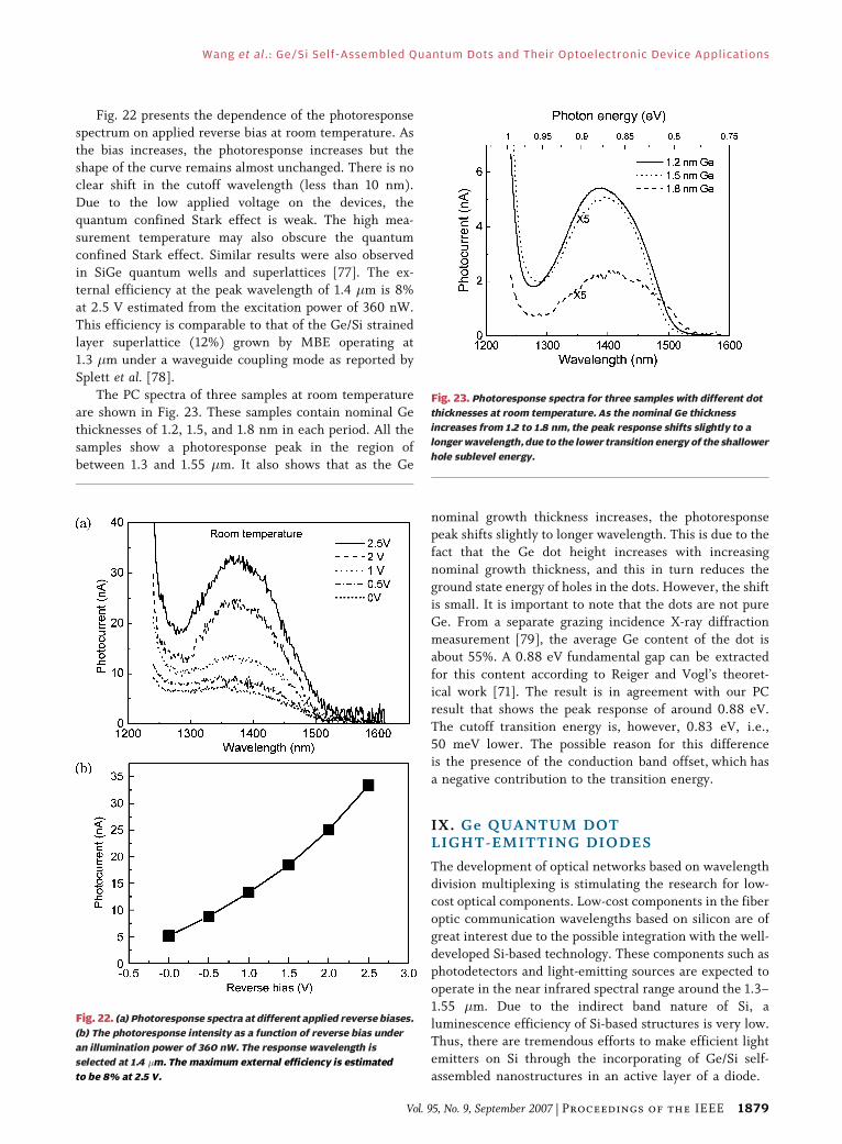
Fig. 22 presents the dependence of the photoresponsespectrum on applied reverse bias at room temperature. As
the bias increases, the photoresponse increases but the
shape of the curve remains almost unchanged. There is no
clear shift in the cutoff wavelength (less than 10 nm).
Due to the low applied voltage on the devices, the
quantum confined Stark effect is weak. The high mea-
surement temperature may also obscure the quantum
confined Stark effect. Similar results were also observedin SiGe quantum wells and superlattices [77]. The ex-
ternal efficiency at the peak wavelength of 1.4 �m is 8%
at 2.5 V estimated from the excitation power of 360 nW.
This efficiency is comparable to that of the Ge/Si strained
layer superlattice (12%) grown by MBE operating at
1.3 �m under a waveguide coupling mode as reported by
Splett et al. [78].
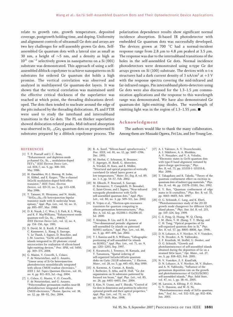
The PC spectra of three samples at room temperatureare shown in Fig. 23. These samples contain nominal Ge
thicknesses of 1.2, 1.5, and 1.8 nm in each period. All the
samples show a photoresponse peak in the region of
between 1.3 and 1.55 �m. It also shows that as the Ge
nominal growth thickness increases, the photoresponse
peak shifts slightly to longer wavelength. This is due to the
fact that the Ge dot height increases with increasing
nominal growth thickness, and this in turn reduces the
ground state energy of holes in the dots. However, the shift
is small. It is important to note that the dots are not pureGe. From a separate grazing incidence X-ray diffraction
measurement [79], the average Ge content of the dot is
about 55%. A 0.88 eV fundamental gap can be extracted
for this content according to Reiger and Vogl’s theoret-
ical work [71]. The result is in agreement with our PC
result that shows the peak response of around 0.88 eV.
The cutoff transition energy is, however, 0.83 eV, i.e.,
50 meV lower. The possible reason for this differenceis the presence of the conduction band offset, which has
a negative contribution to the transition energy.
IX. Ge QUANTUM DOTLIGHT-EMITTING DIODES
The development of optical networks based on wavelength
division multiplexing is stimulating the research for low-cost optical components. Low-cost components in the fiber
optic communication wavelengths based on silicon are of
great interest due to the possible integration with the well-
developed Si-based technology. These components such as
photodetectors and light-emitting sources are expected to
operate in the near infrared spectral range around the 1.3–
1.55 �m. Due to the indirect band nature of Si, a
luminescence efficiency of Si-based structures is very low.Thus, there are tremendous efforts to make efficient light
emitters on Si through the incorporating of Ge/Si self-
assembled nanostructures in an active layer of a diode.
Fig. 22. (a) Photoresponse spectra at different applied reverse biases.
(b) The photoresponse intensity as a function of reverse bias under
an illumination power of 360 nW. The response wavelength is
selected at 1.4 �m. The maximum external efficiency is estimated
to be 8% at 2.5 V.
Fig. 23. Photoresponse spectra for three samples with different dot
thicknesses at room temperature. As the nominal Ge thickness
increases from 1.2 to 1.8 nm, the peak response shifts slightly to a
longer wavelength, due to the lower transition energy of the shallower
hole sublevel energy.
Wang et al. : Ge/Si Self-Assembled Quantum Dots and Their Optoelectronic Device Applications
Vol. 95, No. 9, September 2007 | Proceedings of the IEEE 1879

A p-i-n structure consists of 10-period intrinsicmultilayered Ge quantum dots sandwiched with an n-type
and a p-type Si layers on an n-doped Si (100) substrate. For
this sample, the growth temperature was kept at 550 �C.
After an 100 nm undoped Si buffer layer, a 300 nm nþ Si
layer was grown with an Sb doping concentration of
�2 � 1018 cm�3, followed by a 50 nm intrinsic Si. Then
ten multilayers were grown with an 8 ML Ge layer and an
undoped Si barrier layer of 20 nm thick; after a 100 nmundoped Si space layer a 100 nm pþ Si contact layer was
then grown with a boron doping concentration of
5 � 1018 cm�3. Mesas were defined by optical lithography
and dry etching with CF4=O2 or wet etching with
tetramethylammonium hydroxide (TMAH). The mesa
size is 150 � 300 �m2. A 220 nm SiO2 isolation layer was
deposited by plasma enhanced chemical vapor deposition
(PECVD) and an Al/Ti layer was deposited for contact.The current–voltage characteristics of a typical diode at
room temperature are shown in Fig. 24. A low leakage
current of 3 � 10�5 A/cm2 at �1 V was obtained and the
breakdown voltage was measured to be 7 V at room
temperature. This is similar to the results of obtained by
Splett, where Si/Ge strained layer superlattices were used
instead [78]. Due to high generation rates in Ge, there was
a high leakage current. The electroluminescence (EL) wasexcited with square electrical pulses at a low frequency
with a 1 : 1 duty cycle. A liquid-nitrogen cooled Ge
photodiode was used for EL spectra measurement.
Fig. 25(a) shows EL spectra measured at 77 K as a
function of the current density. The NP-Si peak occurs at
around 1.1 �m, while the peak at about 1.33 �m is due to
the EL from the quantum dots, which may consist of two
peaks of NP and TO-assisted ones. The broad peak at
around 1.48 �m may be due to a radiative intraband
transition [80]. The EL results at room temperature are
shown in Fig. 25(b). The EL peak of 1.33 �m from the
quantum dots is clear. The results demonstrate the fea-
sible application of Ge quantum dots for low-cost optical
emitters operated at the telecommunication wavelengths
and integrated on Si. However, the quantum efficiencywill be still low and hence for practical applications,
research in search for new highly efficient emission
mechanisms remains the most important challenge.
X. SUMMARY
In summary, we have discussed the major issues involved in
the growth, processing, and characterization of Ge dots,interband and intersubband properties of Ge dots, and their
related optoelectronic devices on Si substrates. Self-
assembled and guided Ge quantum dots, and Ge
quantum-dot superlattices grown on Si (100) substrates
were discussed. The morphology of dots was shown to
Fig. 24. Current–voltage characteristics of a Ge dot p-i-n diode at
room temperature. The breakdown voltage is 7 V. The inset gives a
semilog plot of the I–V characteristic, showing clearly a dark current
density of 3 � 10�5 A/cm2 at �1 V.
Fig. 25. Electroluminescence spectra at different biases measured at:
(a) 77 K and (b) 300 K. Electroluminescence from quantum dots was
observed at around 1.33 �m.
Wang et al. : Ge/Si Self-Assembled Quantum Dots and Their Optoelectronic Device Applications
1880 Proceedings of the IEEE | Vol. 95, No. 9, September 2007
relate to growth rate, growth temperature, depositedcoverage, postgrowth holding time, and doping. Uniformity
and alignment controls of ultrasmall Ge dots and arrays are
two key challenges for self-assembly grown Ge dots. Self-
assembled Ge quantum dots with a lateral size as small as
30 nm, a height of �5 nm, and a density as high as
1011 cm�2 selectively grown in nanopatterns on a Si (001)
substrate was demonstrated. This approach of using a self-
assembled diblock copolymer to achieve nanopatterns on Sisubstrates for ordered Ge quantum dot holds a high
promise. The vertical correlation was observed and
analyzed in multilayered Ge quantum-dot layers. It was
shown that the vertical correlation was maintained until
the effective critical thickness of the superlattice was
reached at which point, the threading dislocations devel-
oped. The dots then tended to nucleate around the edge of
the pits induced by the threading dislocations. PL and FTIRwere used to study the interband and intersubband
transitions in the Ge dots. The PL on thicker superlattice
showed dislocation-related peaks. Mid-infrared absorption
was observed in Si1�XGeX quantum dots on prepatterned Si
substrates prepared by a diblock copolymer process. The
polarization dependence results show significant normalincidence absorption. Si-based IR photodetector with
embedded Ge quantum dots was successfully developed.
The devices grown at 700 �C had a normal-incident
response range from 2.8 �m to 4.8 �m peaked at 3.5 �m.
The response was due to the intersubband transitions of the
holes in the self-assembled Ge dots. Normal incidence
photodetectors were demonstrated using n-type Ge dot
arrays grown on Si (100) substrate. The devices with n-i-nstructures had a dark current density of 3 nA/cm2 at þ3 V
with the response spectra covering the mid-infrared and
far-infrared ranges. Pin intersubband photo-detectors using
Ge dots were also discussed for the 1.3–1.5 �m commu-
nication applications and the response to this wavelength
range was demonstrated. We have also demonstrated Ge
quantum-dot light-emitting diodes. The wavelength of
emitting light was in the region of 1.3–1.55 �m. h
Acknowledgment
The authors would like to thank the many collaborators.
Among them are Masaaki Ogawa, Fei Liu, and Joo-Young Lee.
RE FERENCES
[1] T. P. Pearsall and J. C. Bean,BEnhancement- and depletion-modep-channel Gex Si1�x modulation-dopedFET’s,[ IEEE Electron Device Lett.,vol. EDL-7, no. 5, pp. 308–310,May 1986.
[2] H. Daembkes, H.-J. Herzog, H. Jorke,H. Kibbel, and E. Kasper, BThe n-channelSiGe/Si modulation-doped field-effecttransistor,[ IEEE Trans. ElectronDevices, vol. ED-33, no. 5, pp. 633–638,May 1986.
[3] T. Tatsumi, H. Hirayama, and N. Aizaki,BSi/Ge0:3Si0:7/Si heterojunction bipolartransistor made with Si molecular beamepitaxy,[ Appl. Phys. Lett., vol. 52, no. 11,pp. 895–897, Mar. 1988.
[4] D. K. Nayak, J. C. Woo, J. S. Park, K. L. Wang,and K. P. MacWilliams, BEnhancement-modequantum-well Gex Si1�x PMOS,[IEEE Electron Device Lett., vol. 12, no. 4,pp. 154–156, Apr. 1991.
[5] S. David, M. E. Kurdi, P. Boucaud,C. Kammerer, L. Xiang, S. Sauvage,V. Le Thanh, I. Sagnes, D. Bouchier, andJ.-M. Lourtioz, BGe/Si self-assembledislands integrated in 2D photonic crystalmicrocavities for realisation of silicon-basedlight-emitting devices,[ Proc. SPIE, vol. 5450,pp. 369–375, 2004.
[6] G. Masini, V. Cencelli, L. Colace,F. de Notaristefani, and G. Assanto,BLinear array of Si-Ge heterojunctionphotodetectors monolithically integratedwith silicon CMOS readout electronics,[IEEE J. Sel. Topics Quantum Electron., vol. 10,no. 4, pp. 811–815, Jul.–Aug. 2004.
[7] L. Colace, G. Masini, V. O. Cencelli,F. de Notaristefani, and G. Assanto,BPolycrystalline germanium enables near-IRphotodetectors integrated with siliconCMOS electronics,[ Photon. Spectra, vol. 38,no. 12, pp. 88–92, Dec. 2004.
[8] R. A. Soref, BSilicon-based optoelectronics,[Proc. IEEE, vol. 81, no. 12, pp. 1687–1706,Dec. 1993.
[9] M. Herbst, C. Schramm, K. Brunner,T. Asperger, H. Riedl, G. Abstreiter,A. Vorckel, H. Kurz, and E. Muller,BStructural and optical properties of verticallycorrelated Ge island layers grown atlow temperatures,[ Mater. Sci. Eng. B, vol. 89,no. 1–3, pp. 54–57, Feb. 2002.
[10] M. Elkurdi, P. Boucaud, S. Sauvage,O. Kermarrec, Y. Campidelli, D. Bensahel,G. Saint-Girons, and I. Sagnes, BNear-infraredwaveguide photodetector with Ge/Siself-assembled quantum dots,[ Appl. Phys.Lett., vol. 80, no. 3, pp. 509–511, Jan. 2002.
[11] R. Vrijen et al., BElectron-spin-resonancetransistors for quantum computing insilicon-germanium heterostructures,[ Phys.Rev. A, vol. 62, pp. 012306-1–012306-10,Jul. 2000.
[12] T. Kitajima, B. Liu, and S. R. Leone,BTwo-dimensional periodic alignment ofself-assembled Ge islands on patternedSi(001) surfaces,[ Appl. Phys. Lett., vol. 80,no. 3, pp. 497–499, Jan. 2002.
[13] T. I. Kamins and R. S. Williams, BLithographicpositioning of self-assembled Ge islandson Si(001),[ Appl. Phys. Lett., vol. 71, no. 9,pp. 1201–1203, Sep. 1997.
[14] E. Kuramochi, J. Temmyo, H. Kamada, andT. Tamamura, BSpatial ordering ofself-organized InGaAs/AlGaAs quantumdisks on GaAs (311)B substrates,[ J. Electron.Mater., vol. 28, no. 5, pp. 445–451, May 1999.
[15] A. Karmous, A. Cuenat, A. Ronda,I. Berbezier, S. Atha, and R. Hull, BGe dotorganization on Si substrates patterned byfocused ion beam,[ Appl. Phys. Lett., vol. 85,no. 26, pp. 6401–6403, Dec. 2004.
[16] E. Kim, N. Usami, and Y. Shiraki, BControl ofGe dots in dimension and position by selectiveepitaxial growth and their optical properties,[Appl. Phys. Lett., vol. 72, no. 13,pp. 1617–1619, Mar. 1998.
[17] A. I. Yakimov, A. V. Dvurechenskii,A. I. Nikiforov, A. A. Bloshkin,A. V. Nenashev, and V. A. Volodin,BElectronic states in Ge/Si quantum dotswith type-II band alignment initiated byspace-charge spectroscopy,[ Phys.Rev. B, vol. 73, pp. 115333-1–115333-8,Mar. 2006.
[18] T. Takagahara and K. Takeda, BTheory of thequantum confinement effect on excitons inquantum dots of indirect-gap materials,[ Phys.Rev. B, vol. 46, pp. 15578–15581, Dec. 1992.
[19] S. Y. Ren, BQuantum confinement of edgestates in Si crystallites,[ Phys. Rev. B, vol. 55,pp. 4665–4669, Feb. 1997.
[20] O. G. Schimidt, C. Lang, and K. Eberl,BPhotoluminescence study of the 2D-3Dgrowth mode changeover for different Ge/Siisland phases,[ Phys. Stat. Sol. B, vol. 215,pp. 319–324, Sep. 1999.
[21] C. S. Peng, Q. Huang, W. Q. Cheng,J. M. Zhou, Y. H. Zhang, T. T. Sheng, andC. H. Tung, BOptical properties of Geself-organized quantum dots in Si,[ Phys.Rev. B, vol. 57, pp. 8805–8808, Apr. 1998.
[22] D. N. Lobanov, A. V. Novikov, N. V. Vostokov,Y. N. Drozdov, A. N. Yablonskiy,Z. F. Krasilnik, M. Stoffel, U. Denker, andO. G. Schmidt, BGrowth andphotoluminescence of self-assembled islandsobtained during the deposition of Ge on astrained SiGe layer,[ Opt. Mater., vol. 27,no. 5, pp. 818–821, Feb. 2005.
[23] N. V. Vostokov, Z. F. Krasil’nik,D. N. Lobanov, A. V. Novikov, M. V. Shaleev,and A. N. Yablonsky, BInfluence of thegermanium deposition rate on the growthand photoluminescence of Ge(Si)/Si(001)self-assembled islands,[ Phys. Solid State,vol. 47, no. 1, pp. 38–41, 2005.
[24] M. Larsson, A. Elfving, P. O. Holtz,G. V. Hansson, and W.-X. Ni,BPhotoluminescence study of Si/Ge quantumdots,[ Surf. Sci., vol. 532–535, pp. 832–836,Jun. 2003.
Wang et al. : Ge/Si Self-Assembled Quantum Dots and Their Optoelectronic Device Applications
Vol. 95, No. 9, September 2007 | Proceedings of the IEEE 1881

[25] L. Martinelli, A. Marzegalli, P. Raiteri,M. Bollani, F. Montalenti, L. Miglio,D. Chrastina, G. Isella, and H. Kanel,BFormation of strain-induced Si-rich andGe-rich nanowires at misfit dislocationsin SiGe: A model supported byphotoluminescence data,[ Appl. Phys. Lett.,vol. 84, no. 15, pp. 2895–2897, Apr. 2004.
[26] L. Vescan, T. Stoica, O. Chretien, M. Goryll,E. Mateeva, and A. Muck, BSize distributionand electroluminescence of self-assembled Gedots,[ J. Appl. Phys., vol. 87, no. 10,pp. 7275–7282, May 2000.
[27] K. N. Tu, J. W. Mayer, and L. C. Feldman,Electronic Thin Film Science: For ElectricalEngineers and Materials Scientists. New York:Macmillan, 1992, ch. 7, pp. 167–168.
[28] D. J. Eaglesham and M. Cerullo,BDislocation-free Stranski-Krastanow growthof Ge on Si(100),[ Phys. Rev. Lett., vol. 64,pp. 1943–1946, Apr. 1990.
[29] G. Jin, J. L. Liu, and K. L. Wang,BTemperature effect on the formation ofuniform self-assembled Ge dots,[ Appl. Phys.Lett., vol. 83, no. 14, pp. 2847–2849,Oct. 2003.
[30] G. Medeiros-Ribeiro, A. M. Bratkovski,T. I. Kamins, D. A. A. Ohlberg, andR. S. Williams, BShape transition ofgermanium nanocrystals on a silicon (001)surface from pyramids to domes,[ Science,vol. 279, pp. 353–355, Jan. 1998.
[31] R. M. Ross, R. M. Tromp, and M. C. Reuter,BTransition states between pyramids anddomes during Ge/Si island growth,[ Science,vol. 286, pp. 1931–1934, Dec. 1999.
[32] V. A. Shchukin, N. N. Ledentsov, P. S. Kopev,and D. Bimberg, BSpontaneous ordering ofarrays of coherent strained islands,[ Phys. Rev.Lett., vol. 75, pp. 2968–2971, Oct. 1995.
[33] T. I. Kamins, E. C. Carr, R. S. Williams, andS. J. Rosner, BDeposition of three-dimensionalGe islands on Si(001) by chemical vapordeposition at atmospheric and reducedpressures,[ J. Appl. Phys., vol. 81, no. 1,pp. 211–219, Jan. 1997.
[34] K. L. Wang, J. L. Liu, and G. Jin,BSelf-assembled Ge quantum dots on Siand their applications,[ J. Cryst. Growth,vol. 237–239, pp. 1892–1897, Apr. 2002.
[35] J. Drucker and S. Chaparro, BDiffusionalnarrowing of Ge on Si(100) coherent islandquantum dot size distributions,[ Appl. Phys.Lett., vol. 71, no. 5, pp. 614–616, Aug. 1997.
[36] T. I. Kamins, G. Medeiros-Ribeiro,D. Ohlberg, and R. S. Williams, BEvolution ofGe islands on Si(001) during annealing,[ J.Appl. Phys., vol. 85, no. 2, pp. 1159–1171,Jan. 1999.
[37] J. A. Floro, G. A. Lucadamo, E. Chason,L. B. Freund, M. Sinclair, R. D. Twesten, andR. Q. Hwang, BSiGe island shape transitionsinduced by elastic repulsion,[ Phys. Rev.Lett., vol. 80, pp. 4717–4720, May 1998.
[38] F. Boscherini, G. Capellini, L. di Gaspare,F. Rosein, N. Motta, and S. Mobilio, BGe–Siintermixing in Ge quantum dots on Si(001)and Si(111),[ Appl. Phys. Lett., vol. 76, no. 6,pp. 682–684, Feb. 2000.
[39] X. Z. Liao, J. Zou, D. Cockayne, J. Qin,Z. M. Jiang, X. Wang, and R. Leon, BStrainrelaxation by alloying effects in Ge islandsgrown on Si(001),[ Phys. Rev. B, vol. 60,pp. 15 605–15 608, Dec. 1999.
[40] K. Sakamoto, H. Matsuhata, M. O. Tanner,D. Wang, and K. L. Wang, BAlignment ofGe three-dimensional islands on facetedSi(001) surfaces,[ Thin Solid Films, vol. 321,pp. 55–59, May 1998.
[41] Y. H. Xie, S. B. Samavedam, M. Bulsara,T. A. Langdo, and E. A. Fitzgerald, BRelaxedtemplate for fabricating regularly distributedquantum dot arrays,[ Appl. Phys. Lett., vol. 71,no. 24, pp. 3567–3568, Dec. 1997.
[42] S. Y. Shirgaev, E. V. Pedersen, F. Jensen,J. W. Petersen, J. L. Hansen, and A. N. Larsen,BDislocation patterningVA new tool forspatial manipulation of Ge islands,[ Thin SolidFilms, vol. 294, pp. 311–314, Feb. 1997.
[43] Q. Xie, A. Madhukar, P. Chen, andN. P. Kobayashi, BVertically self-organizedInAs quantum box islands on GaAs(100),[Phys. Rev. Lett., vol. 75, pp. 2542–2545,Sep. 1995.
[44] C. Teichert, J. Tersoff, and M. G. Lagally,BStress-induced self-organization of nanoscalestructures in SiGe/Si multilayer films,[Phys. Rev. B, vol. 53, pp. 16 334–16 337,Jun. 1996.
[45] G. Jin, J. L. Liu, S. G. Thomas, Y. H. Luo,K. L. Wang, and B. Y. Nguyen, BControlledarrangement of self-organized Ge islands onpatterned Si (001) substrates,[ Appl. Phys.Lett., vol. 75, no. 18, pp. 2752–2754,Nov. 1999.
[46] G. Jin, J. L. Liu, and K. L. Wang, BRegimentedplacement of self-assembled Ge dots onselectively grown Si mesas,[ Appl. Phys. Lett.,vol. 76, no. 24, pp. 3591–3593, Jun. 2000.
[47] R. R. Li, P. D. Dapkus, M. E. Thompson,W. G. Jeong, C. Harrison, P. M. Chaikin,R. A. Register, and D. H. Adamson, BDensearrays of ordered GaAs nanostructures byselective area growth on substrates patternedby block copolymer lithography,[ Appl. Phys.Lett., vol. 76, no. 13, pp. 1689–1691,Mar. 2000.
[48] Z. M. Zhao, T. S. Yoon, W. Feng, B. Y. Li,J. H. Kim, J. Liu, O. Hulko, Y. H. Xie,H. M. Kim, K. B. Kim, K. L. Wang, C. Ratsch,R. Caflisch, D. Y. Ryu, and T. P. Russell, BThechallenges in guided self-assembly of Ge andInAs quantum dots on Si,[ Thin Solid Films,vol. 508, pp. 195–199, Jun. 2006.
[49] D. Cha, M. Ogawa, C. Chen, S. Kim, J. Lee,K. L. Wang, J. Wang, and T. P. Russell,BIntersubband absorption in p-type Si1�xGex
quantum dots on pre-patterned Si substratesmade by a diblock copolymer process,[J. Cryst. Growth, vol. 301–302, pp. 833–836,Apr. 2007.
[50] D. Y. Ryu, K. Shin, E. Drokenmuller,C. J. Hawker, and T. P. Russell, BAgeneralized appproach to the modification ofsolid surfaces,[ Science, vol. 308,pp. 236–239, Apr. 2005.
[51] P. Mansky, Y. Liu, E. Huang, T. P. Russell,and C. Hawker, BControlling polymer-surfaceinteractions with random copolymerbrushes,[ Science, vol. 275, pp. 1458–1460,Mar. 1997.
[52] O. G. Schmidt, O. Kienzle, Y. Hao, K. Eberl,and F. Ernst, BModified Stranski–Krastanovgrowth in stacked layers of self-assembledislands,[ Appl. Phys. Lett., vol. 74, no. 9,pp. 1272–1274, Mar. 1999.
[53] C. Teichert, M. G. Lagally, L. J. Peticolas,J. C. Bean, and J. Tersoff, BStress-inducedself-organization of nanoscale structures inSiGe/Si multilayer films,[ Phys. Rev. B,vol. 53, pp. 16 334–16 337, Jun. 1996.
[54] J. Tersoff, C. Teichert, and M. G. Lagally,BSelf-organization in growth of quantum dotsuperlattices,[ Phys. Rev. Lett., vol. 76,pp. 1675–1678, Mar. 1996.
[55] B. Rahmati, W. Jaeger, H. Trinkaus, R. Loo,L. Vescan, and H. Lueth, BVertical ordering ofislands in Ge-Si multilayers,[ Appl. Phys. A,vol. 62, pp. 575–579, 1996.
[56] O. Kienzle, F. Ernst, M. Ruhle, O. G. Schmidt,and K. Eberl, BGermanium Fquantum dots_embedded in silicon: Quantitative study ofself-alignment and coarsening,[ Appl. Phys.Lett., vol. 74, no. 2, pp. 269–271, Jan. 1999.
[57] R. People and J. C. Bean, BCalculation ofcritical layer thickness versus latticemismatch for GexSi1�x/Si strained-layerheterostructures,[ Appl. Phys. Lett.,vol. 47, no. 3, pp. 322–324, Aug. 1985.
[58] C. G. van de Walle and R. M. Martin,BTheoretical study of Si/Ge interfaces,[J. Vac. Sci. Technol. B, vol. 3, pp. 1256–1259,Jul./Aug. 1985.
[59] F. Liu, S. Tong, J. Liu, and K. L. Wang,BNormal incident mid-infrared Ge quantumdot photodetector,[ J. Electron. Mater., vol. 33,no. 8, pp. 846–850, 2004.
[60] Y. Y. Lin and J. Singh, BTheory of polarizationdependent intersubband transitions in p-typeSiGe/Si self-assembled quantum dots,[ J. Appl.Phys., vol. 96, no. 2, pp. 1059–1063, Jul. 2004.
[61] U. Bockelmann and G. Bastard, BPhononscattering and energy relaxation in two-, one-,and zero-dimensional electron gases,[ Phys.Rev. B, vol. 42, pp. 8947–8951, Nov. 1990.
[62] J. Phillips, K. Kamath, and P. Bhattacharya,BFar-infrared photoconductivity inself-organized InAs quantum dots,[ Appl.Phys. Lett., vol. 72, no. 16, pp. 2020–2022,Apr. 1998.
[63] N. Rappaport, E. Finkman, T. Brunhes,P. Boucaud, S. Sauvage, N. Yam, V. Le Thanh,and D. Bouchier, BMidinfraredphotoconductivity of Ge/Si self-assembledquantum dots,[ Appl. Phys. Lett., vol. 77,no. 20, pp. 3224–3226, Nov. 2000.
[64] T. Fromherz, W. Mac, A. Hesse, G. Bauer,C. Miesner, K. Brunner, and G. Abstreiten,BIntraband absorption and photocurrentspectroscopy of self-assembled p-type Si/SiGequantum dots,[ Appl. Phys. Lett., vol. 80,no. 12, pp. 2093–2095, Mar. 2002.
[65] C. Miesner, O. Rothig, K. Brunner, andG. Abstreiter, BIntra-valence bandphotocurrent spectroscopy of self-assembledGe dots in Si,[ Appl. Phys. Lett., vol. 76, no. 8,pp. 1027–1029, Feb. 2000.
[66] M. S. Hegazy, T. F. Refaat, M. N. Abedin, andH. E. Elsayed-Ali, BFabrication of Ge/Siquantum-dot infrared photodetector bypulsed laser deposition,[ Optical Engineering,vol. 44, no. 5, pp. 59702-1–59702-3,May 2005.
[67] S. Tong, J.-Y. Lee, H.-J. Kim, F. Liu, andK. L. Wang, BGe dot mid-infraredphotodetectors,[ Opt. Mater., vol. 27, no. 5,pp. 1097–1100, Feb. 2005.
[68] B. F. Levine, BQuantum-well infraredphotodetectors,[ J. Appl. Phys., vol. 74, no. 8,pp. R1–R81, Oct. 15, 1993.
[69] W. Heiss, E. Gornik, H. Hertle, B. Murdin,G. M. H. Knippels, C. J. G. M. Langerak,F. Schaffler, and C. R. Pidgeon,BDetermination of the intersubband lifetimein Si/SiGe quantum wells,[ Appl. Phys. Lett.,vol. 66, no. 24, pp. 3313–3315, Jun. 1995.
[70] I. Bormann, K. Brunner, S. Hackenbuchner,G. Abstreiter, S. Schmult, andW. Wegscheider, BNonradiative relaxationtimes in diagonal transition Si/SiGe quantumcascade structures,[ Appl. Phys. Lett.,vol. 83, no. 26, pp. 5371–5373, Dec. 2003.
[71] M. M. Rieger and P. Vogl, BElectronic-bandparameters in strained Si1�xGex alloys onSi1�yGey substrates,[ Phys. Rev. B,vol. 48, pp. 14 276–14 287, Nov. 1993.
[72] C. Chen, D. Cha, J. Lee, H. Kim, F. Liu,S. Tong, K. L. Wang, J.-Y. Wang, and
Wang et al. : Ge/Si Self-Assembled Quantum Dots and Their Optoelectronic Device Applications
1882 Proceedings of the IEEE | Vol. 95, No. 9, September 2007

T. P. Russell, BNano-patterned growth of Gequantum dots for infrared detectorapplications,[ Proc. Mater. Res. Soc. Symp.,vol. 891, pp. 0891-EE06-01.1–0891-EE06-01.6,2006.
[73] D. D. Coon and R. P. G. Karunasiri, BNewmode of IR detection using quantum wells,[Appl. Phys. Lett., vol. 45, no. 6, pp. 649–651,Sep. 1984.
[74] L. C. West and S. J. Eglash, BFirst observationof an extremely large-dipole infraredtransition within the conduction band of aGaAs quantum well,[ Appl. Phys. Lett., vol. 46,no. 12, pp. 1156–1158, Jun. 1985.
[75] K. L. Wang and R. P. G. Karunasiri, BInfrareddetectors using SiGe/Si quantum wellstructures,[ in Semiconductor Quantum Wells
and Superlattices for Long-Wavelength InfraredDetectors, M. O. Manasreh, Ed. Norwood,MA: Artech House, 1993.
[76] J. Wan, G. L. Jin, Z. M. Jiang, Y. H. Luo,J. L. Liu, and K. L. Wang, BBand alignmentsand photon-induced carrier transfer fromwetting layers to Ge islands grown onSi(001),[ Appl. Phys. Lett., vol. 78, no. 12,pp. 1763–1765, Mar. 2001.
[77] J. Y. Kim, S. Fukatsu, N. Usami, andY. Shiraki, BField-driven blue shift ofexcitonic photoluminescence in Si-Gequantum wells and superlattices,[ J. Cryst.Growth, vol. 157, pp. 40–44, Dec. 1995.
[78] A. Splett, T. Zinke, K. Petermann, E. Kasper,H. Kibbel, H.-J. Herzog, and H. Presting,BIntegration of waveguides and
photodetectors in SiGe for 1.3 �m operation,[IEEE Photon. Technol. Lett., vol. 6, no. 1,pp. 59–61, Jan. 1994.
[79] Z. M. Jiang, X. M. Jiang, W. R. Jiang, Q. J. Jia,W. L. Zheng, and D. C. Qian, BLattice strainsand composition of self-organized Ge dotsgrown on Si(001),[ Appl. Phys. Lett., vol. 76,no. 23, pp. 3397–3399, Jun. 2000.
[80] W. Haecker, BInfrared radiation frombreakdown plasmas in Si, GaSb, and Ge:Evidence for direct free hole radiation,[Phys. Stat. Sol. (a), vol. 25, pp. 301–310,Sep. 1974.
ABOUT T HE AUTHO RS
Kang L. Wang (Fellow, IEEE) received the B.S.
degree from National Cheng Kung University,
China, in 1964, and the M.S. and Ph.D. degrees
from the Massachusetts Institute of Technology
(MIT), Cambridge, in 1966 and 1970, respectively.
From 1970 to 1972, he was an Assistant
Professor at MIT. From 1972 to 1979, he worked
at the General Electric Corporate Research and
Development Center as a Physicist/Engineer. In
1979, he joined the Electrical Engineering Depart-
ment, University of California, Los Angeles (UCLA), where he is currently
Raytheon Chair Professor of Physical Electronics. He also served as Chair
of the Department of Electrical Engineering at UCLA from 1993 to 1996.
He also serves as the Director of the FCRP Focus Center on Functional
Engineered Nano ArchitectonicsVFENA, an interdisciplinary research
center. He was also named the Director of the Western Institute of
Nanoelectronics (WIN), a coordinated multiproject research institute with
UCLA, Stanford University, UC Berkeley, and UC Santa Barbara. He was
also the founding director of Nanoelectronics Research Facility at UCLA
(established in 1989) with the infrastructure to further research in
nanotechnology. His research interests include semiconductor nanode-
vices and nanotechnology; self-assembly growth of quantum structures
and cooperative assembly of quantum-dot arrays; Si-based molecular
beam epitaxy, quantum structures, and devices; nanoepitaxy of
heterostructures; spintronics materials and devices; eand SiGe MBE
and quantum structures. He holds 17 patents and has published over
300 papers.
Dr. Wang has received many awards, including the IBM Faculty Award;
Guggenheim Fellowship; TSMC Honor Lectureship Award; Honoris Causa
at Politechnico University, Torino, Italy; Semiconductor Research Corpo-
ration Inventor Award; and a Semiconductor Research Corporation
Technical Excellence Achievement Award. He serves on the editorial
board of the Encyclopedia of Nanoscience and Nanotechnology (New
York: American Scientific). He is a Senior Editor for the IEEE TRANSACTIONS
ON NANOTECHNOLOGY, and a Series Editor of Nanoscience and Nanotech-
nology for Artech House.
Dongho Cha received the B.S. degree in physics
from Sungkyunkwan University, Korea, in 1990
and the M.S. degree in physics from Pohang
University of Science and Technology (POSTECH),
Korea, in 1995. He is currently working toward the
Ph.D. degree in electrical engineering at the
University of California, Los Angeles (UCLA).
From 1995 to 2002, he worked for Samsung
Electronics as a Senior Engineer. His research
interests include quantum dots, photo detectors,
nanoelectronics, and optoelectronics.
Jianlin Liu received the B.S. and Ph.D. degrees in
physics from Nanjing University, China, in 1993
and 1997, respectively, and another Ph.D. degree
in electrical engineering from the University of
California, Los Angeles (UCLA) in 2003.
In March 2003, Liu joined the Department of
Electrical Engineering, University of California,
Riverside, as a member of tenure-track faculty;
currently he is an Assistant Professor. He has
published three book chapters and more than
100 technical papers and conference proceedings. His areas of research
interests include Si- and ZnO-based semiconductor materials growth,
nanostructures fabrication, and nanodevices fabrication for applications
in nanoelectronics and optoelectronics.
Christopher Chen received the B.S. degree in
electrical engineering and computer sciences
from University of California, Berkeley in 2004,
and the M.S. degree in electrical engineering
from University of California, Los Angeles in
2006. His M.S. thesis was on the development
and characterization of Ge quantum dot infrared
photodetectors.
In 2006, he joined the Modeling and Charac-
terization Group at Altera Corporation (San Jose,
CA) where he supports the development of MOSFET models for new FPGA
products.
Wang et al. : Ge/Si Self-Assembled Quantum Dots and Their Optoelectronic Device Applications
Vol. 95, No. 9, September 2007 | Proceedings of the IEEE 1883