gcep distinguished lecture october 2008 third … · gcep distinguished lecture october 2008 third...
TRANSCRIPT

GCEP Distinguished LectureOctober 2008
Third Generation Photovoltaics
Photovoltaics Centre of Excellence supported by the Australian Research Council, the Global Climate and Energy Project and Toyota CRDL
Gavin Conibeer
Deputy DirectorARC Photovoltaics Centre of Excellence
School of Photovoltaics and Renewable energy EngineeringUniversity of New South Wales

School of Photovoltaics & RE Eng.
Stuart Wenham, Martin Green+ Management Committee
LaboratoriesMark Silver
1st Generation:Wafers
2nd Generation:Thin Films
3rd Generation: PVHigh eff and thin film
Silicon PhotonicsSi light emission
Corodination of previously separately funded strands
Laboratory DevelopmentPV and Renewable Energy U/G degrees
ARC Photovoltaics Centre of Excellence
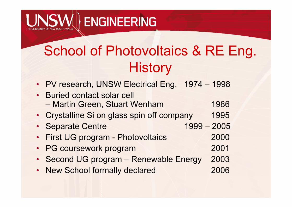
School of Photovoltaics & RE Eng.History
• PV research, UNSW Electrical Eng. 1974 – 1998• Buried contact solar cell
– Martin Green, Stuart Wenham 1986• Crystalline Si on glass spin off company 1995• Separate Centre 1999 – 2005• First UG program - Photovoltaics 2000• PG coursework program 2001• Second UG program – Renewable Energy 2003• New School formally declared 2006

UNSW International Collaborations
•DARPA & U. Delaware (50% efficient solar cell)•Global Climate & Energy Project, Stanford (1)•Global Climate & Energy Project, Stanford (2)•Toyota Central R&D Labs.•Suntech, Wuxi (NYSE)•Nanjing PV Tech, Nanjing (NASDAQ)•JA Solar, Ningjin (NASDAQ)•E-Ton Solar, Taiwan•Asia-Pacific Partnership (Australia, China, India, Japan, Korea, India, USA)
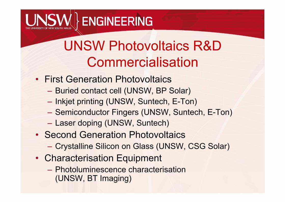
UNSW Photovoltaics R&D Commercialisation
• First Generation Photovoltaics– Buried contact cell (UNSW, BP Solar)– Inkjet printing (UNSW, Suntech, E-Ton)– Semiconductor Fingers (UNSW, Suntech, E-Ton)– Laser doping (UNSW, Suntech)
• Second Generation Photovoltaics– Crystalline Silicon on Glass (UNSW, CSG Solar)
• Characterisation Equipment– Photoluminescence characterisation
(UNSW, BT Imaging)

Undergraduate EducationTwo 4-year Engineering programs (189 students):• Photovoltaics and Solar Energy (2000) (101 students)• Renewable Energy (2003) (88 students)
UAI Distribution 2000-2005
0
10
20
30
40
50
60
70
Below 80 80-84.99 85-89.99 90-94.99 95-100
University Admission Index
# St
uden
ts
3656
3655
3657
3642

Postgraduate Education
• Master of Engineering Science in Photovoltaics and Solar Energy (14 students)– 1.5 year addition to UG;– PV devices; PV systems;
RE technologies;
• Research degrees– PhD (47 students)
– MPhil (10 students)

UNSW Centre for Energy and Environmental Markets
• Interdisciplinary research in energy and environmental markets, policy
• Faculties of Engineering and Commerce & Economics• Environmental sustainability:
– eg. PV load & pricing at Olympic Village• Economic tools & climate change:
– e.g. Market design (Aust. Stock Exchange, CSIRO)• Sustainable technology:
– e.g. Stochastic renewable energy (wind).• Aust. Greenhouse Office

Third Generation PhotovoltaicsOutline
• The importance of Photovoltaics• Three generations of Photovoltaics• The main losses in photovoltaic cells• Third Generation approaches
• Silicon nanostructure tandem cells• Band gap engineering – quantum confinement• Fabrication of materials / devices
• Hot Carrier cells• Contacts – energy filtering • Hot Carrier cooling – energy loss to phonons
• Modification of the solar spectrum• Up- and Down-conversion
• Potentialities and Viabilities• Summary

Transforming the global energy mix: The exemplary path until 2050/ 2100appointed for a term of four years by the federal cabinet (Bundeskabinett)
Meeting the IPCC target of 60% reduction in GHG emission by 2050
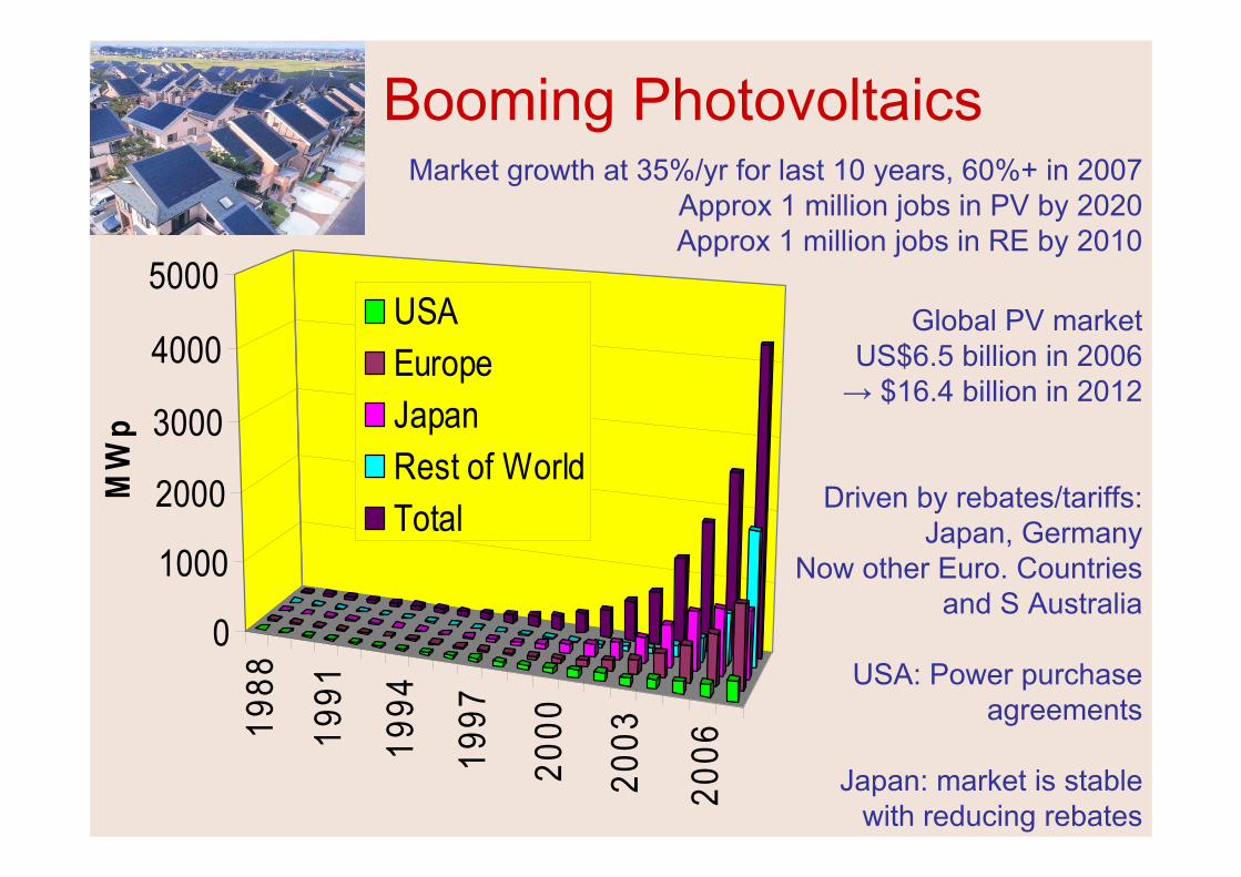
Booming Photovoltaics
Global PV market US$6.5 billion in 2006 → $16.4 billion in 2012
Market growth at 35%/yr for last 10 years, 60%+ in 2007Approx 1 million jobs in PV by 2020Approx 1 million jobs in RE by 2010
Driven by rebates/tariffs: Japan, Germany
Now other Euro. Countries and S Australia
USA: Power purchase agreements
Japan: market is stablewith reducing rebates
1988
1991
1994
1997
2000
2003
2006
0
1000
2000
3000
4000
5000
MW
p
USAEuropeJapanRest of WorldTotal

Learning curves
bulk-Si(~10%)
2003
US
$ /kW (~20%)
20000
10000
5000
2000
1000
500
2000.01 0.1 1.0 10.0 100.0
Gas turbines (USA)
1980
1963
1982
19871993
2001
Wind turbines
2002
Cumulative GW installed
1981
Photovoltaics
. more potential for learning
. lower cost at smaller volumes
20000
10000
5000
2000
1000
500
2000.01 0.1 1.0 10.0 100.0
2002
Cumulative GW installed
1981
Photovoltaics
bulk-Si(~10%)
2003
US
$/kW (~20%)
Thin-film PV
2nd Generation
2002
3rd Generation
1st Generation

100
80
60
20
0 100 200 300 400 500
US$0.50/W
US$1.00/W
US$3.50/W
Cost, US$/m2
US$0.10/W US$0.20/W
Present limit
Thermodynamiclimit
40
Effic
ienc
y,%
Photovoltaics: Three Generations
III
III
mc-Si
III-V tandem
c-Si
thin film
a-Si tandem
concentration
*
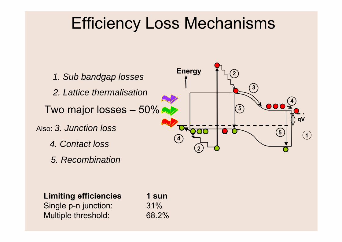
Efficiency Loss Mechanisms
Two major losses – 50%
Limiting efficiencies 1 sunSingle p-n junction: 31%Multiple threshold: 68.2%
qV
2. Lattice thermalisation
2
2
1. Sub bandgap lossesEnergy
3
Also: 3. Junction loss
4
44. Contact loss
5
5
5. Recombination
1

Third generation options
100%
74%68%
54%49%44%39%31%
0%
58%
circulators
tandem (n )hot carrier
impurity PV & band, up-converterstandem (n = 3)thermal, thermoPV, thermionics
impact ionisationtandem (n = 2)down-converterssingle cell
tandem (n = 6)65%
Eg
Eh
Elintermediate level
Ef
Jl
Jh
JVC
CB
VB
Erela
x
h+
e-
e-e-
h+
E0,e
E2,h
E2,e
One photonMultiple electrons-
E0,h
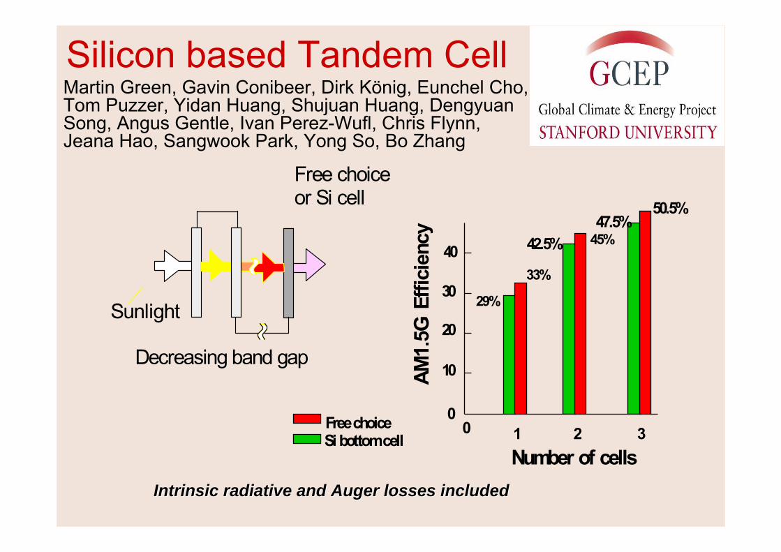
Intrinsic Intrinsic radiativeradiative and Auger losses includedand Auger losses included
Free choiceor Si cell
Decreasing band gap
Sunlight
42.5%47.5%
50.5%
Number of cells1 2 3
10
20
30
40
00
Si bottomcellFreechoice
29%
33%
45%
AM1.
5GEf
ficie
ncy
Silicon based Tandem CellMartin Green, Gavin Conibeer, Dirk König, Eunchel Cho, Tom Puzzer, Yidan Huang, Shujuan Huang, DengyuanSong, Angus Gentle, Ivan Perez-Wufl, Chris Flynn, Jeana Hao, Sangwook Park, Yong So, Bo Zhang
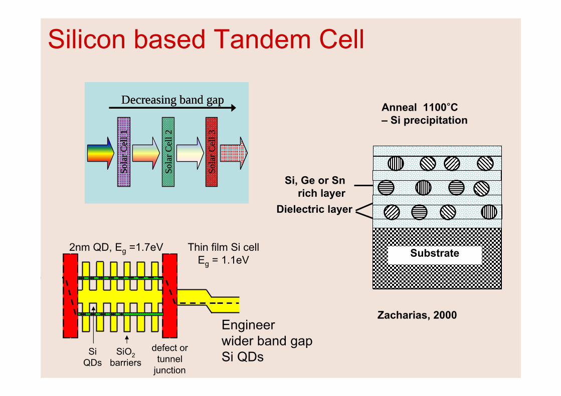
Silicon based Tandem Cell
Sola
r C
ell 1
Sola
r C
ell 2
Sola
r C
ell 3
Decreasing band gap
Sola
r C
ell 1
Sola
r C
ell 2
Sola
r C
ell 3
Decreasing band gap
Zacharias, 2000
Thin film Si cellEg = 1.1eV
2nm QD, Eg =1.7eV
Si QDs
defect or tunnel
junction
SiO2barriers
Engineer wider band gap Si QDs
Anneal 1100°C – Si precipitation
Dielectric layer
Substrate
Si, Ge or Snrich layer
SubstrateSubstrate
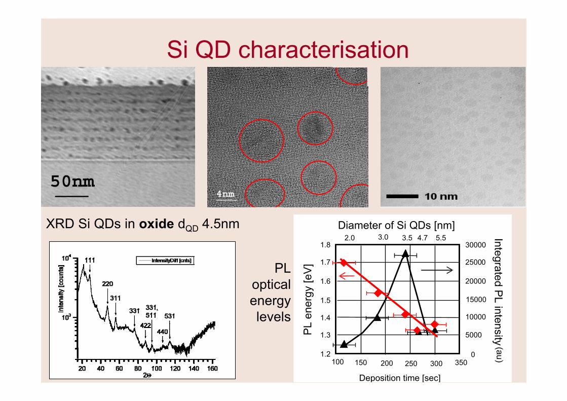
3.02.0 5.54.73.5
100 150 200 250 300 350
Deposition time [sec]
Diameter of Si QDs [nm]
0
0
5000
10000
15000
20000
2500
30000
Integrated PL intensity
(au)1.2
1.3
1.4
1.5
1.6
1.7
1.8
PL
ener
gy [e
V]
Si QD characterisation
XRD Si QDs in oxide dQD 4.5nm
PLoptical energy levels

Range of QD materials
1.0
1.5
2.0
2.5
3.0
3.5
0 1 2 3 4 5 6 7Dot diameter [nm]
PL e
nerg
y [e
V]
Y. Kanemitsu et alH. Takagi et alS. Takeoka et alT. Y. Kim et alT. W. Kim et al Oxide (UNSW) Nitride (UNSW)
Si QDs in oxide/nitride
c-Si
SiC
0.9 eV
1.1 eV
0.5 eV
Si3N4
c-Si
1.9 eV
1.1 eV
2.3 eV
c-Si
SiO2
3.2 eV
1.1 eV
4.7 eV
Alternative matricesGreater σ for Si3N4 but also lower Eact
1.0E-09
1.0E-07
1.0E-05
1.0E-03
1.0E-01
1.0E+01
2.00 2.50 3.00 3.50
1000/T (1/K)
Con
duct
ivity
(S/c
m)
Eσ =0.30eV
Eσ = 0.63eV
Eσ = 0.76eV
Eσ =0.36eV
SiQDs in Si3N4
SiQDs in SiO2
DFT model
-ling

Various material combinationsQuantum Dot / Matrix combinations and current status of investigations
-POSPOSn
--SPGe
SPODSPOEDSPOEDSi
SiCSi3N4SiO2
S = Simulation (ab-initio modelling - DFT)P = Physical (electron microscopy, X-ray difraction)O = Optical (photoluminescence, absorptance)E = Electronic (conductivity, conductivity with Temp.)D = Devices (Diodes, Cells)
Increasing conductivity
Decreasing processing temperature
University of New South Wales, Sydney: Gavin Conibeer, Martin Green, Dirk König, Shujuan Huang, Santosh Shrestha, Chris Flynn, Lara Treiber, Pasquale Aliberti, Andy Hsieh, Rob Patterson, Binesh Puthen Veettil, Martin Kirkengen
Institute Energie Solar, Universitas Polytechnic Madrid: A. Luque, A. Marti, E. Cánovas, A. Martí, P.G. Linares, E. Antolín, D. Fuertes Marrón, C. Tablero
Inst. Research Development Energie Photovoltaic / CNRS, Paris: Jean Francois Guillemoles, Lunmei Huang
University of Sydney: Timothy Schmidt, Raphael Clady, Murad Tayebjee
Hot Carrier solar cellStarted September 2008

Hot Carrier cellExtract hot carriers before they can thermalise:
small Eg
TH
Ef
Hot carrier distribution
• Need to slow carrier cooling
Eδ
Ef(n)
TA
qV=ΔµA
Ese- energy selective contact
h+ energy selective contact
Es
Ef(p)
TA
• Collect carriers over narrow range of energies• Renormalisation of electron (hole) energies
Ross & Nozik, JAP, 53 (1982) 3813Würfel, SOLMAT, 46 (1997) 43 1995Green, 3rd Gen PV (S-Verlag) 2003
Würfel, PIP, 13 (2005) 277Conibeer, TSF, 516(2008) 6948
Takeda et al, SOLMAT, 08

Si QD
Dielectricmatrix
ResonantTransport
Resonant Tunneling Transport
Energy
Energy Selective Contact
Filter
ECEf
Ef
I
V
0
0.01
0.02
0.03
0.04
0 0.5 1 1.5
Gate voltage (V)
Ig(A
) Two different sites on the wafer
NDR at 300K - Repeatable

Hot Carrier cooling
Hot Optical phonon population“phonon bottleneck effect”
Slows further carrier cooling
Decay of Optical phonons to Acoustic is critical
Electrons carry most energy
Cool predominantly via small wave vector optical phonon
emission - timescale of psinelastic – energy relaxation
Optical phonons emitted
Energy

Optical phonon decay

Optical phonon decay
O → LA + LA (Anharmonicity or Klemens mechanism)
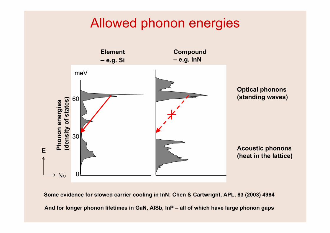
Compound – e.g. InN
Element– e.g. Si
Phon
on e
nerg
ies
(den
sity
of s
tate
s) 60
meV
30
0
Allowed phonon energies
E
Nō
Optical phonons(standing waves)
Acoustic phonons(heat in the lattice)
Some evidence for slowed carrier cooling in InN: Chen & Cartwright, APL, 83 (2003) 4984
And for longer phonon lifetimes in GaN, AlSb, InP – all of which have large phonon gaps

0.0
0.5
1.0
1.5
2.0
2.5
3.0B
iN InN
SnO
GaN
AlS
b
InP
SiC
AlN BN
AlP
0%
20%
40%
60%
80%
100%
Eop
tical−
Eac
oust
icE
acou
stic
Eoptical (M
ax -Min)
Eacoustic
Phononic band-gaps for various binary compounds
Gap > Eacoustic
Gap < Eacoustic
Eg = 0.7eV
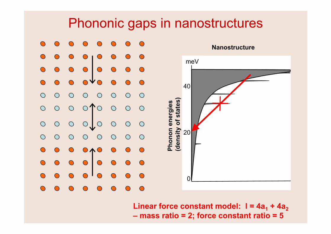
Phononic gaps in nanostructures
Linear force constant model: l = 4a1 + 4a2– mass ratio = 2; force constant ratio = 5
Nanostructure
Phon
on e
nerg
ies
(den
sity
of s
tate
s)
40
meV
20
0
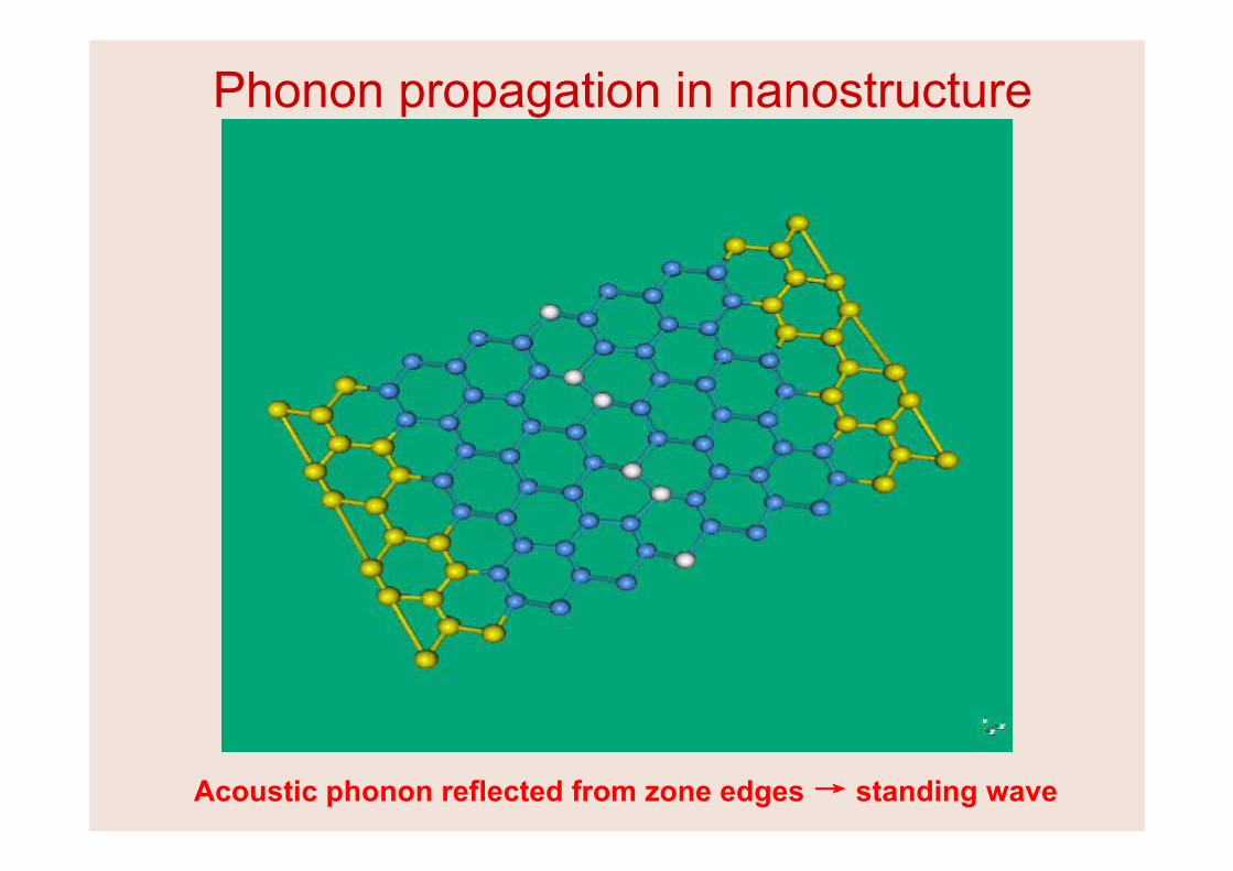
Phonon propagation in nanostructure
Acoustic phonon reflected from zone edges → standing wave
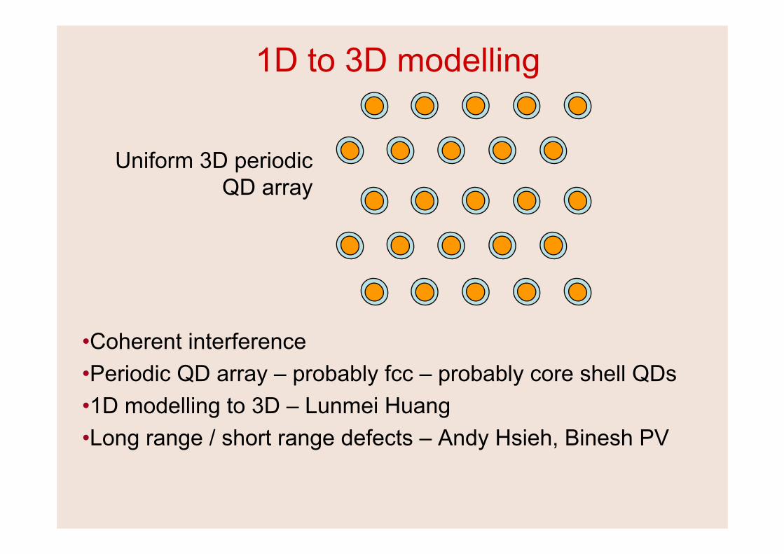
1D to 3D modelling
•Coherent interference •Periodic QD array – probably fcc – probably core shell QDs•1D modelling to 3D – Lunmei Huang•Long range / short range defects – Andy Hsieh, Binesh PV
Uniform 3D periodic QD array
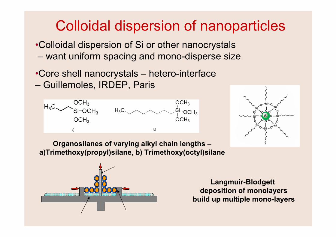
Colloidal dispersion of nanoparticles
•Core shell nanocrystals – hetero-interface – Guillemoles, IRDEP, Paris
•Colloidal dispersion of Si or other nanocrystals– want uniform spacing and mono-disperse size
Langmuir-Blodgett deposition of monolayers
build up multiple mono-layers
Organosilanes of varying alkyl chain lengths –a)Trimethoxy(propyl)silane, b) Trimethoxy(octyl)silane

Towards a complete cell•Fabrication of slowed cooling absorber
•Energy Selective Contacts
•Transport and Renormalisation of carrier energies

PV cell
Modification of the incident solar spectrum
Multiple exciton generation (MEG)Hanna, Nozik, JAP (2006) 100, 074510Schaller, Klimov, PRL (2004) 92, 186601
h+
e-
e-
e-
h+
E0,e
E2,h
E2,e
One photon
Multiple electrons-
E0,h
QE > 100% to be usefuli.e at least as many photons out as in
or: Re-emit two photons above Eg of celleither: Inject two e-h pairs into cell
Down conversion
PbSe QD array by colloidal dispersion

Bifacial solar cell
Reflector
Phosphors in a transparent medium
QE of a few % is usefulEr doped phosphors – Shalav et al., PL (2005) 86, 013505 Triplet - triplet annihilation - Baluschev et al., APL, 90 (2007), 181103
Up Conversion
Up-converter
Solar cell reflector
Eg
Eh
Elintermediate level
Ef
Jl
Jh
JVC
CB
VB
Erelax
Intermediate band solar cellMarti, Luque et al., PRL (2006) 97, 247701.

Potentialities and ViabilitiesRequirements:
Higher efficiencies Lower costReadily available & benign materials
Tandem cellsAlready provenProblems with reducing costNeed breakthrough in cost structure
Thermal approaches - Hot Carrier cellPotentially very high eff. Long way from proof of concept
Up – Down ConversionCan be applied to existing solar cells – big advantageBut early stages of proof of concept
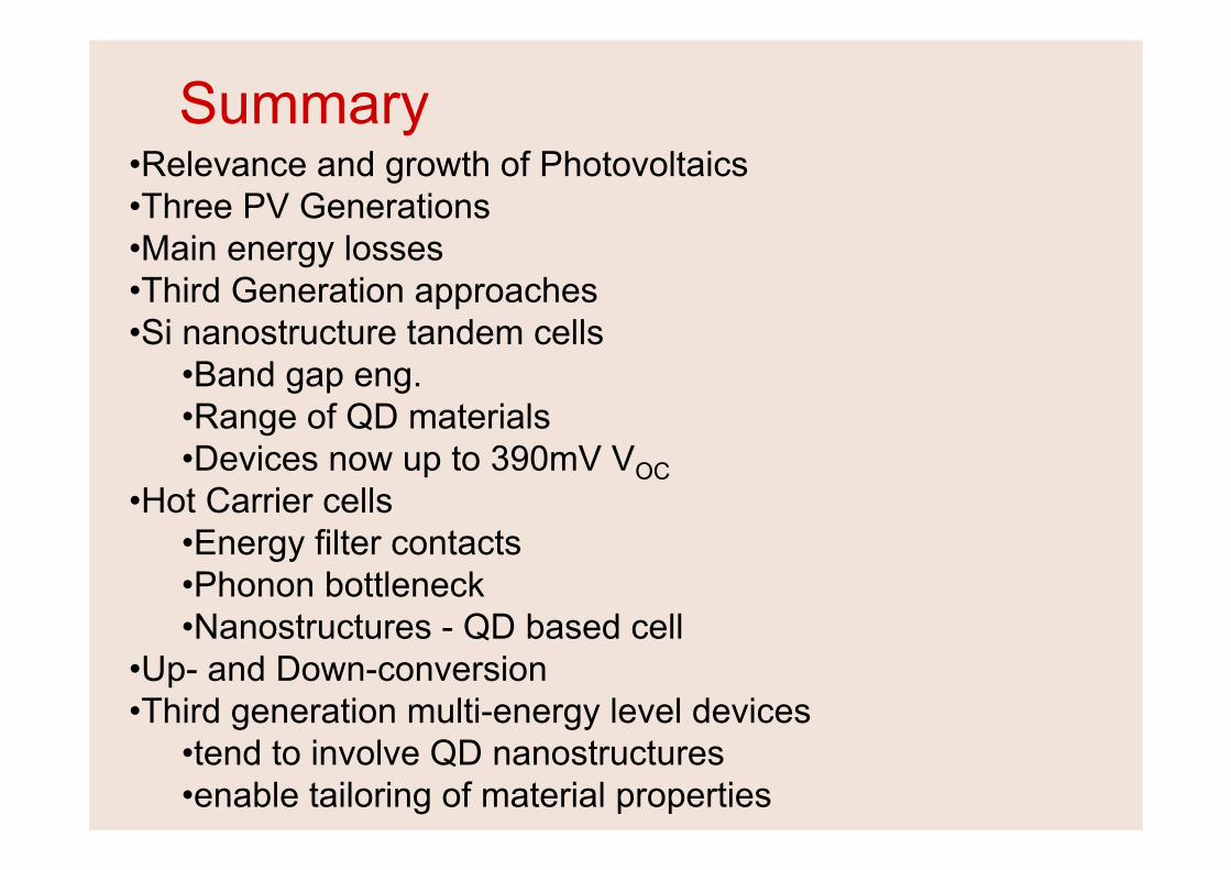
Summary•Relevance and growth of Photovoltaics•Three PV Generations•Main energy losses•Third Generation approaches•Si nanostructure tandem cells
•Band gap eng.•Range of QD materials•Devices now up to 390mV VOC
•Hot Carrier cells•Energy filter contacts•Phonon bottleneck•Nanostructures - QD based cell
•Up- and Down-conversion•Third generation multi-energy level devices
•tend to involve QD nanostructures •enable tailoring of material properties
Research Staff: Martin Green, Richard Corkish, Gavin Conibeer, Dirk König, Eun-ChelCho, Tom Puzzer, Yidan Huang, Shujuan Huang, Dengyuan Song, Santosh Shrestha, Ivan Perez-Wufl, Angus Gentle, Supriya Pillai
PhD students: Chris Flynn, Jeana Hao, Sangwook Park, Lara Treiber, Yong So, Pasquale Aliberti, Yong So, Andy Hsieh, Bo Zhang, Rob Patterson, Binesh Puthen Veettil, Craig Johnson, Darryl Wang, Dawei Dai
Visiting researchers: Fei Gao, Dong-Ho Kim, Frank Koo, Ke Ma, Veronique Gevaerts, Martin Kirkengen, Martina Schmid
Third Generation Strand (2008)
Thank you for your attention