gate – 2015 - career launchermedia.careerlauncher.com/gate-exams/gate actual paper-...
TRANSCRIPT

Q. No. 1 – 5 Car r y One M ar k Each1. What is the adverb for the given word below ?
Misogynous(a) M isogynousness (b) M isogynity(c) M isogynously (d) M isogynous
2. Choose the appropr iate word– phrase out of thefour options given below, to complete the followingsentence.Dhoni, as well as the other ream members ofIndian team present on the occasion(a) Were (b) Was(c) Has (d) Have
3. Ram and Ramesh appeared in an interview fortwo vacancies in the same depar tment . Theprobabil i ty of Ram’s select ion is 1/6 and that ofRamesh is 1/8. What is the probabil i ty that onlyone of them wil l be selected ?
(a)4718
(b)14
(c)1348
(d)3548
4. Choose he word most similar in meaning to thegiven word :
Awkward
(a) Inept (b) Graceful
(c) Suitable (d) Dreadful
5. An electr ic bus has onboard instr uments thatrepor t the total electr ici ty consumed since thestar t of the t r ip as wel l as the total distancecovered. During a single day of operation, the bustravels on stretches M, N, O and P, in that order.The cumulat i ve di st ances t r aveled and thecor responding electr icity consumption are shownin the Table below
St r etch Cum u la t iv e di stance (k m )
E lect r i ci t y used (k Wh)
M 20 12
N 45 25
O 75 45
P 100 57
GENERAL APTI TUDE (GA)
The stretch where the electr icity consumption perkm is minimum is
(a) M (b) N
(c) O (d) P
Q. No. 6 – 10 Car r y Tw o M ar k s Each
6. Given below are two statements fol lowed by twoconclusions. Assuming these statements to betrue, decide which one logical ly fol lows.
St at emen t s :
I . Al l fi lm stars are playback singers.
I I . Al l fi lm directors are fi lm stars
Conclusions :
I . Al l fi lm directors are playback singers.
I I . Some fi lm stars are fi lm directors.
(a) Only conclusion I fol lows
(b) Only conclusion I I fol lows
(c) Neither conclusion I nor I I fol lows
(d) Both conclusions I and I I fol low
7. Lament ing the gradual sidel ining of the ar ts i l lschool cur r icula, a group of prominent ar t istswrote to the Chief M inister last year, asking himto al locate rnore funds to suppor t ar ts educat ionin schools. However, no such increase has beenannounced in this year ’s Budget . The ar t ist sexpressed their deep anguish at their request notbeing appr oved, but many of them r emainopt imist ic about funding in the future
Which of the statement(s) below is/are logical lyval i d and can be i n fer r ed f r om t he abovestatements ?
(i ) The ar t ists expected funding for the ar ts toincrease this year
(i i ) The Chief M inister was recept ive to the ideaof increasing funding for the ar ts
(i i i )The Chief M inister is a prominent ar t ist
(iv) Schools are giving less impor tance to ar tseducat ion nowadays
(a) (i i i ) and (i v) (b) (i ) and (i v)
(c) (i ), (i i ) and (i v) (d) (i ) and (i i i )
GATE – 2015EC : EL ECTRONI CS & COM M UNI CATI ON ENGI NEERI NG
Set - 2N o. of Quest i ons : 65 Maxi mum Mar k s : 100
2 SOLVED PAPER – 2015 (SET - 2)
8. A t iger is 50 leaps of i ts own behind a deer. Thet iger takes 5 leaps per minute to the deer ’s 4. I fthe t iger and the deer cover 8 metre and 5 metreper leap respect ively. What distance in metreswill be tiger have to run before it catches the deer?
9. I f a2 + b2 + c2 = 1, then ab + bc + ac l ies in theinterval
(a)2
1,3
(b)1
, 12
(c)1
1,2
(d) [2, – 4]
10. I n t he fol lowing sentence cer tain par ts ar eunder l ined and marked P, Q and R. One of thepar ts may contain cer tain er ror or may not beacceptable in standard wr it ten communicat ion.Select the par t containing an er ror. Choose D asyour answer i f there is no er ror.
The st uden t cor r ect ed all t he errorsP
t hat
the instructor markedQ
on the answer bookR
(a) P (b) Q
(c) R (d) No er ror
EL ECTRONI CS AND
COM M UNI CATI ON ENGI NEERI NG
Q. No. 1 – 25 Car r y One M ar k Each1. Let the signal f(t) = 0 outside the interval T1, T2,
where T1 and T2 are finite. Furthermore, ( )f t
The region of convergence (RoC) of the signal’sbi lateral Laplace t ransform F(s) is
1. A paral lel st r ip containing the j axis
2. A paral lel st r ip not containing the j axis
3. The ent ire s– plane
4. A half plane containing the j axis
(a) 1 (b) 2
(c) 3 (d) 4
2. A unity negat ive feedback system has an open–
loop t ransfer funct ion G(s) = K .
10s s The gain
K for the system to have a damping rat io of 0.25is .
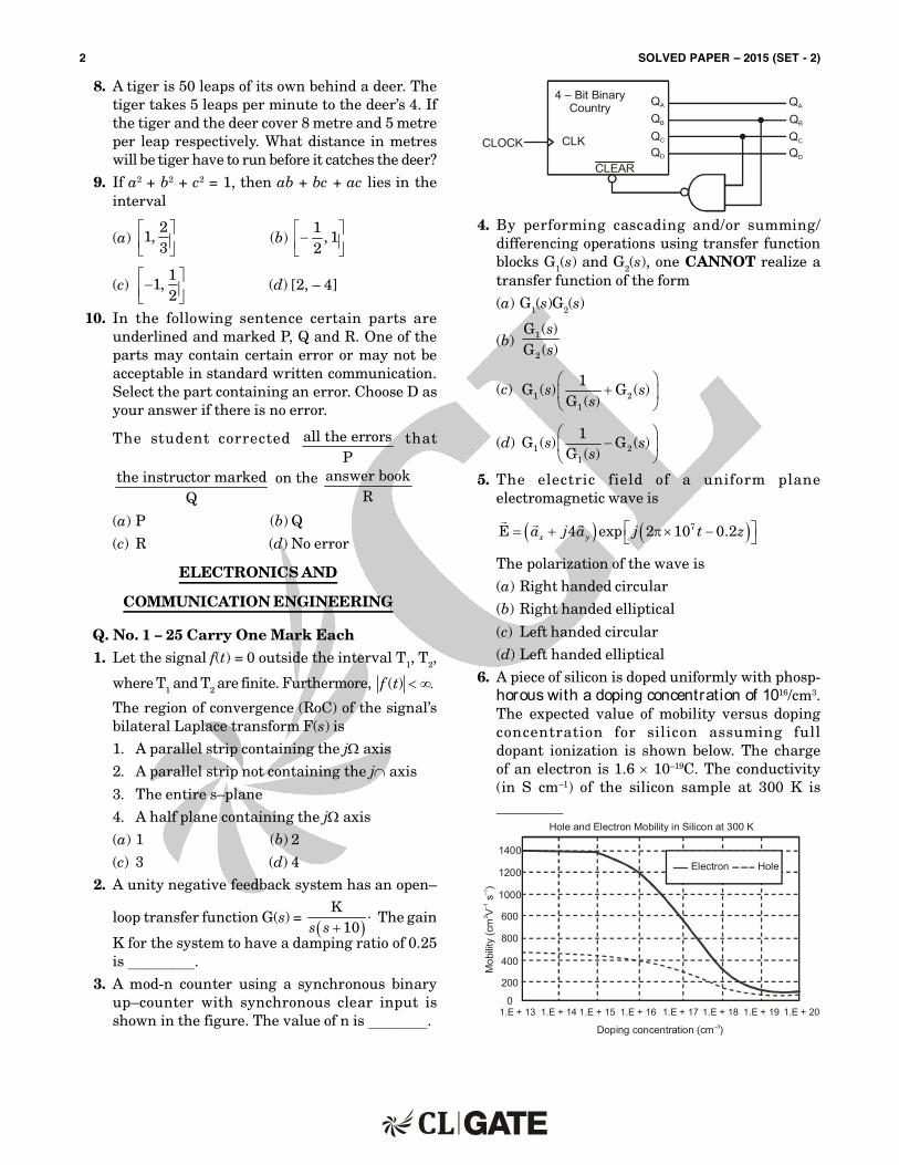
3. A mod-n counter using a synchr onous binaryup– counter wi th synchr onous clear input isshown in the figure. The value of n is .
QA
QB
QC
QD
QA
QB
QC
QD
CLEAR
CLK
4 – Bit BinaryCountry
CLOCK
4. By per for ming cascading and/or summing/differencing operat ions using t ransfer funct ionblocks G1(s) and G2(s), one CANNOT real ize atransfer funct ion of the form
(a) G1(s)G2(s)
(b) 1
2
G ( )G ( )
ss
(c) 1 21
1G ( ) G ( )
G ( )s s
s
(d) 1 21
1G ( ) G ( )
G ( )s s
s
5. The el ect r i c f i el d of a un i for m pl aneelectromagnet ic wave is
7E 4 exp 2 10 0.2x ya j a j t z
The polar izat ion of the wave is
(a) Right handed circular
(b) Right handed el l ipt ical
(c) Left handed circular
(d) Left handed el l ipt ical
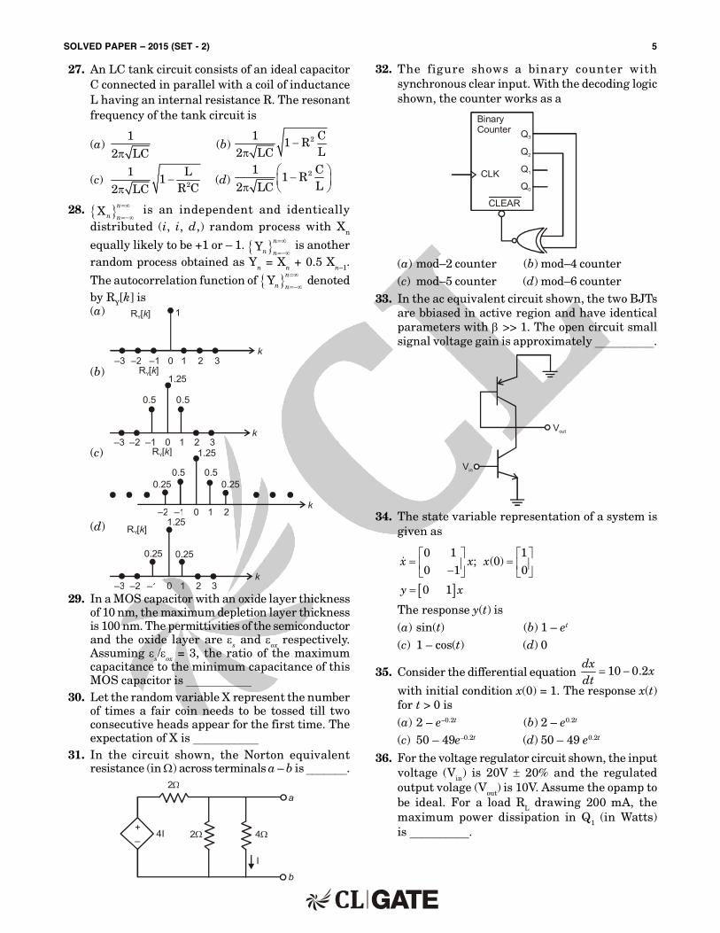
6. A piece of si l icon is doped uniformly with phosp-horous with a doping concentration of 1016/cm3.The expected value of mobil i ty versus dopingconcen t r at i on for si l i con assumi ng fu l ldopant ionizat ion is shown below. The chargeof an electron is 1.6 10– 19C. The conduct ivity(in S cm – 1) of the si l icon sample at 300 K is
Electron Hole1400
1200
1000
600
800
400
200
01.E + 13 1.E + 14 1.E + 15 1.E + 16 1.E + 17 1.E + 18 1.E + 19 1.E + 20
Doping concentration (cm )–3
Hole and Electron Mobility in Silicon at 300 K
Mob
ility
(cm
V s
)2
–1–1
SOLVED PAPER – 2015 (SET - 2) 3
7. I n the figure shown, the output Y is required tobe Y AB CD. The gates G1 and G2 must be,respect ively,
A
B
CD
G1
G2 Y
(a) NOR, OR (b) OR, NAND
(c) NAND, OR (d) AND, NAND
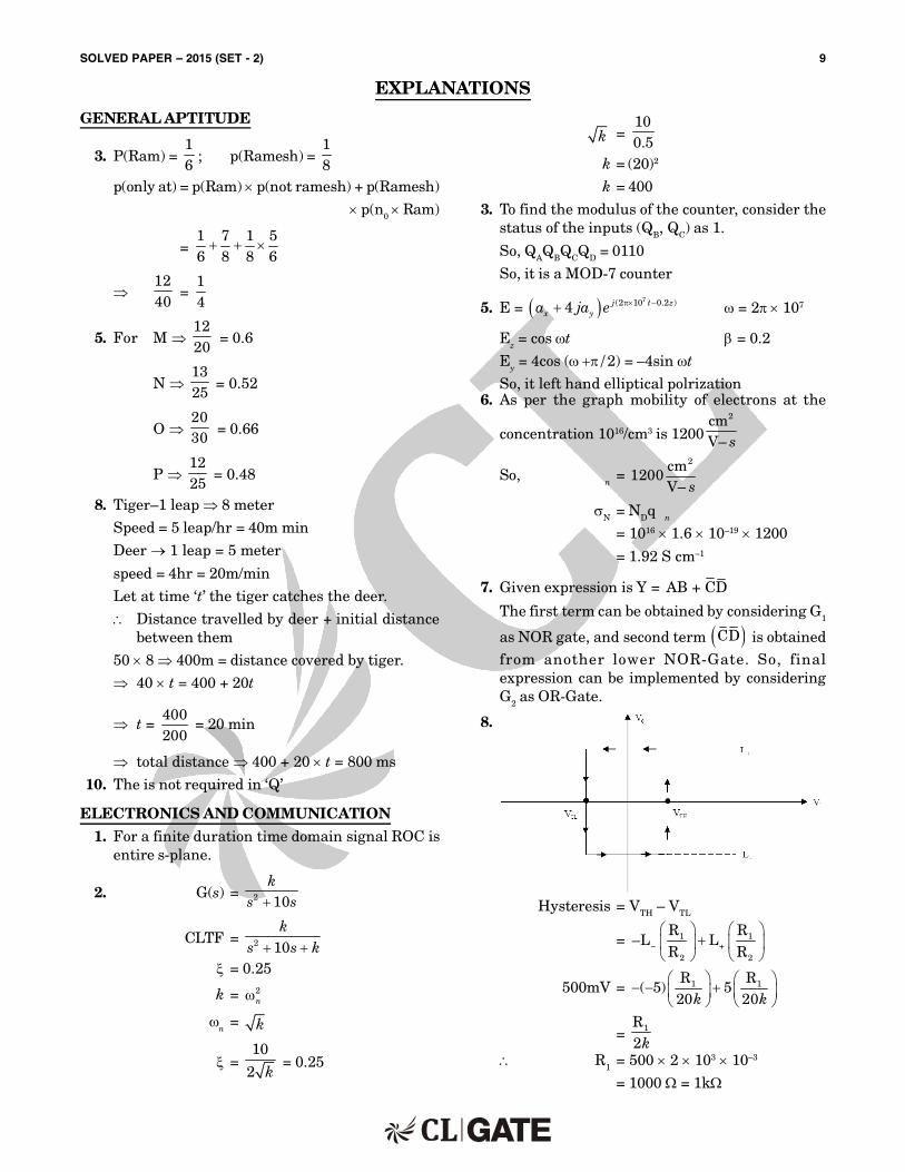
8. I n the bistable circuit shown, the ideal opamphas satur at ion level of 5V. The value of R1
(in k) that gives a hysteresis width of 500 mVis .
+–
+
–Vin
R1
R = 20k2
Vout
9. Two causal discrete– time signal x[n] and y[n] arerelated as 0
nmy n x m
I t the z– t ransform of y[n] is 2
2,
1z z the value
of x[2] is .
10. The bi lateral Laplace t ransform of a funct ion
1 if( )
0 otherwise
a t bf t
(a)a b
s
(b) 2e a b
s
(c)as bse e
s
(d)
( )s a bes
11. The 2– por t admi t tance mat r ix of the ci r cui tshown is given by
10 10
5
(a)0.3 0.2
0.2 0.3
(b)15 5
5 15
(c)3.33 5
5 3.33
(d)0.3 0.4
0.4 0.3
12. The value of x for which al l the eigen– values ofthe matr ix given below are real is
10 5 4
20 2
4 2 10
j
x
(a) 5 + j (b) 5 – j
(c) 1 – 5j (d) 1 + 5j
13. The signal cos 104
t
is ideally sampled at a
sampling frequency of 15 Hz. The sampled signalis passed through a fi l ter with impulse response
sincos 10
2t
tt
. The fi l ter output is
(a)15
cos 402 4
t
(b) sin15
cos 102 4
tt
t
(c)15
cos 102 4
t
(d) sin15
cos 402 2
tt
t
14. A sinusoidal signal of amplitude A is quant ized
by a uniform quant izer Assume that the signalut i l izes al l t he r epr esentat i on l evel s of t hequantizer. I f the signal to quantization noise rat iois 31.8 dB, the number of levels in the quant izeris
15. The magnitude and phase of the complex Four ierser ies coefficients ak of a per iodic signal x(t) areshown in the figure. Choose the cor rect statementform the four choices given.
Not at i on : C is the set of complex numbers, R isthe set of purely real numbers, and P is the setpurely imaginary numbers.
k0
–
4321–1–2–3–4–5
–1–2–3–4–5 43210ak
k
3 3
22
ak

4 SOLVED PAPER – 2015 (SET - 2)
(a) x(t) R
(b) x(t) P
(c) x(t) (C – R)
(d) The informat ion given is not sufficient to drawany conclusion about x(t)
16. The general solut ion of the different ial equat ion
1 cos21 cos2
dy ydx x
is
(a) tan y – cot x = c (c is a constant)
(b) tan x – cot y = c (c is a constant)
(c) tan y + cot x = c (c is a constant)
(d) tan x + cot y = c (c is a cons tant)
17. An n– type sil icon sample is uniformly il luminatedwith l ight which generates 1020 electron hole pairsper cm3 per second. The minor ity car r ier l i fetimein the sample is 1s . Int eh steady state, the holeconcentrat ion in the sample is approximately 10x,where x is an integer. The value of x is
18. I f the circuit shown has to funct ion as a clampingci rcuit , which one of the fol lowing condi t ionsshould be sat i sf i ed for si nusoidal si gnal ofper iod T ?
RV
C+ –
(a) RC << T (b) RC = 0.35 T
(c) RC T (d) RC >> T
19. I n a sour ce f r ee r egi on i n vacuum, i f t heelectrostat ic potent ial = 2x2 + y2 + cz2, the valueof constant c must be
20. I n an 8085 microprocessor, which one of thefollowing instruct ions changes the content of theaccumulator ?
(a) MOV B, M (b) PCHL
(c) RNZ (d) SBI BEH
21. The voltage (VC) across the capacitor (in Volts) inthe network shown is
80 V 40 V VC
100 V, 50 Hz
22. Let f(z) = .az bcz d
I f f(z1) = f(z2) for al l z1 z2, a = 2,
b = 4 and c = 5, then d should be equal to .
23. I n t he ci r cu i t shown t he aver age value ofthe voltage Vab (in Volts) in steady state condit ionis .
ab 1mH1 F
+–Vab
2k1k
5V
5 sin(5000 ) t
24. For the signal flow graph shown in the figure,
the value of C( )R( )
ss
is
C( )s1 X1 X3 X41
G1 X2 G2 G3 G4X5
–H3
–H2–H1
R( )s
(a) 1 2 3 4
1 2 1 3 4 2 2 3 3 1 2 3 4 1 2
G G GG1 G G H G G H G G H G G G G H H
(b) 1 2 3 4
1 2 1 3 4 2 2 3 3 1 2 3 4 1 2
G G G G1 G G H G G H G G H G G G G H H
(c)1 2 1 3 4 2 2 3 3 1 2 3 4 1 2
11 G G H G G H G G H G G G G H H
(d)1 2 1 3 4 2 2 3 3 1 2 3 4 1 2
11 G G H G G H G G H G G G G H H
25. I n the circuit shown, V0 = V0A for switch SW inposit ion A and V0 = V0B SW in position B. Assume
that the opamp is ideal. The value of 0B
0A
VV
is
1 k
1 k
1 k
1 k
1 k5V
SW
B A
1V
V0
–
+
Q. No. 26 – 55 car r y Tw o M ar k s Each
26. Let X {0, 1) and Y {0, 1} be two independentbinary random var iables. I f P (X = 0) = p andP(Y = 0) = q, then P(X + Y 1) is equal to
(a) pq + (1 – p) (1 – q) (b) pq
(c) p(1 – q) (d) 1 – pq
SOLVED PAPER – 2015 (SET - 2) 5
27. An LC tank circuit consists of an ideal capacitorC connected in paral lel with a coi l of inductanceL having an internal resistance R. The resonantfrequency of the tank circuit is
(a)1
2 LC(b) 21 C
1 RL2 LC
(c) 2
1 L1
R C2 LC
(d)
21 C1 R
L2 LC
28. Xn
n n
i s an i ndependent and i dent ical l y
dist r ibuted (i , i , d ,) r andom pr ocess wi th Xn
equally l ikely to be +1 or – 1. Yn
n n
is another
random process obtained as Yn = Xn + 0.5 Xn– 1.
The autocor relat ion funct ion of Yn
n n
denoted
by RY[k] is(a)
k
1
3210–1–2–3
R [ ]Y k
(b)1.25
0.50.5
R [ ]Y k
k3210–1–2–3
(c)
0.250.5 0.5
0.25
2
1.25
10–1–2
R [ ]Y k
k
(d)
0.250.25
3210–1–2–3
1.25
k
R [ ]Y k
29. I n a MOS capacitor with an oxide layer thicknessof 10 nm, the maximum depletion layer thicknessis 100 nm. The permit tivi t ies of the semiconductorand the oxide layer are s and ox respect ively.Assuming s/ox = 3, the rat io of the maximumcapacitance to the minimum capacitance of thisMOS capacitor is
30. Let the random var iable X represent the numberof t imes a fair coin needs to be tossed t i l l twoconsecut ive heads appear for the first t ime. Theexpectat ion of X is
31. I n the ci r cui t shown, the Nor ton equivalentresistance (in ) across terminals a – b is .
b
4I
I
2 4
2a
+–
32. The f i gu r e shows a bi nar y coun t er w i t hsynchronous clear input . With the decoding logicshown, the counter works as a
BinaryCounter Q3
Q2
Q1
Q0
CLK
CLEAR
(a) mod– 2 counter (b) mod– 4 counter(c) mod– 5 counter (d) mod– 6 counter
33. I n the ac equivalent circuit shown, the two BJTsare bbiased in act ive region and have ident icalparameters with >> 1. The open circuit smallsignal voltage gain is approximately .
Vin
Vout
34. The state var iable representat ion of a system isgiven as
0 1 1; (0)
0 1 0
0 1
x x x
y x
The response y(t) is(a) sin(t) (b) 1 – et
(c) 1 – cos(t) (d) 0
35. Consider the differential equat ion 10 0.2dx
xdt
with init ial condit ion x(0) = 1. The response x(t)for t > 0 is(a) 2 – e– 0.2t (b) 2 – e0.2t
(c) 50 – 49e– 0.2t (d) 50 – 49 e0.2t
36. For the voltage regulator circuit shown, the inputvoltage (V in) is 20V 20% and the r egulatedoutput volage (Vout) is 10V. Assume the opamp tobe ideal. For a load RL drawing 200 mA, themaximum power dissipat ion in Q1 (in Wat ts)is .

6 SOLVED PAPER – 2015 (SET - 2)
37. I nput x(t) and output y(t ) of an LTI system arerelated by the different ial equat ion y(t) – y(t)– 6y(t) = x(t). I f the system is neither causal norstable, the impulse response h(t) of the system is
(a) 3 21 1( ) ( )
5 5t te u t e u t
(b) 3 21 1( ) ( )
5 5t te u t e u t
(c) 3 21 1( ) ( )
5 5t te u t e u t
(d) 3 21 1( ) ( )
5 5t te u t e u t
38. The di ode i n t he ci r cu i t gi ven bel ow hasVON = – 0.7 V but is ideal otherwise. The cur rent(in mA) in the 4k resistor is .
4 k
2 k 3 k
1 k
6 k
D
1mA
39. A zero mean white Gaussian noise having power
spectral density 0N2
is passed through an LTI
fil ter whose impulse response h(t) is shown in thefigur e. The var iance of the fi l t er ed noise att = 4 is
– A
0 1 2 3t
A
h t( )
(a) 20
3A N
2(b) 2
0
3A N
4
(c) A2N 0 (d) 20
1A N
2
40. Assuming that the opamp in the circuit shownbelow is ideal, the output voltage V0 (in volts)is
1V
1 k
2 k
12V
Vo
–
+
–12V
41. A 1 – to – 8 demult iplexer with data input in D in,address inputs S0, S1, S2 (with S0 as the LSB) and
0 7Y to Y as the eight demult iplexed output , is tobe designed using two 2 – to – 4 decoders (withenable input E and address input A0 and A1) asshown in the figure D in, S0, S1 and S2 are to beconnected to P, Q, R and S, but not necessar ily inthis order. The respect ive input connect ions to P,Q, R and S terminals should be
PQR
S
1Y0
1Y1
1Y2
1Y3
Y0
Y1
Y2
Y3
Y4
Y5
Y6
Y7
2Y0
2Y1
2Y2
2Y3
2E
2A0
2A 71
2–to–4Decoder
1E
1A1
1A0
2–to–4Decoder
(a) S2, D in, S0, S1 (b) S1, D in, S0, S2
(c) D in, S0, S1, S2 (d) D in, S2, S0, S1
42. The value of the integral
sin(4 )12cos 2
4t
t dtt
is
43. A funct ion of Boolean var iables X, Y and Z isexpr essed in terms of the min– ter ms as F(X,Y, Z) = (1, 2, 5, 6, 7)
Which one of the product of sums given below isequal to the funct ion F(X, Y, Z) ?
(a) X Y Z X Y Z X Y Z
(b) X Y Z X Y Z X Y Z
(c) X Y Z X Y Z X Y Z
X Y Z X Y Z
(d) X Y Z X Y Z X Y Z
X Y Z X Y Z
SOLVED PAPER – 2015 (SET - 2) 7
44. The t ransfer funct ion of a mass– spr ing dampersystem is given by
G(s) = 2
1M B Ks s
The frequency response data for the system aregiven in the fol lowing table.
in rad/s G in B arg G in deg
0.01 18.5 0.2
0.1 18.5 1.30.2 18.4 2.6
1 16 16.92 11.4 89.4
3 21.5 151
5 32.8 16710 45.3 174.5
j d j
The unit step response of the system approachesa steady state value of
45. Two half– wave dipole antennas placed as shownin the figure are excited with sinusoidally varyingcur rents of frequency 3 MHz and phase shift of/2 between them (the element at the or igin leadsin phase). I f the maximum radiated E– field att he poin t P i n t he x– y pl ane occur s at anazimuthal angle of 60 the distance d (in meters)between the antennas is .
yO
z
d
60°
x
OP >>d
46. An air – fi l led rectangular waveguide of internaldimensions a cm bcm (a > b) has a cutofffrequency of 6 GHz for the dominant TE10 mode.For the same waveguide, i f the cutoff frequencyof the TM 11 mode is 15 GHz, the cutoff frequencyof the TE01 mode in GHz is .
47. Consider two real sequences with t ime– or iginmarked by the bold value
x1[n] = {1, 2, 3, 0}, x2[n] = {1, 3, 2, 1}
Let X1(k) and X2(k) be 4– point DFTs of x1[n] andx2[n], respect ively
Another sequence x3[n ] is der ived by tak ing4– point inverse DFT of x3(k) = x1(k) x2(k).
The value of x3[2] is
48. Let x(t) = as(t) + s (– t) with s(t) = e– 4tu(t), whereu(t) is unit step funct ion. I f the bi lateral Lapalcetransform of x(t) is
2
16X( ) 4 Re{ } 4
16s s
s
Then the value of is
49. Consider a binary, digital communicat ion systemwhich used pulses g(t) and – g(t ) for t ransmit t ingbits over an AWGN channel. I f the receiver usesa matched filter, which one of the following pulseswil l give the minimum probabil i ty of bit er ror ?(a)
t10
1
g t( )
(b)
t10
1
g t( )
(c)
t0 1
g t( )
1
(d)
t10
1
g t( )
50. The electr ic field of a plane wave propagat ing ina lossless non– magnet ic medium is given by thefol lowing expression
E(z, t) = 95cos 2 10 3cosx ya t z a
92 102
t bz
The type of the polar izat ion is
(a) Right Hand Circular
(b) Left Hand Ell ipt ical
(c) Right Hand Ell ipt ical
(d) L inear

8 SOLVED PAPER – 2015 (SET - 2)
51. The energy band diagram and electron densityprofi le n(x) in a semiconductor are shown in the
figure. Assume that n(x) = 3cm
15 T10 ,q xke
with
= 0.1 V/cm and x expressed in cm. Given,
2 1T D T .0.026V, D 36cm , andn
k ks
q q
The electron cur rent density (in A/cm2) at x = 0 is
x = 0 x
Ev
Ec
E(eV)
Slope = – 0.1eV/cm
x = 0 x
log( ( ))n x
(a) – 4.4 10– 2 (b) – 2.2 10– 2
(c) 0 (d) – 4.4 10– 2
52. A dc voltage of 10V is applied across an n– typesil icon bar having a rectangular cross– sect ion anda length of 1cm as shown in figure. The donordoping concent r at ion N D and the mobi l i t y ofel ect r ons n ar e 1016 and 1000 cm 2V – 1s– 1,respect ively. The average t ime (in ms) taken bythe electrons to move from one end of the bar toother end is .
n – Si
1cm
10V
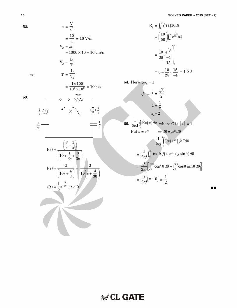
53. I n the circuit shown, the init ial voltages acrosst he capaci t or s C1 and C2 ar e 1V and 3V,respect ively. The switch is closed at t ime t = 0.The total energy dissipated (in Joules) in theresistor R unti l steady state is reached is
+–
C = 1F2C = 3F1
+–
t = 0R = 10
54. The output of a standard second– order systemfor a unit step input is given as
2( ) 1 cos 3
63ty t e t
The t ransfer funct ion of the system is
(a)
2
2 3s s
(b) 2
12 1s s
(c) 2
32 3s s
(d) 2
42 4s s
55. I f C denotes the counterclockwise unit circle, the
value of the contour integral C
1Re
2z dz
j is .
ANSWERS
GENERAL APTI TUDE
1. (c) 2. (b) 3. (b) 4. (a) 5. (d) 6. (d) 7. (b)
8. (800) 9. (b) 10. (b)
ELECTRONI CS AND COM M UNI CATI ON
1. (c) 2. (400) 3. (7) 4. (b) 5. (d) 6. (1.92) 7. (a)
8. (1) 9. (0) 10. (c) 11. (a) 12. (b) 13. (a) 14. (32)
15. (a) 16. (d) 17. (14) 18. (d) 19. (– 3.1)– (– 2.9) 20. (d) 21. (100)
22. (10) 23. (5) 24. (b) 25. (1.5) 26. (d) 27. (b) 28. (b)
29. (4.33) 30. (1.5) 31. (1.333) 32. (c) 33. (– 1) 34. (d) 35. (c)
36. (2.8056) 37. (b) 38. (0.6) 39. (a) 40. (11– 12) 41. (d) 42. (3)
43. (b) 44. (0.12) 45. (50) 46. (13.7) 47. (11) 48. (– 2) 49. (a)
50. (b) 51. (c) 52. (100) 53. (1.5) 54. (d) 55. (0.5)
SOLVED PAPER – 2015 (SET - 2) 9
EXPL ANATI ONS
GENERAL APTI TUDE
3. P(Ram) = 16
; p(Ramesh) = 18
p(only at) = p(Ram) p(not ramesh) + p(Ramesh)
p(n0 Ram)
= 1 7 1 56 8 8 6
1240
= 14
5. For M 1220
= 0.6
N 1325
= 0.52
O 2030
= 0.66
P 1225
= 0.48
8. Tiger – 1 leap 8 meter
Speed = 5 leap/hr = 40m min
Deer 1 leap = 5 meter
speed = 4hr = 20m/min
Let at t ime ‘t’ the t iger catches the deer.
Distance t ravelled by deer + init ial distancebetween them
50 8 400m = distance covered by t iger.
40 t = 400 + 20t
t = 400200
= 20 min
total distance 400 + 20 t = 800 ms
10. The is not required in ‘Q’
ELECTRONI CS AND COM M UNI CATI ON1. For a finite durat ion t ime domain signal ROC is
ent ire s-plane.
2. G(s) = 2 10k
s s
CLTF = 2 10k
s s k = 0.25
k = 2n
n = k
= 10
2 k = 0.25
k = 100.5
k = (20)2
k = 400
3. To find the modulus of the counter, consider thestatus of the inputs (QB, QC) as 1.
So, QAQBQCQD = 0110
So, i t is a MOD-7 counter
5. E = 7(2 10 0.2 )4 j t zx ya ja e = 2 107
Ez = cos t = 0.2
Ey = 4cos (/ 2) = – 4sin t
So, i t left hand el l ipt ical polr izat ion6. As per the graph mobil i ty of electrons at the
concentrat ion 1016/cm3 is 12002cm
V– s
So, µn = 2cm
1200V– s
N = NDqµn
= 1016 1.6 10– 19 1200
= 1.92 S cm– 1
7. Given expression is Y = AB + CD
The first term can be obtained by consider ing G1
as NOR gate, and second term CD is obtained
f r om anot her l ower N OR-Gat e. So, f i nalexpression can be implemented by consider ingG2 as OR-Gate.
8.
Hysteresis = VTH – VTL
= 1 1– +
2 2
R R– L L
R R
500mV = 1 1R R( 5) 5
20 20k k
= 1R2k
R1 = 500 2 103 10– 3
= 1000 = 1k

10 SOLVED PAPER – 2015 (SET - 2)
9. y[n] = 0
[ ]n
m
x m
Accor di ng t o accumu l at i on pr oper t y ofz-transform,
Y[z] = 1
X( )
1
z
z
2
( 1)z z = X( )
( 1)z zz
X[z] =
221
zz
=
3
1
2
1
z
z
x[n] = 2u[n – 3] thus x[2] = 0
10. Given f(t) = 1
0 otherwise
a t b
L{f(t)} = 0
( )ste f t dt
= 0
( ) ( ) ( )st st st
a be f t e f t dt e f t dt
= 0 0b st
ae dt
= st bes a
= 1 bs ase es
= as bse e
s
12. Let A =
10 5 J 4
20 2
4 2 10
x
Given that al l eigen values of A are real.
A is Hermit ian
A = A i .e. TA = A
10 4
5 20 2
4 2 10
x
j
=
10 5 J 4
20 2
4 2 10
x
x = 5 – j
13. Given signal is x(t) = cos 104
t
Neglect the phase-shift 4
and it can be inser ted
at the end result .
I f x1(t) = cos 10t L X1(f)
= 1( 5) ( 5)
2f f
Given fi l ter impulse response is,
h(t) = sin
cos 402
tt
t
= (sin ct) sin (40 t)
H(f) = rect f * 1( 20) ( 20)
2f f
j
= 1rect ( 20) rect ( 20)
2f f
j
X1(f) repeats wi th a value fo = 15Hz and each
impulse value is 152
Thus the sampled signal spect r um and t hespectrum of the fi l ter are as fol lows:
Xs(f) H(f) = 15( 20) ( 20)
4f f
j
xr(t) = 15
sin(40 ) recovered signal2
t
= 15cos 40
2 2t
I nser t the neglected phase shift 4
xr(t) = 15
cos 402 2 4
t
= 15
cos 402 4
t

SOLVED PAPER – 2015 (SET - 2) 11
14. Signal power = 2A
2
Quant izat ion step size, = 2AL
Quant izat ion noise power = 2
12
= 2
2
4A12L
= 2
2
A3L
Signal to quant iat ion noise rat io = 23L
2Given signal to quant izat ion noise ratio = 31.8dBor 1513.56
23L
2= 1513.56
L = 31.76
32
15. ka only changes the sign of the magnitude
ka . Since the magnitude spectrum ka is eventhe cor responding t ime-domain signal is real.
16. Givendydx
= 1 cos21 cos2
yx
1 cos2
dyy
= 1 cos2
dxx
Var iable - Separable
22sindy
y = 22cos
dxx
2cosec ydy = 2ecs xdx – cot y = tan x + k
– tan x – cot y = k
tan x + cot y = c where c = – k
17. The concent r at i on of hole-elect r on pai r i n1µsec = 1020 10– 6 = 1014/cm3
So, the power of 10 is 14.
x = 14
20. Gener al ly ar i t hmet ic or logical inst r uct ionsupdate the data of accumulator and flags. So, inthe given opt ion only SBT BE H is ar i thmet icinstruct ion.
SBI BEH Add the content of accumulator withimmediate data BE H and store the result inaccumulator.
21. V = 22R LV V Vc
(100)2 = (80)2 + (Vc – 40)2
(Vc – 40)2 = (180)(20)
(Vc – 40) = 2 90 20 Vc – 40 = ± 60
Vc = ± 60 + 40
Vc = 60 + 40
Vc = 100 V
22. f(z) = az bcz d
i f f(z1) = f(z2) for z1 z2
a = 2, b = 4 and c = 5
f(z) = 2 45
zz d
f(z1) = f(z2)
1
1
2 45
zz d
= 2
2
2 45
zz d
10z1 z2 + 20z2 + 2dz1 + 4d
= 10z1 z2 + 20z1 + 2dz2 + 4d
20(z2 – z1) = 2d(z2 – z1)
d = 10
24. Using mason gain formula we get i t direct ly.
25. VOB = 1 1
5 11 1k k
= – 6V
VOA = 1 1 1
5 11 2 1
k kk k
= – 4V +
1V V
2
OB
OA
VV = 1.5
26. P{x = 0} = P P{x = 1} = 1 – p
P{y = 0} = q P{y = 1} = 1 – q
Let Z = X + Y
X Y Z
0 0 0
0 1 1
1 0 1
1 1 2
From above table,
P{X + Y + Z} P < Z B
P{Z 1} = P{X = 0 and Y = 1} + P{X = 1 and Y = 0}
+ P{X = 1 and Y = 1}
= 1 – P{X = 0 and Y = 0}
= 1 – pq

12 SOLVED PAPER – 2015 (SET - 2)
27.
Y = Yc + YLR
Y = 1
C( L + R)
jj
= 2 2 2
(R L)C
(R L )j
j
Placing Imaginary par t to zero we get opt ion (b).
28. YR ( )k = R ( , )y n n k
= E[Y( ).Y( )]n n + k
Y( )n = ( ) 0.5 ( 1)x n x n
YR ( )k = E[( [ ] 0.5 [ 1])( ( ) 0.5 ( 1))]x n x n x n k x n k
= E[( [ ]. ( ) ( )0.5 ( 1) 0.5 ( 1). ( )x n x n k x n x n k x n x n k
0.25 ( 1) ( 1)x n x n k
= E[ [ ]. ( ) 0.5E[ ( ) ( 1)]x n x n k x n x n k
0.5E[( ( 1) ( ))]x n x n k
0.25E[ ( 1) ( 1)]]x n x n k
= XR ( ) 0.5R ( 1) 0.5R ( 1) 0.25R ( )x x xk k k k
R ( )y k = 1.25R ( ) 0.5R ( 1) 0.5R ( 1)x x xk k k
R ( )x k = E[ ( ) ( )]x n .x n kif k = 0
Rx(0) = 2E[ ( )]x n
= 2 21 11 . ( 1)
2 2
= 1if k 0,
R ( )x k = E[ ( )] E[ ( )]x n . x n k = 0
E[ ( )] 0
E[ ( )] 0
x n
x n k
R (0)y = 1.25R (0) 0.5R ( 1) 0.5R (1)x x x
= 1.25
R (1)y = 1.25R (1) 0.5R (0) 0.5R (2)x x x
= 0.5
R ( 1)y = 1.25R ( 1) 0.5R ( 2) 0.5R (0)x x x
= 0.5
R ( )y k for k other than 0, 1 and – 1 = 0
R ( )y k
29. max
min
CC
=
max
max
X
X
ox
ox
ox s
ox d
ox s
ox d
t
t
t
= maxX
1 d ox
ox st
= 100 1
110 3
= 4.33
30. Let x be a random variable which denotes numberof tosses to get two heads.
P(x = 2) = HH = 1 12 2
P(x = 3) = THH = 1 1 12 2 2
P(x = 4) = TTHH = 1 1 1 12 2 2 2
.....................................................
E(x) = 1 1 1 1 1 1 1 1 12 3 4 .....
2 2 2 2 2 2 2 2 2
= 2 3 4
1 1 12 3 4 .....
2 2 2
= 2 2 3
1 1 1 12. 3. 4 .....
2 2 2 2
= 2
1 1 11 2. 3 ..... 1
2 2 2
=
21 1
1 12 2
= 14 1
2
= 32

SOLVED PAPER – 2015 (SET - 2) 13
31.
Nodal @ ‘a’
th t h thV 41 V V1
2 2 4
= 0
Also V th = 4I
V th = 43
Rth = 43
= 1
13
= 1.333
32.3 2 1 0Q Q Q Q
0 0 0 0
0 0 0 1
0 0 1 0
0 0 1 1
0 1 0 0
Once the output of Ex-NOR gate is 0 then counterwil l be RESET. So, Ex-NOR-gate wil l producelogic 0 for Q3 = 0, Q2 = 1. So, the counter wil lshow the sequence l ike:
0 1 2 3 4
So, i t is MOD-5 counter.33.
When Base and col lector is shor ted, i t act as adiode.
So, V0 = – 0.7V.
Gain, 0
in
VV
= 0.7V0.7V
= – 1
34. X = AX
X(s) = (sI – A)– 1 X(0)
X(s) =
11 1
0 1 0
s
s
X(s) = 1
0
s
x(t) = 1
0
y(t) = 1
[0 1]0
= 0
35. Given D.Edxdt
= 10 – 0.2 x
x(0) = 1
0.2dx
xdt
= 10
Auxil iary equat ion is m + 0.2 = 0
m = – 0.2
Complementary solut ion
xc = C e(– 0.2)t
xp = 01 10
10D 0.2 0.2
tt e
e
= 050 50te x = xc + xp
= C e(– 0.2)t + 50
Given x(0) = 1
C + 50 = 1
C = – 49
x = 0.250 49 te
36.

14 SOLVED PAPER – 2015 (SET - 2)
PQ1(max) = VCE(max) I c max ...(i)
VCE(max) = (24 – 10)V = 14V
I c max = (200 + 0.4)mA
I E = I c = 200mA + 0.4mA
= 200.4mA2 1R R
4 0I I mA
10
Put values in equat ion (i), we getPQ1(max) = 14 200.4 10– 3 Watt
= 2.8056 Watt37. The given different ial equat ion is,
y(t) – y(t) – 6y(t) = x(t)On applying Laplace t ransform on both sides,
s2y(s) – sy(0) – y(0) – ( ) (0) 6 ( )sy s y y s = x(s)To calculate the t r ansfer funct ion al l ini t ialcondit ions are taken as ‘0’.
2 6 ( )s s y s = x(s)
H(s) = 2
16s s
=
13 2s s
= 1 1 25 3 2s s
I t is given that h(t) is non-casual and un-stable.
To sat isfy both the condit ions ROC should be leftof the left most pole.
Using the fol lowing standard pair1
( );ate u t as a
1
( );ate u t as a
H(s) = 1 1 15 3 2s s
= 3 21( ) ( )
5t te u t e u t
= 3 21 1( ) ( )
5 5t te u t e u t
So opt ion (b) is cor rect .
39. Let N(t) be the noise at the output of fi l ter.
Var iance of N(t) = 22E N ( ) E N( 1)t Since the input noise is zero mean,
Output noise mean is also zero
E N( )t = E W ( )t h t dt
E W t = 0W(t) is white noise var N t = 2E N t = RN(0)
Since RN() = * * Rh h
Since NR = N2
o
RN() = N*
2oh h
RN() = N( ).
2o h k h k dk
RN(0) = 2N( )
2o h k dk
= 2N
3A2
o
= 23A .N
2 o
41.
We need to implement 1 : 8 DEMUX
Select l ines of DEMUX should be mapped toaddress l ines of decoder. So, LSB of DEM UXshould be connected to LSB of address l ines ofdecoder.
R S0
S S1
I nput to both the decoder should be same so
P D in
NOT gate along with OR gate in case to selectone decoder at a t ime so Q Sa.
P D in
Q S2
R S0
S S1
42.sin 4
12cos24
tt dt
t
0
12 2cos2 sin 44
t tdt
t
0 0
3 sin 6 sin 2t dt t dtt t
( sin A – cos B = sin (A + B) + sin (A – B))
= 0 0
3 6sin 6 sin 2t tt te dt e dt
t t
= 3 sin 6 sin 2L L with 0
t ts
t t

SOLVED PAPER – 2015 (SET - 2) 15
= 2 2 2 2
3 6 2with 0
36 4s s
ds ds ss s
= 1 13 16 . tan 2 . tan with 0
6 6 2 2 s
s ss
= 1 1 1 13
tan tan tan ( ) tan6 2s s
1 13
tan 0 tan 02 2
3 3
0 0 32 2
43. Given minterm is :
F(X, Y, Z) = (1, 2, 5, 6, 7)
So, maxterm is : F(X, Y, Z) = M(0, 3, 4)
POS = (X Y Z)(X Y Z)(X Y Z) 45. = + d cos
For maximum field, = 08
6
3 103 10100 m
cos = 0
2
cos602
d
= 0
2
=2 1
( )100 2
d
d = 50 m46. TE 01
fc =83 10 1
.2 b
fc = 13.7 GHzTE 10
fc = 6 GHz
fc =2 2
1
2
m na b
a =1
40TM 11
15 109 =8
2 2
3 10 1 12 a b
=1b
= 91.65
47. x1[n] = {1, 2, 3, 0}, x2[n] = {1, 3, 2, 1}
X3(k) = X1(k) X2(k)
Based on the proper t ies of DFT,
x1[n] x2[n] = X1(k) X2(k) = x3[n]
Circular convolut ion between two 4-point signalsis as fol lows :
1 0 3 2 12 1 0 3 33 2 1 0 2
0 3 2 1 1
=
98
11
14
x3[2] = 11
48. x(t) = s (t) + s(– t) & s(t) = e– 4t u(t)
x(t) = e– 4t u (t) + e4t u(– t)
e– 4t L( )
4u t
s
e4t L(– )– 4
u ts
X(s) = 4s
–– 4s
2
– 4 – 4
– 16
s s
s
= 2
16– 16s
; – 4 < < + 4
On solving the numerator = – 2
49. Opt imum receiver for AWGN channel is givenby matched fi l t er.
In case of matched fi l ter r eceiver,
Probabi l i ty of er ror = u
2EQ
N
Probabil i ty of er ror is minimum for which Eis maximum
Now look ing at opt ions
Energy in opt ion (a) = 12 = 1
Energy in opt ion (c) and (d) is same = 1/3
Energy in opt ion (b) = 1 / 2
2
0
2 2t dt
= 1 / 2
2
0
2 4t dt
= 1 / 2
3
0
2.43t
= 1/3
Thus opt ion (a) is cor rect answer.
50. Ex= 5 cos(t +z)
Ey = 3cos –2
t z
= –2
But the wave is pr opagat ing along negat ivez-direct ion
So, left hand el l ipt ical (LED)
16 SOLVED PAPER – 2015 (SET - 2)
52. = Vd
= 101
= 10 V/m
Vd =
= 1000 10 = 104cm/s
Vd = LT
T = LVd
= 4 2
1 10010 10
= 100s
53.
I (s) =
3 1–
1 310
3 3
s s
s s
I (s) =2
410
3s
= 2
410
30s
i (t) =4
–301
5
te ; t 0
ER = 2
010i t dt
=– 415
0
1025
te dt
=
415
0
10.
– 42515
te
= 10 150 –
25 – 4 = 1.5 J
54. Her e 1n
21 – =3
2
=12
n= 2
55. 1Re
2 J e
z dz where C is z= 1
Put z = ej d= jejd
2
0
1Re
2j je je d
j
= 2
0
1cos . cos sin
2j j d
j
=2 22
0 0cos – cos sin
2j
d dj
= – 02
jj
= 12