frederico a. e. rocha ricardo m. f. martins nuno c. c ... science/2_algorithms... · information...
TRANSCRIPT

S P R I N G E R B R I E F S I N A P P L I E D S C I E N C E S A N D T E C H N O LO G Y CO M P U TAT I O N A L I N T E L L I G E N C E
Frederico A. E. RochaRicardo M. F. MartinsNuno C. C. LourençoNuno C. G. Horta
Electronic Design Automation of AnalogICs Combining Gradient Models with Multi-Objective Evolutionary Algorithms

SpringerBriefs in Applied Sciencesand Technology
Computational Intelligence
Series Editor
Janusz Kacprzyk
For further volumes:http://www.springer.com/series/10618

Frederico A. E. Rocha • Ricardo M. F. MartinsNuno C. C. Lourenço • Nuno C. G. Horta
Electronic DesignAutomation of Analog ICsCombining Gradient Modelswith Multi-ObjectiveEvolutionary Algorithms
123

Frederico A. E. RochaInstituto de TelecomunicaçõesInstituto Superior TécnicoLisbonPortugal
Ricardo M. F. MartinsInstituto de TelecomunicaçõesInstituto Superior TécnicoLisbonPortugal
Nuno C. C. LourençoInstituto de TelecomunicaçõesInstituto Superior TécnicoLisbonPortugal
Nuno C. G. HortaInstituto de TelecomunicaçõesInstituto Superior TécnicoLisbonPortugal
ISSN 2191-530X ISSN 2191-5318 (electronic)ISBN 978-3-319-02188-1 ISBN 978-3-319-02189-8 (eBook)DOI 10.1007/978-3-319-02189-8Springer Cham Heidelberg New York Dordrecht London
Library of Congress Control Number: 2013947787
� The Author(s) 2014This work is subject to copyright. All rights are reserved by the Publisher, whether the whole or part ofthe material is concerned, specifically the rights of translation, reprinting, reuse of illustrations,recitation, broadcasting, reproduction on microfilms or in any other physical way, and transmission orinformation storage and retrieval, electronic adaptation, computer software, or by similar or dissimilarmethodology now known or hereafter developed. Exempted from this legal reservation are briefexcerpts in connection with reviews or scholarly analysis or material supplied specifically for thepurpose of being entered and executed on a computer system, for exclusive use by the purchaser of thework. Duplication of this publication or parts thereof is permitted only under the provisions ofthe Copyright Law of the Publisher’s location, in its current version, and permission for use mustalways be obtained from Springer. Permissions for use may be obtained through RightsLink at theCopyright Clearance Center. Violations are liable to prosecution under the respective Copyright Law.The use of general descriptive names, registered names, trademarks, service marks, etc. in thispublication does not imply, even in the absence of a specific statement, that such names are exemptfrom the relevant protective laws and regulations and therefore free for general use.While the advice and information in this book are believed to be true and accurate at the date ofpublication, neither the authors nor the editors nor the publisher can accept any legal responsibility forany errors or omissions that may be made. The publisher makes no warranty, express or implied, withrespect to the material contained herein.
Printed on acid-free paper
Springer is part of Springer Science+Business Media (www.springer.com)

To my parents and Susana
Frederico Rocha
To Nádia and Daniela
Ricardo Martins
To Alina
Nuno Lourenço
To Carla, João and Tiago
Nuno Horta

Preface
In the last years, the world has observed the increasing complexity of integratedcircuits (ICs), strongly triggered by the proliferation of consumer electronicdevices. The design of complex system on a chip (SoC) is widespread in multi-media and communication applications, where the analog and mixed-signal (AMS)blocks are integrated together with digital circuitry. However, the analog blocksdevelopment cycles are larger when compared to the digital counterpart. The twomain reasons identified are the lack of effective computer-aided-design (CAD)tools for electronic design automation (EDA), and that analog circuits are beingintegrated using technologies optimized for digital circuits. Given the economicpressure for high-quality yet cheap electronics and challenging time-to-marketconstraints, there is an urgent need for CAD tools that increase the analogdesigners’ productivity and improve the quality of resulting ICs.
The work presented in this book belongs to the scientific area of electronicdesign automation and addresses the circuit-level sizing and optimization ofanalog ICs. Particularly, an innovative approach to enhance a state-of-the-artlayout-aware analog IC circuit-level optimizer, by embedding statistical knowl-edge from an automatically generated gradient model into the multi-objectivemulti-constraint optimization kernel based on a modified NSGA-II algorithm. Thegradient model is automatically generated by, first, using a design of experiments(DOE) approach with two alternative sampling strategies, the full factorial designand the fractional factorial design, which define the samples that will be accuratelyevaluated using a circuit simulator (e.g., HSPICE�), second, extracting andranking the contributions of each design variable to each performance measure orobjective, and, finally, building the model based on series of gradient rules. Thegradient model is then embedded into the modified NSGA-II optimization kernel,by acting on the mutation operator. The approach was validated with typicalanalog circuit structures for an industry standard 0.13 lm integration process,showing that, by enhancing the circuit sizing evolutionary kernel with the gradientmodel, the optimal solutions are achieved, considerably, faster and with identicalor superior accuracy.
The book is organized into six chapters.Chapter 1 gives a brief introduction to the area of analog IC design automation,
with special emphasis to the design flow hierarchy and the circuit-level sizing andoptimization.
vii

Chapter 2 presents an extensive state-of-the-art review on analog integratedcircuit (IC) design automation tools applied to the circuit-level synthesis problem.Particularly, several circuit-level sizing techniques are sketched and compared,and then, different model-based optimization approaches are outlined.
Chapter 3 illustrates the Gradient Model generation. The circuit is first sampledusing either the full factorial or the fractional factorial Design of Experiments(DOE) techniques, and then the main effect is used to extract the gradient ruleswhich compose the Gradient Model.
Chapter 4 describes how the Gradient Model is used to enhance the circuit-leveloptimization tool, GENOM-POF. GENOM-POF is part of the Analog Integratedcircuit Design Automation environment (AIDA), developed in the IntegratedCircuits Group at Instituto de Telecomunicações, Lisboa, Portugal. The integrationof the gradient model includes both embedding the model in the optimizationkernel, and add the model’s setup options to AIDA’s graphical user interface(GUI), which allows the visualization of the results and the configuration of theparameters, such as the objectives, constraints and input variables, ranges, etc.
Chapter 5 illustrates the application of the proposed methodology to practicalexamples. The framework of the proposed methodology for the automatic gen-eration of analog ICs layout has been coded in JAVA and is running, for thepresented examples, on an Intel� CoreTM 2 Quad CPU 2.4 GHz with 6 GB ofRAM.
Chapter 6 summarizes the provided book and supplies the respective conclusionand future work.
Frederico A. E. RochaRicardo M. F. MartinsNuno C. C. Lourenço
Nuno C. G. Horta
viii Preface

Contents
1 Introduction . . . . . . . . . . . . . . . . . . . . . . . . . . . . . . . . . . . . . . . . 11.1 Analog IC Design . . . . . . . . . . . . . . . . . . . . . . . . . . . . . . . . . 11.2 The Analog IC Design Automation Flow . . . . . . . . . . . . . . . . . 31.3 Research Contributions. . . . . . . . . . . . . . . . . . . . . . . . . . . . . . 41.4 Conclusions . . . . . . . . . . . . . . . . . . . . . . . . . . . . . . . . . . . . . 5References . . . . . . . . . . . . . . . . . . . . . . . . . . . . . . . . . . . . . . . . . . 6
2 State-of-the-Art on Automatic Analog IC Sizing . . . . . . . . . . . . . . 72.1 Automatic Circuit-Level Sizing . . . . . . . . . . . . . . . . . . . . . . . . 7
2.1.1 Knowledge-Based Sizing . . . . . . . . . . . . . . . . . . . . . . . 82.1.2 Optimization-Based Sizing . . . . . . . . . . . . . . . . . . . . . . 9
2.2 Motivation for Model-Based Optimization . . . . . . . . . . . . . . . . 122.3 Conclusions . . . . . . . . . . . . . . . . . . . . . . . . . . . . . . . . . . . . . 18References . . . . . . . . . . . . . . . . . . . . . . . . . . . . . . . . . . . . . . . . . . 19
3 Gradient Model Generation . . . . . . . . . . . . . . . . . . . . . . . . . . . . . 233.1 Overview of Design of Experiments (DOE) . . . . . . . . . . . . . . . 233.2 Design of Experiments with Full Factorial Design. . . . . . . . . . . 25
3.2.1 Characterization and Construction of the DOE Matrix. . . 253.2.2 Analysis of the DOE Matrix. . . . . . . . . . . . . . . . . . . . . 27
3.3 Design of Experiments with Fractional Factorial Design . . . . . . 293.3.1 Characterization and Construction of the DOE Matrix. . . 293.3.2 Analysis of the DOE Matrix. . . . . . . . . . . . . . . . . . . . . 29
3.4 Extraction of the Gradient Model from DOE . . . . . . . . . . . . . . 303.5 Conclusions . . . . . . . . . . . . . . . . . . . . . . . . . . . . . . . . . . . . . 33References . . . . . . . . . . . . . . . . . . . . . . . . . . . . . . . . . . . . . . . . . . 33
4 Enhanced AIDA’s Circuit-Level Optimization Kernel . . . . . . . . . . 354.1 Architecture . . . . . . . . . . . . . . . . . . . . . . . . . . . . . . . . . . . . . 35
4.1.1 Inputs . . . . . . . . . . . . . . . . . . . . . . . . . . . . . . . . . . . . 374.1.2 Optimization Problem Formulation . . . . . . . . . . . . . . . . 384.1.3 Outputs . . . . . . . . . . . . . . . . . . . . . . . . . . . . . . . . . . . 39
ix

4.2 Integration of the Gradient Model in the OptimizationKernel . . . . . . . . . . . . . . . . . . . . . . . . . . . . . . . . . . . . . . . . . 404.2.1 Gradient Model Applied to the Crossover Operator. . . . . 414.2.2 Gradient Model Applied to the Mutation Operator . . . . . 42
4.3 Graphical User Interface (GUI) . . . . . . . . . . . . . . . . . . . . . . . . 454.4 Conclusions . . . . . . . . . . . . . . . . . . . . . . . . . . . . . . . . . . . . . 49References . . . . . . . . . . . . . . . . . . . . . . . . . . . . . . . . . . . . . . . . . . 49
5 Results. . . . . . . . . . . . . . . . . . . . . . . . . . . . . . . . . . . . . . . . . . . . . 515.1 POFs Analysis. . . . . . . . . . . . . . . . . . . . . . . . . . . . . . . . . . . . 515.2 Circuit Under Test: Single-Ended Folded Cascode Amplifier . . . 535.3 Case Study I: 15 Input Variables . . . . . . . . . . . . . . . . . . . . . . . 54
5.3.1 GENOM-POF. . . . . . . . . . . . . . . . . . . . . . . . . . . . . . . 545.3.2 GENOM-POFGM . . . . . . . . . . . . . . . . . . . . . . . . . . . . 565.3.3 Random Model . . . . . . . . . . . . . . . . . . . . . . . . . . . . . . 585.3.4 Comparison of Different Optimization/Sizing
Approaches . . . . . . . . . . . . . . . . . . . . . . . . . . . . . . . . 595.4 Case Study II: 12 Input Variables . . . . . . . . . . . . . . . . . . . . . . 61
5.4.1 GENOM-POF. . . . . . . . . . . . . . . . . . . . . . . . . . . . . . . 625.4.2 GENOM-POFGM . . . . . . . . . . . . . . . . . . . . . . . . . . . . 635.4.3 Comparison of Different Optimization/Sizing
Approaches . . . . . . . . . . . . . . . . . . . . . . . . . . . . . . . . 635.5 Conclusions . . . . . . . . . . . . . . . . . . . . . . . . . . . . . . . . . . . . . 66Reference . . . . . . . . . . . . . . . . . . . . . . . . . . . . . . . . . . . . . . . . . . . 66
6 Conclusions and Future Work . . . . . . . . . . . . . . . . . . . . . . . . . . . 676.1 Conclusions . . . . . . . . . . . . . . . . . . . . . . . . . . . . . . . . . . . . . 676.2 Future Work . . . . . . . . . . . . . . . . . . . . . . . . . . . . . . . . . . . . . 68Reference . . . . . . . . . . . . . . . . . . . . . . . . . . . . . . . . . . . . . . . . . . . 69
x Contents

Abbreviations
AMS Analog and Mixed-SignalCAD Computer Aided DesignCMOS Complementary Metal-Oxide-SemiconductorDOE Design of ExperimentsDSP Digital Signal ProcessingEDA Electronic Design AutomationFFNN Feed Forward Neural NetworksGA Genetic AlgorithmGP Geometrical ProgrammingGUI Graphical User InterfaceIC Integrated CircuitMARS Multivariate Adaptive Regression SplinesNSGA Nondominated Sorting Genetic AlgorithmPRSA Parallel Re-combinative Simulated AnnealingPOF Pareto Optimal FrontPVT Process Voltage TemperatureRF Radio FrequencySA Simulated AnnealingSoC System-on-a-ChipSVM Support Vector MachineVLSI Very Large-Scale Integration
xi

Chapter 1Introduction
Abstract This chapter presents a brief introduction to analog integrated circuits(ICs) design and to the area of analog IC design automation. First, the analog ICdesign problem is presented, that led to the research in this area, then, the tradi-tional analog design flow is sketched and, finally, the features of the proposedmethodology to enhance the circuit-sizing task are outlined.
Keywords Analog IC design � Circuit sizing � Gradient rules � Electronic designautomation � Computer-aided-design
1.1 Analog IC Design
In the last decades, Very Large Scale Integration (VLSI) technologies have beenwidely improved, allowing the proliferation of consumer electronics and enablingthe growth of integrated circuits (IC) market from $10 billion in 1980 to over $300billion in 2013 [1]. IC designers are building systems that are increasingly morecomplex and integrated. The need of new functionalities, smaller devices, longerbattery life, e.g., more power efficiency, less production and integration costs, andless design cost makes the design of electronic systems a truly challenging task,which must be completed within strict time-to-market constraints.
Although most of the functionalities in a modern electronic system areimplemented using digital and digital signal processing (DSP) circuitry, analogand radio frequency (RF) circuitry, being essentially the link between digitalcircuitry and the continuous-valued external world, is integrated in the same chip.In such systems on a chip (SoC), the analog part occupies only about 10 % of thecircuit area, however, the development time of analog blocks is considerablyhigher when compared to the development time of the digital part. The three mainreasons identified for the larger development time of analog blocks are: the lack ofeffective Computer Aided Design (CAD) tools for Electronic Design Automation(EDA); analog circuits are being integrated using technologies optimized for
F. A. E. Rocha et al., Electronic Design Automation of Analog ICs Combining Gradient Modelswith Multi-Objective Evolutionary Algorithms, SpringerBriefs in Computational Intelligence,DOI: 10.1007/978-3-319-02189-8_1, � The Author(s) 2014
1

digital circuits; and, analog blocks are difficult to reuse because they are moresensitive to environmental and process variations than its digital counterpart [2].
In digital IC design, several EDA tools and design methodologies are availablethat help the designers keeping up with the new capabilities offered by the tech-nology processes. By its part, electrical simulators are the only analog designautomation tool really established, despite the algorithms and techniques intro-duced in the last 25 years [3]. Due to the lack of automation, designers keepexploring the solution space almost manually. This method causes long designcycles, and allied to the non-reusable nature of analog IC, makes analog IC designa cumbersome task.
Designers have been replacing functions of analog circuits for digital pro-cessing whenever possible; however, there are some typical blocks that areappointed as remaining forever analog, such as [4]:
• On the input side of a system, the signals of a sensor, microphone or antennahave to be detected or received, amplified and filtered, to enable digitalizationwith good signal-to-noise and distortion ratio. Typical applications of thesecircuits are in sensor interfaces, telecommunication receivers or soundrecording;
• Mixed-signal circuits like sample-and-hold, analog-to-digital converters, phase-locked loops and frequency synthesizers. These blocks provide the interfacebetween the input/output of a system and digital processing parts of a SoC;
• On the output side of a system, the signal from digital processing must beconverted and strengthened to analog so that the signal achieves the output withlow distortion;
• Voltage/current reference circuits and crystal oscillators offer stable and absolutereferences for the sample-and-hold, analog-to-digital converters, phase-lockedloops and frequency synthesizers;
The developments on the IC industry enabled the design of extremely complexAnalog and Mixed-Signal (AMS) systems, which are established in telecommu-nications, medical and multimedia applications. To increase the performance ofthe ICs, i.e., enhance the functionalities but with lower power consumption, thereis an exponential increase in the number of devices contained in a IC, as describedby Moore’s law. This means that the designers deal with the IC projects containingbillions of transistors, under extreme competitive market conditions.
Despite the developments in the recent years, analog design automation toolsand methodologies are still far from achieving a mature state, as there is noautomation tool really established to support the analog design flow. Today’sanalog design is supported by circuit simulators, layout editing environments andverification tools, however the design cycle for AMS ICs is still long and error-prone.
In order to understand the automation of analog IC design, the steps in thedesign flow must be clear. After this brief introduction to the analog IC designproblem, the systematic approach to the analog design automation flow [4], whichintends to ease design automation, is covered in the next section.
2 1 Introduction

1.2 The Analog IC Design Automation Flow
A typical and well accepted design flow for AMS ICs is presented in Fig. 1.1. Thisdesign flow consists of a series of top-down topology selection and specificationtranslation steps, repeated from system level to the device level, and bottom-uplayout generation, extraction and verification steps. Adopting a hierarchical top-down design methodology is possible to perform system architectural exploration,obtaining a better overall system optimization at a higher abstraction level beforestarting more detailed implementations at the device level. Thus, problems arefound early in the design flow and, as a result, design have a higher chance of first-time success, with fewer or no overall time consuming redesign iterations.
On the top-down path, the topology selection is the process where a set ofblocks and the connections between them in defined in order to implement theinput specifications of the current hierarchy level. In the specification translationtask, the higher-level specifications are translated in the specifications for each ofthe blocks. Block specifications may be the definition of the Gain and bandwidthfor an amplifier, or the sizes of the transistors, depending of the models used in thatabstraction level. The sizing is then verified to ensure the fulfillment of the inputspecifications.
At this point, the bottom-up flow is executed. Layout generation consists ofcreating the geometrical layout of the block under design at the lowest level in the
Circuit Level
Level i
Verification
Extraction
Verification
TopologySelection
SpecificationTranslation
Layout Generation
Red
esig
n
Specification (level i+1) Layout (level i+1)
Specification (level i) Layout (level i)
System Level
DeviceLevel
Backtracking
Redesign
Validation
Backtracking
Level i+1
... ...
Top-Down Electrical Synthesis
Bottom-Up Physical Synthesis
Validation
Redesign
MoreAbstract
MoreConcrete
Fig. 1.1 System-level to device-level tasks of the analog IC design flow [4]
1.2 The Analog IC Design Automation Flow 3

design hierarchy, or place and route the layouts of the sub-blocks at higher levels.Typically, the desired layout for a circuit is the one that minimizes the total area,while reducing the parasitic effects in the circuit performance. Then, the layoutneeds to be verified, which is done with design rule checkers and the layout-versus-schematic tools. Finally, the layout parasitics are extracted and simulated toverify its impact on the overall performance of the circuit.
The ascension to higher hierarchical levels is done when no potential problemsare detected at the lowest levels and the layout meet the target requirements. Whenthe topmost level verification is complete, the system is designed and ready forfabrication.
1.3 Research Contributions
This work addresses the problem of automatic specification translation at circuitlevel, also known as circuit sizing, where from the set of specifications, thedesigner finds out the sizes for the components, e.g., widths and lengths of thetransistors, resistors, capacitors, etc. In the industry, this task is commonly donemanually. The designers start by finding an approximate solution using simplifiedanalytical expressions, and then, iteratively, adjust the solution until it meets allspecifications, which sometimes can be very time consuming. The verification isdone using circuit simulations that provide extra accuracy to the simplified (buttreatable) equations used to derive the initial solution. The analog designer is aidedby CAD frameworks comprised by many tools such as electrical simulators (e.g.,Spectre� [5], HSPICE� [6]), layout editors (e.g., Virtuoso Layout Editor [5]), ortools for layout verification (e.g., CALIBRE [7], DIVA [5]). Despite its func-tionalities to support the manual IC design, these tools have limited automationoptions, and the ones available are usually overlooked by the majority of thedesigners. The time required to manually implement an analog project is usually ofweeks or months, which is in opposition to the market pressure to accelerate therelease of new and high performance ICs.
The designer’s experience and knowledge are of the utmost importance, as theyallow simplifications that speed up the design process, without compromising thequality of the solution, particularly, in the specification translation at the circuit-level, i.e., circuit sizing, the designer interacts manually with the available tools inorder to achieve the project objectives, e.g., achieve the best set of device sizes,such that the circuit will meet the desired performance specifications (DC Gain,power, area, etc.). However, the search space of the objective function, whichrelates the design variables and the performance specifications of the circuit, ischaracterized by a complex multidimensional and irregular space, turning themanual search for the best solution into a cumbersome task.
In this research, GENOM-POF [8], which is a tool that performs a layout-awarecircuit-level optimization that stems from Barros et al. GENOM [9–11], isenhanced by adding circuit specific knowledge that is automatically extracted using
4 1 Introduction

machine learning techniques. The circuit sizing is done using the NondominatedSorting Genetic Algorithm (NSGA-II) [12] for multi-objective multi-constraintoptimization, which addresses robust design requirements by considering ProcessVoltage Temperature (PVT) corner analysis, where Mentor Graphics� ELDOTM
and Synopsys� HSPICE� circuit simulators are used for accurate evaluation of thecircuit performance. This work aims to demonstrate the advantage of embeddingsimple statistical models, representing design knowledge, into the optimizationkernel in order to improve the performance of the sizing optimization. The mainobjectives for this work are detailed below:
• Create a simple model that is capable of extracting a set of gradients rules,automated and autonomously, i.e., without any human knowledge. This set ofgradients rules extracted should contain knowledge about any analog circuit instudy;
• Create a model of rules and integrate it with the mutation operator of the(NSGA-II), in order to improve its efficiency during the optimization of theanalog circuit. Compare the performance of reference NSGA-II with the mod-ified NSGA-II with the model of gradients, created in the previous paragraph,and verify potential benefits of this modification;
• Evaluate and analyze the robustness of the models created previously, throughits application in highly complex analog circuits;
• Improve the quality of the achieved sizing solutions.
The designer provides the chosen topology for the project, the variables foroptimization and their ranges, the specifications to be met and the objectivefunctions, e.g., minimize area/power, maximize DC Gain, etc., the tool instantiatesthe components to size, ensures that specifications are met and performs the searchobjectives space for the optimum solutions. The modified GENOM-POF, producedwithin this work, aims at helping the designer in his/her circuits sizing task, notonly by generating solutions faster but also by achieving better Pareto optimalsolutions.
1.4 Conclusions
The complexity of electronic systems imposes the use of CAD tools to support thedesign process. In digital IC design, several EDA tools and design methodologiesare available that help the designers keeping up with the new capabilities offeredby the technology, however the analog design automation tools strive to close thegap created due to the large investment made in the digital domain. This cause themanual exploration of the solution space, that in its turn creates expensively longdesigns that are difficult to reuse. In this context, the contributions of this researchwere presented, that aim to ease the efforts of analog designers to successfullycomplete this time-consuming task.
1.3 Research Contributions 5

References
1. B. McClean, IC market to top $300 billion for first time in 2013 (2011), [Online]. Available:http://www.icinsights.com
2. International Technology Roadmap for Semiconductors 2009 Edition (2009), [Online].Available: http://public.itrs.net/
3. G.G.E. Gielen, CAD tools for embedded analogue circuits in mixed-signal integrated systemson chip. IEEE Proc. Comput. Digit. Tech, 152(3), 317–332 (2005)
4. G.G.E. Gielen, R.A. Rutenbar, Computer-aided design of analog and mixed-signal integratedcircuits. Proc. IEEE, 88, 1825–1854 (2000)
5. Cadence Design Systems Inc, http://www.cadence.com6. Synopsis, http://www.synopsys.com7. Mentor Graphics, http://www.mentor.com8. N. Lourenço, N. Horta, GENOM-POF: multi-objective evolutionary synthesis of analog ICs
with corners validation, in GECCO’ 12: Proceedings of the fourteenth internationalconference on Genetic and evolutionary computation conference, July 2012
9. M.F.M. Barros, J.M.C. Guilherme, N.C.G. Horta, Analog circuits and systems optimizationbased on evolutionary computation techniques (Springer, Berlin, 2010)
10. M. Barros, J. Guilherme, N. Horta, Analog circuits optimization based on evolutionarycomputation techniques, Integr. VLSI J, 43(1), 136–155 (2010)
11. M. Barros, J. Guilherme, N. Horta, GA-SVM feasibility model and optimization kernelapplied to analog IC design automation, in Proceedings of ACM Great Lakes symposium onVLSI, Stresa-Lago Maggiore, 2007
12. K. Deb, A. Pratap, S. Agarwal, T. Meyarivan, A fast and elitist multiobjective geneticalgorithm: NSGA-II. Evol. Comput. IEEE Trans, 6(2), 182–197 (2002)
6 1 Introduction

Chapter 2State-of-the-Art on Automatic Analog ICSizing
Abstract In this chapter a state-of-the-art review on analog integrated circuit (IC)design automation tools applied to the specification translation problem ispresented. Having the right topology for a given set of specifications is indis-pensable for a high performance design. An inadequate topology makes the designmore difficult (or even impossible), and may require unnecessary resources, whichis not acceptable in high performance designs. Once the topology is selected, thespecifications for the overall block are translated to the specifications for the sub-blocks. The specifications are, in this way, passed through the hierarchy. At thelowest level, the translation reduces to circuit sizing, whereas at the higher levels itproduce the sub-blocks performance parameters. In the last years, the scientificcommunity proposed many techniques for the automation of the translation task;some apply only at circuit-level or only at system level, while others apply to both.In this study, several circuit-level sizing techniques are sketched and compared,and then, different model-based optimization approaches are outlined.
Keywords Analog IC design � Automatic specification translation � Knowledge-based sizing � Optimization-based sizing � Electronic design automation �Computer-aided-design
2.1 Automatic Circuit-Level Sizing
The techniques for the automation of circuit-level IC sizing are classified into twomain groups [1], knowledge-based and optimization-based based on the techniquesused to address the problem.
F. A. E. Rocha et al., Electronic Design Automation of Analog ICs Combining Gradient Modelswith Multi-Objective Evolutionary Algorithms, SpringerBriefs in Computational Intelligence,DOI: 10.1007/978-3-319-02189-8_2, � The Author(s) 2014
7

2.1.1 Knowledge-Based Sizing
Early strategies tried to systematize the design by using a design plan derived fromexpert knowledge. In these methods, a pre-designed plan is built with designequations and a design strategy that produce the component sizes that meet theperformances requirements. Figure 2.1 shows the strategy flow of knowledge-based sizing methodologies.
In IDAC [2], the designer expertise is captured in a design plan where all designequations are explicitly solved during the execution of the plan. Once the topologyis selected, the plan is executed for the given specifications to produce a firstdesign. The tool also included local optimization around this first design. IDACincludes a vast library of plans, featuring voltage references, opAmps, compara-tors, oscillators, DACs and ADCs. OASYS [3] uses the same overall strategy, butdefines the circuits hierarchically, with a design plan for each sub-block. It alsoadds backtracking with design-reuse methodologies to recover from failed designs.OASYS was extended to include data converters in addition to the originaloperational amplifiers. TAGUS [4–6] applies the design plan successfully atsystem-level for CMOS data converters. A slightly different approach is found inBLADES [7], CAMP [8] or ISAID [9, 10], these tools capture the designer’sknowledge in expert systems using artificial intelligence techniques.
The knowledge-based approach was applied with moderate success. The mainadvantage of this approach is the short execution time. On the other hand, derivingthe design plan is hard and time-consuming, the design plan requires constantmaintenance in order to keep it up to date with technological evolution, and theresults are not optimal, suitable only as a first-cut-design.
DESIGN PLANEXECUTION
KERNELDESIGN PLAN AUTHORING
Design Specs
Design Plan
DE
SIG
N P
LA
N
LIB
RA
RY
DesignParameters
Sized Circuit
Fig. 2.1 Automatic circuitsizing: knowledge-basedmethodology
8 2 State-of-the-Art on Automatic Analog IC Sizing

2.1.2 Optimization-Based Sizing
Aiming for optimality, the next generations of sizing tools apply optimizationtechniques to analog IC sizing. The optimization-based sizing can be classified intothree major subclasses based on different techniques, namely, equation-based,simulation-based and model-based, which are addressed in the following sub-sections. A general flow of an optimization-based strategy can be found in Fig. 2.2.
2.1.2.1 Equation-Based
The equation-based methods use analytic design equations to evaluate the circuitperformance. Different optimization techniques are used, the optimization inOPASYN [11] is done using steepest descent, whereas in STAIC [12] it is used asuccessive solution refinements technique. OPTIMAN [13] uses simulatedannealing (SA) applied to analytical models created automatically by ISAAC [14].DONALD [15] is an interactive design space exploration tool that assists thedesigner during circuit sizing by automatic analytical manipulations of the circuitequations. Maulik et al. [16] define the sizing problem as a constrained nonlinearoptimization problem using spice models and DC operating point constraints,solving it using sequential quadratic programming. In ASTRX/OBLX [17] asimulated annealing optimization is performed using and cost function defined byequations for dc operation point, and small signal Asymptotic Waveform Evalu-ation based simulation. This evaluation technique is also used in DARWIN [18].
In GPCAD [19] a posynomial circuit model is optimized using GeometricalProgramming (GP), the execution time is in the order of few seconds, but the
Design Specs
OPTIMIZATIONKERNEL
CircuitPerformances
EV
AL
UA
TIO
N
EN
GIN
E
Sized Circuit
DesignParameters
Spice Simulations
Equations
Model (SVM, NN)
Layout Inclusive
...
Fig. 2.2 Automatic circuitsizing: optimization-basedmethodology
2.1 Automatic Circuit-Level Sizing 9

general application of posynomial models is difficult and the time to derive themodel for new circuits is still high. To reduce the long time spent in modeldevelopment, automatic techniques were proposed (Gielen et al. in [20] provide agood overview on symbolic analysis applied to analog ICs). However, somedesign characteristics are still not easy to describe in analytical expressions withsufficient accuracy automatically. Kuo-Hsuan et al. [21] revisited the posynomialmodeling recently, surpassing the accuracy issue by introducing an additionalgeneration step, where local optimization using simulated annealing and a circuitsimulator is performed. The same strategy is applied in FASY [22, 23] wereanalytical expressions are solved to generate an initial solution and a simulation-based optimization is performed to fine tune the solution.
The equation-based approaches are applied mostly at circuit-level, but someapplications at system-level are also found. In SD-OPT [24] the optimal DRmodulator sub-blocks’ specifications are derived using symbolic equations solvedusing stochastic optimization. The sub-blocks itself are then generated usingsimulation based techniques. Doboli et al. [25] applies genetic programmingtechniques to simultaneously derive the sub-blocks specifications, sub-blocktopology selection and transistor sizing. Matsukawa et al. [26] design DR andpipeline analog to digital converters solving via convex optimization the equationsthat relate the performance of the converter to the size of the components.
The equation-based methods’ strong point is the short evaluation time, makingthem, like the knowledge-based approaches, extremely suited to derive first-cutdesigns. The main drawback is that, despite the advances in symbolic analysis, notall design characteristics can be easily captured by analytic equations, in addition,the approximations introduced in the equations yield low accuracy designs espe-cially for complex circuits.
2.1.2.2 Simulation-Based
With the availability of computing resources simulation based optimization gainedground. In simulation-based sizing a circuit simulator, like SPICE [27], is used toevaluate the circuit. In DELIGTH.SPICE [28] the optimization algorithm (phaseI-II-III method of feasible directions) is used to perform local design optimizationaround a user provided starting point. Kuo-Hsuan et al. [21] and FASY [22, 23]use equation-based techniques to derive an approximate solution, and then usesimulation within a simulated annealing optimization kernel to optimize thedesign. Cheng et al. [29] use the transistor bias conditions to constrain the problemand instead of solving the circuit by finding transistor sizes, the problem is solvedby finding the bias of the transistors. The transistor sizes are derived from the biaspoint using electric simulation.
FRIDGE [30] on the other hand aims for global optimality by using anannealing-like optimization without any restriction to the starting point. However,to restrict the dimensionality of the problem the user still must provide the rangefor the optimization variables. In MAELSTROM [31] and ANACONDA [32] the
10 2 State-of-the-Art on Automatic Analog IC Sizing

evaluation time is reduced by a parallel mechanism that shares the evaluation loadamong multiple computers. Given the affinity evolutionary algorithms have withparallel implementations, it was the base technique chosen in MAELSTROM,however and because the success of simulated annealing is demonstrated in manyimplementations the authors option was to use parallel re-combinative simulatedannealing (PRSA). In ANACONDA the approach is similar but instead of thePRSA it is applied a variation of pattern search algorithms, named by the authorsas stochastic pattern search.
In order to account for layout induced effects and layout characteristics Castro-Lopez et al. [33] include the layout effects and parameters in the optimization.A template based layout generator is integrated in the optimization loop and thegeometrical properties of the layout can be used as constraints or optimized. Inaddition layout parasitic are also extracted and used during the circuit’s evaluation.They use simulated annealing followed by a deterministic method for fine-tuningto perform the optimization. The layout extraction is done using analyticalequations and layout sampling or using 3-D geometric extraction models.
A different approach is taken in GENOM-POF [34], where a multi-objectivestrategy is applied through the use of evolutionary algorithms. The objectives andconstraint functions are evaluated by HSPICE
�. GENOM-POF outputs the Pareto
optimal fronts (POF) with the tradeoff during the synthesis, so the designer has awider range of solutions and choices to the problem of sizing.
Generality and easy-and-accurate model (the circuit netlist), are the strongpoints of simulation-based techniques. However, the execution time is large forcomplex circuits (*100 variables) and prohibitive at system level, and without theproper constraints the algorithm may not converge to a good result. Some heuristicschemes exist to automate the process of defining the constraints [35]. However,automatic constraint defining mechanisms are not integrated in sizing tools andtheir application is somewhat circuit class specific. Cheng et al. [29] uses manuallyderived DC point equations to limit the search space for the transistors dimensions.
Being the high execution time the weaker point of these methods, some tech-niques had been proposed to cope with it. Kuo-Hsuan et al. [21] used equation-based techniques to derive an approximate initial solution. Cheng et al. [29]instead of solving the circuit by finding transistor sizes, solved it by finding thebias of the transistors first, and then, the transistor sizes are derived from the biaspoint using electric simulation. In MAELSTROM [31] and ANACONDA [32] theevaluation time is reduced by a parallel mechanism that shares the evaluation loadamong multiple computers.
2.1.2.3 Model-Based
For some simulation-based approaches, macro models, like neural-networks orsupport vector machines (SVM), are also used to reduce the execution time causedby the use of circuit simulator in the loop. These models are automatically gen-erated using an electric simulator to evaluate the performance of the training set.
2.1 Automatic Circuit-Level Sizing 11
Unlike the equations-based modeling the learning based modeling application togeneral circuits is easier; however, there is still the tradeoff between accuracy andmodel size and generation time.
Alpaydin et al. [36] use a neural-fuzzy model combined with an evolutionaryoptimization strategy where some of the AC performance metrics are computedusing an equation-based approach. De Bernardinis et al. [37] use a learning toolbased in SVMs to represent the performance space of analog circuits. The per-formance space is modeled using the knowledge acquired from a training set viacircuit simulation.
Wolfe et al. [38] present a performance macro-model based in a neural network.This model once constructed, is to be used to replace the SPICE [27] simulationduring the synthesis of analog circuits, increasing the efficiency of the performanceparameter estimates’ computation. The training and validation data sets are con-structed with discrete points, sampled over the design space. The work exploresseveral sampling methodologies to adaptively improve model quality and applies asizing rules methodology in order to reduce the design space and ensure the correctoperation of analog circuits.
Barros et al. [1, 39] present a cell-level synthesis and optimization approachbased on SVMs and evolutionary strategies. The SVM is used to dynamicallymodel performance space and identify the feasible design space regions while atthe same time the evolutionary techniques are looking for the global optimum. Theevaluation is still done with HSPICE
�to ensure accuracy, but the number of
evaluation is reduced by using the SVM to prune the candidate solutions.A different approach is the use of POFs to explore circuit tradeoffs during
synthesis [40], and instead of using a model for the circuits, the non-dominatedsolutions are generated (prior to the design task) and the suitable solution isselected from the already sized solutions. In [41], hierarchically POFs are used toperform system-level sizing. The POF-based-design execution time is large if thesetup time (the generation of the POFs) is considered, however with the correctmodels, the POFs can be generated in a context free manner making then suitablefor reuse.
In Tables 2.1, 2.2 and 2.3 the several tools for analog sizing automation aresummarized and, in Table 2.4, the specification translation tools based on thetechniques applied are compared.
2.2 Motivation for Model-Based Optimization
According to McConaghy and Gielen [42], there is a great improvement on theefficiency of an optimization cycle for analog IC sizing using electrical simulators, ifmodels containing knowledge about the circuit are used. In [42] is presented a studyto analyze the impact of different models in the optimization process, which wereconducted for several different techniques: polynomials [43], posynomials [44],genetic programming [45], feedforward neural networks [46], boosted feedforward
12 2 State-of-the-Art on Automatic Analog IC Sizing

Tab
le2.
1O
verv
iew
ofan
alog
sizi
ngto
ols,
part
I
Too
l/au
thor
Cir
cuit
sD
esig
npl
an/o
ptim
izat
ion
Eva
luat
ion
Rob
ust
desi
gnT
opol
ogy
gen.
Lay
out
gen.
Tim
ese
tup/
exec
utio
nC
ode
IDA
C[2
]19
87A
nalo
gce
lls
Des
ign
plan
plus
SA
post
-opt
imiz
atio
nE
quat
ions
8A
fter si
zing
Mon
ths/
few
sec
Pas
cal
DE
LIG
TH
.SP
ICE
[28]
1988
Ana
log
cell
sF
easi
ble
dire
ctio
nsop
tim
izat
ion
SP
ICE
-lik
e4
88
Mod
erat
e/18
h–
OA
SY
S[3
]19
89O
PA
MP
Des
ign
plan
(inc
lude
sba
cktr
acki
ngfe
atur
es)
Equ
atio
ns4
Bef
ore
86
mon
ths/
3s
LIS
P
BL
AD
ES
[7]
1989
OP
AM
PE
xper
tsy
stem
for
anal
ogde
sign
Equ
atio
nsB
efor
e8
Lon
g/20
min
LIS
PO
PA
SY
N[1
1]19
90O
PA
MP
Ste
epes
tde
scen
tE
quat
ions
4B
efor
eA
fter si
zing
2w
eeks
/5m
inC
/LIS
P
CA
MP
[8]
1990
OP
AM
PE
xper
tsy
stem
,fl
exib
lear
chit
ectu
reS
PIC
E-l
ike
Dur
ing
Aft
er sizi
ng2
/2T
UR
BO
PR
OL
OG
OP
TIM
AN
[13]
1990
OP
AM
PS
AA
naly
tica
lm
odel
s8
88
2/1
min
PA
SC
AL
SE
AS
[52]
1991
OP
AM
PS
AE
quat
ions
8D
urin
g8
2/2
CD
ON
AL
D[1
5]19
91O
PA
MP
Equ
atio
nso
lver
(New
ton–
Rap
hson
vari
ant)
Equ
atio
ns8
82
/2L
ISP
/F
OR
TA
NC
hang
[53]
1992
AD
CT
op-d
own
cons
trai
ntdr
iven
Beh
avio
rm
odel
sD
urin
gA
fter si
zing
2/4
–89
hC
++
ST
AIC
[12]
1992
OP
AM
P2
step
opti
miz
atio
nE
quat
ions
8A
fter si
zing
Lon
g/2
min
C+
+
MIN
LP
[54,
55]
1992
OP
AM
PB
ranc
h&
boun
dE
quat
ions
and
BS
IMm
odel
sD
urin
g8
6m
onth
s/1
min
–
2.2 Motivation for Model-Based Optimization 13

Tab
le2.
2O
verv
iew
ofan
alog
sizi
ngto
ols,
part
II
Too
l/au
thor
Cir
cuit
sD
esig
npl
an/o
ptim
izat
ion
Eva
luat
ion
Rob
ust
desi
gnT
opol
ogy
gen.
Lat
yout
gen.
Tim
ese
tup/
exec
utio
nC
ode
Mau
lik
etal
.[1
6]19
93O
PA
MP
Seq
uent
ial
quad
rati
cpr
ogra
mm
ing
Equ
atio
nsan
dB
SIM
mod
els
88
6m
onth
s/1
min
C
FR
IDG
E[3
0]19
94O
PA
MP
SA
SP
ICE
-lik
e8
88
1h/
45m
in–
DA
RW
IN[1
8]19
95O
PA
MP
Gen
etic
Alg
orit
hm(G
A)
Sm
all
sign
al,
anal
ytic
alex
pres
sion
s
8D
urin
g8
-/-
–
ISA
ID[9
,10
]19
95O
PA
MP
Qua
lita
tive
reas
onin
g?
post
opti
miz
atio
n
Equ
atio
nan
dqu
alit
ativ
ere
ason
ing
88
-/-
C/P
RO
LO
G
SD
-OP
T[2
4]19
95P
D- mod
ulat
orS
AE
quat
ion
adn
beha
vior
alsi
mul
atio
n
88
8L
ong/ 1,
5w
eek
–
FA
ST
[22,
23]
1995
OP
AM
PS
A?
Gra
dien
tS
PIC
E-l
ike
8B
efor
e8
-/6
h–
AS
TR
X/O
BL
X[1
7]19
96A
nalo
gce
lls
SA
AW
Eeq
uati
ons
88
8fe
wda
ys/s
ecC
Koz
a[5
6]19
97A
nalo
gce
lls
GA
SP
ICE
-lik
e8
Dur
ing
8-
/-C
GP
CA
D[5
7]19
98O
PA
MP
Geo
met
ric
prog
ram
min
gP
osyn
omia
lm
odel
s8
88
-/f
ast
MA
TL
AB
Loh
n[5
8]19
99F
ilte
rsG
AS
PIC
E-l
ike
8D
urin
g8
-/-
CM
AE
LS
TR
OM
[31]
1999
OP
AM
GA
?S
AS
PIC
E-l
ike
88
8-
/3,6
hC
++
AN
AC
ON
DA
[32]
2000
OP
AM
PS
toch
asti
cpa
tten
sear
chS
PIC
E-l
ike
88
8-
/10
hC
++
Sri
pram
ong
[59]
2002
OP
AM
PG
AS
PIC
E-l
ike
8D
urin
g8
-/3
days
C
14 2 State-of-the-Art on Automatic Analog IC Sizing

Tab
le2.
3O
verv
iew
ofan
alog
sizi
ngto
ols,
part
III
Too
l/au
thor
Cir
cuit
sD
esig
npl
an/
opti
miz
atio
nE
valu
atio
nR
obus
tde
sign
Top
olog
yge
n.L
ayou
tge
n.T
ime
setu
p/ex
ecut
ion
Cod
e
Alp
aydi
n[3
6]20
03O
PA
MP
Evo
luti
onar
yst
rate
gies
?S
AF
uzzy
?N
Ntr
aine
dw
ith
SP
ICE
-Lli
ke4
88
-/4
5m
in–
Sho
ou-J
in[6
0]20
06P
assi
vefi
lter
sG
AE
quat
ions
8D
urin
g8
-/-
–B
arro
s[1
,39
]20
06A
nalo
gce
lls
GA
SP
ICE
-lik
e?
feas
ibil
ity
SV
Mm
odel
s4
88
-/2
0m
inC
Cas
tro-
Lop
ez[6
1]20
08O
PA
MP
SA
?P
owel
sm
etho
dS
PIC
E-l
ike
84
-/2
5m
in–
MO
JIT
O[6
2],
[63]
2009
OP
AM
PG
P(N
SG
A-I
I)S
PIC
E-l
ike
4D
urin
g8
-/\
7da
ysP
ytho
n
Pra
dhan
[64]
2009
OP
AM
P,fi
lter
Mul
ti-o
bjec
tive
SA
Lay
out
awar
eM
NA
mod
els
88
8-
/16
min
C+
+M
atsu
kaw
a[2
6]20
09A
DC
Con
vex
opti
miz
atio
nC
onve
xfu
ncti
ons
4A
fter
8-
/-M
AT
LA
bC
heng
[29]
2009
OP
AM
PS
AE
quat
ions
88
4-
/\1
hC
Hon
gyin
g[6
5]20
10O
PA
MP
GA
wit
hV
DE
SP
ICE
-lik
e8
Dur
ing
8-
/-–
Kuo
-Hsu
an[2
1]20
11R
FD
AC
ovex
opti
miz
atio
nst
ocha
stic
fine
tuni
ngP
osyn
omia
lS
PIC
E-l
ike
88
8-
/1h
MA
TL
AB
GE
NO
M-P
OF
[34]
2012
OP
AM
PM
ulti
-obj
ecti
veG
AS
PIC
E-l
ike
88
4-
/10
min
JAV
A
2.2 Motivation for Model-Based Optimization 15

Tab
le2.
4C
lass
ifica
tion
ofsp
ecifi
cati
ontr
ansl
atio
nto
ols
base
don
appl
ied
tech
niqu
esan
dab
stra
ctio
nle
vel
Abs
trac
tion
leve
l
Sys
tem
-lev
elC
ell-
leve
l
Kno
wle
dge-
base
dT
AG
US
[4–6
](+
)F
ast
exec
utio
nti
me
(+)
Use
ofex
pert
know
ledg
e(-
)E
xper
tkn
owle
dge
isdi
fficu
ltto
capt
ure
(-)
not
opti
mal
IDA
C[2
];O
AS
YS
[3];
BL
AD
ES
[7];
CA
MP
[8];
ISA
ID[9
],[1
0](+
)F
ast
exec
utio
nti
me
(+)
Use
ofex
pert
know
ledg
e(-
)E
xper
tkn
owle
dge
isdi
fficu
ltto
capt
ure
(-)
not
opti
mal
Opt
imiz
atio
n-ba
sed
Equ
atio
nS
D-O
PT
[24]
;D
obol
i[2
5];
Mat
suka
wa
[26]
(+)
Fas
tex
ecut
ion
tim
e(+
)U
seof
expe
rtkn
owle
dge
(-)
Dif
ficu
ltde
riva
tion
ofso
me
equa
tion
s(-
)S
impl
ifica
tion
sle
adto
lack
ofac
cura
cy
OP
AS
YN
[11]
;S
TA
IC[1
2];
Kuo
-Hsu
an[2
1];
OP
TIM
AN
[13]
;D
ON
AL
D[1
5];
AS
TR
X/O
BL
X[1
7];
DA
RW
IN[1
8];
GP
CA
D[5
7](+
)F
ast
exec
utio
nti
me
(+)*
Use
ofex
pert
know
ledg
e(+
)*A
utom
atic
sym
boli
can
alys
is(-
)D
iffi
cult
deri
vati
onof
som
eeq
uati
ons
(-)
Sim
plifi
cati
ons
lead
tola
ckof
accu
racy
Sim
ulat
ion
Kuo
-Hsu
an[2
1];
FA
SY
[22,
23];
AS
TR
X/O
BL
X[1
7];
DA
RW
IN[1
8];
DE
LIG
TH
.SP
ICE
[28]
;Che
ng[2
9];F
RID
GE
[30]
;MA
EL
ST
RO
M[3
1];
AN
AC
ON
DA
[32]
;C
astr
o-L
opez
[61]
;G
EN
OM
-PO
F[3
4](+
)E
asy
tode
velo
pm
odel
s(+
+)
Acc
urat
ean
dfl
exib
le(-
)S
till
requ
ires
expe
rtkn
owle
dge
(-)
Lon
gex
ecut
ion
tim
e(-
)L
imit
edto
cell
-lev
elM
odel
Alp
aydi
n[3
6];
De
Ber
nard
inis
[37]
;W
olfe
[38]
;B
arro
s[1
],[3
9](+
)A
ccur
ate
and
flex
ible
(-)
Lim
ited
toce
ll-l
evel
*no
tpr
esen
tin
all
appr
oach
es
16 2 State-of-the-Art on Automatic Analog IC Sizing

neural networks [47], multivariate adaptive regression splines [48], support vectormachines [49] and Kriging [50]. The choice of the models was based on theirperformance, and the following modeling methods were considered:
• As reference models were used: a constant (set as the mean of the data), a linearmodel and a 2nd-order polynomial;
• CAFFEINE [45] tool used a modified form of genetic programming (GP), whichrestricts GP to canonical function forms via a grammar;
• Feed forward neural networks (FFNNs) [46] which used the state-of-art trainingalgorithm OLMAM;
• Boosting [47] creates a ‘‘stack’’ of models, each model is learned on a weightedversion of the data. The overall output is the average of the outputs of theindividual models;
• Multivariate Adaptive Regression Splines (MARS) [48] are piecewise polyno-mials. In the constructive steps, input variables are iteratively added on as‘‘as-needed’’ basis for greedily chosen sub-regions of input space. MARS scalesto a high number of input variables but is locally accurate;
• Support vector machines (SVMs) transform inputs into a space of much higherdimension and do linear regression in that space. A fast-learning variantLS-SVM [49] was used;
• Kriging [50] originated in geostatistics, but it has been shown to be usefulin optimization. In this model prediction is the value of nearby samples‘‘corrected’’ by a correlated error calculation.
Of the several existing ways to improve the optimization process efficiency, thestudy indicates that the construction of all models was based on the use of a Designof Experiments (DOE) technique [51].
Since electrical simulation is the bottleneck of the simulator-in-loop techniques,improving efficiency roughly translates to reducing the number of simulations. Fora proper comparison between different models, a point that must be taken intoaccount it is the setup time, i.e., the time necessary to create the model, whichgenerally produces a tradeoff between model performance (accuracy and/or rangeof applicability) and model setup time.
Table 2.5 presents a summary of the study for the different models. FromTable 2.5, CAFEINE is the approach with the better performance concerning theprediction error, while the Polynomial approach has the worst.. Based on thisstudy, it is fair to forecast that with the type of approach made in CAFFEINEavailable, it could replace the simulator in the loop of an optimization process.However, the setup time of this model is huge when compared to the remaining; amodel that has a setup time higher than the overall execution time is a hugecontradiction.
2.2 Motivation for Model-Based Optimization 17

2.3 Conclusions
Despite the evolution verified in the high and low abstraction levels, both archi-tecture’s selection, sizing and layout optimization remain the focus of research inanalog EDA methodologies. The industrial commercial tools follow closely themain trends in academia and R&D workgroups, focusing in the lower level ofabstraction levels dealing with device sizing and layout description levels.
Although much has been accomplished in automatic design of analog circuits,the fact is that custom generators usable in industrial design environment are notavailable. In this survey, some of the most significant analog design automationtools for circuit-sizing were presented and analyzed to provide a better under-standing of its advantages and shortcomings. The tools are classified according tothe techniques used and the applicability to cell and (or) system level.
Particularly, the results of Sect. 2.2 present a real motivation for a model-basedoptimization. The opportunity to create a new and innovative model, with a goodperformance both in terms of accuracy and setup time, arises. In this work, the ideaof acquire knowledge of a circuit and embedding it into the evolutionary opti-mization kernel is explored. However, the model is used to guide the optimizationkernel in a more efficient search of the solution space rather than replacing theusage of the circuit simulator to evaluate the performance of the circuit. Themethodology adopted is to automatically generate a model that estimates howmove to better solutions during the optimization. Chapter 3, describes the GradientModel introduced in this work, and how it is automatically generated using DOE
Table 2.5 Comparison between several models for sizing automation of ICs
Model Date Heuristics Circuits Simulator Timesetup/execution
Lang. Errorprediction(%)
Polynomial[43]
2005 Polynomial High-speedCMOSOTA,13 inputsand6 outputs
SPICE 1–4 min/\10 min
Matlab 82,6
Posynomial[44]
2002 Posynomial 1–4 min/\10 min
Matlab 61,7
CAFFEINE[45]
2005 Posynomial 12 h/\10 min
Matlab 22,7
FFNNs[46]
2002 Neuralnetworks
3,7 min/\10 min
Matlab 41,7
BoostedFFNN[47]
2002 Neuralnetworks
7 min/\10 min
Matlab 43,2
MARS [48] 1991 Polynomial 5 min/\10 min
Matlab 29,4
LS-SVM[49]
2002 Support vectormachine
5 min/\10 min
Matlab 45,9
Kriging[50]
1998 Geostatistics 5 min/\10 min
Matlab 34,6
18 2 State-of-the-Art on Automatic Analog IC Sizing

with two alternatives strategies, the Full Factorial Design and the FractionalFactorial Design. The model is then integrated into the synthesis tool AIDA, aswill be presented in Chap. 4, and the obtained results are shown in Chap. 5.
References
1. M.F.M. Barros, J.M.C. Guilherme, N.C.G. Horta, Analog circuits and systems optimizationbased on evolutionary computation techniques (Springer, Berlin, 2010)
2. M.G.R. Degrauwe, O. Nys, E. Dijkstra et al., IDAC: an interactive design tool for analogCMOS circuits. IEEE J. Solid-State Circuits 22(6), 1106–1116 (1987)
3. R. Harjani, R.A. Rutenbar, L.R. Carley, OASYS: a framework for analog circuit synthesis.IEEE Trans. Comput.Aided Des. Integr. Circuits Syst. 8(12), 1247–1266 (1989)
4. N.C. Horta, J.E. Franca, High-level data conversion synthesis by symbolic methods, inProceedings of the IEEE International Symposium on Circuits and Systems, vol. 4 (1996),pp. 802–805
5. N. Horta, Analogue and mixed-signal systems topologies exploration using symbolicmethods. Analog Integr. Circ. Sig. Process 31(2), 161–176 (2002)
6. N.C. Horta, J.E. Franca, Algorithm-driven synthesis of data conversion architectures. IEEETrans. Comput. Aided Des. Integr. Circuits Syst. 16(10), 1116–1135 (1997)
7. F. El-Turky, E.E. Perry, BLADES: an artificial intelligence approach to analog circuit design.IEEE Trans. Comput. Aided Des. Integr. Circuits Syst. 8(6), 680–692 (1989)
8. B.J. Sheu, J.C. Lee, A.H. Fung, Flexible architecture approach to knowledge-based analogueIC design. IEEE Proc. G Circuits Devices Syst. 137(4), 266–274 (1990)
9. C.A. Makris, C. Toumazou, Analog IC design automation. II. Automated circuit correctionby qualitative reasoning. IEEE Trans. Comput. Aided Des. Integr. Circuits Syst. 14(2),239–254 (1995)
10. C. Toumazou, C.A. Makris, Analog IC design automation. I. Automated circuit generation:new concepts and methods. IEEE Trans. Comput.Aided Des. Integr.Circuits Syst. 14(2),218–238 (1995)
11. H.Y. Koh, C.H. Sequin, P.R. Gray, OPASYN: a compiler for CMOS operational amplifiers.IEEE Trans. Comput. Aided Des. Integr. Circuits Syst. 9(2), 113–125 (1990)
12. J.P. Harvey, M.I. Elmasry, B. Leung, STAIC: an interactive framework for synthesizingCMOS and BiCMOS analog circuits. IEEE Trans. Comput. Aided Des. Integr. Circuits Syst.11(11), 1402–1417 (1992)
13. G.G.E. Gielen, H.C.C. Walscharts, W.M.C. Sansen, Analog circuit design optimization basedon symbolic simulation and simulated annealing. IEEE J. Solid-State Circuits 25(3), 707–713(1990)
14. G.G.E. Gielen, H.C.C. Walscharts, W.M.C. Sansen, ISAAC: a symbolic simulator for analogintegrated circuits. IEEE J. Solid-State Circuits 24(6), 1587–1597 (1989)
15. K. Swings, W. Sansen, DONALD: a workbench for interactive design space exploration andsizing of analog circuits, in Proceedings of the European Conference on Design Automation,(1991), pp. 475–479
16. P.C. Maulik, L.R. Carley, D.J. Allstot, Sizing of cell-level analog circuits using constrainedoptimization techniques. IEEE J. Solid-State Circuits 28(3), 233–241 (1993)
17. E.S. Ochotta, R.A. Rutenbar, L.R. Carley, Synthesis of high-performance analog circuits inASTRX/OBLX. IEEE Trans. Comput. Aided Des. Integr. Circuits Syst. 15(3), 273–294(1996)
18. W. Kruiskamp, D. Leenaerts, DARWIN: CMOS opamp synthesis by means of a geneticalgorithm, in Proceedings of the Design Automation Conference, (1995), pp. 433–438
2.3 Conclusions 19

19. M. del Mar Hershenson, S.P. Boyd, T.H. Lee, GPCAD: a tool for CMOS op-amp synthesis,in InternationBaal Conference on Computer-Aided Design, Digest of Technical Papers of theIEEE/ACM, (1998), pp. 296–303
20. G. Gielen, P. Wambacq, W.M. Sansen, Symbolic analysis methods and applications foranalog circuits: a tutorial overview. Proc. IEEE 82(2), 680–692 (1994)
21. M. Kuo-Hsuan, P. Po-Cheng, C. Hung-Ming, Integrated hierarchical synthesis of analog/RFcircuits with accurate performance mapping, in Symposium on Quality Electronic Design(ISQED), (2011), pp. 1–8
22. A. Torralba, J. Chavez, L.G. Franquelo, FASY: a fuzzy-logic based tool for analog synthesis.IEEE Trans. Comput. Aided Des. Integr. Circuits Syst. 15(7), 705–715 (1996)
23. A.J. Torralba, J. Chavez, L.G. Franquelo, Fuzzy-logic-based analog design tools. IEEE Micro16(4), 60–68 (1996)
24. F. Medeiro, B. Perez-Verdu, A. Rodriguez-Vazquez et al., A vertically integrated tool forautomated design of Sigma&Delta modulators. IEEE J. Solid-State Circuits 30(7), 762–772(1995)
25. A. Doboli, N. Dhanwada, A. Nunez-Aldana et al., A two-layer library-based approach tosynthesis of analog systems from VHDL-AMS specifications. ACM Trans. Des. Autom.Electron. Syst. 9(2), 238–271 (2004)
26. K. Matsukawa, T. Morie, Y. Tokunaga et al., Design methods for pipeline delta-sigmaA-to-D converters with convex optimization, in Design Automation Conference, (2009),pp. 690–695
27. L.W. Nagel, SPICE2: A Computer Program to Simulate Semiconductor Circuits (EECSDepartment, University of California, Berkeley, 1975)
28. W. Nye, D.C. Riley, A. Sangiovanni-Vincentelli et al., DELIGHT.SPICE: an optimization-based system for the design of integrated circuits. IEEE Trans. Comput. Aided Des. Integr.Circuits Syst. 7(4), 501–519 (1988)
29. L. Cheng-Wu, S. Pin-Dai, S. Ya-Ting et al., A bias-driven approach for automated design ofoperational amplifiers., in International Symposium on VLSI Design, Automation and Test,(2009), pp. 118–121
30. F. Medeiro, F.V. Fernandez, R. Dominguez-Castro et al., A Statistical Optimization-basedApproach For Automated Sizing Of Analog Cells., in Conference on Computer-AidedDesign, (1994), pp. 594–597
31. M. Krasnicki, R. Phelps, R.A. Rutenbar et al., MAELSTROM: efficient simulation-basedsynthesis for custom analog cells, in Design Automation Conference, (1999), pp. 945–950
32. R. Phelps, M. Krasnicki, R.A. Rutenbar et al., Anaconda: simulation-based synthesis ofanalog circuits via stochastic pattern search. IEEE Trans. Comput. Aided Des. Integr. CircuitsSyst. 19(6), 703–717 (2000)
33. R. Castro-Lopez, O. Guerra, E. Roca, F. Fernandez, An integrated layout-synthesis approachfor analog ICs. IEEE Trans. Comput. Aided Des. Integr. Circuits Syst. 27(7), 1179–1189(2008)
34. N. Lourenço, N. Horta, GENOM-POF: Multi-Objective evolutionary synthesis of analog ICswith corners validation, in GECCO’ 12: Proceedings of the Fourteenth InternationalConference on Genetic and Evolutionary Computation Conference, (2012), pp. 1119–1126
35. T. Massier, H. Graeb, U. Schlichtmann, The sizing rules method for CMOS and bipolaranalog integrated circuit synthesis. IEEE Trans. Comput. Aided Des. Integr. Circuits Syst.27(12), 2209–2222 (2008)
36. G. Alpaydin, S. Balkir, G. Dundar, An evolutionary approach to automatic synthesis of high-performance analog integrated circuits. IEEE Trans. Evol. Comput. 7(3), 240–252 (2003)
37. F. De Bernardinis, M.I. Jordan, A. SangiovanniVincentelli, Support vector machines foranalog circuit performance representation, in Design Automation Conference, (2003),pp. 964–969
38. G.A. Wolfe, Performance Macro-Modeling Techiniques for Fast Analog Circuit Synthesis,University of Cincinnati, 2004
20 2 State-of-the-Art on Automatic Analog IC Sizing

39. M. Barros, J. Guilherme, N. Horta, GA-SVM optimization kernel applied to analog IC designautomation., in IEEE Internation Conference on Electronics, (2006), pp. 486–489
40. R. Castro-Lopez, E. Roca, F.V. Fernandez, Multimode pareto fronts for design ofreconfigurable analogue circuits. Electron. Lett. 45(2), 95–96 (2009)
41. E. Denize, G. Dundar, Hierarchical performance estimation of analog blocks using paretofronts. Ph.D., Research in Microelectronics and Electronics, 2010
42. T. McConaghy, G. Gielen, Analysis of simulation-driven numerical performance modelingtechniques for application to analog circuit optimization, in IEEE International Symposiumon Circuits and Systems (ISCAS), (2005), pp.1298–1301
43. T. McConaghy, G. Gielen, Analysis of simulation-driven numerical performance modelingtechniques for application to analog circuit optimization, in IEEE International Symposiumon Circuits and Systems (ISCAS), (2005), pp. 1298–1301
44. W. Daems, G. Gielen, W. Sansen, Simulation-based generation of posynomial performancemodels for sizing of analog integrated circuits. IEEE Trans. CAD 22(5), 517–534 (2003)
45. T. McConaghy, T. Eecklelaert, G. Gielen, CAFFEINE: Template-free symbolic modelgeneration of analog circuits via canonical form functions and genetic programming, inDesign, Automation and Teste in Europe 2, (2005), pp. 1082–1087
46. N. Ampazis, S.J. Perantonis, OLMAN neural networks toolbox for Matlab (2002), http://iit.demokritos.gr/*abazis/toolbox/
47. R.E. Schapire, The boosting approach to machine learning: an overview, in MSRI Workshopon Nonlin. Estimation and Classification, (2002)
48. J.H. Friedman, Multivariate adaptive regression splines. Ann. Stat 19, 1–141 (1991)49. H. Drucker, C.J.C. Burges, L. Kaufman, A. Smola, V. Vapnik, in Adv. in Neural Information
Processing Systems 9, ed. by M.C. Mozer, J.I. Jordan, T. Petscbe.Support vector regressionmachines, (MIT Press, Cambridge, 1997), pp. 155–161
50. D.R. Jones, M. Schonlau, W.J. Welch, Efficient global optimization of expensive black-boxfunctions. J. Glob. Opt 13(4), 455–492 (1998)
51. D.C. Montgomery, Design and Analysis of Experiments, 5th edn. (John Wiley and Sons,New York, 2001)
52. Z.Q. Ning, T. Mouthaan, H. Wallinga, SEAS: a simulated evolution approach for analogcircuit synthesis, in Proceedings of the IEEE Custom Integrated Circuits Conference, (1991)pp. 5.2.1–5.2.4
53. H. Chang, A. Sangiovanlli-Vincentelli, F. Balarin et al., A top-down, constraint-driven designmethodology for analog integrated circuits, in Proceedings of the IEEE Custom IntegratedCircuits, vol. 3–6 (1992), pp. 8.4.1–8.4.6
54. P.C. Maulik, L.R. Carley, R.A. Rutenbar, A mixed-integer nonlinear programming approachto analog circuit synthesis, in Proceedings of Design Automation Conference, (1992),pp. 698–703
55. P.C. Maulik, L.R. Carley, R.A. Rutenbar, Integer programming based topology selection ofcell-level analog circuits. IEEE Trans. Comput. Aided Des. Integr. Circuits Syst. 14(4),401–412 (1995)
56. J.R. Koza, F.H. Bennett III, D. Andre et al., Automated synthesis of analog electrical circuitsby means of genetic programming. IEEE Trans. Evol. Comput. 1(2), 109–128 (1997)
57. M. Del Mar Hershenson, S. P. Boyd, T. H. Lee, GPCAD: a tool for CMOS op-amp synthesis,in International Conference on Computer-Aided Design, Digest of Technical Papers of theIEEE/ACM,, vol. 8–12 (1998), pp. 296–303
58. J.D. Lohn, S.P. Colombano, A circuit representation technique for automated circuit design.IEEE Trans. Evol. Comput. 3(3), 205–219 (1999)
59. T. Sripramong, C. Toumazou, The invention of CMOS amplifiers using genetic programmingand current-flow analysis. IEEE Trans. Comput. Aided Des. Integr. Circuits Syst. 21(11),1237–1252 (2002)
60. C. Shoou-Jinn, H. Hao-Sheng, S. Yan-Kuin, Automated passive filter synthesis using a noveltree representation and genetic programming. IEEE Trans. Evol. Comput. 10(1), 93–100(2006)
References 21

61. R. Castro-Lopez, O. Guerra, E. Roca et al., An Integrated Layout-Synthesis Approach forAnalog ICs. IEEE Trans. Comput. Aided Des. Integr. Circuits Syst. 27(7), 1179–1189 (2008)
62. T. McConaghy, P. Palmers, M. Steyaert et al., Trustworthy genetic programming-basedsynthesis of analog circuit topologies using hierarchical domain-specific building blocks.IEEE Trans. Evol. Comput. 99, 1–14 (2011)
63. P. Palmers, T. McConnaghy, M. Steyaert et al., Massively Multi-Topology Sizing of AnalogIntegrated Circuits (Design, Automation and Teste in Europe, 2009), pp. 706–711
64. A. Pradhan, R. Vemuri, Efficient synthesis of a uniformly spread layout aware pareto surfacefor analog circuits, in 22nd International Conference on VLSI Design, (2009), pp. 131–136
65. Y. Hongying, H. Jingsong, Evolutionary design of operational amplifier using variable-lengthdifferential evolution algorithm, in International Conference on Computer Application andSystem Modeling (ICCASM), (2010), pp. V4-610–V4-614
66. E. Roca, R. Castro-Lopez, F.V. Fernandez, Hierarchical synthesis based on pareto-optimalfronts, in European Conference on Circuit Theory and Design, (2009), pp. 755–758
22 2 State-of-the-Art on Automatic Analog IC Sizing

Chapter 3Gradient Model Generation
Abstract This chapter illustrates the Gradient Model generation. The circuit isfirst sampled using either the Full Factorial or the Fractional Factorial Design ofExperiments (DOE) techniques, and then the main effect is used to extract thegradient rules which compose the Gradient Model.
Keywords Analog IC design � Design of experiments � Full factorial design �Fractional factorial design � Gradient model
3.1 Overview of Design of Experiments (DOE)
DOE is a highly used technique, as suggested in [1], to project and study the effectson the output (or response variables), by varying the input (or factors). Moreover,using this technique it is possible to make a statistical study of the output responseswith a low cost, i.e., less computational time. According to [2], the steps for thedevelopment of the DOE are:
1. Characterization of the problem;2. Selection of the response variables;3. Choice of factor, levels, and ranges;4. Choice of experimental design;5. Conducting the experiment;6. Statistical analysis of the data;7. Conclusions and recommendations.
The purpose of using DOE is to extract the maximum amount of systeminformation with the smallest number of runs. Here, with DOE, the influence of theinputs on outputs will be studied in order to enhance the process of automaticallygenerate the sizing of a circuit, based on a NSGA-II kernel [3].
The first step towards the use of a sampling technique is to recognize anddescribe the problem to be tested and identify which are the objectives of the
F. A. E. Rocha et al., Electronic Design Automation of Analog ICs Combining Gradient Modelswith Multi-Objective Evolutionary Algorithms, SpringerBriefs in Computational Intelligence,DOI: 10.1007/978-3-319-02189-8_3, � The Author(s) 2014
23

experiment. In this case, the problem is to identify how the component sizes of anelectrical circuit influence its performance measures by extracting gradient rela-tions in order to, finally, compose a gradient model. In the next step of the DOE, itis necessary to select which output parameters are relevant (performance mea-sures), due to a variation of the input. The output parameters and the ranges, aswell as, the choice of factor and levels are provided by the user through a graphicaluser interface (GUI). Note that step 2 and 3 can be done simultaneously, or in thereverse order. The selection of factor and levels must take into account that theamount of simulations given by (3.1), where B is the base of the matrix, p itthe number of non-elementary variables and n the total number of variables, isneeded to construct the DOE matrix.
Number of Simulations ¼ Bðn�pÞ ð3:1Þ
The base of the matrix corresponds to the number of samples of input variables,the number of non-elementary variables corresponds to the variables which don’thave all the possible combinations of sampling with the others variables, and thenumber of input variables corresponds to the variables defined by the designer ascircuit variables. On the opposite of the non-elementary variables, the elementaryvariables correspond to the variables which have in the DOE matrix all thesampling combinations between the DOE matrix.
There is a trade-off between the base of the matrix and the number of ele-mentary variables with the number of simulations. On one hand, the increase of thebase matrix and the number of elementary variables produces a more robustexperience; on the other hand, it increases the cost of computing the solution byincreasing the number of simulations. The effect of the variation of the base andnumber of elementary variables in the DOE matrix will be studied in a latersection.
In this model, the samples will only be obtained through the Factorial Designand Fractional Factorial Design. Other commonly used types of experiment designare:
• The Latin square design [2];• The Greco-Latin square design [2].
In summary, and no matter the approach used, it is intended to create a DOEmatrix for an evaluation of the output based on the selected input variables, inorder to generate the gradient model. This process will be exemplified in thefollowing sections for the Full Factorial and Fractional Factorial designs. Forsimplicity, only 2 levels (B ¼ 2) will be experienced for the DOE matrix base andconsidering three inputs and two outputs, these values can be changed without lossof generality. For large DOE matrixes, the simulation is split into blocks of 1024points due to limitations in the interface with HSPICE
�, and also the heap of Java
Virtual Machine is a limitation in terms of the maximum DOE matrix size.
24 3 Gradient Model Generation

3.2 Design of Experiments with Full Factorial Design
This section describes the design of experiments using Full Factorial design. Thesteps for the development of DOE, presented in the last section, are grouped in2 sub-sections. The first, groups the problem definition steps (1 and 2) and thegeneration steps (3, 4 and 5), while the second sub-section groups the analysissteps (6 and 7).
3.2.1 Characterization and Construction of the DOE Matrix
The problem characterization is addressed by the presentation of an electricalschematic, where the input variables of the circuit and their respective ranges areused to set the choice of factor, levels and ranges. The selection of the response isdefined by the outputs of this circuit. This step serves also to choose the type ofexperimental design used, the Full Factorial Design, and finally, the experiment isconducted.
In order to illustrate the description, the differential amplifier circuit shown inFig. 3.1, with three input variables and two outputs, is used. The ranges for theinput variables are provided by the user and shown in Table 3.1. The input vari-ables (W1, 2 and W3, 4 represent, respectively, the Ws (widths) of the transistorspairs (M1, M2) and (M3, M4)). The output variables, also provided by the user, areshown in Table 3.2, whose values are obtained from circuit simulation usingHSPICE
�. Notice that both the inputs and outputs are intentionally a subset of the
overall design parameters, e.g., L1, 2 and L3, 4 are fixed values, the main idea is toprove that even with an extremely simple gradient model it is possible to improvethe optimization kernel by embedding design knowledge into the automation loop.
Sampling these ranges with the DOE technique implies an association betweenthe values of the input variables within the range and the DOE levels to constructthe DOE matrix. If the ranges are changed, the values associated with the levelchange, forcing a resampling. For this example two points in the range, i.e., theDOE matrix base has a value of two, are considered. The two levels are defined as
M1
Ibias
Vdd
Vin
VCM
CloadM2
M3 M4
Vout
Fig. 3.1 Differentialamplifier schematics
3.2 Design of Experiments with Full Factorial Design 25

low and high, described by 0 and 1 respectively (these are not logic levels). Therange is divided into two equal parts, where the level 0 is associated to the middleof the lower half and level 1 to the middle of the upper half. For better under-standing, the process is illustrated in Fig. 3.2. This kind of design is called the 2k
factorial design. In accordance with Montgomery [2], it is highly used in factorscreening experiments, especially in systems where the response is approximatelylinear with the range of the factors. It is also a more simplified and fast design for abrief study of a system.
In the Full Fractional DOE the circuit is sampled in all the combinations ofvariables values. For each variable (xi), B levels are defined and to each level a vi;b
value, derived from the variable’s range according to (3.2), is assigned.
vi;b ¼ XMini þ
XMaxi � XMin
i
� �
2B� 1þ 2bð Þ; b ¼ 0; . . .;B� 1 ð3:2Þ
In Table 3.3 the mapping between level values and variable values is illustratedfor the differential amplifier introduced previously, when B is set to 2.
Once the variables mapping is complete, the next step is to construct the DOEmatrix. The matrix has one line per each possible combination of values, being thetotal number of lines given by (3.1), where p is 0. The columns are the inputs (x),identified with the levels, and the outputs (y) described by the measured values.The concatenation of the input’s levels values is also referred as the code of thesample, as it acts as unique identifier. Table 3.4 shows the 8(23) sample matrix,obtained for the differential amplifier example. From the observation of the matrix,it can be seen that simulation 2 does not have values in the outputs. This situationoccurs when HSPICE
�cannot simulate the circuit, e.g. the simulation does not
Table 3.1 Range of inputvariables
Inputs Minimum range Maximum range
W1, 2 (lm) 1 400W3, 4 (lm) 1 400IBias (lA) 100 500
Table 3.2 Objectives anddesign constraints
Outputs Objective
DC gain (dB) C45GBW (MHz) C35
Minimum Range
Maximum Range
Middle of the lower half
Middle of the upper half
Level 0 Level 1Fig. 3.2 Relation betweenvariable’s range and DOE’slevels
26 3 Gradient Model Generation

converge for that set of input parameters, or the circuit behavior renders themeasurements of the outputs inoperative. All vectors which produce an output thatis not measurable are not taken into consideration during the model generation.
For a better observation of space exploration performed through the DOEmatrix, a hypercube is represented in Fig. 3.3 for the output DC Gain, however,this may be extrapolated to any other output. As can be seen through the hyper-cube, the greater the number of levels used in the DOE, the finer is the sampling ofthe search space, however, the tradeoff between search space and the executiontime must be taken into account.
3.2.2 Analysis of the DOE Matrix
This phase presents the statistical analysis of the experiment conducted in theprevious phase and the conclusions obtained from it. Having constructed the DOEmatrix with the respective output values obtained from the circuit simulation, it isnecessary to evaluate the effects of input variables on the outputs. This process iscalled the main effect of the input in the output.
The analysis of the data obtained in the DOE matrix, by calculating the maineffect, is intended to identify which variable affects most each of the outputs. Thisconclusion is reached through the highest magnitudes of the main effect. The maineffect is the effect of one independent (input) variable on the dependent (output)variable, ignoring the effects of all other independent variables.
Table 3.3 Variables values for each level of the DOE
Variables Level 0 Level 1
x1 - W12 (lm) 100.75 300.25x2 - W34 (lm) 100.75 300.25x3 - IBias (lA) 200 400
Table 3.4 DOE matrix for Full Factorial design
x1
W12
x2
W34
x3
IBiasy1
DC gain(dB)
y2
GBW(MHz)
1 0 0 0 1.70 0.342 1 0 0 – –3 0 1 0 32.62 2.254 1 1 0 56.46 20.345 0 0 1 44.44 0.306 1 0 1 30.56 10.247 0 1 1 31.13 12.188 1 1 1 46.00 25.40
3.2 Design of Experiments with Full Factorial Design 27

The Main Effect value is determined according to (3.3), where mi;j, is the maineffect of the input variable i in the output variable j, and k identifies the sample.
mi;j ¼XBn�p
k¼1
wi;k � yk; wi;k ¼þ1 when xi;k � B
2�1 when xi;k\ B
2
�
ð3:3Þ
When the total Main Effect of an input variable is positive/negative, this is anindication that if the value of that input variable is increased, the value of theoutput will tend to increase/decrease. For the differential amplifier example,Table 3.5 shows the main effects of the input variables to the outputs (DC Gainand GBW) for the fully factorial DOE.
W12
IBias
W34
44.44 [dB]W12 – Level 0; W34 – Level 0;
Ibias – Level 1.
31.13 [dB]W12 – Level 0; W34 – Level 1;
Ibias – Level 1.
1.70 [dB]W12 – Level 0; W34 – Level 0;
Ibias – Level 0.
32.62 [dB]W12 – Level 0; W34 – Level 1;
Ibias – Level 0.
30.56 [dB]W12 – Level 1; W34 – Level 0;
Ibias – Level 1.
46.00 [dB]W12 – Level 1; W34 – Level 1;
Ibias – Level 1.
- [dB]W12 – Level 1; W34 – Level 0;
Ibias – Level 0.
56.46 [dB]W12 – Level 1; W34 – Level 1;
Ibias – Level 0.
Fig. 3.3 Full factorial (23)hypercube for DC gain
Table 3.5 Main effect obtained from the full factorial DOE matrix
Input Effect on output y1 - DC GAIN (dB) mi, 1
x1 - W12 (56.46 ? 30.56 ? 46.00) –(1.70 ? 32.62 ? 44.44 ? 31.13)
23.13
x2 - W34 (32.62 ? 56.46 ? 31.13 ? 46.00) –(1.70 ? 44,44 ? 30.56)
89.51
x3 - Ibias (44.44 ? 30.56 ? 31.13 ? 46.00) –(1.70 ? 32.62 ? 56.46)
61.35
Input Effect on output y2 - DC GBW (MHz) mi, 2
x1 - W12 (20.34 ? 10.24 ? 25.40) –(0.34 ? 2.25 ? 0.30 ? 12.18)
40.91
x2 - W34 (2.25 ? 20.34 ? 12.18 ? 25.40) –(0.34 ? 0.30 ? 10.24)
49.29
x3 - IBias (0.30 ? 10.24 ? 12.18 ? 25.4) –(0.34 ? 2.25 ? 20.34)
25.19
28 3 Gradient Model Generation
3.3 Design of Experiments with Fractional FactorialDesign
The increase in the number of input variables leads, for the Full Factorial Designof experiments, to an exponential increase in the number of simulations, seen in(3.1), which, as mentioned previously, increases exponentially the time required tocomplete the whole DOE process. In order to attenuate this effect, the FractionalFactorial DOE introduces the notion of non-elementary variable, as a variable thatis not used to generate the code of the sample, therefore reducing the size of thematrix, and the level of the non-elementary variables is determined from the code,i.e. from the levels of the elementary ones.
3.3.1 Characterization and Construction of the DOE Matrix
Fractional Factorial Design corresponds to increase the non-elementary variablesin the construction of the matrix DOE, i.e., p [ 0. Using p ¼ 1, with B ¼ 2 thetotal number of simulations obtained from (3.1) is 23�1 ¼ 4. The number ofsimulations decreases by half in comparison with Full Factorial Design studiedabove. For the circuit in study, the reduction in the number of simulations isirrelevant. However, it is used as a demonstration for future use in more complexcircuits. To illustrate the method, the variable IBias will be used as a non-elementary variable.
The level values of the two elementary variables are generated in the same wayas in the Full Factorial Design. To compute the levels of the non-elementaryvariables, several methods are available in the literature [2], in this work the level,Lni, of the non-elementary variable i is given by (3.4), where mod is the modulooperator, and L1 and L2 are the levels of the first and second elementary variables,which ensures an even distribution in the levels.
Lni ¼ L1 þ L2ð Þmod B ð3:4Þ
Table 3.6 shows the 4(2ð3�1Þ) samples which compose the DOE matrix,obtained for the differential amplifier example by considering the variable IBias asa non-elementary variable.
3.3.2 Analysis of the DOE Matrix
After the construction of DOE matrix, the next step is to perform the statisticalanalysis of the data. This statistical study is made through the calculation of themain effect as performed in Sect. 3.2.2. Table 3.7 shows the main effects obtained
3.3 Design of Experiments with Fractional Factorial Design 29

from the fractional factorial DOE matrix. Both Tables 3.5 and 3.7 show all vari-ables having a positive effect in the output, due to its highest absolute value in bothcases; X2 is the input variable that gives more certainty in its effect towards bothoutputs. Observing the tables of Main Effects for both DOE strategies it is possibleto conclude that both strategies have concordant directions.
3.4 Extraction of the Gradient Model from DOE
The generation of the model aims to assign a direction for both inputs and outputs,i.e., given a target variation of one of the outputs, it obtain the most likely variationof the inputs that lead to that outcome. This knowledge about the gradient of inputvariables and their respective response effect on the outputs is the final product thatwill be introduced into the optimizer.
Once the main effects are computed, the N input variables, where N is aparameter provided by the user, that have larger contributions to each output areidentified as the ones with the large absolute Main Effect, and then, a refinementprocedure is executed. For each output variable yj, a new DOE matrix is con-structed using the fractional factorial sampling, with the N input variables thathave the larger contributions as the only elementary variables.
The refined DOE matrix is then converted to the set of gradient rules for thatoutput variable. This is done by discarding the columns referring to non-elementary variables and transforming the levels of the elementary variables xi
Table 3.6 DOE matrix for Fractional Factorial design
x1
W12
x2
W34
x3
IBiasy1
DC gain (dB)y2
GBW (MHz)
1 0 0 0 1.70 0.342 1 0 1 30.56 10.243 0 1 1 31.13 12.184 1 1 0 56.46 20.34
Table 3.7 Main effect obtained from the fractional factorial DOE matrix
Input Effect on output y1 - DC gain (dB) mi, 1
x1 - W12 (30.56 ? 56.46) – (1.70 ? 31.13) 54.19x2 - W34 (31.13 ? 56.46) – (1.70 ? 30.56) 55.13x3 - Ibias (30.56 ? 31.13) – (1.70 ? 56.46) 3.53
Input Effect on output y2 - DC GBW (MHz) mi, 2
x1 - W12 (10.24 ? 20.34) – (0.34 ? 12.18) 18.06x2 - W34 (12.18 ? 20.34) – (0.34 ? 10.24) 21.94x3 - IBias (10.24 ? 12.18) – (0.34 ? 20.34) 1.74
30 3 Gradient Model Generation

into input gradient symbols sii;j;k according to (3.5), where k identifies the line ofthe matrix.
sii;j;k ¼ðþÞwhen xi;k � B
2ð�Þwhen xi;k\ B
2
�
ð3:5Þ
The output gradient symbols Soj;k are converted from the output values using(3.6), where YMax
j and YMinj are respectively the maximum and minimum values of
the output yj obtained in the DOE matrix (not the refined matrix), and Dj is
YMaxj � YMin
j
���
���.
3. The meanings of the symbols are: (-) a decrease; (+) increase
and (u) undefined. Tables 3.8 and 3.9 illustrate the process of extracting GradientRules.
Soj;k ¼
ðþÞwhenyj;k� YMaxj � Dj
ðuÞwhen YMinj þ Dj
� �\yj;k\ YMax
j � Dj
� �
ð�Þwhenyj;k � YMaxj � Dj
8>><
>>:ð3:6Þ
From the example of Table 3.9 some conclusions can be drawn. Both rules 2and 3 do not give information about a gradient for the output, thus these rulescannot be applied. On the other hand, rules 1 and 4 show a gradient for the output,rule 1 should be invoked when one intends to decrease/minimize the value of thisoutput, as set by the output gradient symbol (-). This rule dictates that to achievethis variation in the output, both the values of W12 and W34 should be decreased.Similarly, rule 3 indicates that by increasing the values of W12 and W34, the outputvalue should increase/maximize, since it has the gradient symbol (+).
Figure 3.4 summarizes the correspondence between the gradient symbols andthe directions of the output variables.
Table 3.8 Extraction of gradient rules for GBW
yj,k YjMax - Dj Yj
Min ? Dj Soj,k
y2, 1 = 0.34 So2,1: (-)y2, 2 = 10.24 17.03 8.67 So2,2: (u)y2, 3 = 12.18 So2,3: (u)y2, 4 = 20.34 So2,4: (+)
Table 3.9 Set of gradient rules for GBW
si1,2
W1 2
si2,2
W3 4
So2
GBW
1 (-) (-) (-)2 (+) (-) (U)3 (-) (+) (U)4 (+) (+) (+)
3.4 Extraction of the Gradient Model from DOE 31

For better understanding of the Gradient Model generation the pseudo-code ispresented in algorithm 3.1.
If the Output variable has:
Gradient Level: ‘Undefined’Gradient Level: (+) Gradient Level: (-)
Maximize the Output Undefined direction Minimize the Output
Fig. 3.4 Summary of the directions of the output variables
Table 3.10 Overview of designs: Full Factorial and Fractional Factorial
Design Full factorial Fractional factorial
Advantages Robust study of circuitsConsiderer all selected variables of the
circuit as elementary
Lower runtimeConvenient for an early draft of the
circuitDisadvantages High computational cost (for complex
circuits)High runtime (for complex circuits)
Lower accuracy in the study of circuitsDifficulty in determining, which
variables are non-elementary
32 3 Gradient Model Generation

3.5 Conclusions
In this chapter, two different techniques were demonstrated for the extraction ofknowledge for analog ICs through the use of sampling, the Full Factorial Designand Fractional Factorial Design. Table 3.10 presents an overview of both tech-niques. Additionally, the calculation of the effect of the input variables on theoutput was also presented, this evaluation is extremely important to the extractionof the gradient rules, since it is the main indicator of the variables that mostcontribute to change the outputs as well as the direction of that change. Then, afterthe sampling process and its statistical study, the extraction of the Gradient Modelstep-by-step was presented. A refinement to the variables with larger main effectwas carried out in order to obtain a more accurate model for these variables.Finally, it was explained how to generate the gradient rules for the input and outputvariables based on the refined matrix. The model is intended to be included in theoptimization kernel to increase the performance, the process of integration isdescribed in the next chapter.
References
1. J. Antony, N. Capon, Teaching experimental design techniques to industrial engineers. Int.J. Eng. 5, 335–343 (1998)
2. D.C. Montgomery, Design and Analysis of Experiments, 5th edn. (Wiley, New York, 2001)3. K. Deb, A. Pratap, S. Agarwal, T. Meyarivan, A fast and elitist multiobjective genetic
algorithm: NSGA-II. IEEE Trans. Evol. Comput. 6(2), 182–197 (2002)
3.5 Conclusions 33

Chapter 4Enhanced AIDA’s Circuit-LevelOptimization Kernel
Abstract This chapter describes how the Gradient Model described in theprevious chapter is used to enhance the circuit-level optimization tool, GENOM-POF [1]. GENOM-POF is part of the Analog Integrated circuit Design Automationenvironment (AIDA) [2], developed in the Integrated Circuits Group at Instituto deTelecomunicações, Lisboa, Portugal. The integration of the gradient modelincludes both embedding the model in the optimization kernel, and add themodel’s setup options to AIDA’s graphical user interface (GUI), which allowsthe visualization of the results and the configuration of the parameters, such as theobjectives, constraints and input variables, ranges, etc.
Keywords Analog IC design � Circuit-level sizing � Optimization-based sizing �Genetic algorithm � Genetic operators � Gradient model
4.1 Architecture
The AIDA platform [2], whose general architecture is shown in Fig. 4.1, imple-ments a fully automatic approach from a circuit level specification to physicallayout description. AIDA monitors the implemented design flow allowing thedesigner to intervene, e.g., by stopping the synthesis process whenever anacceptable solution is already achieved or by selecting the solution to be integratedfrom a Pareto set of optimally sized circuits.
The automatic analog IC design flow supported by AIDA consists of twophases. The first phase is the specification translation, or circuit sizing at circuit-level, where the sizes of the devices are determined in such way that the circuitfulfills the specifications. In AIDA, this task is performed by the circuit-levelsizing tool, GENOM-POF [1]. The second phase is the physical implementation ofthe devices constrained to the technology design rules, which is generated byLAYGEN II [3–5].
F. A. E. Rocha et al., Electronic Design Automation of Analog ICs Combining Gradient Modelswith Multi-Objective Evolutionary Algorithms, SpringerBriefs in Computational Intelligence,DOI: 10.1007/978-3-319-02189-8_4, � The Author(s) 2014
35

The contributions described in this book relate to GENOM-POF, it uses anoptimization kernel based on adapted implementation of the multi-objectiveevolutionary algorithm NSGA-II [6] and the circuit simulator HSPICE
�, to eval-
uate the design performance. Although GENOM-POF allows the inclusion ofcorner cases during optimization, this does not fall within the scope of this book,and is not addressed. The architecture of the GENOM-POF integrated with thedeveloped Gradient Model is shown in Fig. 4.2.
A I D A
DESIGN KIT
Module Generator
Desing Rules
LAYGEN II
Layout Generation
DESIGN
Specs.
DATABASE
TopologyTemplate
Extraction
GENOM_POF
Circuit-LevelSynthesis
VALIDATION
RE
-DE
SIG
N
Fig. 4.1 AIDA architecture
OUTPUTS
Ele
ctri
cal S
imu
lato
r
Sized Circuits
POF
INPUTS DESIGN STRATEGIES NSGA2 KERNEL
Cor
ners
Corner POF
Typ
icalCircuit
TestbenchSpecs
fm(x)gP/F
i(x)
X(random)
fm(x)gP/F
i(x)
Typical POF
HS
PIC
E®
GRADIENT MODEL
W12
(+)GBW,(+)
W34
(+)
L12 L34 Ib
A0,(-) (+) (+)
Rules:
Parameters: c = 0.03
Objective: max(GBW)
ENHANCED OPERATORS
Crossover
Mutation
Lay
ou
t E
stim
ato
rL
AY
GE
N II
Fig. 4.2 GENOM-POF architecture with the gradient model integration
36 4 Enhanced AIDA’s Circuit-Level Optimization Kernel

As inputs, GENOM-POF receives the circuit net list and test bench. These twofiles, provided by the designer, describe the circuit and specify both the optimi-zation variables and the design objectives and constraints. The circuit is thenmodeled as an optimization problem suitable to be optimized by the NSGA-IIkernel. As show in Fig. 4.2, the gradient model is used to modify the optimizationkernel operators, using the direction defined in the model to affect the new solu-tions generated by the operators. The main idea is to accelerate the convergenceprocess by embedding some knowledge of the circuit in the optimization kernel.
The output is a set of Pareto Optimal Fronts (POFs) with different sizingsolutions, presenting the tradeoff between the objectives being optimized. Fromthese outputs, the designer selects the ones to be used in the automatic layoutgenerator tool, LAYGEN II, where the complete physical design is executed.
In the following sections, the single-ended folded cascode differential amplifier,illustrated in Fig. 4.3, will be used to exemplify the proposed automatic designflow.
4.1.1 Inputs
The inputs are provided by the designer, and consist in the netlist of the circuit andtest benches in the HSPICE
�format. This netlist should contain both the param-
eterization of the optimization variables and the measurement statements for theperformance outputs.
The designer also has to define: the ranges of the optimization variables; thedesign constraints; and the optimization objectives. Table 4.1 presents a possibleconfiguration that can be introduced as input for the single-ended folded cascadeexample.
M1
Vdd
Vbp
Vbpc
inip
Vss
out
Vbnc
vb
M2
M4 M11M12
M9 M10
M7 M8
M5 M6
Fig. 4.3 Schematic of thesingle-ended folded cascodedifferential amplifier
4.1 Architecture 37
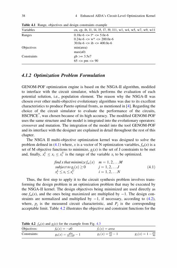
4.1.2 Optimization Problem Formulation
GENOM-POF optimization engine is based on the NSGA-II algorithm, modifiedto interface with the circuit simulator, which performs the evaluation of eachpotential solution, i.e., population element. The reason why the NSGA-II waschosen over other multi-objective evolutionary algorithms was due to its excellentcharacteristics to produce Pareto optimal fronts, as mentioned in [4]. Regarding thechoice of the circuit simulator to evaluate the performance of the circuits,HSCPICE
�, was chosen because of its high accuracy. The modified GENOM-POF
uses the same structure and the model is integrated into the evolutionary operators:crossover and mutation. The integration of the model into the tool GENOM-POFand its interface with the designer are explained in detail throughout the rest of thischapter.
The NSGA II multi-objective optimization kernel was designed to solve theproblem defined in (4.1) where, x is a vector of N optimization variables, fm(x) is aset of M objective functions to minimize, gj(x) is the set of J constraints to be metand, finally, xi
L B xi B xiU is the range of the variable xi to be optimized.
find x that minimize fm xð Þ m ¼ 1; 2; . . .Msubject to gj xð Þ� 0 j ¼ 1; 2; . . .JxL
i � xi� xUi i ¼ 1; 2; . . .N
ð4:1Þ
Thus, the first step to apply it to the circuit synthesis problem involves trans-forming the design problem in an optimization problem that may be executed bythe NSGA-II kernel. The design objectives being minimized are used directly asone fm(x), and the ones being maximized are multiplied by -1. The design con-straints are normalized and multiplied by -1, if necessary, according to (4.2),where, pj is the measured circuit characteristic, and Pj is the correspondingacceptable limit. Table 4.2 illustrates the objective and constraint functions for the
Table 4.1 Range, objectives and design constraints example
Variables cn, cp, ib, l1, l4, l5, l7, l9, l11, w1, w4, w5, w7, w9, w11
Ranges 0.18e-6 \= l* \= 5.0e-60.24e-6 \= w* \= 200.0e-630.0e-6 \= ib \= 400.0e-6
Objectives min(area)max(a0)
Constraints gb [= 3.5e765 \= pm \= 90
Table 4.2 fm(x) and gj(x) for the example from Fig. 4.3
Objectives: f0 xð Þ ¼ �a0 f1 xð Þ ¼ area
Constraints: g0 xð Þ ¼ gbw35�106 � 1 g1 xð Þ ¼ pm
65 � 1 g2 xð Þ ¼ 1� pm90
38 4 Enhanced AIDA’s Circuit-Level Optimization Kernel

differential amplifier circuit in Fig. 4.3 using the design specifications fromTable 4.1.
gi xð Þ ¼
pi�Pi
Pij j when the constraint is pi�Pi
pi when the constraint is pi� 0�pi when the constraint is pi� 0Pi�pi
Pij j when the constraint is pi�Pi
8>><
>>:ð4:2Þ
4.1.3 Outputs
Finally, the output is a set of feasible circuits with different sizing solutions, allfulfilling the constraints, giving the designer the possibility to choose the mostappropriate tradeoff among the objectives being optimized. Figure 4.4 shows aPOF obtained after the optimization of the folded cascade amplifier from Fig. 4.3,with several different sizing solutions. This set of sizing solutions allows thedesigner not only to explore various solutions within the solution space, choosingthe one that is the most suitable, but also to save a huge time in the projectexecution. The points highlighted in the POF illustrate with practical values thetradeoff between objectives. For every point in the POF, the respective values forthe dimensions of each device of the circuit are defined, and their layout can begenerated automatically with LAYGEN II. Although, only two objectives arepresented for clarity, more objectives are supported.
Area = 39,0 um2
DC gain = 54,4 dB
Area = 100,2 um2
DC gain = 64, 2 dB
Area = 781,2 um2
DC gain = 72,8 dB
Pareto Front of Sizing Solutions
25 100 225 400 425 900
-54
-56
-58
-60
-62
-64
-66
-68
-70
-72
-74
Fig. 4.4 POF obtained during the sizing task
4.1 Architecture 39

4.2 Integration of the Gradient Model in the OptimizationKernel
The integration of the Gradient Model into GENOM-POF is done by embedding it inthe crossover and mutation evolutionary operators. Each element in the population,chromosome, encodes the information of a different sizing solution, correspondingeach gene to one input variable. So, each chromosome has a fixed number of genesequal to the number of optimization variables (Fig. 4.5).
As the traditional genetic algorithms (GA), the NSGA II kernel is an evolu-tionary optimization scheme that simulates natural evolution. It operates over apopulation composed by several chromosomes, each representing a differentcandidate solution. Each chromosome differs from each other due to their differentvariables’ values. The genetic operators, crossover and mutation, are used to createnew individuals from the initial population (usually obtained randomly), the first,by combining the genetic information from the parents, and the second by intro-ducing random changes in the individual. The new individuals’ fitness is evaluatedand they are mixed with the parents and ranked. The fittest individuals are selectedas the new parents, and the others discarded. The process is repeated until theending criterion is reached (usually a fixed number of iterations). The distinguishcharacteristic of NSGA-II is that the ranking is made using Pareto dominance.Figure 4.6 shows the evolution of the population during one generation in ageneral evolutionary kernel.
The crossover operator recombines the genes in the population by generatingnew chromosomes combining two parent chromosomes to produce new offspringchromosomes. Figure 4.7 illustrates a common crossover operator. The idea is thatthe new chromosomes may correspond to better solutions than both of the parentsby taking the best characteristics from each of the parents. Crossover can becompared to reproduction in natural organisms which allows the swapping ofinformation between individuals.
The mutation operator is performed on the offspring, this operation changes thevalue of one or more genes of each chromosome, as illustrated in Fig. 4.8. Theoperator mutation increases the genetic diversity in the population, and thusincreases the capability of the algorithm to search other areas of the search space.The mutation rate is the parameter that controls the number of genes changed bythe mutation operator.
The implementation of the new genetic operators, crossover and mutation, ispresented in the following subsections.
L1W1 IBias W2 ... W11
Input variables of a circuit
Fig. 4.5 Abstractrepresentation of thechromosome in theevolutionary kernel
40 4 Enhanced AIDA’s Circuit-Level Optimization Kernel

4.2.1 Gradient Model Applied to the Crossover Operator
The first approach to integrate the Gradient Model in the optimization kernel wasby applying it to the crossover operator. The gradient rules are here used to affectthe genes of the parents as they are recombined. The gradient rules are used toselect and change the genes, which have the desired effect on the output measures.However, the mutation operator is applied over the resultant chromosomes whichcan undo the changes. Figure 4.9 exemplifies an abstract integration of theGradient Model after the crossover. The grey color represents the affected genes.
Figure 4.10 illustrates the application of a Gradient Model in the crossoveroperator, the selected gradient rule indicates that to increase the GBW output, bothW1 and IBias should be increased. The variation applied to these variables is
Crossover
Combine & Sort
Mutation
Chromosome 1
Chromosome 3
Chromosome 2
Chromosome N
. . .
N Parents
Chromosome 1
Chromosome 3
Chromosome 2
Chromosome N
. . .
N Offspring
Chromosome 1'
Chromosome 3'
Chromosome 2'
Chromosome N’
. . .
N Offspring’
Chromosome 1
Chromosome 3
Chromosome 2
Chromosome N
2N Parents & Offspring
Chromossome 1'
Chromosome 3'
Chromosome 2'
Chromosome N’
. . .
Selection
N Next Parents
. . .
Chromosome 2
Chromosome N
Chromosome 3'
Chromosome 2'
. . .
Fig. 4.6 Evolution of the population in a GA
Chromosome – Parent 1
Chromosome – Parent 2
Chromosome – Offspring 1
Chromosome – Offspring 2
Fig. 4.7 Illustration of a crossover operator
Chromosome – before Mutation Chromosome – after Mutation
Fig. 4.8 Illustration of the mutation operator
4.2 Integration of the Gradient Model in the Optimization Kernel 41

between 0 and 3 % of their value, and is defined by the Change Ratio (all changesin the illustration were done considering 3 %). The Change Ratio is one of themodel parameter, the other is the Apply Rate which controls the application or notof the model during crossover, later, in the subsection Graphical User Interface,those parameters will be explained in detail.
4.2.2 Gradient Model Applied to the Mutation Operator
Another approach to integrate the Gradient Model in the optimization kernel is tointegrate the model into the mutation operator. This approach do not fall into the
Chromosome – Parent 1
Chromosome – Parent 2
Chromosome – Offspring 1
Chromosome – Offspring 2
Gradient Model
Fig. 4.9 Crossover operator integrated with the gradient model
W1
210
W2
105
L1
0.35
L2
0.35
Ib
300
Offspring 1
W1
150
W2
115
L1
0.5
L2
0.4
Ib
200
Offspring 2
GRADIENT MODELObjective: max(GBW)Rules: W1 W2 L1 L2 Ib
GBW,(+) (+)
A0,(-)
(+)
(+) (-)
Parameters: c = 0.03
Gradient Model
W1 W2
105
L1
0.35
L2
0.35
Ib
Offspring 1
W1 W2
115
L1
0.5
L2
0.4
Ib
Offspring 2
309216.3 206154.5
Fig. 4.10 Application example of the gradient model in the crossover
42 4 Enhanced AIDA’s Circuit-Level Optimization Kernel

same problem of applying the model to the crossover operator, which can drivechromosomes for areas of optimization and then that direction be changed by theintervention of the mutation operator.
As seen before, the chromosome is represented by the vector of continuousvariables {x1,…, xn} representing the design variables. To speed up the conver-gence of the algorithm, the knowledge extracted from the gradient model is used tomake the mutation operator more efficient. The reference mutation operator inGENOM-POF uses the continuous valued operator introduced by Deb and Goyalin [7]. In this mutation operator, di is the mutation perturbation applied and isdefined as di ¼ xM
i � xi
� �= XMax
i � XMini
� �, where xM
i and xi are the mutated andoriginal values, respectively. Moreover, di is a random variable, with values in theinterval of -1 to 1, and probability density function given by (4.3), where, g is aparameter used to control the distribution’s spread. Figure 4.11 shows the p.d.f. forvarious values of g.
PðdÞ ¼ 0:5� ðgþ 1Þ � ð1� dj jÞg ð4:3Þ
A factor of disturbance �d of d can be obtained from a uniform random number
u 2 0; 1½ � using (4.3), which is obtained from (4.4) by solvingR d�1 PðdÞ ¼ u.
d ¼ ð2uÞ2
gþ2 � 1; if u\0:5
1� 2 1� uð Þ½ �2
gþ2; if u� 0:5
(
ð4:4Þ
Then, the mutated value, xMi , is given by xM
i ¼ xi þ d XMaxi � XMin
i
� �. The gra-
dient rules obtained during the generation of the gradient model are then applied.The application of the rules follows (4.5), where xG
i is the variable value after theapplication of the rule, c Siið Þ is a function of the gradient symbol defined in (4.6),and u 2 0; c½ � is a uniformly distributed random number between 0 and c, theChange Rate model parameter.
xGi ¼ 1þ l:c Siið Þð Þ xM
i ð4:5Þ
η = 0η = 1η = 5
δ
P(δ)
-1 10
1
0.5
3Fig. 4.11 Probabilitydistribution for creating amutated value [7]
4.2 Integration of the Gradient Model in the Optimization Kernel 43

c Siið Þ ¼þ1 when Sii ¼ ðþÞ�1 when Sii ¼ ð�Þ
�
ð4:6Þ
The application of the gradient rules is dependent on the existence of a suitablerule for the optimization targets, i.e., it is irrelevant to have a rule to decrease thegain, if the optimization target is to increase it. The rules are selected by searchingif there is a rule that causes the desired effect on each optimization objective. Ifthis rule is found, then the variables with larger contributions are affected asdescribed before. Figure 4.12 shows an example of applying a gradient rule.
Once again, in the example the Gradient Model indicates to increase the valuesof W1 and IBias, and with a maximum percentage of changing the values of 3 %.After the model application the chromosome may have incorporated the knowl-edge needed to achieve faster the optimal solution. With the introduction of circuitknowledge through the gradient it is expectable to reach sub-optimal solutionsfaster than GENOM-POF without model, or even to reach optimal solutions thatGENOM-POF cannot reach alone. Figure 4.13 presents an example of the muta-tion operator integrated with Gradient Model.
W1
216.3
W2
105
L1
0.35
L2
0.35
Ib
309
Individual: after gradient model
W1
210
W2
105
L1
0.35
L2
0.35
Ib
300
Individual: after mutation
Gradient Model
GRADIENT MODEL
W1
(+)GBW,(+)
W2 L1 L2 Ib
(+)
A0,(-) (+) (-)
Rules:
Parameters: c = 0.03
Objective: max(GBW)
Fig. 4.12 Example of application of the gradient model in the mutation
W1
W2
W3
Increase W3 (3%)
Increase W3 (1%)
Gradient Model: Increase W3
(0% - 3%)
Resulting point
Mutation decrease W2
Resulting point
Mutation increase W1
Fig. 4.13 Solutions searchspace for mutation integratedwith gradient model
44 4 Enhanced AIDA’s Circuit-Level Optimization Kernel

4.3 Graphical User Interface (GUI)
The AIDA environment integrated with the Gradient Model, framework and GUIare implemented in JavaTM 1.6. This GUI provides a simple and fast way for thedesigner to set the values of constraints and the range of the optimization variables,also through the GUI the designer can set the type of optimization to be made onobjectives (maximize or minimize), and monitor the results at any stage of theevolutionary generation.
Figure 4.14 presents the overview of the AIDA’s GUI. From this overview isalready possible to identify in the upper left the schematic of the circuit in use.Beneath the schematic are the options available to the user for controlling thecircuit, model and algorithm, which will be presented in detail below. In the right,on top the estimated layout and on bottom the details, of each of the solutions inthe POF listed in the center, are presented.
Figure 4.15 shows possible objectives (DC Gain and area) for a design, how-ever, these can be chosen by the designer through the GUI since they are defined inthe netlist. Also, using the GUI the designer can define the type of objectiveintended to maximize or minimize.
In Fig. 4.16 it is possible to see the constraints of design and their limits. Thelimits and type of the constraints ([= or \=) can be easily changed. Also, theoutput being limited can be chosen from any of the available performancemeasures.
Fig. 4.14 AIDA GUI: overview
4.3 Graphical User Interface (GUI) 45

Fig. 4.15 AIDA GUI: objectives
Fig. 4.16 AIDA GUI: constraints
46 4 Enhanced AIDA’s Circuit-Level Optimization Kernel

These two panels allow the designer to make several studies for the samecircuit, by changing the values of the objectives and their constraints. However,the designer can also change the search space for the optimization problem bychanging the range of the input variables. Figure 4.17 shows the several optimi-zation variables considered in optimization of this circuit, and their respectiveminimum and maximum range. The designer can change these ranges values to hisown desire by introducing those values in the GUI. Changing the ranges of the
Fig. 4.17 AIDA GUI: ranges of the input variables
4.3 Graphical User Interface (GUI) 47

design variables changes the search space, it reduces when the ranges aredecreased and expands as the ranges increase. The point to keep in mind is thatwith narrower search space, the algorithm converges faster to the optimal solu-tions, while with a larger search space the same algorithm will have more difficultyin finding the optimal solutions.
Other options like the type of strategy to use or the possibility to use or not theGradient Model are included in GUI, also the designer can setup the parameters ofthe NSGA-II and the Gradient Model. Figure 4.18 shows the type of strategy to be
Fig. 4.18 AIDA GUI: gradient model and optimization options
48 4 Enhanced AIDA’s Circuit-Level Optimization Kernel

adopted for the optimization problem, GENOM-POF supports both typical andcorner optimization, however, in this work only the typical strategy is considered.
The following settings, in Fig. 4.18, are: the use or not of the Gradient Model orthe Random Model; the model application parameters, respectively, Apply Rate,which is the frequency/percentage of use of the model chosen in the optimizer, andChange Ratio, which is the maximum percentage of change of the value of avariable. The Random Model will be presented in the next chapter, together withthe results, and is used as reference for comparison with the Gradient Model; thelast options are the NSGA-II parameters, the mutation rate controls the percentageof genes that are mutated in each generation and influences the diversity of thepopulation, the population size is the number of individuals (chromosomes) in apopulation participating in the evolutionary process, and the crossover rate definesthe frequency/percentage of the crossover operation, and, finally, the number ofgenerations, which corresponds to the number of execution cycles of the algorithm.
4.4 Conclusions
This chapter introduced the architecture of the AIDA environment for the auto-matic synthesis of analog integrated circuits. The more specific architecture ofGENOM-POF was also presented, which is the tool for circuit sizing optimization.All the specifications like inputs, structure of the optimization kernel, designstrategies, and the outputs were explained. The integration of the model into theoptimization kernel was detailed described. The focus was kept on the evolu-tionary operators since the Gradient Model is applied through the crossover ormutation operator. Finally, this chapter also introduced the AIDA’s GUI.
References
1. N. Lourenço, N. Horta, GENOM-POF: multi-objective evolutionary synthesis of analog ICswith corners validation, in Proceedings of the fourteenth international conference on Geneticand evolutionary computation conference (GECCO ‘12), pp. 1119–1126. July 2012.doi:10.1145/2330163.2330318
2. R. Martins, N. Lourenco, S. Rodrigues, J. Guilherme, N. Horta, AIDA: Automated analog ICdesign flow from circuit level to layout, in Synthesis, Modeling, Analysis and SimulationMethods and Applications to Circuit Design (SMACD), International Conference on,pp. 29–32, Sept 2012. doi:10.1109/SMACD.2012.6339409
3. R. Martins, N. Lourenço, N. Horta, Generating Analog IC Layouts with LAYGEN II,SpringerBriefs in Applied Sciences and Technology–Computational Intelligence, (Springer,New York, 2013)
4. R. Martins, N. Lourenço, N. Horta, LAYGEN II-automatic layout generation of analogintegrated circuits, for publication in IEEE Transactions on Computer-Aided Design ofIntegrated Circuits and Systems, doi: 10.1109/TCAD.2013.2269050
4.3 Graphical User Interface (GUI) 49

5. R. Martins, N. Lourenço, N. Horta, Routing analog ICs using a multi-objective multi-constraint evolutionary approach. Analog Integr. Circuits Signal Process. 1–13 (2013).doi:10.1007/s10470-013-0088-9
6. K. Deb, A. Pratap, S. Agarwal, T. Meyarivan, A fast and elitist multiobjective geneticalgorithm: NSGA-II. IEEE Trans. Evol. Comput. 6(2), 182–197 (2002)
7. K. Deb, M. Goyal, A combined genetic adaptive search (GeneAS) for engineering design.Comput. Sci. Inform. 26(4), 30–45 (1996)
50 4 Enhanced AIDA’s Circuit-Level Optimization Kernel

Chapter 5Results
Abstract This chapter illustrates the application of the proposed methodology topractical examples. The framework of the proposed methodology for the automaticgeneration of analog integrated circuits (IC) layout has been coded in JAVA andwas executed, for the presented examples, on an Intel� CoreTM 2 Quad CPU2.4 GHz with 6 GB of RAM.
Keywords Analog IC design � Circuit-level sizing � Evolutionary computation �Gradient model
5.1 POFs Analysis
In this study, two objectives are considered to illustrate the multi-objective natureof the proposed optimization approach, which also facilitates a clear graphicalrepresentation of the Pareto optimal fronts (POF). In order to compare GENOM-POF [1] with the integrated solution GENOM-POFGM (GENOM-POF ? Gradi-ent Model) the following POF performance indicators are defined:
• Non-dominated area of the POF;• Number of points in the POF;• Standard deviation of points on the f1(x) axis of the POF;• Standard deviation of points on the f2(x) axis of the POF.
Before entering into the details of the performance indicators, it is important tograsp the meaning of Pareto dominance, illustrated in Fig. 5.1. The definition ofdominance states that a solution xi dominates a solution xj, if both the followingconditions are true:
F. A. E. Rocha et al., Electronic Design Automation of Analog ICs Combining Gradient Modelswith Multi-Objective Evolutionary Algorithms, SpringerBriefs in Computational Intelligence,DOI: 10.1007/978-3-319-02189-8_5, � The Author(s) 2014
51

• The solution xi is not worse than xj in any objectives;• The solution xi is strictly better than xj in at least one objective.
If any of the above conditions is violated the solution xi does not dominate thesolution x3. For a given set of solutions, all possible pairwise comparison should beperformed in order to find which of those are the non-dominated solutions formingthe Pareto front.
Either the dominated or the non-dominated area of the POF are extremelyrelevant indicators to make a quantitative comparison among POFs and arecomputed as follow:
• The axis are normalized to be between 0 and 1;• The dominated area, illustrated in Fig. 5.2 by A, is calculated by the sum of
trapezoidal areas defined by successive POF elements as described by expres-sion (5.1):
A ¼X 1� að Þ þ 1� bð Þ
2
� �
� h ð5:1Þ
• The non-dominated area, illustrated in Fig. 5.2 as area B, was defined as beingB = 1-A. Thus, the smaller the non-dominated area, the better is the generatedPOF.
f1(x)
f2(x)
x2
x1x3
Fig. 5.1 Pareto dominance:x2 is dominated by x1 while x1
and x3 are not dominated,assuming both f1 and f2 arebeing minimized
Area
h
A
1
1a b
f1(x )
B
f2 (x )
Fig. 5.2 Dominated andnon-dominated areas
52 5 Results

5.2 Circuit Under Test: Single-Ended Folded CascodeAmplifier
The single-ended folded cascade amplifier, which schematic and test bench arepresented in Fig. 5.3, is here used to compare GENOM-POF with GENOM-POFGM. In all the studies, the l UMC (United Microelectronics CorporationGroup) complementary metal–oxide–semiconductor (CMOS) technology wasconsidered. Two different studies were performed, the first considering 15 inputvariables (15th dimensional search space), which corresponds to a large solutionsearch space, and the second reducing the input variables to 12 (12th dimensional).
ip
In
Vbp
Vdd
Vss
Ib
Ibp=1.1Ib
Vac
VipVbpc
Vbnc
Vb Vss Vbnc
out
Vbpc Vdd
W=W5L=L5M=M5
W=W5L=L5M=M5
W=W7L=L7M=M7
W=W7L=L7M=M7
W=W9L=L9M=M9
W=W9L=L9M=M9
M1
Vdd
Vbp
Vbpc
inip
Vss
out
Vbnc
vb
M2
M4 M11 M12
M9 M10
M7 M8
M5 M6
W=W1L=L1M=M1
W=W1L=L1M=M1
W=W4L=L4M=M4
W=W11L=L11M=M11
W=W11L=L11M=M11
Amplifier
(b)
(a)Fig. 5.3 Schematic andtestbench of the single-endedfolded cascode amplifier
5.2 Circuit Under Test: Single-Ended Folded Cascode Amplifier 53

5.3 Case Study I: 15 Input Variables
The first case study was performed considering 15 input/optimization variables, 2objectives and the performance and functional constraints, as defined in Table 5.1.The optimization variables include the W’s and L’s of all transistors, the cascodebias tensions, represented by vbcp and vbcn respectively, and the bias current. Thisoptimization task is executed by GENOM-POF and by GENOM-POFGM for thevery same conditions.
5.3.1 GENOM-POF
Before proceeding with the evaluation of GENOM-POFGM, a brief study to tunethe optimal mutation rate was performed. The crossover rate, the number of ele-ments in the population and the number of generations were fixed to the values90 %, 128 and 2,000, respectively. As a starting point, GENOM-POF was exe-cuted with the mutation rate of 3 %. Others tests were made for a mutation rate of5, 15, 30 and 45 %. The best mutation rate found was 30 %, Fig. 5.4 shows theevolution of the POF in one optimization run using the mutation rate of 3 %, andFig. 5.5 shows the evolution of the POF with the mutation rate of 30 %. Observingboth plots, it can be noticed that the POF obtained with a 3 % mutation rate ismore smooth, however the POF obtained with the mutation rate of 30 % clearlydominates the one obtained with the 3 % mutation rate, for the same number of
Table 5.1 Range, objectivesand constraints
Variables vbcn, vbcp, l1, l4, l5, l7, l9, l11,ib, w1, w4, w5, w7, w9, w11
Ranges 0.18 lm \= l* \= 5.0 lm0.24 lm \= w* \= 200.0 lm-400 mV \= vbcn \= 0.0 V0.0 V \= vbcp \= 400 mV30.0 lA \= ib \= 400.0 lA
Objectives Min(area)Max(a0)
Constraints gb [= 12 MHzdc_gain [= 80 dB558\= pm \= 908sr [= 10 V/lsOverdrive_m(*) [= 30 mVDelta_m(*) [= 1.2osp [= 300 mVosn \= -300 mV(*) the constraints apply to:M1, M4, M5, M7, M9 and M11
54 5 Results

generations. This difference is due to the fact that smaller mutation rates lead toearly convergence issues; moreover, the mutation operator used, unlike otherapproaches where the new genes are set as random value within the allowed rangeas the new genes, generates new genes that are in average close the original values,thus the better performance when using a higher mutation rate.
With the mutation rate tuned, an exhaustive optimization with 60,000 genera-tions was performed; the obtained POF is shown in Fig. 5.6. Both POFs provide areference to the evaluation of the performance of GENOM-POFGM.
area [m2 ]
dc g
ain
[dB
]
Fig. 5.4 GENOM-POF with mutation rate: 3 % and for 2,000 generations
area [m 2 ]
dc g
ain
[dB
]
Fig. 5.5 GENOM-POF with mutation rate: 30 % and for 2,000 generations
5.3 Case Study I: 15 Input Variables 55

5.3.2 GENOM-POFGM
For this example a Gradient Model was generated considering a Design ofExperiments (DOE) matrix with base two (B = 2) and the contribution of oneoptimization variable (N = 1). The resulted Gradient Model for both objectives isshown in Tables 5.2 and 5.3.
The generated Gradient Model shows a positive gradient for both objectives,i.e., for the maximization of the DC gain the model tells us to increase the value ofthe variable L9, and for the minimization of area the model indicates to thealgorithm to decrease the value of W11. The generated model for this exampletook less than 5 min to be generated and the model can be reused for the samecircuit and optimization variables but with different values of constraints. Theusage of the Gradient Model is tuned using the model parameters: Apply Rate andChange Ratio, as detailed in Chap. 4. To tune these parameters several tests wereperformed and the values of 50 and 3 % were found to be the respective best.
area [m 2 ]
dc g
ain
[dB
]
Fig. 5.6 GENOM-POF for 60,000 generations
Table 5.2 Gradientgenerated for DC gain
DC gain
L9 Gradient (-) (-)L9 Gradient (+) (+)
Table 5.3 Gradientgenerated for area
Area
W11 Gradient (-) (-)W11 Gradient (+) (+)
56 5 Results

GENOM-POFGM was then used to optimize the same circuit in the sameconditions used for GENOM-POF (mutation rate of 30 %, crossover rate of 90 %and population size of 128 and 2,000 generation). The POF obtained is shown inFig. 5.7.
Figure 5.8 shows the POFs obtained from 2,000, 4,000 and 60,000 optimizationgenerations in GENOM-POF, and, superimposed, the POF obtained from 2,000optimization generations in GENOM-POFGM. The POF obtained with GENOM-POFGM, with only 2,000 generations, clearly dominates the ones obtained withGENOM-POF for 2,000 and 4,000 generations. Even the POF obtained after anexhaustive optimization with 60,000 generations, thought generically better, doesnot dominate completely the POF obtained with GENOM-POFGM, not reachingthe maximum value for DC Gain reached by GENOM-POFGM. These results
area [m 2 ]
dc g
ain
[dB
]
Fig. 5.7 GENOM-POFGM (apply rate = 50 % and change ratio = 3 %) for 2,000 generations
area [m 2 ]
dc g
ain
[dB
]
Fig. 5.8 GENOM-POF (60,000, 4,000, and 2,000 gen.) versus GENOM-POFGM (2,000 gen.)
5.3 Case Study I: 15 Input Variables 57

show the effectiveness of the knowledge captures by the Gradient Model toachieve better solutions faster than the GENOM-POF for the same number ofgenerations.
The 2,000 generations were executed in approximately 30 min, for the 4,000generations the time doubles, and for the 60,000 generations the optimizationprocess takes approximately 15 h. GENOM-POFGM for 2,000 generations showscompetitive results in comparison with GENOM-POF for 60,000 generations inapproximately less 14 h and 30 min. To confirm that this is not an isolated case, 20executions with different seeds were performed. The results are shown in Fig. 5.9,where it can be seen that the inclusion of the gradient model consistently lead tobetter solutions.
5.3.3 Random Model
Additionally, and to show that selecting the variables with higher contribution anddetermining their correct gradient assignment is crucial to improve the optimi-zation kernel performance, a Random Model was created to validate the usefulnessof the Gradient Model. The Random Model consists of choosing N randomvariables and affecting them with a random gradient, the pseudo-code is presentedin Algorithm 5.1 where the parameters N, Apply Rate and Change Ratio have thesame meaning as in the Gradient Model.
The random model was used together with GENOM-POF to optimize thefolded cascade amplifier 20 times as in the previous examples. The obtained POFis shown in Fig. 5.10, where it can be seen that by embedding circuit knowledge inGENOM-POF there are effective benefits to the sizing and optimization task.
area [m 2 ]
dc g
ain
[dB
]
Fig. 5.9 20 different initial populations for comparison between GENOM-POF and gradientmodel
58 5 Results

5.3.4 Comparison of Different Optimization/SizingApproaches
To quantify the graphical analysis described this far, Tables 5.4, 5.5 and 5.6summarize for each run the following numerical and statistical indicators:
• Low Area: Finding the minimum circuit area is one of the objectives of thisdesign problem, so the lowest area reached is an indicator that a designer wouldtake into consideration. This indicator is represented by the coordinates in theobjective space (area, dc gain) of the solution with the lowest area.
• Max DC Gain: Finding the maximum DC gain is another objective of this designproblem, and is also used an indicators represented by the coordinates in theobjective space (area, dc gain) of the solutions with the greatest DC gain.
area [m 2 ]
dc g
ain
[dB
]
Fig. 5.10 Random model for 20 different initial populations
5.3 Case Study I: 15 Input Variables 59

• Number of points in POF: This parameter counts the number of solutions whichcompose the last generated POF.
• Area B: Represents the non-dominated area for both objectives.• Standard deviation of area and dc gain and their product: these parameters are
the standard deviations of the difference between objective values of two con-secutive solutions in the ordered POF; they aim to analyze the spread of solu-tions for each objective and for both objectives.
The results in Tables 5.4, 5.5, 5.6 show that GENOM-POF reaches a maximumDC Gain around 86.81 dB for the seed 12 and a minimum area around 1676 lm2
Table 5.4 POFs (20 different seeds) analysis for GENOM-POF
Population: 128 Mutation: 30 % Crossover: 90 % Nr. of Generations 2,000
Run ID Low area[lm2, dB]
Max DCgain[lm2, dB]
#Points
Area:1 - A= B
,area ,dc
gain
,area 9 ,dc gain
0 (2008,80.21)
(5004,85.19)
63 0.435 1.523 1.278 1.947
2 (1676,80.67)
(4528,85.36)
48 0.390 1.383 1.185 1.640
… … … … … … … …12 (1736,
80.56)(4204,
86.81)47 0.231 1.302 0.837 1.091
19 (2304,80.76)
(4963,84.48)
46 0.511 1.093 1.118 1.223
Mean 51.55 0.426 1.549 1.188 1.842Standard
deviation8.438 0.085 0.479 0.163 0.621
Table 5.5 POFs (20 different seeds) analysis for gradient model
Population: 128 Mutation: 30 % Crossover: 90 % Nr. of Generations 2,000
Run ID Low area[lm2, dB]
Max DCgain[lm2, dB]
#Points
Area:1 - A= B
,area ,dc
gain
,area 9 ,dc gain
0 (1544,80.10)
(5167,87.85)
85 0.134 1.346 1.172 1.578
3 (1426,80.18)
(6881,87.20)
87 0.197 1.732 1.168 2.024
… … … … … … … …11 (1596,
80.05)(6493,
88.07)95 0.117 1.197 1.159 1.388
19 (2257,80.26)
(5647,86.30)
66 0.348 1.220 1.023 1.249
Mean 81.7 0.200 1.527 1.162 1.784Standard
deviation16.799 0.081 0.496 0.116 0.619
60 5 Results

in the seed two. GENOM-POFGM reaches the maximum DC Gain of 88.07 dB atseed 11 and the minimum area 1430 lm2 in the seed three. Finally, the GENOM-POF plus the Random Model achieves the maximum of 84.86 dB at seed 10 andthe minimum area 1846 lm2 in the seed seven.
However, all these maximum and minimum values are achieved in differentseeds. So, the mean of the non-dominated areas becomes a relevant value todifferent approaches. By observing these tables, the Gradient Model presents verygood results in terms of non-dominated area by having the lowest areas.
Finally, the observation of the non-dominated area, the number of points in thePOF and the standard deviations leads to the conclusion that GENOM-POFGMperforms significant better than the other tested approaches. Table 5.7 summarizesall the comparisons between the gradient and random models and the referenceGENOM-POF implementation.
5.4 Case Study II: 12 Input Variables
Using the same circuit as before, but now with a number of optimization variablesreduced to 12, by removing the biasing variables ib, vbcn and vbcp, while keepingthe objectives and constraints.
Table 5.6 POFs (20 different seeds) analysis for random model
Population: 128 Mutation: 30 % Crossover: 90 % Nr. of Generations 2,000
Run ID Low area[lm2, dB]
Max DCgain[lm2, dB]
#Points
Area:1 - A= B
,area ,dc
gain
,area 9 ,dc gain
0 (2731,80.18)
(7013,84.29)
98 0.482 1.604 1.093 1.755
7 (1846,80.11)
(4031,84.42)
117 0.407 1.185 1.388 1.645
… … … … … … … …10 (2102,
80.33)(11480,
84.86)91 0.416 2.639 1.196 3.1589
19 (2.359,80.51)
(8147,84.20)
72 0.467 3.592 1.260 4.529
Mean 93.8 0.455 2.444 1.281 3.156Standard
deviation16.516 0.029 0.873 0.155 1.253
5.3 Case Study I: 15 Input Variables 61

5.4.1 GENOM-POF
Figure 5.11 illustrates the GENOM-POF optimization runs with the mutation rateof 30 %, crossover rate of 90 %, population size of 128, the number of generationsof 2,000 for 20 different runs.
It is clear that results are now below the ones in the previous example (shown inFig. 5.6). This is due to the reduction in the number of optimization variables,especially the fixed biasing of the circuit. The previous example showed a max-imum DC Gain around 85 dB and a minimum area around 2000 lm2 however, inthis example the maximum DC Gain is around the 84 dB and the minimum area isaround 3000 lm2.
Table 5.7 Comparison between the gradient and random models and GENOM-POF
Non-dominatedarea
Nr. points POF ,area ,dc gain ,area 9 ,dc gain
Gradientmodel
Better thanGENOM-POF
Better thanGENOM-POF
Similar toGENOM-POF
Similar toGENOM-POF
Similar toGENOM-POF
Randommodel
Worse thanGENOM-POF
Better thanGENOM-POF
Worse thanGENOM-POF
Similar toGENOM-POF
Worse thanGENOM-POF
area [m 2 ]
dc g
ain
[dB
]
Fig. 5.11 GENOM-POF optimization for case study II
62 5 Results

5.4.2 GENOM-POFGM
The Gradient Model for this example was generated like the one generated in theprevious example, and is shown in Tables 5.8 and 5.9.
Figure 5.12 shows the 20 POFs obtained for 20 different optimization runs withGENOM-POFGM. Like the previous example the Apply Rate is 50 % and theChange Ratio is 3 %.
Like the result obtained with GENOM-POF, this result, in comparison with theresults shown in Fig. 5.8, presents a real deterioration of the solutions. For thisoptimization the maximum DC Gain obtained is around the 84 dB while beforewas around 88 dB. Also for the area measure the solutions found are worse,around the 3000 lm2 nm while before was around 2000 lm2.
The results for both GENOM-POF and GENOM-POFGM are worse in this casethan in the case with 15 optimization variables. This deterioration is explainedwith the fixed variables ib, vbcn and vbcp, which limits the range of operation ofthe circuit.
5.4.3 Comparison of Different Optimization/SizingApproaches
The first way to compare GENOM-POF and GENOM-POFGM is performed byanalyzing their POFs. Figure 5.13 shows the overlay of both POFs in the sameplot. It does not show significant improvements, as both results seem very similar.
Besides the visual analysis of the POFs does not allow any conclusion about theimprovement or not with the Gradient Model, the statistical study does confirm thecontribution of the proposed approach. Tables 5.10 and 5.11 show the analysesperformed for GENOM-POF and GENOM-POFGM respectively. As observedbefore in the POFs, Tables 5.10 and 5.11 do not show significant improvements bythe integration of the Gradient Model. The lowest value of area of 2607 llm2
reached by GENOM-POF and 2577 lm2 reached by GENOM-POFGM, are, inpractical terms, the same. The same happens to the maximum DC Gain, GENOM-
Table 5.8 Gradient rulesgenerated for DC gain
DC gain
L11 Gradient (-) (-)L11 Gradient (+) (+)
Table 5.9 Gradient rulesgenerated for area
Area
W5 Gradient (-) (-)W5 Gradient (+) (+)
5.4 Case Study II: 12 Input Variables 63

POF presents the maximum of 84.1 dB while GENOM-POFGM achieves themaximum DC Gain of 84.41 dB.
However, a careful analysis of the non-dominated area (defined as area B) showthat the non-dominated area is generically lower for the case of GENOM-POFGM.To further study this phenomenon, for each seed, the POFs from the generation500 to the generation 2,000 were analyzed showing that GENOM-POFGM hadconsistently less non-dominated area, which means that reaches better solutionsfaster than GENOM-POF. The summary of these results is presented inTable 5.12.
area [m 2 ]
dc g
ain
[dB
]
Fig. 5.12 GENOM-POFGM optimization for case study II
area [m 2 ]
dc g
ain
[dB
]
Fig. 5.13 Comparison between GENOM-POF and GENOM-POFGM
64 5 Results

Table 5.10 POFs (20 different seeds) analyses for GENOM-POF
Population: 128 Mutation: 30 % Crossover: 90 % Nr. of Generations 2,000
Run ID Low area[lm2, dB]
Max DCgain[lm2, dB]
#Points
Area:1 - A= B
,area ,dc
gain
,area 9 ,dc gain
0 (2799,80.00)
(8345,84.10)
129 0.287 1.297 0.638 0.828
… … … … … … … …11 (2607,
80.02)(7501,
83.92)130 0.293 1.593 0.605 0.965
19 (2646,80.04)
(6590,83.56)
128 0.333 1.640 0.658 1.079
Mean 128.75 0.329 1.467 0.659 0.970Standard
deviation1.2085 0.046 0.374 0.054 0.264
Table 5.11 POFs (20 different seeds) analyses for gradient model
Population: 128 Mutation: 30 % Crossover: 90 % Nr. of Generations 2,000
Run ID Low Area[lm2, dB]
Max DCGain[lm2, dB]
#Points
Area:1 - A= B
,area ,dc
gain
,area 9 ,dc gain
0 (2647,80.01)
(7238,83.77)
128 0.308 1.789 0.729 1.305
2 (2577,80.02)
(8784,84.41)
128 0.241 1.583 0.533 0.843
… … … … … … … …19 (2755,
80.25)(8049,
84.23)128 0.262 1.718 0.693 1.191
Mean 128.4 0.274 1.629 0.675 1.106Standard
deviation0.882 0.029 0.206 0.093 0.239
Table 5.12 Analyze of non-dominated area
Nr. of time that have less non-dominated area thenGENOM-POF
Percentage that have less non-dominated area thenGENOM-POF
Total number ofPOFs analyzed
Gradientmodel
270 84.64 % 319
5.4 Case Study II: 12 Input Variables 65

5.5 Conclusions
In this chapter the proposed approach was tested with different scenarios showingits effective contribution to improve results and accelerate convergence.
First, an example considering an optimization for 15 input variables was per-formed, which corresponds to a wide search space of solutions. For this examplethe performance of GENOM-POF, GENOM-POFGM and GENOM-POF inte-grated with Random Model was analyzed. The conclusions were quite clear andproved that GENOM-POFGM presents significant improvements for the sizing/optimization task. This study also shows that GENOM-POFGM reaches a bettersolution for the maximization of DC Gain. In a second example, the number ofvariables to be optimized was reduced to 12, and the reduction in the problemcomplexity also lead to less significant improvement with GENOM-POFGM. InTable 5.13 some closing remarks are presented.
Reference
1. N. Lourenço, N. Horta, in GENOM-POF: Multi-Objective Evolutionary Synthesis of AnalogICs with Corners Validation. GECCO’ 12: Proceedings of the 14th International Conferenceon Genetic and Evolutionary Computation Conference, July 2012, pp. 1119–1126
Table 5.13 Comparison between GENOM-POF and GENOM-POFGM
Advantages Disadvantages
GENOM-POF
Good application to a unknown circuitGood ability to adapt to any problemExpandable to n dimensional space
The execution time can be high, becausethe entire analysis requires manyevaluations of the outputs during theexecution of internal GA
The user has no control over theoptimization
GENOM-POFGM
Time model generation greatly reduced(even negligible), for both simple andcomplex circuits
Simple and functional implementationPossibility for the designer to change the
gradient of the variables, the rate ofapplication of the model and the rateof change the value of the variables
Offers robustness for problems wherethe search space is large
66 5 Results

Chapter 6Conclusions and Future Work
Abstract The proposed methodology for the enhancement of a state-of-the-artcircuit-level synthesis approach, GENOM-POF [1], by incorporating a gradientmodel into a multi-objective multi-constraint optimization kernel was proved bythe implementation of a tool, GENOM-POFGM (GENOM-POF ? GradientModel), which is able to generate robust circuit sizing solutions. This chapterpresents the closing remarks, and the future directions for the continuous devel-opment of GENOM-POFGM.
Keywords Analog IC design �Circuit-level sizing �Electronic design automation �Computer-aided-design
6.1 Conclusions
The presented methodology corresponds to an innovative integrated circuit (IC)design automation approach by embedding a simple but effective designknowledge model, Gradient Model, into the evolutionary optimization kernel of astate-of-the-art analog circuit-level sizing tool. The new technique proved to becapable to accelerate and reduce the execution time of the circuit-level optimizerGENOM-POF. This integration of the Gradient Model with GENOM-POFenhances the optimizer efficiency, forwarding the data to the desired objectivesand causing a significant reduction in the number of electrical simulations, i.e.,required evaluations.
The model generation was performed using a Design of Experiments samplingtechnique, with two alternative strategies, Full Factorial Design and FractionalFactorial Design, and both showed no contradictions in their statistical analysis.
The Gradient Model has as main goal the description of a set of simple gradientrules, providing the designer with a direct analysis showing the contribution of theinput variables to the desired objectives and/or performance measures. The modelalso offers a set of parameters which the user can explore and vary to adapt to the
F. A. E. Rocha et al., Electronic Design Automation of Analog ICs Combining Gradient Modelswith Multi-Objective Evolutionary Algorithms, SpringerBriefs in Computational Intelligence,DOI: 10.1007/978-3-319-02189-8_6, � The Author(s) 2014
67

proposed problem, using the graphical user interface. This optimizer represents atotally automated alternative to the traditional optimization techniques, where theexecution time is usually extremely high.
The Gradient Model integrated with the mutation operator of the geneticalgorithm proved to be useful to bias the search direction into the most promisingdirection. The model application has been proved through the presentation of acomplex case study. This case study was divided in two different problems, wherein the first exists a large solution space and in the second the solutions space isreduced. These two examples validated the fact that Gradient Model integrated inGENOM-POF presents better solutions for large solutions space; and also, theseexamples proved that even for the worst case, small solution space, the GradientModel does not worsened the results of GENOM-POF and still get smallimprovements over the GENOM-POF results.
Finally, the proposed objectives for this work were achieved and a new opti-mizer was created.
6.2 Future Work
In analog IC design automation, there is still a long way to end in this domain; theimprovement on productivity of analog design is a demand of economic market.Based on this work and its large application on analog design, there are somesuggestions for future research which may improve even more its efficiency.
The first suggestion is the application of Gradient Model for the Corners val-idation. The second suggestion is to improve the accuracy of the model by per-forming an extra sample step of the circuit after reaching the first Pareto optimalfront (POF). Several other opportunities can easily be pointed out for future workshowing the large potential of the presented approach.
The integration of the model in the GENOM-POF optimization kernel can alsobe performed in alternative ways. An alternative is its application to only oneobjective variable, other alternative approach is an application of the GradientModel that is not always the same. Figure 6.1 shows an approach where the modelis applied to just one of the objectives half of the time (25 % each of the objec-tives), while the other half of the time it is applied to all the objectives. Theexpected result with this alternative approach is to accelerate the optimizationprocess by the application of the model to all the optimization objectives, and atthe same time to maximize/minimize even more the objectives by the singleapplication of the model to a specific objective.
68 6 Conclusions and Future Work

Reference
1. N. Lourenço, N. Horta, in GENOM-POF: Multi-Objective Evolutionary Synthesis of AnalogICs with Corners Validation. GECCO’ 12: Proceedings of the 14th International Conferenceon Genetic and Evolutionary Computation Conference, July 2012, pp. 1119–1126
50% of application of the Gradient Model to all
Objectives
25% of application of the Gradient Model to Area
25% of application of the Gradient Model to Gain
Fig. 6.1 Alternative approach to apply the gradient model
Reference 69
Download more eBooks here: http://avaxhm.com/blogs/ChrisRedfield