fpga based pwm techniques for controlling inverter · fpga based pwm techniques for controlling...
TRANSCRIPT
[1]
FPGA based PWM techniques for controlling
Inverter
A thesis submitted in partial fulfillment of the requirements for the degree
of
Bachelor of Technology
in
Electronics and Instrumentation Engineering
by
Suryakant Behera
Roll No. 10607011
Under the guidance of
Prof. Kamalakanta Mahapatra
[2]
National Institute of Technology Rourkela CERTIFICATE
This is to certify that the thesis entitled, “FPGA based PWM techniques for
controlling Inverter” submitted by SURYAKANT BEHERA (Roll No.-
10607011) in partial fulfilment of the requirements for the degree of Bachelor of
Technology in Electronics & Instrumentation Engineering, Session 2006-2010, in
the Department of Electronics and Communication Engineering, National Institute
of Technology, Rourkela is an authentic work carried out by him under my
supervision and guidance.
To the best of my knowledge, the matter embodied in the thesis has not been
submitted to any other University / Institute for the award of any Degree.
Date: Prof. K.K. Mahapatra
Project Guide
Dept. of Electronics & Communication Engineering
National Institute of Technology Rourkela – 769008

[3]
ACKNOWLEDGEMENT
I wish to express my deep sense of gratitude and indebtedness to Prof. Kamalakanta
Mahapatra, Department of Electronics and Communication Engineering, N.I.T. Rourkela for
introducing the present topic and for his inspiring guidance, valuable suggestions and support
throughout this project work.
I am thankful to all my Professors and Lecturers and members of the department for their
generous help in various ways for the completion of the thesis work.
I also want to thank Mr.Sushant Kumar Pattnaik, M.Tech(Res), and Mr.Ayas Kanta Swain,
M.Tech(Res) of NIT ROURKELA for helping me out during the execution of my project.
I would love to thank my family members for encouraging me at every stage of this project
work. Last but not least, my sincere thanks to all my friends who have patiently extended all
sorts of help for accomplishing this undertaking.
Suryakant Behera
Roll No: 10607011
[4]
Contents
Abstract………………………………………………………………………………………………………………………………….7
Chapter 1 Introduction………………………………………………………………………...8
1.1 Introduction………………………………………………………………………9
1.2 Advantages of FPGA based design………………………………………………9
1.3 PWM Techniques………………………………………………………………...10
1.4 PWM Control of Inverter………………………………………………………..11
Chapter 2 Voltage Source Inverters………………………………………………………….13
2.1 Definition …………………………………………………………………………14
2.2 Single Phase Inverters…..…………………………………………………………14
2.2.1 Half Bridge Voltage Source Inverter(VSI)………………………………….15
2.2.2 Full Bridge Voltage Source Inverter (VSI)………………………………….16
2.3 Pulse Width Modulation in Inverter……………………………………………..17
Chapter 3 Analog Techniques of PWM Generation..............................................................18
3.1 Single Pulse Width Modulation…………………………………………………19
3.2 Multiple Pulse Width Modulation………………………..……………………...21
3.3 Sinusoidal Pulse Width Modulation……………………………………………..22
3.4 Modified Sinusoidal Pulse Width Modulation…………………………………..24
3.5 Disadvantages of Analog Modulation scheme………………………………….25
Chapter 4 Digital Techniques of PWM Generation………………………………………..26
4.1 Digital Techniques of PWM Generation………………………………………...27
4.2 High frequency counter based PWM Generator………………………………...28
4.3 Counter based PWM Generator………………………………………………….29
4.4 Cascaded Counter based PWM Generator Architecture………………………...29
Chapter 5 Design Procedure on FPGA...................................................................................31
5.1 FPGA basics ……………………………………………………………….....32
5.2 FPGA Design Flow …………………………………………………………...33
5.2.1 Design Entry………………………………………………………………..33
5.2.2 Behavioral Simulation……………………………………………………..33
5.2.3 Design Synthesis…………………………………………………………...33
5.2.4 Design Implementation…………………………………………………....33
[5]
5.2.5 Xilinx Device (FPGA) Programming……………………………………...34
5.2.6 Configuring Target Device ………………………………………………...34
Chapter 6 Results and Simulation.................................................................................................35
6.1 Results………………………………………………………………………………..36
6.1.1 Synthesis Report of High Frequency Counter based PWM Generator……….36
6.1.2 Synthesis Report of Counter based PWM Generator………………………….37
6.1.3 Synthesis Report of Cascaded Counter based PWM Generator……………….38
6.2 RTL Schematic……………………………………………………………………….39
6.3 Simulation……………………………………………………………………………..41
Chapter 7 Conclusion and Future Work......................................................................................46
7.1 Conclusion……………………………………………………………………………………………………………….47
7.2 Future Work……………………………………………………………………………………………………………..47
References………………………………………………………………………………………………………………………………….48
List of Figures
Fig.1: PWM Generation Method ……………………………………………..……………………..11
Fig.2: PWM Control of Inverter……………………………………………..……………………… 12
Fig.3:Single Phase Half Bridge Voltage Source Inverter……………………………………………15
Fig.4: Single Phase Full Bridge Voltage Source Inverter……………………………………………16
Fig.5: Circuit for Single Pulse Modulation in MULTISIM………………………………………….20
Fig.6: Simulation seen in simulated tektronix oscilloscope of MULTISIM………………………..20
Fig.7: Circuit for Multiple Pulse Width Modulation in MULTISIM……………………………….21
Fig.8: Simulation seen in simulated tektronix oscilloscope of MULTISIM……………………….22
Fig.9: Circuit for Sinusoidal Pulse Width Modulation in MULTISIM……………………………..23
Fig.10: Circuit for Sinusoidal Pulse Width Modulation in MULTISIM……………………………23
Fig.11: Circuit for Modified Sinusoidal Pulse Width Modulation in MULTISIM…………………24
Fig.12: Circuit for Modified Sinusoidal Pulse Width Modulation in MULTISIM………………..25
Fig.13: General block diagram of Digital control scheme of Inverter. ……………………………27
Fig.14: Block Diagram of High frequency Counter based PWM Generator………………………28
[6]
Fig.15: Block Diagram of Counter based PWM Generator…………………………………………29
Fig.16: FPGA Design Flow……………………………………………..………………………….32
Fig.17: SPARTAN-3E Starter Kit (FPGA) ……………………………………………..………….34
Fig.18: RTL Schematic of High Frequency Counter based PWM Generator……………………39
Fig.19: RTL Schematic of Counter based PWM Generator………………………………………40
Fig.20: RTL Schematic of Cascaded Counter based PWM Generator…………………………..40
Fig .21: Behavioural Simulation For input value K =‟0100‟ or duty cycle=25%…………………41
Fig .22: Behavioural Simulation for K=‟0110‟ or duty cycle =37.5%…………………………….42
Fig .23: Behavioural Simulation for K=‟1100‟ or duty cycle= 75%………………………………42
Fig .24: Chipscope Pro result for K=‟1100‟ or duty cycle= 75%………………………………….43
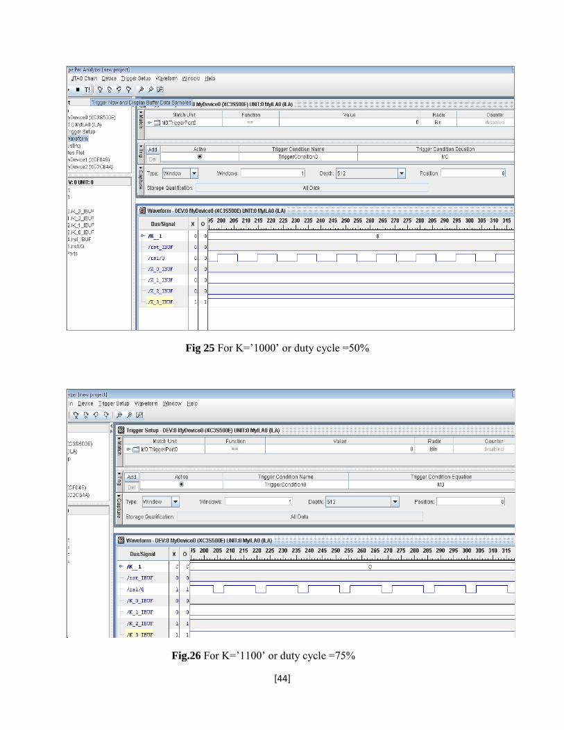
Fig 25: Chipscope Pro result for K=‟1000‟ or duty cycle =50%…………………………………..44
Fig.26: Chipscope Pro result for K=‟1100‟ or duty cycle =75%………………………………….44
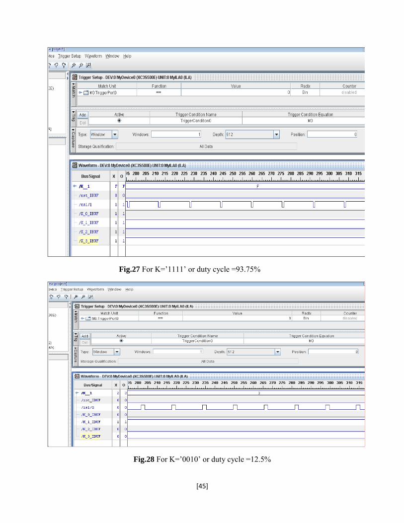
Fig.27 Chipscope Pro result for K=‟1111‟ or duty cycle =93.75%……………………………….45
Fig.28: Chipscope Pro result for K=‟0010‟ or duty cycle =12.5%………………………………...45
List of Tables
Table.1: Macro Statistics of High Frequency Counter based PWM Generator architecture………36
Table.2: Device utilization of High frequency counter based PWM Generator architecture………37
Table.3: Macro Statistics of Counter based PWM Generator architecture…………………………37
Table.4: Device utilization of Counter based PWM Generator architecture………………………..38
Table.5: Macro Statistics of Cascaded Counter based PWM Generator architecture………………38
Table.6: Device utilization of Cascaded Counter based PWM Generator architecture……………39
[7]
ABSTRACT
Pulse Width Modulation has nowadays become an integral part of every electronics system.
These techniques have been widely accepted and are researched extensively nowadays. It has
found its application in large number of applications as a voltage controller. Its use in controlling
output voltage of Inverter is the most frequently used application. There are basically two main
techniques of PWM Generation- Analog technique and Digital Technique.
This thesis deals with these two techniques. First Analog techniques were studied in detail but
these techniques have some demerits. Due to these demerits digital techniques were studied.
Various digital PWM Generator topologies were studied. The VHDL code for each of these
topologies was written and synthesized using Xilinx ISE 10.1 software. Behavioral Simulation
was performed on the architecture and after verifying the results this VHDL code was
downloaded to SPARTAN 3E FPGA. After downloading the code in FPGA real time debugging
was done for the architecture. The results were seen in Chipscope Pro software.
Also from Synthesis report generated after synthesizing the VHDL code of each digital PWM
Generator topologies comparison was done between these topologies in terms of number of logic
blocks used and device utilization of each architecture.
Key Terms : PWM, FPGA, VHDL, Inverter

[8]
Chapter 1
Introduction
[9]
Chapter 1
Introduction
1.1 Introduction
Pulse Width Modulation (PWM) has now become an integral part of almost all embedded
systems. It has been widely accepted as control technique in most of the electronic appliances.
These techniques have been extensively researched during past few years [2]. There are various
methods depending upon architecture and requirement of the system. Their design
implementation depends upon application type, power consumption, semiconductor devices,
performance and cost criteria all determining the PWM method according to N.A. Rahim and Z.
Islam [2].
One of the most important application of PWM lies in power electronics applications for
controlling power converters (DC/DC, DC/AC, etc.) according to E. Koutroulis, A.Dollas and
K.Kalaitzakis in [1]. PWM Inverters are one of those power converters which extensively use
concept of PWM for its operation. PWM inverters are recently showing great popularity for
industrial applications because of their superior performance.
Advancement in designing technology and development in Semiconductor Electronics has led to
this popularity. A numerous PWM schemes are used to obtain variable voltage and frequency
supply.
According to N.A. Rahim and Z. Islam in [2], there are two classes of PWM techniques
identified optimal PWM and carrier PWM. The optimal PWM requires lot of computation and
hence extra hardware and hence extra cost [2] .Carrier PWM techniques require a carrier signal
which is modulated with modulating signal to produce desired PWM signal.

[10]
1.2 PWM Techniques
There are basically two PWM techniques –Analog and Digital Techniques. In analog techniques
there is a carrier signal and a modulating signal. These two signals are compared using
comparator. The output of this comparator is the desired PWM output. There are basically four
analog techniques (a) Sinusoidal PWM (b) Modified Sinusoidal (c) Single Pulse Modulation (d)
Multiple Pulse Modulation. According to [2] and [4]-[7] the disadvantages of these analog
methods are that they are prone to noise and they change with voltage and temperature change.
Also they suffer changes due to component variation [1]. They are less flexible as compared to
digital methods.
Digital methods are the most suited form for designing PWM Generators. They are very flexible
and less sensitive to environmental noise [2]. Also they are simple to construct and can be
implemented very fastly. Most of the digital techniques employ counter and comparator based
circuits. These techniques are discussed in detail in Chapter-4. Analog techniques are discussed
in detail in Chapter-3.
1.3 Advantages of FPGA based design
Field Programmable Gate Array (FPGA) offers the most preferred way of designing PWM
Generator for Power Converter Applications. They are basically interconnection between
different logic blocks. When design is implemented on FPGA they are designed in such a way
that they can be easily modified if any need arise in future. We have to just change the
interconnection between these logic blocks. This feature of Reprogramming capability of FPGA
makes it suitable to make your design using FPGA [1]. Also using FPGA we can implement
design within a short time. Thus FPGA is the best way of designing digital PWM Generators.
Also implementation of FPGA-based digital control schemes prove less costly and hence they
are economically suitable for small designs [1].Hence in this thesis FPGA based PWM
Generator technique is discussed.
[11]
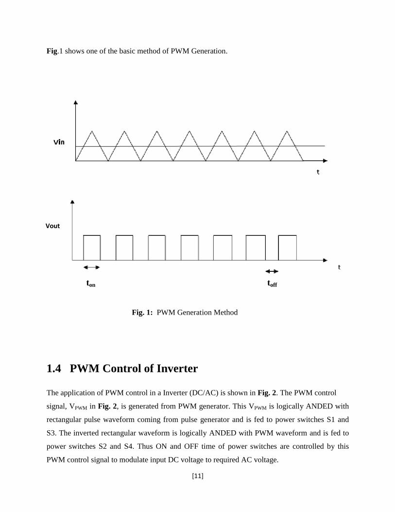
Fig.1 shows one of the basic method of PWM Generation.
Fig. 1: PWM Generation Method
1.4 PWM Control of Inverter
The application of PWM control in a Inverter (DC/AC) is shown in Fig. 2. The PWM control
signal, VPWM in Fig. 2, is generated from PWM generator. This VPWM is logically ANDED with
rectangular pulse waveform coming from pulse generator and is fed to power switches S1 and
S3. The inverted rectangular waveform is logically ANDED with PWM waveform and is fed to
power switches S2 and S4. Thus ON and OFF time of power switches are controlled by this
PWM control signal to modulate input DC voltage to required AC voltage.
Vout
ton toff

[12]
Fig.2 PWM Control of Inverter
The power switch is usually of MOSFET or IGBT. The size of Inverter depends on size of these
power switches. Since frequency of operation is inversely dependent upon Inverter size so we
have to increase the switching frequency to reduce the Inverter size [1]. So we have to look into
the frequency aspect of PWM Generator used so that we get optimized size of Inverter by proper
selection of frequency of PWM wave.
[13]
Chapter 2
Voltage Source
Inverters
[14]
Chapter 2
Voltage Source Inverters
2.1 Definition
Inverters are static power converters that produce an ac output waveform from a dc power supply
according to M.H. Rashid [3]. They are applied in adjustable speed drives (ASDs),
uninterruptible power supplies (UPS), etc. which are its important applications [3]. For
sinusoidal ac outputs, the magnitude, frequency, and phase should be controllable [3]. The
voltage source inverters (VSIs), are the inverters whose independently controlled ac output is a
voltage waveform.
2.2 Single Phase Voltage Source Inverter
Single phase inverters are those inverters which produces only single phase of ac output. Single
phase inverters can be divided into two categories (a) Half Bridge Single Phase Voltage Source
Inverter (b) Full Bridge Single Phase Voltage Source . Although the power range they cover is
the low one, they are widely used in power supplies and single phase UPS and multicell
configurations according to M.H. Rashid [3] .
2.2.1 Half Bridge Voltage Source Inverter(VSI)
Fig.3 shows the circuit configuration of a half bridge VSI. These capacitors are required to filter
out the low order harmonics produced by operation of inverter according to M.H. Rashid [3].
There are two power switches S+ and S- which in Fig.3 are MOSFET‟s. These two switches can
not be ON at the same time because a short circuit across the DC voltage source Vi would be
[15]
produced. To avoid the undefined voltage condition and short circuit we should ensure that either
of the two switches should remain ON.
Fig.3 Single Phase Half Bridge Voltage Source Inverter
When S+ is ON and S- is OFF than inverter power switches , in this case MOSFET, are in
State1 Amplitude of the output voltage is 𝑉𝑖
2 . Similarly when S- is ON and S+ is OFF than
inverter switches are in State 2. Amplitude of the output voltage is - 𝑉𝑖
2 . State 3 is that state in
which both S+ and S- are off.
2.2.2 Full Bridge Voltage Source Inverter (VSI)
Fig.4 shows the circuit configuration of Full Bridge Inverter. There are four power switches
S1+,S1-,S2+ and S2- which are MOSFET in this case.. Switches S1+ and S1- can not be ON at
the same time. Same is the case with switches S2+ and S2-. They can not be ON at the same time
[16]
because short circuit will be produced across DC voltage source Vi. We should avoid undefined
state condition because we always want to define ac output voltage clearly. Output AC voltage
can take value up to Vi which is twice as obtained in Half bridge inverter. This thesis aims at
designing PWM circuit for controlling this full bridge inverter.
Fig.4 Single Phase Full Bridge Voltage Source Inverter
Looking into Fig.4 when switches S1+ and S2- are ON and S1- and S2+ are OFF then inverter is
in state 1. In this state Va= Vi/2 and Vb = -Vi/2 . Since Vo= Va-Vb therefore Vo=Vi for state
1. Similarly when S1- and S2+ are ON and S1+and S2- are OFF then inverter is in state 2 In this
case Vo=-Vi. When S1+ and S2+ are ON and S1- and S2- are OFF then inverter is in state 3. In
this case output voltage Vo of inverter is Vo=0 since both Va and Vb are equal to Vi/2. Similarly
when S1- and S2- are ON and S1+ and S2+ are OFF then inverter is in state 4 and in this case
also V0=0. Last state ,State 5 arises when S1+,S2+,S1- and S2-,are all OFF.
2.3 Pulse Width Modulation in Inverter
Output Voltage of the Inverter can be modified or controlled by controlling or modifying
switching current, or in case of Power Switches, by controlling or modifying Gate current. This
control is achieved by PWM control.
Vb
Va
[17]
In one of the methods of controlling inverter output voltage, a fixed DC voltage is given to the
inverter and by varying the ON and OFF time of power switches we get a controlled or modified
AC output voltage. This method is popularly called as Pulse Width Modulation (PWM) method.
The advantages of the PWM control are:
(1) PWM control is very simple and require very less hardware. So they are also cost
effective.
(2) They can easily implemented using DSP or FPGA.
The major disadvantage of PWM control is that power switches associated with PWM switching
are very costly as their response time should be very fast. So this increases the total cost of
control.
PWM waves are actually pulses of constant amplitude and varying pulse widths. This width can
be varied by different modulation schemes. The most famous of these modulation schemes are
analog methods which are :
(a) Single Pulse Modulation
(b) Sinusoidal Pulse Width modulation
(c) Modified Sinusoidal PWM
(d) Multiple Pulse Width Modulation
All these techniques are discussed in detail in Chapter-3. Here we studied about Inverters and
how to control them using PWM control.

[18]
Chapter 3
Analog techniques of
PWM generation

[19]
Chapter 3
Analog techniques of PWM generation
3 Analog Techniques
Here we will discuss about various analog methods of generating PWM signals. These method
employs the concept of carrier modulation. In this modulation there is one carrier wave which is
basically high frequency triangular pulse train and modulating signal which can be sinusoidal,
DC signal ,etc depending upon which type of modulation is used. Than these two signals are
compared using comparator to give desired PWM output. There are four basic analog modulation
methods : (a) Single Pulse Modulation (b)Sinusoidal Pulse Width modulation (c) Modified
Sinusoidal PWM (d) Multiple Pulse Width Modulation
3.1 Single Pulse Modulation
In this modulation technique a square wave waveform is compared with triangular waveform and
we will get resultant PWM signal. This modulation gives quasi-square wave output. There is
single pulse of output voltage during each half cycle. RMS Value of output voltage can be
controlled by varying the pulse width. The ratio of triangular wave signal amplitude (Pc) and
square wave signal (Pr) is called modulation index i.e. m= 𝑃𝑟
𝑃𝑐 . The width of the pulse can be
changed by varying the modulation index. When m=1 , Square wave output is obtained. The
circuit for this modulation was created in MULTISIM and was simulated in MULTISIM. The
circuit and simulation is shown in Fig.5 and Fig.6 respectively.

[20]
Fig.5 Circuit for Single Pulse Modulation in MULTISIM
Fig.6 Simulation of Single Pulse Modulation in MULTISIM
[21]
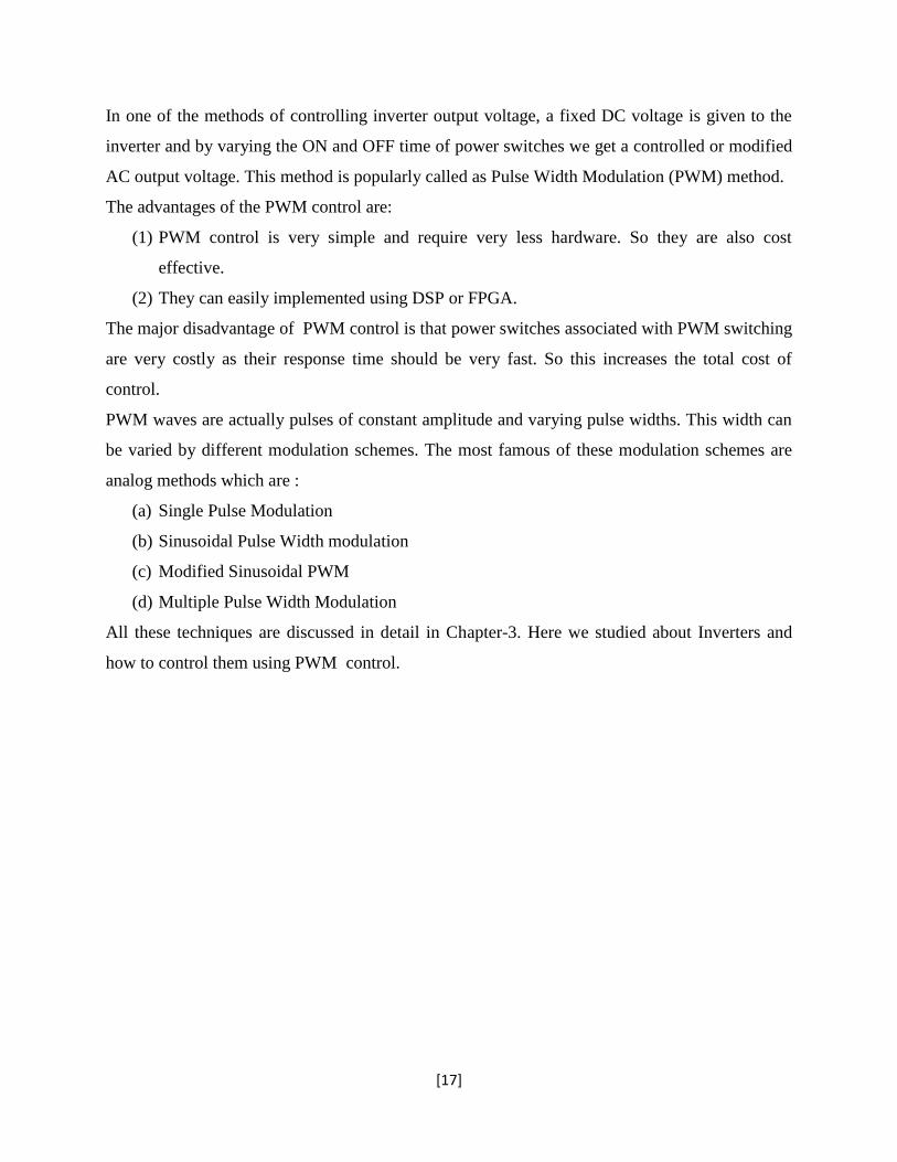
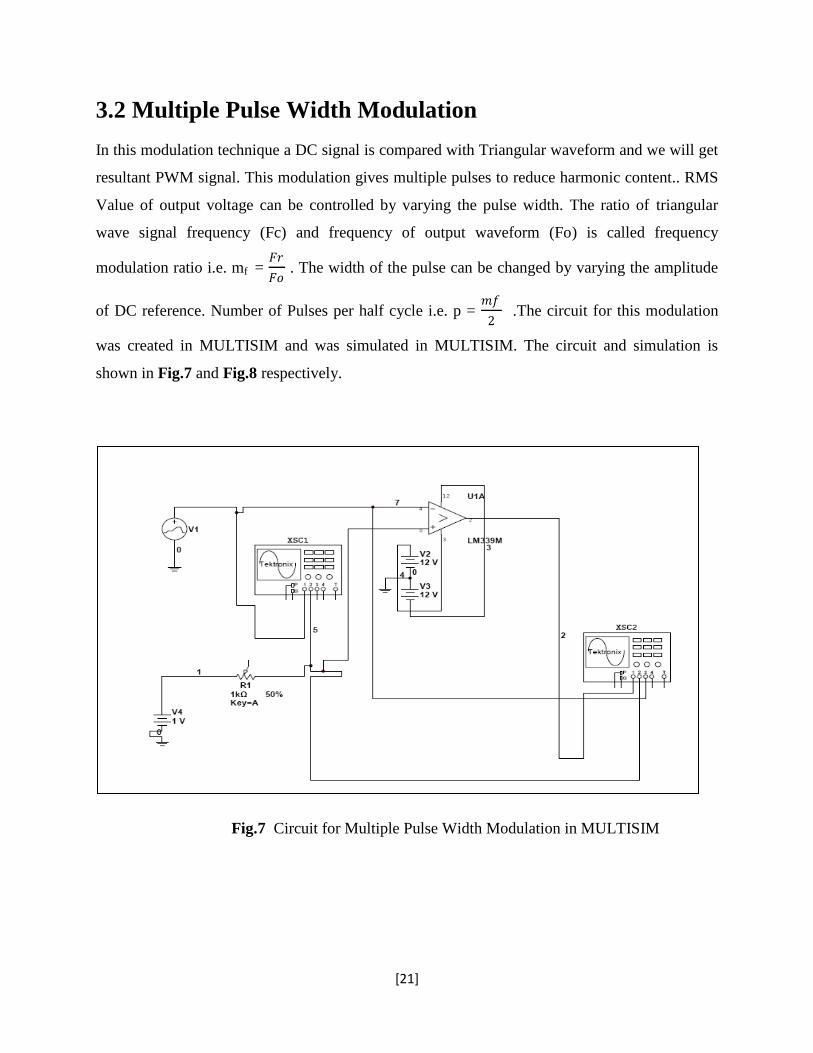
3.2 Multiple Pulse Width Modulation
In this modulation technique a DC signal is compared with Triangular waveform and we will get
resultant PWM signal. This modulation gives multiple pulses to reduce harmonic content.. RMS
Value of output voltage can be controlled by varying the pulse width. The ratio of triangular
wave signal frequency (Fc) and frequency of output waveform (Fo) is called frequency
modulation ratio i.e. mf = 𝐹𝑟
𝐹𝑜 . The width of the pulse can be changed by varying the amplitude
of DC reference. Number of Pulses per half cycle i.e. p = 𝑚𝑓
2 .The circuit for this modulation
was created in MULTISIM and was simulated in MULTISIM. The circuit and simulation is
shown in Fig.7 and Fig.8 respectively.
Fig.7 Circuit for Multiple Pulse Width Modulation in MULTISIM
[22]
Fig.8 Simulation of Multiple Pulse Width Modulation in MULTISIM
3.3 Sinusoidal Pulse Width Modulation
In this modulation technique a sinusoidal signal is compared with Triangular waveform and we
will get resultant PWM signal. The width of each pulse is weighted by the amplitude of sine
wave at that instant. RMS Value of output voltage can be controlled by varying the pulse width.
The ratio of triangular wave signal frequency (Fc) and frequency of output waveform (Fo) is
called frequency modulation ratio i.e. mf = 𝐹𝑟
𝐹𝑜 .. The ratio of triangular wave signal amplitude (Pc)
and sinusoidal wave signal (Pr) is called modulation index i.e. m= 𝑃𝑟
𝑃𝑐 .It is the most widely used
method of voltage control in Inverters. The circuit for this modulation was created in
MULTISIM and was simulated in MULTISIM. The circuit and simulation is shown in Fig.9 and
Fig.10 respectively.

[23]
Fig.9 Circuit for Sinusoidal Pulse Width Modulation in MULTISIM
Fig.10 Simulation of Sinusoidal Pulse Width Modulation in MULTISIM
[24]
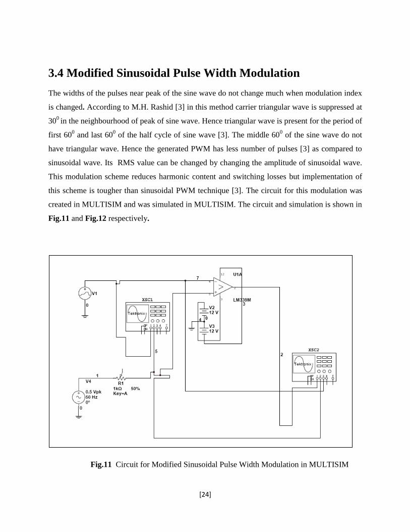
3.4 Modified Sinusoidal Pulse Width Modulation
The widths of the pulses near peak of the sine wave do not change much when modulation index
is changed. According to M.H. Rashid [3] in this method carrier triangular wave is suppressed at
300
in the neighbourhood of peak of sine wave. Hence triangular wave is present for the period of
first 600 and last 60
0 of the half cycle of sine wave [3]. The middle 60
0 of the sine wave do not
have triangular wave. Hence the generated PWM has less number of pulses [3] as compared to
sinusoidal wave. Its RMS value can be changed by changing the amplitude of sinusoidal wave.
This modulation scheme reduces harmonic content and switching losses but implementation of
this scheme is tougher than sinusoidal PWM technique [3]. The circuit for this modulation was
created in MULTISIM and was simulated in MULTISIM. The circuit and simulation is shown in
Fig.11 and Fig.12 respectively.
Fig.11 Circuit for Modified Sinusoidal Pulse Width Modulation in MULTISIM
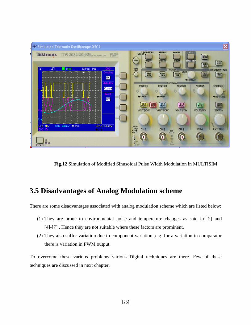
[25]
Fig.12 Simulation of Modified Sinusoidal Pulse Width Modulation in MULTISIM
3.5 Disadvantages of Analog Modulation scheme
There are some disadvantages associated with analog modulation scheme which are listed below:
(1) They are prone to environmental noise and temperature changes as said in [2] and
[4]-[7] . Hence they are not suitable where these factors are prominent.
(2) They also suffer variation due to component variation .e.g. for a variation in comparator
there is variation in PWM output.
To overcome these various problems various Digital techniques are there. Few of these
techniques are discussed in next chapter.

[26]
Chapter 4
Digital Techniques
of PWM Generation
[27]
Chapter 4
Architecture of PWM Generator
4.1 Digital Techniques of PWM Generation
Many digital techniques are based on the use of counter and comparator based design. These
digital techniques are easier to implement than analog techniques. Also they are immune to
environmental noise and temperature change. Also they do not suffer component variation and
switching losses.. For sophisticated control schemes it is desirable to use Digital PWM
modulation scheme.
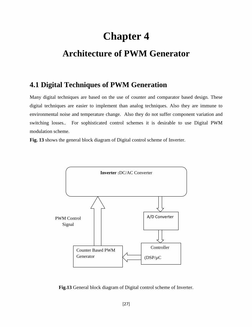
Fig. 13 shows the general block diagram of Digital control scheme of Inverter.
Fig.13 General block diagram of Digital control scheme of Inverter.
Inverter :DC/AC Converter
A/D Converter
Controller
(DSP/µC
Counter Based PWM
Generator
PWM Control
Signal

[28]
There are many digital techniques available depending upon the arrangement and type of counter
used but in this chapter three main PWM Generator topologies are discussed. These are (a) High
frequency counter based PWM generator (b) Counter based PWM generator (c) Cascaded
Counter based PWM generator.
4.2 High frequency counter based PWM Generator
This architecture was proposed by E.Koutroulis , A.Dollas and K.Kalaitzakis in [1]. According
to this architecture there is a high speed N-bit free running counter whose output is compared
with register output; which stores desired input duty cycle( N-bit value); with the help of
comparator. The comparator output is set equal to 1 when both these values are equal. This
comparator output is used to set RS latch .The overflow signal from counter is used to reset RS
latch. The output of RS latch gives the desired PWM output.. This overflow signal is also used to
load new N-bit duty cycle in Register.
The advantage of these method is that it is used to generate High-frequency PWM output which
is not possible in normal counter based approach. Fig.14 shows the corresponding block diagram
of this architecture.
Fig.14 Architecture of PWM Generator proposed by E. Koutroulis et al. in [1]
[29]
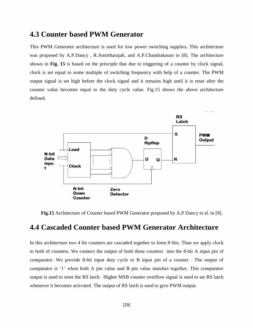
4.3 Counter based PWM Generator
This PWM Generator architecture is used for low power switching supplies. This architecture
was proposed by A.P.Dancy , R.Amirtharajah, and A.P.Chandrakasan in [8]. The architecture
shown in Fig. 15 is based on the principle that due to triggering of a counter by clock signal,
clock is set equal to some multiple of switching frequency with help of a counter. The PWM
output signal is set high before the clock signal and it remains high until it is reset after the
counter value becomes equal to the duty cycle value. Fig.15 shows the above architecture
defined.
Fig.15 Architecture of Counter based PWM Generator proposed by A.P Dancy et al. in [8].
4.4 Cascaded Counter based PWM Generator Architecture
In this architecture two 4 bit counters are cascaded together to form 8 bits. Than we apply clock
to both of counters. We connect the output of both these counters into the 8-bit A input pin of
comparator. We provide 8-bit input duty cycle to B input pin of a counter . The output of
comparator is „1‟ when both A pin value and B pin value matches together. This comparator
output is used to reset the RS latch. Higher MSB counter overflow signal is used to set RS latch
whenever it becomes activated. The output of RS latch is used to give PWM output.

[30]
Here we discussed various topologies of digital PWM Generator. In next chapter we will see
what were the steps followed to design and download PWM Generator architecture in FPGA.
[31]
Chapter 5
Design Procedure
on FPGA

[32]
Behavioral
Simulation
Design
Synthesis
Xilinx Device
(FPGA)
Programming
Chapter 5
Design Procedure on FPGA
5.1 FPGA basics
The Field Programmable Gate Array (FPGA) ,as the name suggest, is a array of logic cells (or
modules) and interconnects, which can be reprogrammed depending upon the requirement of the
user. We can design it and make changes in it whenever required. It provides instant
manufacturing turnaround and negligible prototype costs which makes it suitable for embedded
system design.
5.2 FPGA Design Flow
Fig.16 FPGA Design Flow
Design Entry
Design
Implementation
Map
Place and Route
Translate
[33]
Fig.16 shows the sequence of steps followed when implementing PWM Generator design on
FPGA. These steps are discussed in detail here.
4.2.1 Design Entry
This is the first step of implementing a design on FPGA. In this step the VHDL (Very High
Speed Integrated Chip Hardware Description Language) code of PWM Generator Architecture
was written using software Xilinx ISE 10.1. Structural modeling was used for writing the code.
After writing the code syntax check was performed on the code to see whether code was properly
written using correct syntax
4.2.2 Behavioral Simulation
The next step is behavioral simulation. This step verifies whether the design entered is
functionally correct or not. This simulation is called RTL simulation. For this simulation VHDL
Testbench was written for PWM Generator architecture and simulation was seen in Xilinx ISE
Simulator. After it is verified it is functionally correct we move onto next step.
4.2.3 Design Synthesis
The VHDL code of PWM Generator is then synthesized using Xilinx XST which is a part of
Xilinx ISE software. There is a option of Synthesis in process tab of Xilinx ISE which performs
the operation of synthesis .The synthesis process is used for optimizing the design architecture
selected. The resulting netlist is saved to an NGC file. After design synthesis, synthesis report is
generated which gives information about how many logic blocks are used and what is the device
utilization of the design architecture synthesized. Synthesis basically maps the behavioral design
to gate level design.
4.2.4 Design Implementation
After design synthesis ,design implementation is done which comprises of following three steps
(a) Translate
(b) Map
(c) Place and Route
Before translating the design, User Constrained file (UCF) is written to assign pin configuration
of the FPGA to the PWM Generator I/O‟s. Once this is done Translate merges together this UCF
file and netlist generated after synthesis into Xilinx design file
Mapping is done to fit the design into the available resources of target device i.e. FPGA. This is
also important step of design.

[34]
Last step of Design Implementation is Placing and Routing which places the logic blocks of the
design into FPGA and route them together so that they occupy minimum area and meet timing
requirements. This operation produces NCD output file.
4.2.5 Xilinx Device (FPGA) Programming
There is a option of Generate programming file on the process tab of Xilinx ISE which converts
the NCD file generated after routing to BIT file. It produces a bitstream for Xilinx Device
(FPGA in this case ) configuration. This BIT file is used to program the FPGA.
4.2.6 Configuring Target Device
There is option of Generate Target PROM/ACE on the process tab of Xilinx ISE which converts
the BIT file to the PROM or ACE file. This PROM or ACE file can be downloaded directly into
the FPGA‟s memory cells.
We have to make sure that FPGA is connected to the PC where we are developing this design.
After we download PROM or ACE file into the FPGA the FPGA is ready to be used as PWM
Generator. We can give different input combination to see how the output of FPGA varies. This
input can be given by switches whose pin number has been assigned to PWM generator input.
The output can be seen by LED whose pin number has been assigned to PWM Generator output.
In next chapter different results and simulation obtained are shown for PWM generator. Given
below is the figure of SPARTAN 3E FPGA used in this project.
Fig.17 SPARTAN-3E Starter Kit (FPGA)

[35]
Chapter 6
Results and
Simulation
[36]
Chapter 6
Results and Simulation
6.1 Results
Design steps discussed in last chapter were followed to implement design of PWM generator on
FPGA. Different topologies of PWM Generator discussed in Chapter-4 were implemented.
Given below are the various tables generated after synthesizing various PWM Generator
topologies .
6.1.1 Synthesis Report of High Frequency Counter based
PWM Generator
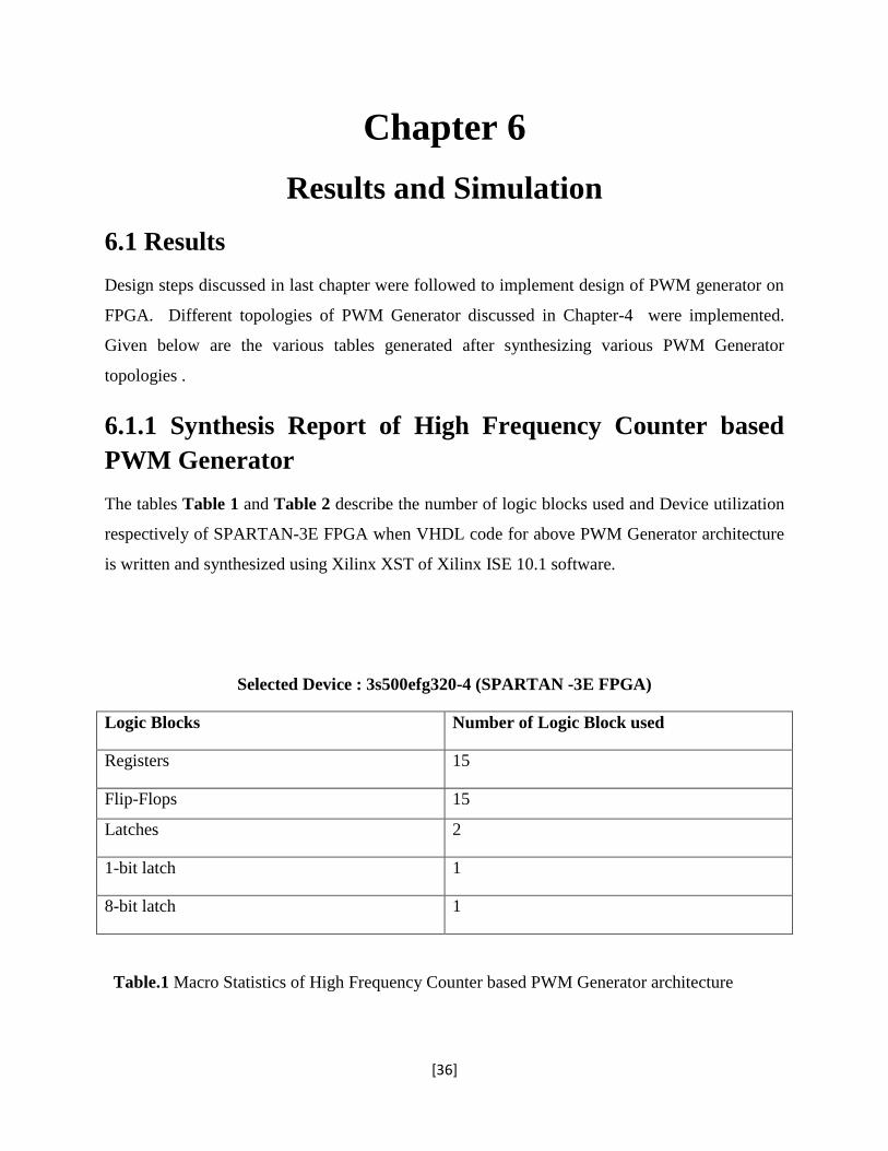
The tables Table 1 and Table 2 describe the number of logic blocks used and Device utilization
respectively of SPARTAN-3E FPGA when VHDL code for above PWM Generator architecture
is written and synthesized using Xilinx XST of Xilinx ISE 10.1 software.
Selected Device : 3s500efg320-4 (SPARTAN -3E FPGA)
Logic Blocks Number of Logic Block used
Registers 15
Flip-Flops 15
Latches 2
1-bit latch 1
8-bit latch 1
Table.1 Macro Statistics of High Frequency Counter based PWM Generator architecture
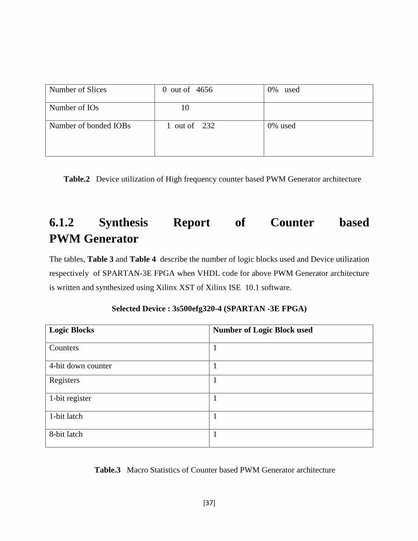
[37]
Number of Slices 0 out of 4656 0% used
Number of IOs 10
Number of bonded IOBs 1 out of 232 0% used
Table.2 Device utilization of High frequency counter based PWM Generator architecture
6.1.2 Synthesis Report of Counter based
PWM Generator
The tables, Table 3 and Table 4 describe the number of logic blocks used and Device utilization
respectively of SPARTAN-3E FPGA when VHDL code for above PWM Generator architecture
is written and synthesized using Xilinx XST of Xilinx ISE 10.1 software.
Selected Device : 3s500efg320-4 (SPARTAN -3E FPGA)
Logic Blocks Number of Logic Block used
Counters 1
4-bit down counter 1
Registers 1
1-bit register 1
1-bit latch 1
8-bit latch 1
Table.3 Macro Statistics of Counter based PWM Generator architecture
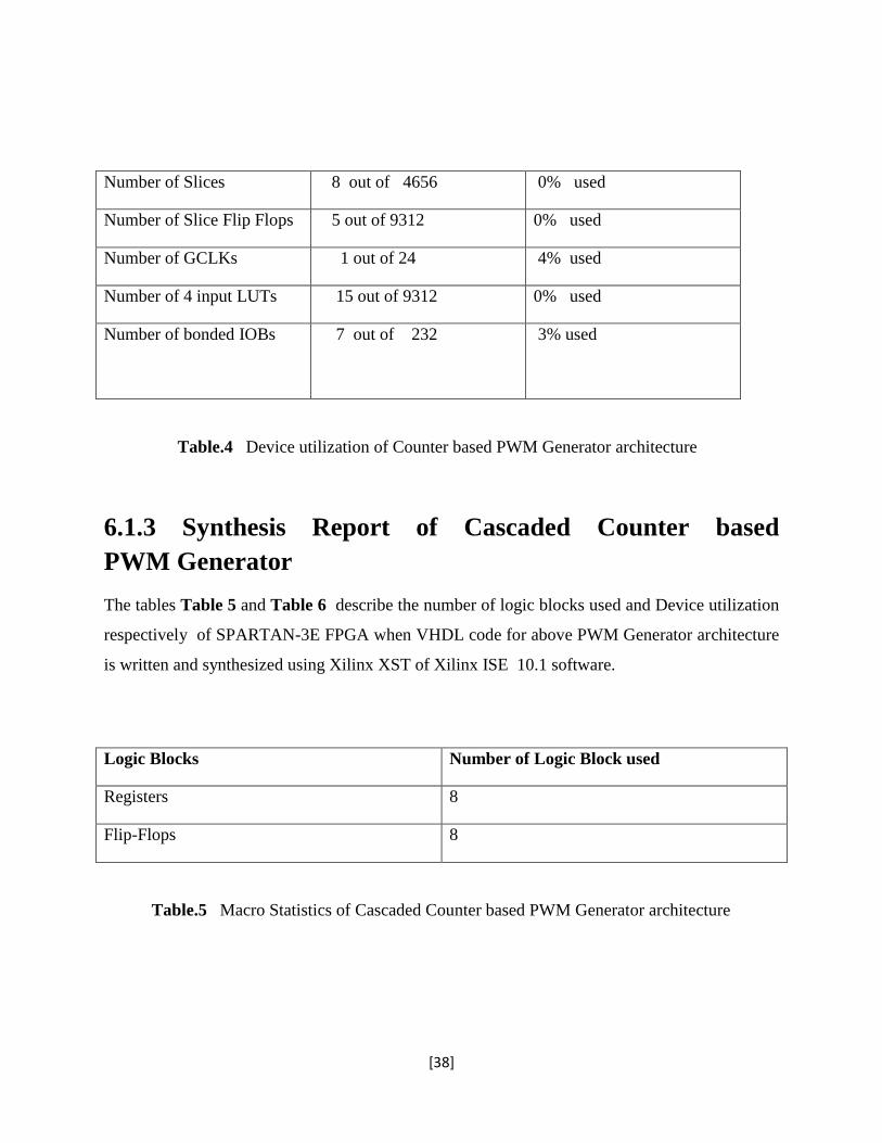
[38]
Table.4 Device utilization of Counter based PWM Generator architecture
6.1.3 Synthesis Report of Cascaded Counter based
PWM Generator
The tables Table 5 and Table 6 describe the number of logic blocks used and Device utilization
respectively of SPARTAN-3E FPGA when VHDL code for above PWM Generator architecture
is written and synthesized using Xilinx XST of Xilinx ISE 10.1 software.
Logic Blocks Number of Logic Block used
Registers 8
Flip-Flops 8
Table.5 Macro Statistics of Cascaded Counter based PWM Generator architecture
Number of Slices 8 out of 4656 0% used
Number of Slice Flip Flops 5 out of 9312 0% used
Number of GCLKs 1 out of 24 4% used
Number of 4 input LUTs 15 out of 9312 0% used
Number of bonded IOBs 7 out of 232 3% used
[39]
Number of Slices 8 out of 4656 0% used
Number of Slice Flip Flops 9 out of 9312 0% used
Number of GCLKs 1 out of 24 4% used
Number of 4 input LUTs 13 out of 9312 0% used
Number of bonded IOBs 10 out of 232 4% used
Number of IO‟s 10
IOB Flip Flops 1
Table.6 Device utilization of Cascaded Counter based PWM Generator architecture
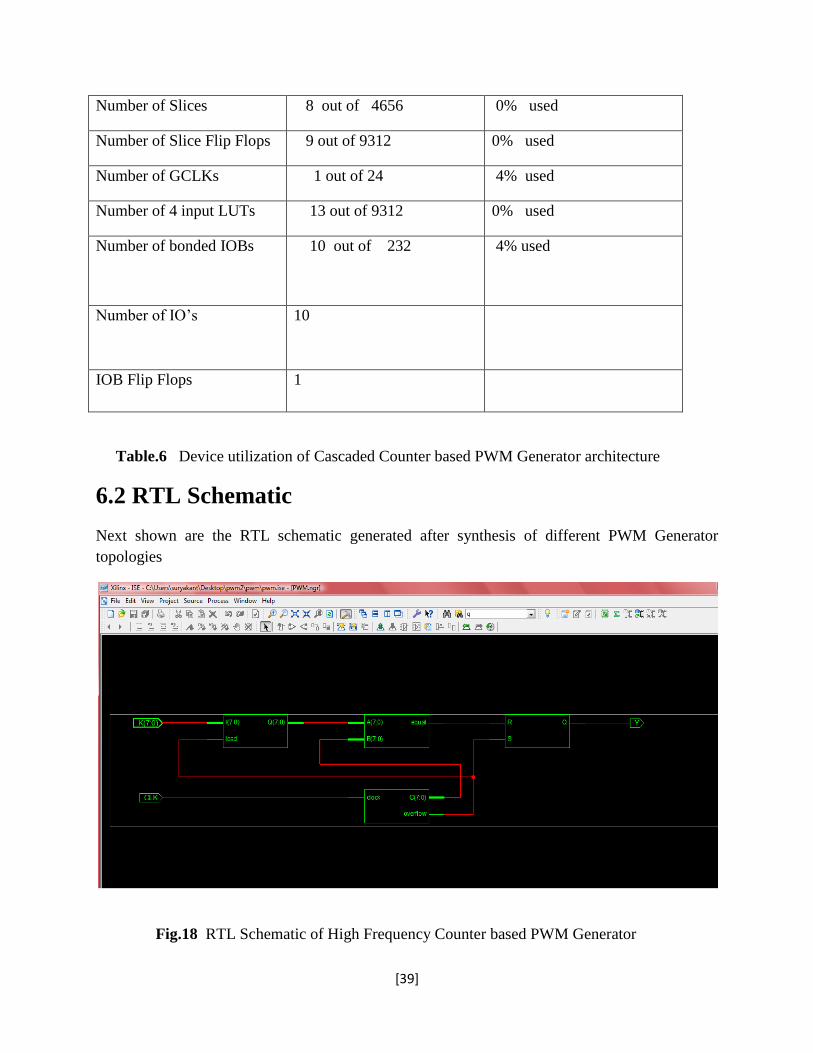
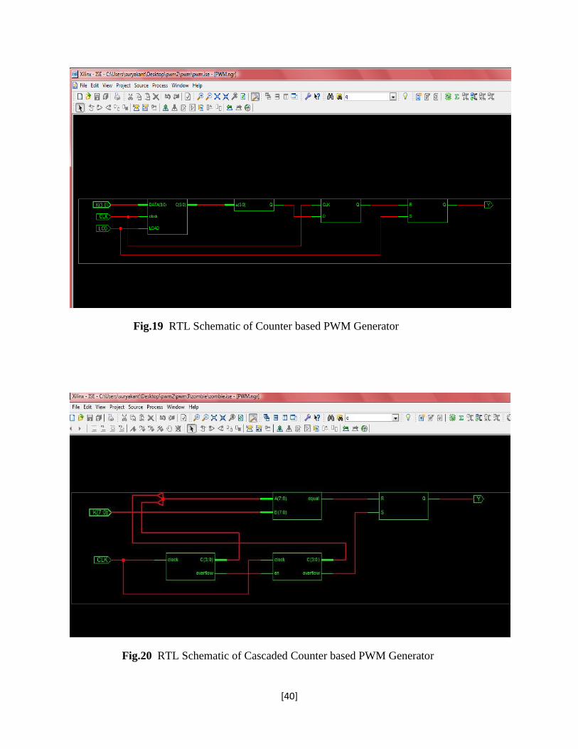
6.2 RTL Schematic
Next shown are the RTL schematic generated after synthesis of different PWM Generator
topologies
Fig.18 RTL Schematic of High Frequency Counter based PWM Generator
[40]
Fig.19 RTL Schematic of Counter based PWM Generator
Fig.20 RTL Schematic of Cascaded Counter based PWM Generator

[41]
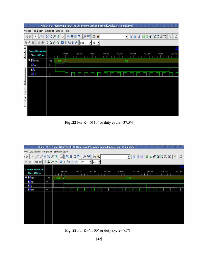
6.3 Simulation
The Xilinx ISE simulator was used for functional verification of PWM Generator topologies.
The resulting simulations for 4-bit data input configuration of PWM generation unit for different
duty cycle is shown below in Fig.21 to Fig.23. The duty cycle is calculated as below
Duty Cycle = 𝐼𝑛𝑡𝑔𝑒𝑟 𝑉𝑎𝑙𝑢𝑒 𝑜𝑓 4−𝑏𝑖𝑡 𝐾 𝑤𝑜𝑟𝑑
16
Where K is the 4-bit input to PWM Generator. Suppose the value of input data word to PWM
Unit K=‟1001‟ than Duty Cycle = 9
16 = 0.5625 OR 56.25% duty cycle.
Fig .21 For input value K =‟0100‟ or duty cycle=25%
[42]
Fig .22 For K=‟0110‟ or duty cycle =37.5%
Fig .23 For K=‟1100‟ or duty cycle= 75%
[43]
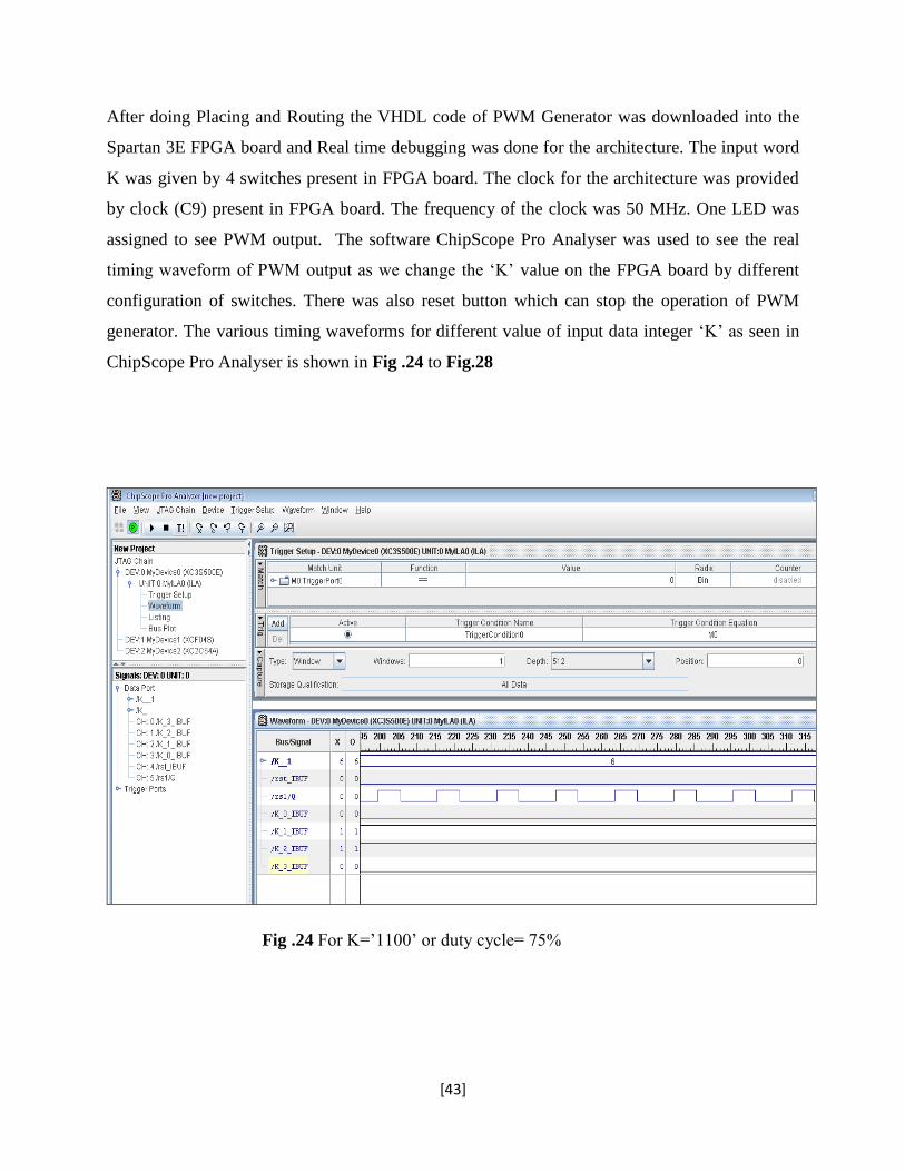
After doing Placing and Routing the VHDL code of PWM Generator was downloaded into the
Spartan 3E FPGA board and Real time debugging was done for the architecture. The input word
K was given by 4 switches present in FPGA board. The clock for the architecture was provided
by clock (C9) present in FPGA board. The frequency of the clock was 50 MHz. One LED was
assigned to see PWM output. The software ChipScope Pro Analyser was used to see the real
timing waveform of PWM output as we change the „K‟ value on the FPGA board by different
configuration of switches. There was also reset button which can stop the operation of PWM
generator. The various timing waveforms for different value of input data integer „K‟ as seen in
ChipScope Pro Analyser is shown in Fig .24 to Fig.28
Fig .24 For K=‟1100‟ or duty cycle= 75%
[44]
Fig 25 For K=‟1000‟ or duty cycle =50%
Fig.26 For K=‟1100‟ or duty cycle =75%
[45]
Fig.27 For K=‟1111‟ or duty cycle =93.75%
Fig.28 For K=‟0010‟ or duty cycle =12.5%

[46]
Chapter 7
Conclusion and
Future Work

[47]
Chapter 6
Conclusion and Future Work
7.1 Conclusion
Various PWM Generator topologies were studied and they were synthesized using Xilinx ISE
software. Device Utilization and No of Logic Blocks of each topology were noted down and
compared with each other. It was seen that number of logic blocks used in FPGA for design of
PWM Generator is minimum in case of Counter based PWM Generator and maximum in case of
High frequency Counter based PWM generator. Device (FPGA) utilization is best for Cascaded
Counter based PWM Generator and minimum for High frequency Counter based PWM
generator. Functional verification was also performed on VHDL code of PWM Generator and
simulation was observed as given in Fig 21 to Fig.23. After downloading the design into the
SPARTAN 3E FPGA board Real Time Debugging was performed on this architecture and
results were observed in Chipscope Pro Analyzer. These timing waveforms are shown in Fig.24
to Fig.28
7.2 Future Work
PWM Generator architecture which was downloaded onto FPGA can be used to control Gate
signal of Power Switches of Inverter. By this way we can be able to control ON and OFF time of
Inverter. Hence we can use this architecture for controlling Inverter which produces AC from
DC source. Hence we can implement PWM Inverter from this FPGA based PWM Generator.
[48]
References
[1] Koutroulis E., Dollas A. and Kalaitzakis K., “High-frequency pulse width modulation
implementation using FPGA and CPLD ICs”, Journal of Systems Architecture , Vol.52 (2006):
pp. 332–344
[2] Rahim N.A. and Islam Z., “Field Programmable Gate Array-Based Pulse-Width Modulation
for Single Phase Active Power Filter”; American Journal of Applied Sciences, Vol.6 (2009): pp.
1742-1747
[3] Rashid M.H., Power Electronics Handbook. Florida, Academic Press, 2001
[4] Retif J.M., Allard B., Jorda X. and Perez A, “Use of ASIC‟s in PWM techniques for power
converters”, Proceedings of the International Conference on Industrial Electronics, Control and
Instrumentation, IEEE Xplore Press, Maui, HI, USA.,(1993) pp: 683-688. DOI:
10.11.09/IECON.1993.338998
[5] Tzou, Y.Y., H.J. Hsu, T.S. Kuo, “FPGA based SVPWM control IC for 3-phase PWM
inverters”, Proceedings of the IEEE 22nd International Conference on Industrial Electronics,
Control and Instrumentation, IEEE Xplore Press, Taipei, Taiwan, (1996): pp: 138-148. DOI:
10.11.09/IECON.1996.570921
[6] Bowes S.R. and Midoun A., “Suboptimal switching strategies for microprocessor-controlled
PWM inverter drives”, IEE Proc. B. Elect. Power Appli., Vol.132(1985),: pp.133-148. DOI:
10.1049/ip-b:19850019
[7] Rahim, N.A. and Islam Z.,”A single-phase series active power filter design”, Proceeding of
the International Conference on Electrical, Electronic and Computer Engineering, IEEE Xplore
Press ,Sept. 2004, pp: 926-929
[8] Dancy A.P., Amirtharajah R. and Chandrakasan A.P., “High-Efficiency Multiple-Output
DC–DC Conversion for Low-Voltage Systems”, IEEE Trans. on Very Large Scale Integration
(VLSI) Systems, Vol. 8, No. 3, June 2000: pp.252-263
[9] Cheng J., Witulski A. and Vollin J., “A small-signal model utilizing amplitude modulation
for the Class-D converter at fixed frequency”, IEEE Trans. on Power Electronics ,Vol.15
(2000),pp. 1204–1211.