fpga and asic implementation of rho and p-1 methods...
TRANSCRIPT

FPGA AND ASIC IMPLEMENTATION OF RHO AND P-1 METHODS OF FACTORING
by
Ramakrishna Bachimanchi A Thesis
Submitted to the Graduate Faculty
of George Mason University
In Partial fulfillment of The Requirements for the Degree
of Master of Science
Computer Engineering
Committee:
_________________________________ Dr. Kris Gaj, Thesis Director
_________________________________ Dr. Rao Mulpuri, Committee Member
_________________________________ Dr. Jens-Peter Kaps, Committee Member
_________________________________ Andre Manitius, Chairman, Department Electrical and Computer Engineering
_________________________________ Lloyd J. Griffiths, Dean, The Volgenau School of Information Technology and Engineering
Date: _____________________________ Spring Semester 2007 George Mason University Fairfax, Virginia

FPGA and ASIC Implementation of rho and p-1 methods of factoring
A thesis submitted in partial fulfillment of the requirements for the degree of Master of Science at George Mason University
By
Ramakrishna Bachimanchi Bachelor of Engineering
Osmania University, 2004
Director: Dr. Kris Gaj, Associate Professor Department of Electrical and Computer Engineering
Spring Semester 2007 George Mason University
Fairfax, VA

ii
Copyright © 2007 by Ramakrishna Bachimanchi All Rights Reserved

iii
ACKNOWLEDGEMENTS
I would like to thank Dr. Kris Gaj for helping me throughout the course of this research. Special thanks to Dr. Soonhak Kwon, Dr. Patrick Baier, Paul Kohlbrenner, Hoang Le and Mohammed Khaleeluddin.

iv
TABLE OF CONTENTS
PAGE
ABSTRACT ............................................................................................................................................. viii
CHAPTER 1: INTRODUCTION .................................................................................................................... 1
1.1 PUBLIC KEY CRYPTOSYSTEMS .................................................................................................................. 1 1.2 RSA AND ITS SECURITY.......................................................................................................................... 2 1.3 GOALS OF THIS THESIS .......................................................................................................................... 4
CHAPTER 2: CO-FACTORING PHASE OF NUMBER FIELD SIEVE: OVERVIEW AND ALGORITHMS ................. 6
2.1 RHO METHOD .................................................................................................................................... 6 2.2 P-1 METHOD: OVERVIEW AND ALGORITHM ............................................................................................. 10 2.3 ECM METHOD ................................................................................................................................. 12 2.4 BASIC OPERATIONS ............................................................................................................................ 14
2.4.1 Montgomery Multiplication ................................................................................................... 14 2.4.2 Exponentiation Algorithms .................................................................................................... 16
CHAPTER 3: PROPOSED ARCHITECTURE OF CO-FACTORING CIRCUIT...................................................... 18
3.1 TOP LEVEL VIEW ............................................................................................................................... 19 3.2 IMPLEMENTATION OF BASIC ARITHMETIC OPERATIONS ............................................................................... 20
3.2.1 Modular Addition and Subtraction ........................................................................................ 21 3.2.2 Montgomery Multiplier ......................................................................................................... 24
CHAPTER 4: ARCHITECTURE OF RHO AND P-1 ........................................................................................ 29
4.1 PARTITIONING OF OPERATIONS BETWEEN HARDWARE AND SOFTWARE ............................................................ 29 4.2 HARDWARE ARCHITECTURE OF RHO METHOD .......................................................................................... 32 4.3 HARDWARE ARCHITECTURE OF P-1 METHOD ........................................................................................... 38 4.4 GLOBAL MEMORY MAPS..................................................................................................................... 41
4.4.1 Rho ....................................................................................................................................... 41 4.4.2 P-1 ........................................................................................................................................ 43 4.4.3 Unified rho and p-1 ............................................................................................................... 44
4.4 LOCAL MEMORY MAPS ....................................................................................................................... 44 4.4.1 Medium level operations ....................................................................................................... 44 4.4.2 Rho ....................................................................................................................................... 45 4.4.3 P-1 ........................................................................................................................................ 46 4.4.4 Unified rho and p-1 ............................................................................................................... 49
4.5 CONTROL UNIT ................................................................................................................................. 49 4.5.1 Rho ....................................................................................................................................... 49 4.5.2 P-1 ........................................................................................................................................ 51 4.5.3 Unified Unit ........................................................................................................................... 53
CHAPTER 5: FPGA IMPLEMENTATION AND VERIFICATION ..................................................................... 54

v
5.1 OVERVIEW OF FPGA FAMILIES ............................................................................................................. 54 5.2 FPGA DESIGN FLOW ......................................................................................................................... 55 5.3 TOOLS AND VERIFICATION METHODOLOGY .............................................................................................. 57
CHAPTER 6: ASIC IMPLEMENTATION AND VERIFICATION ....................................................................... 59
6.1 ASIC DESIGN FLOW ........................................................................................................................... 59 6.2 PORTING DESIGNS FROM FPGA TO ASIC ................................................................................................ 62 6.3 TOOLS AND LIBRARIES ........................................................................................................................ 62
6.3.1 Tools ..................................................................................................................................... 62 6.3.2 LIBRARIES ..................................................................................................................................... 62
CHAPTER 7: RESULTS .............................................................................................................................. 63
7.1 FPGA RESULTS ................................................................................................................................. 63 7.1.1 Memory Requirements .......................................................................................................... 64
7.1.1.1 P-1 ................................................................................................................................................64 7.1.1.2 Rho ...............................................................................................................................................66 7.1.1.3 Unified rho and p-1 ........................................................................................................................67
7.1.2 Timing Calculations for rho, p-1 and unified unit .................................................................... 68 7.1.2.1 Rho ...............................................................................................................................................68 7.1.2.2 P-1 ................................................................................................................................................69 7.1.2.3 Unified rho and p-1 ........................................................................................................................71
7.1.3 Area and Timing results from FPGA implementations............................................................. 71 7.2 AREA AND TIMING RESULTS FROM ASIC IMPLEMENTATIONS ........................................................................ 76 7.3 COMPARISON OF FPGA AND ASIC RESULTS ............................................................................................ 78
CHAPTER 8: SUMMARY AND CONCLUSION ............................................................................................ 79
BIBLIOGRAPHY ....................................................................................................................................... 82
CURRICULUM VITAE ............................................................................................................................... 84
vi
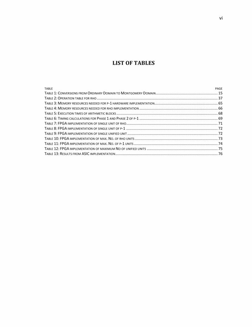
LIST OF TABLES
TABLE PAGE TABLE 1: CONVERSIONS FROM ORDINARY DOMAIN TO MONTGOMERY DOMAIN......................................................... 15 TABLE 2: OPERATION TABLE FOR RHO ............................................................................................................... 37 TABLE 3: MEMORY RESOURCES NEEDED FOR P-1 HARDWARE IMPLEMENTATION.......................................................... 65 TABLE 4: MEMORY RESOURCES NEEDED FOR RHO IMPLEMENTATION ........................................................................ 66 TABLE 5: EXECUTION TIMES OF ARITHMETIC BLOCKS ............................................................................................. 68 TABLE 6: TIMING CALCULATIONS FOR PHASE 1 AND PHASE 2 OF P-1 ........................................................................ 69 TABLE 7: FPGA IMPLEMENTATION OF SINGLE UNIT OF RHO.................................................................................... 71 TABLE 8: FPGA IMPLEMENTATION OF SINGLE UNIT OF P-1 .................................................................................... 72 TABLE 9: FPGA IMPLEMENTATION OF SINGLE UNIFIED UNIT ................................................................................... 72 TABLE 10: FPGA IMPLEMENTATION OF MAX. NO. OF RHO UNITS ............................................................................ 73 TABLE 11: FPGA IMPLEMENTATION OF MAX. NO. OF P-1 UNITS ............................................................................. 74 TABLE 12: FPGA IMPLEMENTATION OF MAXIMUM NO OF UNIFIED UNITS ................................................................. 75 TABLE 13: RESULTS FROM ASIC IMPLEMENTATION .............................................................................................. 76

vii
LIST OF FIGURES
FIGURE PAGE
FIGURE 1: STEPS OF NFS................................................................................................................................. 3 FIGURE 2: PATTERN OF RHO ............................................................................................................................ 7 FIGURE 3: PROPOSED ARCHITECTURE FOR CO-FACTORING ...................................................................................... 19 FIGURE 4: BLOCK DIAGRAM OF THE ADDER/SUBTRACTOR ...................................................................................... 23 FIGURE 5: CASCADED OF TWO CARRY SAVE ADDERS, REDUCING FOUR OPERANDS TO TWO .............................................. 25 FIGURE 6: BLOCK DIAGRAM OF THE MULTIPLIER .................................................................................................. 26 FIGURE 7: TOP LEVEL BLOCK DIAGRAM .............................................................................................................. 31 FIGURE 8: GRAPHICAL REPRESENTATION OF ORIGINAL POLLARD’S RHO...................................................................... 33 FIGURE 9: GRAPHICAL REPRESENTATION OF IMPROVED VERSION BY BRENT ................................................................ 35 FIGURE 10: SEQUENCE OF OPERATIONS IN HARDWARE FOR BRENT’S RHO .................................................................. 37 FIGURE 11: CONTENTS OF GLOBAL MEMORY FOR RHO .......................................................................................... 42 FIGURE 12: CONTENTS OF GLOBAL MEMORY FOR P-1 A) PHASE 1 B) PHASE 2 ............................................................. 43 FIGURE 13: CONTENTS OF LOCAL MEMORY OF RHO .............................................................................................. 46 FIGURE 14: LOCAL MEMORY OF P-1 ................................................................................................................. 47 FIGURE 15: CONTENTS OF LOCAL MEMORY OF P-1 A) PHASE 1 B) PHASE 2 ................................................................. 48 FIGURE 16: FPGA DESIGN FLOW .................................................................................................................... 56 FIGURE 17: ASIC DESIGN FLOW ...................................................................................................................... 60 FIGURE 18: PHYSICAL DESIGN FLOW OF ASIC ...................................................................................................... 61
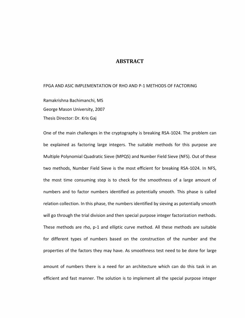
ABSTRACT
FPGA AND ASIC IMPLEMENTATION OF RHO AND P-1 METHODS OF FACTORING
Ramakrishna Bachimanchi, MS
George Mason University, 2007
Thesis Director: Dr. Kris Gaj
One of the main challenges in the cryptography is breaking RSA-1024. The problem can
be explained as factoring large integers. The suitable methods for this purpose are
Multiple Polynomial Quadratic Sieve (MPQS) and Number Field Sieve (NFS). Out of these
two methods, Number Field Sieve is the most efficient for breaking RSA-1024. In NFS,
the most time consuming step is to check for the smoothness of a large amount of
numbers and to factor numbers identified as potentially smooth. This phase is called
relation collection. In this phase, the numbers identified by sieving as potentially smooth
will go through the trial division and then special purpose integer factorization methods.
These methods are rho, p-1 and elliptic curve method. All these methods are suitable
for different types of numbers based on the construction of the number and the
properties of the factors they may have. As smoothness test need to be done for large
amount of numbers there is a need for an architecture which can do this task in an
efficient and fast manner. The solution is to implement all the special purpose integer

factorization methods in hardware and then integrate them together. Elliptic curve
method of factoring was implemented in hardware and presented in the thesis
submitted by Mohammed Khaleeluddin. In this thesis I implemented the remaining
methods, which are rho and p-1, and I developed a unified architecture combining rho
and p-1. These two methods and the integrated unit all are implemented in two
technologies, FPGA and ASIC. In FPGA, low cost devices Spartan 3 and Spartan 3E
outperform high performance devices Virtex II and Virtex 4 in terms of performance to
cost ratio, thus most suitable for code-breaking. ASIC implementation resulted in higher
frequency and more area efficient than FPGA. When large amount of ASIC chips are
manufactured to overcome the non-recurring cost of fabrication, ASIC has an edge over
FPGA. Low cost FPGA devices are the best choice, when large amount of chips are not
considered.

1
Chapter 1: Introduction
Cryptography (“secret writing”, from the Greek kryptós, “hidden,” and gráfo “write”) is
the study of message secrecy. It refers to encryption, which is the process of scrambling
or obscuring the ordinary messages (plaintext), such that they are not easily readable
(have a form of a randomly looking stream of bits called ciphertext). The process reverse
to encryption is decryption, which recovers the original message (plaintext) from the
encrypted message (cipher text). An algorithm that defines both encryption and
decryption is called a cryptosystem. Cryptosystems are mainly categorized into Secret
Key (or symmetric) cryptosystem and Public Key (or asymmetric) cryptosystems. In all
cryptosystems encryption and decryption depend on a key (or a pair of keys) which
changes their detailed operation.
1.1 Public Key Cryptosystems
In secret key cryptosystems the same secret key is used for both encryption and
decryption. The difficult and challenging task in this cryptosystem is to agree on the
same secret key without any third party knowing the value of the key. Anyone who finds
out the key can intercept the message in the middle, as well as read, modify or forge the
2
information. The process of generating, transmitting and storing all the keys is known as
key management. One of the main challenges or difficulties of the symmetric
cryptosystems is securing the key management.
In public key cryptosystems each user is supplied with a public key and private key. In
these cryptosystems, message is encrypted using recipient’s public key and can only be
decrypted using intended recipient’s private key. Public key may be published but the
private key should be kept secret. Public and private keys are related mathematically
and deriving the private key from public key is difficult and not practical. As all the
communications make use of the public key, the problem of sharing a secret key
between sender and receiver can be avoided.
1.2 RSA and its security
RSA is one of the first and great developments in public key cryptography. It was the
first algorithm which is suitable for both signing and encryption. RSA is one of the widely
used public key cryptosystems in electronic commerce protocols. Security of the RSA
depends on the length of the keys used. In other words, if the key includes the modulus,
which is difficult to factor, then the system, using RSA has more security. There are
suitable methods for factoring RSA-1024 and they will be discusses in the following
section.
RSA security is determined by the difficulty of factoring integers. The most suitable
methods for factoring large integers are MPQS (Multiple Polynomial Quadratic Sieve)

3
and NFS (Number Field Sieve). Out of these two methods Number Field Sieve is the most
efficient for factoring RSA-1024.
Number field sieve was invented by Pollard in 1991 [6]. Initially it was used only for
factoring numbers that are close to perfect powers, but it was later extended and
improved to handle arbitrarily large integers. Using NFS, an RSA modulus of 663 bits was
successfully factored by Bahr, Boehm, Franke and Kleinjung in May 2005[7]. The main
steps of NFS are shown in Figure 1.
P o lyn o m ia l S e le c tio n
S ie v in g E C M
p -1 m eth o d
rh o m eth o d
R e la tio n C o lle c tio nN o rm fa c to rin g /C o -fa c to rin g
200 b it & 350 b it
n u m b ers
L in e a r A lg e b ra
S q u a re ro o t
Figure 1: Steps of NFS

4
The main steps of the NFS are Polynomial selection, Relation collection, Linear algebra
and Square root. The relation collection step consists of two phases, sieving and co-
factoring (also known as norm-factoring). In this thesis the main focus is on the p-1 and
rho methods of factoring used as part of co-factoring in the second phase of the
Relation collection step. In Relation collection step, sieving selects the numbers which
are potentially smooth, of the size between 200-350 bits, and for which their largest
factor is not greater than . Once these numbers are identified, they go through the
co-factoring phase, where they can be factored using special integer factorization
algorithms, such as rho method, p-1 method and ECM. All these methods are
probabilistic and there is no guarantee that all numbers generated by sieving will be
factored in this phase, even if they fulfill all requirements. The main features of these
algorithms are as follows:
Rho method easily finds factors up to about
P-1 method finds factors p for which p-1 is smooth over a certain bound, and
ECM finds factors p for which . In case of ECM the probability of success
can be increased by using multiple iterations of the algorithm with different
initial parameters.
1.3 Goals of this Thesis
The main goals of this thesis are to:
5
determine the optimum architectures for rho, p-1 and the unified architecture
for both algorithms,
implement and verify these architectures in FPGA and ASIC, and
demonstrate the speed up of ASIC vs. FPGA in terms of number of operations per
second assuming the maximum resource utilization.
The choice of optimum architecture amounts to selecting an optimum number of
arithmetic units, i.e. multipliers and adder/subtractors, choosing an optimum
exponentiation algorithm for p-1, and optimum memory organization.
6
Chapter 2: Co-factoring phase of number field sieve: Overview and
Algorithms
2.1 Rho Method
Rho method is a special purpose integer factorization algorithm which was proposed by
John M. Pollard [13] in 1975 and improved later by Richard Brent [15] in 1980. This
algorithm is suitable if the composite number has smaller factors. It is based on Floyd’s
cycle-finding algorithm and the birthday paradox.
The theory behind Pollard’s rho method is for a composite which has an unknown
factor . There always exists a which is no bigger than . If we start picking at
random numbers which are greater than zero and less than , only time we can get
is when and are identical. As we know is less than , there is a
chance that even if they are not identical. In this case
means divides . As is a factor of and a divisor of , gcd of and is
an integer multiple if . We can divide with the gcd to break it into smaller composite
numbers and then we can apply the same algorithm to the smaller numbers if they are
composite. This method is effective at splitting composite numbers which have small
factors.

7
Basics of the algorithm are as follows:
Pick two numbers x and y at random and find out the greatest common divisor of
and , if it is equal to one pick another pair of numbers and and find the greatest
common divisor of and and repeat the procedure based on the result. For
pairs we have to do gcd checks. We can minimize the number of gcd checks if we
follow the following theory.
Figure 2: Pattern of Rho
Instead of choosing numbers completely at random we will choose a polynomial
which will generate the next random number based on the polynomial and the previous

8
number. If we consider a polynomial and generate the numbers at random, at some
point we will have two values and such that is congruent to
modulo . Once we reach a point where is congruent to , every element in
the sequence after will be congruent to the corresponding element after This
sequence doesn’t repeat from the very first element of the sequence, but rather repeats
after some number of s elements, which form a tail of the sequence, as shown in Figure
2. The subsequent sequence values reduced modulo q form a loop. The tail and loop
together have the shape of a Greek letter rho, from where the method acquired its
name.
Why will this work? Let us consider a loop of length t, and the loop starts at an s-th
random number. As shown in Figure 2 at some point we are at element of
the sequence. if k is equal to t or is a multiple of t. Instead of
checking the gcd for all possible differences – , we find out the gcd of the
differences of elements which are in the form of ( – ) by increasing by one in
each step. The polynomial selection is the next thing to do and in general the polynomial
is . where ‘a’ is some constant which is not congruent to 0 or -2 modulo
N. and are other typical choices. The algorithm is explained as Algorithm
1

9
In 1980 Richard P. Brent [15] improved the algorithm so that it is 25% faster than
Pollard’s version, while outcome is still the same. The improved version is shown in
Algorithm 2.
Complexity of the rho method [3]: Let p be a factor of n and , then rho
algorithm has expected running time .
Algorithm 1: Pollard’s rho Algorithm
0
2
1 . ( )
2 . ( ) m od ( ( )) m od
3 . gcd ( - , )
4 . 1 ,
5 . 1 2
In itia lize b c x
choose the po lynom ia l as f x x a
ca lcu la te b f b n and c f f c n
com pu te d b c n
if d n a non triv ia l facto r o f n is found
if d go to step
if d N ch 1ange a and go to step
Algorithm 2: Brent’s Improved algorithm based on rho

10
2
: in t .
: .
1 . 1, 1
2 . in t
3 . ( ) (m o d )
4 . 1
( )
( ) 1
in p u t co m p o site eg er n
o u tp u t a n o n tr iv ia l fa cto r p o f n
set r q p c
ch o o se ra n d o m eg er y
ch o o se f x x c n
w h ile p
a set x y
b fo r i to
. ( )
( ) 0
( ) 1
.
. 1 m in ( , - )
. ( )
( | -
s
r
i se t y f y
c set k
d w h ile k r a n d p
i set y y
ii fo r i to m r k
A set y f y
set q q x |) m o d
. g cd ( , )
( ) 2
y n
iii se t p q n
set k k m
e set r r
5 .
( ) 1
. ( )
gcd( - , )
6 . 1 1
s s
s
if g n
a w hile p
i set y f y
set p x y n
if p n set c c and go to
else return p
2.2 P-1 Method: Overview and algorithm
Pollard’s p-1 algorithm is a special purpose integer factorization method, which was
proposed in 1974 by John M. Pollard *14+. This method is based on Fermat’s Little
Theorem. It is only suitable for factoring integers with a prime factor p such that p-1 is

11
smooth over a bound B. This method will not give any non-trivial factors of n if p-1 is not
smooth over the bound B.
From Fermat’s Little Theorem
ap-1 ≡ 1 (mod p)
am(p-1) ≡ 1 (mod p)
am(p-1) – 1 ≡ 0 (mod p)
In this method ‘a’ is any small integer (in practice a = 2).
For a small integer a and a prime factor p the algorithm is described as follows:
Input to the algorithm
N, composite number which is to be factored
Output of algorithm
p, a non trivial factor of N
choose a small number a such that 1 < a < N
choose a number k
compute ak (mod N) – 1
compute gcd (ak (mod N) – 1, N)
use division algorithm to see if the result after gcd is a factor of N
If a factor is found, it is a success, if not, change a and/or k and repeat the algorithm. If k
is chosen properly k and p-1 will have many factors in common. This algorithm is well
suited when is a product of many small primes. The above explained algorithm
can also be explained as in Algorithm 3.
Algorithm 3: p-1 Algorithm
Inputs:
N: composite number to be factored
a: small prime number such that gcd (a, N) = 1
12
B1, B2: smoothness bounds
Output: q Such that q|N
1
1
lo g
1 2
1
(m od )
2
1
* ( 1) m od
gcd ( , )
pi
i
B
p B i
k
p
phase
k p
d a N
phase
x
fo r each prim e p B to B do
x x d N
end for
q x N
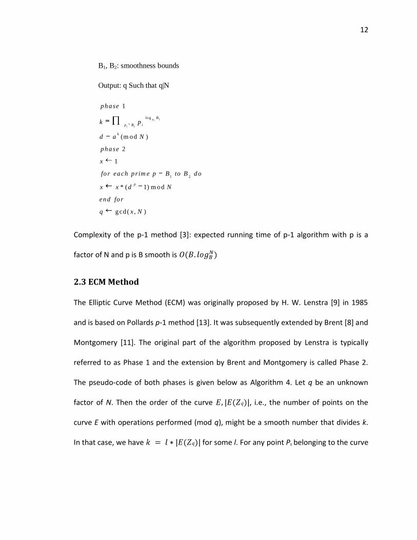
Complexity of the p-1 method [3]: expected running time of p-1 algorithm with p is a
factor of N and p is B smooth is
2.3 ECM Method
The Elliptic Curve Method (ECM) was originally proposed by H. W. Lenstra [9] in 1985
and is based on Pollards p-1 method [13]. It was subsequently extended by Brent [8] and
Montgomery [11]. The original part of the algorithm proposed by Lenstra is typically
referred to as Phase 1 and the extension by Brent and Montgomery is called Phase 2.
The pseudo-code of both phases is given below as Algorithm 4. Let q be an unknown
factor of N. Then the order of the curve , i.e., the number of points on the
curve E with operations performed (mod q), might be a smooth number that divides k.
In that case, we have for some l. For any point P0 belonging to the curve

13
, therefore . Thus, , and
the unknown factor of , can be recovered by taking .
Montgomery and Brent independently suggested a continuation of Phase 1 if one has
kP0 ≠ O. Their ideas utilize the fact that even if one has Q0 = kP0 ≠ O, the value of k might
miss just one large prime divisor of |E(Zq)|. In that case, one only needs to compute the
scalar multiplication by p to get pQ0 = O. A second bound B2 restricts the size of possible
values of p.
Let be the cost of one multiplication (mod N). Then Phase 1 of ECM finds a factor
q of N with the conjectured time complexity O(exp((p2 + o(1))plog q log log q)M(N)) [9].
Phase 2 speeds up Lenstra's original method by the factor log q which is absorbed in the
term of the complexity, but is significant for small and medium size factors. More
details about ECM and the hardware implementation can be found in the Master’s
thesis presented by Khaleeluddin Mohammed [5].
Algorithm 4: ECM Algorithm
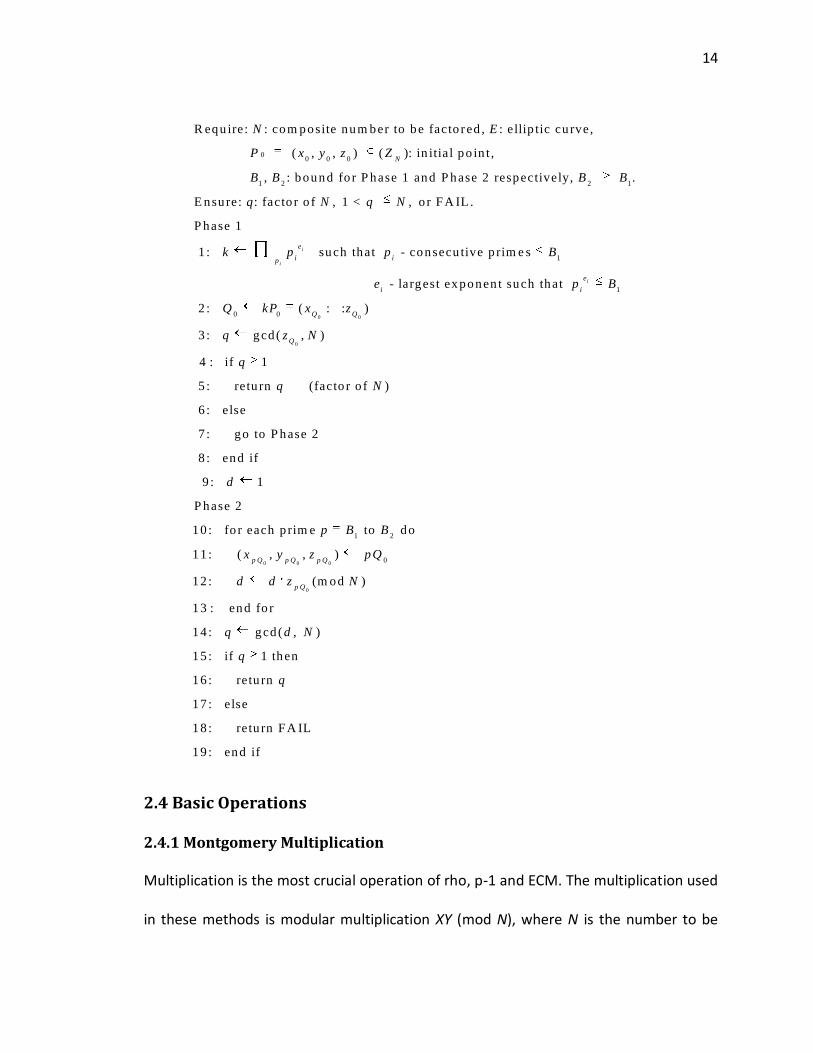
14
00 0 0
1 2 2 1
R equ ire: : com posite num ber to be facto r ed , : e llip tic cu rve,
( , , ) ( ): in itia l po in t ,
, : bound fo r P hase 1 and P hase 2 respectively, .
E nsu re:
N
N E
P x y z Z
B B B B
0
1
1
0 0
: facto r o f , 1 < , o r F A IL .
P hase 1
1 : such that - consecu tive p rim e s
- largest exponen t such that
2 : ( :
i
i
i
e
i ip
e
i i
Q
q N q N
k p p B
e p B
Q kP x0
0
0 0 0
1 2
0
: )
3 : gcd ( , )
4 : if 1
5 : re tu rn (facto r o f )
6 : e lse
7 : go to P hase 2
8 : end if
9 : 1
P hase 2
10 : fo r each p rim e to do
11 : ( , , )
12 :
Q
Q
p Q p Q p Q
z
q z N
q
q N
d
p B B
x y z pQ
0
(m od )
13 : end fo r
14 : gcd ( , )
15 : if 1 then
16 : re tu rn
17 : e lse
18 : re tu rn F A IL
19 : end if
p Qd d z N
q d N
q
q
2.4 Basic Operations
2.4.1 Montgomery Multiplication
Multiplication is the most crucial operation of rho, p-1 and ECM. The multiplication used
in these methods is modular multiplication XY (mod N), where N is the number to be
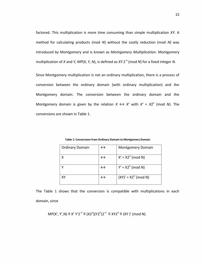
15
factored. This multiplication is more time consuming than simple multiplication XY. A
method for calculating products (mod N) without the costly reduction (mod N) was
introduced by Montgomery and is known as Montgomery Multiplication. Montgomery
multiplication of X and Y, MP(X, Y, N), is defined as XY 2-n (mod N) for a fixed integer N.
Since Montgomery multiplication is not an ordinary multiplication, there is a process of
conversion between the ordinary domain (with ordinary multiplication) and the
Montgomery domain. The conversion between the ordinary domain and the
Montgomery domain is given by the relation X ↔ X’ with X’ = X2n (mod N). The
conversions are shown in Table 1.
Table 1: Conversions from Ordinary Domain to Montgomery Domain
Ordinary Domain ↔ Montgomery Domain
X ↔ X’ = X2n (mod N)
Y ↔ Y’ = X2n (mod N)
XY ↔ (XY)’ = X2n (mod N)
The Table 1 shows that the conversion is compatible with multiplications in each
domain, since
MP(X’, Y’,N) ≡ X’ Y’2-n ≡ (X2n)(Y2n)2-n ≡ XY2n ≡ (XY )’ (mod N).
16
The conversion between each domain can be done using the same Montgomery
operation, in particular X’ = MP(X, 22n(modN), N) and X = MP(X’,1,N), where 22n(modN)
can be pre-computed. Despite the initial conversion cost, as many Montgomery
multiplications are followed by a single conversion, an advantage over ordinary
multiplication is obtained.
The pseudo-code for radix-2 Montgomery multiplication is shown in Algorithm 3 where
2log 2n N . It should be mentioned that here n is slightly different from
2log 1N which Montgomery [10] originally used. This modified algorithm makes all
the inputs and output in the same range, i.e., 0 ≤ X, Y, S[n] < 2N. Therefore it is possible
to implement Algorithm 5 repeatedly without any reduction unlike the original
algorithm [10], where one has to take reduction (mod N) at the end of the algorithm to
make the output value in the same range as the input values.
2.4.2 Exponentiation Algorithms
The main part of the p-1 algorithm is based on exponentiation. Given a number g, and
exponent the result is ge. There are many algorithms for modular exponentiation. Some
of the methods are left to right binary exponentiation, right to left binary
exponentiation, exponentiation using addition chains, window based exponentiation
method etc. Out of several algorithms described in [3], we have selected sliding window
exponentiation as best suited for the hardware implementation of exponentiation in the
p-1 method. This algorithm is described as Algorithm 6.
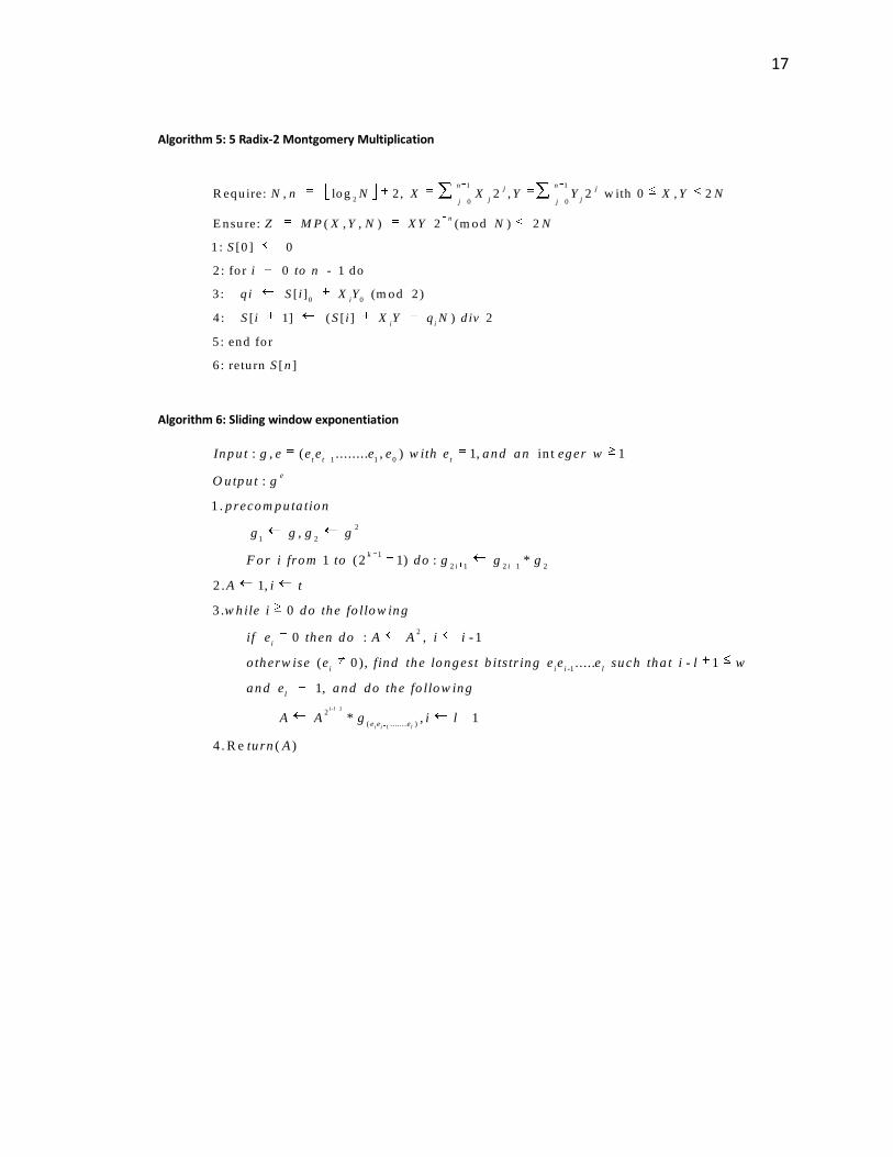
17
Algorithm 5: 5 Radix-2 Montgomery Multiplication
1 1
2 0 0
0 0
R equ ire: , log 2, 2 , 2 w ith 0 , 2
E nsure: ( , , ) 2 (m od ) 2
1 : [0 ] 0
2 : fo r 0 - 1 do
3 : [ ] (m od 2 )
4 : [ 1] ( [ ]
n nj j
j jj j
n
i
N n N X X Y Y X Y N
Z M P X Y N X Y N N
S
i to n
q i S i X Y
S i S i ) 2
5 : end fo r
6 : retu rn [ ]
i iX Y q N div
S n
Algorithm 6: Sliding window exponentiation
1 1 0
2
1 2
1
2 1 2 1 2
: , ( ........ , ) 1, in t 1
:
1 .
,
1 (2 1) : *
2 . 1,
3 . 0
t t t
e
k
i i
Inpu t g e e e e e w ith e a n d a n eger w
O utpu t g
precom pu ta tion
g g g g
F or i from to do g g g
A i t
w h ile i do the fo llow ing
i
- 1
1
2
-1
2
( ....... )
0 : , - 1
( 0 ), ..... - 1
1,
* , 1i l
i i l
i
i i i l
l
e e e
f e then do A A i i
o therw ise e fin d th e longest b its tr ing e e e such tha t i l w
and e and do the fo llo w in g
A A g i l
4 . R e ( )tu rn A
18
Chapter 3: Proposed architecture of co-factoring circuit
Proposed architecture of the co-factoring circuit will perform all the three algorithms
starting with rho, p-1 and finally ECM. In ASIC implementation, unifying all three
algorithms reduces the non-recurrent cost, as only one instead of three devices needs to
be developed and fabricated. Each device can perform all three functions, which
increases flexibility while building and reusing a large factoring circuit.
In FPGA implementation, these issues are not of primary concern, as non-recurrent
costs are minimal and devices can be reconfigured in the middle of computations. In
both types of implementations, transfer of inputs and outputs between hardware
devices can be reduced in the unified architecture. Another reason for unification of p-1
and ECM is that these methods make use of the same parameters such as the product
of prime powers that are less than B1, gcd tables and prime tables. With minor
modifications all this data can be used for both methods.
Original idea was to unify all the three special methods of factoring rho, p-1 and ECM.
But due to time limitation and design discrepancies only unification of rho and p-1 has
been completed. ECM method of factoring is implemented using two multipliers and

19
one adder/subtractor whereas rho and p-1 are implemented using only one multiplier
and one adder/subtractor. Unification of all three methods requires implementation of
ECM using only one multiplier and one adder/subtractor, which would require a very
substantial amount of time and effort. That’s why only the unification of rho and p-1 is
done, leaving unification of ECM as future work.
3.1 Top Level View
Figure 3: Proposed architecture for co-factoring
Proposed architecture of the co-factoring is shown in Figure 3. In this circuit, host
computer is responsible for pre computations such as computing the initial parameters
Control
Unit
Global
memory
I/O
FPGA / ASIC
RAM
Host
computer
Co-factoring Units
Instruction
ROM
20
needed for all the three algorithms, and post computations such as calculating gcd of
the result from the algorithms with the number to be factored. It is also responsible for
transferring the initial parameters needed to the global memory. This architecture has
multiple co-factoring units performing the similar algorithms in parallel on the same or
different numbers, using different sets of parameters. Operation of the units is
controlled by a global control unit. The control unit monitors and controls the operation
of the whole circuit. Details about the contents of the global memory for ECM, the
architecture of ECM unit were explained in the thesis submitted by Khaleeluddin
Mohammed. Details of the remaining units, i.e., rho, p-1 and the unified rho and p-1 are
explained in Section 4.
3.2 Implementation of Basic Arithmetic Operations
Low level arithmetic unit is the same for all the three architectures. This arithmetic unit
has one Montgomery multiplier and one adder/subtractor. Three basic low level
operations of the rho, p-1 and unified rho and p-1 are modular multiplication (defined in
section 2.4.1), modular addition and modular subtraction. Modular addition and
subtraction are very similar to each other, and as a result they are implemented using
one functional unit, adder/subtractor.
In order to simplify our Montgomery multiplier, all operations are performed on inputs
X; Y in the range 0 ≤ X, Y < 2N, and return an output S in the same range, 0 ≤ S < 2N. This
is equivalent to computing all intermediate results modulo 2N instead of N, which

21
increases the size of all intermediate values by one bit, but shortens the time of
computations, and leads to exactly the same final results as operations (mod N).
3.2.1 Modular Addition and Subtraction
The algorithms for modular addition and subtraction are shown as Algorithms 7 and 8
respectively. In both algorithms, S is the result, T is the temporary variable and C1, C2
are two carry bits. The block diagram of the adder/subtractor unit implementing both
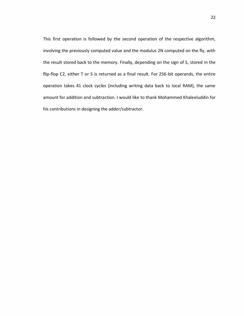
algorithms are shown in Figure 4. The modulus N is loaded to the adder/subtractor,
using input X_N, one time, during the initialization stage of Phase 1 using the control
signal X_N_Choice given by the control unit, and does not need to be changed until the
next run of Phase 1 for another number N. This modulus is stored in the internal 32x32-
bit memory, used to hold three numbers N, S, and T, all up to 256 bits wide. The 32-bit
words of operands X and Y are loaded in parallel, starting from the least significant
word, and immediately added or subtracted, depending on the value of the control
input sub (with sub = 1 denoting subtraction). The result is stored in the internal
memory as a variable T for addition, i.e., X + Y, and S for subtraction, i.e., X - Y. Here
subtraction is nothing but addition in 2's compliment, which is done by inverting one of
the inputs, done by the XOR gates at the input of the adder and by setting the carry bit
C2, these operations are controlled the sub signal coming from the adder/subtractor
state machine
22
This first operation is followed by the second operation of the respective algorithm,
involving the previously computed value and the modulus 2N computed on the fly, with
the result stored back to the memory. Finally, depending on the sign of S, stored in the
flip-flop C2, either T or S is returned as a final result. For 256-bit operands, the entire
operation takes 41 clock cycles (including writing data back to local RAM), the same
amount for addition and subtraction. I would like to thank Mohammed Khaleeluddin for
his contributions in designing the adder/subtractor.
23
+
C 1
C 2
L U T
3 2 X 3 2
M E M
<>
ad d r1 ad d r2W E L
O P 1 O P 2
X _ N _ C h oice
X _ N Y
su b
s ig n Z
read
C inC ou t
su m 1 su m 2E C 1
E C 2
X _ N
A D D E R
3 2 b ti reg X 3 2 b ti reg Y
E YE X
N
2 N
<<1
Figure 4: Block diagram of the adder/subtractor

24
Algorithm 7: Modular Addition
( ) ( ) ( )
( ) ( ) ( )
1 1
R e : , , 2 , exp sin 32 - , , , , 0 , ...., - 1
: m od 2
1 : 0 - 1
2 : ( , )
3 :
4 : 0 - 1
5 :
j j j
j j j
qu ire N X Y N all ressed u g e b it w ords X Y N j e
E nsure Z X Y N
for j to e do
C T C X Y
end for
for j to e do
( ) ( ) ( )
2 2 ( , ) - (2 )
6 :
7 : 0
8 :
9 :
10 :
11 :
j j jC S C T N
end for
if S then
return T
else
return S
end if
Algorithm 8: Modular Subtraction
( ) ( ) ( )
( ) ( ) ( )
2 2
R e : , , 2 , exp sin 32 -
, , , 0 , ....., - 1
: - m od 2
1 : 0 - 1
2 : ( , ) -
3 :
4 : 0
j j j
j j j
qu ire N X Y N all ressed u g e b it w ords
X Y N j e
E nsure Z X Y N
for j to e do
C S C X Y
end for
fo r j to e
( ) ( ) ( )
1 1
- 1
5 : ( , ) (2 )
6 :
7 : 0
8 :
9 :
10 :
11 :
j j j
do
C T C S N
end for
if S then
return T
else
return S
end if
3.2.2 Montgomery Multiplier
The multiplier circuit used was designed by my colleague Hoang Le. This multiplier is
based on the radix-2 version of the Montgomery Multiplier algorithm shown in
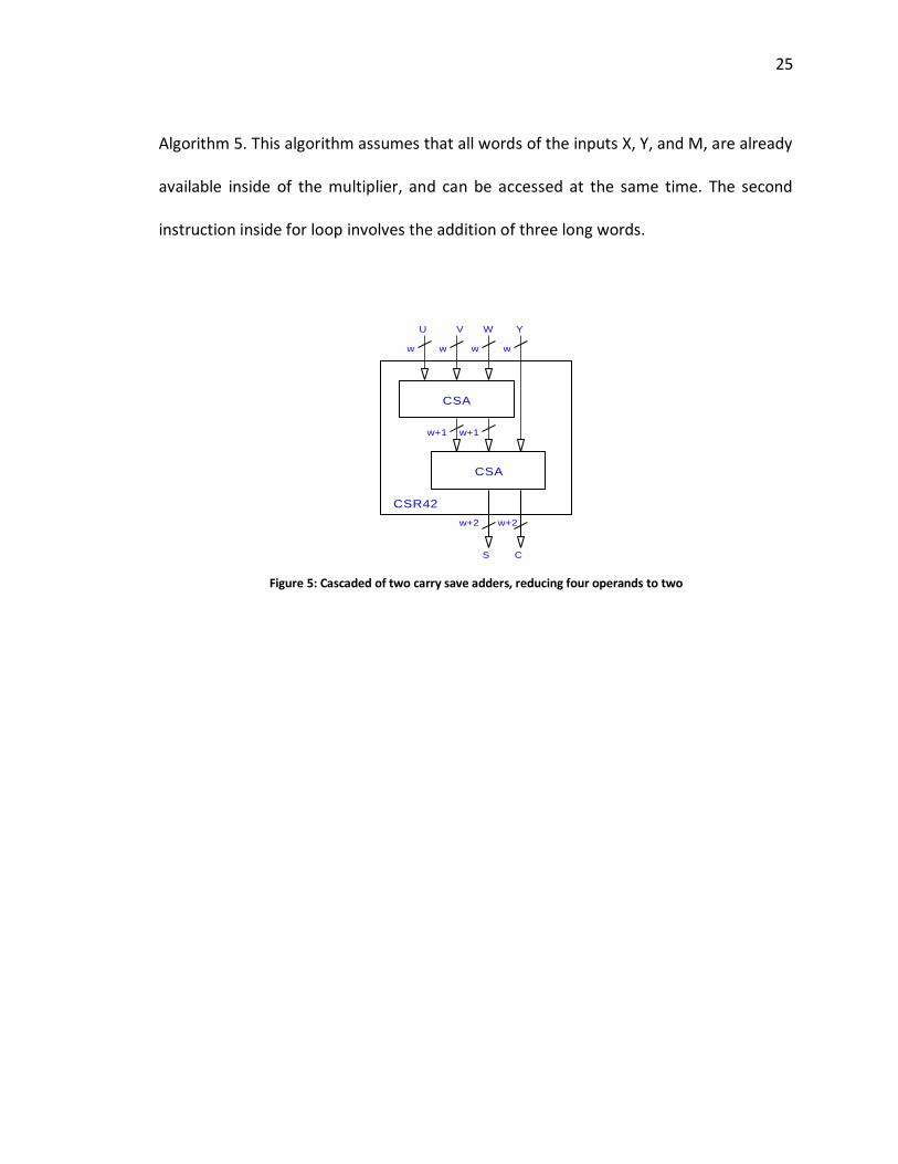
25
Algorithm 5. This algorithm assumes that all words of the inputs X, Y, and M, are already
available inside of the multiplier, and can be accessed at the same time. The second
instruction inside for loop involves the addition of three long words.
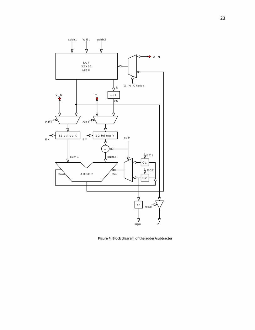
Figure 5: Cascaded of two carry save adders, reducing four operands to two
VU W Y
CSA
CSA
S C
CSR42
w w w w
w+1 w+1
w+2 w+2
26
S 1 S 2
A (S h ift_R eg)
B
C S R 42
> > 1
> > 1
S 1in S 2 in
A
B
zeros zeros
n
n nB B
S 1out S 2out B out
c arrys um
S 1in
S 2 in
A N D
S 2out(0 )
S 1out(0 )
B ou t(0 )
A i
A i q i
A 1 A 2 B C
S U M C A R R Y
E s E s
loadA
E b
reg _ rs t reg _ rs t
res et
res et
S S 1
E s s
res et S S 2
E s s
res et
S 1out S 2out
q i
n
nout
E b
res et
A i
A (0 )
Figure 6: Block diagram of the multiplier
If implemented directly in hardware the operation would result in a long critical path
and a very low clock frequency. In order to prevent that, this addition is performed
using carry save adders, and the result S [i + 1] is stored in the carry save form. Using
carry save adders, the sum of three numbers U, V , W is reduced to the sum of two
numbers S (sum) and C (carry), such that U + V + W = C + S. Similarly, using a cascade of
two carry save adders, as shown in Figure 5, the sum of four numbers, U, V , W, and Y
can be reduced to the sum of two numbers S and C, such that U +V +W +Y = C +S. Each
carry save adder is composed of a row of n Full Adders working in parallel, so it
27
introduces a delay of just a single Full Adder (i.e., a delay of a single stage of a basic
ripple-carry adder). The modified algorithm, based on carry save addition (CSA) is shown
as Algorithm 9. This algorithm has been described earlier in. This block diagram of the
circuit implementing Algorithm 9 is shown in Figure 6. The modulus N and the
parameter n are loaded in to the multiplier once at the beginning of Phase 1, and do not
need to be changed until the beginning of Phase 1 for another number N. At the
beginning of multiplication, the inputs X and Y are first loaded in parallel, in 32-bit
words, to internal 256-bit registers X and Y. In the following n clock cycles, the circuit
executes n iterations of for loop. Finally, in the last 8 clock cycles, the final result is
computed word by word, starting from the least significant word, and transferred to the
output. The total execution time of a single Montgomery multiplication is equal to n +
16 clock cycles.

28
Algorithm 9: Radix-2 Montgomery Multiplication with carry save addition
-1
2 0
- ( ) ( ) ( )
R equ ire: , log 2, 2 w ith 0 , 2
E nsure: ( , , ) 2 (m od ) 2 ; , [ ] , [ ] deno te a
j-th w ord o f , [ ] and [ ] res pectively.
1 : [0 ] 0
2 : [0 ] 0
3 : fo
n j
jj
n j j j
N n N X X X Y N
Z M P X Y N X Y N N Z C n S n
Z C n S n
S
C
0 0 0
( ) ( ) ( )
( )
r 0 - 1 do
4 : ( [ ] [ ] ) (m od 2)
5 : ( [ 1], [ 1]) ( [ ], [ ], , ) 2
6 : end fo r
7 : 0
8 : fo r 0 to 7 do
9 : ( , ) [ ] [ ]
10 : retu rn
11 : end fo r
i i
i
j j j
j
i to n
q C i S i X Y
C i S i C SA C i S i X i Y q N div
C
j
C Z C n S n C
Z
29
Chapter 4: Architecture of Rho and p-1
4.1 Partitioning of operations between hardware and software
All the computations in three architectures can be divided into three categories, pre-
computations, main computations and post-computations. Pre-computations and post-
computations are performed using the host computer, whereas main computations are
performed in hardware. In a typical scenario, the pre and post computations take
negligible amount of time when compared to the time taken for main computations in
hardware.
For rho method pre-computations are converting the initial point and other parameters
needed for the algorithm to Montgomery domain, and the main computations are
executing the Algorithm 10 which involves in Montgomery multiplication and
Montgomery addition and subtraction.
The software pre-computation for phase1 of p-1 include calculating product of power of
primes k, which is dependent on B1, and converting initial values needed for algorithm
execution, i.e., a and g, into the Montgomery domain. The phase 2 pre-computations
30
include the generation of two bit tables, prime_table and GCD_table, described in
Section 4.2.
These bit tables can be re-used for most of the time as long as boundaries B1 and B2 are
kept constant. Thus, these values need to be calculated only once, if we use the same
bounds. Main computations in hardware for p-1 include modular exponentiation, and
phase 2 operations, modular multiplication and modular subtraction, which will be
running most of the time. These main computations done in hardware will be keeping
majority of hardware resources busy almost all the time.
For the unified architecture, pre-computations are combination of pre-computations
from individual rho and p-1 units. The main computations are also combination of
individual rho and p-1 operations.
In all three architectures, post-computations consist of calculating the gcd of the final
results with the number to be factored, which is done in the end and done only once.
Top level block diagram of the three architectures looks similar and the difference will
be explained in the following sections.
In all the three architectures multiple identical units will be working in parallel on the
same or different numbers with different sets of parameters depending on the
requirement. Each unit has its own local memory, Montgomery multiplier and
adder/subtractor. Global memory, instruction memory and control unit are common for

31
all processing units. The operation starts with loading the initial parameters needed by
the particular architecture. Once all the computations are finished in hardware, the
result is transferred to host pc for final gcd calculation.
U N IT 1
A /S
M U L
L O C A L
M E M
U N IT n
A /S
M U L
L O C A L
M E M
C O N TR O L
U N IT
G L O B A L
M E M
Figure 7: Top level block diagram
As the contents of the global memory are different for different factoring methods, they
are explained in detail with the block diagrams in this section.
In this sections hardware architectures of all the three implementations, i.e., rho, p-1
and unified rho and p-1 are discussed in detail. Along with the architecture, the
32
optimization criteria and the criteria for selecting optimum number of arithmetic units
are also discussed.
4.2 Hardware Architecture of Rho Method
The Algorithm 1, which was explained in Section 2.1, can be re-written as shown in
Algorithm 10, clearly defining all the inputs, outputs of the system and the complete
execution of the algorithm.
Algorithm 10: Re-written rho algorithm based on Algorithm 1
2
0
1 1 0 2 2 1 2 1 2 1
2
2 2
2 2
2
2 2
2 2
2
1 1
1 1
: , , ( ) , , ( , 2 )
: ( | )
( ), ( ), - - , 1
( 2; ; )
{
*
Inpu ts x a f x x a N t even
O utpu ts q such tha t q N
v x f x v x f x tem p v v x x d
for i i t i
v v
v v a
v v
v v a
v v
v v a a ll opera tions are done
tem2 1
- m od
*
}
gcd ( , )
p v v u lo N
d d tem p
q d N
As explained in Section 2.1, in order to minimize the number of gcd computations, we
are trying to accumulate the differences between the numbers of the sequence x i
wherever the difference between the indices increases by one. This increase comes
from applying the polynomial twice to x2i and once to xi. This scheme results in a regular
33
pattern of the numbers, where the difference between the indices of the numbers is
increased by one in each iteration. The reason for increasing the differences in indices
by one is to find out the loop length starting from 1 till it occurs. If we collect the value
of every difference, one of the differences leads to a factor of N. The corresponding
graphical representation of the above explained Algorithm 10 is shown in Figure 7.
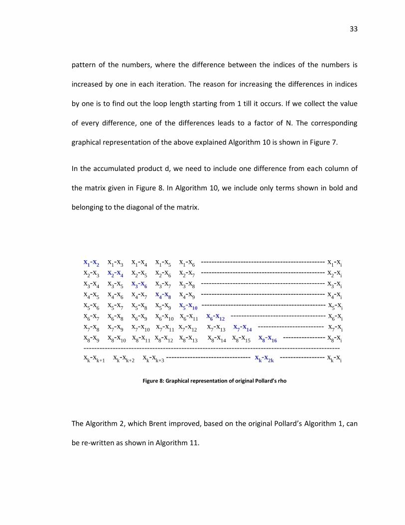
In the accumulated product d, we need to include one difference from each column of
the matrix given in Figure 8. In Algorithm 10, we include only terms shown in bold and
belonging to the diagonal of the matrix.
Figure 8: Graphical representation of original Pollard’s rho
The Algorithm 2, which Brent improved, based on the original Pollard’s Algorithm 1, can
be re-written as shown in Algorithm 11.
x1-x
2 x
1-x
3 x
1-x
4 x
1-x
5 x
1-x
6 ----------------------------------------------- x
1-x
i
x2-x
3 x
2-x
4 x
2-x
5 x
2-x
6 x
2-x
7 ----------------------------------------------- x
2-x
i
x3-x
4 x
3-x
5 x
3-x
6 x
3-x
7 x
3-x
8 ----------------------------------------------- x
3-x
i
x4-x
5 x
4-x
6 x
4-x
7 x
4-x
8 x
4-x
9 ----------------------------------------------- x
4-x
i
x5-x
6 x5-x
7 x
5-x
8 x
5-x
9 x
5-x
10 ----------------------------------------------- x
5-x
i
x6-x
7 x
6-x
8 x
6-x
9 x
6-x
10 x
6-x
11 x
6-x
12 ------------------------------------ x
6-x
i
x7-x
8 x
7-x
9 x
7-x
10 x
7-x
11 x
7-x
12 x
7-x
13 x
7-x
14 ------------------------- x
7-x
i
x8-x
9 x
8-x
10 x
8-x
11 x
8-x
12 x
8-x
13 x
8-x
14 x
8-x
15 x8-x
16 ---------------- x
8-x
i
-------------------------------------------------------------------------------------------------
xk-x
k+1 x
k-x
k+2 x
k-x
k+3 -------------------------------- xk
-x2k ----------------- xk
-xi
34
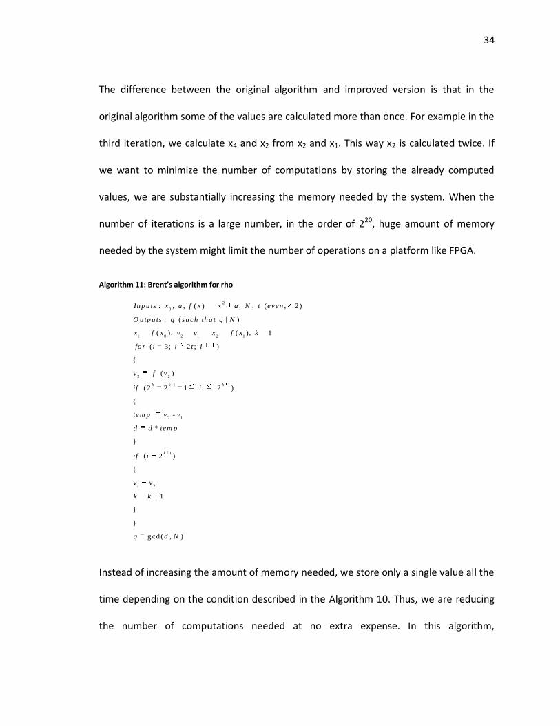
The difference between the original algorithm and improved version is that in the
original algorithm some of the values are calculated more than once. For example in the
third iteration, we calculate x4 and x2 from x2 and x1. This way x2 is calculated twice. If
we want to minimize the number of computations by storing the already computed
values, we are substantially increasing the memory needed by the system. When the
number of iterations is a large number, in the order of 220, huge amount of memory
needed by the system might limit the number of operations on a platform like FPGA.
Algorithm 11: Brent’s algorithm for rho
2
0
1 0 2 1 2 1
2 2
-1 1
2 1
1
1 2
: , , ( ) , , ( , 2 )
: ( | )
( ), ( ), 1
( 3; 2 ; )
{
( )
(2 2 1 2 )
{
-
*
}
( 2 )
{
1
}
}
g
k k k
k
In p u ts x a f x x a N t even
O u tp u ts q su ch th a t q N
x f x v v x f x k
fo r i i t i
v f v
if i
tem p v v
d d tem p
if i
v v
k k
q cd ( , )d N
Instead of increasing the amount of memory needed, we store only a single value all the
time depending on the condition described in the Algorithm 10. Thus, we are reducing
the number of computations needed at no extra expense. In this algorithm,

35
accumulation is not performed in every iteration as in the Algorithm 10, even though
the number of the accumulations is the same in both methods. The corresponding
graphical representation of Algorithm 11 is shown in Figure 9.
In this method whenever the iteration number is equal to power of two, the
corresponding value of x will be stored and depending on the condition explained in the
Algorithm 11, the appropriate difference and the accumulation will be computed.
Similarities between the two methods are as follows: In each method there is an
element (difference between two values) from each column contributing to the final
accumulated product. The differences between the indices cover all the values from 1
till the iteration value, which makes both methods equivalent.
Figure 9: Graphical representation of improved version by Brent
x1-x
2 x
1-x
3 x
1-x
4 x
1-x
5 x
1-x
6 ---------------------------------------------------- x
1-x
i
x2-x
3 x
2-x
4 x
2-x
5 x
2-x
6 x
2-x
7 ---------------------------------------------------- x
2-x
i
x3-x
4 x
3-x
5 x
3-x
6 x
3-x
7 x
3-x
8 ---------------------------------------------------- x
3-x
i
x4-x
5 x
4-x
6 x
4-x
7 x
4-x
8 x
4-x
9 ---------------------------------------------------- x
4-x
i
x5-x
6 x5-x
7 x
5-x
8 x
5-x
9 x
5-x
10 ----------------------------------------------------- x
5-x
i
x6-x
7 x
6-x
8 x
6-x
9 x
6-x
10 x
6-x
11 x
6-x
12 ------------------------------------------ x
6-x
i
x7-x
8 x
7-x
9 x
7-x
10 x
7-x
11 x
7-x
12 x
7-x
13 x
7-x
14 ------------------------- ------ x
7-x
i
x8-x
9 x
8-x
10 x
8-x
11 x
8-x
12 x
8-x
13 x
8-x
14 x
8-x
15 x8-x
16 ---------------------- x
8-x
i
--------------------------------------------------------------------------------------------------------
xk-x
k+1 x
k-x
k+2 x
k-x
k+3 ----------------x(2
k) – x(2k
+ 2k-1
+1) ------------- x(2k)-x(2
k+1)----- xk-xi

36
Speed up vs. Original Pollard’s rho:
Number of operations in terms of multiplications, additions and subtractions for arriving
at x8-x16 for both methods are as follows:
Pollard’s algorithm:
Number of multiplications: 30
Number of additions: 23
Number of subtractions: 8
Brent’s algorithm:
Number of multiplications: 23
Number of additions: 16
Number of subtractions: 8
For the above case, and in general, Brent’s algorithm is approximately 25% faster than
Pollard’s algorithm, and thus Brent’s algorithm is chosen for hardware implementation.

37
Figure 10: Sequence of operations in hardware for Brent’s rho
Operation table in hardware:
Inputs: x0, a, f(x) =x
2
+a, n, t (even,>2)
Outputs: d
Table 2: Operation table for rho
MUL ADD/SUB
1 to 2t-1 v
2 ← v
2
2
cond1 temp ← (v
2-v
1)
cond1 d ← d*temp 1 to 2t-1 v2
← v2+ a
cond1: 2k
+2k-1
+1≤ i-1 ≤2k+1
v2 d v
1
x2 d=1 x
2
x3
x4 d=d*(x
4-x
2) x4
x5
x6
x7 d*(x
7-x
4)
x8 d*(x
8-x
4) x
8
x9
x10
x11
x12
x13 d*(x
13-x
8)
x14 d*(x
14-x
8)
x15 d*(x
15-x
8)
x16 d*(x
16-x
8) x
16

38
The sequence of operations in hardware is shown in Figure 10. As already explained,
whenever the index of v2 is a power of two, it is stored in v1 and used for subtractions
later. In selecting the number of arithmetic units, Table 2 is taken into account. In all the
operations, subtraction and accumulation are done only when the condition is satisfied.
As the algorithm checks for a specific condition, which is not all the time true, the
operations cannot be effectively parallelized, as there are dependencies among the
computations. If we have more than one multiplier and adder/subtractor, only one
multiplier and one adder/subtractor are active all the time and the other pair of
arithmetic units will be in use for less than 50% of the time, in which case the resources
are not utilized efficiently. This criterion justifies the selection of one multiplier and one
adder/subtractor for the implementation.
4.3 Hardware Architecture of P-1 Method
The Algorithm 2, which was explained as a part of overview of p-1 will be explained in
detail in this section. The Algorithm 3 can be described as two phases, and the Phase 1 is
shown in Algorithm 12.
Algorithm 12: Phase1 of p-1 algorithm
Inputs:

39
The primary operation of Phase 1 is modular exponentiation. Value of the exponent k
used in the exponentiation is independent of n and can be pre-computed. Out of
multiple algorithms existing for modular exponentiation, sliding window method has
been selected for phase 1. Based on the number of operations to finish the
exponentiation addition chain method is the fastest one, but it requires a lot of memory
resources which would limit the number of processing units that can be placed on low-
cost FPGAs. On the other hand, if we choose one of the basic binary exponentiations, for
a random L-bit exponent, total number of multiplications will be 3*L/2 (assuming in a
randomly chosen number there are 50% bits of value ‘1’) which is more than the sliding
window method takes. Thus, the sliding window method is faster than binary
exponentiation, and needs less memory resources than addition chain method.
In case Phase 1 doesn’t produce a non-trivial factor of n, Phase 2 described in Algorithm
13 is applied. For the purpose of efficient hardware implementation, Algorithm 3 is
modified as follow.
Choose 0 < D <B2, and let every prime p, B1 < p ≤ B2, be expressed in the form
where m changes between MMIN = (B1 + D – 1)/D to MMAX = (B2 + 1) /
D , and j varies between 1 and D. The condition that p is prime implies that gcd(j, D) = 1.

40
Thus, possible values of j form a set Js = ,j: 1≤ j < D, gcd(j, D) = 1-, and the possible value
of m form a set MT = {m: MMIN ≤ m ≤ MMAX} of the size MN = MMAX – MMIN + 1, where MN
is approximately equal to (B2-B1)/D.
Then, the condition is satisfied, which implies
For this purpose, all values are pre-computed once Phase 2 is started. One then
computes with a current value of , and all pre-computed values, for which
is a prime. In order to simplify calculations, a bit table, prime_table is pre-
computed. when is a prime, and 0 otherwise. This
table can be reused for multiple iterations of Phase 2 with the same values of and .
Similarly another bit table GCD_table can be pre-computed.
when , and 0 otherwise
This table will have bits and this leads to the phase 2 algorithm shown in Algorithm
13. Value of is the most natural choice for D as it minimizes the
size of set JS and as a result of the amount of pre-computations and memory storage
required for phase 2.

41
Algorithm 13: Phase 2 of p-1 algorithm
m in 1 m ax 2
m in m ax
( ) / , ( - 1) /
_
1 - 1
g cd ( , ) 1
_ [ ] 1
_
1 - 1
M B D D M B D D
clear G C D tab le
fo r each j to D do
if j D then
G C D tab le j
end if
end fo r
clear p rim e tab le
fo r each m M to M do
for ea ch j to D
*
m in
( * - )
_ [ , ] 1
1 - 1
(gcd ( , )) 1
1, ,
j
m D D
if m D j is p rim e then
prim e tab le m j
end if
end fo r
end fo r
fo r each j to D do
if j D then
com pu te d
end if
end fo r
x y d t d
fo r m M tm ax
1 - 1
( _ [ , ] 1)
* ( - )
*
g cd ( , )
j
o M
for j to D
if p rim e tab le m j
x x y d
en d if
end fo r
y y t
end fo r
q x N
4.4 Global Memory Maps
4.4.1 Rho

42
Figure 11: Contents of global memory for rho
Global memory is a single port memory. It transfers data to and from local memories
word by word. Prior to the execution of the algorithm, host pc transfers the data to
global memory. The memory map of the global memory is shown in the Figure 11. This
includes the data needed by each unit to start the execution of the algorithm, such as
modulus n, initial point x0, and a small integer a. It also contains the number of
n for unit1
n for unit2
x0
a
. . .
31 0 0
t
n for unit m
. . .
No. of iterations
Same for all units

43
iterations t needed by the control unit to determine the end of the execution. All the
parameters needed by each unit will be transferred and then the computations will be
started.
Once all the computations are finished, the results from all the units will be transferred
to the global memory, which sends all that data to host pc for gcd calculation. In the p-1
method global memory is responsible for holding the data, which is needed for phase1
and phase2. The contents of the global memory in Phase 1 and 2 is shown in Figure 12
4.4.2 P-1
Figure 12: Contents of global memory for p-1 a) phase 1 b) phase 2
511
prime_table[1]
GCD_table[1]
GCD_table[GMAXD]
Mmin
Mmax
31 0 0
. . .
prime_table[2]
. . .
prime_table[PMAXD]
Phase2
Determines j such that
1 ≤ j ≤ D and
gcd(j, D) = 1
Determines m, j such
that p=m·D - j is prime
Phase 1
n for unit1
k
n for unit2
g2
g1
. .
. initial values
for
all units
kN
31 0 0
511
n for unit m
b) a)
44
Parameters needed for p-1 algorithm
n, the number to be factored
a, small integer where gcd (a, n) = 1
k, product of prime powers which are less than B1
gcd and prime tables needed for phase2.
4.4.3 Unified rho and p-1
Contents of the global memory of unified rho and p-1 are combination of both rho and
p-1 global memory contents. Only difference here is once rho algorithm is completed,
instead of computing gcd, it continues with p-1 algorithm and once the execution of two
algorithms is finished, then the result from both the units will be transferred to global
memory. These results will then be sent to host computer for gcd computations. All the
global and local memory requirements for all the three architectures are specified in the
Results section.
4.4 Local Memory Maps
4.4.1 Medium level operations
In rho the medium level operations are computing the value of v2 and computing the
accumulated product d, based on the iteration value. The final value of d is computed
using the condition specified in Table 2.
45
Medium level operations in p-1 algorithm are modular exponentiation in phase 1 and
finding the value of x in phase 2. In phase 1, exponentiation is performed using sliding
window exponentiation based on the value of k, which depends on the phase 1 bound
B1. In phase2, calculating the value of x is based on the GCD_table and prime_table.
In the unified rho and p-1 the medium level operations will be rho operation and p-1
operation. First the unit tries to factor the number using rho method, and once rho is
completed it moves into p-1 algorithm, so that if the number has more than one factor,
both factors will be given as output. The main advantages of integrating both rho and p-
1 are both units use the same low level unit, there is a possibility to find more than one
factor in a single run.
4.4.2 Rho
Local memory is a single port in and dual port out memory. The purpose of having dual
port out is to load the two operands simultaneously for multiplication, addition and
subtraction. Single port in is sufficient for loading data into the local memory from
global memory, multiplier and adder/subtractor. This local memory transfers the data to
global memory after all the computations are done using a tri-state buffer which
connects local memory to global memory. Contents of local memory are shown in the
Figure 13.

46
4.4.3 P-1
Local memory is a dual port in and dual port out memory. The reason for selecting dual
port memory is to ease the loading of both the operands simultaneously for addition,
subtraction and multiplication. It is also helpful if there is any data movement that
needs to be done within the local memory. This feature also supports data output to the
global memory once the whole algorithm has been executed. This is done using a tri
state buffer at port A.
M
tem p
V 1
V 2
a
d
L o ca l M e m o ry
0
63
031
6
6
32
A addr
B addr
W E A
A _M
B
32
32
32
G re i
da ta_out
0
01
1
g _ l
u_ l
K out
C
32
32
data_ in
Figure 13: Contents of local memory of rho

47
LO C A L
M E M O R Y
G R E i
D ata_ ou t
B
A _ M
C
A ad d r
W E A
W E B i
B ad d r
K ou t
A in
W E B
B in
A ad d r
B ad d r
W E A
A ou t
B ou t
3 1 0
0
5 1 1
3 2
3 2
3 2
3 2
9
2 0
9
3 2
sel_ d ata1
0
1
Figure 14: Local memory of p-1
The contents of the local memory in phase 1 and phase 2 are shown in Figure 15 (a) and
(b). In phase 1 it holds the modulus, and all the pre-computed values for sliding window
exponentiation and the result of phase1. In phase 2 it will hold values where
. It also has other values needed to compute the final result , which are
, and the difference between current and where is a prime.

48
Once all the operations are done, the result x which is at the last location of the local
memory will be transferred to global memory.
Figure 15: Contents of local memory of p-1 a) phase 1 b) phase 2
511
b)
g 2
31 0
0 N
g 1
d = g e
g 3
a)
Phase 1
. . . .
. . . .
g s
*s = 2k-1
d 2
31 0
0
511
N /d
d
d 11
d 13
d 209
Phase 2
. . . .
. . . .
d D
d m.D
d m.D - d j
x
49
4.4.4 Unified rho and p-1
Local memory of unified architecture will have two separate local memories. Once
memory is for holding the data needed and computed for rho and the other one for p-1.
Depending on the algorithm, the unit is accessing the corresponding local memory. All
the local memory requirements for the three architectures will be discussed in the
Results section.
4.5 Control Unit
Control units in all three architectures have been implemented in hardware. It is part of
the chip whether it is an FPGA or an ASIC. The basic components of the control units are
registers, shift registers, counters, flip flops, multiplexers and state machines. The
common operation among all the control units is, once host pc transfers the initial data
to global memory, control unit takes the control of the system and then it sends the
data to the individual units, and, once the whole algorithm is being executed, it transfers
the data to global memory. Finally the data are sent from global memory to host pc for
gcd calculation. The detailed operation of each control unit is explained as follow.
4.5.1 Rho
The control unit of rho has 5 state machines and a total of 45 states. The functions of
these state machines are transferring initial data required by the individual units, storing
the number of iterations in a register in the control unit, and executing the algorithm
50
based on the operation table described in Table 2. The detailed operation of the control
unit is described below.
Out of the four operations in the Table 2, and are performed all
the time irrespective of the condition in Table 2. Whereas the other operations
– and are performed only when the condition shown in
Table 2 is true. The flow of operations when the condition is true is as follows:
In the first row the multipliers are loaded with the two operands v2 and v2 which are the
same for the squaring operation, and multiplier is started. While the multiplier is
performing the squaring task, and from the previous iteration are transferred to
adder/subtractor for subtraction – operation, and the subtraction is done in
parallel with multiplication. Thus subtraction doesn’t need extra clock cycles to finish
the operation. In the second row addition is computed all the time.
When the condition is true the same strategy used for the first row of operations is
used. Multipliers are loaded with the operands needed for accumulation d and temp,
and the multiplication is started. The addition operation is done in parallel with the
multiplication, which effectively decreases the overall execution time.
Number of operations in rho with iterations is
First row
squarings for , t subtractions for
Second row
51
multiplications for accumulation
additions for
The total no. of operations is = (squaring + accumulation + *additions) = (
multiplications + * additions) as the remaining operations can be parallelized with the
multiplications. Once all the operations are completed, control unit transfers the data
from all the individual units to global memory which is the last operation of the control
unit.
4.5.2 P-1
The detailed operations performed by the control unit in p-1 are described in this
section. The control unit in p-1 has 12 state machines and total of 103 states. These
state machines execute Phase 1 and Phase 2 of the Algorithm. Sequence of operations
in Phase 1 is based on sliding window algorithm described in Algorithm 6.
Loading the initial values to all the individual units
Pre-computing all the odd powers of g used in the exponentiation
Computing the exponentiation as described in Algorithm 6. The window size is chosen as
5 and the control unit takes five bits from k, provided the first bit is not zero. If the first
bit is zero squaring operations are performed. After taking the 5 bits, the unit tries to
identify the window based on the condition that first and the last bits are non-zero.
Once the window size and the value are determined, squarings and the multiplication

52
with one of the pre-computed values are computed as described in the Algorithm 6.
Once all the bits of k are considered by the algorithm, Phase 1 is completed.
Sequence of operations in Phase 2 is based on the algorithm described in Algorithm 13.
The multiplier is loaded with d, result from Phase 1 for computing , which will be used
for computing values.
The next step is to compute the values based on GCD_table. The values are
computed for all the odd values of and only those values are stored for which
. This can be done with starting from d and multiplying the subsequent
values with .
The last value computed as part of the step is and for computing multiplier
is supplied with the operands and .
The next operation in sequence is computing from for . For this
operation as m is a small number, the left to right binary exponentiation [3] is used. The
result of this step is for .
The final operation of Phase 2 is accumulation based on the prime_table. For each pair
of , the prime_table has ‘1’ if is a prime and ‘0’ if it is not. If is a
prime, first the subtraction is calculated and then the multiplication is
performed with and as the operands and the result of this operation is

53
stored back in . This accumulation operation is performed for all the prime values in
the prime table.
If accumulation is finished for all the prime values of for a particular where
is a prime valued of is increased by one. It means multiplication is
computed and the value of is updated with the new value.
Once all the values are considered for accumulation Phase 2 algorithm is finished in
hardware and the result of Phase 2 is store in .
Control unit then transfers the result of Phase 2 to global memory which is the final step
of the p-1 algorithm.
4.5.3 Unified Unit
Control unit of unified unit performs combined operations from control units of
individual rho and p-1. It has 17 state machines and a total of 140 states for performing
the rho and p-1 operations in sequence.
Initially it loads the local memories for rho of individual units for the execution of rho.
Once rho algorithm is completely executed, it doesn’t transfer the result to global
memory as the control unit of rho does. Instead the control unit loads the initial values
and parameters needed for Phase 1 and Phase 2 of p-1 for the corresponding algorithm
execution. Once all the operations of p-1 are completed, control unit transfers results
from rho local memory and p-1 local memory to global memory. This is the final step of
the control unit for unified architecture.

54
Chapter 5: FPGA Implementation and Verification
5.1 Overview of FPGA families
An FPGA is a field programmable gate array with various configurable elements. The
user has the flexibility of re-configuring these devices based on the application. Xilinx
and Altera are the two main manufacturers of FPGAs and they hold a large market share
(around 89%). There are various families in Xilinx FPGAs based on the requirement and
application, i.e., technology, performance and cost.
The main families in the new Xilinx FPGAs are Virtex (high performance) and Spartan
(low cost). Some of the high performance FPGAs are
1. Virtex-II, Virtex-II pro based on 130 nm technology
2. Virtex-4 based on 90 nm technology
3. Virtex-5 based on 65 nm technology.
Out of the high performance FPGAs Virtex-5 is the most recent product which has lot of
DSP blocks embedded on it. Apart from Virtex-5, Virtex-4 is also used mostly in signal
processing applications. On the contrast Xilinx has low cost devices which are widely
used in most industrial applications. Some of the low cost FPGA families are

55
1. Spartan -3 based on 90 nm technology
2. Spartan-II derived from Virtex
3. Spartan-IIE derived from Virtex-E
Basic building blocks of Xilinx FPGA are CLB (Configurable Logic Block) slices. One CLB
slice has two Look Up Tables (LUTs) and two Flip Flops. Look Up Table is capable of
implementing any 4-input logic function. Apart from CLB slices depending on the
technology some of the FPGAs have power pc processors embedded, Ethernet mac
interface, multipliers and most of the Xilinx FPGAs have Block RAMs. These Block RAMs
are used whenever there is need to process or manage large amounts of data.
5.2 FPGA Design Flow
FPGA design flow is shown in Figure 16. It starts with design entry, in which the
specification will be analyzed and will be described in RTL using either VHDL or Verilog
HDL. It is done using block diagrams and ASM charts from the specification and these
will be developed to HDL. Once the RTL description is done, functionality should be
verified. It is verified using a testbench through functional simulation. This testbench
can further be used for other simulations also. If there are any discrepancies in the
design, we will go back to the design entry step and make some modifications in the RTL
description and then verify the functionality. Once the functionality is verified, next step
is to synthesize the code. Synplify pro is one of the best tools for synthesis. Synthesis is a
process where the RTL description will be converted to a gate level netlist. Once this
netlist is generated, we need to do the post-synthesis simulation to make sure that gate

56
level simulation is working properly. If there are any mis-matches in post-synthesis
simulation we need to go back to the RTL code and fix it before going to the process of
implementation. Once this simulation is verified next step is the implementation.
S p ec ifica tio n
R T L D escrip tio n
(V H D L / V erilo g H D L )
D es ig n E n try
S yn th es is
Im p lem en ta tio n
C o n fig u ratio n
F u n ctio n a l S im u la tio n
P o st-S yn th es is S im u la tio n
T im in g S im u la tio n
O n C h ip T estin g
D esig n V erifica tio n
Figure 16: FPGA Design Flow

57
Implementation is performed using ISE, which is Xilinx FPGA vendor tool. As a part of the
implementation, the tool goes through mapping, placing and routing, static timing
analysis and generating the bit-stream, so that it can be downloaded to the FPGA for on
chip testing. Before going to on-chip testing, we need to perform timing simulation, in
which the timing model will add real time delays to the signals inside the design. Before
verifying the timing simulation, it is advisable to go through static timing analysis, so
that we will know the maximum frequency at which our design can be operated. If the
results are matching with functional simulation and timing simulation, the final step is to
program the FPGA and verify the functionality on the chip. Once all the simulations are
generating the expected output, in can be expected that experimental on-chip testing
will be successful as well.
5.3 Tools and Verification Methodology
Functionality of the circuit is verified using the testbenches and running functional, post-
synthesis and timing simulations. Once a testbench is written using the input values, the
same testbench can be used for all the simulations. I would like to thank Paul
Kohlbrenner for providing me with the test vectors needed for verification.
Tools used for FPGA design flow are:
Simulation: Active HDL, Modelsim
Synthesis: Synplicity Synplify Pro, Xilinx XST

58
Implementation: Xilinx ISE
Static Timing Analysis: Xilinx static timing analyzer

59
Chapter 6: ASIC Implementation and Verification
ASIC stands for application specific integrated circuit. Unlike FPGA it is not configurable.
Once a design is implemented on an ASIC, it will be on the chip forever. When compared
with an equivalent FPGA implementation, ASIC implementation is faster and utilizes less
area.
6.1 ASIC Design Flow
ASIC design flow is similar to FPGA design flow, and is conceptualized in Figure 17. First
step is to start with specifications and describe it using HDL. Once it is described in HDL,
we check for two aspects before going to the next step. We check for functionality by
writing a testbench and through the functional simulation. Once the design meets the
timing goals then it will go through synthesis which generates circuit netlist. Once the
post synthesis simulation is verified next step is physical design. Physical design flow is
shown in Figure 18

60
H D L co d in g
G o al S p ec ifica tio n F u n ctio n a l S im u la tio n
D es ig n E xp lo ra tio n
F u n ctio n a lity co rrec t
w ith in 15% o f
T Im in g G o a ls
D es ig n Im p lem en ta tio n
M et G o a ls
P h ys ica l D es ig n
M et G o a lsN o
N o
Y es
Y es
Y es
D o n e
Y esN o
N o
Y es
Figure 17: ASIC design flow
The main steps of the physical design process are design and timing set up,
floorplanning, placement, clock tree synthesis, routing and design for manufacturing. In
floorplanning all the power, ground connections are made and if there are any macros
in the design those will be placed in the core area. After floorplanning next step is
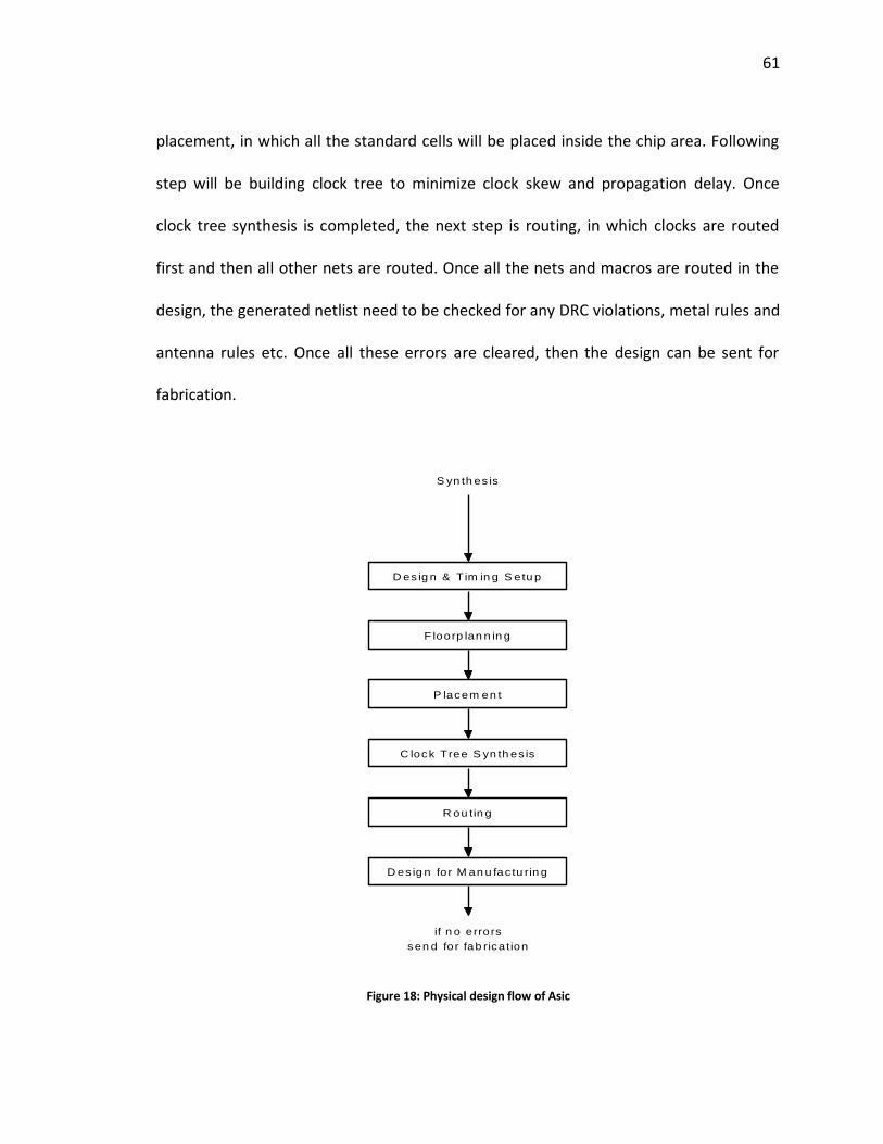
61
placement, in which all the standard cells will be placed inside the chip area. Following
step will be building clock tree to minimize clock skew and propagation delay. Once
clock tree synthesis is completed, the next step is routing, in which clocks are routed
first and then all other nets are routed. Once all the nets and macros are routed in the
design, the generated netlist need to be checked for any DRC violations, metal rules and
antenna rules etc. Once all these errors are cleared, then the design can be sent for
fabrication.
D es ig n & Tim in g S etu p
F loorp lan n in g
P lacem en t
C lock Tree S yn th es is
R ou tin g
D es ig n fo r M an u fac tu rin g
if n o errors
sen d fo r fab rica tion
S yn th es is
Figure 18: Physical design flow of Asic

62
6.2 Porting designs from FPGA to ASIC
Designs from FPGA can be ported to ASIC with minor or major modifications. Synopsys
design analyzer looks for certain format to be followed when the design need to be
synthesized. The major difference appears if there are any FPGA technology specific
blocks such as LUT based shift registers, BRAMs, embedded multipliers etc. These are
only embedded in FPGA, and the synopsys library will not have them. Changes need to
be done accordingly for a successful synthesis by synopsys design analyzer. In p-1 and
rho I am using BRAMs which are FPGA specific and these memories are replaced by
equivalent memory components from the memory database library.
6.3 Tools and Libraries
6.3.1 Tools
These are the list of the tools used for ASIC implementation.
Synthesis : Synopsys Design Analyzer
Physical Design: Astro
Static Timing Analysis: primetime
Formal Verification: Formality
6.3.2 Libraries
These are the libraries used for synthesis and implementation.
Standard Cell Libraries: cb13fs120_tsmc_max (tsmc 130 nm library)
Memory Libraries: ram32x64_max, ram32x32_max, ram32x128_max

63
Chapter 7: Results
7.1 FPGA Results
All the three architectures are developed entirely in RTL using VHDL. An effort is made
to make the codes as generic as possible so that the same code can be used across
different families of FPGAs and ASIC with minor modifications. The three architectures
i.e., rho, p-1 and unified rho and p-1 are implemented in three different families of
FPGAs i.e. Spartan 3, Spartan 3E and Virtex II. Initially all the single units are
implemented to calculate the resource utilization across three architectures and then
maximum number of units is implemented in all the three FPGA families to compare the
results. Apart from these three families of FPGAs, all the single units are implemented in
Virtex-4. Because of the limited system resources, maximum number of units couldn’t
be implemented in Virtex-4. For all FPGA implementations, all the codes were
synthesized using Synplify Pro 8.6 and implementation was done using Xilinx ISE 8.2i.
Functionality of all the units are thoroughly verified using test vectors provided by Paul
Kohlbrenner.

64
7.1.1 Memory Requirements
7.1.1.1 P-1
Memory requirements for the implementation of p-1 are shown in Table 3. For phase 1,
local memory has to hold the modulus, data from the pre-computations of sliding
window exponentiation and the final result. The amount of resources needed for pre-
computations depends on the size of the window. If the size of the window is w, the
number of pre-computed values is 2w-1-1. For the implementation of p-1, window size is
chosen as 5 and the number of pre-computations is 15. Apart from the pre-computed
values, the initial parameters needed for the implementation are g, g2 and 1 in
Montgomery domain. The intermediate and final result is also stored in local memory. If
we combine all these values, the local memory for phase 1 requires 19 registers. In
phase 2, size of the local memory depends on the number of gcd values. This number
depends on the parameter D. The gcd values computed in Phase 2 are stored in local
memory, as they are used for subtraction and accumulation. For D=210, there are 48
gcd values and each value requires 8 locations in the memory. Other than gcd values,
there are 4 other locations which are used for intermediate values during the
computation and the final result. After combining all these locations, local memory
requires 424 locations.

65
Table 3: Memory resources needed for p-1 hardware implementation
Objects # objects
#32-bit
words per objects
#
of words
#
of bits
Memory
size
#
BRAMs (512x32)
p-1 Local Memory- Phase 1
Registers 19 8 152 4864 256x32 1
p-1 Local Memory-Phase 1 & 2
Registers 53 8 424 13,568 512x32 1
Global Memory- Phase1 (14 units)
Registers 4*14 8 468 14,976
kN 1 1 1 32
k 1 43 43 1376
512 16,384 512x32 1
Global Memory- Phase 2
GCD_table 4 1 4 128
Mmin,MN 2 1 2 64
prime_table 402 402 402 12,864
408 13,056 512x32 1
Global memory size depends on the phase of the algorithm. In Phase 1, global memory
has the initial data needed for all individual units and the value of k, which is product of
primes and is common to all the units. Each unit needs the number to be factored n, the
initial values g,g2 and 1 in Montgomery domain. Size of the k, which is common to all
the units is 1375 bits, which occupy 43 locations and one location for the number of
words in k. The size of the global memory for Phase 2 is independent of the number of
units and depends on the parameters B1, B2 and D. For the values of B1 = 960, B2 =
57,000 and D = 210, the number of words in GCD_table are four and the number of
words in prime_table are 402. Including the values of Mmin and Mmax, the size of global

66
memory needed for Phase 2 is 408x32. For this requirement, the available size of BRAM
in FPGA is 512x32. When using 512x32 global memory for Phase 2, using the same size
for Phase 1 can hold the initial values needed for 14 units along with the value of k. The
size of the global memory for Phase 1 for m no. of units is m*32+44 words. Using the
same memory once all units are supplied with the parameters needed for Phase 1,
global memory can be loaded with the data needed for Phase 2.
7.1.1.2 Rho
Memory requirements for rho implementation are show in Table 4. As shown in Figure
13, local memory contains 6 registers and each register has 8 words. Thus the size of the
local memory is 64x32.
Table 4: Memory resources needed for rho implementation
Objects # objects #32-bit
words per
objects
#
words
#
bits
Memory
size
# BRAMs
(512x32)
Local Memory
Registers 6 8 48 1,536 64x32
Global Memory
Registers 5 8 40 1280
t 1 1 1 32
41 1312 64x32
67
Global memory will hold the parameters needed for each unit. The parameters n, x0, a,
d are different for different units and the number of iterations , which is common to all
the units. Based on these values and for the ease of implementation is loaded twice
in the local memory. As explained, global memory needs 41 locations for one unit. For m
number of units the size of the global memory is .
7.1.1.3 Unified rho and p-1
As explained in the architecture of unified unit, it has two local memories one for rho
and the other one for p-1. The contents and the size of these memories is the same as
explained in earlier sections.
Global memory for the unified unit has all the parameters needed for both rho and p-1.
If we combine the parameters and the values needed for both methods, global memory
requires 517 locations for a single unified unit. The size of the global memory with m
units is described as follow.
m*8 locations for the numbers to be factored
m*32 locations for parameters of rho
1 location for number of iterations in rho
m*24 locations for Phase 1 parameters of p-1
1 location for no. of words in k for p-1
43 locations for the value of k
408 values for the Phase 2 of p-1

68
Combining all these parameters and values results in the size of the global memory as
with unified units.
7.1.2 Timing Calculations for rho, p-1 and unified unit
The execution times for rho, p-1 and unified unit are explained in this section. Timing is
described in generic formulas for each method in the following sections. The timing
details of basic arithmetic blocks multiplier and adder/subtractor are shown in Table 5.
In this table n is the number of bits in the number to be factored. Number with 195 bits
is factored using Phase 1 and the corresponding clock cycles for multiplication and
addition are 41.
Table 5: Execution times of arithmetic blocks
Operation Notation Formula # clk cycles
Modular addition TA 41
Montgomery Multiplication
TM TM = n+16 211
7.1.2.1 Rho
The execution time of the rho method depends on the number of iterations t. From
Figure 9 and Algorithm 11, the total number of operations in the rho method with t
number of iterations is
2*t multiplications + 2*t additions

69
t-1 accumulations + t subtractions
As shown in Table 2, operations in the first rho and second rho are execute in parallel,
i.e., multiplier is loaded with the values and once the multiplication is started addition
or subtraction is finished in parallel. Thus addition or subtraction in all cases doesn’t
require extra time.
Total execution time for rho method ≈ (3t-1)TM + (t)TA
For t=1024 which is √220, the estimates and simulated timings are
Testrho = 689,965 clock cycles
Tsimrho = 703,125 clock cycles
This difference in the estimated and simulated timings is, timing information for control
operations and data movements is not included in the estimated timing.
7.1.2.2 P-1
The execution time of p-1 algorithm is shown in Table 6. This time consists of pre-
computation time and modular exponentiation time in Phase 1, gcd values computation
time and the accumulation time in Phase 2. The number of multiplications in Phase 1
depends on the value of k and the number of pre-computations.
Table 6: Timing calculations for Phase 1 and Phase 2 of p-1
Operation Notation Formula # clk cycles
Phase 1
Pre-computation TpreP1 Tpre = 15TM 3,165
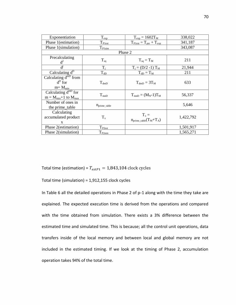
70
Exponentiation Texp Texp = 1602TM 338,022
Phase 1(estimation) TP1est TP1est = Tpre + Texp 341,187
Phase 1(simulation) TP1sim 343,087
Phase 2
Precalculating
d2
Tsq Tsq = TM 211
dj Tj Tj = (D/2 -1) TM 21,944
Calculating dD TdD TdD = TM 211
Calculating dmD
from
dD for
m= Mmin
TdmD TdmD = 3TM 633
Calculating dmD
for
m = Mmin+1 to Mmax TmnD TmnD = (MN-1)TM 56,337
Number of ones in
the prime_table nprime_table 5,646
Calculating
accumulated product
x
Tx Tx =
nprime_table(TM+TA) 1,422,792
Phase 2(estimation) TP2est 1,501,917
Phase 2(simulation) TP2sim 1,565,271
Total time (estimation) =
Total time (simulation) = 1,912,155 clock cycles
In Table 6 all the detailed operations in Phase 2 of p-1 along with the time they take are
explained. The expected execution time is derived from the operations and compared
with the time obtained from simulation. There exists a 3% difference between the
estimated time and simulated time. This is because; all the control unit operations, data
transfers inside of the local memory and between local and global memory are not
included in the estimated timing. If we look at the timing of Phase 2, accumulation
operation takes 94% of the total time.

71
7.1.2.3 Unified rho and p-1
Taking execution times of rho and p-1 into account, the execution time is addition of
execution times for unified unit. The estimated and simulated times for unified unit are
Tuniest (estimation) = clock cycles
Tunisim (simulation) = 2,614,746 clock cycles
As explained earlier, the difference between the estimated and simulated timings is the
timing for control operations and data movement inside the local memory and data
movement between local and global memories, which are not included in the estimated
time.
7.1.3 Area and Timing results from FPGA implementations
Table 7: FPGA implementation of single unit of rho
Results Virtex II
XC2v6000-6
Spartan 3
XC3S5000-5
Spartan 3E
XC3S1600E-5
Virtex 4
XC4VLX200-
11
Resources
-CLB Slices 1,680(4%) 1,740(5%) 1,778(12%) 1,785(2%)
-LUTs 2,714(4%) 2,845(4%) 2,905(9%) 2,903(1%)
-FFs 1,518(2%) 1,524(2%) 1,522(5%) 1,513(1%)
-BRAMs 0/144 0/104 0/36 0/336
Technology 0.15/0.12 um 90 nm 90 nm 90 nm
Max. Clock
Frequency
130 MHz 94 MHz 110 MHz 141 MHz
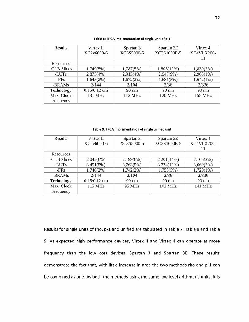
72
Table 8: FPGA implementation of single unit of p-1
Results Virtex II XC2v6000-6
Spartan 3 XC3S5000-5
Spartan 3E XC3S1600E-5
Virtex 4 XC4VLX200-
11
Resources
-CLB Slices 1,749(5%) 1,787(5%) 1,805(12%) 1,830(2%)
-LUTs 2,875(4%) 2,915(4%) 2,947(9%) 2,963(1%)
-FFs 1,645(2%) 1,672(2%) 1,681(5%) 1,642(1%)
-BRAMs 2/144 2/104 2/36 2/336
Technology 0.15/0.12 um 90 nm 90 nm 90 nm
Max. Clock
Frequency
131 MHz 112 MHz 120 MHz 155 MHz
Table 9: FPGA implementation of single unified unit
Results Virtex II
XC2v6000-6
Spartan 3
XC3S5000-5
Spartan 3E
XC3S1600E-5
Virtex 4
XC4VLX200-11
Resources
-CLB Slices 2,042(6%) 2,199(6%) 2,201(14%) 2,166(2%)
-LUTs 3,451(5%) 3,763(5%) 3,774(12%) 3,669(2%)
-FFs 1,740(2%) 1,742(2%) 1,755(5%) 1,729(1%)
-BRAMs 2/144 2/104 2/36 2/336
Technology 0.15/0.12 um 90 nm 90 nm 90 nm
Max. Clock
Frequency
115 MHz 95 MHz 101 MHz 141 MHz
Results for single units of rho, p-1 and unified are tabulated in Table 7, Table 8 and Table
9. As expected high performance devices, Virtex II and Virtex 4 can operate at more
frequency than the low cost devices, Spartan 3 and Spartan 3E. These results
demonstrate the fact that, with little increase in area the two methods rho and p-1 can
be combined as one. As both the methods using the same low level arithmetic units, it is
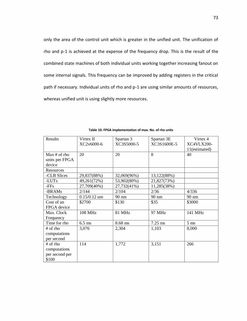
73
only the area of the control unit which is greater in the unified unit. The unification of
rho and p-1 is achieved at the expense of the frequency drop. This is the result of the
combined state machines of both individual units working together increasing fanout on
some internal signals. This frequency can be improved by adding registers in the critical
path if necessary. Individual units of rho and p-1 are using similar amounts of resources,
whereas unified unit is using slightly more resources.
Table 10: FPGA implementation of max. No. of rho units
Results Virtex II
XC2v6000-6
Spartan 3
XC3S5000-5
Spartan 3E
XC3S1600E-5
Virtex 4
XC4VLX200-
11(estimated)
Max # of rho units per FPGA
device
20 20 8 40
Resources
-CLB Slices 29,837(88%) 32,069(96%) 13,122(88%)
-LUTs 49,261(72%) 53,902(80%) 21,827(73%)
-FFs 27,709(40%) 27,732(41%) 11,285(38%)
-BRAMs 2/144 2/104 2/36 4/336
Technology 0.15/0.12 um 90 nm 90 nm 90 nm
Cost of an
FPGA device
$2700 $130 $35 $3000
Max. Clock
Frequency
108 MHz 81 MHz 97 MHz 141 MHz
Time for rho 6.5 ms 8.68 ms 7.25 ms 5 ms
# of rho
computations
per second
3,076 2,304 1,103 8,000
# of rho
computations
per second per
$100
114 1,772 3,151 266

74
Table 11: FPGA implementation of max. No. of p-1 units
Results Virtex II XC2v6000-6
Spartan 3 XC3S5000-5
Spartan 3E XC3S1600E-5
Virtex 4 XC4VLX200-
11(estimated)
Max # of p-1 units per FPGA
device
23 23 9 46
Resources
-CLB Slices 31,827(94%) 32,451(97%) 13,013(88%)
-LUTs 49,668(73%) 51,207(76%) 20,768(70%)
-FFs 31,942(47%) 31,949(48%) 12,754(43%)
-BRAMs 25/144 15/104 10/36 50/336
Technology 0.15/0.12 um 90 nm 90 nm 90 nm
Cost of an FPGA device
$2700 $130 $35 $3000
Max. Clock
Frequency
107 MHz 86 MHz 112 MHz 155 MHz
Time for p-1 17.88 ms 22.24 ms 17.08 ms 12.33 ms
# of p-1
computations
per second
1,286 1,034 527 3,730
# of p-1 computations
per second per
$100
47 795 1,505 124
FGPA implementations with maximum number of rho, p-1 and unified units are shown
in Table 10, Table 11 and Table 12. Resource utilization in terms of CLB slices, number of
BRAMs used, maximum clock frequency, execution time, computations per second and
computations when cost is taken into account are shown in the tables. As mentioned
before, due to limited number of system resources maximum number of units on Virtex
4 weren’t implemented. Instead these values are estimated considering the best case
for the comparison to be fair.

75
By looking at the results, low cost devices Spartan 3 and Spartan 3E outperform the high
performance Virtex II and Virtex4 devices in rho by factor of 15 and 12, in p-1 by factor
of 17 and 12 and by factor of 15 and 11 respectively and thus most suitable for code
breaking. Additionally the new generation devices Spartan 3E and Virtex 4 has better
performance than their previous generation devices Spartan 3 and Virtex II.
Table 12: FPGA implementation of maximum No of unified units
Results Virtex II
XC2v6000-6
Spartan 3
XC3S5000-5
Spartan 3E
XC3S1600E-5
Virtex 4
XC4VLX200-
11(estimated)
Max # of
unified units per
FPGA device
21 19 8 42
Resources
-CLB Slices 32,280(95%) 30,905(93%) 13,587(92%)
-LUTs 53,791(79%) 45,832(69%) 19,810(67%)
-FFs 29,268(43%) 27,894(41%) 11,392(38%)
-BRAMs 25/144 23/104 10/36 49/336
Technology 0.15/0.12 um 90 nm 90 nm 90 nm
Cost of an
FPGA device
$2700 $130 $35 $3000
Max. Clock
Frequency
102 MHz 80 MHz 95 MHz 141 MHz
Time for rho &
p-1
25.62 ms 32.68 ms 27.53 ms 18.56 ms
# of unified
computations per second
819 581 290 2,262
# of unified
computations per second per
$100
30 447 828 75

76
7.2 Area and Timing Results from ASIC implementations
All the three architectures are implemented in ASIC using 120 nm tsmc library and
shown in Table 13. The netlist generated after synthesis is verified for functional
equivalency against RTL using the tool called Formality. This process is known as Formal
Verification. In general the frequency of operation in ASIC is 2 to 2.5 times that of FPGA.
But I could never get more than 200 MHz in any of the cases. Initially I tried using 250
MHz as target frequency, and it resulted in lot of timing violations and DRC errors. Then
target frequency is decreased to 200 MHz, and there are no timing violations and DRC
errors. Even though some positive slack was obtained, I am using 200 MHz for the
comparison purposes. Maximum number of units couldn’t be implemented due to the
limited system resources available in the lab.
Table 13: Results from ASIC implementation
Operation rho p-1 Unified architecture
Area 1.15 mm2 1.21 mm
2 1.8 mm
2
Max. Clock
Frequency
200 MHz 200MHz 200 MHz
Time for execution 3.52 ms 9.56 ms 13.1 ms
# of operations per
second (using
maximum no. of units)
96,022 34,100 16,615
Core utilization ratio 70% 70% 65%

77
When 20 rho units are implemented in ASIC the results are shown in Figure 19. The
improvement in terms of area is about 51. The area factor of 50 is reasonable [19] for
this kind of circuit, where logic and memory are being used. This factor may be less for
p-1 and unified architecture, as they need more area for memory.
Figure19: ASIC layout of 20 units of rho

78
7.3 Comparison of FPGA and ASIC Results
Before comparing the performance of FPGA and ASIC, we need to determine how many
units will fit on ASIC with the same area as Virtex II, as Virtex II is the closest match with
the ASIC technology used for implementations. Area of Virtex II FPGA is 19.68 x 19.8
mm2 (estimation by R.J. Lim Fong, MS Thesis, VPI, 2004).
When the same area is considered for ASIC implementation, ASIC can fit 338 units of
rho, 322 units of p-1 and 216 units of unified rho and p-1. The number of computations
will be much more than in FPGA. This is because the effective utilization of area and high
frequency of operation in ASIC. The maximum number of units can be implemented on
the ASIC is more than the estimation. The factors which affect the maximum number
are as follows: With the present comparison in ASIC there is one control unit for one
execution unit, which is not true for FPGA and will not be that way when actually
implemented on ASIC. Another factor is size of the global memory. Now for one unit size
of the global memory is 512x32 and it is not linearly related to the no. of units. Global
memory occupies large portion of the area and if properly managed, more number of
units can be implemented on the chip. But for comparison purposes, all the calculations
are done using the numbers presented in this section. If we compare the number of
operations per second ASIC dominates FPGA with a factor of 31 for rho, with a factor of
27 for p-1 and with a factor of 21 for the unified unit. If all the above mentioned factors
are considered, these factors may go up to 65-80.

79
Chapter 8: Summary and Conclusion
A novel architecture for rho, p-1 and unified architecture has been proposed. P-1 and
rho methods are implemented in hardware for the first time. The three architectures
i.e., rho, p-1 and unified rho and p-1 are implemented in two different technologies
FPGA and ASIC. In FPGA, all these architectures are implemented in four different
families of FPGA. From the FPGA implementation results, it shows that low cost devices
such as Spartan 3 and Spartan 3E outperform the high performance devices Virtex II and
Virtex 4 by factor of 15 and 11 in the case of unified architecture when number of
operations per unit of time and cost is considered. It is also shown that with little
overhead in area both methods i.e., rho and p-1 can be integrated into one unit. This
unification may find more than one factor and has more probability of finding a factor,
as it executes both algorithms sequentially. When implemented in ASIC, the hardware
resources are effectively used and it is possible to fit significantly more units than in
FPGA. Area of Virtex II is considered for comparison purposes as its technology is the
closet possible technology of the ASIC used. In terms of frequency ASIC achieved
approximately 1.5 times the frequency of FPGA. An ASIC chip, which has similar area of
a Virtex II FPGA can fit 332 units of rho, 322 units of p-1 and 216 unified units. The
number of computations performed by ASIC is better than FPGA by a factor of 31 for
80
rho, 27 for p-1 and 26 for unified architecture. These numbers are calculated when the
resources on ASIC are least efficiently used. If all the resources on ASIC are utilized
properly these numbers increase, at least by a factor of 3-5. When produced in a larger
number (greater than 100,000) to overcome the non-recurring cost ($1,000,000), ASIC is
better technology as it effectively uses the area and gives better frequency. When the
mass production is not considered as an option, suitable devices for code-breaking are
low cost devices such as Spartan 3 and Spartan 3E.
The unified unit of rho and p-1 is using slightly more resources than individual units, but
it has more probability of finding the factors. If this unified unit is combined with the
ECM [5] and trial division, it is capable of implementing the whole post-sieving phase of
NFS. This combined unit will have more chances of finding factor(s). ECM was
implemented using two multipliers and one adder/subtractor, whereas unified
architecture has only one multiplier and one adder/subtractor. Implementing trial
division in hardware, re-designing ECM with one multiplier and one adder/subtractor
and combining all the methods is a possible direction for future work.

81
BIBLIOGRAPHY
82
BIBLIOGRAPHY
[1] C. McIvor, M. McLoone, J. McCanny, A. Daly and W. Marnane, Fast
montgomery modular multiplication and rsa cryptographic processor
architectures,"Proc. 37th IEEE Computer Society Asilomar Conference on
Signals, Systems and Computers, pp. 379-384, Nov 2003.
[2] K Gaj, S Kwon, P Baier, P Kohlbrenner, H Le, M Khaleeluddin and R
Bachimanchi, Implementing the elliptic curve method of factoring in
reconfigurable hardware." in Proc. Cryptographic Hardware and Embedded
Systems Workshop, CHESS 2006, Yokohama, Japan, Oct 2006.
[3] A. Menzes, P. van Oorschot, and S. Vanstone, Handbook of Applied
Cryptography, CRC Press, 1996.
[4] Per Leslie Jensen, Master’s Thesis on Integer Factorization, Department of
Computer Science, University of Copenhagen, Fall 2005.
[5] Mohamed Khaleeluddin, Master’s Thesis on Hardware Implementation of The
Elliptic Curve Method of Factoring, Department of Electrical and Computer
Engineering, George Mason University, Summer 2006.
[6] J. M. Pollard, Factoring with cubic integers," in Lecture Notes in Mathematics
1554. Springer-Verlag, 1993, pp. 4-10.
[7] F. Bahr, M. Boehm, J. Franke and T. Kleinjung, Factorization of rsa-200."
[Online]. Available: http:crypto-world.com/announcements/rsa200.txt
[8] R. P. Brent, Some integer factorization algorithms using elliptic curves,"
Australian Computer Science Communications, vol. 8, pp. 149-163, 1986.

83
[9] H. W. Lenstra, Factoring integers with elliptic curves," Annals of Mathematics,
vol. 126, no. 2, pp. 649-673, 1987.
[10] P. L. Montgomery, Modular multiplication without trivial division,"
Mathematics of Computation, vol. 44, pp. 519-521, 1985.
[11] P. L. Montgomery, Speeding the pollards and elliptic curve methods of
factorization," Mathematics of Computation, vol. 48, pp. 243-264, 1987.
[12] P. L. Montgomery, An FFT extension of the elliptic curve method of
factorization," Ph.D. dissertation, UCLA, 1992.
[13] J. M. Pollard, A monte carlo method for factorization," Nordisk Tidskrift for
Informationsbehandlung (BIT), vol. 15, pp. 331-334, 1975.
[14] John M. Pollard, Theorems on factorization and primality testing., Proceedings
of the Cambridge Philosophical Society 76 (1974), 521–528.
[15] Richard P. Brent, An improved Monte Carlo factorization algorithm, BIT 20
(1980), 176–184.
[16] W. Stallings, Cryptography and Network Security, 3rd ed. Prentice Hall, 2003
[17] Ian Kuon and Jonathan Rose, Measuring the Gap Between FPGAs ad ASICs,
IEEE Transactions on Computer-Aided Design of Integrated Circuits and
Systems, vol. 62, no. 2, Feb 2007.

84
Curriculum Vitae
Ramakrishna Bachimanchi received his Bachleor of Engineering Degree from Osmania University, Hyderabad, India in 2004. He has been involved with teaching various undergraduate and graduate courses at George Mason University, both as a teaching assistant and a lab instructor.