fox ii 286 - minus zero degrees - fox-ii 286 (12...fox-ii is available in two versions, 12mhz and...
TRANSCRIPT

) )
FOX II 286
) )
, I ,-, ~,
on
) )
/ '-
"t,.
'-,1 f ..,.t:
RADIO FREQUENCY INTERFERENCE STATEMENT
This equipment generates and uses radio frequency energy and if not installed and used properly, that is, in strict accordance with the manufacturer's instructions, may cause 'interference with radio and television reception,
If this equipment does cause interference to radio or TV reception, which can be determined by turning the equipment off and on, the user is encouraged to try to correct the interference by one or more of the following measures:
* * * *
*
*
*
Reorient the receiving antenna. Relocate the computer away from the receiver. Move the computer away from the receiver. Plug the power cord of computer into a different outlet so that computer and receiver are on different branch circuits. Ensure tha t card slot covers are in place when no card is installed. Ensure that card mounting screws, attachment connector screws, and ground wires are tightly secured. If peripherals are used with this system, it is suggested to use shielded, grounded cables, with in-line filters if necessary.
If necessary, the user should consult the dealer service representative for additional suggestions.
The manufacturer is not responsible or TV interferences caused by modifications to this equipment. responsibility of the user to interferences.
for any radio unauthorized
It is the correct such
OPERATION AND MAINTENANCE
l'
THIS PAGE IS INTENTIONALLY LEFT BLANK
B-4
Preface
This manual covers the necessary information to operate the FOX-II system board. In-depth explanations of the functions of the motherboard are provided. The table of contents gives detailed information about the arrangement of this manual. The system BIOS setup is further discussed in the appendix.
The content in this manual is only for reference and is intended to provide basic informa tion for the general users. There are also technical information provided for hardware and software engineers.
The man ual compose of 4 chapters, chapter contains a brief introduction of FOX-II
motherboard. In the chapter 2, specifica tions and functions of FOX-II are discussed. It also outlines many advanced features of the CPU and the system architecture. Chapter 3 deals with the installa tion of coprocessor, DRAM modules, jumpers and the memory configurations. Technical information is provided in the chapter 4.
System BIOS and the system further described in the appendix A. procedures are explained.
Note:
setup are All setup
FOX-II is available in two versions, 12MHz and 16MHz; which are further classified into 2 categories - with or without memory modules. Features and functions described in the manual is identical for each version except for their operating frequencies and memory configurations.

OPERATION AND MAINTENANCE
KEEPING THE SYSTEM COOL
Airflow is critical for proper operation. The motherboard contains many high-speed componen ts and they will generate heat during opera tion. Other add-on cards and hard disk drive can also produce a lot of heat. As a result , the temperature inside the computer system may be very high. These boards require cool air to prevent a deadly heat build-up. Be sure that all cooling vents in the front or sides of the computer are open and that air circulation is good. Check the clearance at the back of the computer; the power supply contains a fan to blow air out of the case, make sure the fan is not blocked by ca bles or papers. Don't push your computer flush against the wall; leave it some breathing space. Heat can destroy computer chips.
CLEANING THE "GOLDEN FINGER"
Whenever inserting an add-on card to the motherboard, make sure that there is no dirt on the "golden finger" of the add-on card. If not, the contact between the "golden finger" and the slot may be poor and thus causing the add-on cards to work improperly. Use a pencil eraser to clean the "golden finger" if dirt is found.
B-2
CONTENT
Chapter I INTRODUCTION
Chapter 2 GENERAL FEATURES
Specification Processor Math Coprocessor Memory System I/O Subsystem System Functions
1-1
2-1
2-1 2-3 2-6 2-8 2-10 2-10
Chapter 3 INSTALLING COMPONENTS 3-1
Installing 80287 Math Coprocessor System Memory Configuration Control of System Speed System Board Jumper Setting System Board Connectors
3-1 3-4 3-9 3-10
3-11
SYSTEM BIOS
THIS PAGE IS INTENTIONALLY LEFT BLANK
A-20
CHAPTER 1 INTRODUCTION
The FOX-II system board is a cost-effective, mid-range performance system board that is designed for PC/AT compatible application. It offers an increased power and flexibility architecture by supporting 80286 processor speeds up to 16 MHz. (See NOTE on PREFACE)
For the memory system, it is configurable from 256K to 4 MByte of DRAMs on the system board with true "0" wait state DRAM accesses. Hardware EMS is implemented with 4 registers. In addition to it, System and Video shadowing features are also supported in 16K blocks. It is also optimized to allow mixing of DRAM types to give end user the maximum flexibility in choosing the correct DRAM capacity for their applications. This flexibility in configuration allows you to select an ideal cost/performance combina tion.
FOX-II is a fully PC/ A T compa tible system board implemented with a highly integrated chip sets to provide high performance, reliability and compa ti bili ty. This means tha t virtually all the hardware and software that is available for the PC/ A T can also be run on a system you build around the FOX-II system. It supports MS-DOS, Xenix, Unix and all PC/AT application programs. Users can run applications designed for the PC/ AT on FOX-II without any modification. Multi-tasking and multi-user capabilities are fully functional on this system board.
1-1
SYSTEM BIOS
RUNNING AMI BIOS DIAGNOSTICS
Follow initial procedures in the CMOS Setup until the following display is shown on the screen:
EXIT FOR BOOT RUN CMOS SETUP RUN DIAGNOSTICS
Use the <Up> & <Down> to move the highlight bar to select "RUN DIAGNOSTICS" and then press <Enter>. A diagnostic menu will soon appear on the screen.
The AMI Diagnostics provides an easy to operate screen-menu allowing inexperienced users to operate the program. Simply press <Left> or <Right> and <Up> or <Down> keys to move the highlight bar the option desired.
The diagnostics program performs specialized tests on each of the following when instructed.
A-lS
Hard disk drive(s) - Floppy disk drive(s) - Keyboard
Video adapter board and monitor - Printer and Communication ports
CHAPTER 2 GENERAL FEATURES
SPECIFICATION
Processor Subsystem
80286 CPU Optional 80287 co-processor
Speed:
Turbo/normal speed Software/hardware selectable
Memory Subsystem:
4MB using I M SIMMs 1MB using 256Kbx4 DRAM chips or 256K SIMMs Support memory mixing of 256K and 1M System BIOS shadow Video BIOS shadow Hardware EMS implementation 128K or 256K Eprom BIOS o or 1 wait state selectable
2-1
SYSTEM BIOS
OPTION 11 MEMORY RELOCATION
If your system memory is 1 MByte, ena ble this feature. In that case you can remap the 384KB memory so that the memory which is neither used as EMS nor shadow RAM can be used as ex tended memory. Note that this option is applicable only for the 1 MByte memory configura tion.
a) Enabled * b) Disabled
* BIOS Default
A-16
GENERAL FEATURES
PROCESSOR
The 80286 is an advanced, high-performance microprocessor with specially optimized capabilities for multiple user and multi-tasking systems. The 80286 has built-in memory protection that supports opera ting system and task isola tion as w'ell as program and da ta pri vacy within tasks. The 80286 includes memory management capabilities that map 230 (one gigabyte) of virtual address space per task into 224 bytes (16 megabytes) of physical memory.
The 80286 is upward compatible with 8086 and 8088 software. Using 8086 real address mode, the 80286 is object code compatible with existing 8086,88 software. In protected virtual address mode, the 80286 is source code compatible with 8086, 88 software and may require upgrading to use virtual addresses supported by the 80286's integrated memory management and protection mechanism. Both modes operate at full 80286 performance and execute a superset of the 8086 and 88 instructions.
The 80286 provides special operations to support the efficient implementation and execution of operating systems. For example, one instruction can end execution of one task, save its state, switch to a new task, load segment-notpresent exception and restartable instructions.
The 80286 operates in two modes: protected virtual address and real address.
2-3
SYSTEM BIOS
OPTION 7 SCRATCH RAM
The BIOS may require memory storage for certain functions and the storage can be allocated in two ways. One way is to use the BIOS stack and another is to allocate a IK bytes memory in the base memory. Generally, the former option is appropriate. If the hard disk type 47 is defined or if you run program like OS/2, select the option 2.
OPTION 8 MAIN BIOS SHADOW
Main BIOS Shadow can be selected in this men u. If you ha ve system memory of I MB or more, enable Main BIOS shadow for a more efficient system. The Main BIOS will be shadow at FOOOOh. You cannot ena ble this option if your system memory is less than 1MB.
a) Disabled * b) Enabled
GENERAL FEATURES
Real Address Mode
In this mode, physical memory is a contiguous array of up to I megabyte. The selector portion of the pointer is interpreted as the upper 16 bits of a 20-bit address, and the remaining 4 bits are set to zero. This mode of operation is compatible with the 8088 and 8086.
Segments in this mode are 64KB in size and may be read, written or executed. An interrupt may occur if data operands or instructions attempt to wrap around the end of a segment. In this mode, the information contained in the segment does not use the full 64KB, and the unused end of the segment may be overlay by another segment to reduce physical memory requirements.
SYSTEM BIOS
When you install a new hard disk, make sure whether it is already formatted. If not, the BIOS has to check for a while before reporting the hard disk error. In fact, the error arises only because the hard disk is not formatted. If the hard disk is formatted, you can run DOS FDISK and DOS FORMAT.
Some fixed disks are specially handled and must be set to 'Not Installed'. Consult the fixed disk manual for details.
OPTION 4 DISPLAY
Four types of display are supported:
1. CGA 80 column mode 2. CGA 40 column mode 3. EGA and VGA 4. Monochrome
If the type of display is incorrect, the BIOS will prompt you and ask you to set up again. But the BIOS is still able to display messages on the display attached to the system. Thus you can en ter the setup program.
The jumper JP4 must be set according to this setting. Otherwise, the BIOS will report error after self-test.
A-12
GENERAL FEATURES
OP codes and operands through these I/O ports. The microprocessor also receives and stores results through the same I/O ports. The "BUSY" signal generated by the coprocessor signifies to the microprocessor to wait until the coprocessor has finished executing.
The following describe the mathematics coprocessor con trol ports:
OFO The latched Mathematics Coprocessor busy signal can be cleared with an 8- bit, Out command, to port FO. The coprocessor will latch "BUSY", if it asserts its error signal. Data output should be zero.
OF 1 The Mathematics Coprocessor will reset to real address mode which is in the 8087 compatible if an 8- bit Out command is sent to port FI. Again, the data output should be zero.
2-7
SYSTEM BIOS
CMOS SETUP OPTIONS
Following is a detail explanation of each CMOS Setup option.
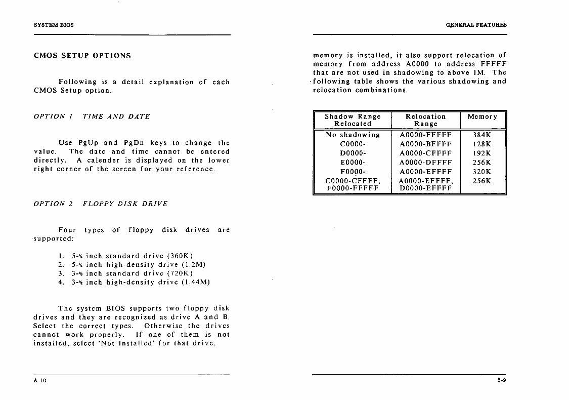
OPTION 1 TIME AND DATE
Use PgUp and PgDn keys to change the value. The date and time cannot be entered directly. A calender is displayed on the lower right corner of the screen for your reference.
OPTION 2 FLOPPY DISK DRIVE
Four types of floppy disk drives are supported:
l. 5-'14 inch standard drive (360K) 2. 5-'14 inch high-density drive (l.2M) 3. 3-'1. inch standard drive (720K) 4. 3-'1. inch high-density drive (l.44M)
The system BIOS supports two floppy disk drives and they are recognized as drive A and B. Select the correct types. Otherwise the dri ves cannot work properly. If one of them is not installed, select 'Not Installed' for that drive.
A-IO
G~NERAL FEATURES
memory is installed, it also support relocation of memory from address AOOOO to address FFFFF that are not used in shadowing to above 1M. The
. following table shows the various shadowing and reloca tion combinations.
Shadow Range Relocation Memory Relocated Range
No shadowing AOOOO-FFFFF 384K COOOO- AOOOO-BFFFF 128K DOOOO- AOOOO-CFFFF 192K EOOOO- AOOOO-DFFFF 256K F0090- AOOOO-EFFFF 320K
COOOO-CFFFF, AOOOO-EFFFF, 256K FOOOO-FFFFF DOOOO-EFFFF
2-9
SYSTEM BIOS
Once you have entered the SETUP menu, enter the date, time, the primary display type, the floppy drive installed and the hard disk drive type (if installed). The SETUP program will automatically determines your computer's memory configuration and displays it on the SETUP menu.
A-8
CHAPTER 3 INST ALLING COMPONENTS
Warning: Be sure to turn off the computer's power switch before installing or replacing any component.
If installation sounds risky, let your dealer install the 80287. If you make a mistake, you could damage the 80287 or your computer.
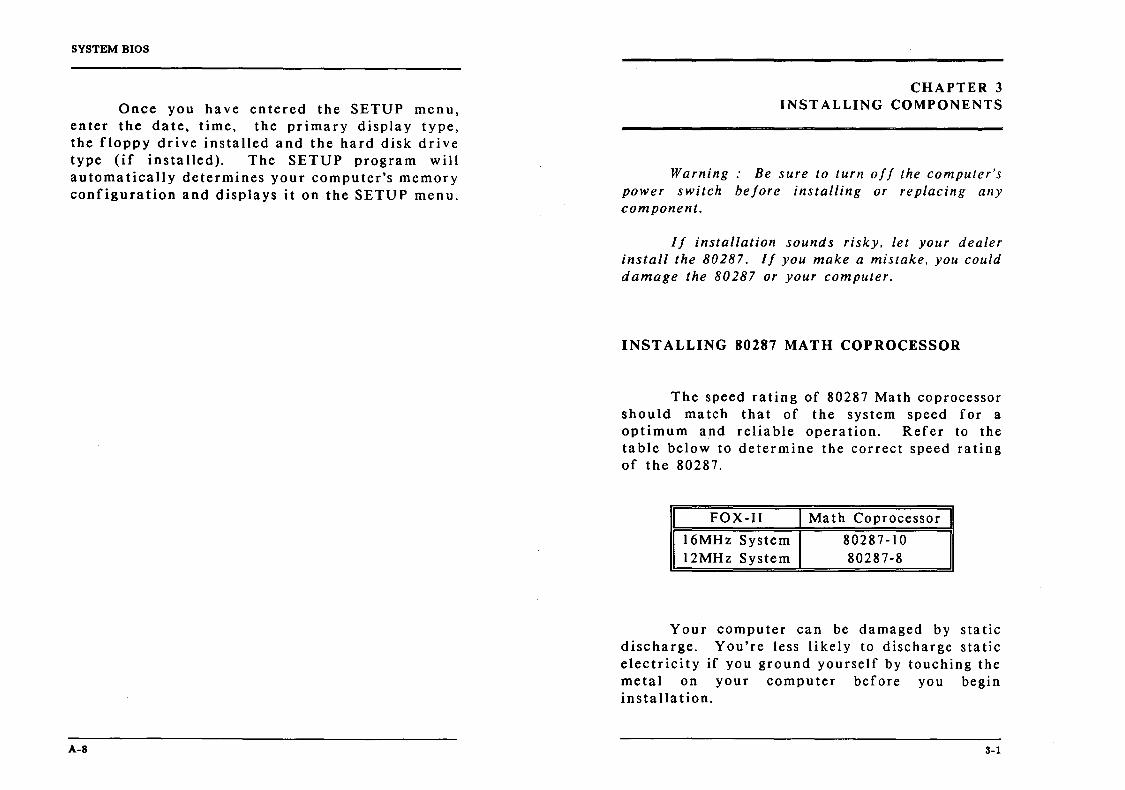
INST ALLING 80287 MATH COPROCESSOR
The speed rating of 80287 Math coprocessor should match that of the system speed for a optimum and reliable operation. Refer to the table below to determine the correct speed rating of the 80287.
I FOX-II I Math Coprocessor I 16MHz System 80287-10 12MHz System 80287-8
Your computer can be damaged by static discharge. You're less likely to discharge static electricity if you ground yourself by touching the metal on your computer before you begin installation.
3-1

SYSTEM BIOS
CMOS SETUP
Note: The BIOS may be updated from time to time. the one you got may not be exactly as discussed; this section will also be updated as necessary.
Follow the instructions as they come up on the screen to complete the ini tial proced ure. The ini tial prompt on the screen tells you to press the <DEL> key if you want to use the setup program. It is displayed briefly just after the RAM test is run when you first turn on the system. If it disappears before you have a chance to respond turn the system off and on again or reset the system and the message will reappear. The initial screen prompt will be similar to :
Press <DEL> key if you want to run SETUP or DIAGS.
Hi t <DEL> key to get in to the Setup Mode. (Note that <DEL> key will get you into the setup mode, only when the above message is displa yed on the screen.)
Upon your pressing of the <DEL> key, the following message will appear on the screen:
A-6
EXIT FOR BOOT RUN CMOS SETUP RUN DIAGNOSTICS
INSTALLING COMPONENTS
Illustration are given below.
80287
Notch
~ 00000000000000000000
D
00000000000000000000
80287 SOCKET
Check whether the system BIOS can detect the coprocessor upon power up. The system BIOS will display a list of devices on the motherboard after self-test. If the coprocessor is installed, it should show the type of coprocessor.
3-3

SYSTEM BIOS
The other type of errors are serious fail ure and are conveyed as a number of beep and repeated infinitely.
Beep Count Meaning I DRAM Refresh Failure 3 Base 64K Byte Memory Failure 4 System Timer Failure 5 Processor Failure 6 Keyboard Controller - Gate A20
Failure 7 Virtual Mode Exception Error 9 ROM-BIOS Checksum Failure
If no error is found during self-test, the system BIOS will proceed to boot from floppy disk or hard disk. The system BIOS will list the system configuration on the screen similar to below.
System Configuration (C) Copyright 1985-1990, American Megatrends Inc.,
Main Processor : 80286 Base Memory Size : 640 KB
Numeric Processor : None Ext. Memory Size : o KB
Floppy Drive A: : 1.2 MB, 5'1." Hard Disk C: Type : 2
Floppy Drive B: : 1.44MB, 3'1," Hard Disk D: Type : None
Display Type : VGA or EGA Serial Port(s) : None
ROM-BIOS Date : 6/13/90 Parallel Port(s) : 3BC
A-4
INSTALLING COMPONENTS
Dip Memory Configuration
I Memory Bank I Memory Location I DRAM Size I
*
BANK ° U22, U23, U27, U28 44256 U18, UI9 (parity) 41256
BANK I U24, U25, U29, U30 44256/4464* U20, U21 (parity) 41256/4164*
For the special case of 640K memory configuration, use the combination of 4464/4164 DRAM size in 'BANK l' for a more cost / effective solution.
'UI8,UI9' & 'U20,U21' are the parity bits for BANK 0 and BANK I respectively. These sockets can be left blank if parity checking logic is not desirable.
There are several combinations of DRAM types you may consider. So, a basic system can be equipped with fewer memory and later more memory can be installed when upgrading the system. As a typical case, a basic system can be equipped with 512 Kbyte memory using 256K DIP DRAM and then memory size is la ter increased to 2.5 Mega bytes by putting another 2 banks of 1 M SIMM. The memory size is detected automatically by system BIOS and indicated during memory test after power up. No switches or jumpers are required to be set for the memory size and DRAM type.
3-5
SYSTEM BIOS
If it is the first time that the computer is started up, you will need to configure the system by telling the SETUP program what hardware configura tion your system con tains.
The SETUP is a program that resides in the BIOS and is called up every time the system boots up. It lets you specify your system's configuration of diskette drives, hard disk drives, video display, memory, date and time. The AMI BIOS SETUP provides a one-screen interactive equipment and machine configuration setup. It can be run after the system has been turned on and the memory test is finished or has been escaped. The SETUP program is built-in, you do not need a diskette to use it.
If your FOX-II is already installed in a working system, you will not need to use the SETUP program unless the configuration already recorded in the on-board CMOS RAM is lost or a change is made in your system hard ware configuration. If the information is lost due to loss of battery power, you will need to reenter the configura tion.
A-2
INSTALLING COMPONENTS
Installing SIMM Modules
Whenever adding memory modules to the motherboard, install 2 modules at a time. Also make sure that the SIMM is installed in the correct orientation, the chips on the modules should be facing the I/O expansion slots. See the following page for the correct orientation of the memory modules.
To install a module, the module edge should angled into the socket's contact and then the module is pivoted into position, where the locking latches will secure it. If the module edge is not completely inserted into the socket, it cannot be pivoted to be in vertical position and should be dragged out and inserted again. Do not force the module into the SIMM socket. It will damage the locking latches.
The modules should be locked by the locking latches of the sockets firmly. Please check carefully before turning on the power. Otherwise, the system will not work properly.
3-7

TECHNICAL INFORMATION
I/O Channel (D-Side)
I I/O Pin Signal Name Dl -MEM CS16 D2 -I/O CS16 D3 IRQIO 04 IRQll D5 IRQ12 D6 IRQ15 D7 IRQ14 D8 -DACKO D9 ORQO
010 -DACK5 Dll DRQ5 D12 -OACK6 D13 DRQ6 014 -DACK7 015 DRQ7 D16 +5 Vdc D17 -MASTER D18 GND
4-18
I/O I I I I I I I 0 I 0 I 0 I 0 I
Power I
Ground
INSTALLING COMPONENTS
CONTROL OF SYSTEM SPEED
System Speed can be selected by hard ware switch and keyboard. Connector P3 should be connected to the turbo switch of the case panel. This controls the operation mode between turbo and normal mode, it will toggle between the 2 modes when pressed.
In addition to the front-panel switch, you can also change the system speed via keyboard. Press 'etrI', 'Alt' and '+' for turbo mode and 'Ctrl', 'Alt' and '-' for normal mode.
In either case, the turbo LED will light up to indicate whether the system is now running in turbo mode or normal mode. In turbo mode, the turbo LEO will turned on. In normal mode, the turbo LEO is off.
It should be note that turbo switch setting will override the keyboard switching mode, but not vice versa.
3-9
TECHNICAL INFORMATION
I/O Channel (B-Side)
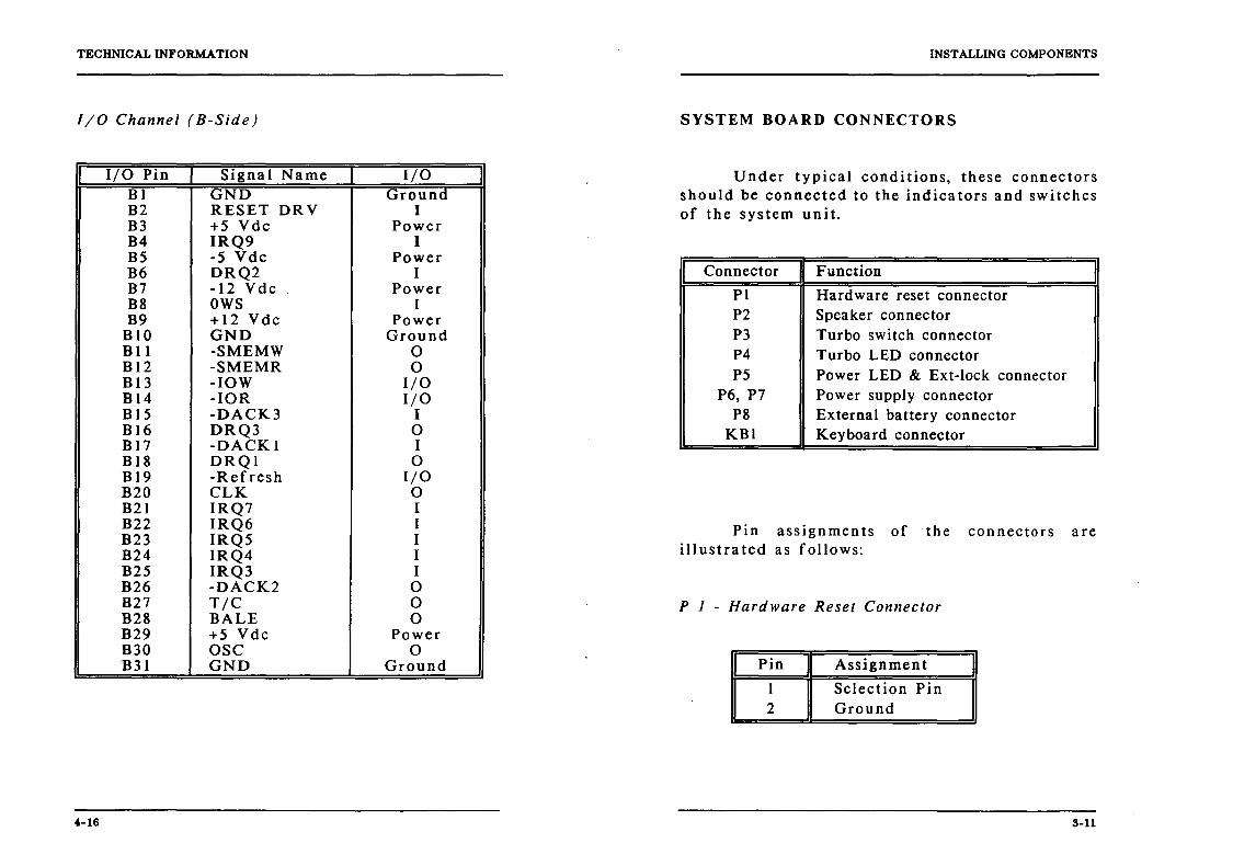
I I/O Pin I Signal Name I Bl GND B2 RESET DRV B3 +5 Vdc B4 IRQ9 B5 -5 Vdc B6 DRQ2 B7 -12 Vdc B8 OWS B9 +12 Vdc
BIO GND B II -SMEMW BI2 -SMEMR BI3 -lOW BI4 -lOR BI5 -DACK3 BI6 DRQ3 BI7 -DACKI Bl8 DRQI Bl9 -Refresh B20 CLK B21 IRQ7 B22 IRQ6 B23 IRQ5 B24 IRQ4 B25 IRQ3 B26 -DACK2 B27 T/C B28 BALE B29 +5 Vdc B30 OSC B31 GND
4-16
I/O I Ground
I Power
I Power
I Power
I Power
Ground 0 0
I/O I/O
I 0 I 0
I/O 0 I I I I I 0 0 0
Power 0
Ground
INSTALLING COMPONENTS
SYSTEM BOARD CONNECTORS
Under typical conditions, these connectors should be connected to the indicators and switches of the system unit.
Connector Function
PI Hardware reset connector P2 Speaker connector P3 Turbo switch connector P4 Turbo LED connector P5 Power LED & Ext-lock connector
P6, P7 Power supply connector P8 External battery connector
KBI Keyboard connector
Pin assignments of the connectors are illustrated as follows:
P J - Hardware Reset Connector
Pin Assignment
1 Selection Pin 2 Ground
3-11

TECHNICAL INFORMATION
The following figure shows the pin numbering for I/O channel connectors JB1,JB3,JB4 & JB6.
REAR PANEL
01 C1
010 C10
018 C18
COMPONENT SIDE
4-14
INSTALLING COMPONENTS
P 5 - Power LED & Ext-Lock Connector
Pin Assignment
1 +5 Vdc 2 Key 3 Ground 4 Keyboard inhibit 5 Ground
P6,P7 - Power Supply Connector
Pin Assignment
1 POWERGOOD 2 +5 Vdc 3 +12 Vdc 4 -12 Vdc 5 Ground 6 Ground
I Pin I Assignment
1 Ground 2 Ground 3 -5 Vdc 4 +5 Vdc 5 +5 Vdc 6 +5 Vdc
3-13
TECHNICAL INFORMATION
SYSTEM EXPANSION BUS
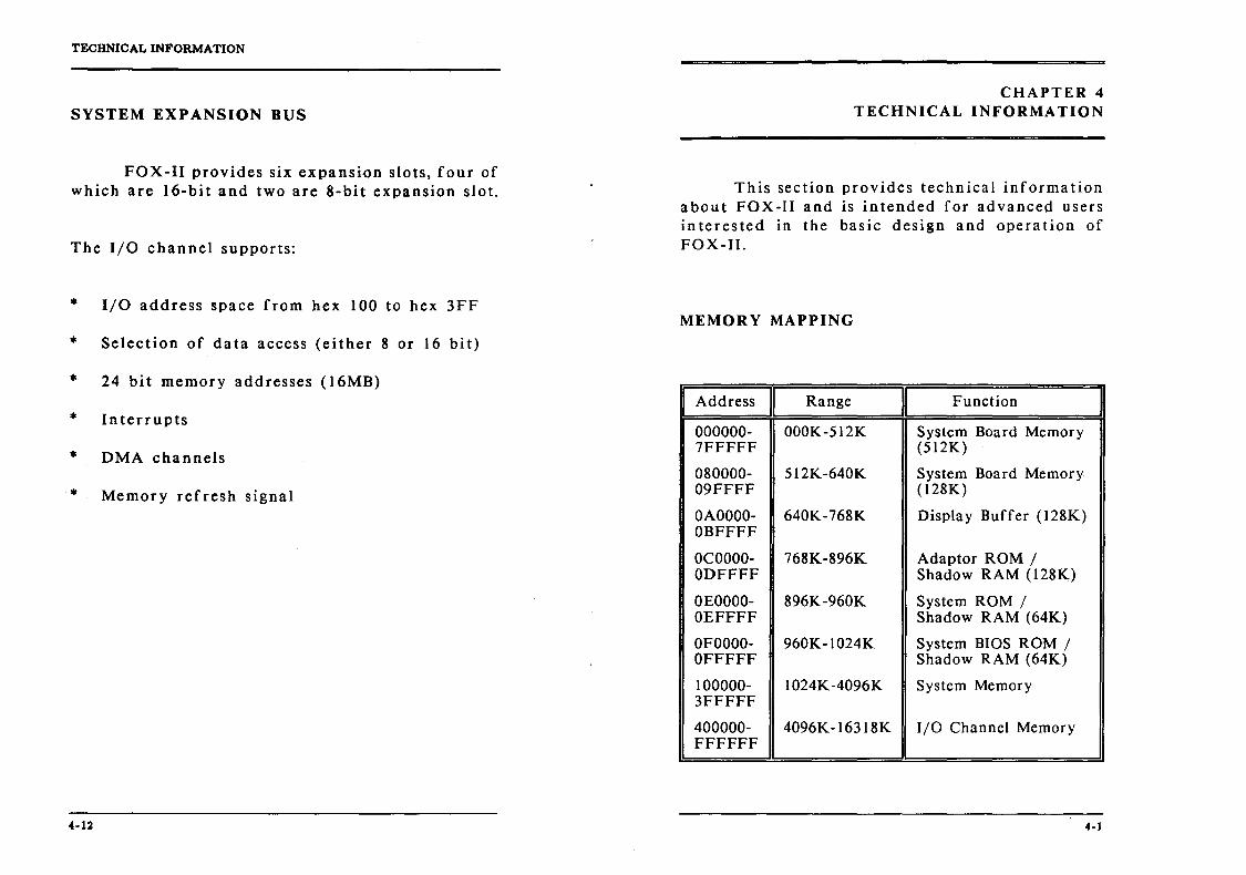
FOX-II provides six expansion slots, four of which are 16-bit and two are 8-bit expansion slot.
The I/O channel supports:
• I/O address space from hex 100 to hex 3FF
• Selection of data access (either 8 or 16 bit)
• 24 bit memory addresses (16MB)
• Interrupts
• DMA channels
• Memory refresh signal
4-12
CHAPTER 4 TECHNICAL INFORMATION
This section provides technical information about FOX-II and is intended for advanced users in teres ted in the basic design and operation of FOX-II.
MEMORY MAPPING
Address I Range II
Function I 000000- 000K-S12K System Board Memory 7FFFFF (SI2K)
080000- S12K-640K System Board Memory 09FFFF (128K)
OAOOOO- 640K-768K Display Buffer (128K) OBFFFF
OCOOOO- 768K-896K Adaptor ROM / ODFFFF Shadow RAM (l28K)
OEOOOO- 896K-960K System ROM / OEFFFF Shadow RAM (64K)
OFOOOO- 960K-I024K System BIOS ROM / OFFFFF Shadow RAM (64K)
100000- 1024K-4096K System Memory 3FFFFF
400000- 4096K-16318K I/O Channel Memory FFFFFF
4-1
TECHNICAL INFORMATION
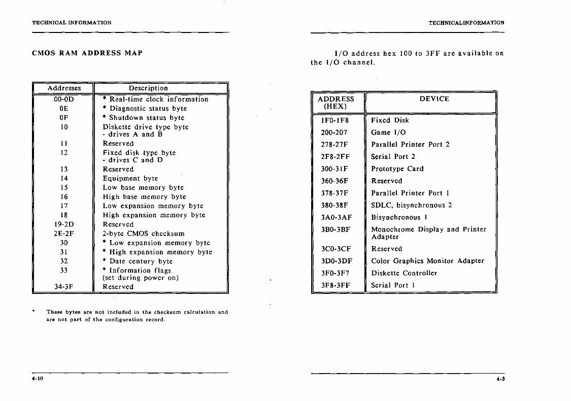
CMOS RAM ADDRESS MAP
I
•
4-10
Addresses I Description
OO-OD • Real-time clock information OE • Diagnostic status byte OF • Shutdown status byte 10 Diskette drive type byte
- drives A and B 11 Reserved 12 Fixed disk type byte
- drives C and D 13 Reserved 14 Equipment byte 15 Low base memory byte 16 High base memory byte 17 Low expansion memory byte 18 High expansion memory byte
19-2D Reserved 2E-2F 2-byte CMOS checksum
30 • Low expansion memory byte 31 • High expansion memory byte 32 • Date century byte 33 • Information flags
(set during power on) 34-3F Reserved
These bytes are not included in the checksum calculation and are not part of the configuration record.
TECHNICAL INFORMATION
I/O address hex 100 to 3FF are available on the I/O channel.
ADDRESS DEVICE (HEX)
IFO-IF8 Fixed Disk
200-207 Game I/O
278-27F Parallel Printer Port 2
2F8-2FF Serial Port 2
300-31 F Prototype Card
360-36F Reserved
378-37F Parallel Printer Port I
380-38F SDLC, bisynchronous 2
3AO-3AF Bisynchronous I
3BO-3BF Monochrome Display and Printer Adapter
3CO-3CF Reserved
3DO-3DF Color Graphics Monitor Adapter
3FO-3F7 Diskette Controller
3F8-3FF Serial Port 1
4-3
TECHNICAL INFORMATION
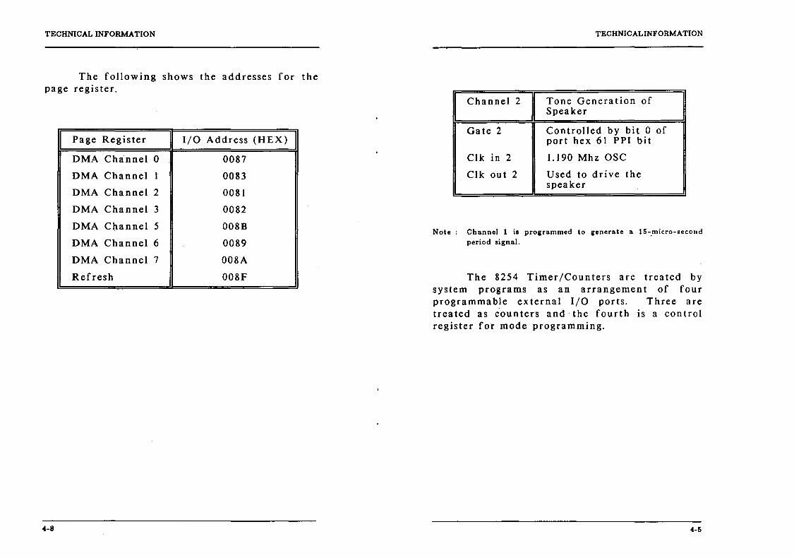
The following shows the addresses for the page register.
I Page Register I I/O Address (HEX)
DMA Channel 0 0087
DMA Channel 1 0083
DMA Channel 2 0081
DMA Channel 3 0082
DMA Channel 5 008B
DMA Channel 6 0089
DMA Channel 7 008A
Refresh 008F
4-8
TECHNICAL INFORMATION
Channel 2 Tone Genera tion of Speaker
Gate 2 Con trolled by bit 0 of port hex 61 PPI bit
Clk in 2 1.190 Mhz OSC
Clk out 2 Used to drive the speaker
Note: Channel I is programmed to generate a I5-micro-second
period signal.
The 8254 Timer/Counters are treated by system programs as an arrangement of four programmable external I/O ports. Three are treated as counters and the fourth is a control register for mode programming.
4-5
TECHNICAL INFORMATION
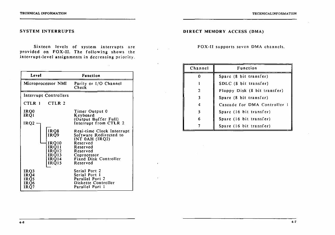
SYSTEM INTERRUPTS
Sixteen levels of system interrupts are provided on FOX-II. The following shows the interrupt-level assignments in decreasing priority.
Lnel Function
Microprocessor NMI Parity or I/O Channel Check
Interrupt Controllers
CTLR 1 CTLR 2
IRQO Timer Output 0 IRQI Keyboard
(Output Buffer Full) IRQ2 - Interrupt from CTLR 2
r--
IRQ8 Real-time Clock Interrupt IRQ9 Software Redirected to
INT OAH (IRQ2) '-- IRQIO Reserved
IRQII Reserved IRQI2 Reserved IRQ13 Coprocessor IRQI4 Fixed Disk Controller IRQI5 Reserved
L....-
IRQ3 Serial Port 2 IRQ4 Serial Port I IRQ5 Parallel Port 2 IRQ6 Diskette Controller IRQ? Parallel Port I
4-6
TECHNICAL INFORMATION
DIRECT MEMORY ACCESS (DMA)
FOX-II supports seven DMA channels.
Channel Function
0 Spare (8 bit transfer)
1 SDLC (8 bit transfer)
2 Floppy Disk (8 bit transfer)
3 Spare (8 bit transfer)
4 Cascade for DMA Con troller 1
5 Spare (16 bi t transfer)
6 Spare (16 bi t transfer)
? Spare (16 bi t transfer)
4-7

TECHNICAL INFORMATION
SYSTEM TIMERS
FOX-II has three programmable timer Icoun ters which are build-in in the chipset and they are defined as channels 0 through 2:
I Channel 0 I System Timer
Gate 0 Tied on
Clk in 0 1.190 Mhz OSC
Clk out 0 8259 IRQ 0
I Channel 1 I Refresh Request
I Generator
Gate 1 Tied on
Clk in 1 1.190 Mhz OSC
elk out 1 Request Refresh Cycle
TECHNICAL INFORMATION
REAL TIME CLOCK AND CMOS RAM
The CMOS RAM Chip (146818) contains the real-time clock and 64 bytes of CMOS RAM, it keeps configuration information when power is off. Upon you turn the system power on, CMOS will load the recorded configuration into the system so that the system can function in the right track with the equipped devices. However, if you haven't configured the CMOS, or the ba ttery which supports the power to the CMOS is weaken, you need to redefine the necessary parameters whenever the system is boot up. The following page shows the CMOS RAM addresses.

TECHNICAL INFORMATION
I/O ADDRESS MAP
I/O Address Map on System Board
I/O address hex 000 to OFF are reserved for the system board I/O.
ADDRESS DEVICE (HEX)
OOO-OIF DMA Controller I, 8237
020-03F Interrupt Controller I, 8259, Master
040-05F Timer, 8254
060-06F Keyboard Controller
070-07F Real Time Clock, NMI (non-maskable interrupt) mask
080-09F DMA Page Register, 74LS6I2
OAO-OBF Interrupt Controller 2, 8259
OCO-ODF DMA Controller 2, 8237
OFO Clear Math Coprocessor Busy
OFI Reset Math Coprocessor
OF8-0FF Math Coprocessor Port
4-2
TECHNICAL INFORMATION
REAL TIME CLOCK INFORMATION
The following table describes real-time clock bytes and specifies their addresses.
I Byte I Function Address
0 Seconds 00
I Second alarm 01
2 Minutes 02
3 Minute alarm 03
4 Hours 04
5 Hour alarm 05
6 Day of week 06
7 Da te of month 07
8 Month 08
9 Year 09
10 Status Register A OA
II Status Register B OB
12 Status Register C OC
13 Status Register D OD
4-11

INSTALLING COMPONBNTS
P 8 - External Battery Connector
Pin Assignment
1 + Vdc IT
2 not used 3 Ground 4 Ground
KB 1 - Keyboard Connector
Pin Assignmep.t
I Keyb01lrd .Crbc:~ "
2 Keyboard data 3 Spare 4 Ground 5 +5 Vdc
TECHN~ALINFORMATION
The following figure. shows the pin numbering for I/O channel connectors JAI-JA6.
81
810
820
831
REAR PANEL
J 1 1 1 1
" ,I 1 1 1 1 1 .I 1 1 1 1
:1 1 I. 1 , 1
, J 1 I
A1
A10
A20
A31
COMPONENT SIDE

INSTALLING COMPONENTS TECHNICAL INFORMATION
P 2 - Speaker Connector The following tables summarize pin assign men ts for the I/O cha nnel connectors.
Pin Assignmen t
1 Data out I/O Channel (A-Side)
2 +5 Vdc 3 Ground 4 +5 Vdc
I I/O Pin I Signal Name I I/O I Al -I/O CH CK I A2 SD7 I/O A3 SD6 I/O A4 SD5 I/O A5 SD4 I/O A6 SD3 I/O
P 3 - Turbo Switch Connector A7 SD2 I/O A8 SDI I/O A9 SDO I/O
AIO -I/O CH RDY I All AEN 0 Pin Assignment
1 Selection Pin A12 SA19 I/O A13 SA 18 I/O Al4 SA 17 I/O
2 Ground
A15 SA16 I/O A16 SA15 I/O A17 SA14 I/O A18 SA13 I/O A19 SA 12 I/O A20 SA 11 I/O P 4 - Turbo LED Connector
A21 SAI0 I/O A22 SA9 I/O
Pin Assignment A23 SA8 I/O
1 +5 Vdc 2 LED signal
A24 SA7 I/O A25 SA6 I/O A26 SA5 I/O A27 SA4 I/O A28 SA3 I/O A29 SA2 I/O A30 SAl I/O A31 SAO I/O
3-12 4-15
INSTALLING COMPONENTS
SYSTEM BOARD JUMPER SETTING
There are several jumpers in the motherboard tha t allow the user to select the desired system configuration. The following tables show the function and default settings of these jumpers.
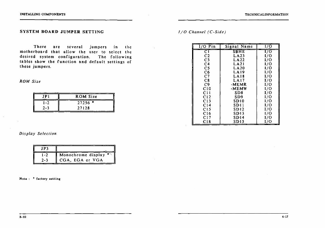
ROM Size
JPI ROM Size
1-2 27256 * 2-3 27128
Display Selection
I JP3 I 1-2 Monochrome display *", 2-3 eGA, EGA or VGA
Note: * factory setting
3-10
TECHNICAL INFORMATION
I/O Channel (C-Side)
I I/O Pin I Signal Name I I/O I CI SBHE I/O C2 LA23 I/O C3 LA22 I/O C4 LA21 I/O C5 LA20 I/O C6 LAI9 I/O C7 LAI8 I/O C8 LAI7 I/O C9 -MEMR I/O
CIO -MEMW I/O C II S08 I/O CI2 S09 I/O CI3 SOlO I/O CI4 SOlI I/O C 15 SOI2 I/O CI6 SOl3 I/O C 17 SOI4 I/O CI8 SOI5 I/O
4-17
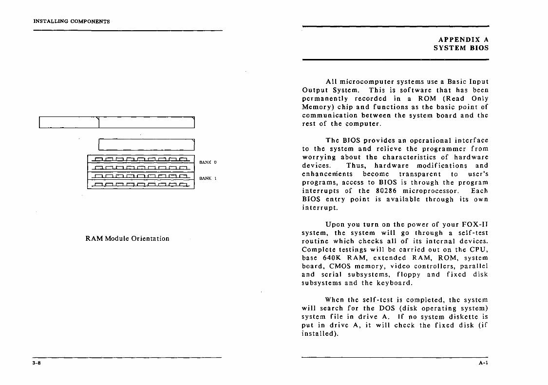
INSTALLING COMPONENTS
1 1
I 1
I iiiiiiii; I
RAM Module Orientation
3-8
BANK 0
BANK 1
APPENDIX A SYSTEM BIOS
All microcomputer systems use a Basic Input Output System. This is software that has been permanently recorded in a ROM (Read Only Memory) chip and functions as the basic point of communica tion between the system board and the rest of the computer.
The BIOS provides an operational interface to the system and relieve the programmer from worrying about the characteristics of hardware devices. Thus, hardware modifications and enhancements become transparent to user's programs, access to BIOS is through the program interrupts of the 80286 microprocessor. Each BIOS entry point is available through its own interrupt.
Upon you turn on the power of your FOX-II system, the system will go through a self-test routine which checks all of its internal devices. Complete testings will be carried out on the CPU, base 640K RAM, extended RAM, ROM, system board, CMOS memory, video controllers, parallel and serial subsystems, floppy and fixed disk su bsystems and the keyboard.
When the self -test is completed, the system will search for the DOS (disk operating system) system file in drive A. If no system diskette is put in drive A, it will check the fixed disk (if installed).
A-I
INSTALLING COMPONENTS
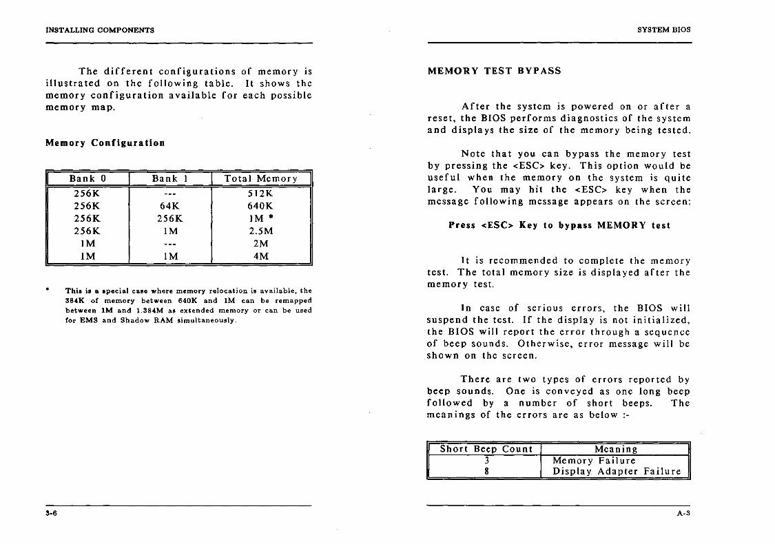
The different configurations of memory is illustrated on the following table. It shows the memory configuration available for each possible memory map.
Memory Configuration
•
3-6
Bank 0 Bank 1 Total Memory
256K --- 512K 256K 64K 640K 256K 256K 1M * 256K 1M 2.5M
1M --- 2M 1M 1M 4M
This is a special case where memory relocation is available, the 384K of memory between 640K and 1M can be remapped between 1M and 1.384M as extended memory or can be used for EMS and Shadow RAM simultaneously.
SYSTEM BIOS
MEMORY TEST BYPASS
After the system is powered on or after a reset, the BIOS performs diagnostics of the system and displa ys the size of the memory being tested.
Note that you can bypass the memory test by pressing the <ESC> key. This option would be useful when the memory on the system is quite large. You may hit the <ESC> key when the message following message appears on the screen:
Press <ESC> Key to bypass MEMORY test
It is recommended to complete the memory test. The total memory size is displayed after the memory test.
In case of serious errors, the BIOS will suspend the test. If the display is not initialized, the BIOS will report the error through a sequence of beep sounds. Otherwise, error message will be shown on the screen.
There are two types of errors reported by beep sounds. One is conveyed as one long beep followed by a number of short beeps. The meanings of the errors are as below :-
Short Beep Count Meaning 3 Memory Failure 8 Display Adapter Failure
A-3
INSTALLING COMPONENTS
SYSTEM MEMORY CONFIGURATION
FOX-II offers a flexible memory configuration. There are 2 memory banks a vaila ble, these memory banks are referenced as BANK 0 and BANK I in the motherboard. (See Appendix C for the motherboard layout) User has the option of either using DIP type DRAM or SIMM type memory modules. Still if the user prefers, he could use both types together. That means you could use DIP and SIMM type memory at the same time. Please note that however, you cannot install both memory types marked with the same bank reference. For example if you had already installed DIP memory into 'BANK 0', you can no longer install SIMM into the SIMM socket referenced as 'BANK 0'.
One bank of memory refers to as 2 SIMMs modules or 6 DIP memory chips (4x44256 + 2x41256). For the SIMM memory, user can install 256K and/or 1M SIMM; therefore it has a maximum memory capacity of 4 Megabytes. On the other hand; if purely DIP DRAM are used. it will allow up to I Megabytes of memory_ The DIP DRAM are organized in 2 banks as shown below:
3-4
SYSTEM BIOS
Do check the list to make sure that the configuration is correct. Sometimes, problems arise because of the incorrect information of the configuration. For example, if you forget to modify the setup after changing the floppy disk drive from one type to another, it can not boot from floppy disk or may not work properly. If you check the list, you can figure out the cause of the problem at the early stage.
A-5
INSTALLING COMPONENTS
Find the 80287 socket on your compu ter's system board. The socket has 20 holes on each side, and is located at 'U 12' on the corner of the motherboard.
Align the 80287 so that its notch matches up with the notch on the socket. Before you install the 80287, verify that its pins match up with the holes in the socket. If they don't, align the pins by laying the 80287 on its side on a table and gently pressing its top edge (not the pins). Repeat for the other row of pins.
When you are sure the pins are aligned correctly, press firmly and evenly on the 80287 to "seat" the pins in the socket. Carefully examin~ the 80287's pins. Look for any pins that are bent under or out. If you find bent pins, remove the 80287, gently straighten them, and insert the chip again.
3-2
SYSTEM BIOS
Use <Up> and <Down> keys to highligh t the selected item. Highlight RUN CMOS SETUP for the SETUP program and press the <Return> key to enter this option.
Depending on the BIOS version, a SETUP men u similar to below will appears:
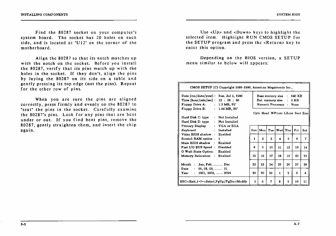
CMOS SETUP (C) Copyright 1985-1990, American Megatrends Inc.,
Date (mn/date/year) : Sun, Jul I, 1990 Base memory size : 640 KB Time (hour/min/sec) : 12 : 05 : 30 Ext. memory size : o KB Floppy Drive A: : 1.2 MB, 5¥." Numeric Processor : None Floppy Drive B: : 1.44 MB, 3'/,"
Cyln Head WPcom LZone Sect Size Hard Disk C: type : Not Installed Hard Disk D: type : Not Installed Primary Display : VGAor EGA Keyboard : Installed Sun Mon Tue Wed Thu Fri Sat Video BIOS shadow : Enabled Scratch RAM option : 1 1 2 3 4 5 6 7 Main BIOS shadow : Enabled Fast I/O BUS Speed: Disabled 8 9 10 11 12 13 14 o Wait State Option: Enabled Memory Relocation : Enabled 15 16 17 18 19 20 21
Month : Jan, Feb, .......... Dec 22 23 24 25 26 27 28 Date : 01,02,03, ........ 31 Year : 1901, 1902, ....... 2099 29 30 31 1 2 3 4
ESC=Exit,l .. t"=Select,PgUp/PgDn=Modify 5 6 7 8 9 10 11
A-7

GENERAL FEATURES
I/O SUBSYSTEM
It is very important that a high speed system should be compatible with existing peripherals without downgrading the performance. The FOX-II system is exactly designed with this capability in min4. It has the capability of communicating with I/O peripherals at 8MHz or slower while maintaining high speed for system operation.
SYSTEM FUNCTIONS
System functions include
Interrupt DMA Timer Real time clock Clock and ready generation I/O channel control
All system functions are 100% compatible to AT sta ndard. I/O channel of FOX-II is designed to be compa ti ble with standard AT bus. All the expansion cards conformed to the standard A T bus can be used in FOX-II without problem.
2-10
SYSTEM BIOS
Key Conventions
The field shown in reverse video is the current field, which is the one the user may changes.
Use the arrow keys to move the options. Use < PgUp> or < PgDn> to move bar inside settings menu. Use <ENTER> to select the options. Use <ESC> key to abort and· return to previous menu.
Note that if user settings do not allow system to startup, which happens if incorrect settings were made; the following steps should be taken:
a) Turn off the computer. b) Hold <INS> key down. c) Turn on the computer. d) When memory test begins, release <INS> key.
The above procedure will clear the CMOS register hence allowing the BIOS to bring up the system with BIOS default values.
A-9
GENERAL FEATURES
MEMORY SYSTEM
FOX-II features zero wait-state DRAM accesses in a design which supports up to 4 MByte of DRAM on the system board. This feature improve performance significantly relative to the conventional PC/ AT design. User can configure the DRAM for the one-wait/zero-wait option. This flexi bili ty in configuration allows you to select an ideal cost/performance combination.
Hardware LIM EMS is supported using 4 register sets for software applications which require expansion memory. Hardware EMS can also be disa bled allowing the use of software "Limulators" for maximum flexibility. Expanded memory provides usable memory beyond DOS's 640K limit. DOS application programs that conform to the EMS (such as the la test versions of 1-2-3, Symphony, Framework II, SuperCalc3) can use expanded memory. If you use DOS application programs, it would be most desirable to use EMS.
To further enhance the system performance, shadow RAM is supported. Shadow RAM is a technology that loads system BIOS and/or video BIOS from the low speed EPROM/ROM directly into fast DRAM during boot-up of the computer. The execution of the BIOS then will have significant improvement because access to DRAM is much faster than ROM.
BIOS is shadowed in 16K blocks in the range of COOOO to FFFFF. In the case that 1M of
2-8
SYSTEM BIOS
The BIOS is able to detect the type of the drives automatically. But remember to check the settings before exi t.
OPTION 3 FIXED DISK DRIVE
There are 47 types of fixed disks supported by the BIOS. Consult your fixed disk manual to determine its correct type. The parameters such as cylinder number, head number, sector number and pre-compensation must match your fixed disk's parameters.
Use PgUp and PgDn keys to change the fixed disk type. If the type of your fixed disk is not included in the hard disk list, define a new type as type 47. Use left and right arrow keys to move between the parameter fields and enter the parameters. The parameters will be stored in the CMOS RAM and your fixed disk can be used afterwards. Each hard disk can be assigned a different type 47 hard disk. So two hard disks which are not included in the list can be used together in your system.
If the type of fixed disk is wrong, it takes a while before the BIOS can identify the error. After setting the fixed disk type, if the system halts after reboot, please wait for a while. It is most likely that the setting of fixed disk type is incorrect.
A-ll

GENERAL FEATURES
MATH COPROCESSOR
The 80287 Math Coprocessor enables the FOX-II system to perform high-speed arithmetic, logarithmic functions, and trigonometric operations with extreme accuracy.
The coprocessor works in parallel with the microprocessor. The parallel operation decrease opera ting time by allowing the coprocessor to do rna thema tical calculations while the microprocessor continues to do other functions.
The 80287 Math Coprocessor is an extension to the 80286 microprocessor architecture. When combined with the 80286 microprocessor the 80287 dramatically increases the processing speed of computer application software which utilize mathematical operations. This makes an ideal compu ter workstation platform for applications such as financial modelling and spreadsheet, CAD/CAM, or graphics.
It adds over seventy mnemonics to the 80286 microprocessor instruction set. Specific 80287 math operations include logarithmic arithmetic, exponential, and trigonometric functions. The 80287 supports integer, extended integer, floating point and BCD data formats, and fully conforms to the ANSI/IEEE floating point standard.
The Mathematics Coprocessor, 80287 is treated as an I/O device through I/O port address hex OF8, OF A' and OFC. The microprocessor sends
2-6
SYSTEM BIOS
OPTION 5 KEYBOARD
If a keyboard is attached to the system, select 'Installed'. The BIOS will test the keyboard during self-test.
OPTION 6 VIDEO BIOS SHADOW
The Video BIOS Shadow can be enabled /disabled in this particular option. If the display card has no video ROM (as in the case of monochrome display card), there is no need to shadow the Video BIOS. However, if you are using VGA or EGA card where there's video ROM, video accesses will be improved if video BIOS shadow is enabled. You will not be able to enable this option if you have less than I MB of system memory.
a) Disabled * b) Enabled
A-13
GENERAL FEATURES
Virtual Address Mode
The virtual address mode provides a I-gigabyte virtual address space mapped onto a 16 megabyte physical address space. Virtual address space is larger than physical address space, and the use of a virtual address that does not map to a physical address location will cause a restartable in terrupt.
This mode uses 32-bit pointers that consist of a I6-bit selector and offset components. The selector specifies an index into a memory-residen t table, and the 24 bit base address of the desired segment is obtained from the memory table. A I6-bit offset is added to the segment base address to form the physical address. The microprocessor automatically references the tables whenever a segment register is loaded with a selector. Instructions that load a segment register will refer to the memory-based tables without additional program support. The memory-based tables contain 8-byte values called descriptors.
2-4
SYSTEM BIOS
OPTION 9 FAST I/O BUS SPEED
This option provides a way to speed up the I/O operation, however care should be exercised in setting this option. Make sure that the peripheral cards are capable of operating at high speed before making changes, otherwise problems could arise. It is therefore strongly recommended that this option be disabled.
a) Disabled * b) Enabled
OPTION 10 0 WAIT STATE OPTION
With this feature, user can use a wide range of DRAM speed a vaila ble. If the user is using slow DRAM, disable this option; this will provide better timing margins for the DRAM. If however high speed DRAM is available to the user, do enable this option; this will allow zero wait state memory access and improve the system performance significantly. In that way, it is up to the user to determine the desired cost/performance effective system.
a) Enabled * b) Disabled
A-I5

GENERAL FEATURES
I/O Subsystem:
Compatible to standard AT bus Four 16-bit expansion slots Two 8-bit expansion slots
System Support Functions:
8-Channel DMA (Direct Memory Access) 16-level interrupt 3 programmable timers CMOS RAM for system configuration Real time clock with battery backup OS/2 Optimization (Fast A20 gate and fast reset)
Other Features:
2-2
On board POWERGOOD test circuit External battery connector Hardware turbo switch
SYSTEM BIOS
EXITING CMOS SETUP
After you have en tered the correct val ues to all of the SETUP options, you may now exit the SETUP program. To do so, press <ESC> key to exit. The following message will then appear
Write data into CMOS and exit (Y /N)?
Press Y to update the data and exit the SETUP program.
The computer now performs a cold boot (equivalent to turning the power off and back on again), performs the memory test, and then tries to boot from the disk drive. If your hard disk has not yet been initialized, be sure that you have a boota ble DOS diskette in the A drive.
A-17
INTRODUCTION
To speed up the switching of CPU between protected and real mode, a special feature known as 'OS/2 Optimization' is also incorporated. Otherwise known as 'Hot Reset and Fast A20 Gate', this feature provides an unique method to handle the mode switching which will improve the performance for advanced operating system and expanded memory manager applications.
In addition, the FOX-II provides standard ISA expansion bus connectors so tha t add-on cards developed for the PC/AT will be fully functional. On-board power good genera tor is also implemented to ensure the reliability of the system and is capable of working with any power supplies.
FOX-II system is the perfect choice for general business spreadsheet, word presentation graphics, network workstations.
1-2
applications involving processing, database, telecommunica tions and
SYSTEM BIOS
Diagnostics Option Menu
You may note the following in the Diagnostics main menu:
The top line with title of the program, copyright message and the date and time in military format.
ROMDIAG Options Line with the devices/ adapters supported by the program. They are: Hard Disk, Floppy disk, Keyboard, Video and Misc. Each device option in the diagnostics option line has its own test option window which is displayed when the particular device is highlighted.
Diagnostics Option Window. Below the diagnostics option line, the diagnostics option menu for that option is displayed.
The Help Window in Reverse Video specifying usage of keys.
The bottom line with a short Message descri bing the test under the Block Cursor.
A-19
Chapter 4 TECHNICAL INFORMATION 4-1
Memory Mapping I/O Address Map System Timers System Interrupts
4-1 4-2 4-4 4-6
Direct Memory Access (DMA) 4-7 Real Time Clock and CMOS RAM 4-9 CMOS RAM Address Map 4-10 Real Time Clock In formation 4-11 System Expansion Bus 4-12
APPENDIX A SYSTEM BIOS
Memory Test Bypass CMOS Setup CMOS Setup Options Exiting CMOS Setup Running AMI BIOS Diagnostic
A-I
A-3 A-6
A-lO
A-17 A-IS
APPENDIX B OPERATION & MAINTENANCE B-1
Keeping the System Cool Cleaning the Golden Finger Cleaning the Motherboard
B-2 B-2 B-3
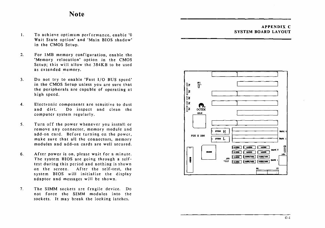
APPENDIX C SYSTEM BOARD LAYOUT C-1
APPENDIX B OPERATION AND MAINTENANCE
Some components of the FOX-II or computer components are static-sensitive devices and can be damaged by static discharges. To prevent such damage, the device may be wrapped in a conductive, anti-static bag; certain precautions should be taken before removing the device from its bags. When installing or removing any add-on card, DRAM module or coprocessor, care should be taken when handling these devices. Touch an unpaint metal part of your system unit (for example, the screws on the rear of the system unit) with one hand, then hold the component you are installing on the other hand. This will place your body, the component, and the system unit at the same ground potential, preventing an accidental static discharge. Be sure to handle circuit boards by the edges only and do not touch the component pins or solder Jowts. Grasp diskette drives or fixed disk drives by their frames to avoid touching the circuit board. Memory chips or co-processor should be held by their bodies only, not by their pins.
Preventing a problem is better than having to fix it after it has happened. This is where cleanliness and proper operating procedures come into play.
B-1
OPERATION AND MAINTENANCE
CLEANING THE MOTHERBOARD
Because the system is air-cooled, dust can enter your system through the ventilation slots. At least once a year, take the cover off your computer and vacuum the interior to remove accumulated dust. Use a brush attachment on the vacuum and carefully go over all exposed parts. To prevent dust from accumulating on the motherboard, installing all mounting plates on the rear of the case. Regularly examine your system, and if necessary, vacuum the interior of the system with a miniature vacuum.
B-3
Note
1. To achieve optimum performance, enable '0 Wait State option' and 'Main BIOS shadow' in the CMOS Setup.
2. For 1MB memory configuration, enable the 'Memory relocation' option in the CMOS Setup; this will allow the 384KB to be used as extended memory.
3.
4.
5.
6.
Do not try to enable 'Fast I/O BUS speed' in the CMOS Setup unless you are sure that the peripherals are capa ble of operating at high speed.
Electronic components are sensitive to dust and dirt. Do inspect and clean the compu ter system regular! y.
Turn off the power whenever you install or remove any connector, memory module and add-on card. Before turning on the power, make sure that all the connectors, memory mod ules and add-on cards are well secured.
After power is on, please wait for a minute. The system BIOS are going through a selftest during this period and nothing is shown on the screen. After the self-test, the system BIOS will initialize the display adaptor and messages will be shown.
7. The SIMM sockets are fragile dev ice. Do not force the SIMM modules into the sockets. It may break the locking latches.
~PI
0'
4't. OCTEK IITIII
D ~~H
FOX I 286
~m&eL
G II I
APPENDIX C SYSTEM BOARD LAYOUT
J
1 J
J J
I J
J J
1-'" BAlIK 1
pa
o KBl
C-l
The material in this manual iB for information only and is subject to change without notice.
REVISION: s.o
IBM, IBM PC/XT/AT, PC-DOS, MS-DOS, OS/2, UNIX, XENIX, INTEL, AMI ARE THE TRADEMARKS OR REGISTERED TRADEMARKS OF THEIR RESPECTIVE OWNERS.