flash in-system programmable (isp) peripherals for 8-bit ... sheets/st microelectronics...
TRANSCRIPT

1/111
NOT FOR NEW DESIGN
October 2008 Rev 5This is information on a product still in production but not recommended for new designs.
PSD813F1AFlash in-system programmable (ISP) peripherals
for 8-bit MCUs, 5 V
FEATURES SUMMARY■ DUAL BANK FLASH MEMORIES
– 1 Mbit of Primary Flash Memory (8 Uniform Sectors)
– 256 Kbit Secondary EEPROM (4 Uniform Sectors)
– Concurrent operation: read from one memory while erasing and writing the other
■ 16 Kbit SRAM ■ PLD WITH MACROCELLS
– Over 3,000 Gates Of PLD: DPLD and CPLD
– DPLD - User-defined Internal chip-select decoding
– CPLD with 16 Output Macrocells (OMCs) and 24 Input Macrocells (IMCs)
■ 27 RECONFIGURABLE I/Os– 27 individually configurable I/O port pins
that can be used for the following functions (16 I/O ports configurable as open-drain outputs):MCU I/OsPLD I/OsLatched MCU address output; andSpecial function I/Os
■ ENHANCED JTAG SERIAL PORT– Built-in JTAG-compliant serial port allows
full-chip In-System Programmability (ISP)– Efficient manufacturing allows for easy
product testing and programming■ PAGE REGISTER
– Internal page register that can be used to expand the microcontroller address space by a factor of 256.
■ PROGRAMMABLE POWER MANAGEMENT
Figure 1. Packages
■ HIGH ENDURANCE:– 100,000 Erase/WRITE Cycles of Flash
Memory– 10,000 Erase/WRITE Cycles of EEPROM– 1,000 Erase/WRITE Cycles of PLD– Data Retention: 15-year minimum at 90°C
(for Main Flash, Boot, PLD and Configuration bits).
■ SINGLE SUPPLY VOLTAGE:– 5V±10% for 5V
■ STANDBY CURRENT AS LOW AS 50µA■ Packages are ECOPACK®
PQFP52 (M)
PLCC52 (J)
TQFQ64 (U)

PSD813F1A
2/111
TABLE OF CONTENTS
Features Summary. . . . . . . . . . . . . . . . . . . . . . . . . . . . . . . . . . . . . . . . . . . . . . . . . . . . . . . . . . . . . . . . . 1
SUMMARY DESCRIPTION. . . . . . . . . . . . . . . . . . . . . . . . . . . . . . . . . . . . . . . . . . . . . . . . . . . . . . . . . . . 6
In-System Programming (ISP) via JTAG . . . . . . . . . . . . . . . . . . . . . . . . . . . . . . . . . . . . . . . . . . . . 6First time programming . . . . . . . . . . . . . . . . . . . . . . . . . . . . . . . . . . . . . . . . . . . . . . . . . . . . . . . . . . . 6Inventory build-up of pre-programmed devices . . . . . . . . . . . . . . . . . . . . . . . . . . . . . . . . . . . . . . . . . 6Expensive sockets. . . . . . . . . . . . . . . . . . . . . . . . . . . . . . . . . . . . . . . . . . . . . . . . . . . . . . . . . . . . . . . 6In-Application Programming (IAP). . . . . . . . . . . . . . . . . . . . . . . . . . . . . . . . . . . . . . . . . . . . . . . . . 6Simultaneous read and write to Flash memory . . . . . . . . . . . . . . . . . . . . . . . . . . . . . . . . . . . . . . . . . 6Complex memory mapping . . . . . . . . . . . . . . . . . . . . . . . . . . . . . . . . . . . . . . . . . . . . . . . . . . . . . . . . 6Separate program and data space . . . . . . . . . . . . . . . . . . . . . . . . . . . . . . . . . . . . . . . . . . . . . . . . . . 6PSDsoft Express . . . . . . . . . . . . . . . . . . . . . . . . . . . . . . . . . . . . . . . . . . . . . . . . . . . . . . . . . . . . . . . 6
PIN DESCRIPTION . . . . . . . . . . . . . . . . . . . . . . . . . . . . . . . . . . . . . . . . . . . . . . . . . . . . . . . . . . . . . . . . 10
PSD ARCHITECTURAL OVERVIEW . . . . . . . . . . . . . . . . . . . . . . . . . . . . . . . . . . . . . . . . . . . . . . . . . . 14
Memory. . . . . . . . . . . . . . . . . . . . . . . . . . . . . . . . . . . . . . . . . . . . . . . . . . . . . . . . . . . . . . . . . . . . . . 14PLDs . . . . . . . . . . . . . . . . . . . . . . . . . . . . . . . . . . . . . . . . . . . . . . . . . . . . . . . . . . . . . . . . . . . . . . . . 14I/O Ports . . . . . . . . . . . . . . . . . . . . . . . . . . . . . . . . . . . . . . . . . . . . . . . . . . . . . . . . . . . . . . . . . . . . . 14Microcontroller Bus Interface. . . . . . . . . . . . . . . . . . . . . . . . . . . . . . . . . . . . . . . . . . . . . . . . . . . . 14JTAG Port. . . . . . . . . . . . . . . . . . . . . . . . . . . . . . . . . . . . . . . . . . . . . . . . . . . . . . . . . . . . . . . . . . . . 15In-System Programming (ISP) . . . . . . . . . . . . . . . . . . . . . . . . . . . . . . . . . . . . . . . . . . . . . . . . . . . 15Page Register. . . . . . . . . . . . . . . . . . . . . . . . . . . . . . . . . . . . . . . . . . . . . . . . . . . . . . . . . . . . . . . . . 15Power Management Unit (PMU) . . . . . . . . . . . . . . . . . . . . . . . . . . . . . . . . . . . . . . . . . . . . . . . . . . 15
DEVELOPMENT SYSTEM . . . . . . . . . . . . . . . . . . . . . . . . . . . . . . . . . . . . . . . . . . . . . . . . . . . . . . . . . . 16
PSD Register Description and Address Offset . . . . . . . . . . . . . . . . . . . . . . . . . . . . . . . . . . . . . . . . . 17
DETAILED OPERATION. . . . . . . . . . . . . . . . . . . . . . . . . . . . . . . . . . . . . . . . . . . . . . . . . . . . . . . . . . . . 18
MEMORY BLOCKS . . . . . . . . . . . . . . . . . . . . . . . . . . . . . . . . . . . . . . . . . . . . . . . . . . . . . . . . . . . . 18Primary Flash Memory and Secondary EEPROM Description . . . . . . . . . . . . . . . . . . . . . . . . . 18Memory Block Select Signals . . . . . . . . . . . . . . . . . . . . . . . . . . . . . . . . . . . . . . . . . . . . . . . . . . . . . 18Ready/Busy Pin (PC3). . . . . . . . . . . . . . . . . . . . . . . . . . . . . . . . . . . . . . . . . . . . . . . . . . . . . . . . . . . 18Memory Operation. . . . . . . . . . . . . . . . . . . . . . . . . . . . . . . . . . . . . . . . . . . . . . . . . . . . . . . . . . . . . 19
INSTRUCTIONS . . . . . . . . . . . . . . . . . . . . . . . . . . . . . . . . . . . . . . . . . . . . . . . . . . . . . . . . . . . . . . . . . . 21
Power-down Instruction and Power-up Mode . . . . . . . . . . . . . . . . . . . . . . . . . . . . . . . . . . . . . . 21EEPROM Power Down Instruction . . . . . . . . . . . . . . . . . . . . . . . . . . . . . . . . . . . . . . . . . . . . . . . . . 21Power-up Mode . . . . . . . . . . . . . . . . . . . . . . . . . . . . . . . . . . . . . . . . . . . . . . . . . . . . . . . . . . . . . . . . 21READ . . . . . . . . . . . . . . . . . . . . . . . . . . . . . . . . . . . . . . . . . . . . . . . . . . . . . . . . . . . . . . . . . . . . . . . 22Read Memory Contents. . . . . . . . . . . . . . . . . . . . . . . . . . . . . . . . . . . . . . . . . . . . . . . . . . . . . . . . . . 22Read Main Flash Memory Identifier. . . . . . . . . . . . . . . . . . . . . . . . . . . . . . . . . . . . . . . . . . . . . . . . . 22Read Main Flash Memory Sector Protection Status . . . . . . . . . . . . . . . . . . . . . . . . . . . . . . . . . . . . 22
3/111
PSD813F1A
Reading the OTP Row. . . . . . . . . . . . . . . . . . . . . . . . . . . . . . . . . . . . . . . . . . . . . . . . . . . . . . . . . . . 22Reading the Erase/Program Status Bits . . . . . . . . . . . . . . . . . . . . . . . . . . . . . . . . . . . . . . . . . . . . . 22Data Polling Flag (DQ7). . . . . . . . . . . . . . . . . . . . . . . . . . . . . . . . . . . . . . . . . . . . . . . . . . . . . . . . . 23Toggle Flag (DQ6) . . . . . . . . . . . . . . . . . . . . . . . . . . . . . . . . . . . . . . . . . . . . . . . . . . . . . . . . . . . . . 23Error Flag (DQ5). . . . . . . . . . . . . . . . . . . . . . . . . . . . . . . . . . . . . . . . . . . . . . . . . . . . . . . . . . . . . . . 23Erase Time-out Flag DQ3 (Flash Memory only) . . . . . . . . . . . . . . . . . . . . . . . . . . . . . . . . . . . . . 23Writing to the EEPROM. . . . . . . . . . . . . . . . . . . . . . . . . . . . . . . . . . . . . . . . . . . . . . . . . . . . . . . . . 24Writing a Byte to EEPROM . . . . . . . . . . . . . . . . . . . . . . . . . . . . . . . . . . . . . . . . . . . . . . . . . . . . . . . 24Writing a Page to EEPROM . . . . . . . . . . . . . . . . . . . . . . . . . . . . . . . . . . . . . . . . . . . . . . . . . . . . . . 24EEPROM Software Data Protect (SDP) . . . . . . . . . . . . . . . . . . . . . . . . . . . . . . . . . . . . . . . . . . . . . 24Writing the OTP Row. . . . . . . . . . . . . . . . . . . . . . . . . . . . . . . . . . . . . . . . . . . . . . . . . . . . . . . . . . . 25
PROGRAMMING FLASH MEMORY. . . . . . . . . . . . . . . . . . . . . . . . . . . . . . . . . . . . . . . . . . . . . . . . . . . 27
Data Polling . . . . . . . . . . . . . . . . . . . . . . . . . . . . . . . . . . . . . . . . . . . . . . . . . . . . . . . . . . . . . . . . . . 27Data Toggle . . . . . . . . . . . . . . . . . . . . . . . . . . . . . . . . . . . . . . . . . . . . . . . . . . . . . . . . . . . . . . . . . . 28
ERASING FLASH MEMORY . . . . . . . . . . . . . . . . . . . . . . . . . . . . . . . . . . . . . . . . . . . . . . . . . . . . . . . . 29
Flash Bulk Erase . . . . . . . . . . . . . . . . . . . . . . . . . . . . . . . . . . . . . . . . . . . . . . . . . . . . . . . . . . . . . . 29Flash Sector Erase . . . . . . . . . . . . . . . . . . . . . . . . . . . . . . . . . . . . . . . . . . . . . . . . . . . . . . . . . . . . . 29Flash Erase Suspend . . . . . . . . . . . . . . . . . . . . . . . . . . . . . . . . . . . . . . . . . . . . . . . . . . . . . . . . . . 29Flash Erase Resume . . . . . . . . . . . . . . . . . . . . . . . . . . . . . . . . . . . . . . . . . . . . . . . . . . . . . . . . . . . 29
FLASH AND EEPROM MEMORY SPECIFIC FEATURES . . . . . . . . . . . . . . . . . . . . . . . . . . . . . . . . . 30
Flash Memory and EEPROM Sector Protect. . . . . . . . . . . . . . . . . . . . . . . . . . . . . . . . . . . . . . . . 30Reset. . . . . . . . . . . . . . . . . . . . . . . . . . . . . . . . . . . . . . . . . . . . . . . . . . . . . . . . . . . . . . . . . . . . . . . . 30
SRAM . . . . . . . . . . . . . . . . . . . . . . . . . . . . . . . . . . . . . . . . . . . . . . . . . . . . . . . . . . . . . . . . . . . . . . . . . . 30
MEMORY SELECT SIGNALS. . . . . . . . . . . . . . . . . . . . . . . . . . . . . . . . . . . . . . . . . . . . . . . . . . . . . . . . 31
Example . . . . . . . . . . . . . . . . . . . . . . . . . . . . . . . . . . . . . . . . . . . . . . . . . . . . . . . . . . . . . . . . . . . . . 31Memory Select Configuration for MCUs with Separate Program and Data Spaces . . . . . . . . 31Separate Space Modes . . . . . . . . . . . . . . . . . . . . . . . . . . . . . . . . . . . . . . . . . . . . . . . . . . . . . . . . . 32Combined Space Modes . . . . . . . . . . . . . . . . . . . . . . . . . . . . . . . . . . . . . . . . . . . . . . . . . . . . . . . . 32
PAGE REGISTER . . . . . . . . . . . . . . . . . . . . . . . . . . . . . . . . . . . . . . . . . . . . . . . . . . . . . . . . . . . . . . . . . 33
PLD’S . . . . . . . . . . . . . . . . . . . . . . . . . . . . . . . . . . . . . . . . . . . . . . . . . . . . . . . . . . . . . . . . . . . . . . . . . . 34
The Turbo Bit in PSD. . . . . . . . . . . . . . . . . . . . . . . . . . . . . . . . . . . . . . . . . . . . . . . . . . . . . . . . . . . 34
DECODE PLD (DPLD) . . . . . . . . . . . . . . . . . . . . . . . . . . . . . . . . . . . . . . . . . . . . . . . . . . . . . . . . . . . . . 36
COMPLEX PLD (CPLD) . . . . . . . . . . . . . . . . . . . . . . . . . . . . . . . . . . . . . . . . . . . . . . . . . . . . . . . . . . . . 37
Output Macrocell (OMC) . . . . . . . . . . . . . . . . . . . . . . . . . . . . . . . . . . . . . . . . . . . . . . . . . . . . . . . . 38Product Term Allocator. . . . . . . . . . . . . . . . . . . . . . . . . . . . . . . . . . . . . . . . . . . . . . . . . . . . . . . . . 39Loading and Reading the Output Macrocells (OMC). . . . . . . . . . . . . . . . . . . . . . . . . . . . . . . . . . . . 39The OMC Mask Register . . . . . . . . . . . . . . . . . . . . . . . . . . . . . . . . . . . . . . . . . . . . . . . . . . . . . . . . 39

PSD813F1A
4/111
The Output Enable of the OMC . . . . . . . . . . . . . . . . . . . . . . . . . . . . . . . . . . . . . . . . . . . . . . . . . . 39Input Macrocells (IMC) . . . . . . . . . . . . . . . . . . . . . . . . . . . . . . . . . . . . . . . . . . . . . . . . . . . . . . . . . 41
MCU BUS INTERFACE. . . . . . . . . . . . . . . . . . . . . . . . . . . . . . . . . . . . . . . . . . . . . . . . . . . . . . . . . . . . . 44
PSD Interface to a Multiplexed 8-Bit Bus . . . . . . . . . . . . . . . . . . . . . . . . . . . . . . . . . . . . . . . . . . 45PSD Interface to a Non-Multiplexed 8-Bit Bus . . . . . . . . . . . . . . . . . . . . . . . . . . . . . . . . . . . . . . 46Data Byte Enable Reference. . . . . . . . . . . . . . . . . . . . . . . . . . . . . . . . . . . . . . . . . . . . . . . . . . . . . 47MCU Bus Interface Examples. . . . . . . . . . . . . . . . . . . . . . . . . . . . . . . . . . . . . . . . . . . . . . . . . . . . 4780C31 . . . . . . . . . . . . . . . . . . . . . . . . . . . . . . . . . . . . . . . . . . . . . . . . . . . . . . . . . . . . . . . . . . . . . . . 4780C251 . . . . . . . . . . . . . . . . . . . . . . . . . . . . . . . . . . . . . . . . . . . . . . . . . . . . . . . . . . . . . . . . . . . . . . 4880C51XA . . . . . . . . . . . . . . . . . . . . . . . . . . . . . . . . . . . . . . . . . . . . . . . . . . . . . . . . . . . . . . . . . . . . . 5068HC11 . . . . . . . . . . . . . . . . . . . . . . . . . . . . . . . . . . . . . . . . . . . . . . . . . . . . . . . . . . . . . . . . . . . . . . 51
I/O PORTS. . . . . . . . . . . . . . . . . . . . . . . . . . . . . . . . . . . . . . . . . . . . . . . . . . . . . . . . . . . . . . . . . . . . . . . 52
General Port Architecture. . . . . . . . . . . . . . . . . . . . . . . . . . . . . . . . . . . . . . . . . . . . . . . . . . . . . . . 52Port Operating Modes . . . . . . . . . . . . . . . . . . . . . . . . . . . . . . . . . . . . . . . . . . . . . . . . . . . . . . . . . . 52MCU I/O Mode . . . . . . . . . . . . . . . . . . . . . . . . . . . . . . . . . . . . . . . . . . . . . . . . . . . . . . . . . . . . . . . . 54PLD I/O Mode . . . . . . . . . . . . . . . . . . . . . . . . . . . . . . . . . . . . . . . . . . . . . . . . . . . . . . . . . . . . . . . . . 54Address Out Mode. . . . . . . . . . . . . . . . . . . . . . . . . . . . . . . . . . . . . . . . . . . . . . . . . . . . . . . . . . . . . 54Address In Mode . . . . . . . . . . . . . . . . . . . . . . . . . . . . . . . . . . . . . . . . . . . . . . . . . . . . . . . . . . . . . . 56Data Port Mode . . . . . . . . . . . . . . . . . . . . . . . . . . . . . . . . . . . . . . . . . . . . . . . . . . . . . . . . . . . . . . . 56Peripheral I/O Mode. . . . . . . . . . . . . . . . . . . . . . . . . . . . . . . . . . . . . . . . . . . . . . . . . . . . . . . . . . . . 56JTAG In-System Programming (ISP) . . . . . . . . . . . . . . . . . . . . . . . . . . . . . . . . . . . . . . . . . . . . . . 57Port Configuration Registers (PCR) . . . . . . . . . . . . . . . . . . . . . . . . . . . . . . . . . . . . . . . . . . . . . . 57Control Register . . . . . . . . . . . . . . . . . . . . . . . . . . . . . . . . . . . . . . . . . . . . . . . . . . . . . . . . . . . . . . 57Direction Register . . . . . . . . . . . . . . . . . . . . . . . . . . . . . . . . . . . . . . . . . . . . . . . . . . . . . . . . . . . . . 58Drive Select Register. . . . . . . . . . . . . . . . . . . . . . . . . . . . . . . . . . . . . . . . . . . . . . . . . . . . . . . . . . . 58Port Data Registers . . . . . . . . . . . . . . . . . . . . . . . . . . . . . . . . . . . . . . . . . . . . . . . . . . . . . . . . . . . . 59Data In. . . . . . . . . . . . . . . . . . . . . . . . . . . . . . . . . . . . . . . . . . . . . . . . . . . . . . . . . . . . . . . . . . . . . . . 59Data Out Register . . . . . . . . . . . . . . . . . . . . . . . . . . . . . . . . . . . . . . . . . . . . . . . . . . . . . . . . . . . . . 59Output Macrocells (OMC) . . . . . . . . . . . . . . . . . . . . . . . . . . . . . . . . . . . . . . . . . . . . . . . . . . . . . . . 59Mask Macrocell Register. . . . . . . . . . . . . . . . . . . . . . . . . . . . . . . . . . . . . . . . . . . . . . . . . . . . . . . . 59Input Macrocells (IMC) . . . . . . . . . . . . . . . . . . . . . . . . . . . . . . . . . . . . . . . . . . . . . . . . . . . . . . . . . 59Enable Out . . . . . . . . . . . . . . . . . . . . . . . . . . . . . . . . . . . . . . . . . . . . . . . . . . . . . . . . . . . . . . . . . . . 60Ports A and B – Functionality and Structure . . . . . . . . . . . . . . . . . . . . . . . . . . . . . . . . . . . . . . . 60Port C – Functionality and Structure . . . . . . . . . . . . . . . . . . . . . . . . . . . . . . . . . . . . . . . . . . . . . . 61Port D – Functionality and Structure . . . . . . . . . . . . . . . . . . . . . . . . . . . . . . . . . . . . . . . . . . . . . . 62External Chip Select . . . . . . . . . . . . . . . . . . . . . . . . . . . . . . . . . . . . . . . . . . . . . . . . . . . . . . . . . . . 63
POWER MANAGEMENT . . . . . . . . . . . . . . . . . . . . . . . . . . . . . . . . . . . . . . . . . . . . . . . . . . . . . . . . . . . 64
Automatic Power-down (APD) Unit and Power-down Mode . . . . . . . . . . . . . . . . . . . . . . . . . . . 65Power-down Mode. . . . . . . . . . . . . . . . . . . . . . . . . . . . . . . . . . . . . . . . . . . . . . . . . . . . . . . . . . . . . 65For Users of the HC11 (or compatible) . . . . . . . . . . . . . . . . . . . . . . . . . . . . . . . . . . . . . . . . . . . . 66Other Power Saving Options . . . . . . . . . . . . . . . . . . . . . . . . . . . . . . . . . . . . . . . . . . . . . . . . . . . . 66PLD Power Management. . . . . . . . . . . . . . . . . . . . . . . . . . . . . . . . . . . . . . . . . . . . . . . . . . . . . . . . 66PSD Chip Select Input (CSI, PD2) . . . . . . . . . . . . . . . . . . . . . . . . . . . . . . . . . . . . . . . . . . . . . . . . 66
5/111
PSD813F1A
Input Clock . . . . . . . . . . . . . . . . . . . . . . . . . . . . . . . . . . . . . . . . . . . . . . . . . . . . . . . . . . . . . . . . . . . 66Input Control Signals . . . . . . . . . . . . . . . . . . . . . . . . . . . . . . . . . . . . . . . . . . . . . . . . . . . . . . . . . . 68
RESET TIMING AND DEVICE STATUS AT RESET . . . . . . . . . . . . . . . . . . . . . . . . . . . . . . . . . . . . . . 69
Power-On Reset. . . . . . . . . . . . . . . . . . . . . . . . . . . . . . . . . . . . . . . . . . . . . . . . . . . . . . . . . . . . . . . 69Warm Reset . . . . . . . . . . . . . . . . . . . . . . . . . . . . . . . . . . . . . . . . . . . . . . . . . . . . . . . . . . . . . . . . . . 69I/O Pin, Register and PLD Status at Reset . . . . . . . . . . . . . . . . . . . . . . . . . . . . . . . . . . . . . . . . . 69
PROGRAMMING IN-CIRCUIT USING THE JTAG SERIAL INTERFACE . . . . . . . . . . . . . . . . . . . . . . 71
Standard JTAG Signals. . . . . . . . . . . . . . . . . . . . . . . . . . . . . . . . . . . . . . . . . . . . . . . . . . . . . . . . . 71JTAG Extensions. . . . . . . . . . . . . . . . . . . . . . . . . . . . . . . . . . . . . . . . . . . . . . . . . . . . . . . . . . . . . . 72Security, Flash memory and EEPROM Protection . . . . . . . . . . . . . . . . . . . . . . . . . . . . . . . . . . . 72
INITIAL DELIVERY STATE. . . . . . . . . . . . . . . . . . . . . . . . . . . . . . . . . . . . . . . . . . . . . . . . . . . . . . . . . . 72
AC/DC PARAMETERS . . . . . . . . . . . . . . . . . . . . . . . . . . . . . . . . . . . . . . . . . . . . . . . . . . . . . . . . . . . . . 73
MAXIMUM RATING. . . . . . . . . . . . . . . . . . . . . . . . . . . . . . . . . . . . . . . . . . . . . . . . . . . . . . . . . . . . . . . . 76
DC AND AC PARAMETERS. . . . . . . . . . . . . . . . . . . . . . . . . . . . . . . . . . . . . . . . . . . . . . . . . . . . . . . . . 77
PACKAGE MECHANICAL . . . . . . . . . . . . . . . . . . . . . . . . . . . . . . . . . . . . . . . . . . . . . . . . . . . . . . . . . 100
PART NUMBERING . . . . . . . . . . . . . . . . . . . . . . . . . . . . . . . . . . . . . . . . . . . . . . . . . . . . . . . . . . . . . . 105
REVISION HISTORY. . . . . . . . . . . . . . . . . . . . . . . . . . . . . . . . . . . . . . . . . . . . . . . . . . . . . . . . . . . . . . 110

PSD813F1A
6/111
SUMMARY DESCRIPTIONThe PSD family of Programmable Microcontroller(MCU) Peripherals brings In-System Programma-bility (ISP) to Flash memory and programmablelogic. The result is a simple and flexible solution forembedded designs. PSD devices combine manyof the peripheral functions found in MCU basedapplications.PSD devices integrate an optimized “microcon-troller macrocell” logic architecture. The Macrocellwas created to address the unique requirementsof embedded system designs. It allows direct con-nection between the system address/data bus andthe internal PSD registers to simplify communica-tion between the MCU and other supporting devic-es.The PSD family offers two methods to programPSD Flash memory while the PSD is soldered to acircuit board.In-System Programming (ISP) via JTAGAn IEEE 1149.1 compliant JTAG interface is in-cluded on the PSD enabling the entire device(Flash memory, EEPROM, the PLD, and all con-figuration) to be rapidly programmed while sol-dered to the circuit board. This requires no MCUparticipation, which means the PSD can be pro-grammed anytime, even while completely blank.The innovative JTAG interface to Flash memoriesis an industry first, solving key problems faced bydesigners and manufacturing houses, such as:First time programming. How do I get firmwareinto the Flash the very first time? JTAG is the an-swer, program the PSD while blank with no MCUinvolvement.Inventory build-up of pre-programmed devic-es. How do I maintain an accurate count of pre-programmed Flash memory and PLD devicesbased on customer demand? How many and whatversion? JTAG is the answer, build your hardwarewith blank PSDs soldered directly to the board andthen custom program just before they are shippedto customer. No more labels on chips and no morewasted inventory.Expensive sockets. How do I eliminate the needfor expensive and unreliable sockets? JTAG is theanswer. Solder the PSD directly to the circuitboard. Program first time and subsequent timeswith JTAG. No need to handle devices and bendthe fragile leads.
In-Application Programming (IAP)Two independent memory arrays (Flash and EE-PROM) are included so the MCU can executecode from one memory while erasing and pro-gramming the other. Robust product firmware up-dates in the field are possible over anycommunication channel (CAN, Ethernet, UART,J1850, etc.) using this unique architecture. De-signers are relieved of these problems:Simultaneous read and write to Flash memo-ry. How can the MCU program the same memoryfrom which it is executing code? It cannot. ThePSD allows the MCU to operate the two memoriesconcurrently, reading code from one while erasingand programming the other during IAP.Complex memory mapping. I have only a 64K-byte address space to start with. How can I mapthese two memories efficiently? A ProgrammableDecode PLD is the answer. The concurrent PSDmemories can be mapped anywhere in MCU ad-dress space, segment by segment with extremelyhigh address resolution. As an option, the second-ary Flash memory can be swapped out of the sys-tem memory map when IAP is complete. A built-inpage register breaks the 64K-byte address limit.Separate program and data space. How can Iwrite to Flash or EEPROM memory while it residesin “program” space during field firmware updates,my MCU won’t allow it! The Flash PSD providesmeans to “reclassify” Flash or EEPROM memoryas “data” space during IAP, then back to “program”space when complete.PSDsoft ExpressPSDsoft Express, a software development toolfrom ST, guides you through the design processstep-by-step making it possible to complete anembedded MCU design capable of ISP/IAP in justhours. Select your MCU and PSDsoft Expresstakes you through the remainder of the design withpoint and click entry, covering PSD selection, pindefinitions, programmable logic inputs and out-puts, MCU memory map definition, ANSI-C codegeneration for your MCU, and merging your MCUfirmware with the PSD design. When complete,two different device programmers are supporteddirectly from PSDsoft Express: FlashLINK (JTAG)and PSDpro.
7/111
PSD813F1A
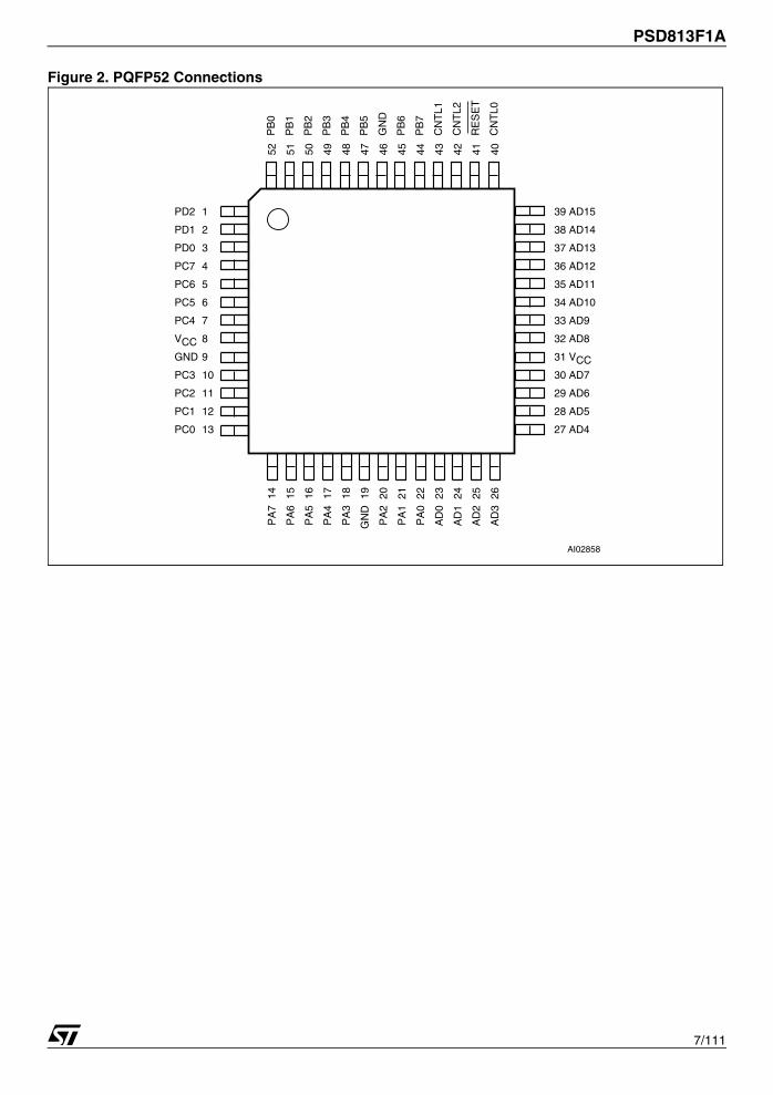
Figure 2. PQFP52 Connections
39 AD15
38 AD14
37 AD13
36 AD12
35 AD11
34 AD10
33 AD9
32 AD8
31 VCC30 AD7
29 AD6
28 AD5
27 AD4
PD2
PD1
PD0
PC7
PC6
PC5
PC4
VCCGND
PC3
PC2
PC1
PC0
1
2
3
4
5
6
7
8
9
10
11
12
13
52 51 50 49 48 47 46 45 44 43 42 41 40
PB
0
PB
1
PB
2
PB
3
PB
4
PB
5
GN
D
PB
6
PB
7
CN
TL1
CN
TL2
RE
SE
T
CN
TL0
14 15 16 17 18 19 20 21 22 23 24 25 26
PA
7
PA
6
PA
5
PA
4
PA
3
GN
D
PA
2
PA
1
PA
0
AD
0
AD
1
AD
2
AD
3
AI02858

PSD813F1A
8/111
Figure 3. PLCC52 Connections
PB0
PB1
PB2
PB3
PB4
PB5
GND
PB6
PB7
CNTL1
CNTL2
RESET
CNTL0
PA7
PA6
PA5
PA4
PA3
GND
PA2
PA1
PA0
AD0
AD1
AD2
AD3
AD15
AD14
AD13
AD12
AD11
AD10
AD9
AD8
VCC
AD7
AD6
AD5
AD4
PD2
PD1
PD0
PC7
PC6
PC5
PC4
VCC
GND
PC3
PC2
PC1
PC0
8
9
10
11
12
13
14
15
16
17
18
19
20
46
45
44
43
42
41
40
39
38
37
36
35
34
21
22
23
24
25
26
27
28
29
30
31
32
33
47
48
49
50
51
52
1
234567
AI02857
9/111
PSD813F1A
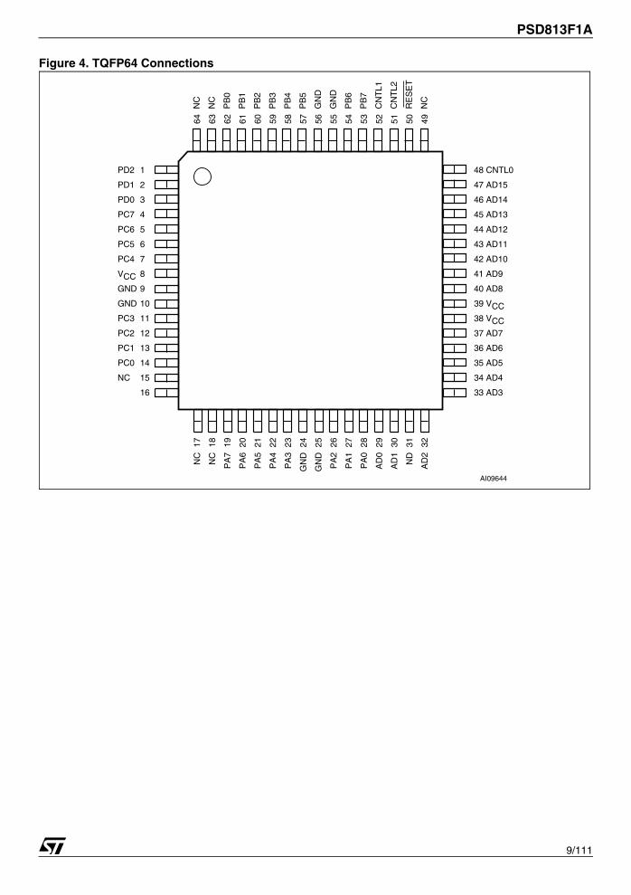
Figure 4. TQFP64 Connections
48 CNTL0
47 AD15
46 AD14
45 AD13
44 AD12
43 AD11
42 AD10
41 AD9
40 AD8
39 VCC38 VCC37 AD7
36 AD6
35 AD5
34 AD4
33 AD3
PD2
PD1
PD0
PC7
PC6
PC5
PC4
VCCGND
GND
PC3
PC2
PC1
PC0
NC
1
2
3
4
5
6
7
8
9
10
11
12
13
14
15
16
64 63 62 61 60 59 58 57 56 55 54 53 52 51 50 49
NC
NC
PB
0
PB
1
PB
2
PB
3
PB
4
PB
5
GN
D
GN
D
PB
6
PB
7
CN
TL1
CN
TL2
RE
SE
T
NC
17 18 19 20 21 22 23 24 25 26 27 28 29 30 31 32
NC
NC
PA
7
PA
6
PA
5
PA
4
PA
3
GN
D
GN
D
PA
2
PA
1
PA
0
AD
0
AD
1
ND
AD
2
AI09644
PSD813F1A
10/111
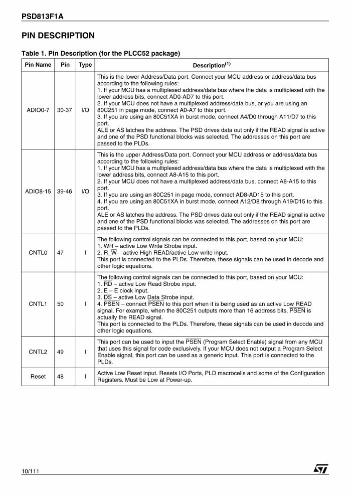
PIN DESCRIPTION
Table 1. Pin Description (for the PLCC52 package)
Pin Name Pin Type Description(1)
ADIO0-7 30-37 I/O
This is the lower Address/Data port. Connect your MCU address or address/data bus according to the following rules:1. If your MCU has a multiplexed address/data bus where the data is multiplexed with the lower address bits, connect AD0-AD7 to this port.2. If your MCU does not have a multiplexed address/data bus, or you are using an 80C251 in page mode, connect A0-A7 to this port.3. If you are using an 80C51XA in burst mode, connect A4/D0 through A11/D7 to this port.ALE or AS latches the address. The PSD drives data out only if the READ signal is active and one of the PSD functional blocks was selected. The addresses on this port are passed to the PLDs.
ADIO8-15 39-46 I/O
This is the upper Address/Data port. Connect your MCU address or address/data bus according to the following rules:1. If your MCU has a multiplexed address/data bus where the data is multiplexed with the lower address bits, connect A8-A15 to this port.2. If your MCU does not have a multiplexed address/data bus, connect A8-A15 to this port.3. If you are using an 80C251 in page mode, connect AD8-AD15 to this port.4. If you are using an 80C51XA in burst mode, connect A12/D8 through A19/D15 to this port.ALE or AS latches the address. The PSD drives data out only if the READ signal is active and one of the PSD functional blocks was selected. The addresses on this port are passed to the PLDs.
CNTL0 47 I
The following control signals can be connected to this port, based on your MCU:1. WR – active Low Write Strobe input.2. R_W – active High READ/active Low write input.This port is connected to the PLDs. Therefore, these signals can be used in decode and other logic equations.
CNTL1 50 I
The following control signals can be connected to this port, based on your MCU:1. RD – active Low Read Strobe input.2. E – E clock input.3. DS – active Low Data Strobe input.4. PSEN – connect PSEN to this port when it is being used as an active Low READ signal. For example, when the 80C251 outputs more than 16 address bits, PSEN is actually the READ signal.This port is connected to the PLDs. Therefore, these signals can be used in decode and other logic equations.
CNTL2 49 I
This port can be used to input the PSEN (Program Select Enable) signal from any MCU that uses this signal for code exclusively. If your MCU does not output a Program Select Enable signal, this port can be used as a generic input. This port is connected to the PLDs.
Reset 48 IActive Low Reset input. Resets I/O Ports, PLD macrocells and some of the Configuration Registers. Must be Low at Power-up.
11/111
PSD813F1A
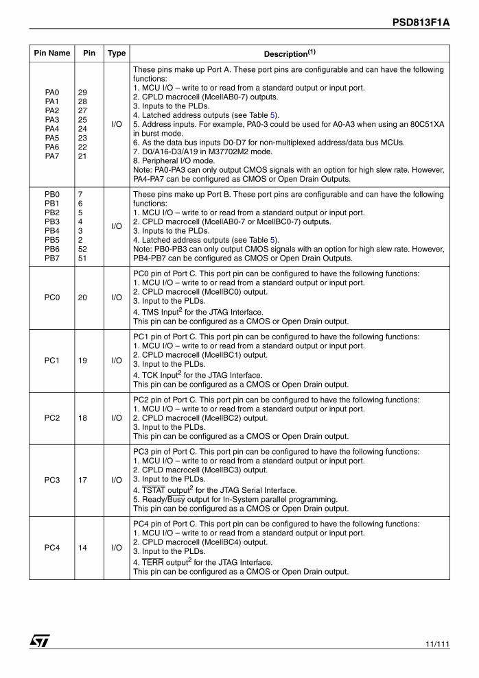
PA0PA1PA2PA3PA4PA5PA6PA7
2928272524232221
I/O
These pins make up Port A. These port pins are configurable and can have the following functions:1. MCU I/O – write to or read from a standard output or input port.2. CPLD macrocell (McellAB0-7) outputs.3. Inputs to the PLDs.4. Latched address outputs (see Table 5).5. Address inputs. For example, PA0-3 could be used for A0-A3 when using an 80C51XA in burst mode.6. As the data bus inputs D0-D7 for non-multiplexed address/data bus MCUs.7. D0/A16-D3/A19 in M37702M2 mode.8. Peripheral I/O mode.Note: PA0-PA3 can only output CMOS signals with an option for high slew rate. However, PA4-PA7 can be configured as CMOS or Open Drain Outputs.
PB0PB1PB2PB3PB4PB5PB6PB7
7654325251
I/O
These pins make up Port B. These port pins are configurable and can have the following functions:1. MCU I/O – write to or read from a standard output or input port.2. CPLD macrocell (McellAB0-7 or McellBC0-7) outputs.3. Inputs to the PLDs.4. Latched address outputs (see Table 5).Note: PB0-PB3 can only output CMOS signals with an option for high slew rate. However, PB4-PB7 can be configured as CMOS or Open Drain Outputs.
PC0 20 I/O
PC0 pin of Port C. This port pin can be configured to have the following functions:1. MCU I/O – write to or read from a standard output or input port.2. CPLD macrocell (McellBC0) output.3. Input to the PLDs.4. TMS Input2 for the JTAG Interface.This pin can be configured as a CMOS or Open Drain output.
PC1 19 I/O
PC1 pin of Port C. This port pin can be configured to have the following functions:1. MCU I/O – write to or read from a standard output or input port.2. CPLD macrocell (McellBC1) output.3. Input to the PLDs.4. TCK Input2 for the JTAG Interface.This pin can be configured as a CMOS or Open Drain output.
PC2 18 I/O
PC2 pin of Port C. This port pin can be configured to have the following functions:1. MCU I/O – write to or read from a standard output or input port.2. CPLD macrocell (McellBC2) output.3. Input to the PLDs.This pin can be configured as a CMOS or Open Drain output.
PC3 17 I/O
PC3 pin of Port C. This port pin can be configured to have the following functions:1. MCU I/O – write to or read from a standard output or input port.2. CPLD macrocell (McellBC3) output.3. Input to the PLDs.4. TSTAT output2 for the JTAG Serial Interface.5. Ready/Busy output for In-System parallel programming.This pin can be configured as a CMOS or Open Drain output.
PC4 14 I/O
PC4 pin of Port C. This port pin can be configured to have the following functions:1. MCU I/O – write to or read from a standard output or input port.2. CPLD macrocell (McellBC4) output.3. Input to the PLDs.4. TERR output2 for the JTAG Interface.This pin can be configured as a CMOS or Open Drain output.
Pin Name Pin Type Description(1)

PSD813F1A
12/111
Note: 1. The pin numbers in this table are for the PLCC package only. See the Figure 2., page 7, for pin numbers on other package type.2. These functions can be multiplexed with other functions.
PC5 13 I/O
PC5 pin of Port C. This port pin can be configured to have the following functions:1. MCU I/O – write to or read from a standard output or input port.2. CPLD macrocell (McellBC5) output.3. Input to the PLDs.4. TDI input2 for the JTAG Interface.This pin can be configured as a CMOS or Open Drain output.
PC6 12 I/O
PC6 pin of Port C. This port pin can be configured to have the following functions:1. MCU I/O – write to or read from a standard output or input port.2. CPLD macrocell (McellBC6) output.3. Input to the PLDs.4. TDO output2 for the JTAG Interface.This pin can be configured as a CMOS or Open Drain output.
PC7 11 I/O
PC7 pin of Port C. This port pin can be configured to have the following functions:1. MCU I/O – write to or read from a standard output or input port.2. CPLD macrocell (McellBC7) output.3. Input to the PLDs.4. DBE – active Low Data Byte Enable input from 68HC912 type MCUs.This pin can be configured as a CMOS or Open Drain output.
PD0 10 I/O
PD0 pin of Port D. This port pin can be configured to have the following functions:1. ALE/AS input latches address output from the MCU.2. MCU I/O – write or read from a standard output or input port.3. Input to the PLDs.4. CPLD output (External Chip Select).
PD1 9 I/O
PD1 pin of Port D. This port pin can be configured to have the following functions:1. MCU I/O – write to or read from a standard output or input port.2. Input to the PLDs.3. CPLD output (External Chip Select).4. CLKIN – clock input to the CPLD macrocells, the APD Unit’s Power-down counter, and the CPLD AND Array.
PD2 8 I/O
PD2 pin of Port D. This port pin can be configured to have the following functions:1. MCU I/O – write to or read from a standard output or input port.2. Input to the PLDs.3. CPLD output (External Chip Select).4. PSD Chip Select Input (CSI). When Low, the MCU can access the PSD memory and I/O. When High, the PSD memory blocks are disabled to conserve power.
VCC 15, 38 Supply Voltage
GND1, 16, 26 Ground pins
Pin Name Pin Type Description(1)
13/111
PSD813F1A
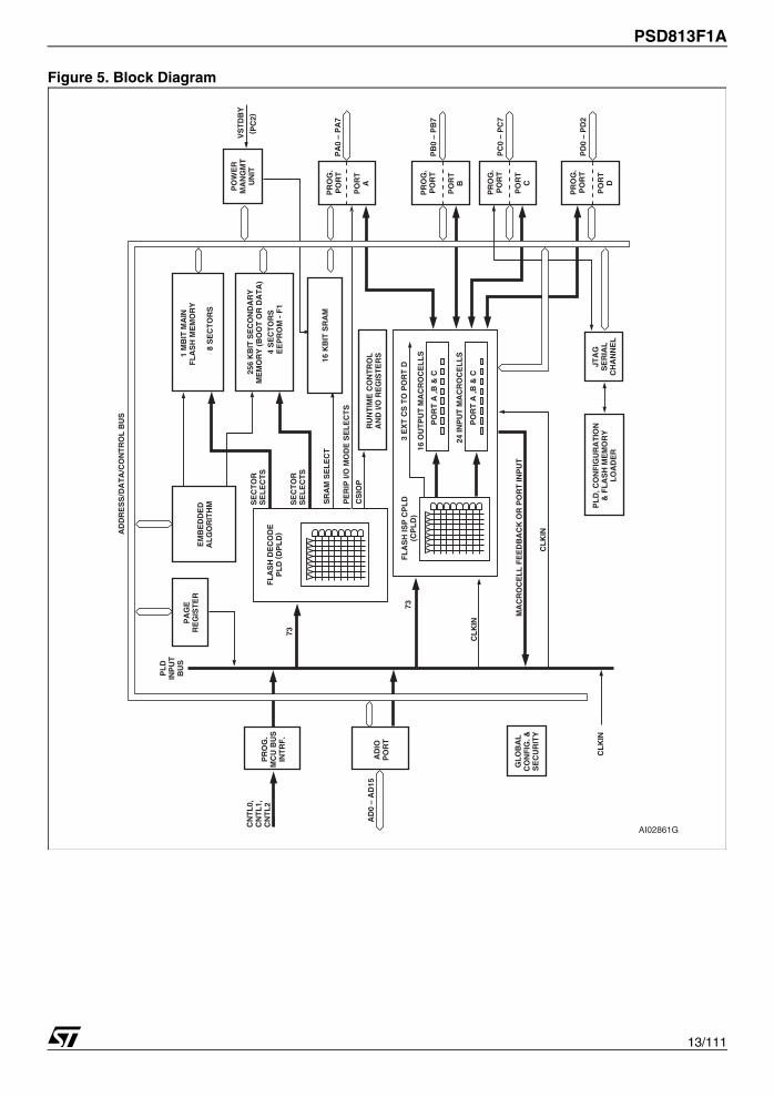
Figure 5. Block Diagram
PR
OG
.M
CU
BU
SIN
TR
F.
AD
IOP
OR
T
CN
TL
0,C
NT
L1,
CN
TL
2
AD
0 –
AD
15
CL
KIN
CL
KIN
CL
KIN
PL
DIN
PU
TB
US
PR
OG
.P
OR
T
PO
RT
A
PR
OG
.P
OR
T
PO
RT
B
PO
WE
RM
AN
GM
TU
NIT
1 M
BIT
MA
INF
LA
SH
ME
MO
RY
8 S
EC
TO
RS
VS
TD
BY
PA
0 –
PA
7
PB
0 –
PB
7
PR
OG
.P
OR
T
PO
RT
C
PR
OG
.P
OR
T
PO
RT
D
PC
0 –
PC
7
PD
0 –
PD
2
AD
DR
ES
S/D
AT
A/C
ON
TR
OL
BU
S
PO
RT
A ,B
& C
3 E
XT
CS
TO
PO
RT
D
24 IN
PU
T M
AC
RO
CE
LL
S
PO
RT
A ,B
& C
73
73
256
KB
IT S
EC
ON
DA
RY
ME
MO
RY
(B
OO
T O
R D
AT
A)
4 S
EC
TO
RS
EE
PR
OM
- F
1
16 K
BIT
SR
AM
RU
NT
IME
CO
NT
RO
LA
ND
I/O
RE
GIS
TE
RS
SR
AM
SE
LE
CT
PE
RIP
I/O
MO
DE
SE
LE
CT
S
MA
CR
OC
EL
L F
EE
DB
AC
K O
R P
OR
T IN
PU
T
CS
IOP
FL
AS
H IS
P C
PL
D(C
PL
D)
16 O
UT
PU
T M
AC
RO
CE
LL
S
FL
AS
H D
EC
OD
EP
LD
(D
PL
D)
PL
D, C
ON
FIG
UR
AT
ION
& F
LA
SH
ME
MO
RY
LO
AD
ER
JTA
GS
ER
IAL
CH
AN
NE
L
( PC
2)
PA
GE
RE
GIS
TE
RE
MB
ED
DE
DA
LG
OR
ITH
M SE
CT
OR
SE
LE
CT
S
SE
CT
OR
SE
LE
CT
S
GL
OB
AL
CO
NF
IG. &
SE
CU
RIT
Y
AI02861G
PSD813F1A
14/111
PSD ARCHITECTURAL OVERVIEWPSD devices contain several major functionalblocks. Figure 5 shows the architecture of the PSDdevice. The functions of each block are describedbriefly in the following sections. Many of the blocksperform multiple functions and are user configu-rable.MemoryThe PSD contains the following memories:■ a 1 Mbit Flash memory■ a secondary 256 Kbit EEPROM memory■ a 16 Kbit SRAMEach of the memory blocks is briefly discussed inthe following paragraphs. A more detailed discus-sion can be found in the section entitled MEMORYBLOCKS, page 18.The 1 Mbit Flash memory is the main memory ofthe PSD. It is divided into 8 equally-sized sectorsthat are individually selectable.The 256 Kbit EEPROM or Flash memory is dividedinto 4 equally-sized sectors. Each sector is individ-ually selectable.The 16 Kbit SRAM is intended for use as ascratchpad memory or as an extension to the mi-crocontroller SRAM. Each sector of memory can be located in a differ-ent address space as defined by the user. The ac-cess times for all memory types includes theaddress latching and DPLD decoding time.PLDsThe device contains two PLD blocks, each opti-mized for a different function, as shown in Table 2.The functional partitioning of the PLDs reducespower consumption, optimizes cost/performance,and eases design entry.The Decode PLD (DPLD) is used to decode ad-dresses and generate chip selects for the PSD in-ternal memory and registers. The CPLD canimplement user-defined logic functions. The DPLDhas combinatorial outputs. The CPLD has 16 Out-put macrocells and 3 combinatorial outputs. ThePSD also has 24 Input macrocells that can be con-figured as inputs to the PLDs. The PLDs receivetheir inputs from the PLD Input Bus and are differ-entiated by their output destinations, number ofProduct Terms, and macrocells.
The PLDs consume minimal power by using Zero-Power design techniques. The speed and powerconsumption of the PLD is controlled by the TurboBit (ZPSD only) in the PMMR0 register and otherbits in the PMMR2 registers. These registers areset by the microcontroller at runtime. There is aslight penalty to PLD propagation time when in-voking the ZPSD features.I/O PortsThe PSD has 27 I/O pins divided among four ports(Port A, B, C, and D). Each I/O pin can be individ-ually configured for different functions. Ports A, B,C and D can be configured as standard MCU I/Oports, PLD I/O, or latched address outputs for mi-crocontrollers using multiplexed address/databusses.The JTAG pins can be enabled on Port C for In-System Programming (ISP).Ports A and B can also be configured as a dataport for a n on-multiplexed bus or multiplexed Ad-dress/Data buses for certain types of 16-bit micro-controllers.Microcontroller Bus InterfaceThe PSD easily interfaces with most 8-bit micro-controllers that have either multiplexed or non-multiplexed address/data busses. The device isconfigured to respond to the microcontroller’s con-trol signals, which are also used as inputs to thePLDs. Where there is a requirement to use a 16-bit data bus to interface to a 16-bit microcontroller,two PSDs must be used. For examples, pleasesee the section entitled MCU Bus InterfaceExamples, page 47.
Table 2. PLD I/O
Name Inputs Outputs Product Terms
Decode PLD (DPLD) 73 17 42
Complex PLD (CPLD) 73 19 140
15/111
PSD813F1A
JTAG PortIn-System Programming can be performedthrough the JTAG pins on Port C. This serial inter-face allows complete programming of the entirePSD device. A blank device can be completelyprogrammed. The JTAG signals (TMS, TCK,TSTAT, TERR, TDI, TDO) can be multiplexed withother functions on Port C. Table 3 indicates theJTAG signals pin assignments.In-System Programming (ISP)Using the JTAG signals on Port C, the entire PSDdevice can be programmed or erased without theuse of the microcontroller. The main Flash memo-ry can also be programmed in-system by the mi-crocontroller executing the programmingalgorithms out of the EEPROM or SRAM. The EE-PROM can be programmed the same way by exe-cuting out of the main Flash memory. The PLDlogic or other PSD configuration can be pro-grammed through the JTAG port or a device pro-grammer. Table 4 indicates which programmingmethods can program different functional blocksof the PSD.Page RegisterThe 8-bit Page Register expands the addressrange of the microcontroller by up to 256 times.The paged address can be used as part of the ad-dress space to access external memory and pe-ripherals, or internal memory and I/O. The PageRegister can also be used to change the addressmapping of blocks of Flash memory into differentmemory spaces for in-circuit programming.
Power Management Unit (PMU)The Power Management Unit (PMU) in the PSDgives the user control of the power consumptionon selected functional blocks based on system re-quirements. The PMU includes an Automatic Pow-er Down unit (APD) that will turn off devicefunctions due to microcontroller inactivity. TheAPD unit has a Power Down Mode that helps re-duce power consumption.The PSD also has some bits that are configured atrun-time by the MCU to reduce power consump-tion of the CPLD. The turbo bit in the PMMR0 reg-ister can be turned off and the CPLD will latch itsoutputs and go to sleep until the next transition onits inputs. Additionally, bits in the PMMR2 register can be setby the MCU to block signals from entering theCPLD to reduce power consumption. Please seethe section entitled POWERMANAGEMENT, page 64 for more details.
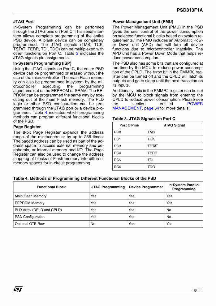
Table 3. JTAG SIgnals on Port C
Table 4. Methods of Programming Different Functional Blocks of the PSD
Port C Pins JTAG Signal
PC0 TMS
PC1 TCK
PC3 TSTAT
PC4 TERR
PC5 TDI
PC6 TDO
Functional Block JTAG Programming Device Programmer In-System Parallel Programming
Main Flash Memory Yes Yes Yes
EEPROM Memory Yes Yes Yes
PLD Array (DPLD and CPLD) Yes Yes No
PSD Configuration Yes Yes No
Optional OTP Row No Yes Yes
PSD813F1A
16/111
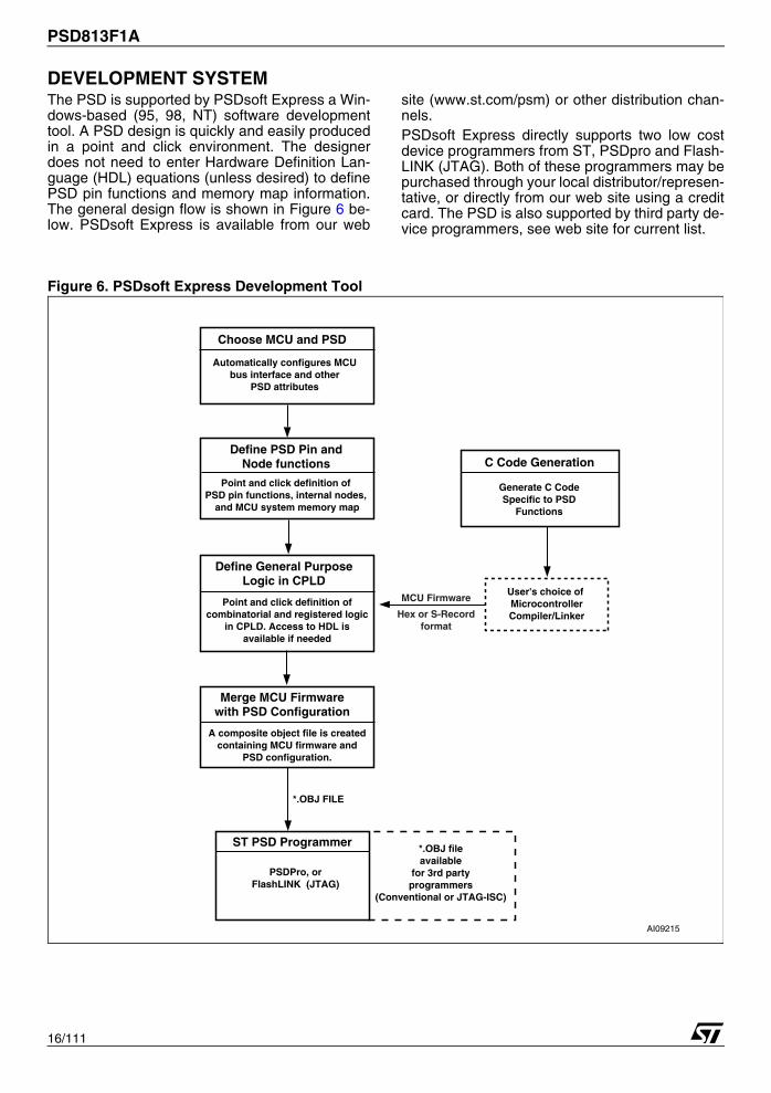
DEVELOPMENT SYSTEMThe PSD is supported by PSDsoft Express a Win-dows-based (95, 98, NT) software developmenttool. A PSD design is quickly and easily producedin a point and click environment. The designerdoes not need to enter Hardware Definition Lan-guage (HDL) equations (unless desired) to definePSD pin functions and memory map information.The general design flow is shown in Figure 6 be-low. PSDsoft Express is available from our web
site (www.st.com/psm) or other distribution chan-nels.PSDsoft Express directly supports two low costdevice programmers from ST, PSDpro and Flash-LINK (JTAG). Both of these programmers may bepurchased through your local distributor/represen-tative, or directly from our web site using a creditcard. The PSD is also supported by third party de-vice programmers, see web site for current list.
Figure 6. PSDsoft Express Development Tool
Define PSD Pin andNode functions
Define General PurposeLogic in CPLD
ST PSD Programmer
*.OBJ FILE
Point and click definition of PSD pin functions, internal nodes,
and MCU system memory map
PSDPro, orFlashLINK (JTAG)
Point and click definition ofcombinatorial and registered logic
in CPLD. Access to HDL isavailable if needed
Choose MCU and PSD
Automatically configures MCUbus interface and other
PSD attributes
C Code Generation
Generate C CodeSpecific to PSD
Functions
User's choice of MicrocontrollerCompiler/Linker
*.OBJ fileavailable
for 3rd partyprogrammers
(Conventional or JTAG-ISC)
MCU Firmware
Hex or S-Recordformat
AI09215
Merge MCU Firmwarewith PSD Configuration
A composite object file is createdcontaining MCU firmware and
PSD configuration.
17/111
PSD813F1A
PSD REGISTER DESCRIPTION AND ADDRESS OFFSETTable 5 shows the offset addresses to the PSDregisters relative to the CSIOP base address. TheCSIOP space is the 256 bytes of address that is al-located by the user to the internal PSD registers.
Table 6 provides brief descriptions of the registersin CSIOP space. The following section gives amore detailed description.
Table 5. I/O Port Latched Address Output Assignments
Note: 1. See the section entitled I/O PORTS, page 52, on how to enable the Latched Address Output function.2. N/A = Not Applicable
Table 6. Register Address Offset
Note: 1. Other registers that are not part of the I/O ports.
MCU(1) Port A(2) Port B(2)
Port A (3:0) Port A (7:4) Port B (3:0) Port B (7:4)
8051XA (8-bit) N/A Address a7-a4 Address a11-a8 N/A
80C251 (page mode) N/A N/A Address a11-a8 Address a15-a12
All other 8-bit multiplexed Address a3-a0 Address a7-a4 Address a3-a0 Address a7-a4
8-bit non-multiplexed bus N/A N/A Address a3-a0 Address a7-a4
Register Name Port A
Port B
Port C
Port D Other(1) Description
Data In 00 01 10 11 Reads Port pin as input, MCU I/O input mode
Control 02 03 Selects mode between MCU I/O or Address Out
Data Out 04 05 12 13 Stores data for output to Port pins, MCU I/O output mode
Direction 06 07 14 15 Configures Port pin as input or output
Drive Select 08 09 16 17 Configures Port pins as either CMOS or Open Drain on some pins, while selecting high slew rate on other pins.
Input Macrocell 0A 0B 18 Reads Input Macrocells
Enable Out 0C 0D 1A 1B Reads the status of the output enable to the I/O Port driver
Output Macrocells AB 20 20 READ – reads output of macrocells AB
WRITE – loads macrocell flip-flops
Output Macrocells BC
21 21 READ – reads output of macrocells BCWRITE – loads macrocell flip-flops
Mask Macrocells AB 22 22 Blocks writing to the Output Macrocells AB
Mask Macrocells BC 23 23 Blocks writing to the Output Macrocells BC
Primary Flash Protection
C0 Read only – Flash Sector Protection
Secondary Flash memory Protection
C2 Read only – PSD Security and EEPROM Sector Protection
JTAG Enable C7 Enables JTAG Port
PMMR0 B0 Power Management Register 0
PMMR2 B4 Power Management Register 2
Page E0 Page Register
VM E2 Places PSD memory areas in Program and/or Data space on an individual basis.
PSD813F1A
18/111
DETAILED OPERATIONAs shown in Figure 5., page 13, the PSD consistsof six major types of functional blocks:■ Memory Blocks■ PLD Blocks■ MCU Bus Interface■ I/O Ports■ Power Management Unit (PMU)■ JTAG InterfaceThe functions of each block are described in thefollowing sections. Many of the blocks performmultiple functions, and are user configurable.MEMORY BLOCKSThe PSD has the following memory blocks (seeTable 7):– The Main Flash memory– Secondary EEPROM memory– SRAMThe Memory Select signals for these blocks origi-nate from the Decode PLD (DPLD) and are user-defined in PSDsoft Express.Primary Flash Memory and Secondary EEPROM DescriptionThe 1Mb primary Flash memory is divided evenlyinto eight 16-KByte sectors. The EEPROM memo-ry is divided into four sectors of eight KBytes each.Each sector of either memory can be separatelyprotected from Program and Erase operations.Flash memory may be erased on a sector-by-sec-tor basis and programmed byte-by-byte. Flashsector erasure may be suspended while data isread from other sectors of memory and then re-sumed after reading.EEPROM may be programmed byte-by-byte orsector-by-sector, and erasing is automatic and
transparent. The integrity of the data can be se-cured with the help of Software Data Protection(SDP). Any write operation to the EEPROM is in-hibited during the first five milliseconds followingpower-up.During a program or erase of Flash, or during awrite of the EEPROM, the status can be output onthe Ready/Busy (PC3) pin of Port C3. This pin isset up using PSDsoft Express Configuration.Memory Block Select Signals. The decodePLD in the PSD generates the chip selects for allthe internal memory blocks (refer to the sectionentitled PLD’S, page 34). Each of the eight Flashmemory sectors have a Flash Select signal (FS0-FS7) which can contain up to three product terms.Each of the four EEPROM memory sectors have aSelect signal (EES0-3 or CSBOOT0-3) which cancontain up to three product terms. Having threeproduct terms for each sector select signal allowsa given sector to be mapped in different areas ofsystem memory. When using a microcontrollerwith separate Program and Data space, theseflexible select signals allow dynamic re-mapping ofsectors from one space to the other.Ready/Busy Pin (PC3). Pin PC3 can be used tooutput the Ready/Busy status of the PSD. The out-put on the pin will be a ‘0’ (Busy) when Flash orEEPROM memory blocks are being written to, orwhen the Flash memory block is being erased.The output will be a ‘1’ (Ready) when no write orerase operation is in progress.
Table 7. Memory Blocks
Device Main Flash EEPROM SRAM
PSD813F1A 128KB 32KB 2KB
19/111
PSD813F1A
Memory OperationThe main Flash and EEPROM memory are ad-dressed through the microcontroller interface onthe PSD device. The microcontroller can accessthese memories in one of two ways:– The microcontroller can execute a typical bus
WRITE or READ operation just as it would if accessing a RAM or ROM device using standard bus cycles.
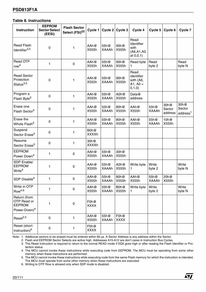
– The microcontroller can execute a specific instruction that consists of several WRITE and READ operations. This involves writing specific data patterns to special addresses within the Flash or EEPROM to invoke an embedded algorithm. These instructions are summarized in Table 8., page 20.
Typically, Flash memory can be read by the micro-controller using READ operations, just as it wouldread a ROM device. However, Flash memory canonly be erased and programmed with specific in-structions. For example, the microcontroller can-not write a single byte directly to Flash memory asone would write a byte to RAM. To program a byte
into Flash memory, the microcontroller must exe-cute a program instruction sequence, then test thestatus of the programming event. This status testis achieved by a READ operation or polling theReady/Busy pin (PC3).The Flash memory can also be read by using spe-cial instructions to retrieve particular Flash deviceinformation (sector protect status and ID).The EEPROM is a bit different. Data can be writtento EEPROM memory using write operations, likewriting to a RAM device, but the status of eachWRITE event must be checked by the microcon-troller. A WRITE event can be one to 64 contigu-ous bytes. The status test is very similar to thatused for Flash memory (READ operation orReady/Busy). Optionally, the EEPROM memorymay be put into a Software Data Protect (SDP)mode where it requires instructions, rather thanoperations, to alter its contents. SDP mode makeswriting to EEPROM much like writing to Flashmemory.
PSD813F1A
20/111
Table 8. Instructions
Note: 1. Additional sectors to be erased must be entered within 80 µs. A Sector Address is any address within the Sector.2. Flash and EEPROM Sector Selects are active high. Addresses A15-A12 are don’t cares in Instruction Bus Cycles.3. The Reset instruction is required to return to the normal READ mode if DQ5 goes high or after reading the Flash Identifier or Pro-
tection status.4. The MCU cannot invoke these instructions while executing code from EEPROM. The MCU must be operating from some other
memory when these instructions are performed.5. The MCU cannot invoke these instructions while executing code from the same Flash memory for which the instruction is intended.
The MCU must operate from some other memory when these instructions are executed.6. Writing to OTP Row is allowed only when SDP mode is disabled.
InstructionEEPROM
Sector Select (EESi)
Flash Sector Select (FSi)(2) Cycle 1 Cycle 2 Cycle 3 Cycle 4 Cycle 5 Cycle 6 Cycle 7
Read Flash Identifier3,5 0 1
AAh@ X555h
55h@ XAAAh
90h@ X555h
Read Identifier with (A6,A1,A0 at 0,0,1)
Read OTP row4 1 0 AAh@
X555h55h@ XAAAh
90h@ X555h
Read byte 1
Read byte 2
Read byte N
Read Sector Protection Status3,5
0 1 AAh@ X555h
55h@ XAAAh
90h@ X555h
Read identifier with (A6, A1; A0 = 0,1,0)
Program a Flash Byte5 0 1 AAh@
X555h55h@ XAAAh
A0h@ X555h
Data@ address
Erase one Flash Sector5
0 1 AAh@ X555h
55h@ XAAAh
80h@ X555h
AAh@ X555h
55h@ XAAAh
30h@ Sector address
30h@ Sector address1
Erase the Whole Flash5 0 1 AAh@
X555h55h@ XAAAh
80h@ X555h
AAh@ X555h
55h@ XAAAh
10h@ X555h
Suspend Sector Erase5 0 1
B0h@ XXXXh
Resume Sector Erase5 0 1 30h@
XXXXh
EEPROM Power Down4 1 0
AAh@ X555h
55h@ XAAAh
30h@ X555h
SDP Enable/EEPROM Write4
1 0AAh@ X555h
55h@ XAAAh
A0h@ X555h
Write byte 1
Write byte 2
Write byte N
SDP Disable4 1 0 AAh@ X555h
55h@ XAAAh
80h@ X555h
AAh@ X555h
55h@ XAAAh
20h@ X555h
Write in OTP Row4,6 1 0 AAh@
X555h55h@ XAAAh
B0h@ X555h
Write byte 1
Write byte 2
Write byte N
Return (from OTP Read or EEPROM Power-Down)4
1 0 F0h@ XXXX
Reset3.5 0 1 AAh@ X555h
55h@ XAAAh
F0h@ XXXX
Reset (short instruction)5
0 1 F0h@ XXXX
21/111
PSD813F1A
INSTRUCTIONSAn instruction is defined as a sequence of specificoperations. Each received byte is sequentially de-coded by the PSD and not executed as a standardwrite operation. The instruction is executed whenthe correct number of bytes are properly receivedand the time between two consecutive bytes isshorter than the time-out value. Some instructionsare structured to include READ operations afterthe initial WRITE operations.The sequencing of any instruction must be fol-lowed exactly. Any invalid combination of instruc-tion bytes or time-out between two consecutivebytes while addressing Flash memory will resetthe device logic into READ mode (Flash memoryreads like a ROM device). An invalid combinationor time-out while addressing the EEPROM blockwill cause the offending byte to be interpreted as asingle operation.The PSD supports these instructions (see Table8., page 20):Flash memory:■ Erase memory by chip or sector■ Suspend or resume sector erase■ Program a Byte■ Reset to READ mode■ Read Flash Identifier value■ Read Sector Protection StatusEEPROM:■ Write data to OTP Row■ Read data from OTP Row■ Power down memory■ Enable Software Data Protect (SDP)■ Disable SDP■ Return from read OTP Row read mode or
power down mode.
These instructions are detailed in Table8., page 20. For efficient decoding of the instruc-tions, the first two bytes of an instruction are thecoded cycles and are followed by a command byteor confirmation byte. The coded cycles consist ofwriting the data AAh to address X555h during thefirst cycle and data 55h to address XAAAh duringthe second cycle. Address lines A15-A12 are don’tcares during the instruction WRITE cycles. How-ever, the appropriate sector select signal (FSi orEESi) must be selected.Power-down Instruction and Power-up ModeEEPROM Power Down Instruction. The EE-PROM can enter power down mode with the helpof the EEPROM power down instruction (see Ta-ble 8., page 20). Once the EEPROM power downinstruction is decoded, the EEPROM memory can-not be accessed unless a Return instruction (alsoin Table 8., page 20) is decoded. Alternately, thispower down mode will automatically occur whenthe APD circuit is triggered (see section entitledAutomatic Power-down (APD) Unit and Power-down Mode, page 65). Therefore, this instructionis not required if the APD circuit is used.Power-up Mode. The PSD internal logic is resetupon power-up to the READ mode. Any write op-eration to the EEPROM is inhibited during the first5ms following power-up. The FSi and EESi selectsignals, along with the write strobe signal, must bein the false state during power-up for maximum se-curity of the data contents and to remove the pos-sibility of a byte being written on the first edge of awrite strobe signal. Any write cycle initiation islocked when VCC is below VLKO.

PSD813F1A
22/111
READUnder typical conditions, the microcontroller mayread the Flash or EEPROM memory using READoperations just as it would a ROM or RAM device.Alternately, the microcontroller may use READ op-erations to obtain status information about a Pro-gram or Erase operation in progress. Lastly, themicrocontroller may use instructions to read spe-cial data from these memories. The following sec-tions describe these READ functions.Read Memory Contents. Main Flash is placed inthe READ mode after power-up, chip reset, or aReset Flash instruction (see Table 8., page 20).The microcontroller can read the memory contentsof main Flash or EEPROM by using READ opera-tions any time the READ operation is not part of aninstruction sequence.Read Main Flash Memory Identifier. The mainFlash memory identifier is read with an instructioncomposed of 4 operations:3 specific write operations and a READ operation(see Table 8). During the READ operation, ad-dress bits A6, A1, and A0 must be 0,0,1, respec-tively, and the appropriate sector select signal(FSi) must be active. The Flash ID is E3h for thePSD. The MCU can read the ID only when it is ex-ecuting from the EEPROM.Read Main Flash Memory Sector ProtectionStatus. The main Flash memory sector protectionstatus is read with an instruction composed of 4operations: 3 specific WRITE operations and aREAD operation (see Table 8., page 20). Duringthe READ operation, address bits A6, A1, and A0must be 0,1,0, respectively, while the chip selectFSi designates the Flash sector whose protectionhas to be verified. The READ operation will pro-duce 01h if the Flash sector is protected, or 00h ifthe sector is not protected.The sector protection status for all NVM blocks(main Flash or EEPROM) can be read by the mi-crocontroller accessing the Flash Protection andPSD/EE Protection registers in PSD I/O space.See Flash Memory and EEPROM SectorProtect, page 30 for register definitions.
Reading the OTP Row. There are 64 bytes ofOne-Time-Programmable (OTP) memory that re-side in EEPROM. These 64 bytes are in additionto the 32 Kbytes of EEPROM memory. A READ ofthe OTP row is done with an instruction composedof at least 4 operations: 3 specific WRITE opera-tions and one to 64 READ operations (see Table8., page 20). During the READ operation(s), ad-dress bit A6 must be zero, while address bits A5-A0 define the OTP Row byte to be read while anyEEPROM sector select signal (EESi) is active. Af-ter reading the last byte, an EEPROM Return in-struction must be executed (see Table8., page 20).Reading the Erase/Program Status Bits. ThePSD provides several status bits to be used by themicrocontroller to confirm the completion of anerase or programming instruction of Flash memo-ry. Bits are also available to show the status ofWRITES to EEPROM. These status bits minimizethe time that the microcontroller spends perform-ing these tasks and are defined in Table 9. Thestatus bits can be read as many times as needed.For Flash memory, the microcontroller can per-form a READ operation to obtain these status bitswhile an Erase or Program instruction is being ex-ecuted by the embedded algorithm. See the sec-tion entitled PROGRAMMING FLASHMEMORY, page 27 for details.For EEPROM not in SDP mode, the microcon-troller can perform a READ operation to obtainthese status bits just after a data WRITE opera-tion. The microcontroller may write one to 64 bytesbefore reading the status bits. See the section en-titled Writing to the EEPROM, page 24 for details.For EEPROM in SDP mode, the microcontrollerwill perform a READ operation to obtain these sta-tus bits while an SDP write instruction is being ex-ecuted by the embedded algorithm. See sectionentitled EEPROM Software Data Protect(SDP), page 24 for details.
Table 9. Status Bit
Note: 1. X = not guaranteed value, can be read either 1 or 0.2. DQ7-DQ0 represent the Data Bus Bits, D7-D0.3. FSi and EESi are active High.
Device FSi/CSBOOTi EESi DQ7 DQ6 DQ5 DQ4 DQ3 DQ2 DQ1 DQ0
Flash VIH VIL Data Polling Toggle Flag
Error Flag X Erase
Timeout X X X
EEPROM VIL VIH Data Polling Toggle Flag X X X X X X
23/111
PSD813F1A
Data Polling Flag (DQ7)When Erasing or Programming the Flash memory(or when Writing into the EEPROM memory), bitDQ7 outputs the complement of the bit being en-tered for Programming/Writing on DQ7. Once theProgram instruction or the WRITE operation iscompleted, the true logic value is read on DQ7 (ina Read operation). Flash memory specific fea-tures:– Data Polling is effective after the fourth WRITE
pulse (for programming) or after the sixth WRITE pulse (for Erase). It must be performed at the address being programmed or at an address within the Flash sector being erased.
– During an Erase instruction, DQ7 outputs a ‘0.’ After completion of the instruction, DQ7 will output the last bit programmed (it is a ‘1’ after erasing).
– If the byte to be programmed is in a protected Flash sector, the instruction is ignored.
– If all the Flash sectors to be erased are protected, DQ7 will be set to ‘0’ for about 100µs, and then return to the previous addressed byte. No erasure will be performed.
Toggle Flag (DQ6)The PSD offers another way for determining whenthe EEPROM write or the Flash memory Programinstruction is completed. During the internalWRITE operation and when either the FSi or EESiis true, the DQ6 will toggle from ‘0’ to ‘1’ and ‘1’ to‘0’ on subsequent attempts to read any byte of thememory.When the internal cycle is complete, the togglingwill stop and the data read on the Data Bus D0-7is the addressed memory byte. The device is nowaccessible for a new READ or WRITE operation.
The operation is finished when two successivereads yield the same output data. Flash memoryspecific features:■ The Toggle bit is effective after the fourth
WRITE pulse (for programming) or after the sixth WRITE pulse (for Erase).
■ If the byte to be programmed belongs to a protected Flash sector, the instruction is ignored.
■ If all the Flash sectors selected for erasure are protected, DQ6 will toggle to ‘0’ for about 100 µs and then return to the previous addressed byte.
Error Flag (DQ5)During a correct Program or Erase, the Error bitwill set to ‘0.’ This bit is set to ‘1’ when there is afailure during Flash byte programming, Sectorerase, or Bulk Erase.In the case of Flash programming, the Error Bit in-dicates the attempt to program a Flash bit(s) fromthe programmed state ('0') to the erased state ('1'),which is not a valid operation. The Error bit mayalso indicate a timeout condition while attemptingto program a byte.In case of an error in Flash sector erase or byteprogram, the Flash sector in which the error oc-curred or to which the programmed byte belongsmust no longer be used. Other Flash sectors maystill be used. The Error bit resets after the Reset in-struction.Erase Time-out Flag DQ3 (Flash Memory only)The Erase Timer bit reflects the time-out period al-lowed between two consecutive Sector Erase in-structions. The Erase timer bit is set to ‘0’ after aSector Erase instruction for a time period of 100µs+ 20% unless an additional Sector Erase instruc-tion is decoded. After this time period or when theadditional Sector Erase instruction is decoded,DQ3 is set to ‘1.’
PSD813F1A
24/111
Writing to the EEPROMData may be written a byte at a time to the EE-PROM using simple write operations, much likewriting to an SRAM. Unlike SRAM though, thecompletion of each byte write must be checked be-fore the next byte is written. To speed up this pro-cess, the PSD offers a Page write feature to allowwriting of several bytes before checking status.To prevent inadvertent writes to EEPROM, thePSD offers a Software Data Protect (SDP) mode.Once enabled, SDP forces the MCU to “unlock”the EEPROM before altering its contents, muchlike Flash memory programming.Writing a Byte to EEPROM. A write operation isinitiated when an EEPROM select signal (EESi) istrue and the write strobe signal (WR) into the PSDis true. If the PSD detects no additional writes with-in 120µsec, an internal storage operation is initiat-ed. Internal storage to EEPROM memorytechnology typically takes a few milliseconds tocomplete.The status of the write operation is obtained by theMCU reading the Data Polling or Toggle bits (asdetailed in section entitled READ, page 22), or theReady/Busy output pin (section Ready/Busy Pin(PC3), page 18).Keep in mind that the MCU does not need to erasea location in EEPROM before writing it. Erasure isperformed automatically as an internal process.Writing a Page to EEPROM. Writing data to EE-PROM using page mode is more efficient thanwriting one byte at a time. The PSD EEPROM hasa 64 byte volatile buffer that the MCU may fill be-fore an internal EEPROM storage operation is ini-tiated. Page mode timing approaches a 64:1advantage over the time it takes to write individualbytes.To invoke page mode, the MCU must write to EE-PROM locations within a single page, with nomore than 120µs between individual byte writes. Asingle page means that address lines A14 to A6must remain constant. The MCU may write to the64 locations on a page in any order, which is de-termined by address lines A5 to A0. As soon as120µs have expired after the last page write, theinternal EEPROM storage process begins and theMCU checks programming status. Status ischecked the same way it is for byte writes, de-scribed above.Note: Be aware that if the upper address bits (A14to A6) change during page write operations, lossof data may occur. Ensure that all bytes for a givenpage have been successfully stored in the EE-PROM before proceeding to the next page. Cor-rect management of MCU interrupts duringEEPROM page write operations is essential.
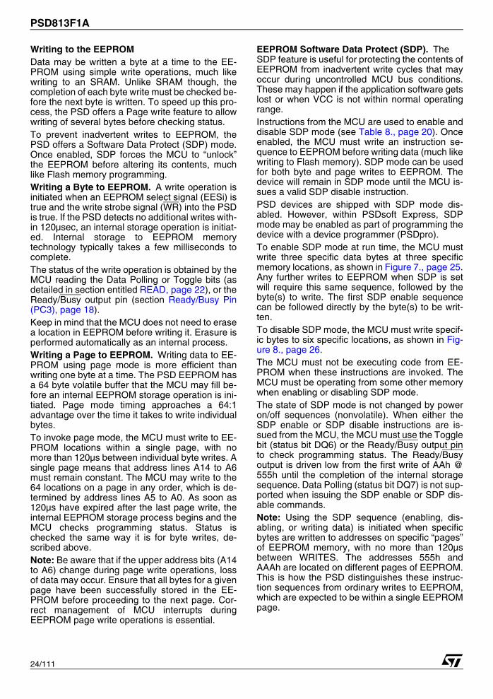
EEPROM Software Data Protect (SDP). TheSDP feature is useful for protecting the contents ofEEPROM from inadvertent write cycles that mayoccur during uncontrolled MCU bus conditions.These may happen if the application software getslost or when VCC is not within normal operatingrange.Instructions from the MCU are used to enable anddisable SDP mode (see Table 8., page 20). Onceenabled, the MCU must write an instruction se-quence to EEPROM before writing data (much likewriting to Flash memory). SDP mode can be usedfor both byte and page writes to EEPROM. Thedevice will remain in SDP mode until the MCU is-sues a valid SDP disable instruction.PSD devices are shipped with SDP mode dis-abled. However, within PSDsoft Express, SDPmode may be enabled as part of programming thedevice with a device programmer (PSDpro).To enable SDP mode at run time, the MCU mustwrite three specific data bytes at three specificmemory locations, as shown in Figure 7., page 25.Any further writes to EEPROM when SDP is setwill require this same sequence, followed by thebyte(s) to write. The first SDP enable sequencecan be followed directly by the byte(s) to be writ-ten.To disable SDP mode, the MCU must write specif-ic bytes to six specific locations, as shown in Fig-ure 8., page 26.The MCU must not be executing code from EE-PROM when these instructions are invoked. TheMCU must be operating from some other memorywhen enabling or disabling SDP mode.The state of SDP mode is not changed by poweron/off sequences (nonvolatile). When either theSDP enable or SDP disable instructions are is-sued from the MCU, the MCU must use the Togglebit (status bit DQ6) or the Ready/Busy output pinto check programming status. The Ready/Busyoutput is driven low from the first write of AAh @555h until the completion of the internal storagesequence. Data Polling (status bit DQ7) is not sup-ported when issuing the SDP enable or SDP dis-able commands.Note: Using the SDP sequence (enabling, dis-abling, or writing data) is initiated when specificbytes are written to addresses on specific “pages”of EEPROM memory, with no more than 120µsbetween WRITES. The addresses 555h andAAAh are located on different pages of EEPROM.This is how the PSD distinguishes these instruc-tion sequences from ordinary writes to EEPROM,which are expected to be within a single EEPROMpage.

25/111
PSD813F1A
Writing the OTP RowWriting to the OTP row (64 bytes) can only bedone once per byte, and is enabled by an instruc-tion. This instruction is composed of three specificWRITE operations of data bytes at three specificmemory locations followed by the data to bestored in the OTP row (refer to Table 8., page 20).
During the WRITE operations, address bit A6 mustbe zero, while address bits A5-A0 define the OTPRow byte to be written while any EEPROM SectorSelect signal (EESi) is active. Writing the OTPRow is allowed only when SDP mode is not en-abled.
Figure 7. EEPROM SDP Enable Flowcharts
WRITE AAh toAddress 555h
WRITE 55h toAddress AAAh
WRITE A0h toAddress 555h
SDP is set
Page WriteInstruction
SDP ENABLE ALGORITHM
WRITE AAh toAddress 555h
WRITE 55h toAddress AAAh
WRITE A0h toAddress 555h
Page WriteInstruction
SDPSet
SDPnot Set
WRITEis enabled
WRITE Data tobe Written inany Address
Writein Memory
Write Data+
SDP Setafter tWC
(Write Cycle Time)ai09219
PSD813F1A
26/111
Figure 8. Software Data Protection Disable Flowchart
WRITE AAh toAddress 555h
WRITE 55h toAddress AAAh
WRITE 80h toAddress 555h
Unprotected Stateafter
tWC (Write Cycle time)
Page WriteInstruction
ai09220
WRITE AAh toAddress 555h
WRITE 55h toAddress AAAh
WRITE 20h toAddress 555h
27/111
PSD813F1A
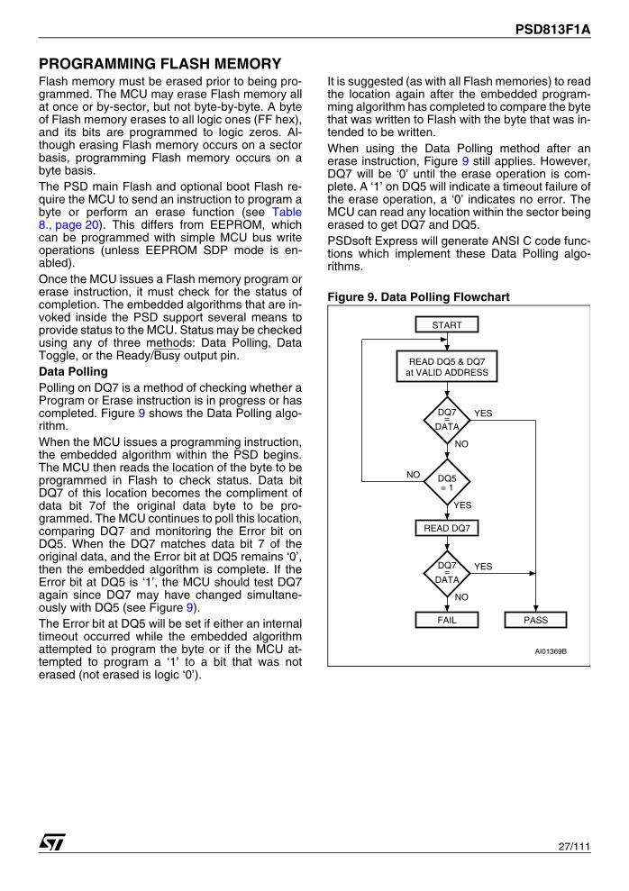
PROGRAMMING FLASH MEMORYFlash memory must be erased prior to being pro-grammed. The MCU may erase Flash memory allat once or by-sector, but not byte-by-byte. A byteof Flash memory erases to all logic ones (FF hex),and its bits are programmed to logic zeros. Al-though erasing Flash memory occurs on a sectorbasis, programming Flash memory occurs on abyte basis.The PSD main Flash and optional boot Flash re-quire the MCU to send an instruction to program abyte or perform an erase function (see Table8., page 20). This differs from EEPROM, whichcan be programmed with simple MCU bus writeoperations (unless EEPROM SDP mode is en-abled).Once the MCU issues a Flash memory program orerase instruction, it must check for the status ofcompletion. The embedded algorithms that are in-voked inside the PSD support several means toprovide status to the MCU. Status may be checkedusing any of three methods: Data Polling, DataToggle, or the Ready/Busy output pin.Data PollingPolling on DQ7 is a method of checking whether aProgram or Erase instruction is in progress or hascompleted. Figure 9 shows the Data Polling algo-rithm.When the MCU issues a programming instruction,the embedded algorithm within the PSD begins.The MCU then reads the location of the byte to beprogrammed in Flash to check status. Data bitDQ7 of this location becomes the compliment ofdata bit 7of the original data byte to be pro-grammed. The MCU continues to poll this location,comparing DQ7 and monitoring the Error bit onDQ5. When the DQ7 matches data bit 7 of theoriginal data, and the Error bit at DQ5 remains ‘0’,then the embedded algorithm is complete. If theError bit at DQ5 is ‘1’, the MCU should test DQ7again since DQ7 may have changed simultane-ously with DQ5 (see Figure 9).The Error bit at DQ5 will be set if either an internaltimeout occurred while the embedded algorithmattempted to program the byte or if the MCU at-tempted to program a ‘1’ to a bit that was noterased (not erased is logic ‘0’).
It is suggested (as with all Flash memories) to readthe location again after the embedded program-ming algorithm has completed to compare the bytethat was written to Flash with the byte that was in-tended to be written.When using the Data Polling method after anerase instruction, Figure 9 still applies. However,DQ7 will be ‘0’ until the erase operation is com-plete. A ‘1’ on DQ5 will indicate a timeout failure ofthe erase operation, a ‘0’ indicates no error. TheMCU can read any location within the sector beingerased to get DQ7 and DQ5.PSDsoft Express will generate ANSI C code func-tions which implement these Data Polling algo-rithms.
Figure 9. Data Polling Flowchart
READ DQ5 & DQ7at VALID ADDRESS
START
READ DQ7
FAIL PASS
AI01369B
DQ7=
DATA
YES
NO
YES
NO
DQ5= 1
DQ7=
DATA
YES
NO

PSD813F1A
28/111
Data ToggleChecking the Data Toggle bit on DQ6 is a methodof determining whether a Program or Erase in-struction is in progress or has completed. Figure10 shows the Data Toggle algorithm.When the MCU issues a programming instruction,the embedded algorithm within the PSD begins.The MCU then reads the location of the byte to beprogrammed in Flash to check status. Data bitDQ6 of this location will toggle each time the MCUreads this location until the embedded algorithm iscomplete. The MCU continues to read this loca-tion, checking DQ6 and monitoring the Error bit onDQ5. When DQ6 stops toggling (two consecutivereads yield the same value), and the Error bit onDQ5 remains ‘0’, then the embedded algorithm iscomplete. If the Error bit on DQ5 is ‘1’, the MCUshould test DQ6 again, since DQ6 may havechanged simultaneously with DQ5 (see Figure10).The Error bit at DQ5 will be set if either an internaltimeout occurred while the embedded algorithmattempted to program the byte, or if the MCU at-tempted to program a ‘1’ to a bit that was noterased (not erased is logic ‘0’).It is suggested (as with all Flash memories) to readthe location again after the embedded program-ming algorithm has completed to compare the bytethat was written to Flash with the byte that was in-tended to be written.When using the Data Toggle method after anerase instruction, Figure 10 still applies. DQ6 willtoggle until the erase operation is complete. A ‘1’on DQ5 will indicate a timeout failure of the eraseoperation, a ‘0’ indicates no error. The MCU canread any location within the sector being erased toget DQ6 and DQ5.
PSDsoft Express will generate ANSI C code func-tions which implement these Data Toggling algo-rithms.
Figure 10. Data Toggle Flowchart
READDQ5 & DQ6
START
READ DQ6
FAIL PASS
AI01370B
DQ6=
TOGGLENO
NO
YES
YES
DQ5= 1
NO
YES
DQ6=
TOGGLE
29/111
PSD813F1A
ERASING FLASH MEMORYFlash Bulk EraseThe Flash Bulk Erase instruction uses six write op-erations followed by a Read operation of the statusregister, as described in Table 8., page 20. If anybyte of the Bulk Erase instruction is wrong, theBulk Erase instruction aborts and the device is re-set to the Read Flash memory status.During a Bulk Erase, the memory status may bechecked by reading status bits DQ5, DQ6, andDQ7, as detailed in section entitled PROGRAM-MING FLASH MEMORY, page 27. The Error bit(DQ5) returns a ‘1’ if there has been an Erase Fail-ure (maximum number of erase cycles have beenexecuted).It is not necessary to program the array with 00hbecause the PSD will automatically do this beforeerasing to 0FFh.During execution of the Bulk Erase instruction, theFlash memory will not accept any instructions.Flash Sector Erase. The Sector Erase instruc-tion uses six write operations, as described in Ta-ble 8., page 20. Additional Flash Sector Eraseconfirm commands and Flash sector addressescan be written subsequently to erase other Flashsectors in parallel, without further coded cycles, ifthe additional instruction is transmitted in a shortertime than the timeout period of about 100 µs. Theinput of a new Sector Erase instruction will restartthe time-out period.The status of the internal timer can be monitoredthrough the level of DQ3 (Erase time-out bit). IfDQ3 is ‘0’, the Sector Erase instruction has beenreceived and the timeout is counting. If DQ3 is ‘1’,the timeout has expired and the PSD is busy eras-ing the Flash sector(s). Before and during Erasetimeout, any instruction other than Erase suspendand Erase Resume will abort the instruction andreset the device to READ mode. It is not neces-sary to program the Flash sector with 00h as thePSD will do this automatically before erasing(byte=FFh).During a Sector Erase, the memory status may bechecked by reading status bits DQ5, DQ6, andDQ7, as detailed in section entitled PROGRAM-MING FLASH MEMORY, page 27.During execution of the erase instruction, theFlash block logic accepts only Reset and Erase
Suspend instructions. Erasure of one Flash sectormay be suspended, in order to read data from an-other Flash sector, and then resumed.Flash Erase SuspendWhen a Flash Sector Erase operation is in prog-ress, the Erase Suspend instruction will suspendthe operation by writing 0B0h to any address whenan appropriate Chip Select (FSi) is true. (See Ta-ble 8., page 20). This allows reading of data fromanother Flash sector after the Erase operation hasbeen suspended. Erase suspend is accepted onlyduring the Flash Sector Erase instruction execu-tion and defaults to READ mode. An Erase Sus-pend instruction executed during an Erase timeoutwill, in addition to suspending the erase, terminatethe time out.The Toggle Bit DQ6 stops toggling when the PSDinternal logic is suspended. The toggle Bit statusmust be monitored at an address within the Flashsector being erased. The Toggle Bit will stop tog-gling between 0.1 µs and 15 µs after the EraseSuspend instruction has been executed. The PSDwill then automatically be set to Read Flash BlockMemory Array mode.If an Erase Suspend instruction was executed, thefollowing rules apply:■ Attempting to read from a Flash sector that
was being erased will output invalid data.■ Reading from a Flash sector that was not
being erased is valid.■ The Flash memory cannot be programmed,
and will only respond to Erase Resume and Reset instructions (READ is an operation and is OK).
■ If a Reset instruction is received, data in the Flash sector that was being erased will be invalid.
Flash Erase ResumeIf an Erase Suspend instruction was previously ex-ecuted, the erase operation may be resumed bythis instruction. The Erase Resume instructionconsists of writing 030h to any address while anappropriate Chip Select (FSi) is true. (See Table8., page 20.)
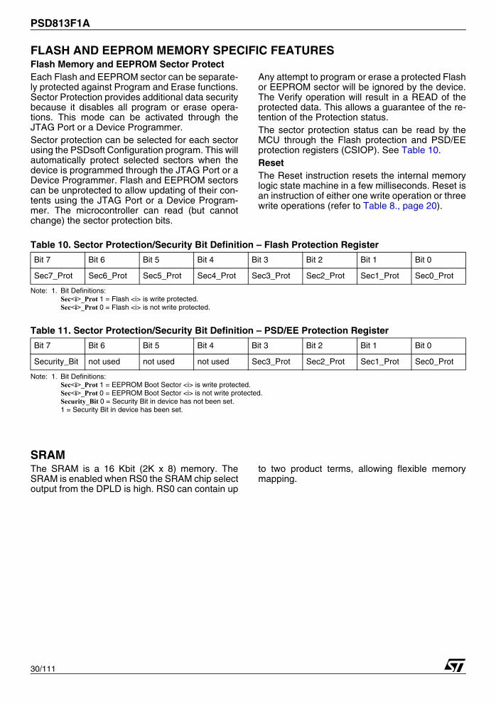
PSD813F1A
30/111
FLASH AND EEPROM MEMORY SPECIFIC FEATURESFlash Memory and EEPROM Sector ProtectEach Flash and EEPROM sector can be separate-ly protected against Program and Erase functions.Sector Protection provides additional data securitybecause it disables all program or erase opera-tions. This mode can be activated through theJTAG Port or a Device Programmer.Sector protection can be selected for each sectorusing the PSDsoft Configuration program. This willautomatically protect selected sectors when thedevice is programmed through the JTAG Port or aDevice Programmer. Flash and EEPROM sectorscan be unprotected to allow updating of their con-tents using the JTAG Port or a Device Program-mer. The microcontroller can read (but cannotchange) the sector protection bits.
Any attempt to program or erase a protected Flashor EEPROM sector will be ignored by the device.The Verify operation will result in a READ of theprotected data. This allows a guarantee of the re-tention of the Protection status.The sector protection status can be read by theMCU through the Flash protection and PSD/EEprotection registers (CSIOP). See Table 10.ResetThe Reset instruction resets the internal memorylogic state machine in a few milliseconds. Reset isan instruction of either one write operation or threewrite operations (refer to Table 8., page 20).
Table 10. Sector Protection/Security Bit Definition – Flash Protection Register
Note: 1. Bit Definitions:Sec<i>_Prot 1 = Flash <i> is write protected.Sec<i>_Prot 0 = Flash <i> is not write protected.
Table 11. Sector Protection/Security Bit Definition – PSD/EE Protection Register
Note: 1. Bit Definitions:Sec<i>_Prot 1 = EEPROM Boot Sector <i> is write protected.Sec<i>_Prot 0 = EEPROM Boot Sector <i> is not write protected.Security_Bit 0 = Security Bit in device has not been set.1 = Security Bit in device has been set.
SRAMThe SRAM is a 16 Kbit (2K x 8) memory. TheSRAM is enabled when RS0 the SRAM chip selectoutput from the DPLD is high. RS0 can contain up
to two product terms, allowing flexible memorymapping.
Bit 7 Bit 6 Bit 5 Bit 4 Bit 3 Bit 2 Bit 1 Bit 0
Sec7_Prot Sec6_Prot Sec5_Prot Sec4_Prot Sec3_Prot Sec2_Prot Sec1_Prot Sec0_Prot
Bit 7 Bit 6 Bit 5 Bit 4 Bit 3 Bit 2 Bit 1 Bit 0
Security_Bit not used not used not used Sec3_Prot Sec2_Prot Sec1_Prot Sec0_Prot

31/111
PSD813F1A
MEMORY SELECT SIGNALSThe main Flash (FSi), EEPROM (EESi), andSRAM (RS0) memory select signals are all out-puts of the DPLD. They are setup by enteringequations for them in PSDsoft Express. The fol-lowing rules apply to the equations for the internalchip select signals:1. Flash memory and EEPROM sector select
signals must not be larger than the physical sector size.
2. Any main Flash memory sector must not be mapped in the same memory space as another Flash sector.
3. An EEPROM sector must not be mapped in the same memory space as another EEPROM sector.
4. SRAM, I/O, and Peripheral I/O spaces must not overlap.
5. An EEPROM sector may overlap a main Flash memory sector. In case of overlap, priority will be given to the EEPROM.
6. SRAM, I/O, and Peripheral I/O spaces may overlap any other memory sector. Priority will be given to the SRAM, I/O, or Peripheral I/O.
ExampleFS0 is valid when the address is in the range of8000h to BFFFh, EES0 is valid from 8000h to9FFFh, and RS0 is valid from 8000h to 87FFh.Any address in the range of RS0 will always ac-cess the SRAM. Any address in the range of EES0greater than 87FFh (and less than 9FFFh) will au-tomatically address EEPROM segment 0. Any ad-dress greater than 9FFFh will access the Flashmemory segment 0. You can see that half of theFlash memory segment 0 and one-fourth of EE-PROM segment 0 can not be accessed in this ex-ample. Also note that an equation that defined FS1to anywhere in the range of 8000h to BFFFh wouldnot be valid.Figure 11 shows the priority levels for all memorycomponents. Any component on a higher level canoverlap and has priority over any component on alower level.
Components on the same level must not overlap.Level one has the highest priority and level 3 hasthe lowest.Memory Select Configuration for MCUs with Separate Program and Data SpacesThe 8031 and compatible family of microcon-trollers, which includes the 80C51, 80C151,80C251, 80C51XA, and the C500 family, haveseparate address spaces for code memory (se-lected using PSEN) and data memory (selectedusing RD). Any of the memories within the PSDcan reside in either space or both spaces. This iscontrolled through manipulation of the VM registerthat resides in the PSD’s CSIOP space.The VM register is set using PSDsoft Express tohave an initial value. It can subsequently bechanged by the microcontroller so that memorymapping can be changed on-the-fly. For example,I may wish to have SRAM and Flash in DataSpace at boot, and EEPROM in Program Space atboot, and later swap EEPROM and Flash. This iseasily done with the VM register by using PSDsoftExpress to configure it for boot up and having themicrocontroller change it when desired. Table 12describes the VM Register.
Figure 11. Priority Level of Memory and I/O Components
Table 12. VM Register
Level 1SRAM, I /O, orPeripheral I /O
Level 2Secondary
EEPROM Memory
Highest Priority
Lowest Priority
Level 3Flash Memory
AI09221
Bit 7PIO_EN Bit 6 Bit 5 Bit 4
FL_DataBit 3
EE_DataBit 2
FL_CodeBit 1
EE_CodeBit 0
SRAM_Code
0 = disablePIO mode not used not used
0 = RD can’t access Flash memory
0 = RD can’t access EEPROM
0 = PSEN can’t access Flash memory
0 = PSEN can’taccess EEPROM
0 = PSEN can’t access SRAM
1= enable PIO mode not used not used
1 = RD access Flash memory
1 = RD access EEPROM
1 = PSEN access Flash memory
1 = PSEN access EEPROM
1 = PSEN access SRAM

PSD813F1A
32/111
Separate Space ModesCode memory space is separated from data mem-ory space. For example, the PSEN signal is usedto access the program code from the Flash Mem-ory, while the RD signal is used to access datafrom the EEPROM, SRAM and I/O Ports. Thisconfiguration requires the VM register to be set to0Ch. See Figure 12.
Combined Space ModesThe program and data memory spaces are com-bined into one space that allows the main FlashMemory, EEPROM, and SRAM to be accessed byeither PSEN or RD. For example, to configure themain Flash memory in combined space mode, bits2 and 4 of the VM register are set to “1” (see Figure13).
Figure 12. 80C31 Memory Modes - Separate Space
Figure 13. 80C31 Memory Mode - Combined Space
FlashMemory
DPLD EEPROMMemory
SRAMRS0
EES0-EES3
FS0-FS7CS CSCS
OE OE
RD
PSEN
OE
AI09222
FlashMemory
DPLD EEPROMMemory
SRAMRS0
EES0-EES3
FS0-FS7
RD
CS CSCS
RD
OE OE
VM REG BIT 2
PSEN
VM REG BIT 0
VM REG BIT 1
VM REG BIT 3
VM REG BIT 4
OE
AI09223
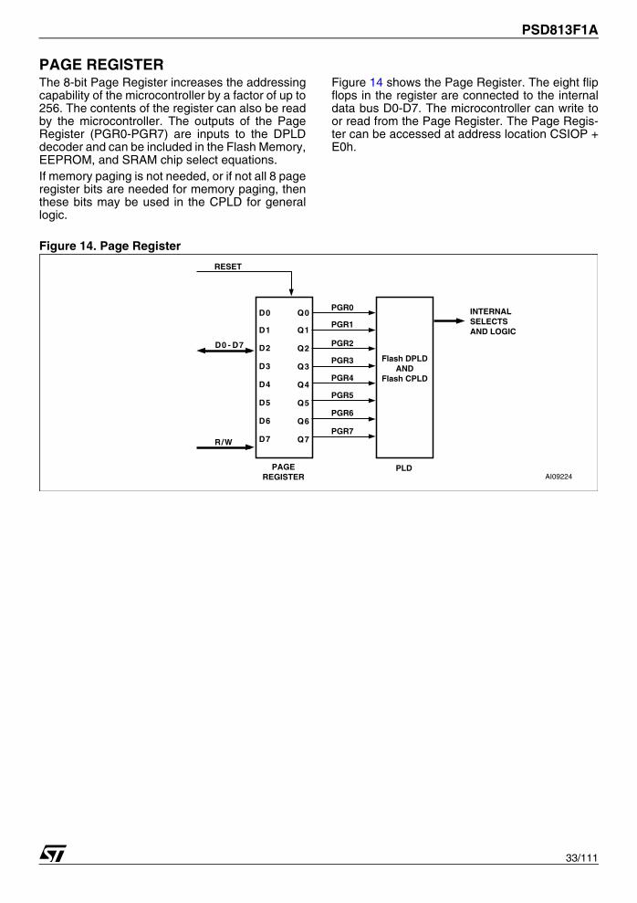
33/111
PSD813F1A
PAGE REGISTERThe 8-bit Page Register increases the addressingcapability of the microcontroller by a factor of up to256. The contents of the register can also be readby the microcontroller. The outputs of the PageRegister (PGR0-PGR7) are inputs to the DPLDdecoder and can be included in the Flash Memory,EEPROM, and SRAM chip select equations.If memory paging is not needed, or if not all 8 pageregister bits are needed for memory paging, thenthese bits may be used in the CPLD for generallogic.
Figure 14 shows the Page Register. The eight flipflops in the register are connected to the internaldata bus D0-D7. The microcontroller can write toor read from the Page Register. The Page Regis-ter can be accessed at address location CSIOP +E0h.
Figure 14. Page Register
RESET
D0 - D7
R/W
D0 Q0
Q1
Q2
Q3
Q4
Q5
Q6
Q7
D1
D2
D3
D4
D5
D6
D7
PAGEREGISTER
PGR0
PGR1
PGR2
PGR3 Flash DPLDAND
Flash CPLD
INTERNALSELECTSAND LOGIC
PLD
PGR4
PGR5
PGR6
PGR7
AI09224
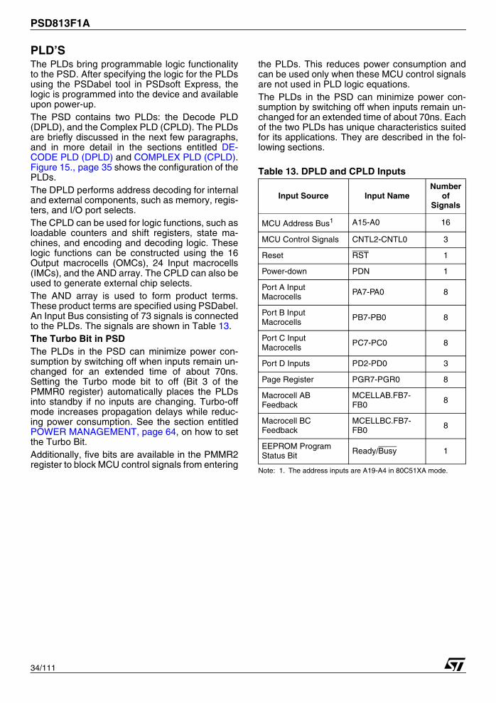
PSD813F1A
34/111
PLD’SThe PLDs bring programmable logic functionalityto the PSD. After specifying the logic for the PLDsusing the PSDabel tool in PSDsoft Express, thelogic is programmed into the device and availableupon power-up.The PSD contains two PLDs: the Decode PLD(DPLD), and the Complex PLD (CPLD). The PLDsare briefly discussed in the next few paragraphs,and in more detail in the sections entitled DE-CODE PLD (DPLD) and COMPLEX PLD (CPLD).Figure 15., page 35 shows the configuration of thePLDs.The DPLD performs address decoding for internaland external components, such as memory, regis-ters, and I/O port selects.The CPLD can be used for logic functions, such asloadable counters and shift registers, state ma-chines, and encoding and decoding logic. Theselogic functions can be constructed using the 16Output macrocells (OMCs), 24 Input macrocells(IMCs), and the AND array. The CPLD can also beused to generate external chip selects.The AND array is used to form product terms.These product terms are specified using PSDabel.An Input Bus consisting of 73 signals is connectedto the PLDs. The signals are shown in Table 13.The Turbo Bit in PSDThe PLDs in the PSD can minimize power con-sumption by switching off when inputs remain un-changed for an extended time of about 70ns.Setting the Turbo mode bit to off (Bit 3 of thePMMR0 register) automatically places the PLDsinto standby if no inputs are changing. Turbo-offmode increases propagation delays while reduc-ing power consumption. See the section entitledPOWER MANAGEMENT, page 64, on how to setthe Turbo Bit.Additionally, five bits are available in the PMMR2register to block MCU control signals from entering
the PLDs. This reduces power consumption andcan be used only when these MCU control signalsare not used in PLD logic equations.The PLDs in the PSD can minimize power con-sumption by switching off when inputs remain un-changed for an extended time of about 70ns. Eachof the two PLDs has unique characteristics suitedfor its applications. They are described in the fol-lowing sections.
Table 13. DPLD and CPLD Inputs
Note: 1. The address inputs are A19-A4 in 80C51XA mode.
Input Source Input Name Number
of Signals
MCU Address Bus1 A15-A0 16
MCU Control Signals CNTL2-CNTL0 3
Reset RST 1
Power-down PDN 1
Port A Input Macrocells PA7-PA0 8
Port B Input Macrocells PB7-PB0 8
Port C Input Macrocells PC7-PC0 8
Port D Inputs PD2-PD0 3
Page Register PGR7-PGR0 8
Macrocell AB Feedback
MCELLAB.FB7-FB0
8
Macrocell BC Feedback
MCELLBC.FB7-FB0 8
EEPROM Program Status Bit Ready/Busy 1
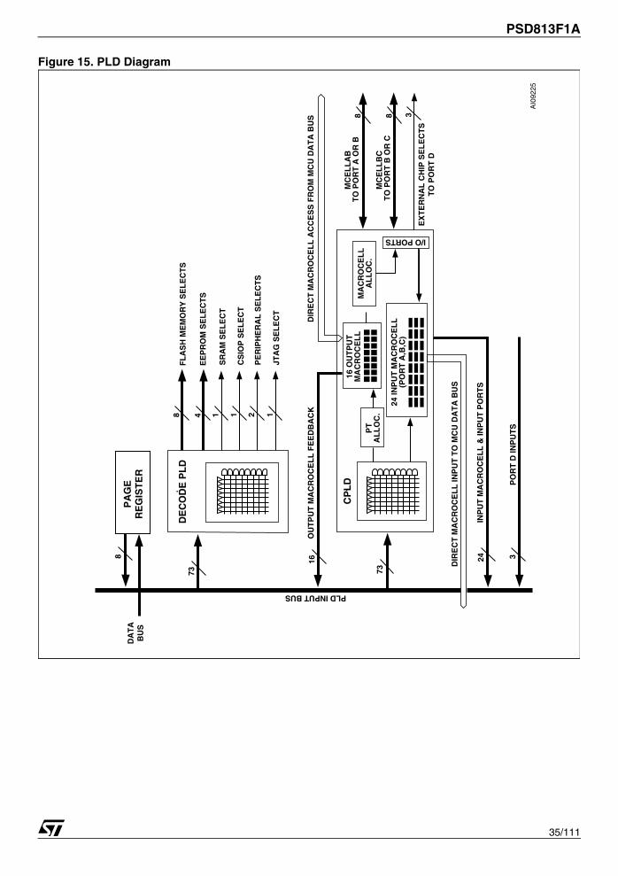
35/111
PSD813F1A
Figure 15. PLD Diagram
PLD INPUT BUS
8
INP
UT
MA
CR
OC
EL
L &
INP
UT
PO
RT
S
DIR
EC
T M
AC
RO
CE
LL
INP
UT
TO
MC
U D
AT
A B
US
CS
IOP
SE
LE
CT
SR
AM
SE
LE
CT
EE
PR
OM
SE
LE
CT
S
DE
CO
DE
PL
D
PA
GE
RE
GIS
TE
R
PE
RIP
HE
RA
L S
EL
EC
TS
JTA
G S
EL
EC
T
CP
LD
PT
AL
LO
C.
MA
CR
OC
EL
LA
LL
OC
.
MC
EL
LA
B
MC
EL
LB
C
DIR
EC
T M
AC
RO
CE
LL
AC
CE
SS
FR
OM
MC
U D
AT
A B
US
24 IN
PU
T M
AC
RO
CE
LL
(PO
RT
A,B
,C)
16 O
UT
PU
TM
AC
RO
CE
LL
I/O PORTS
FL
AS
H M
EM
OR
Y S
EL
EC
TS
3P
OR
T D
INP
UT
S
TO
PO
RT
A O
R B
TO
PO
RT
B O
R C
DA
TA
BU
S
8
8 8
4 1 1 2 1
EX
TE
RN
AL
CH
IP S
EL
EC
TS
TO
PO
RT
D
3
73
16
73
24
OU
TP
UT
MA
CR
OC
EL
L F
EE
DB
AC
K
AI0
9225
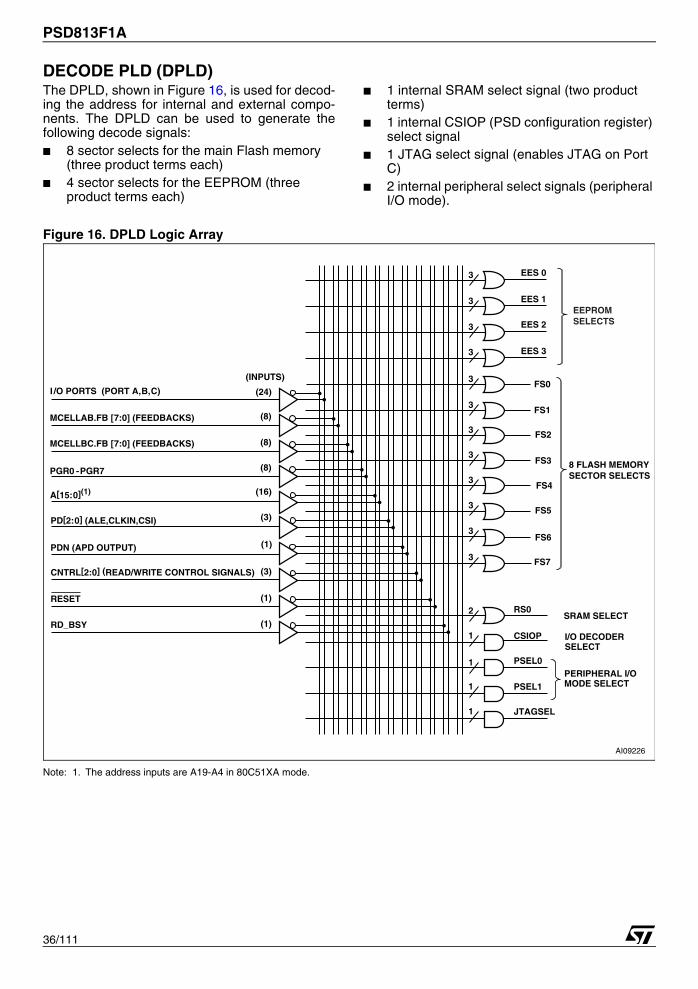
PSD813F1A
36/111
DECODE PLD (DPLD)The DPLD, shown in Figure 16, is used for decod-ing the address for internal and external compo-nents. The DPLD can be used to generate thefollowing decode signals:■ 8 sector selects for the main Flash memory
(three product terms each)■ 4 sector selects for the EEPROM (three
product terms each)
■ 1 internal SRAM select signal (two product terms)
■ 1 internal CSIOP (PSD configuration register) select signal
■ 1 JTAG select signal (enables JTAG on Port C)
■ 2 internal peripheral select signals (peripheral I/O mode).
Figure 16. DPLD Logic Array
Note: 1. The address inputs are A19-A4 in 80C51XA mode.
(INPUTS)
(24)
(8)
(16)
(1)PDN (APD OUTPUT)
I /O PORTS (PORT A,B,C)
(8)PGR0 -PGR7
(8)MCELLAB.FB [7:0] (FEEDBACKS)
MCELLBC.FB [7:0] (FEEDBACKS)
A[15:0](1)
(3)
(3)
PD[2:0] (ALE,CLKIN,CSI)
CNTRL[2:0] (READ/WRITE CONTROL SIGNALS)
(1)
(1)
RESET
RD_BSY
RS0
CSIOP
PSEL0
PSEL1
8 FLASH MEMORYSECTOR SELECTS
SRAM SELECT
I/O DECODERSELECT
PERIPHERAL I/O MODE SELECT
EES 0
EES 1
EES 2
EES 3
FS0
FS7
3
3
3
3
3
3
3
3
3
3
3
3
2
JTAGSEL
AI09226
FS1
FS2
FS3
FS6
FS5
FS4
1
1
1
1
EEPROMSELECTS
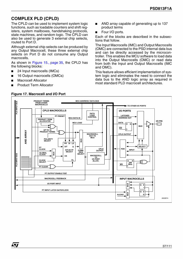
37/111
PSD813F1A
COMPLEX PLD (CPLD)The CPLD can be used to implement system logicfunctions, such as loadable counters and shift reg-isters, system mailboxes, handshaking protocols,state machines, and random logic. The CPLD canalso be used to generate 3 external chip selects,routed to Port D.Although external chip selects can be produced byany Output Macrocell, these three external chipselects on Port D do not consume any Outputmacrocells.As shown in Figure 15., page 35, the CPLD hasthe following blocks:■ 24 Input macrocells (IMCs)■ 16 Output macrocells (OMCs)■ Macrocell Allocator■ Product Term Allocator
■ AND array capable of generating up to 137 product terms
■ Four I/O ports.Each of the blocks are described in the subsec-tions that follow.The Input Macrocells (IMC) and Output Macrocells(OMC) are connected to the PSD internal data busand can be directly accessed by the microcon-troller. This enables the MCU software to load datainto the Output Macrocells (OMC) or read datafrom both the Input and Output Macrocells (IMCand OMC).This feature allows efficient implementation of sys-tem logic and eliminates the need to connect thedata bus to the AND logic array as required inmost standard PLD macrocell architectures.
Figure 17. Macrocell and I/O Port
I/O PORTSCPLD MACROCELLS
INPUT MACROCELLS
LATCHEDADDRESS OUT
MUX
MU
X
MU
X
MU
XM
UX
D
D
Q
Q
Q
G
D
Q D
WR
WR
PDR
DATA
PRODUCT TERMALLOCATOR
DIRREG.
SELECT
INPUT
PRODUCT TERMSFROM OTHERMACROCELLS
POLARITYSELECT
UP TO 10PRODUCT TERMS
CLOCKSELECT
PR DI LD
D/T
CK
CL
Q
D/T/JK FFSELECT
PT CLEAR
PT CLOCK
GLOBAL CLOCK
PT OUTPUT ENABLE (OE)
MACROCELL FEEDBACK
I/O PORT INPUT
ALE/AS
PT INPUT LATCH GATE/CLOCK
MCU LOAD
PT PRESETMCU DATA IN
COMB./REG
SELECTMACROCELL
TOI/O PORTALLOC.
CPLDOUTPUT
TO OTHER I/O PORTS
PL
D IN
PU
T B
US
PL
D IN
PU
T B
US
MCU ADDRESS / DATA BUS
MACROCELLOUT TO
MCU
DATALOAD
CONTROL
AN
D A
RR
AY
CPLD OUTPUT
I/O PIN
AI02874

PSD813F1A
38/111
Output Macrocell (OMC)Eight of the Output Macrocells (OMC) are con-nected to Ports A and B pins and are named asMcellAB0-McellAB7. The other eight macrocellsare connected to Ports B and C pins and arenamed as McellBC0-McellBC7. If an McellAB out-put is not assigned to a specific pin in PSDabel,the Macrocell Allocator will assign it to either PortA or B. The same is true for a McellBC output onPort B or C. Table 14 shows the macrocells andPort assignment.The Output Macrocell (OMC) architecture isshown in Figure 18., page 40. As shown in the fig-ure, there are native product terms available fromthe AND array, and borrowed product terms avail-able (if unused) from other OMCs. The polarity ofthe product term is controlled by the XOR gate.
The OMC can implement either sequential logic,using the flip-flop element, or combinatorial logic.The multiplexer selects between the sequential orcombinatorial logic outputs. The multiplexer outputcan drive a Port pin and has a feedback path to theAND array inputs.The flip-flop in the OMC can be configured as a D,T, JK, or SR type in the PSDabel program. Theflip-flop’s clock, preset, and clear inputs may bedriven from a product term of the AND array. Alter-natively, the external CLKIN signal can be used forthe clock input to the flip-flop. The flip-flop isclocked on the rising edge of the clock input. Thepreset and clear are active-high inputs. Each clearinput can use up to two product terms.
Table 14. Output Macrocell Port and Data Bit Assignments
OutputMacrocell
PortAssignment Native Product Terms Maximum Borrowed
Product TermsData Bit for Loading or
Reading
McellAB0 Port A0, B0 3 6 D0
McellAB1 Port A1, B1 3 6 D1
McellAB2 Port A2, B2 3 6 D2
McellAB3 Port A3, B3 3 6 D3
McellAB4 Port A4, B4 3 6 D4
McellAB5 Port A5, B5 3 6 D5
McellAB6 Port A6, B6 3 6 D6
McellAB7 Port A7, B7 3 6 D7
McellBC0 Port B0, C0 4 5 D0
McellBC1 Port B1, C1 4 5 D1
McellBC2 Port B2, C2 4 5 D2
McellBC3 Port B3, C3 4 5 D3
McellBC4 Port B4, C4 4 6 D4
McellBC5 Port B5, C5 4 6 D5
McellBC6 Port B6, C6 4 6 D6
McellBC7 Port B7, C7 4 6 D7
39/111
PSD813F1A
Product Term AllocatorThe CPLD has a Product Term Allocator. The PS-Dabel compiler uses the Product Term Allocator toborrow and place product terms from one macro-cell to another. The following list summarizes howproduct terms are allocated:■ McellAB0-McellAB7 all have three native
product terms and may borrow up to six more■ McellBC0-McellBC3 all have four native
product terms and may borrow up to five more■ McellBC4-McellBC7 all have four native
product terms and may borrow up to six more.Each macrocell may only borrow product termsfrom certain other macrocells. Product terms al-ready in use by one macrocell are not available foranother macrocell.If an equation requires more product terms thanare available to it, then “external” product termsare required, which will consume other OutputMacrocells (OMC). If external product terms areused, extra delay will be added for the equationthat required the extra product terms.This is called product term expansion. PSDsoftExpress will perform this expansion as needed.Loading and Reading the Output Macrocells(OMC). The OMCs occupy a memory location inthe MCU address space, as defined by the CSIOP(refer to the I/O section). The flip-flops in each ofthe 16 OMCs can be loaded from the data bus bya microcontroller. Loading the OMCs with datafrom the MCU takes priority over internal func-tions. As such, the preset, clear, and clock inputsto the flip-flop can be overridden by the MCU. Theability to load the flip-flops and read them back isuseful in such applications as loadable counters
and shift registers, mailboxes, and handshakingprotocols.Data can be loaded to the OMCs on the trailingedge of the WR signal (edge loading) or during thetime that the WR signal is active (level loading).The method of loading is specified in PSDsoft Ex-press Configuration.The OMC Mask RegisterThere is one Mask Register for each of the twogroups of eight OMCs. The Mask Registers can beused to block the loading of data to individualOMCs. The default value for the Mask Registers is00h, which allows loading of the OMCs. When agiven bit in a Mask Register is set to a ‘1’, the MCUwill be blocked from writing to the associatedOMC. For example, suppose McellAB0-3 are be-ing used for a state machine. You would not wanta MCU write to McellAB to overwrite the state ma-chine registers. Therefore, you would want to loadthe Mask Register for McellAB (Mask MacrocellAB) with the value 0Fh.The Output Enable of the OMCThe OMC can be connected to an I/O port pin asa PLD output. The output enable of each Port pindriver is controlled by a single product term fromthe AND array, ORed with the Direction Registeroutput. The pin is enabled upon power up if no out-put enable equation is defined and if the pin is de-clared as a PLD output in PSDsoft Express.If the OMC output is declared as an internal nodeand not as a Port pin output in the PSDabel file,then the Port pin can be used for other I/O func-tions. The internal node feedback can be routed asan input to the AND array.

PSD813F1A
40/111
Figure 18. CPLD Output Macrocell
PT
AL
LO
CA
TO
R
MA
SK
RE
G.
PT
CL
K
PT
PT
PT
CL
KIN
FE
ED
BA
CK
(.F
B)
PO
RT
INP
UT
AND ARRAY
PLD INPUT BUS
MU
X
MU
X
PO
LA
RIT
YS
EL
EC
T
LD
IN CL
R
Q
PR
DIN
CO
MB
/RE
GS
EL
EC
T
PO
RT
DR
IVE
R
INP
UT
MA
CR
OC
EL
L
I/O P
INM
AC
RO
CE
LL
AL
LO
CA
TO
R
INT
ER
NA
L D
AT
A B
US
D[ 7
:0]
DIR
EC
TIO
NR
EG
IST
ER
CL
EA
R (
.RE
)
PR
OG
RA
MM
AB
LE
FF
(D
/T/J
K/S
R)
WR
EN
AB
LE
(.O
E)
PR
ES
ET
( .P
R)
RD
MA
CR
OC
EL
L C
S
AI0
2875
B
41/111
PSD813F1A
Input Macrocells (IMC)The CPLD has 24 IMCs, one for each pin on PortsA, B, and C. The architecture of the IMC is shownin Figure 19., page 42. The IMCs are individuallyconfigurable, and can be used as a latch, register,or to pass incoming Port signals prior to drivingthem onto the PLD input bus. The outputs of theIMCs can be read by the microcontroller throughthe internal data bus.The enable for the latch and clock for the registerare driven by a multiplexer whose inputs are aproduct term from the CPLD AND array or theMCU address strobe (ALE/AS). Each product termoutput is used to latch or clock four IMCs. Port in-puts 3-0 can be controlled by one product termand 7-4 by another.Configurations for the IMCs are specified by equa-tions written in PSDabel (see Application Note 55).Outputs of the IMCs can be read by the MCU via
the IMC buffer. See the I/O Port section on how toread the IMCs.IMCs can use the address strobe to latch addressbits higher than A15. Any latched addresses arerouted to the PLDs as inputs.IMCs are particularly useful with handshakingcommunication applications where two proces-sors pass data back and forth through a commonmailbox. Figure 20., page 43 shows a typical con-figuration where the Master MCU writes to the PortA Data Out Register. This, in turn, can be read bythe Slave MCU via the activation of the “Slave-Read” output enable product term.The Slave can also write to the Port A IMCs andthe Master can then read the IMCs directly.Note that the “Slave-Read” and “Slave-wr” signalsare product terms that are derived from the SlaveMCU inputs RD, WR, and Slave_CS.
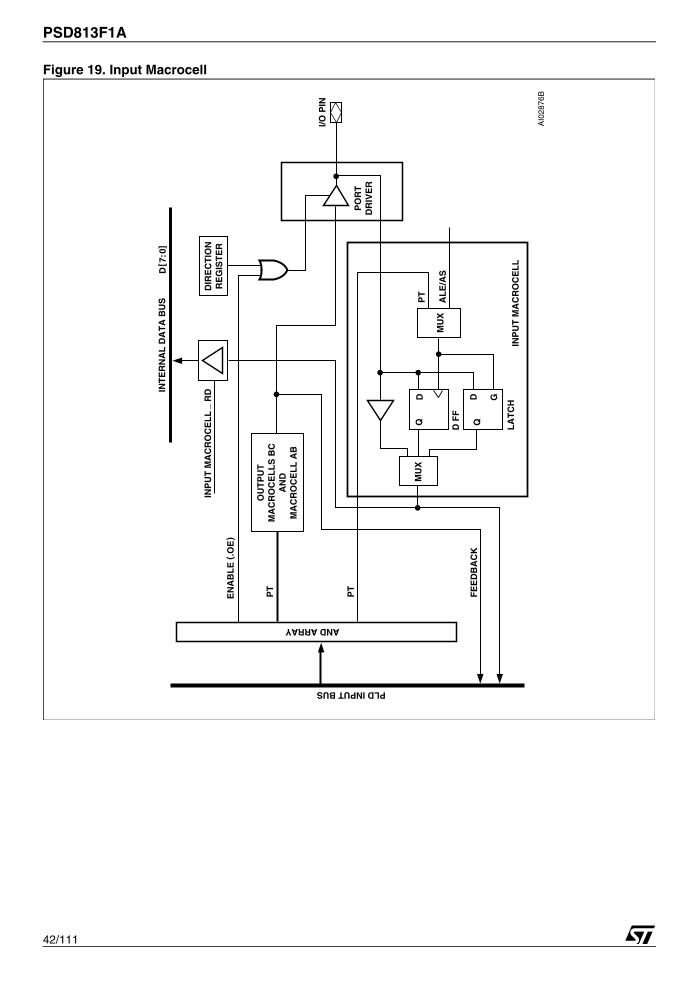
PSD813F1A
42/111
Figure 19. Input Macrocell
OU
TP
UT
MA
CR
OC
EL
LS
BC
AN
DM
AC
RO
CE
LL
AB
PT
PT
FE
ED
BA
CK
AND ARRAY
PLD INPUT BUS
PO
RT
DR
IVE
R
I/O P
IN
INT
ER
NA
L D
AT
A B
US
D[ 7
:0]
DIR
EC
TIO
NR
EG
IST
ER
MU
X
MU
X
AL
E/A
S
PT
DD G
LA
TC
HIN
PU
T M
AC
RO
CE
LL
EN
AB
LE
(.O
E)
D F
F
INP
UT
MA
CR
OC
EL
L_
RD
AI0
2876
B

43/111
PSD813F1A
Figure 20. Handshaking Communication Using Input Macrocells
MA
ST
ER
MC
U
MC
U-R
D
MC
U-R
D
MC
U-W
R
SL
AV
E–
WR
SL
AV
E–
CS
MC
U-W
R
D[ 7
:0]
D[ 7
:0]
CP
LD
DQ
QD
PO
RT
AD
AT
A O
UT
RE
GIS
TE
R
PO
RT
AIN
PU
TM
AC
RO
CE
LL
PO
RT
A
SL
AV
E–
RE
AD
SL
AV
EM
CU
RD
WR
AI0
2877
C
PS
D
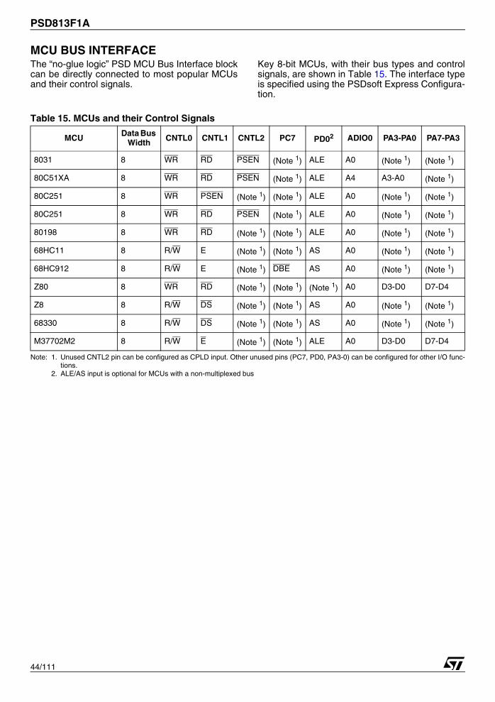
PSD813F1A
44/111
MCU BUS INTERFACEThe “no-glue logic” PSD MCU Bus Interface blockcan be directly connected to most popular MCUsand their control signals.
Key 8-bit MCUs, with their bus types and controlsignals, are shown in Table 15. The interface typeis specified using the PSDsoft Express Configura-tion.
Table 15. MCUs and their Control Signals
Note: 1. Unused CNTL2 pin can be configured as CPLD input. Other unused pins (PC7, PD0, PA3-0) can be configured for other I/O func-tions.
2. ALE/AS input is optional for MCUs with a non-multiplexed bus
MCU Data Bus Width CNTL0 CNTL1 CNTL2 PC7 PD02 ADIO0 PA3-PA0 PA7-PA3
8031 8 WR RD PSEN (Note 1) ALE A0 (Note 1) (Note 1)
80C51XA 8 WR RD PSEN (Note 1) ALE A4 A3-A0 (Note 1)
80C251 8 WR PSEN (Note 1) (Note 1) ALE A0 (Note 1) (Note 1)
80C251 8 WR RD PSEN (Note 1) ALE A0 (Note 1) (Note 1)
80198 8 WR RD (Note 1) (Note 1) ALE A0 (Note 1) (Note 1)
68HC11 8 R/W E (Note 1) (Note 1) AS A0 (Note 1) (Note 1)
68HC912 8 R/W E (Note 1) DBE AS A0 (Note 1) (Note 1)
Z80 8 WR RD (Note 1) (Note 1) (Note 1) A0 D3-D0 D7-D4
Z8 8 R/W DS (Note 1) (Note 1) AS A0 (Note 1) (Note 1)
68330 8 R/W DS (Note 1) (Note 1) AS A0 (Note 1) (Note 1)
M37702M2 8 R/W E (Note 1) (Note 1) ALE A0 D3-D0 D7-D4
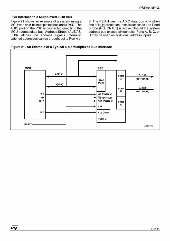
45/111
PSD813F1A
PSD Interface to a Multiplexed 8-Bit BusFigure 21 shows an example of a system using aMCU with an 8-bit multiplexed bus and a PSD. TheADIO port on the PSD is connected directly to theMCU address/data bus. Address Strobe (ALE/AS,PD0) latches the address signals internally.Latched addresses can be brought out to Port A or
B. The PSD drives the ADIO data bus only whenone of its internal resources is accessed and ReadStrobe (RD, CNTL1) is active. Should the systemaddress bus exceed sixteen bits, Ports A, B, C, orD may be used as additional address inputs.
Figure 21. An Example of a Typical 8-bit Multiplexed Bus Interface
MCU
WR
RD
BHE
ALE
RESET
AD[7:0]
A[15:8]
A[15:8]
A[7:0]
ADIOPORT
PORTA
PORTB
PORTC
WR (CNTRL0)
RD (CNTRL1)
BHE (CNTRL2)
RST
ALE (PD0)
PORT D
(OPTIONAL)
(OPTIONAL)
PSD
AI02878C
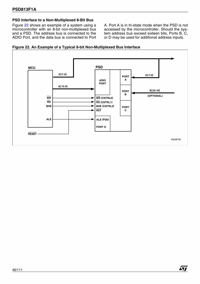
PSD813F1A
46/111
PSD Interface to a Non-Multiplexed 8-Bit BusFigure 22 shows an example of a system using amicrocontroller with an 8-bit non-multiplexed busand a PSD. The address bus is connected to theADIO Port, and the data bus is connected to Port
A. Port A is in tri-state mode when the PSD is notaccessed by the microcontroller. Should the sys-tem address bus exceed sixteen bits, Ports B, C,or D may be used for additional address inputs.
Figure 22. An Example of a Typical 8-bit Non-Multiplexed Bus Interface
MCU
WR
RD
BHE
ALE
RESET
D[7:0]
A[15:0]
A[23:16]
D[7:0]
ADIOPORT
PORTA
PORTB
PORTC
WR (CNTRL0)
RD (CNTRL1)
BHE (CNTRL2)
RST
ALE (PD0)
PORT D
(OPTIONAL)
PSD
AI02879C
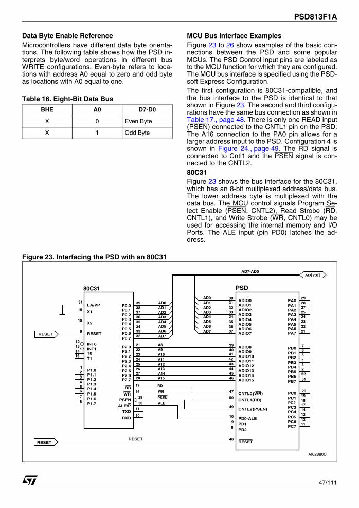
47/111
PSD813F1A
Data Byte Enable ReferenceMicrocontrollers have different data byte orienta-tions. The following table shows how the PSD in-terprets byte/word operations in different busWRITE configurations. Even-byte refers to loca-tions with address A0 equal to zero and odd byteas locations with A0 equal to one.
Table 16. Eight-Bit Data Bus
MCU Bus Interface ExamplesFigure 23 to 26 show examples of the basic con-nections between the PSD and some popularMCUs. The PSD Control input pins are labeled asto the MCU function for which they are configured.The MCU bus interface is specified using the PSD-soft Express Configuration.The first configuration is 80C31-compatible, andthe bus interface to the PSD is identical to thatshown in Figure 23. The second and third configu-rations have the same bus connection as shown inTable 17., page 48. There is only one READ input(PSEN) connected to the CNTL1 pin on the PSD.The A16 connection to the PA0 pin allows for alarger address input to the PSD. Configuration 4 isshown in Figure 24., page 49. The RD signal isconnected to Cntl1 and the PSEN signal is con-nected to the CNTL2.80C31Figure 23 shows the bus interface for the 80C31,which has an 8-bit multiplexed address/data bus.The lower address byte is multiplexed with thedata bus. The MCU control signals Program Se-lect Enable (PSEN, CNTL2), Read Strobe (RD,CNTL1), and Write Strobe (WR, CNTL0) may beused for accessing the internal memory and I/OPorts. The ALE input (pin PD0) latches the ad-dress.
Figure 23. Interfacing the PSD with an 80C31
BHE A0 D7-D0
X 0 Even Byte
X 1 Odd Byte
EA/VP
X1
X2
RESETRESET
INT0INT1T0T1
P1.0P1.1P1.2P1.3P1.4P1.5P1.6P1.7
P0.0P0.1P0.2P0.3P0.4P0.5P0.6P0.7
PA0PA1PA2PA3PA4PA5PA6PA7
PB0PB1PB2PB3PB4PB5PB6PB7
PC0
PC2PC1
PC3PC4PC5PC6PC7
P2.0P2.1P2.2P2.3P2.4P2.5P2.6P2.7
ADIO0ADIO1ADIO2ADIO3ADIO4ADIO5ADIO6ADIO7
ADIO8ADIO9ADIO10ADIO11ADIO12ADIO13ADIO14ADIO15
CNTL0(WR)
CNTL1(RD)
CNTL2(PSEN)
PD0-ALEPD1
PD2
RESET
RD
WRPSEN
ALE/P
TXD
RXD
RESET
2928272524232221
303931
19
18
9
12131415
12345678
38373635343332
AD0AD1AD2AD3AD4AD5AD6AD7
AD0AD1AD2AD3AD4AD5AD6AD7
31323334353637
3940414243444546
47
48
50
49
109
8
7654325251
PSD80C31
AD7-AD0AD[7:0]
2122232425262728
17
1629
30
A8A9A10A11A12A13A14A15
RD
WR
PSENALE
11
10
RESET
2019181714131211
AI02880C
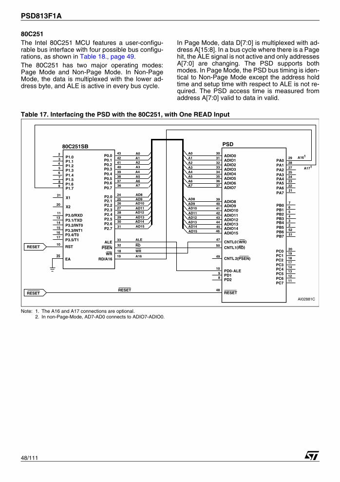
PSD813F1A
48/111
80C251The Intel 80C251 MCU features a user-configu-rable bus interface with four possible bus configu-rations, as shown in Table 18., page 49.The 80C251 has two major operating modes:Page Mode and Non-Page Mode. In Non-PageMode, the data is multiplexed with the lower ad-dress byte, and ALE is active in every bus cycle.
In Page Mode, data D[7:0] is multiplexed with ad-dress A[15:8]. In a bus cycle where there is a Pagehit, the ALE signal is not active and only addressesA[7:0] are changing. The PSD supports bothmodes. In Page Mode, the PSD bus timing is iden-tical to Non-Page Mode except the address holdtime and setup time with respect to ALE is not re-quired. The PSD access time is measured fromaddress A[7:0] valid to data in valid.
Table 17. Interfacing the PSD with the 80C251, with One READ Input
Note: 1. The A16 and A17 connections are optional.2. In non-Page-Mode, AD7-AD0 connects to ADIO7-ADIO0.
ADIO0ADIO1ADIO2ADIO3ADIO4ADIO5ADIO6ADIO7
ADIO8ADIO9ADIO10ADIO11ADIO12ADIO13ADIO14ADIO15
CNTL0 (WR)
CNTL1(RD)
CNTL 2(PSEN)
PD0-ALEPD1PD2
RESET
32
26
4342414039383736
2425
2728293031
33
A0A1A2A3A4A5A6A7
AD8AD9AD10
AD14AD15
AD13
AD11AD12
A0A1A2A3A4A5A6A7
AD8AD9AD10AD11
AD15
ALE
WR
A16
RD
AD14
AD12AD13
14
9
2345678
21
20
1113
P1.0P1.1P1.2P1.3P1.4P1.5P1.6P1.7
P3.0/RXDP3.1/TXDP3.2/INT0
X2
X1
P3.3/INT1
RST
EA
A161P0.1P0.0
P0.2P0.3P0.4P0.5P0.6P0.7
P2.0P2.1P2.2P2.3P2.4P2.5P2.6P2.7
ALEPSEN
WRRD/A16
PC0PC1
PC3PC4PC5PC6PC7
19
18
3031323334353637
3940414243444546
48
89
10
49
50
47
2928272524232221
2019181714131211
PB0PB1PB2PB3PB4PB5PB6PB7
PA0PA1PA2PA3PA4PA5PA6PA7
7654325251
80C251SB PSD
RESET
RESET
35
P3.4/T0P3.5/T1
1615
17
10
RESET
PC2
AI02881C
A171
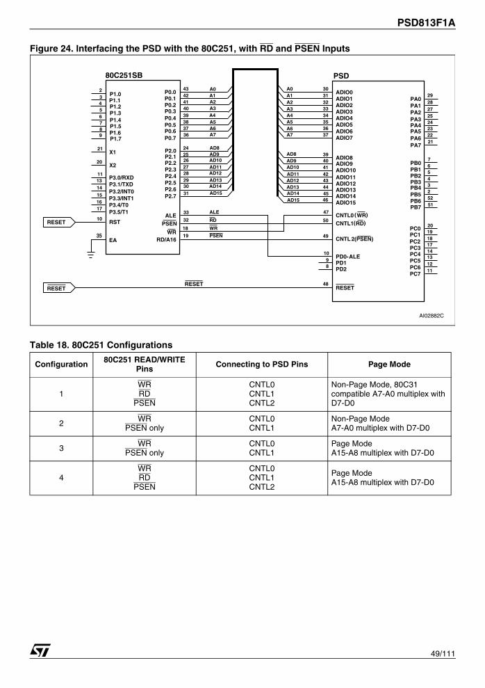
49/111
PSD813F1A
Figure 24. Interfacing the PSD with the 80C251, with RD and PSEN Inputs
Table 18. 80C251 Configurations
Configuration 80C251 READ/WRITE Pins Connecting to PSD Pins Page Mode
1 WRRD
PSEN
CNTL0 CNTL1 CNTL2
Non-Page Mode, 80C31 compatible A7-A0 multiplex with D7-D0
2 WRPSEN only
CNTL0 CNTL1
Non-Page ModeA7-A0 multiplex with D7-D0
3 WRPSEN only
CNTL0 CNTL1
Page ModeA15-A8 multiplex with D7-D0
4 WRRD
PSEN
CNTL0 CNTL1 CNTL2
Page ModeA15-A8 multiplex with D7-D0
ADIO0ADIO1ADIO2ADIO3ADIO4ADIO5ADIO6ADIO7
ADIO8ADIO9ADIO10ADIO11ADIO12ADIO13ADIO14ADIO15
CNTL0 (WR)
CNTL1(RD)
CNTL 2(PSEN)
PD0-ALEPD1PD2
RESET
32
26
4342414039383736
2425
2728293031
33
A0A1A2A3A4A5A6A7
AD8AD9AD10
AD14AD15
AD13
AD11AD12
A0A1A2A3A4A5A6A7
AD8AD9AD10AD11
AD15
ALE
WR
PSEN
RD
AD14
AD12AD13
14
9
2345678
21
20
1113
P1.0P1.1P1.2P1.3P1.4P1.5P1.6P1.7
P3.0/RXDP3.1/TXDP3.2/INT0
X2
X1
P3.3/INT1
RST
EA
P0.1P0.0
P0.2P0.3P0.4P0.5P0.6P0.7
P2.0P2.1P2.2P2.3P2.4P2.5P2.6P2.7
ALEPSEN
WRRD/A16
PC0PC1
PC3PC4PC5PC6PC7
19
18
3031323334353637
3940414243444546
48
89
10
49
50
47
2928272524232221
2019181714131211
PB0PB1PB2PB3PB4PB5PB6PB7
PA0PA1PA2PA3PA4PA5PA6PA7
7654325251
80C251SB PSD
RESET
RESET
35
P3.4/T0P3.5/T1
1615
17
10
RESET
PC2
AI02882C
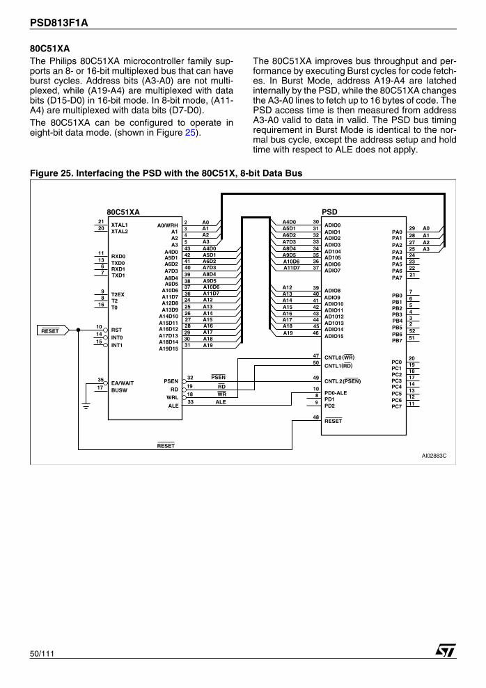
PSD813F1A
50/111
80C51XAThe Philips 80C51XA microcontroller family sup-ports an 8- or 16-bit multiplexed bus that can haveburst cycles. Address bits (A3-A0) are not multi-plexed, while (A19-A4) are multiplexed with databits (D15-D0) in 16-bit mode. In 8-bit mode, (A11-A4) are multiplexed with data bits (D7-D0).The 80C51XA can be configured to operate ineight-bit data mode. (shown in Figure 25).
The 80C51XA improves bus throughput and per-formance by executing Burst cycles for code fetch-es. In Burst Mode, address A19-A4 are latchedinternally by the PSD, while the 80C51XA changesthe A3-A0 lines to fetch up to 16 bytes of code. ThePSD access time is then measured from addressA3-A0 valid to data in valid. The PSD bus timingrequirement in Burst Mode is identical to the nor-mal bus cycle, except the address setup and holdtime with respect to ALE does not apply.
Figure 25. Interfacing the PSD with the 80C51X, 8-bit Data Bus
ADIO0ADIO1ADIO2ADIO3AD104AD105ADIO6ADIO7
ADIO8ADIO9ADIO10ADIO11AD1012AD1013ADIO14ADIO15
CNTL0 (WR)
CNTL1(RD)
CNTL 2(PSEN)
PD0-ALEPD1PD2
RESET
31
33
36
234543424140393837
24252627282930
A4D0A5D1A6D2A7D3A8D4A9D5A10D6A11D7
A12A13A14
A18A19
A17
A15A16
A0A1A2A3A4D0A5D1A6D2A7D3A8D4A9D5A10D6A11D7A12
A16A17A18A19
A15
A13A14
TXD1
T2EXT2T0
RST
EA/WAITBUSW
A1A0/WRH
A2A3
A4D0A5D1A6D2A7D3A8D4A9D5
A10D6A11D7A12D8A13D9
A14D10A15D11A16D12A17D13A18D14A19D15
PSEN
RD
WRL
PC0PC1
PC3PC4PC5PC6PC7ALE
PSEN
RDWR
ALE
32
19
18
3031323334353637
3940414243444546
48
89
10
49
5047
7
98
16
XTAL1XTAL2
RXD0TXD0RXD1
2120
11136
2928272524232221
2019181714131211
PB0PB1PB2PB3PB4PB5PB6PB7
PA0PA1PA2PA3PA4PA5PA6PA7
7654325251
A0A1A2A3
80C51XA PSD
RESET
RESET
35
17
INT0INT1
1410
15
PC2
AI02883C

51/111
PSD813F1A
68HC11Figure 26 shows an interface to a 68HC11 wherethe PSD is configured in 8-bit multiplexed mode
with E and R/W settings. The DPLD can generatethe READ and WR signals for external devices.
Figure 26. Interfacing the PSD with a 68HC11
910111213141516
ADIO0ADIO1ADIO2ADIO3AD104AD105ADIO6ADIO7
ADIO8ADIO9ADIO10ADIO11AD1012AD1013ADIO14ADIO15
CNTL0 (R_W)CNTL1(E)
CNTL 2
PD0–ASPD1PD2
RESET
202122232425
3
5
4
6
4241403938373635
AD0
AD0AD1AD2AD3AD4AD5AD6AD7
A8A9A10
A14A15
A13
A11A12
AD1AD2AD3AD4AD5AD6AD7
E
AS
R/W
XT
EX
RESETIRQXIRQ
PA0PA1PA2
PE0PE1PE2PE3PE4PE5PE6PE7
VRHVRL
PA3PA4PA5PA6PA7
PB0PB1PB2PB3PB4PB5PB6PB7
PA0PA1PA2PA3PA4PA5PA6PA7
PC0PC1PC2PC3PC4PC5PC6PC7
PC0PC1
PC3PC4PC5PC6PC7
PD0PD1PD2PD3PD4PD5
MODA
EAS
R/W
31
3031323334353637
3940414243444546
48
89
10
49
5047
8
7
171918
343332
4344454647484950
5251
30292827
2928272524232221
2019181714131211
PB0PB1PB2PB3PB4PB5PB6PB7
7654325251
MODB2
68HC11
PSD
RESET
RESET
AD7-AD0AD7-AD0
PC2
AI02884C
PSD813F1A
52/111
I/O PORTSThere are four programmable I/O ports: Ports A, B,C, and D. Each of the ports is eight bits except PortD, which is 3 bits. Each port pin is individually userconfigurable, thus allowing multiple functions perport. The ports are configured using PSDsoft Ex-press Configuration or by the MCU writing to on-chip registers in the CSIOP address space.The topics discussed in this section are:■ General Port architecture■ Port Operating Modes■ Port Configuration Registers (PCR)■ Port Data Registers■ Individual Port Functionality.General Port ArchitectureThe general architecture of the I/O Port is shownin Figure 27., page 53. Individual Port architec-tures are shown in Figure 29., page 60 to Figure32., page 63. In general, once the purpose for aport pin has been defined, that pin will no longer beavailable for other purposes. Exceptions will benoted.As shown in Figure 27., page 53, the ports containan output multiplexer whose selects are driven bythe configuration bits in the Control Registers(Ports A and B only) and PSDsoft Express Config-uration. Inputs to the multiplexer include the fol-lowing:■ Output data from the Data Out Register■ Latched address outputs■ CPLD Macrocell output■ External Chip Select from CPLD.The Port Data Buffer (PDB) is a tri-state buffer thatallows only one source at a time to be read. ThePDB is connected to the Internal Data Bus forfeedback and can be read by the microcontroller.The Data Out and Macrocell outputs, Directionand Control Registers, and port pin input are allconnected to the PDB.
The Port pin’s tri-state output driver enable is con-trolled by a two input OR gate whose inputs comefrom the CPLD AND array enable product termand the Direction Register. If the enable productterm of any of the array outputs are not definedand that port pin is not defined as a CPLD outputin the PSDabel file, then the Direction Register hassole control of the buffer that drives the port pin.The contents of these registers can be altered bythe microcontroller. The PDB feedback path al-lows the microcontroller to check the contents ofthe registers.Ports A, B, and C have embedded Input Macro-cells (IMCs). The IMCs can be configured as latch-es, registers, or direct inputs to the PLDs. Thelatches and registers are clocked by the addressstrobe (AS/ALE) or a product term from the PLDAND array. The outputs from the IMCs drive thePLD input bus and can be read by the microcon-troller. See the section entitled InputMacrocell, page 42.Port Operating ModesThe I/O Ports have several modes of operation.Some modes can be defined using PSDabel,some by the microcontroller writing to the ControlRegisters in CSIOP space, and some by both. Themodes that can only be defined using PSDsoft Ex-press must be programmed into the device andcannot be changed unless the device is repro-grammed. The modes that can be changed by themicrocontroller can be done so dynamically at run-time. The PLD I/O, Data Port, Address Input, andPeripheral I/O modes are the only modes thatmust be defined before programming the device.All other modes can be changed by the microcon-troller at run-time.Table 19., page 54 summarizes which modes areavailable on each port. Table 22., page 57 showshow and where the different modes are config-ured. Each of the port operating modes are de-scribed in the following subsections.

53/111
PSD813F1A
Figure 27. General I/O Port ArchitectureIN
TE
RN
AL
DA
TA
BU
S
DATA OUTREG.
D Q
D
G
Q
D Q
D Q
WR
WR
WR
ADDRESS
MACROCELL OUTPUTS
ENABLE PRODUCT TERM (.OE)
EXT CS
ALE
READ MUX
P
D
B
CPLD-INPUT
CONTROL REG.
DIR REG.
INPUTMACROCELL
ENABLE OUT
DATA IN
OUTPUTSELECT
OUTPUTMUX
PORT PIN
DATA OUT
ADDRESS
AI02885
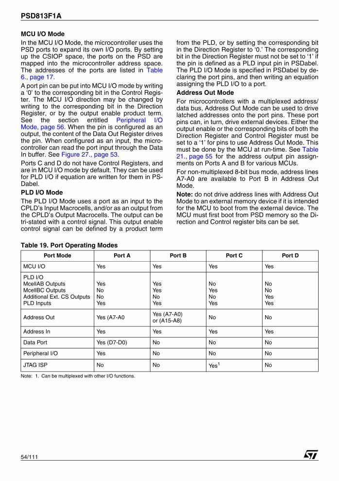
PSD813F1A
54/111
MCU I/O ModeIn the MCU I/O Mode, the microcontroller uses thePSD ports to expand its own I/O ports. By settingup the CSIOP space, the ports on the PSD aremapped into the microcontroller address space.The addresses of the ports are listed in Table6., page 17.A port pin can be put into MCU I/O mode by writinga ‘0’ to the corresponding bit in the Control Regis-ter. The MCU I/O direction may be changed bywriting to the corresponding bit in the DirectionRegister, or by the output enable product term.See the section entitled Peripheral I/OMode, page 56. When the pin is configured as anoutput, the content of the Data Out Register drivesthe pin. When configured as an input, the micro-controller can read the port input through the DataIn buffer. See Figure 27., page 53.Ports C and D do not have Control Registers, andare in MCU I/O mode by default. They can be usedfor PLD I/O if equation are written for them in PS-Dabel.PLD I/O ModeThe PLD I/O Mode uses a port as an input to theCPLD’s Input Macrocells, and/or as an output fromthe CPLD’s Output Macrocells. The output can betri-stated with a control signal. This output enablecontrol signal can be defined by a product term
from the PLD, or by setting the corresponding bitin the Direction Register to ‘0.’ The correspondingbit in the Direction Register must not be set to ‘1’ ifthe pin is defined as a PLD input pin in PSDabel.The PLD I/O Mode is specified in PSDabel by de-claring the port pins, and then writing an equationassigning the PLD I/O to a port.Address Out ModeFor microcontrollers with a multiplexed address/data bus, Address Out Mode can be used to drivelatched addresses onto the port pins. These portpins can, in turn, drive external devices. Either theoutput enable or the corresponding bits of both theDirection Register and Control Register must beset to a ‘1’ for pins to use Address Out Mode. Thismust be done by the MCU at run-time. See Table21., page 55 for the address output pin assign-ments on Ports A and B for various MCUs.For non-multiplexed 8-bit bus mode, address linesA7-A0 are available to Port B in Address OutMode.Note: do not drive address lines with Address OutMode to an external memory device if it is intendedfor the MCU to boot from the external device. TheMCU must first boot from PSD memory so the Di-rection and Control register bits can be set.
Table 19. Port Operating Modes
Note: 1. Can be multiplexed with other I/O functions.
Port Mode Port A Port B Port C Port D
MCU I/O Yes Yes Yes Yes
PLD I/OMcellAB Outputs McellBC Outputs Additional Ext. CS Outputs PLD Inputs
Yes No No Yes
Yes Yes No Yes
No Yes No Yes
NoNoYesYes
Address Out Yes (A7-A0 Yes (A7-A0)or (A15-A8) No No
Address In Yes Yes Yes Yes
Data Port Yes (D7-D0) No No No
Peripheral I/O Yes No No No
JTAG ISP No No Yes1 No

55/111
PSD813F1A
Table 20. Port Operating Mode Settings
Note: 1. N/A = Not Applicable2. The direction of the Port A,B,C, and D pins are controlled by the Direction Register ORed with the individual output enable product
term (.oe) from the CPLD AND Array.3. Any of these three methods enables the JTAG pins on Port C.
Table 21. I/O Port Latched Address Output Assignments
Note: 1. N/A = Not Applicable.
Mode Defined in PSDabel
Defined in PSD Configuration
Control Register Setting
Direction Register Setting
VM Register Setting
JTAG Enable
MCU I/O Declare pins only N/A1 01 = output,0 = input(Note 2)
N/A N/A
PLD I/O Logic equations N/A N/A (Note 2) N/A N/A
Data Port (Port A) N/A Specify bus type N/A N/A N/A N/A
Address Out (Port A,B) Declare pins only N/A 1 1 (Note 2) N/A N/A
Address In(Port A,B,C,D)
Logic equation for Input Macrocells
N/A N/A N/A N/A N/A
Peripheral I/O(Port A)
Logic equations(PSEL0 & 1)
N/A N/A N/A PIO bit = 1 N/A
JTAG ISP (Note 3) JTAGSEL JTAG Configuration N/A N/A N/A JTAG_Enable
MCU Port A (PA3-PA0) Port A (PA7-PA4) Port B (PB3-PB0) Port B (PB7-PB4)
8051XA (8-Bit) N/A1 Address a7-a4 Address A11-A8 N/A
80C251 (Page Mode) N/A N/A Address A11-A8 Address A15-A12
All Other 8-Bit Multiplexed Address A3-A0 Address A7-A4 Address A3-A0 Address A7-A4
8-Bit Non-Multiplexed Bus
N/A N/A Address A3-A0 Address A7-A4
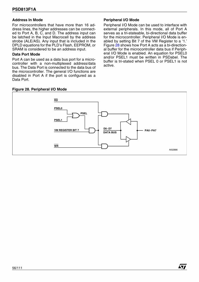
PSD813F1A
56/111
Address In ModeFor microcontrollers that have more than 16 ad-dress lines, the higher addresses can be connect-ed to Port A, B, C, and D. The address input canbe latched in the Input Macrocell by the addressstrobe (ALE/AS). Any input that is included in theDPLD equations for the PLD’s Flash, EEPROM, orSRAM is considered to be an address input.Data Port ModePort A can be used as a data bus port for a micro-controller with a non-multiplexed address/databus. The Data Port is connected to the data bus ofthe microcontroller. The general I/O functions aredisabled in Port A if the port is configured as aData Port.
Peripheral I/O ModePeripheral I/O Mode can be used to interface withexternal peripherals. In this mode, all of Port Aserves as a tri-stateable, bi-directional data bufferfor the microcontroller. Peripheral I/O Mode is en-abled by setting Bit 7 of the VM Register to a ‘1.’Figure 28 shows how Port A acts as a bi-direction-al buffer for the microcontroller data bus if Periph-eral I/O Mode is enabled. An equation for PSEL0and/or PSEL1 must be written in PSDabel. Thebuffer is tri-stated when PSEL 0 or PSEL1 is notactive.
Figure 28. Peripheral I/O Mode
RD
PSEL0
PSEL1
PSEL
VM REGISTER BIT 7
WR
PA0 - PA7D0 - D7
DATA BUS
AI02886

57/111
PSD813F1A
JTAG In-System Programming (ISP)Port C is JTAG compliant, and can be used for In-System Programming (ISP). You can multiplexJTAG operations with other functions on Port Cbecause ISP is not performed during normal sys-tem operation. For more information on the JTAGPort, see the section entitled PROGRAMMING IN-CIRCUIT USING THE JTAG SERIALINTERFACE, page 71.Port Configuration Registers (PCR)Each Port has a set of Port Configuration Regis-ters (PCR) used for configuration. The contents ofthe registers can be accessed by the MCU throughnormal READ/WRITE bus cycles at the addressesgiven in Table 6., page 17. The addresses in Ta-ble 6., page 17 are the offsets in hexadecimal fromthe base of the CSIOP register.
The pins of a port are individually configurable andeach bit in the register controls its respective pin.For example, Bit 0 in a register refers to Bit 0 of itsport. The three Port Configuration Registers(PCR), shown in Table 22, are used for setting thePort configurations. The default Power-up state foreach register in Table 22 is 00h.Control RegisterAny bit reset to ‘0’ in the Control Register sets thecorresponding port pin to MCU I/O Mode, and a ‘1’sets it to Address Out Mode. The default mode isMCU I/O. Only Ports A and B have an associatedControl Register.
Table 22. Port Configuration Registers (PCR)
Note: 1. See Table 26., page 58 for Drive Register bit definition.
Register Name Port MCU Access
Control A,B WRITE/READ
Direction A,B,C,D WRITE/READ
Drive Select1 A,B,C,D WRITE/READ
PSD813F1A
58/111
Direction RegisterThe Direction Register, in conjunction with the out-put enable (except for Port D), controls the direc-tion of data flow in the I/O Ports. Any bit set to ‘1’in the Direction Register will cause the corre-sponding pin to be an output, and any bit set to ‘0’will cause it to be an input. The default mode for allport pins is input.Figure 29., page 60 and Figure 30., page 61 showthe Port Architecture diagrams for Ports A/B andC, respectively. The direction of data flow for PortsA, B, and C are controlled not only by the directionregister, but also by the output enable productterm from the PLD AND array. If the output enableproduct term is not active, the Direction Registerhas sole control of a given pin’s direction.An example of a configuration for a port with thethree least significant bits set to output and the re-mainder set to input is shown in Table 25. SincePort D only contains three pins (shown in Figure32., page 63), the Direction Register for Port Dhas only the three least significant bits active.Drive Select RegisterThe Drive Select Register configures the pin driveras Open Drain or CMOS for some port pins, andcontrols the slew rate for the other port pins. Anexternal pull-up resistor should be used for pinsconfigured as Open Drain.A pin can be configured as Open Drain if its corre-sponding bit in the Drive Select Register is set to a‘1.’ The default pin drive is CMOS.Aside: the slew rate is a measurement of the riseand fall times of an output. A higher slew ratemeans a faster output response and may create
more electrical noise. A pin operates in a high slewrate when the corresponding bit in the Drive Reg-ister is set to ‘1.’ The default rate is slow slew.Table 26 shows the Drive Register for Ports A, B,C, and D. It summarizes which pins can be config-ured as Open Drain outputs and which pins theslew rate can be set for.
Table 23. Port Pin Direction Control, Output Enable P.T. Not Defined
Table 24. Port Pin Direction Control, Output Enable P.T. Defined
Table 25. Port Direction Assignment Example
Table 26. Drive Register Pin Assignment
Note: 1. NA = Not Applicable.
Direction Register Bit Port Pin Mode
0 Input
1 Output
Direction Register Bit
Output Enable P.T. Port Pin Mode
0 0 Input
0 1 Output
1 0 Output
1 1 Output
Bit 7 Bit 6 Bit 5 Bit 4 Bit 3 Bit 2 Bit 1 Bit 0
0 0 0 0 0 1 1 1
Drive Register Bit 7 Bit 6 Bit 5 Bit 4 Bit 3 Bit 2 Bit 1 Bit 0
Port A OpenDrain
OpenDrain
OpenDrain
OpenDrain
SlewRate
SlewRate
SlewRate
SlewRate
Port B OpenDrain
OpenDrain
OpenDrain
OpenDrain
SlewRate
SlewRate
SlewRate
SlewRate
Port C OpenDrain
OpenDrain
OpenDrain
OpenDrain
OpenDrain
OpenDrain
OpenDrain
OpenDrain
Port D NA1 NA1 NA1 NA1 NA1 SlewRate
SlewRate
SlewRate
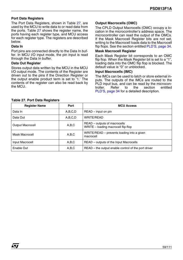
59/111
PSD813F1A
Port Data RegistersThe Port Data Registers, shown in Table 27, areused by the MCU to write data to or read data fromthe ports. Table 27 shows the register name, theports having each register type, and MCU accessfor each register type. The registers are describedbelow.Data InPort pins are connected directly to the Data In buf-fer. In MCU I/O input mode, the pin input is readthrough the Data In buffer.Data Out RegisterStores output data written by the MCU in the MCUI/O output mode. The contents of the Register aredriven out to the pins if the Direction Register orthe output enable product term is set to ‘1.’ Thecontents of the register can also be read back bythe MCU.
Output Macrocells (OMC)The CPLD Output Macrocells (OMC) occupy a lo-cation in the microcontroller’s address space. Themicrocontroller can read the output of the OMCs.If the Mask Macrocell Register bits are not set,writing to the Macrocell loads data to the Macrocellflip flops. See the section entitled PLD’S, page 34.Mask Macrocell RegisterEach Mask Register bit corresponds to an OMCflip flop. When the Mask Register bit is set to a “1”,loading data into the OMC flip flop is blocked. Thedefault value is “0” or unblocked.Input Macrocells (IMC)The IMCs can be used to latch or store external in-puts. The outputs of the IMCs are routed to thePLD input bus, and can be read by the microcon-troller. Refer to the section entitledPLD’S, page 34 for a detailed description.
Table 27. Port Data Registers
Register Name Port MCU Access
Data In A,B,C,D READ – input on pin
Data Out A,B,C,D WRITE/READ
Output Macrocell A,B,C READ – outputs of macrocellsWRITE – loading macrocell flip-flop
Mask Macrocell A,B,C WRITE/READ – prevents loading into a givenmacrocell
Input Macrocell A,B,C READ – outputs of the Input Macrocells
Enable Out A,B,C READ – the output enable control of the port driver
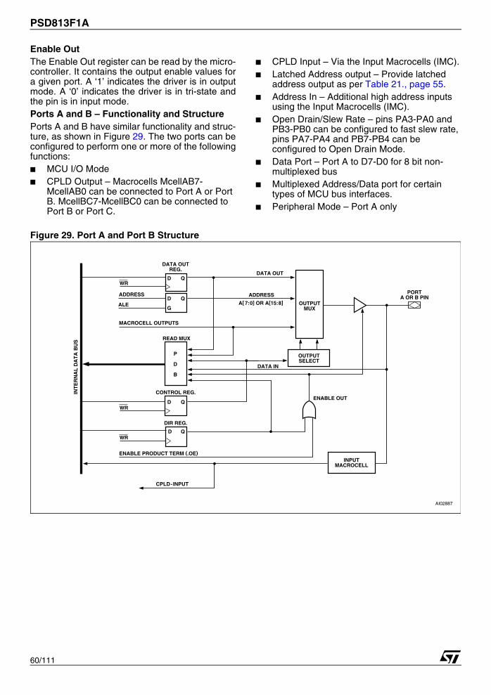
PSD813F1A
60/111
Enable OutThe Enable Out register can be read by the micro-controller. It contains the output enable values fora given port. A ‘1’ indicates the driver is in outputmode. A ‘0’ indicates the driver is in tri-state andthe pin is in input mode.Ports A and B – Functionality and StructurePorts A and B have similar functionality and struc-ture, as shown in Figure 29. The two ports can beconfigured to perform one or more of the followingfunctions:■ MCU I/O Mode■ CPLD Output – Macrocells McellAB7-
McellAB0 can be connected to Port A or Port B. McellBC7-McellBC0 can be connected to Port B or Port C.
■ CPLD Input – Via the Input Macrocells (IMC).■ Latched Address output – Provide latched
address output as per Table 21., page 55.■ Address In – Additional high address inputs
using the Input Macrocells (IMC).■ Open Drain/Slew Rate – pins PA3-PA0 and
PB3-PB0 can be configured to fast slew rate, pins PA7-PA4 and PB7-PB4 can be configured to Open Drain Mode.
■ Data Port – Port A to D7-D0 for 8 bit non-multiplexed bus
■ Multiplexed Address/Data port for certain types of MCU bus interfaces.
■ Peripheral Mode – Port A only
Figure 29. Port A and Port B Structure
INT
ER
NA
L D
AT
A B
US
DATA OUTREG.
D Q
D
G
Q
D Q
D Q
WR
WR
WR
ADDRESS
MACROCELL OUTPUTS
ENABLE PRODUCT TERM (.OE)
ALE
READ MUX
P
D
B
CPLD-INPUT
CONTROL REG.
DIR REG.
INPUTMACROCELL
ENABLE OUT
DATA IN
OUTPUTSELECT
OUTPUTMUX
PORTA OR B PIN
DATA OUT
ADDRESS
A[ 7:0] OR A[15:8]
AI02887

61/111
PSD813F1A
Port C – Functionality and StructurePort C can be configured to perform one or moreof the following functions (see Figure 30):■ MCU I/O Mode■ CPLD Output – McellBC7-McellBC0 outputs
can be connected to Port B or Port C.■ CPLD Input – via the Input Macrocells (IMC)■ Address In – Additional high address inputs
using the Input Macrocells (IMC).■ In-System Programming (ISP) – JTAG port
can be enabled for programming/erase of the
PSD device. (See the section entitled PROGRAMMING IN-CIRCUIT USING THE JTAG SERIAL INTERFACE, page 71, for more information on JTAG programming.)
■ Open Drain – Port C pins can be configured in Open Drain Mode
Port C does not support Address Out mode, andtherefore no Control Register is required.Pin PC7 may be configured as the DBE input incertain MCU interfaces.
Figure 30. Port C Structure
Note: 1. ISP.
INT
ER
NA
L D
AT
A B
US
DATA OUTREG.
D Q
D Q
WR
WR
MCELLBC[ 7:0]
ENABLE PRODUCT TERM (.OE)
READ MUX
P
D
B
CPLD-INPUT
DIR REG.
INPUTMACROCELL
ENABLE OUT
SPECIAL FUNCTION1
SPECIAL FUNCTION1
CONFIGURATIONBIT
DATA IN
OUTPUTSELECT
OUTPUTMUX
PORT C PIN
DATA OUT
AI02888B
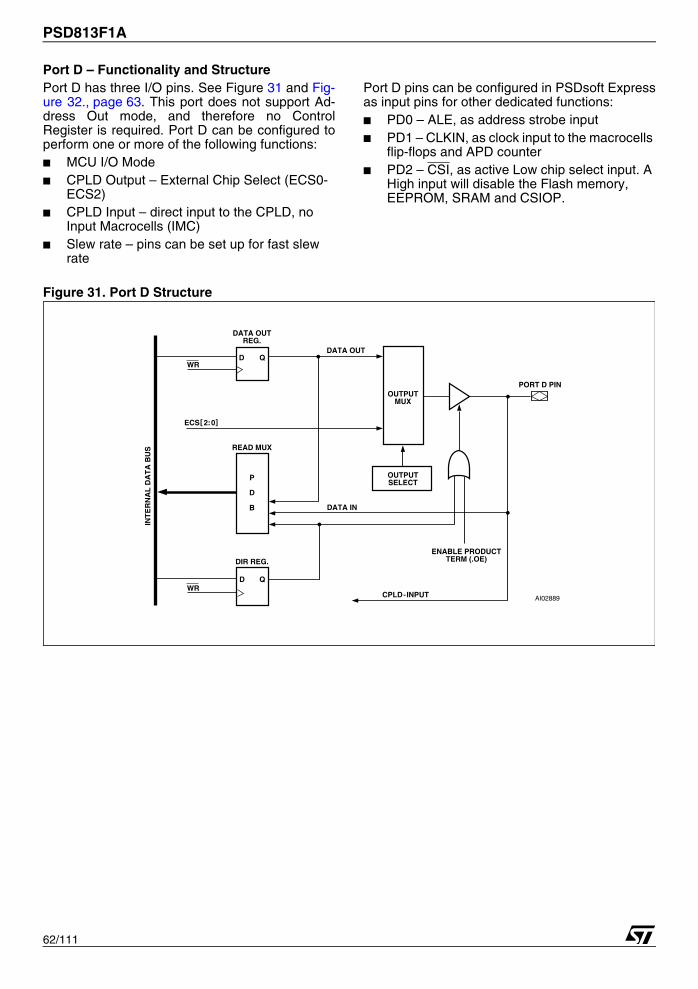
PSD813F1A
62/111
Port D – Functionality and StructurePort D has three I/O pins. See Figure 31 and Fig-ure 32., page 63. This port does not support Ad-dress Out mode, and therefore no ControlRegister is required. Port D can be configured toperform one or more of the following functions:■ MCU I/O Mode■ CPLD Output – External Chip Select (ECS0-
ECS2)■ CPLD Input – direct input to the CPLD, no
Input Macrocells (IMC)■ Slew rate – pins can be set up for fast slew
rate
Port D pins can be configured in PSDsoft Expressas input pins for other dedicated functions:■ PD0 – ALE, as address strobe input■ PD1 – CLKIN, as clock input to the macrocells
flip-flops and APD counter■ PD2 – CSI, as active Low chip select input. A
High input will disable the Flash memory, EEPROM, SRAM and CSIOP.
Figure 31. Port D Structure
INT
ER
NA
L D
AT
A B
US
DATA OUTREG.
D Q
D Q
WR
WR
ECS[ 2:0]
READ MUX
P
D
B
CPLD-INPUT
DIR REG.
DATA IN
ENABLE PRODUCTTERM (.OE)
OUTPUTSELECT
OUTPUTMUX
PORT D PIN
DATA OUT
AI02889
63/111
PSD813F1A
External Chip SelectThe CPLD also provides three External Chip Se-lect (ECS0-ECS2) outputs on Port D pins that canbe used to select external devices. Each ExternalChip Select (ECS0-ECS2) consists of one product
term that can be configured active High or Low.The output enable of the pin is controlled by eitherthe output enable product term or the DirectionRegister. (See Figure 32.)
Figure 32. Port D External Chip Select SignalsP
LD
IN
PU
T B
US
POLARITYBIT
PD2 PINPT2 ECS2
DIRECTIONREGISTER
POLARITYBIT
PD1 PINPT1 ECS1
ENABLE (.OE)
ENABLE (.OE) DIRECTIONREGISTER
POLARITYBIT
PD0 PINPT0 ECS0
ENABLE (.OE) DIRECTIONREGISTER
CP
LD
AN
D A
RR
AY
AI02890
PSD813F1A
64/111
POWER MANAGEMENTThe PSD offers configurable power saving op-tions. These options may be used individually or incombinations, as follows:– All memory types in a PSD (Flash, EEPROM,
and SRAM) are built with Zero-Power technology. In addition to using special silicon design methodology, Zero-Power technology puts the memories into standby mode when address/data inputs are not changing (zero DC current). As soon as a transition occurs on an input, the affected memory “wakes up”, changes and latches its outputs, then goes back to standby. The designer does not have to do anything special to achieve memory standby mode when no inputs are changing—it happens automatically.The PLD sections can also achieve standby mode when its inputs are not changing, as de-scribed in the section entitled PLD Power Management, page 66.
– Like the Zero-Power feature, the Automatic Power Down (APD) logic allows the PSD to reduce to standby current automatically. The APD will block MCU address/data signals from reaching the memories and PLDs. This feature is available on all PSD devices. The APD Unit is described in more detail in the sections entitled Automatic Power-down (APD) Unit and Power-down Mode, page 65.Built in logic will monitor the address strobe of the MCU for activity. If there is no activity for a certain time period (MCU is asleep), the APD logic initiates Power Down Mode (if enabled). Once in Power Down Mode, all address/data signals are blocked from reaching PSD memories and PLDs, and the memories are deselected internally. This allows the memories and PLDs to remain in standby mode even if the address/data lines are
changing state externally (noise, other devices on the MCU bus, etc.). Keep in mind that any unblocked PLD input signals that are changing states keeps the PLD out of standby mode, but not the memories.
– The PSD Chip Select Input (CSI) on all families can be used to disable the internal memories, placing them in standby mode even if inputs are changing. This feature does not block any internal signals or disable the PLDs. This is a good alternative to using the APD logic, especially if your MCU has a chip select output. There is a slight penalty in memory access time when the CSI signal makes its initial transition from deselected to selected.
– The PMMR registers can be written by the MCU at run-time to manage power. PSD supports “blocking bits” in these registers that are set to block designated signals from reaching both PLDs. Current consumption of the PLDs is directly related to the composite frequency of the changes on their inputs (see Figure 36., page 73 and Figure 37., page 73). Significant power savings can be achieved by blocking signals that are not used in DPLD or CPLD logic equations.The PSD has a Turbo Bit in the PMMR0 register. This bit can be set to disable the Turbo Mode feature (default is Turbo Mode on). While Turbo Mode is disabled, the PLDs can achieve standby current when no PLD inputs are changing (zero DC current). Even when inputs do change, significant power can be saved at lower frequencies (AC current), compared to when Turbo Mode is enabled. When the Turbo Mode is enabled, there is a significant DC current component and the AC component is higher.
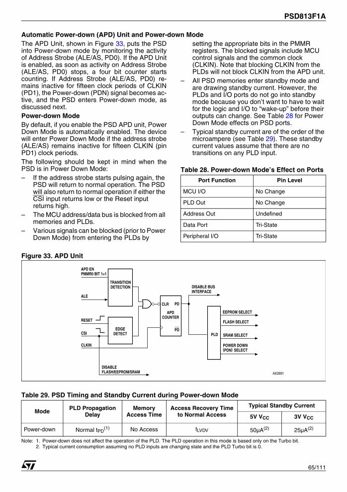
65/111
PSD813F1A
Automatic Power-down (APD) Unit and Power-down ModeThe APD Unit, shown in Figure 33, puts the PSDinto Power-down mode by monitoring the activityof Address Strobe (ALE/AS, PD0). If the APD Unitis enabled, as soon as activity on Address Strobe(ALE/AS, PD0) stops, a four bit counter startscounting. If Address Strobe (ALE/AS, PD0) re-mains inactive for fifteen clock periods of CLKIN(PD1), the Power-down (PDN) signal becomes ac-tive, and the PSD enters Power-down mode, asdiscussed next.Power-down ModeBy default, if you enable the PSD APD unit, PowerDown Mode is automatically enabled. The devicewill enter Power Down Mode if the address strobe(ALE/AS) remains inactive for fifteen CLKIN (pinPD1) clock periods.The following should be kept in mind when thePSD is in Power Down Mode:– If the address strobe starts pulsing again, the
PSD will return to normal operation. The PSD will also return to normal operation if either the CSI input returns low or the Reset input returns high.
– The MCU address/data bus is blocked from all memories and PLDs.
– Various signals can be blocked (prior to Power Down Mode) from entering the PLDs by
setting the appropriate bits in the PMMR registers. The blocked signals include MCU control signals and the common clock (CLKIN). Note that blocking CLKIN from the PLDs will not block CLKIN from the APD unit.
– All PSD memories enter standby mode and are drawing standby current. However, the PLDs and I/O ports do not go into standby mode because you don’t want to have to wait for the logic and I/O to “wake-up” before their outputs can change. See Table 28 for Power Down Mode effects on PSD ports.
– Typical standby current are of the order of the microampere (see Table 29). These standby current values assume that there are no transitions on any PLD input.
Table 28. Power-down Mode’s Effect on Ports
Figure 33. APD Unit
Table 29. PSD Timing and Standby Current during Power-down Mode
Note: 1. Power-down does not affect the operation of the PLD. The PLD operation in this mode is based only on the Turbo bit.2. Typical current consumption assuming no PLD inputs are changing state and the PLD Turbo bit is 0.
Port Function Pin Level
MCU I/O No Change
PLD Out No Change
Address Out Undefined
Data Port Tri-State
Peripheral I/O Tri-State
Mode PLD Propagation Delay
Memory Access Time
Access Recovery Time to Normal Access
Typical Standby Current
5V VCC 3V VCC
Power-down Normal tPD(1) No Access tLVDV 50µA(2) 25µA(2)
APD ENPMMR0 BIT 1=1
ALE
RESET
CSI
CLKIN
TRANSITIONDETECTION
EDGEDETECT
APDCOUNTER
POWER DOWN(PDN)
DISABLE BUSINTERFACE
EEPROM SELECT
FLASH SELECT
SRAM SELECT
PDCLR
PD
DISABLEFLASH/EEPROM/SRAM
PLD
SELECT
AI02891
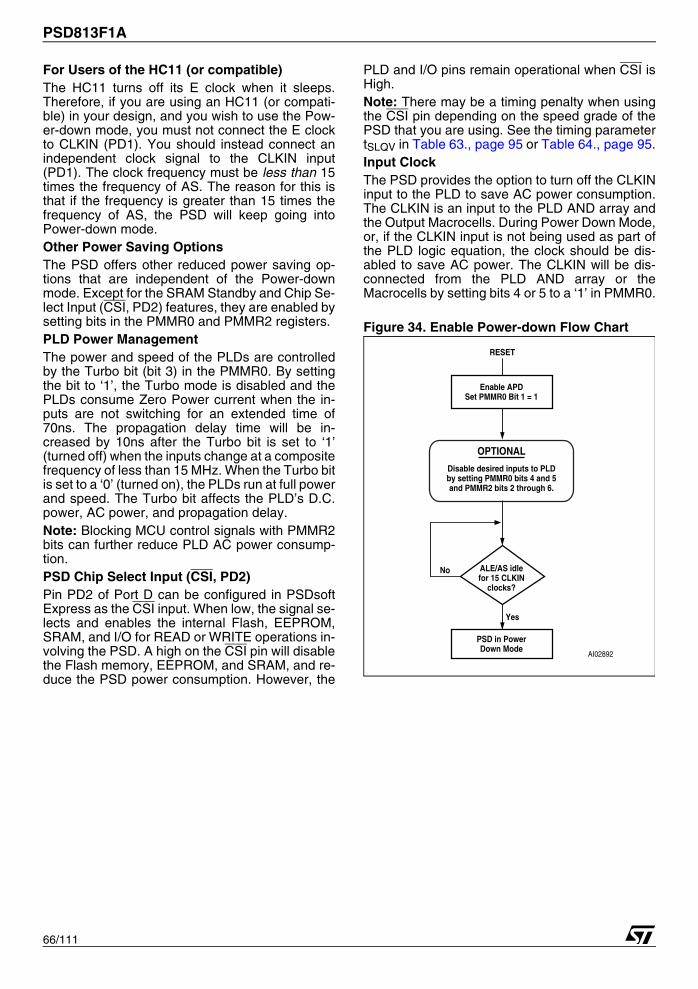
PSD813F1A
66/111
For Users of the HC11 (or compatible)The HC11 turns off its E clock when it sleeps.Therefore, if you are using an HC11 (or compati-ble) in your design, and you wish to use the Pow-er-down mode, you must not connect the E clockto CLKIN (PD1). You should instead connect anindependent clock signal to the CLKIN input(PD1). The clock frequency must be less than 15times the frequency of AS. The reason for this isthat if the frequency is greater than 15 times thefrequency of AS, the PSD will keep going intoPower-down mode.Other Power Saving OptionsThe PSD offers other reduced power saving op-tions that are independent of the Power-downmode. Except for the SRAM Standby and Chip Se-lect Input (CSI, PD2) features, they are enabled bysetting bits in the PMMR0 and PMMR2 registers.PLD Power ManagementThe power and speed of the PLDs are controlledby the Turbo bit (bit 3) in the PMMR0. By settingthe bit to ‘1’, the Turbo mode is disabled and thePLDs consume Zero Power current when the in-puts are not switching for an extended time of70ns. The propagation delay time will be in-creased by 10ns after the Turbo bit is set to ‘1’(turned off) when the inputs change at a compositefrequency of less than 15 MHz. When the Turbo bitis set to a ‘0’ (turned on), the PLDs run at full powerand speed. The Turbo bit affects the PLD’s D.C.power, AC power, and propagation delay.Note: Blocking MCU control signals with PMMR2bits can further reduce PLD AC power consump-tion.PSD Chip Select Input (CSI, PD2)Pin PD2 of Port D can be configured in PSDsoftExpress as the CSI input. When low, the signal se-lects and enables the internal Flash, EEPROM,SRAM, and I/O for READ or WRITE operations in-volving the PSD. A high on the CSI pin will disablethe Flash memory, EEPROM, and SRAM, and re-duce the PSD power consumption. However, the
PLD and I/O pins remain operational when CSI isHigh.Note: There may be a timing penalty when usingthe CSI pin depending on the speed grade of thePSD that you are using. See the timing parametertSLQV in Table 63., page 95 or Table 64., page 95.Input ClockThe PSD provides the option to turn off the CLKINinput to the PLD to save AC power consumption.The CLKIN is an input to the PLD AND array andthe Output Macrocells. During Power Down Mode,or, if the CLKIN input is not being used as part ofthe PLD logic equation, the clock should be dis-abled to save AC power. The CLKIN will be dis-connected from the PLD AND array or theMacrocells by setting bits 4 or 5 to a ‘1’ in PMMR0.
Figure 34. Enable Power-down Flow Chart
Enable APDSet PMMR0 Bit 1 = 1
PSD in PowerDown Mode
ALE/AS idlefor 15 CLKIN
clocks?
RESET
Yes
No
OPTIONAL
Disable desired inputs to PLDby setting PMMR0 bits 4 and 5and PMMR2 bits 2 through 6.
AI02892
67/111
PSD813F1A
Table 30. Power Management Mode Registers PMMR0 (Note 1)
Note: 1. The bits of this register are cleared to zero following Power-up. Subsequent Reset (RESET) pulses do not clear the registers.
Table 31. Power Management Mode Registers PMMR2 (Note 1)
Note: 1. The bits of this register are cleared to zero following Power-up. Subsequent Reset (RESET) pulses do not clear the registers.
Bit 0 X 0 Not used, and should be set to zero.
Bit 1 APD Enable0 = off Automatic Power-down (APD) is disabled.
1 = on Automatic Power-down (APD) is enabled.
Bit 2 X 0 Not used, and should be set to zero.
Bit 3 PLD Turbo0 = on PLD Turbo mode is on
1 = off PLD Turbo mode is off, saving power.
Bit 4 PLD Array clk0 = on CLKIN (PD1) input to the PLD AND Array is connected. Every change of CLKIN
(PD1) Powers-up the PLD when Turbo bit is 0.
1 = off CLKIN (PD1) input to PLD AND Array is disconnected, saving power.
Bit 5 PLD MCell clk0 = on CLKIN (PD1) input to the PLD macrocells is connected.
1 = off CLKIN (PD1) input to PLD macrocells is disconnected, saving power.
Bit 6 X 0 Not used, and should be set to zero.
Bit 7 X 0 Not used, and should be set to zero.
Bit 0 X 0 Not used, and should be set to zero.
Bit 1 X 0 Not used, and should be set to zero.
Bit 2PLD Array CNTL0
0 = on Cntl0 input to the PLD AND Array is connected.
1 = off Cntl0 input to PLD AND Array is disconnected, saving power.
Bit 3 PLD Array CNTL1
0 = on Cntl1 input to the PLD AND Array is connected.
1 = off Cntl1 input to PLD AND Array is disconnected, saving power.
Bit 4PLD Array CNTL2
0 = on Cntl2 input to the PLD AND Array is connected.
1 = off Cntl2 input to PLD AND Array is disconnected, saving power.
Bit 5 PLD Array ALE
0 = on ALE input to the PLD AND Array is connected.
1 = off ALE input to PLD AND Array is disconnected, saving power.
Bit 6PLD Array DBE
0 = on DBE input to the PLD AND Array is connected.
1 = off DBE input to PLD AND Array is disconnected, saving power.
Bit 7 X 0 Not used, and should be set to zero.
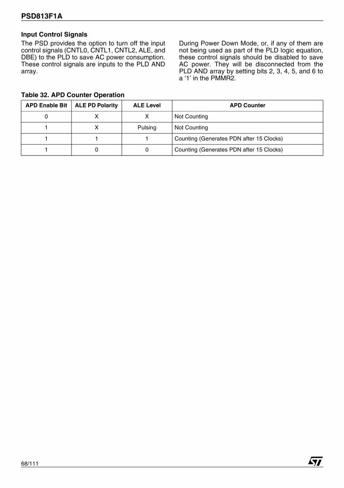
PSD813F1A
68/111
Input Control SignalsThe PSD provides the option to turn off the inputcontrol signals (CNTL0, CNTL1, CNTL2, ALE, andDBE) to the PLD to save AC power consumption.These control signals are inputs to the PLD ANDarray.
During Power Down Mode, or, if any of them arenot being used as part of the PLD logic equation,these control signals should be disabled to saveAC power. They will be disconnected from thePLD AND array by setting bits 2, 3, 4, 5, and 6 toa ‘1’ in the PMMR2.
Table 32. APD Counter Operation
APD Enable Bit ALE PD Polarity ALE Level APD Counter
0 X X Not Counting
1 X Pulsing Not Counting
1 1 1 Counting (Generates PDN after 15 Clocks)
1 0 0 Counting (Generates PDN after 15 Clocks)
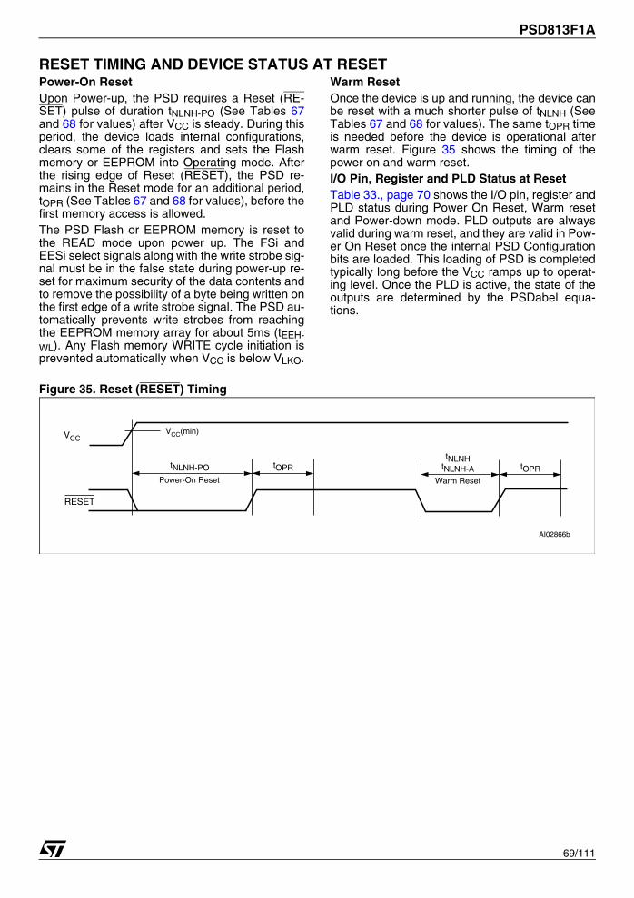
69/111
PSD813F1A
RESET TIMING AND DEVICE STATUS AT RESETPower-On ResetUpon Power-up, the PSD requires a Reset (RE-SET) pulse of duration tNLNH-PO (See Tables 67and 68 for values) after VCC is steady. During thisperiod, the device loads internal configurations,clears some of the registers and sets the Flashmemory or EEPROM into Operating mode. Afterthe rising edge of Reset (RESET), the PSD re-mains in the Reset mode for an additional period,tOPR (See Tables 67 and 68 for values), before thefirst memory access is allowed.The PSD Flash or EEPROM memory is reset tothe READ mode upon power up. The FSi andEESi select signals along with the write strobe sig-nal must be in the false state during power-up re-set for maximum security of the data contents andto remove the possibility of a byte being written onthe first edge of a write strobe signal. The PSD au-tomatically prevents write strobes from reachingthe EEPROM memory array for about 5ms (tEEH-WL). Any Flash memory WRITE cycle initiation isprevented automatically when VCC is below VLKO.
Warm ResetOnce the device is up and running, the device canbe reset with a much shorter pulse of tNLNH (SeeTables 67 and 68 for values). The same tOPR timeis needed before the device is operational afterwarm reset. Figure 35 shows the timing of thepower on and warm reset.I/O Pin, Register and PLD Status at ResetTable 33., page 70 shows the I/O pin, register andPLD status during Power On Reset, Warm resetand Power-down mode. PLD outputs are alwaysvalid during warm reset, and they are valid in Pow-er On Reset once the internal PSD Configurationbits are loaded. This loading of PSD is completedtypically long before the VCC ramps up to operat-ing level. Once the PLD is active, the state of theoutputs are determined by the PSDabel equa-tions.
Figure 35. Reset (RESET) Timing
tNLNH-PO tOPR
AI02866b
RESET
tNLNHtNLNH-A tOPR
VCCVCC(min)
Power-On Reset Warm Reset
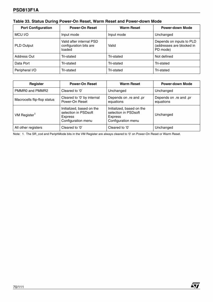
PSD813F1A
70/111
Table 33. Status During Power-On Reset, Warm Reset and Power-down Mode
Note: 1. The SR_cod and PeriphMode bits in the VM Register are always cleared to ‘0’ on Power-On Reset or Warm Reset.
Port Configuration Power-On Reset Warm Reset Power-down Mode
MCU I/O Input mode Input mode Unchanged
PLD Output Valid after internal PSD configuration bits are loaded
Valid Depends on inputs to PLD (addresses are blocked in PD mode)
Address Out Tri-stated Tri-stated Not defined
Data Port Tri-stated Tri-stated Tri-stated
Peripheral I/O Tri-stated Tri-stated Tri-stated
Register Power-On Reset Warm Reset Power-down Mode
PMMR0 and PMMR2 Cleared to ‘0’ Unchanged Unchanged
Macrocells flip-flop status Cleared to ‘0’ by internal Power-On Reset
Depends on .re and .pr equations
Depends on .re and .pr equations
VM Register1
Initialized, based on the selection in PSDsoft ExpressConfiguration menu
Initialized, based on the selection in PSDsoft ExpressConfiguration menu
Unchanged
All other registers Cleared to ‘0’ Cleared to ‘0’ Unchanged
71/111
PSD813F1A
PROGRAMMING IN-CIRCUIT USING THE JTAG SERIAL INTERFACEThe JTAG interface on the PSD can be enabled onPort C (see Table 34., page 72). All memory(Flash and EEPROM), PLD logic, and PSD config-uration bits may be programmed through theJTAG interface. A blank part can be mounted on aprinted circuit board and programmed usingJTAG.The standard JTAG signals (IEEE 1149.1) areTMS, TCK, TDI, and TDO. Two additional signals,TSTAT and TERR, are optional JTAG extensionsused to speed up program and erase operations.Note: By default, on a blank PSD (as shipped fromfactory or after erasure), four pins on Port C areenabled for the basic JTAG signals TMS, TCK,TDI, and TDO.Standard JTAG SignalsThe standard JTAG signals (TMS, TCK, TDI, andTDO) can be enabled by any of three different con-ditions that are logically ORed. When enabled,TDI, TDO, TCK, and TMS are inputs, waiting for aserial command from an external JTAG controllerdevice (such as FlashLink or Automated TestEquipment). When the enabling command is re-ceived from the external JTAG controller, TDO be-comes an output and the JTAG channel is fullyfunctional inside the PSD. The same commandthat enables the JTAG channel may optionally en-able the two additional JTAG pins, TSTAT andTERR.The following symbolic logic equation specifies theconditions enabling the four basic JTAG pins(TMS, TCK, TDI, and TDO) on their respectivePort C pins. For purposes of discussion, the logiclabel JTAG_ON will be used. When JTAG_ON istrue, the four pins are enabled for JTAG. WhenJTAG_ON is false, the four pins can be used forgeneral PSD I/O.
JTAG_ON = PSDsoft_enabled +/* An NVM configuration bit inside the PSD
is set by the designer in the PSDsoft Express Configuration utility. This dedicates the pins for JTAG at all times (compliant with IEEE 1149.1) */
Microcontroller_enabled +/* The microcontroller can set a bit at run-
time by writing to the PSD register, JTAG Enable. This register is located at address CSIOP + offset C7h. Setting the JTAG_ENABLE bit in this register will enable the pins for JTAG use. This bit is cleared by a PSD reset or the microcontroller. See Table 35., page 72 for bit definition. */
PSD_product_term_enabled;/* A dedicated product term (PT) inside the
PSD can be used to enable the JTAG pins. This PT has the reserved name JTAGSEL. Once defined as a node in PSDabel, the designer can write an equation for JTAGSEL. This method is used when the Port C JTAG pins are multiplexed with other I/O signals. It is recommended to logically tie the node JTAGSEL to the JEN\ signal on the Flashlink cable when multiplexing JTAG signals. (AN1153)
The PSD supports JTAG In-System-Configuration(ISC) commands, but not Boundary Scan. A defi-nition of these JTAG-ISC commands and se-quences are defined in a supplemental documentavailable from ST. ST’s PSDsoft Express softwaretool and FlashLink JTAG programming cable im-plement these JTAG-ISC commands. This docu-ment is needed only as a reference for designerswho use a FlashLink to program their PSD.
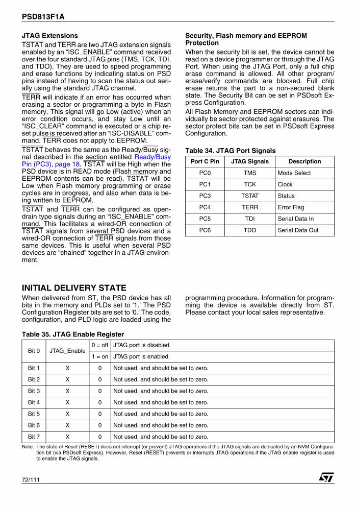
PSD813F1A
72/111
JTAG ExtensionsTSTAT and TERR are two JTAG extension signalsenabled by an “ISC_ENABLE” command receivedover the four standard JTAG pins (TMS, TCK, TDI,and TDO). They are used to speed programmingand erase functions by indicating status on PSDpins instead of having to scan the status out seri-ally using the standard JTAG channel.TERR will indicate if an error has occurred whenerasing a sector or programming a byte in Flashmemory. This signal will go Low (active) when anerror condition occurs, and stay Low until an“ISC_CLEAR” command is executed or a chip re-set pulse is received after an “ISC-DISABLE” com-mand. TERR does not apply to EEPROM.TSTAT behaves the same as the Ready/Busy sig-nal described in the section entitled Ready/BusyPin (PC3), page 18. TSTAT will be High when thePSD device is in READ mode (Flash memory andEEPROM contents can be read). TSTAT will beLow when Flash memory programming or erasecycles are in progress, and also when data is be-ing written to EEPROM.TSTAT and TERR can be configured as open-drain type signals during an “ISC_ENABLE” com-mand. This facilitates a wired-OR connection ofTSTAT signals from several PSD devices and awired-OR connection of TERR signals from thosesame devices. This is useful when several PSDdevices are “chained” together in a JTAG environ-ment.
Security, Flash memory and EEPROM ProtectionWhen the security bit is set, the device cannot beread on a device programmer or through the JTAGPort. When using the JTAG Port, only a full chiperase command is allowed. All other program/erase/verify commands are blocked. Full chiperase returns the part to a non-secured blankstate. The Security Bit can be set in PSDsoft Ex-press Configuration.All Flash Memory and EEPROM sectors can indi-vidually be sector protected against erasures. Thesector protect bits can be set in PSDsoft ExpressConfiguration.
Table 34. JTAG Port Signals
INITIAL DELIVERY STATEWhen delivered from ST, the PSD device has allbits in the memory and PLDs set to '1.' The PSDConfiguration Register bits are set to '0.' The code,configuration, and PLD logic are loaded using the
programming procedure. Information for program-ming the device is available directly from ST.Please contact your local sales representative.
Table 35. JTAG Enable Register
Note: The state of Reset (RESET) does not interrupt (or prevent) JTAG operations if the JTAG signals are dedicated by an NVM Configura-tion bit (via PSDsoft Express). However, Reset (RESET) prevents or interrupts JTAG operations if the JTAG enable register is usedto enable the JTAG signals.
Port C Pin JTAG Signals Description
PC0 TMS Mode Select
PC1 TCK Clock
PC3 TSTAT Status
PC4 TERR Error Flag
PC5 TDI Serial Data In
PC6 TDO Serial Data Out
Bit 0 JTAG_Enable0 = off JTAG port is disabled.
1 = on JTAG port is enabled.
Bit 1 X 0 Not used, and should be set to zero.
Bit 2 X 0 Not used, and should be set to zero.
Bit 3 X 0 Not used, and should be set to zero.
Bit 4 X 0 Not used, and should be set to zero.
Bit 5 X 0 Not used, and should be set to zero.
Bit 6 X 0 Not used, and should be set to zero.
Bit 7 X 0 Not used, and should be set to zero.

73/111
PSD813F1A
AC/DC PARAMETERSThe following tables describe the AD and DC pa-rameters of the PSD:■ DC Electrical Specification■ AC Timing Specification
PLD Timing– Combinatorial Timing– Synchronous Clock Mode– Asynchronous Clock Mode– Input Macrocell TimingMCU Timing– READ Timing– WRITE Timing– Peripheral Mode Timing– Power-down and Reset Timing
The following are issues concerning the parame-ters presented:■ In the DC specification the supply current is
given for different modes of operation. Before calculating the total power consumption, determine the percentage of time that the PSD is in each mode. Also, the supply power is considerably different if the Turbo bit is ‘0.’
■ The AC power component gives the PLD, EEPROM and SRAM mA/MHz specification. Figures 36 and 37 show the PLD mA/MHz as a function of the number of Product Terms (PT) used.
■ In the PLD timing parameters, add the required delay when Turbo bit is ‘0.'
Figure 36. PLD ICC /Frequency Consumption (5V range)
Figure 37. PLD ICC /Frequency Consumption (3V range)
0
10
20
30
40
60
70
80
90
100
110
VCC = 5V
50
0 10 155 20 25
HIGHEST COMPOSITE FREQUENCY AT PLD INPUTS (MHz)
I CC
– (
mA
)
TURBO ON (100%)
TURBO ON (25%)
TURBO O
FF
TURBO OFF PT 100%PT 25%
AI02894
0
10
20
30
40
50
60VCC = 3V
0 10 155 20 25
I CC
– (
mA
)
TURBO ON (100%)
TURBO ON (25%)
TURBO O
FF
TURBO OFF
HIGHEST COMPOSITE FREQUENCY AT PLD INPUTS (MHz)
PT 100%PT 25%
AI03100
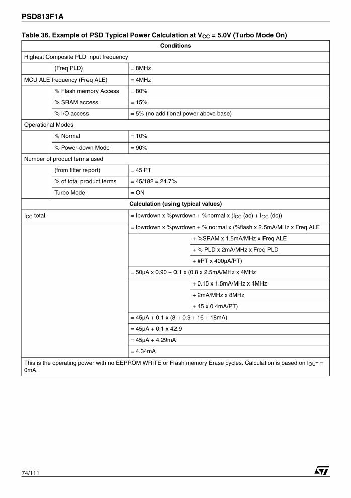
PSD813F1A
74/111
Table 36. Example of PSD Typical Power Calculation at VCC = 5.0V (Turbo Mode On)
Conditions
Highest Composite PLD input frequency
(Freq PLD) = 8MHz
MCU ALE frequency (Freq ALE) = 4MHz
% Flash memory Access = 80%
% SRAM access = 15%
% I/O access = 5% (no additional power above base)
Operational Modes
% Normal = 10%
% Power-down Mode = 90%
Number of product terms used
(from fitter report) = 45 PT
% of total product terms = 45/182 = 24.7%
Turbo Mode = ON
Calculation (using typical values)
ICC total = Ipwrdown x %pwrdown + %normal x (ICC (ac) + ICC (dc))
= Ipwrdown x %pwrdown + % normal x (%flash x 2.5mA/MHz x Freq ALE
+ %SRAM x 1.5mA/MHz x Freq ALE
+ % PLD x 2mA/MHz x Freq PLD
+ #PT x 400µA/PT)
= 50µA x 0.90 + 0.1 x (0.8 x 2.5mA/MHz x 4MHz
+ 0.15 x 1.5mA/MHz x 4MHz
+ 2mA/MHz x 8MHz
+ 45 x 0.4mA/PT)
= 45µA + 0.1 x (8 + 0.9 + 16 + 18mA)
= 45µA + 0.1 x 42.9
= 45µA + 4.29mA
= 4.34mA
This is the operating power with no EEPROM WRITE or Flash memory Erase cycles. Calculation is based on IOUT = 0mA.
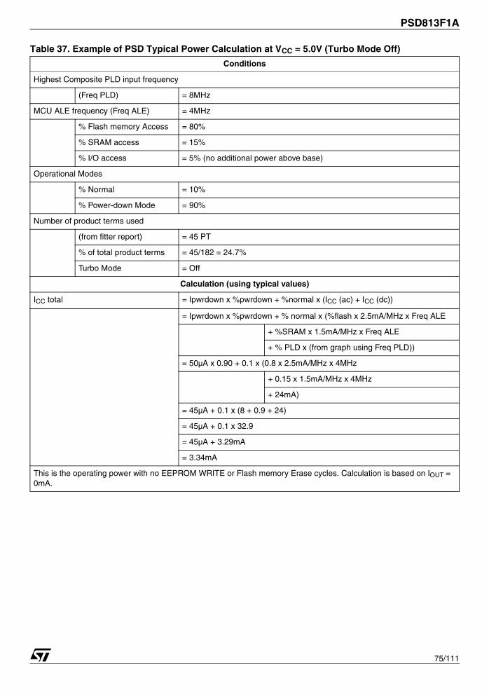
75/111
PSD813F1A
Table 37. Example of PSD Typical Power Calculation at VCC = 5.0V (Turbo Mode Off)
Conditions
Highest Composite PLD input frequency
(Freq PLD) = 8MHz
MCU ALE frequency (Freq ALE) = 4MHz
% Flash memory Access = 80%
% SRAM access = 15%
% I/O access = 5% (no additional power above base)
Operational Modes
% Normal = 10%
% Power-down Mode = 90%
Number of product terms used
(from fitter report) = 45 PT
% of total product terms = 45/182 = 24.7%
Turbo Mode = Off
Calculation (using typical values)
ICC total = Ipwrdown x %pwrdown + %normal x (ICC (ac) + ICC (dc))
= Ipwrdown x %pwrdown + % normal x (%flash x 2.5mA/MHz x Freq ALE
+ %SRAM x 1.5mA/MHz x Freq ALE
+ % PLD x (from graph using Freq PLD))
= 50µA x 0.90 + 0.1 x (0.8 x 2.5mA/MHz x 4MHz
+ 0.15 x 1.5mA/MHz x 4MHz
+ 24mA)
= 45µA + 0.1 x (8 + 0.9 + 24)
= 45µA + 0.1 x 32.9
= 45µA + 3.29mA
= 3.34mA
This is the operating power with no EEPROM WRITE or Flash memory Erase cycles. Calculation is based on IOUT = 0mA.
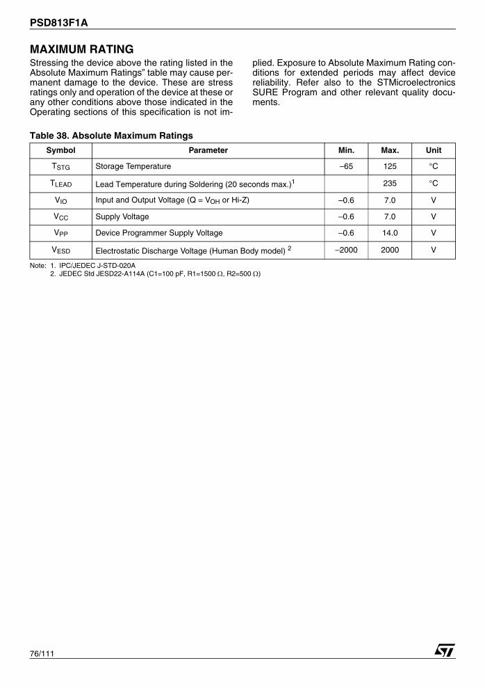
PSD813F1A
76/111
MAXIMUM RATINGStressing the device above the rating listed in theAbsolute Maximum Ratings” table may cause per-manent damage to the device. These are stressratings only and operation of the device at these orany other conditions above those indicated in theOperating sections of this specification is not im-
plied. Exposure to Absolute Maximum Rating con-ditions for extended periods may affect devicereliability. Refer also to the STMicroelectronicsSURE Program and other relevant quality docu-ments.
Table 38. Absolute Maximum Ratings
Note: 1. IPC/JEDEC J-STD-020A2. JEDEC Std JESD22-A114A (C1=100 pF, R1=1500 Ω, R2=500 Ω)
Symbol Parameter Min. Max. Unit
TSTG Storage Temperature –65 125 °C
TLEAD Lead Temperature during Soldering (20 seconds max.)1 235 °C
VIO Input and Output Voltage (Q = VOH or Hi-Z) –0.6 7.0 V
VCC Supply Voltage –0.6 7.0 V
VPP Device Programmer Supply Voltage –0.6 14.0 V
VESD Electrostatic Discharge Voltage (Human Body model) 2 –2000 2000 V
77/111
PSD813F1A
DC AND AC PARAMETERSThis section summarizes the operating and mea-surement conditions, and the DC and AC charac-teristics of the device. The parameters in the DCand AC Characteristic tables that follow are de-rived from tests performed under the Measure-
ment Conditions summarized in the relevanttables. Designers should check that the operatingconditions in their circuit match the measurementconditions when relying on the quoted parame-ters.
Table 39. Operating Conditions (5V devices)
Table 40. Operating Conditions (3V devices)
Table 41. AC Signal Letters for PLD Timings
Note: Example: tAVLX = Time from Address Valid to ALE Invalid.
Table 42. AC Signal Behavior Symbols for PLD Timings
Note: Example: tAVLX = Time from Address Valid to ALE Invalid.
Table 43. AC Measurement Conditions
Note: 1. Output Hi-Z is defined as the point where data out is no longer driven.
Symbol Parameter Min. Max. Unit
VCC Supply Voltage 4.5 5.5 V
TAAmbient Operating Temperature (Industrial) –40 85 °C
Ambient Operating Temperature (Commercial) 0 70 °C
Symbol Parameter Min. Max. Unit
VCC Supply Voltage 3.0 3.6 V
TAAmbient Operating Temperature (Industrial) –40 85 °C
Ambient Operating Temperature (Commercial) 0 70 °C
A Address Input
C CEout Output
D Input Data
E E Input
G Internal WDOG_ON signal
I Interrupt Input
L ALE Input
N Reset Input or Output
P Port Signal Output
Q Output Data
R WR, UDS, LDS, DS, IORD, PSEN Inputs
S Chip Select Input
T R/W Input
W Internal PDN Signal
M Output Macrocell
t Time
L Logic Level Low or ALE
H Logic Level High
V Valid
X No Longer a Valid Logic Level
Z Float
PW Pulse Width
Symbol Parameter Min. Max. Unit
CL Load Capacitance 30 pF
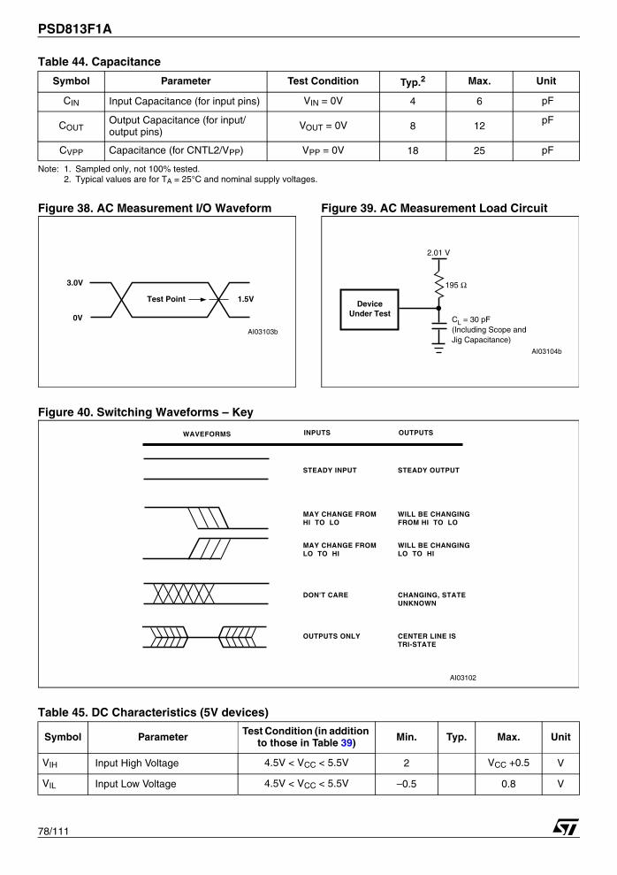
PSD813F1A
78/111
Table 44. Capacitance
Note: 1. Sampled only, not 100% tested.2. Typical values are for TA = 25°C and nominal supply voltages.
Figure 38. AC Measurement I/O Waveform Figure 39. AC Measurement Load Circuit
Figure 40. Switching Waveforms – Key
Table 45. DC Characteristics (5V devices)
Symbol Parameter Test Condition Typ.2 Max. Unit
CIN Input Capacitance (for input pins) VIN = 0V 4 6 pF
COUTOutput Capacitance (for input/output pins)
VOUT = 0V 8 12 pF
CVPP Capacitance (for CNTL2/VPP) VPP = 0V 18 25 pF
3.0V
0V
Test Point 1.5V
AI03103b
DeviceUnder Test
2.01 V
195 Ω
CL = 30 pF(Including Scope andJig Capacitance)
AI03104b
Symbol Parameter Test Condition (in addition to those in Table 39) Min. Typ. Max. Unit
VIH Input High Voltage 4.5V < VCC < 5.5V 2 VCC +0.5 V
VIL Input Low Voltage 4.5V < VCC < 5.5V –0.5 0.8 V
WAVEFORMS INPUTS OUTPUTS
STEADY INPUT
MAY CHANGE FROMHI TO LO
MAY CHANGE FROMLO TO HI
DON'T CARE
OUTPUTS ONLY
STEADY OUTPUT
WILL BE CHANGINGFROM HI TO LO
WILL BE CHANGINGLO TO HI
CHANGING, STATEUNKNOWN
CENTER LINE ISTRI-STATE
AI03102
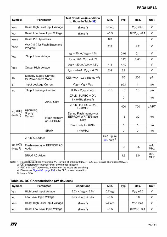
79/111
PSD813F1A
Note: 1. Reset (RESET) has hysteresis. VIL1 is valid at or below 0.2VCC –0.1. VIH1 is valid at or above 0.8VCC.2. CSI deselected or internal Power-down mode is active.3. PLD is in non-Turbo mode, and none of the inputs are switching.4. Please see Figure 36., page 73 for the PLD current calculation.5. IOUT = 0mA
Table 46. DC Characteristics (3V devices)
VIH1 Reset High Level Input Voltage (Note 1) 0.8VCC VCC +0.5 V
VIL1 Reset Low Level Input Voltage (Note 1) –0.5 0.2VCC –0.1 V
VHYS Reset Pin Hysteresis 0.3 V
VLKOVCC (min) for Flash Erase and Program
2.5 4.2 V
VOL Output Low VoltageIOL = 20µA, VCC = 4.5V 0.01 0.1 V
IOL = 8mA, VCC = 4.5V 0.25 0.45 V
VOH Output High VoltageIOH = –20µA, VCC = 4.5V 4.4 4.49 V
IOH = –2mA, VCC = 4.5V 2.4 3.9 V
ISBStandby Supply Currentfor Power-down Mode CSI >VCC –0.3V (Notes 2,3) 50 200 µA
ILI Input Leakage Current VSS < VIN < VCC –1 ±0.1 1 µA
ILO Output Leakage Current 0.45 < VOUT < VCC –10 ±5 10 µA
ICC (DC)
(Note 5)
OperatingSupply Current
ZPLD Only
ZPLD_TURBO = Off,f = 0MHz (Note 5)
0 mA
ZPLD_TURBO = On,f = 0MHz 400 700 µA/PT
Flash memory or EEPROM
During Flash memory or EEPROM WRITE/Erase
Only15 30 mA
Read only, f = 0MHz 0 0 mA
SRAM f = 0MHz 0 0 mA
ICC (AC)
(Note 5)
ZPLD AC AdderSee Figure 36, note 4
Flash memory or EEPROM AC Adder 2.5 3.5 mA/
MHz
SRAM AC Adder 1.5 3.0 mA/MHz
Symbol Parameter Conditions Min. Typ. Max. Unit
VIH High Level Input Voltage 3.0V < VCC < 3.6V 0.7VCC VCC +0.5 V
VIL Low Level Input Voltage 3.0V < VCC < 3.6V –0.5 0.8 V
VIH1 Reset High Level Input Voltage (Note 1) 0.8VCC VCC +0.5 V
VIL1 Reset Low Level Input Voltage (Note 1) –0.5 0.2VCC –0.1 V
Symbol Parameter Test Condition (in addition to those in Table 39) Min. Typ. Max. Unit

PSD813F1A
80/111
Note: 1. Reset (RESET) has hysteresis. VIL1 is valid at or below 0.2VCC –0.1. VIH1 is valid at or above 0.8VCC.2. CSI deselected or internal PD is active.3. IOUT = 0mA
Figure 41. Input to Output Disable / Enable
VHYS Reset Pin Hysteresis 0.3 V
VLKOVCC (min) for Flash Erase and Program
1.5 2.2 V
VOL Output Low VoltageIOL = 20µA, VCC = 3.0V 0.01 0.1 V
IOL = 4mA, VCC = 3.0V 0.15 0.45 V
VOH Output High Voltage IOH = –20µA, VCC = 3.0V 2.9 2.99 V
IOH = –1mA, VCC = 3.0V 2.7 2.8 V
ISBStandby Supply Currentfor Power-down Mode CSI >VCC –0.3V (Notes 2) 25 100 µA
ILI Input Leakage Current VSS < VIN < VCC –1 ±0.1 1 µA
ILO Output Leakage Current 0.45 < VIN < VCC –10 ±5 10 µA
ICC (DC)
(Note 3)
OperatingSupply Current
ZPLD Only
ZPLD_TURBO = Off,f = 0MHz (Note 3)
0 µA/PT
ZPLD_TURBO = On,f = 0MHz
200 400 µA/PT
Flash memory or EEPROM
During Flash memory or EEPROM WRITE/Erase
Only10 25 mA
Read only, f = 0MHz 0 0 mA
SRAM f = 0MHz 0 0 mA
ICC (AC)
(Note 3)
ZPLD AC Adder See Figure 37., page 73
Flash memory or EEPROM AC Adder 1.5 2.0
mA/MHz
SRAM AC Adder 0.8 1.5 mA/MHz
Symbol Parameter Conditions Min. Typ. Max. Unit
tER tEA
INPUT
INPUT TOOUTPUT
ENABLE/DISABLE
AI02863
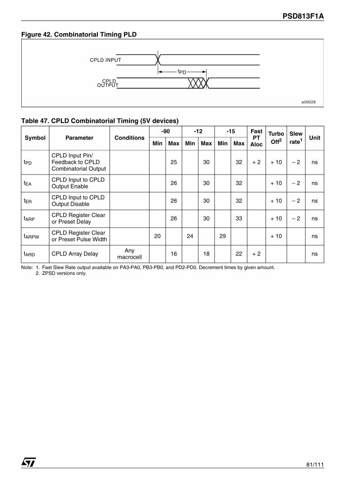
81/111
PSD813F1A
Figure 42. Combinatorial Timing PLD
Table 47. CPLD Combinatorial Timing (5V devices)
Note: 1. Fast Slew Rate output available on PA3-PA0, PB3-PB0, and PD2-PD0. Decrement times by given amount.2. ZPSD versions only.
Symbol Parameter Conditions-90 -12 -15 Fast
PTAloc
TurboOff2
Slewrate1 Unit
Min Max Min Max Min Max
tPD
CPLD Input Pin/Feedback to CPLD Combinatorial Output
25 30 32 + 2 + 10 – 2 ns
tEACPLD Input to CPLD Output Enable 26 30 32 + 10 – 2 ns
tERCPLD Input to CPLD Output Disable 26 30 32 + 10 – 2 ns
tARPCPLD Register Clear or Preset Delay 26 30 33 + 10 – 2 ns
tARPWCPLD Register Clear or Preset Pulse Width 20 24 29 + 10 ns
tARD CPLD Array Delay Any macrocell 16 18 22 + 2 ns
tPD
CPLD INPUT
CPLDOUTPUT
ai09228
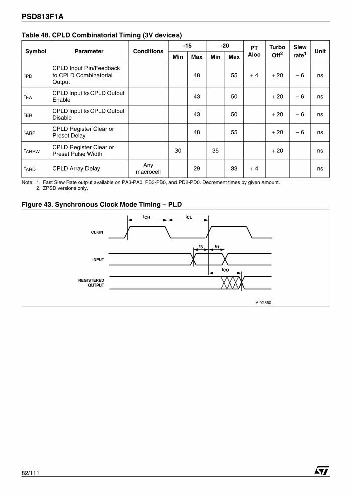
PSD813F1A
82/111
Table 48. CPLD Combinatorial Timing (3V devices)
Note: 1. Fast Slew Rate output available on PA3-PA0, PB3-PB0, and PD2-PD0. Decrement times by given amount.2. ZPSD versions only.
Figure 43. Synchronous Clock Mode Timing – PLD
Symbol Parameter Conditions-15 -20 PT
AlocTurboOff2
Slewrate1 Unit
Min Max Min Max
tPD
CPLD Input Pin/Feedback to CPLD Combinatorial Output
48 55 + 4 + 20 – 6 ns
tEACPLD Input to CPLD Output Enable 43 50 + 20 – 6 ns
tERCPLD Input to CPLD Output Disable 43 50 + 20 – 6 ns
tARPCPLD Register Clear or Preset Delay 48 55 + 20 – 6 ns
tARPWCPLD Register Clear or Preset Pulse Width 30 35 + 20 ns
tARD CPLD Array DelayAny
macrocell 29 33 + 4 ns
tCH tCL
tCO
tHtS
CLKIN
INPUT
REGISTEREDOUTPUT
AI02860
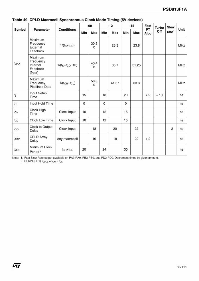
83/111
PSD813F1A
Table 49. CPLD Macrocell Synchronous Clock Mode Timing (5V devices)
Note: 1. Fast Slew Rate output available on PA3-PA0, PB3-PB0, and PD2-PD0. Decrement times by given amount.2. CLKIN (PD1) tCLCL = tCH + tCL.
Symbol Parameter Conditions-90 -12 -15 Fast
PTAloc
TurboOff
Slew rate1 Unit
Min Max Min Max Min Max
fMAX
Maximum FrequencyExternal Feedback
1/(tS+tCO) 30.30 26.3 23.8 MHz
Maximum FrequencyInternal Feedback(fCNT)
1/(tS+tCO–10) 43.48 35.7 31.25 MHz
Maximum FrequencyPipelined Data
1/(tCH+tCL) 50.00 41.67 33.3 MHz
tSInput Setup Time
15 18 20 + 2 + 10 ns
tH Input Hold Time 0 0 0 ns
tCHClock High Time Clock Input 10 12 15 ns
tCL Clock Low Time Clock Input 10 12 15 ns
tCOClock to Output Delay Clock Input 18 20 22 – 2 ns
tARDCPLD Array Delay Any macrocell 16 18 22 + 2 ns
tMINMinimum Clock Period 2 tCH+tCL 20 24 30 ns

PSD813F1A
84/111
Table 50. CPLD Macrocell Synchronous Clock Mode Timing (3V devices)
Note: 1. Fast Slew Rate output available on PA3-PA0, PB3-PB0, and PD2-PD0.2. CLKIN (PD1) tCLCL = tCH + tCL.
Figure 44. Asynchronous Reset / Preset
Figure 45. Asynchronous Clock Mode Timing (Product Term Clock)
Symbol Parameter Conditions-15 -20 PT
AlocTurbo
OffSlew rate1 Unit
Min Max Min Max
fMAX
Maximum FrequencyExternal Feedback
1/(tS+tCO) 17.8 14.7 MHz
Maximum FrequencyInternal Feedback (fCNT) 1/(tS+tCO–10) 19.6 17.2 MHz
Maximum FrequencyPipelined Data
1/(tCH+tCL) 33.3 31.2 MHz
tS Input Setup Time 27 35 + 4 + 20 ns
tH Input Hold Time 0 0 ns
tCH Clock High Time Clock Input 15 16 ns
tCL Clock Low Time Clock Input 15 16 ns
tCO Clock to Output Delay Clock Input 35 39 – 6 ns
tARD CPLD Array Delay Any macrocell 29 33 + 4 ns
tMIN Minimum Clock Period2 tCH+tCL 29 32 ns
tARP
REGISTEROUTPUT
tARPW
RESET/PRESETINPUT
AI02864
tCHA tCLA
tCOA
tHAtSA
CLOCK
INPUT
REGISTEREDOUTPUT
AI02859
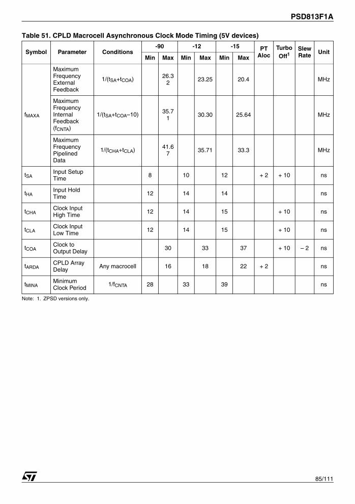
85/111
PSD813F1A
Table 51. CPLD Macrocell Asynchronous Clock Mode Timing (5V devices)
Note: 1. ZPSD versions only.
Symbol Parameter Conditions-90 -12 -15 PT
AlocTurboOff1
SlewRate Unit
Min Max Min Max Min Max
fMAXA
Maximum FrequencyExternal Feedback
1/(tSA+tCOA) 26.32 23.25 20.4 MHz
Maximum FrequencyInternal Feedback (fCNTA)
1/(tSA+tCOA–10) 35.71 30.30 25.64 MHz
Maximum FrequencyPipelined Data
1/(tCHA+tCLA) 41.67
35.71 33.3 MHz
tSAInput Setup Time 8 10 12 + 2 + 10 ns
tHAInput Hold Time 12 14 14 ns
tCHAClock Input High Time 12 14 15 + 10 ns
tCLAClock Input Low Time 12 14 15 + 10 ns
tCOAClock to Output Delay 30 33 37 + 10 – 2 ns
tARDACPLD Array Delay Any macrocell 16 18 22 + 2 ns
tMINAMinimum Clock Period
1/fCNTA 28 33 39 ns

PSD813F1A
86/111
Table 52. CPLD Macrocell Asynchronous Clock Mode Timing (3V devices)
Note: 1. ZPSD Versions only.
Symbol Parameter Conditions-15 -20 PT
AlocTurboOff1
SlewRate Unit
Min Max Min Max
fMAXA
Maximum FrequencyExternal Feedback
1/(tSA+tCOA) 19.2 16.9 MHz
Maximum FrequencyInternal Feedback (fCNTA)
1/(tSA+tCOA–10) 23.8 20.4 MHz
Maximum FrequencyPipelined Data
1/(tCHA+tCLA) 27 24.4 MHz
tSA Input Setup Time 12 13 + 4 + 20 ns
tHA Input Hold Time 15 17 ns
tCHA Clock High Time 22 25 + 20 ns
tCLA Clock Low Time 15 16 + 20 ns
tCOA Clock to Output Delay 40 46 + 20 – 6 ns
tARD CPLD Array Delay Any macrocell 29 33 + 4 ns
tMINA Minimum Clock Period 1/fCNTA 42 49 ns

87/111
PSD813F1A
Figure 46. Input Macrocell Timing (product term clock)
Table 53. Input Macrocell Timing (5V devices)
Note: 1. Inputs from Port A, B, and C relative to register/ latch clock from the PLD. ALE/AS latch timings refer to tAVLX and tLXAX.2. ZPSD versions only.
Table 54. Input Macrocell Timing (3V Devices)
Note: 1. Inputs from Port A, B, and C relative to register/latch clock from the PLD. ALE latch timings refer to tAVLX and tLXAX.2. ZPSD Versions only.
Symbol Parameter Conditions-90 -12 -15 PT
AlocTurbo Off2
UnitMin Max Min Max Min Max
tIS Input Setup Time (Note 1) 0 0 0 ns
tIH Input Hold Time (Note 1) 20 22 26 + 10 ns
tINH NIB Input High Time (Note 1) 12 15 18 ns
tINL NIB Input Low Time (Note 1) 12 15 18 ns
tINONIB Input to Combinatorial Delay (Note 1) 46 50 59 + 2 + 10 ns
Symbol Parameter Conditions-15 -20 PT
AlocTurbo Off2
UnitMin Max Min Max
tIS Input Setup Time (Note 1) 0 0 ns
tIH Input Hold Time (Note 1) 25 30 + 20 ns
tINH NIB Input High Time (Note 1) 13 15 ns
tINL NIB Input Low Time (Note 1) 13 15 ns
tINO NIB Input to Combinatorial Delay (Note 1) 62 70 + 4 + 20 ns
tINH tINL
tINO
tIHtIS
PT CLOCK
INPUT
OUTPUT
AI03101
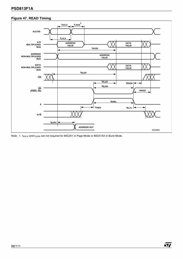
PSD813F1A
88/111
Figure 47. READ Timing
Note: 1. tAVLX and tLXAX are not required for 80C251 in Page Mode or 80C51XA in Burst Mode.
tAVLX tLXAX1
tLVLX
tAVQV
tSLQV
tRLQV tRHQX
tRHQZ
tELTL
tEHEL
tRLRH
tTHEH
tAVPV
ADDRESSVALID
ADDRESSVALID
DATAVALID
DATAVALID
ADDRESS OUT
ALE/AS
A/DMULTIPLEXED
BUS
ADDRESSNON-MULTIPLEXED
BUS
DATANON-MULTIPLEXED
BUS
CSI
RD(PSEN, DS)
E
R/W
AI02895
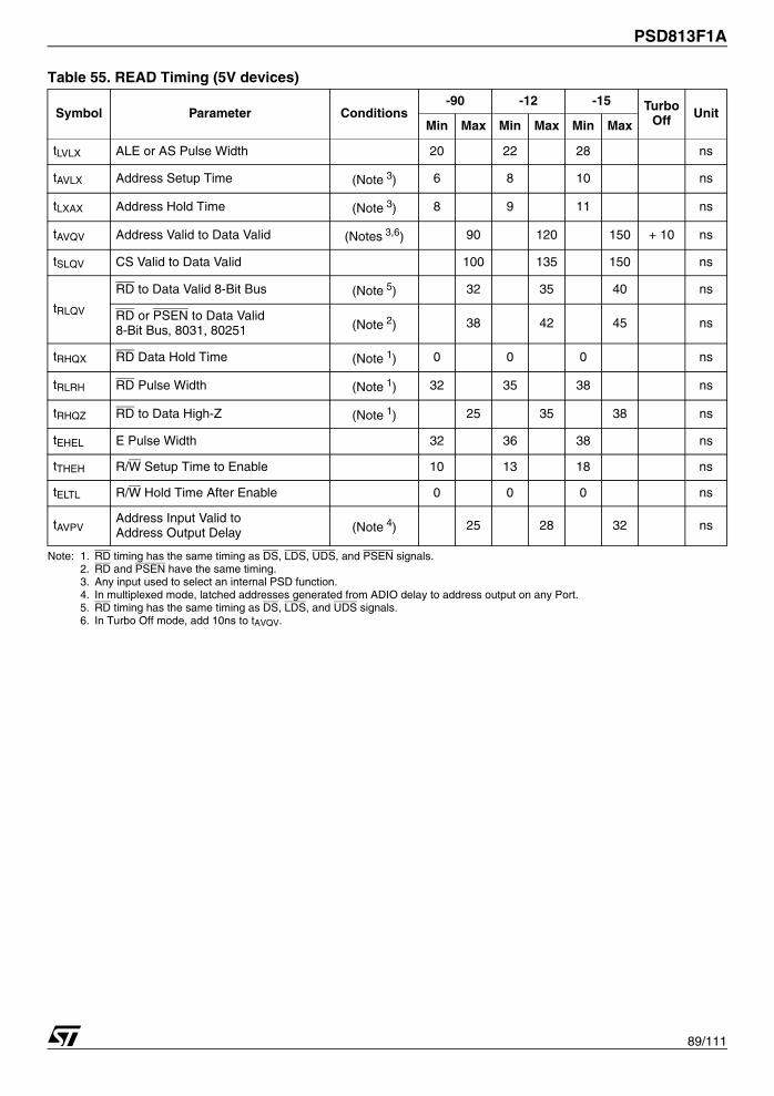
89/111
PSD813F1A
Table 55. READ Timing (5V devices)
Note: 1. RD timing has the same timing as DS, LDS, UDS, and PSEN signals.2. RD and PSEN have the same timing.3. Any input used to select an internal PSD function.4. In multiplexed mode, latched addresses generated from ADIO delay to address output on any Port.5. RD timing has the same timing as DS, LDS, and UDS signals.6. In Turbo Off mode, add 10ns to tAVQV.
Symbol Parameter Conditions-90 -12 -15 Turbo
Off UnitMin Max Min Max Min Max
tLVLX ALE or AS Pulse Width 20 22 28 ns
tAVLX Address Setup Time (Note 3) 6 8 10 ns
tLXAX Address Hold Time (Note 3) 8 9 11 ns
tAVQV Address Valid to Data Valid (Notes 3,6) 90 120 150 + 10 ns
tSLQV CS Valid to Data Valid 100 135 150 ns
tRLQV
RD to Data Valid 8-Bit Bus (Note 5) 32 35 40 ns
RD or PSEN to Data Valid 8-Bit Bus, 8031, 80251 (Note 2) 38 42 45 ns
tRHQX RD Data Hold Time (Note 1) 0 0 0 ns
tRLRH RD Pulse Width (Note 1) 32 35 38 ns
tRHQZ RD to Data High-Z (Note 1) 25 35 38 ns
tEHEL E Pulse Width 32 36 38 ns
tTHEH R/W Setup Time to Enable 10 13 18 ns
tELTL R/W Hold Time After Enable 0 0 0 ns
tAVPVAddress Input Valid toAddress Output Delay (Note 4) 25 28 32 ns
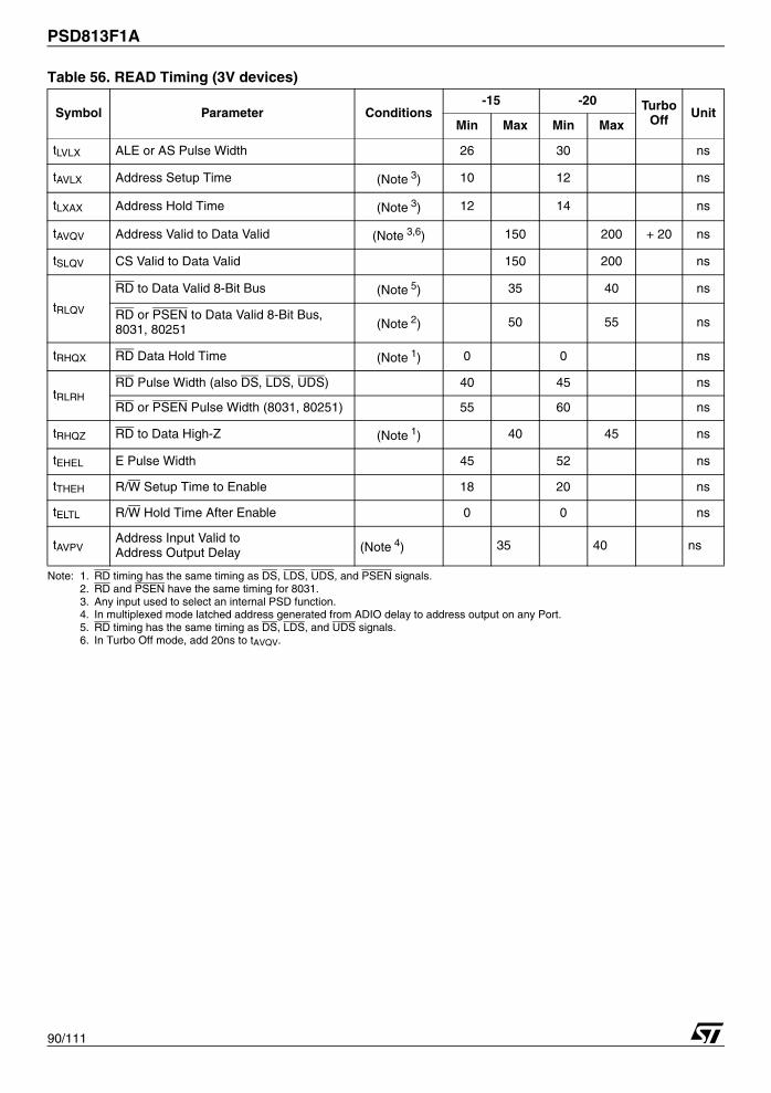
PSD813F1A
90/111
Table 56. READ Timing (3V devices)
Note: 1. RD timing has the same timing as DS, LDS, UDS, and PSEN signals.2. RD and PSEN have the same timing for 8031.3. Any input used to select an internal PSD function.4. In multiplexed mode latched address generated from ADIO delay to address output on any Port.5. RD timing has the same timing as DS, LDS, and UDS signals.6. In Turbo Off mode, add 20ns to tAVQV.
Symbol Parameter Conditions-15 -20 Turbo
Off UnitMin Max Min Max
tLVLX ALE or AS Pulse Width 26 30 ns
tAVLX Address Setup Time (Note 3) 10 12 ns
tLXAX Address Hold Time (Note 3) 12 14 ns
tAVQV Address Valid to Data Valid (Note 3,6) 150 200 + 20 ns
tSLQV CS Valid to Data Valid 150 200 ns
tRLQV
RD to Data Valid 8-Bit Bus (Note 5) 35 40 ns
RD or PSEN to Data Valid 8-Bit Bus,8031, 80251 (Note 2) 50 55 ns
tRHQX RD Data Hold Time (Note 1) 0 0 ns
tRLRHRD Pulse Width (also DS, LDS, UDS) 40 45 ns
RD or PSEN Pulse Width (8031, 80251) 55 60 ns
tRHQZ RD to Data High-Z (Note 1) 40 45 ns
tEHEL E Pulse Width 45 52 ns
tTHEH R/W Setup Time to Enable 18 20 ns
tELTL R/W Hold Time After Enable 0 0 ns
tAVPVAddress Input Valid toAddress Output Delay (Note 4) 35 40 ns
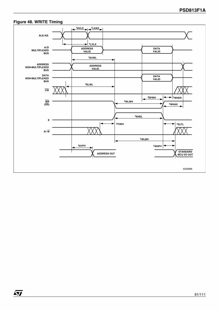
91/111
PSD813F1A
Figure 48. WRITE TimingtAVLX tLXAX
tLVLX
tAVWL
tSLWL
tWHDX
tWHAX
tELTL
tEHEL
tWLMV
tWLWH
tDVWH
tTHEH
tAVPV
ADDRESSVALID
ADDRESSVALID
DATAVALID
DATAVALID
ADDRESS OUT
tWHPV
STANDARDMCU I/O OUT
ALE/AS
A/DMULTIPLEXED
BUS
ADDRESSNON-MULTIPLEXED
BUS
DATANON-MULTIPLEXED
BUS
CSI
WR(DS)
E
R/ W
AI02896
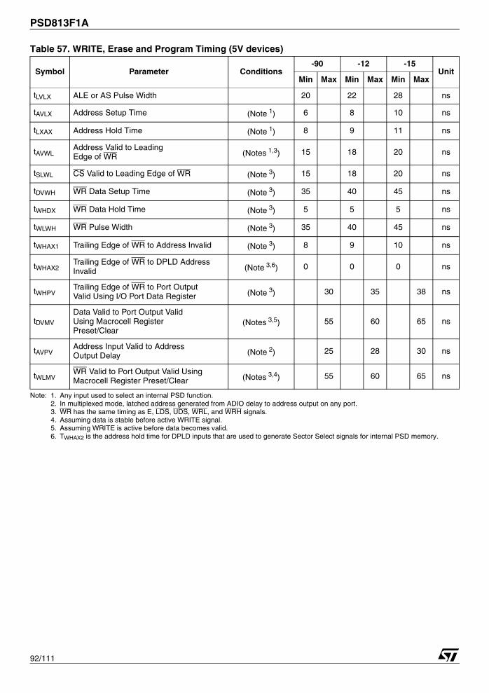
PSD813F1A
92/111
Table 57. WRITE, Erase and Program Timing (5V devices)
Note: 1. Any input used to select an internal PSD function.2. In multiplexed mode, latched address generated from ADIO delay to address output on any port.3. WR has the same timing as E, LDS, UDS, WRL, and WRH signals.4. Assuming data is stable before active WRITE signal.5. Assuming WRITE is active before data becomes valid.6. TWHAX2 is the address hold time for DPLD inputs that are used to generate Sector Select signals for internal PSD memory.
Symbol Parameter Conditions-90 -12 -15
UnitMin Max Min Max Min Max
tLVLX ALE or AS Pulse Width 20 22 28 ns
tAVLX Address Setup Time (Note 1) 6 8 10 ns
tLXAX Address Hold Time (Note 1) 8 9 11 ns
tAVWLAddress Valid to LeadingEdge of WR (Notes 1,3) 15 18 20 ns
tSLWL CS Valid to Leading Edge of WR (Note 3) 15 18 20 ns
tDVWH WR Data Setup Time (Note 3) 35 40 45 ns
tWHDX WR Data Hold Time (Note 3) 5 5 5 ns
tWLWH WR Pulse Width (Note 3) 35 40 45 ns
tWHAX1 Trailing Edge of WR to Address Invalid (Note 3) 8 9 10 ns
tWHAX2Trailing Edge of WR to DPLD Address Invalid (Note 3,6) 0 0 0 ns
tWHPVTrailing Edge of WR to Port OutputValid Using I/O Port Data Register (Note 3) 30 35 38 ns
tDVMV
Data Valid to Port Output ValidUsing Macrocell Register Preset/Clear
(Notes 3,5) 55 60 65 ns
tAVPVAddress Input Valid to AddressOutput Delay (Note 2) 25 28 30 ns
tWLMVWR Valid to Port Output Valid UsingMacrocell Register Preset/Clear (Notes 3,4) 55 60 65 ns

93/111
PSD813F1A
Table 58. WRITE Timing (3V devices)
Note: 1. Any input used to select an internal PSD function.2. In multiplexed mode, latched address generated from ADIO delay to address output on any port.3. WR has the same timing as E, LDS, UDS, WRL, and WRH signals.4. Assuming data is stable before active WRITE signal.5. Assuming WRITE is active before data becomes valid.6. TWHAX2 is the address hold time for DPLD inputs that are used to generate Sector Select signals for internal PSD memory.
Table 59. Flash Program, WRITE and Erase Times (5V devices)
Note: 1. Programmed to all zero before erase.2. The polling status, DQ7, is valid tQ7VQV time units before the data byte, DQ0-DQ7, is valid for reading.
Symbol Parameter Conditions-15 -20
UnitMin Max Min Max
tLVLX ALE or AS Pulse Width 26 30
tAVLX Address Setup Time (Note 1) 10 12 ns
tLXAX Address Hold Time (Note 1) 12 14 ns
tAVWLAddress Valid to LeadingEdge of WR (Notes 1,3) 20 25 ns
tSLWL CS Valid to Leading Edge of WR (Note 3) 20 25 ns
tDVWH WR Data Setup Time (Note 3) 45 50 ns
tWHDX WR Data Hold Time (Note 3) 8 10 ns
tWLWH WR Pulse Width (Note 3) 48 53 ns
tWHAX1 Trailing Edge of WR to Address Invalid (Note 3) 12 17 ns
tWHAX2 Trailing Edge of WR to DPLD Address Invalid (Note 3,6) 0 0 ns
tWHPVTrailing Edge of WR to Port OutputValid Using I/O Port Data Register (Note 3) 45 50 ns
tDVMVData Valid to Port Output ValidUsing Macrocell Register Preset/Clear (Notes 3,5) 90 100 ns
tAVPVAddress Input Valid to AddressOutput Delay (Note 2) 48 55 ns
tWLMVWR Valid to Port Output Valid UsingMacrocell Register Preset/Clear (Notes 3,4) 90 100 ns
Symbol Parameter Min. Typ. Max. Unit
Flash Program 8.5 s
Flash Bulk Erase1 (pre-programmed) 3 30 s
Flash Bulk Erase (not pre-programmed) 10 s
tWHQV3 Sector Erase (pre-programmed) 1 30 s
tWHQV2 Sector Erase (not pre-programmed) 2.2 s
tWHQV1 Byte Program 14 1200 µs
Program / Erase Cycles (per Sector) 100,000 cycles
tWHWLO Sector Erase Time-Out 100 µs
tQ7VQV DQ7 Valid to Output (DQ7-DQ0) Valid (Data Polling)2 30 ns
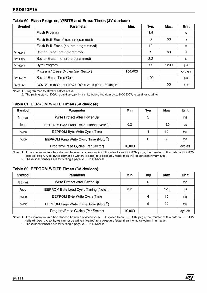
PSD813F1A
94/111
Table 60. Flash Program, WRITE and Erase Times (3V devices)
Note: 1. Programmed to all zero before erase.2. The polling status, DQ7, is valid tQ7VQV time units before the data byte, DQ0-DQ7, is valid for reading.
Table 61. EEPROM WRITE Times (5V devices)
Note: 1. If the maximum time has elapsed between successive WRITE cycles to an EEPROM page, the transfer of this data to EEPROMcells will begin. Also, bytes cannot be written (loaded) to a page any faster than the indicated minimum type.
2. These specifications are for writing a page to EEPROM cells.
Table 62. EEPROM WRITE Times (3V devices)
Note: 1. If the maximum time has elapsed between successive WRITE cycles to an EEPROM page, the transfer of this data to EEPROMcells will begin. Also, bytes cannot be written (loaded) to a page any faster than the indicated minimum type.
2. These specifications are for writing a page to EEPROM cells.
Symbol Parameter Min. Typ. Max. Unit
Flash Program 8.5 s
Flash Bulk Erase1 (pre-programmed) 3 30 s
Flash Bulk Erase (not pre-programmed) 10 s
tWHQV3 Sector Erase (pre-programmed) 1 30 s
tWHQV2 Sector Erase (not pre-programmed) 2.2 s
tWHQV1 Byte Program 14 1200 µs
Program / Erase Cycles (per Sector) 100,000 cycles
tWHWLO Sector Erase Time-Out 100 µs
tQ7VQV DQ7 Valid to Output (DQ7-DQ0) Valid (Data Polling)2 30 ns
Symbol Parameter Min Typ Max Unit
tEEHWL Write Protect After Power Up 5 ms
tBLC EEPROM Byte Load Cycle Timing (Note 1) 0.2 120 µs
tWCB EEPROM Byte Write Cycle Time 4 10 ms
tWCP EEPROM Page Write Cycle Time (Note 2) 6 30 ms
Program/Erase Cycles (Per Sector) 10,000 cycles
Symbol Parameter Min Typ Max Unit
tEEHWL Write Protect After Power Up 5 ms
tBLC EEPROM Byte Load Cycle Timing (Note 1) 0.2 120 µs
tWCB EEPROM Byte Write Cycle Time 4 10 ms
tWCP EEPROM Page Write Cycle Time (Note 2) 6 30 ms
Program/Erase Cycles (Per Sector) 10,000 cycles
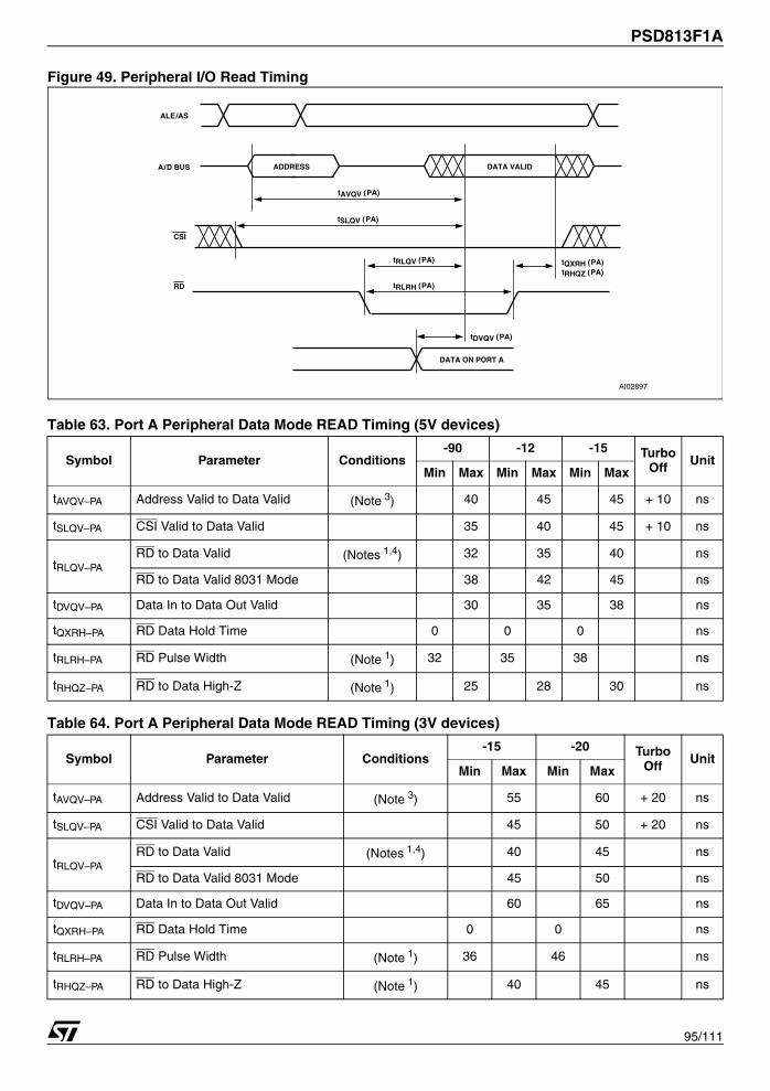
95/111
PSD813F1A
Figure 49. Peripheral I/O Read Timing
Table 63. Port A Peripheral Data Mode READ Timing (5V devices)
Table 64. Port A Peripheral Data Mode READ Timing (3V devices)
Symbol Parameter Conditions-90 -12 -15 Turbo
Off UnitMin Max Min Max Min Max
tAVQV–PA Address Valid to Data Valid (Note 3) 40 45 45 + 10 ns
tSLQV–PA CSI Valid to Data Valid 35 40 45 + 10 ns
tRLQV–PARD to Data Valid (Notes 1,4) 32 35 40 ns
RD to Data Valid 8031 Mode 38 42 45 ns
tDVQV–PA Data In to Data Out Valid 30 35 38 ns
tQXRH–PA RD Data Hold Time 0 0 0 ns
tRLRH–PA RD Pulse Width (Note 1) 32 35 38 ns
tRHQZ–PA RD to Data High-Z (Note 1) 25 28 30 ns
Symbol Parameter Conditions-15 -20 Turbo
Off UnitMin Max Min Max
tAVQV–PA Address Valid to Data Valid (Note 3) 55 60 + 20 ns
tSLQV–PA CSI Valid to Data Valid 45 50 + 20 ns
tRLQV–PARD to Data Valid (Notes 1,4) 40 45 ns
RD to Data Valid 8031 Mode 45 50 ns
tDVQV–PA Data In to Data Out Valid 60 65 ns
tQXRH–PA RD Data Hold Time 0 0 ns
tRLRH–PA RD Pulse Width (Note 1) 36 46 ns
tRHQZ–PA RD to Data High-Z (Note 1) 40 45 ns
tQXRH (PA)tRLQV (PA)
tRLRH (PA)
tDVQV (PA)
tRHQZ (PA)
tSLQV (PA)
tAVQV (PA)
ADDRESS DATA VALID
ALE/AS
A/D BUS
RD
DATA ON PORT A
CSI
AI02897

PSD813F1A
96/111
Figure 50. Peripheral I/O WRITE Timing
Table 65. Port A Peripheral Data Mode WRITE Timing (5V devices)
Note: 1. RD has the same timing as DS, LDS, UDS, and PSEN (in 8031 combined mode).2. WR has the same timing as the E, LDS, UDS, WRL, and WRH signals.3. Any input used to select Port A Data Peripheral mode.4. Data is already stable on Port A.5. Data stable on ADIO pins to data on Port A.
Table 66. Port A Peripheral Data Mode WRITE Timing (3V devices)
Note: 1. RD has the same timing as DS, LDS, UDS, and PSEN (in 8031 combined mode) signals.2. WR has the same timing as the E, LDS, UDS, WRL, and WRH signals.3. Any input used to select Port A Data Peripheral mode.4. Data is already stable on Port A.5. Data stable on ADIO pins to data on Port A.
Symbol Parameter Conditions-90 -12 -15
UnitMin Max Min Max Min Max
tWLQV–PA WR to Data Propagation Delay (Note 2) 35 38 40 ns
tDVQV–PA Data to Port A Data Propagation Delay (Note 5) 30 35 38 ns
tWHQZ–PA WR Invalid to Port A Tri-state (Note 2) 25 30 33 ns
Symbol Parameter Conditions-15 -20
UnitMin Max Min Max
tWLQV–PA WR to Data Propagation Delay (Note 2) 45 55 ns
tDVQV–PA Data to Port A Data Propagation Delay (Note 5) 40 45 ns
tWHQZ–PA WR Invalid to Port A Tri-state (Note 2) 33 35 ns
tDVQV (PA)
tWLQV (PA) tWHQZ (PA)
ADDRESS DATA OUTA /D BUS
WR
PORT ADATA OUT
ALE/AS
AI02898
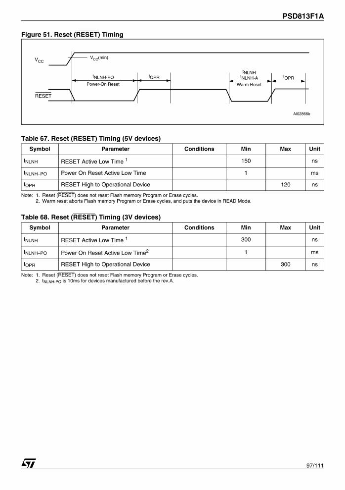
97/111
PSD813F1A
Figure 51. Reset (RESET) Timing
Table 67. Reset (RESET) Timing (5V devices)
Note: 1. Reset (RESET) does not reset Flash memory Program or Erase cycles.2. Warm reset aborts Flash memory Program or Erase cycles, and puts the device in READ Mode.
Table 68. Reset (RESET) Timing (3V devices)
Note: 1. Reset (RESET) does not reset Flash memory Program or Erase cycles.2. tNLNH-PO is 10ms for devices manufactured before the rev.A.
Symbol Parameter Conditions Min Max Unit
tNLNH RESET Active Low Time 1 150 ns
tNLNH–PO Power On Reset Active Low Time 1 ms
tOPR RESET High to Operational Device 120 ns
Symbol Parameter Conditions Min Max Unit
tNLNH RESET Active Low Time 1 300 ns
tNLNH–PO Power On Reset Active Low Time2 1 ms
tOPR RESET High to Operational Device 300 ns
tNLNH-PO tOPR
AI02866b
RESET
tNLNHtNLNH-A tOPR
VCCVCC(min)
Power-On Reset Warm Reset
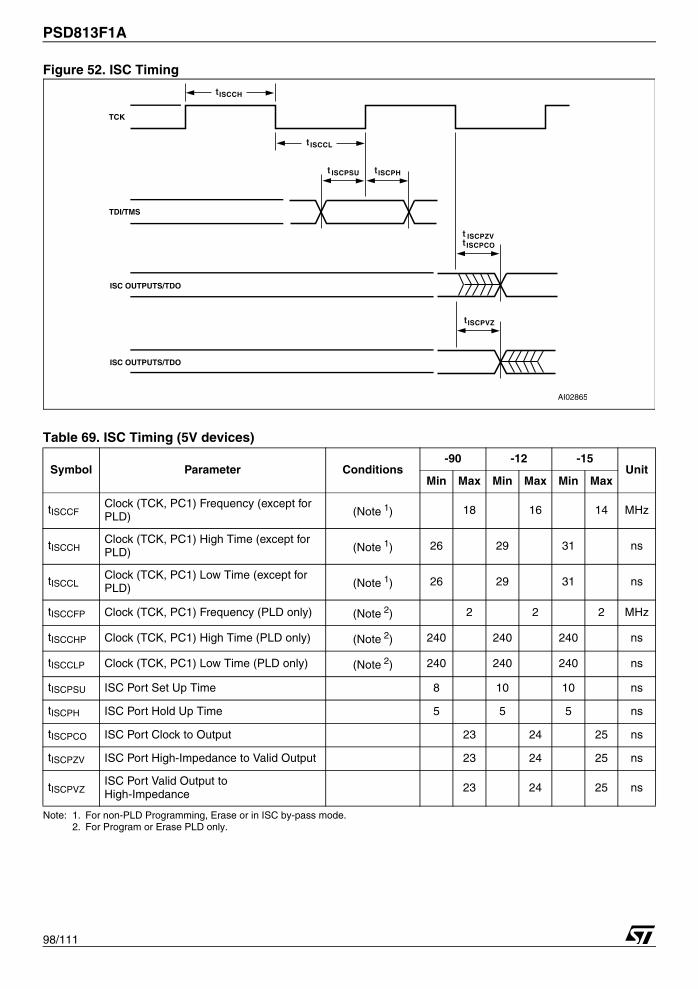
PSD813F1A
98/111
Figure 52. ISC Timing
Table 69. ISC Timing (5V devices)
Note: 1. For non-PLD Programming, Erase or in ISC by-pass mode.2. For Program or Erase PLD only.
Symbol Parameter Conditions-90 -12 -15
UnitMin Max Min Max Min Max
tISCCFClock (TCK, PC1) Frequency (except for PLD) (Note 1) 18 16 14 MHz
tISCCHClock (TCK, PC1) High Time (except for PLD) (Note 1) 26 29 31 ns
tISCCLClock (TCK, PC1) Low Time (except for PLD) (Note 1) 26 29 31 ns
tISCCFP Clock (TCK, PC1) Frequency (PLD only) (Note 2) 2 2 2 MHz
tISCCHP Clock (TCK, PC1) High Time (PLD only) (Note 2) 240 240 240 ns
tISCCLP Clock (TCK, PC1) Low Time (PLD only) (Note 2) 240 240 240 ns
tISCPSU ISC Port Set Up Time 8 10 10 ns
tISCPH ISC Port Hold Up Time 5 5 5 ns
tISCPCO ISC Port Clock to Output 23 24 25 ns
tISCPZV ISC Port High-Impedance to Valid Output 23 24 25 ns
tISCPVZISC Port Valid Output to High-Impedance 23 24 25 ns
ISCCH
TCK
TDI/TMS
ISC OUTPUTS/TDO
ISC OUTPUTS/TDO
t
ISCCLt
ISCPHtISCPSUt
ISCPVZt
ISCPZVtISCPCOt
AI02865
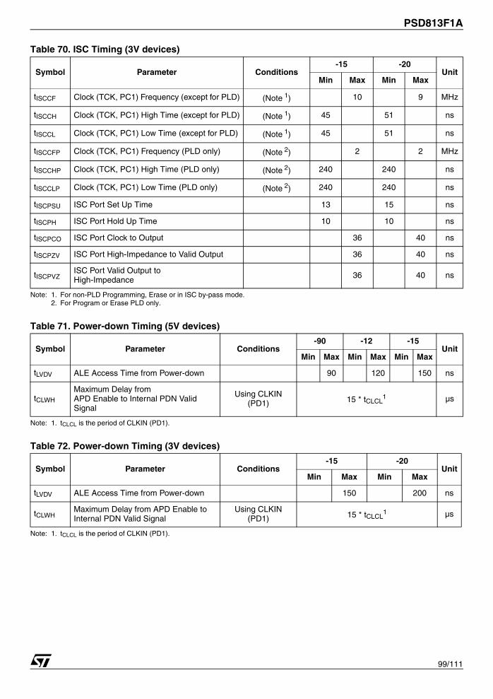
99/111
PSD813F1A
Table 70. ISC Timing (3V devices)
Note: 1. For non-PLD Programming, Erase or in ISC by-pass mode.2. For Program or Erase PLD only.
Table 71. Power-down Timing (5V devices)
Note: 1. tCLCL is the period of CLKIN (PD1).
Table 72. Power-down Timing (3V devices)
Note: 1. tCLCL is the period of CLKIN (PD1).
Symbol Parameter Conditions-15 -20
UnitMin Max Min Max
tISCCF Clock (TCK, PC1) Frequency (except for PLD) (Note 1) 10 9 MHz
tISCCH Clock (TCK, PC1) High Time (except for PLD) (Note 1) 45 51 ns
tISCCL Clock (TCK, PC1) Low Time (except for PLD) (Note 1) 45 51 ns
tISCCFP Clock (TCK, PC1) Frequency (PLD only) (Note 2) 2 2 MHz
tISCCHP Clock (TCK, PC1) High Time (PLD only) (Note 2) 240 240 ns
tISCCLP Clock (TCK, PC1) Low Time (PLD only) (Note 2) 240 240 ns
tISCPSU ISC Port Set Up Time 13 15 ns
tISCPH ISC Port Hold Up Time 10 10 ns
tISCPCO ISC Port Clock to Output 36 40 ns
tISCPZV ISC Port High-Impedance to Valid Output 36 40 ns
tISCPVZISC Port Valid Output to High-Impedance 36 40 ns
Symbol Parameter Conditions-90 -12 -15
UnitMin Max Min Max Min Max
tLVDV ALE Access Time from Power-down 90 120 150 ns
tCLWH
Maximum Delay from APD Enable to Internal PDN Valid Signal
Using CLKIN (PD1) 15 * tCLCL
1 µs
Symbol Parameter Conditions-15 -20
UnitMin Max Min Max
tLVDV ALE Access Time from Power-down 150 200 ns
tCLWHMaximum Delay from APD Enable to Internal PDN Valid Signal
Using CLKIN (PD1) 15 * tCLCL
1 µs
PSD813F1A
100/111
PACKAGE MECHANICALIn order to meet environmental requirements, SToffers these devices in ECOPACK® packages.These packages have a Lead-free second level in-terconnect. The category of second level intercon-nect is marked on the package and on the inner
box label, in compliance with JEDEC StandardJESD97. The maximum ratings related to soldering condi-tions are also marked on the inner box label. ECOPACK is an ST trademark. ECOPACK speci-fications are available at: www.st.com.
Figure 53. PQFP52 - 52-pin Plastic, Quad, Flat Package Mechanical Drawing
Note: Drawing is not to scale.
QFP-A
Nd
E1
CP
b
e
A2
A
N
LA1 α
D1
D
1
ENe
c
D2
E2
L1

101/111
PSD813F1A
Table 73. PQFP52 - 52-pin Plastic, Quad, Flat Package Mechanical Dimensions
Symb.mm inches
Typ. Min. Max. Typ. Min. Max.
A 2.35 0.093
A1 0.25 0.010
A2 2.00 1.80 2.10 0.079 0.077 0.083
b 0.22 0.38 0.009 0.015
c 0.11 0.23 0.004 0.009
D 13.20 13.15 13.25 0.520 0.518 0.522
D1 10.00 9.95 10.05 0.394 0.392 0.396
D2 7.80 – – 0.307 – –
E 13.20 13.15 13.25 0.520 0.518 0.522
E1 10.00 9.95 10.05 0.394 0.392 0.396
E2 7.80 – – 0.307 – –
e 0.65 – – 0.026
L 0.88 0.73 1.03 0.035 0.029 0.041
L1 1.60 – – 0.063
α 0° 7° 0° 7°
N 52 52
Nd 13 13
Ne 13 13
CP 0.10 0.004
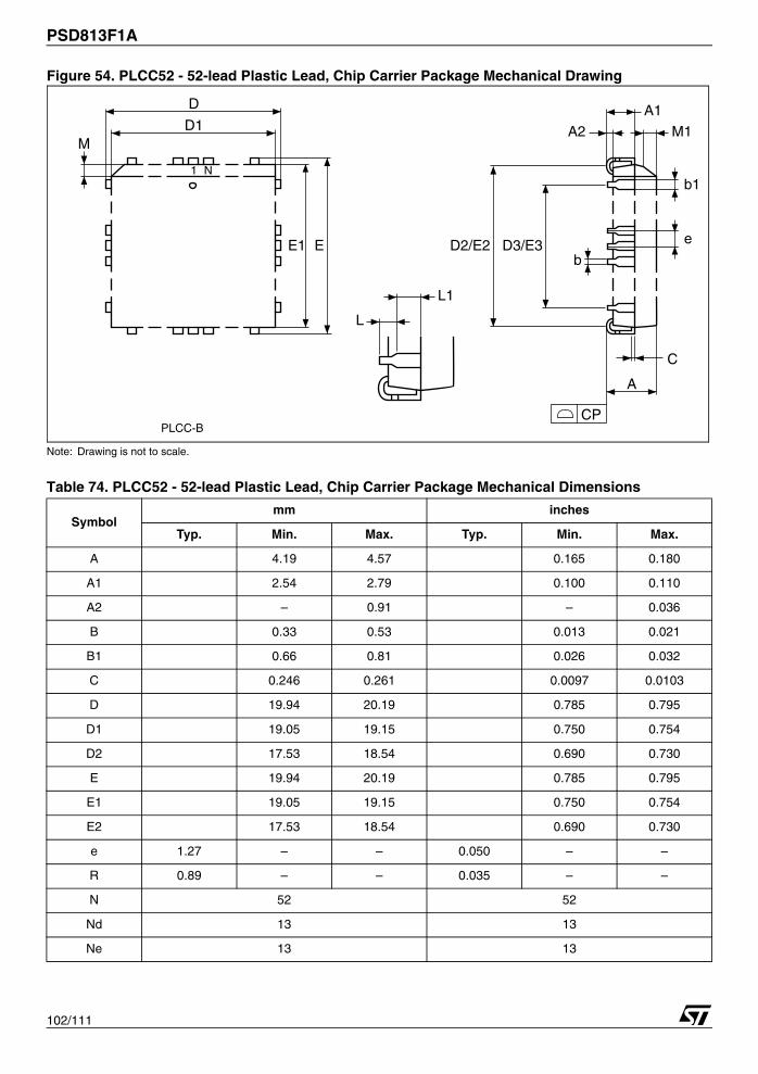
PSD813F1A
102/111
Figure 54. PLCC52 - 52-lead Plastic Lead, Chip Carrier Package Mechanical Drawing
Note: Drawing is not to scale.
Table 74. PLCC52 - 52-lead Plastic Lead, Chip Carrier Package Mechanical Dimensions
Symbolmm inches
Typ. Min. Max. Typ. Min. Max.
A 4.19 4.57 0.165 0.180
A1 2.54 2.79 0.100 0.110
A2 – 0.91 – 0.036
B 0.33 0.53 0.013 0.021
B1 0.66 0.81 0.026 0.032
C 0.246 0.261 0.0097 0.0103
D 19.94 20.19 0.785 0.795
D1 19.05 19.15 0.750 0.754
D2 17.53 18.54 0.690 0.730
E 19.94 20.19 0.785 0.795
E1 19.05 19.15 0.750 0.754
E2 17.53 18.54 0.690 0.730
e 1.27 – – 0.050 – –
R 0.89 – – 0.035 – –
N 52 52
Nd 13 13
Ne 13 13
PLCC-B
D
E1 E
1 N
D1
CP
bD2/E2 e
b1
A1
A
A2
D3/E3
M
L1
L
C
M1
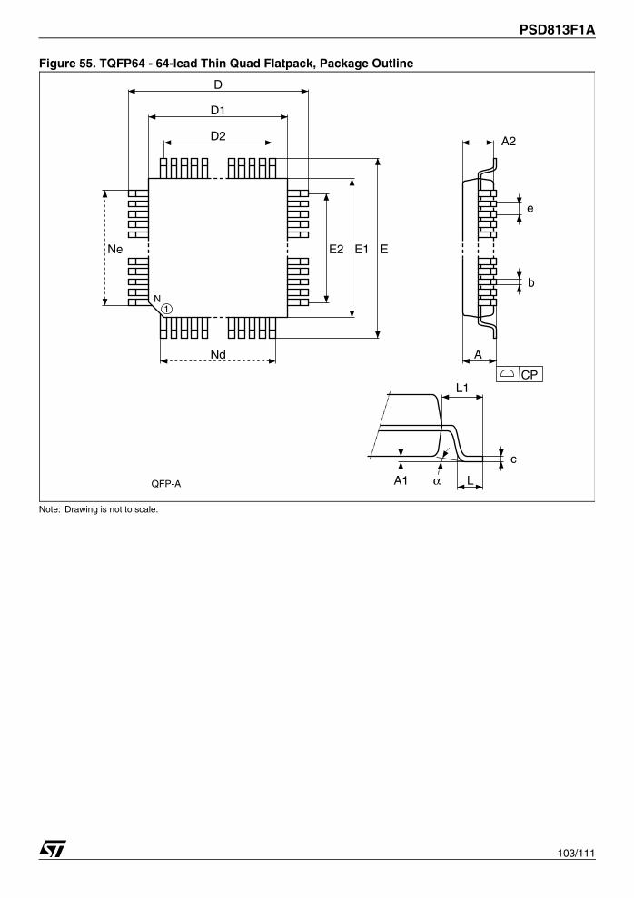
103/111
PSD813F1A
Figure 55. TQFP64 - 64-lead Thin Quad Flatpack, Package Outline
Note: Drawing is not to scale.
QFP-A
Nd
E1
CP
b
e
A2
A
N
LA1 α
D1
D
1
ENe
c
D2
E2
L1
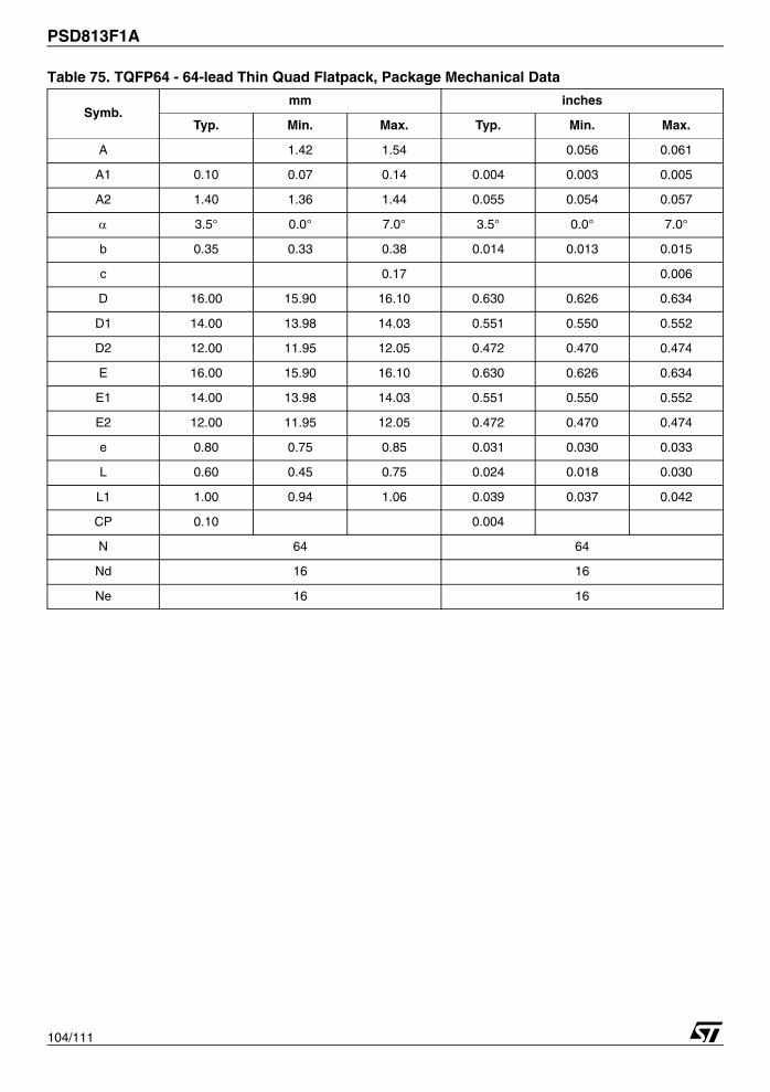
PSD813F1A
104/111
Table 75. TQFP64 - 64-lead Thin Quad Flatpack, Package Mechanical Data
Symb.mm inches
Typ. Min. Max. Typ. Min. Max.
A 1.42 1.54 0.056 0.061
A1 0.10 0.07 0.14 0.004 0.003 0.005
A2 1.40 1.36 1.44 0.055 0.054 0.057
α 3.5° 0.0° 7.0° 3.5° 0.0° 7.0°
b 0.35 0.33 0.38 0.014 0.013 0.015
c 0.17 0.006
D 16.00 15.90 16.10 0.630 0.626 0.634
D1 14.00 13.98 14.03 0.551 0.550 0.552
D2 12.00 11.95 12.05 0.472 0.470 0.474
E 16.00 15.90 16.10 0.630 0.626 0.634
E1 14.00 13.98 14.03 0.551 0.550 0.552
E2 12.00 11.95 12.05 0.472 0.470 0.474
e 0.80 0.75 0.85 0.031 0.030 0.033
L 0.60 0.45 0.75 0.024 0.018 0.030
L1 1.00 0.94 1.06 0.039 0.037 0.042
CP 0.10 0.004
N 64 64
Nd 16 16
Ne 16 16
105/111
PSD813F1A
PART NUMBERING
Table 76. Ordering Information Scheme
Example: PSD8 1 3 F 1 A – 15 J 1 T
Device Type
PSD8 = 8-bit PSD with Register Logic
SRAM Capacity
1 = 16 Kbit
Flash Memory Capacity
3 = 1 Mbit (128Kb x 8)
2nd Flash Memory
1 = 256 Kbit EEPROM
Operating Voltage
blank = VCC = 4.5 to 5.5V
Speed
70 = 70ns
90 = 90ns
12 = 120ns
15 = 150ns
Package
J = ECOPACK PLCC52
M = ECOPACK PQFP52
U = ECOPACK TQFP64
Temperature Range
blank = 0 to 70°C (commercial)
1 = –40 to 85°C (industrial)
Option
T = Tape & Reel Packing
PSD813F1A
106/111
For other options, or for more information on any aspect of this device, please contact the ST Sales Officenearest you.

107/111
PSD813F1A
APPENDIX A. PQFP52 PIN ASSIGNMENTS
Table 77. PQFP52 Connections (Figure 2)
Pin Number Pin Assignments
1 PD2
2 PD1
3 PD0
4 PC7
5 PC6
6 PC5
7 PC4
8 VCC
9 GND
10 PC3
11 PC2
12 PC1
13 PC0
14 PA7
15 PA6
16 PA5
17 PA4
18 PA3
19 GND
20 PA2
21 PA1
22 PA0
23 AD0
24 AD1
25 AD2
26 AD3
Pin Number Pin Assignments
27 AD4
28 AD5
29 AD6
30 AD7
31 VCC
32 AD8
33 AD9
34 AD10
35 AD11
36 AD12
37 AD13
38 AD14
39 AD15
40 CNTL0
41 RESET
42 CNTL2
43 CNTL1
44 PB7
45 PB6
46 GND
47 PB5
48 PB4
49 PB3
50 PB2
51 PB1
52 PB0
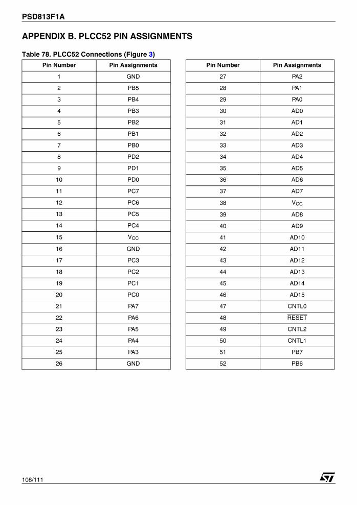
PSD813F1A
108/111
APPENDIX B. PLCC52 PIN ASSIGNMENTS
Table 78. PLCC52 Connections (Figure 3)
Pin Number Pin Assignments
1 GND
2 PB5
3 PB4
4 PB3
5 PB2
6 PB1
7 PB0
8 PD2
9 PD1
10 PD0
11 PC7
12 PC6
13 PC5
14 PC4
15 VCC
16 GND
17 PC3
18 PC2
19 PC1
20 PC0
21 PA7
22 PA6
23 PA5
24 PA4
25 PA3
26 GND
Pin Number Pin Assignments
27 PA2
28 PA1
29 PA0
30 AD0
31 AD1
32 AD2
33 AD3
34 AD4
35 AD5
36 AD6
37 AD7
38 VCC
39 AD8
40 AD9
41 AD10
42 AD11
43 AD12
44 AD13
45 AD14
46 AD15
47 CNTL0
48 RESET
49 CNTL2
50 CNTL1
51 PB7
52 PB6
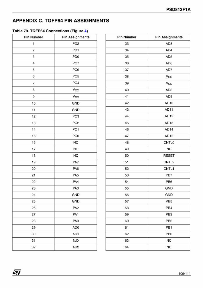
109/111
PSD813F1A
APPENDIX C. TQFP64 PIN ASSIGNMENTS
Table 79. TQFP64 Connections (Figure 4)
Pin Number Pin Assignments
1 PD2
2 PD1
3 PD0
4 PC7
5 PC6
6 PC5
7 PC4
8 VCC
9 VCC
10 GND
11 GND
12 PC3
13 PC2
14 PC1
15 PC0
16 NC
17 NC
18 NC
19 PA7
20 PA6
21 PA5
22 PA4
23 PA3
24 GND
25 GND
26 PA2
27 PA1
28 PA0
29 AD0
30 AD1
31 N/D
32 AD2
Pin Number Pin Assignments
33 AD3
34 AD4
35 AD5
36 AD6
37 AD7
38 VCC
39 VCC
40 AD8
41 AD9
42 AD10
43 AD11
44 AD12
45 AD13
46 AD14
47 AD15
48 CNTL0
49 NC
50 RESET
51 CNTL2
52 CNTL1
53 PB7
54 PB6
55 GND
56 GND
57 PB5
58 PB4
59 PB3
60 PB2
61 PB1
62 PB0
63 NC
64 NC
PSD813F1A
110/111
REVISION HISTORY
Table 80. Document Revision History
Date Rev. Description of Revision
August-2000 1.0 Document written in WSI format.
04-Jan-03 1.1Front page, and back two pages, in ST format, added to the PDF file. References to Waferscale, WSI, EasyFLASH and PSDsoft 2000 updated to ST, ST, Flash+PSD and PSDsoft Express.
06-Dec-03 2.0 Document converted to ST format. Package references corrected (Figure 1).
03-Jun-04 3.0 Document reformatted for DMS; Ordering Information corrected (Table 76); added TQFP64 package (Figure 1, 55; Table 75)
04-Aug-04 4.0 Correct connection, assignment (Figure 4; Table 79)
02-Oct-2008 5
Part number changed to PSD813F1A.Added ECOPACK text in cover page and in section PACKAGE MECHANICAL, page 100.Updated datasheet status to “not for new design”.Backup battery feature removed: updated Features Summary, Table 1 (pins PC2 and PC4), Block Diagram figure, Memory section, SRAM section, Port C – Functionality and Structure section. Removed SRAM standby mode in POWER MANAGEMENT. Updated PC2 in Table 78. Removed VSTBY, ISTBY, VOH1, VDF, and IIDLE from Table 45 and Table 46. Removed VSTBYON timings tables. Added 15ns speed in Table 76 Ordering information scheme.Updated disclaimer text.
111/111
PSD813F1A
Please Read Carefully:
Information in this document is provided solely in connection with ST products. STMicroelectronics NV and its subsidiaries (“ST”) reserve theright to make changes, corrections, modifications or improvements, to this document, and the products and services described herein at anytime, without notice.All ST products are sold pursuant to ST’s terms and conditions of sale.Purchasers are solely responsible for the choice, selection and use of the ST products and services described herein, and ST assumes noliability whatsoever relating to the choice, selection or use of the ST products and services described herein.No license, express or implied, by estoppel or otherwise, to any intellectual property rights is granted under this document. If any part of thisdocument refers to any third party products or services it shall not be deemed a license grant by ST for the use of such third party productsor services, or any intellectual property contained therein or considered as a warranty covering the use in any manner whatsoever of suchthird party products or services or any intellectual property contained therein.
UNLESS OTHERWISE SET FORTH IN ST’S TERMS AND CONDITIONS OF SALE ST DISCLAIMS ANY EXPRESS OR IMPLIEDWARRANTY WITH RESPECT TO THE USE AND/OR SALE OF ST PRODUCTS INCLUDING WITHOUT LIMITATION IMPLIEDWARRANTIES OF MERCHANTABILITY, FITNESS FOR A PARTICULAR PURPOSE (AND THEIR EQUIVALENTS UNDER THE LAWSOF ANY JURISDICTION), OR INFRINGEMENT OF ANY PATENT, COPYRIGHT OR OTHER INTELLECTUAL PROPERTY RIGHT.UNLESS EXPRESSLY APPROVED IN WRITING BY AN AUTHORIZED ST REPRESENTATIVE, ST PRODUCTS ARE NOTRECOMMENDED, AUTHORIZED OR WARRANTED FOR USE IN MILITARY, AIR CRAFT, SPACE, LIFE SAVING, OR LIFESUSTAINING APPLICATIONS, NOR IN PRODUCTS OR SYSTEMS WHERE FAILURE OR MALFUNCTION MAY RESULT INPERSONAL INJURY, DEATH, OR SEVERE PROPERTY OR ENVIRONMENTAL DAMAGE. ST PRODUCTS WHICH ARE NOTSPECIFIED AS "AUTOMOTIVE GRADE" MAY ONLY BE USED IN AUTOMOTIVE APPLICATIONS AT USER’S OWN RISK.
Resale of ST products with provisions different from the statements and/or technical features set forth in this document shall immediately voidany warranty granted by ST for the ST product or service described herein and shall not create or extend in any manner whatsoever, anyliability of ST.
ST and the ST logo are trademarks or registered trademarks of ST in various countries.
Information in this document supersedes and replaces all information previously supplied.
The ST logo is a registered trademark of STMicroelectronics. All other names are the property of their respective owners.
© 2008 STMicroelectronics - All rights reserved
STMicroelectronics group of companiesAustralia - Belgium - Brazil - Canada - China - Czech Republic - Finland - France - Germany - Hong Kong - India - Israel - Italy - Japan -
Malaysia - Malta - Morocco - Singapore - Spain - Sweden - Switzerland - United Kingdom - United States of Americawww.st.com