first-principles electronic transport...
TRANSCRIPT

• Electronic transport in nano-scale materials:
• Experiments
• Nonequilibrium Green function method
• Applications
From a scattering problem
Keldysh method
Taisuke Ozaki (ISSP, Univ. of Tokyo)
The Winter School on DFT: Theories and Practical Aspects, Dec. 19-23, CAS.
First-principles electronic transport calculations

Quantum conductance in gold nanowires
Takayanagi et al., Nature 395, 780 (1998).
After contacting two gold structures, gradually the two strucutres are pulled
along the axial direction. Then, the bridging region becomes gradually thinner.
Along with the structural change, the conductance changes stepwise.

(LaMnO3)2n/(SrMnO3)n superlattice
Bhattacharya et al., PRL 100, 257203 (2008)
Depending on the number of layers, the system exhibits a metal-
insulator transition. n<3 metal, 3≦n insulator
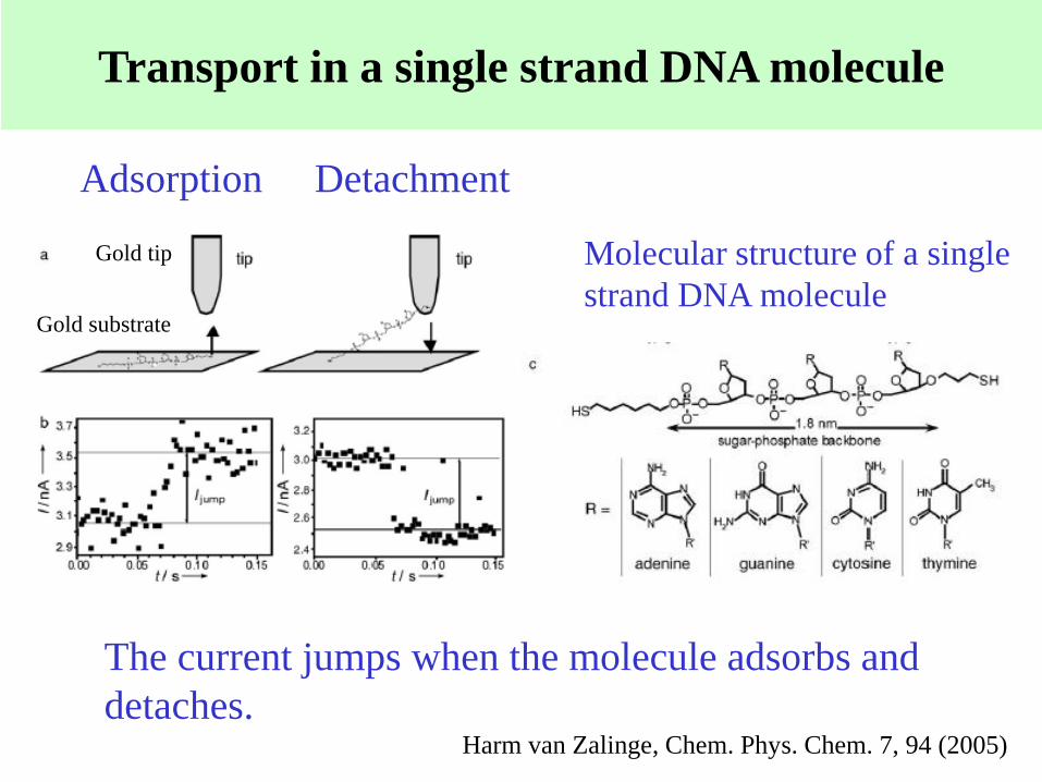
Transport in a single strand DNA molecule
Adsorption Detachment
Molecular structure of a single
strand DNA molecule
The current jumps when the molecule adsorbs and
detaches. Harm van Zalinge, Chem. Phys. Chem. 7, 94 (2005)
Gold tip
Gold substrate

A MgO
AFM
Fe
Fe
Application of tunneling magnet resistance (TMR) effect
A device used for a hard disk head is based on a tunneling magnet
resistance (TMR) effect, in which the tunneling current strongly
depends on the relative spin direction of two ferromagnetic regions.
Large current

A MgO
AFM
Fe
Fe
Application of tunneling magnet resistance (TMR) effect
A device used for a hard disk head is based on a tunneling magnet
resistance (TMR) effect, in which the tunneling current strongly
depends on the relative spin direction of two ferromagnetic regions.
Small current
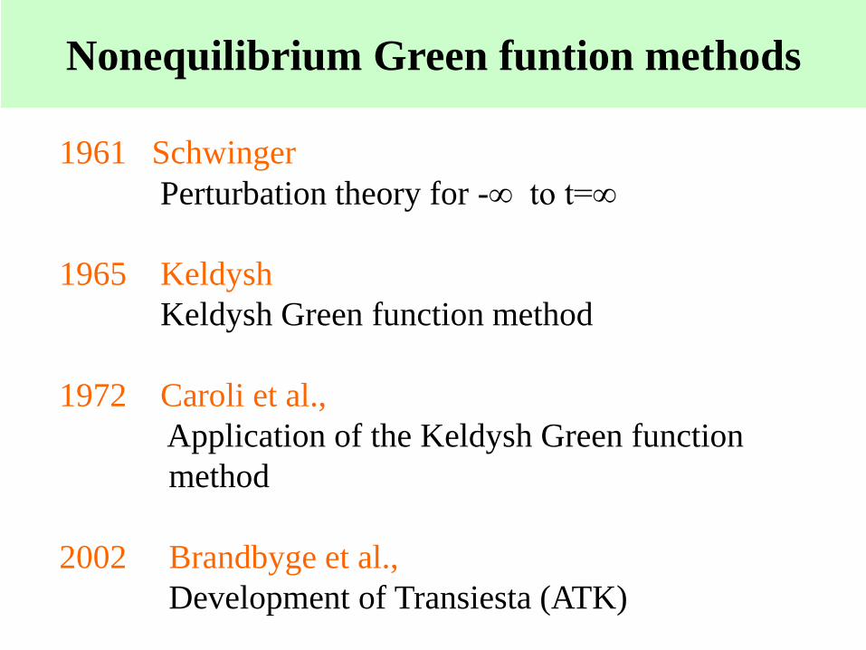
Nonequilibrium Green funtion methods
1961 Schwinger
Perturbation theory for -∞ to t=∞
1965 Keldysh
Keldysh Green function method
1972 Caroli et al.,
Application of the Keldysh Green function
method
2002 Brandbyge et al.,
Development of Transiesta (ATK)

Potential advantages of the NEGF method
1. The source and drain contacts are treated based on the same
theoretical framework as for the scattering region.
2. The electronic structure of the scattering region under a finite
source-drain bias voltage is self-consistently determined by
combining with first principle electronic structure calculation
methods such as the density functional theory (DFT) and the
Hartree-Fock (HF) method.
3. Many body effects in the transport properties, e.g., electron-
phonon
4. Its applicability to large-scale systems can be anticipated,
since the NEGF method relies practically on the locality of
basis functions in real space, resulting in computations for
sparse matrices.

Derivation of the NEGF method
1. From a scattering problem
2. From Keldysh Green funtion
Within one-particle picture, both the methods
give the same framework.

System connected to two reservoirs with
different chemical potential
1. The left and right reservoirs are infinitely large and
in thermo-equilibrium with different chemical potential.
2. They are connected via a small central region.
3. The total system may be in a non-equilibrium steady state
that electrons flow steadily from the left to right.

One-dimensional scattering problem
x=0 x=a
V0
ε<V0(Tunnel effect)
The one-dimensional
scattering problem for a
potential wall (x=0 to a)
can be solved analytically.
V0 < εReflection
Transmittance

Generalization of scattering problem in a quasi 1D
Lead 1 Lead 2Device
(1) Assume that the wave
function of the isolated lead
is known.
(2) Assume that the whole wave
function of the total system can be
given by
(3) By putting the whole wave
function in the step2 into the
Schroedinger eq., we obtain the
following equations:
The whole wave function can be
written by φ.

Charge density in the device
The charge density of the device can be calculated by considering the
contribution produced with the incident wave function.
All the contributions are summed up with the Fermi function.
Adding the contributions from each lead yields
Depending on the chemical potential,
the contribution of each lead varies.

Flux of probability density (1)
In the nonequilibrium steady state, assuming that the probability density conserves, and we
evaluate the flux of the probability density using the time-dependent Schroedinger equation.
The time evolution of the integrated probability density is given by
Each term can be regarded as the contribution from each lead k.
Thus, we have
2

Flux of probability density (2)
Lead 1 Lead 2Device
i1 Flux from the lead 1 to the device →
i2 Flux from the lead 2 to the device ←
In other words, in the steady state the flux (i1) of the probability
density from the lead 1 to the device is equal to that (-i2) from the
device to the lead 2. Note that the sign of i2 is opposite to that of
i1 when they are seen as current.
where the sign of the flux of the probability density ik is taken so that the direction from the the lead
k to the device can be positive.

Current (1)
Ψd and Ψ2 can be written by the wave function of the isolated lead 1.
Then, the current from the leads 1 to 2 is given by

Current (2)
Considering all the states in the lead 1, we obtain the formula of current from
the leads 1 to 2 as follows:
Adding all the contributions from each lead yields the formula:
Transmission

Summary: from a scattering problem
Transmission
The whole wave function is written by the incident wave function:
The charge density in the device is given by the sum of the contributions from each lead.
Considering the flux of the probability density, the current is given by

Conductance and transmission

Conductance and transmission: continued

System we consider
Assume that the periodicity on the bc plane, and non-
periodicity along the a-axisThus, we can write the Bloch wave function
on the bc plane
And, the problem can be cast to a 1D problem.
where the Hamiltonian is given by a block tri-
diagonal form:
T. Ozaki et al., PRB 81, 035116 (2010).

Green function of the device region
Using the block form of matrices and the following identity:
we obtain
where the self energies are explicitly given by

Assumption in the implementation of the NEGF method
It is assumed that the states for mR< mL in the central part
is in the thermal equilibrium. Then, the charge density can
be calculated by
Thermal equilibrium
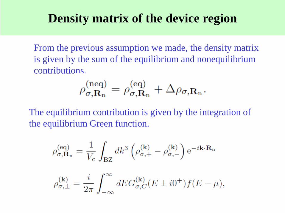
Density matrix of the device region
From the previous assumption we made, the density matrix
is given by the sum of the equilibrium and nonequilibrium
contributions.
The equilibrium contribution is given by the integration of
the equilibrium Green function.

Contour integration
By expressing the Fermi function
one can obtain a special distribution
of poles. The distribution gives
the extremely fast convergence.
T.Ozaki, PRB 75, 035123 (2007).

Nonequlibrium density matrix
Since NEGF is a non-analytic function, the integration is
performed on the real axis with a small imaginary part.

Poisson eq. with the boundary condition
Poisson eq.
FT for x-y plane
Discretization
Boundary conditions:
XY-FFT → linear eq. → XY-inverse FFT
Cost: O(Nxlog(Nx))×O(Nylog(Ny))×O(Nz)

Fe|MgO|Fe (TMR device)
Fe|MgO|Fe device has been gradually used as a hard disk head.

k-dependency of transmission (Fe|MgO|Fe)
up for↑↑ down for ↓↓
up for↑↓
mainly comes from s-orbital
mainly comes from d-orbital

LaMnO3/SrMnO3

Dual spin filter effect of the magnetic junction
up spin : flowing from right to left
down spin: flowing from left to right
→ Dual spin filter effect
Rectification ratio at 0.4V: 44.3
The same result is obtained for 6-ZGNR and 10-ZGNR.
PRB 81, 075422 (2010).

Conductance (transmission) of 8-ZGNR
For the up-spin
channel, the
conduction gap
disappears at -0.4
V, while the gap
keep increasing
for the down spin
channel.

Band structures with offset of 8-ZGNR
0 V
-0.4 V
-1.0 V
Blue shade: Conductance gap
for the up spin
Purple shade: Conductance gap
for the down spin
The energy regime where
the conductance gap
appears does correspond
to the energy region
where only the π and π*
states overlaps each other.

Wannier functions of π and π* states
Neither symmetric nor asymmetric
Symmetric
Asymmetric
calculated from by Marzari’s method

Wannier functions for π and π* states of 8-ZGNR
Wannier function of π
Wannier function of π *
Hopping integrals calculated by the Wannier functions
Since the π and π* states of 7-ZGNR are
neither symmetric nor asymmetric, the
corresponding hopping integrals survive.
Since for 8-ZGNR the π state is asymmetric and
the π* state is symmetric with respect to the σ
mirror plane, the hopping integrals are zero.
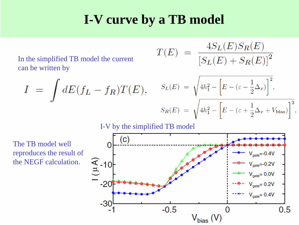
I-V curve by a TB model
In the simplified TB model the current
can be written by
I-V by the simplified TB model
The TB model well
reproduces the result of
the NEGF calculation.

Summary
The NEGF method combined with DFT provides a
general framework for a first-principles treatment
of electronic transport problems in a sense that
The method can be applicable to a wide variety of
materials including nanowires, superlattices,
molecular junctions, and carbon nanotubes.
• Equivalent treatment of lead and scattering region
• Self-consistent treatment under finite bias voltage
• Enabling large-scale calculations
• Inclusion of e-p and e-e interactions via self-energy terms