field engineering theory of operation
TRANSCRIPT

Field Engineering
Theory of Operation
Processing Unit
SY31-0207-1


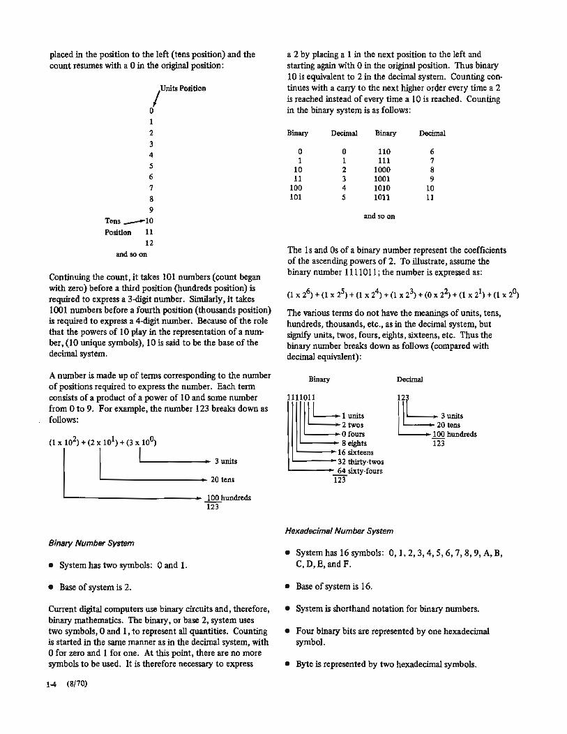


-TENS
Identifier (units)
UNITS
Identifier BitO Bit 1 Bit 2 Bit 3 Bit 4 Bit 5 Bit 6 Bit 7
Tens Reserved IndA Ind B Ind C IndO Ind E Ind F IndO
Units Reserved IndA Ind B Ind C Ind D Ind E Ind F IndO
Figure 6-7. Message Display Unit
Power On/Off Switch
This switch initiates the power on/off sequence of the system. A system reset is performed as part of the power on/off sequence. Main storage data may be lost when power is dropped.
Program Load Key
This key is pressed to start initial program loading from the MFCU or Disk file. The I/O device is selected with the program load selector switch. A system reset is performed as part of the program load sequence.
Pressing the program load key allows the first card or record from the MFCU or Disk File to be read and stored in main storage, beginning at location 0000. When the key is released, the CPU proceeds to execute the instruction sequence starting at location 0000. Normal program load from the MFCU is executed through the primary hopper.
Should the I/O device selected be not ready, the console I/O attention light will come on when the program load key is pressed. Normally, to complete the program load function, it is only necessary to ready the device.
Stop Key/Light
This key is pressed to cause a processor stop.
The processor is stopped at the end of the operation in progress when the key was pressed. I/O data transfers are completed without loss of information. Processor stop turns on the stop light.
The processor may be restarted without loss of information by depressing the start key.
Start Key
This key is pressed to start or continue operation.
Pressing the start key turns off the stop light and allows the processor to continue its normal operation.
The start key is also used, in conjunction with the CE modes of operation, to start and/or advance the processor clock.
On systems without the dual program feature, pressing the start key clears the message display unit and allows the program to proceed after a halt operation.
5410 FETOM (8/70) 6-7

Thermal Light
This light, along with the power check light, is turned on whenever an overtemperature condition is sensed in the CPU mainframe or electronic board in the printer. The light remains on until the condition is corrected and the power switch is turned to the off position. Overtemperature also results in power down. Normal power on can be performed after correcting the overtemperature condition. Figure 6-8 shows power check/thermal indications.
Lamp Test Switch
This switch turns on all system display lights.
Console Interrupt Key/Light (Dual Program Feature)
The console interrupt key is pressed to request immediate investigation of certain external conditions. The operation of the interrupt key is effective only when the interrupt light is on prior to pressing the key.
Pressing this key causes the normal operation to halt and to be replaced by an interrupt handling routine for interrupt level O. Normal operation will be resumed after the interrupt routine signals completion of interrupt servicing with the SIO instruction to reset interrupt request zero.
This light is on only when the system is being used in the dual program mode and interrupt level zero is enabled (console interrupt will be recognized).
Selection of whether the system is to be used in the dedicated or the dual program mode is accomplished with SIO instruction. The SIO instruction is also used to enable or disable the use of interrupt level zero.
Dual Program Control Switch
This rotary switch is normally used in conjunction with the console interrupt key. The status of this switch is sampled with a TIO instruction.
POWER CHECK/THERMAL INDICATIONS
INDICATORS
FAULT
Internal Power Supply Malfunction
POWER ON/ OFF SWITCH
On
Thermal Condition On
Customer Power Source Loss
On
POWER CHECK
On
On
On
THERMAL
Off
On
On
ACTION
1. Turn power switch to OF F 2. Correct problem 3. Press Check Reset 4. Turn power ON
1. Turn power switch to OFF 2. Power check indicator
gOes off 3. Thermal light stays on until
condition is removed
1. Turn power switch to OFF 2. All indicators turn OFF 3. Turn power switch to ON
and continue operation
Emergency Power Off On Off Off 1. Turn power switch to OFF (EPO) Activated 2. Correct problem
3. Restore EPO interlock 4. Turn power switch to ON
Figure 6-8. Power Check/Thermal Indications
6·8 (8/70)

Halt Reset Key (P1, P2)
This key (one per program level) is pressed to take a specific program out of its programmed halt state.
Pressing the halt reset key clears the appropriate message display and allows the corresponding program to continue its normal operation.
Process Light (P1, P2)
These lights indicate the program level being executed or, in the case of an interrupt level servicing, the program level associated with the XRl, XR2, and PSR registers in use.
CE Controls
Address/Data Switches
These four switches are used to set up addresses or data. An address (16 bits) can be loaded into the storage address register (SAR). Data (8 or J6 bits) can be entered into main storage. Alter storage mode enters into storage, the data set up in the two rightmost switches. A sense i/O in· struction with a Q code of hex % senses all four console switches. The data from the two rightmost switches is'/ stored at the address specified by the control code and data from the two leftmost switches will be stored at the specified address minus one.
CE Key Switch
This switch when in the CE position, prevents the customer use meter from running.
Note: A processor check may occur if the switch position is changed while the clock is running.
CE Mode Selector
This rotary switch selects one of three processor operating modes: (l) normal process mode; (2) the step mode; or (3) test mode. Process is the mode for normal system operation.
Note: The CPU should be in a haIt state before changing the position of the switch to prevent a processor check.
1. In the step mode, the rotary switch setting controls the manner in which the processor performs the stored program.
a. Instruction step. Each time the start key is pressed and released, one complete instruction is performed. The i-phase is performed while the key is pressed, and the E-phase, if any, when it is released.
b. Machine cycle step. Each time the start key is pressed and released, the instruction is advanced through one machine cycle. Pressing the key causes data in storage to be accessed, modified as required, and the result to be displayed in the arithmetic and logical unit (ALU) indicators of the console display. Upon release of the key, depending upon the operation being performed, either the old data or the new result is written back into storage.
c. Clock step. Each time the start key is pressed, the clock advances through an odd-numbered clock, and each release, through an even-numbered clock.
2. The switch settings under the test mode permit the following:
a. Alter SAR .. The address, set up in the address/data switches, is transferred into SAR by the start key via the current JAR (PI, P2, or interrupt level).
b. Alter storage. Pressing the start key allows transfer of the data set up in the rightmost two address! data switches, into the A register. Releasing the key causes this data to be placed in the storage location specified by SAR and into the Q register.
c. Display storage. The contents of the storage location specified by SAR are transferred into the B register when the start key is pressed. These contents are rewritten into storage when the key is released, and are also transferred into the Q register.
LSR Display Selector
This rotary switch selects the local store register (LSR) to be displayed in position 2 of the display switch.
The LSRs that can be displayed with this switch are: JAR, ARR, XR I, and XR2. The selected LSR is displayed whenever the CPU is in a WAIT state.
When in the normal position, the LSR displayed is the one in use by the program.
Refer to FEMM for the procedure to display other LSRs.
5410 FETOM (8/70) 6-9

System Reset Key
When the system reset key is pressed, the system enters an immediate 'idle' state. CPU registers, controls, and status indicators are r~set and the processor clock is allowed to 'idle'.
Program Levell Instruction Address Register(Pl-IAR) and Program Status Register (PI-PSR) are both reset to zero by a system reset.
The system must be in the PROCESS mode of operation for the pushbutton to the operative. After power on, the system reset key should be pressed prior to any CE operation. (Load key will also perform system reset.)
FEMD 5-220, 5-222, and 5-224 show the timing and circuitry of system reset.
Check Reset Key
This key is pressed to cause a reset of the Processor and/or Input/Output check conditions.
A check reset removes the current error conditions, thus allowing the processor to resume its operation after the Start key is pressed.
Storage Test Switch
This switch enables the altering or displaying of storage as follows:
I. In the step position, a storage location is accessed each time the start key is pressed.
2. In the run position, pressing the start key causes core storage to loop on either the same location repetitively or all of core sequentially. (See Address Increment Switch.)
Address Increment Switch
This switch enables address incrementing when in the CE test modes of alter or display storage. With the switch in the on position, the contents of SAR are incremented by 1 after each storage access. When the switch is in the off position, SAR is not incremented.
Address Compare Switch
This switch allows stopping the system when the setting of the address/data switches matches the register display. The register display must be pOSitioned to SAR.
Wlth the switch in the run position, comparison of address switches to SAR via the register display is performed, but no processor stop is initiated when a match occurs. The matched signal is provided as a scope sync point.
When the switch is in the stop position, a match of the address switches and the register display results in a processor stop at the completion of the storage read/write cycle. If, however, an SIO has been issued to some I/O device, that operation will be completed.
The processor is restarted by pressing the start key.
6-10 (8/70)

I/O Overlap Switch
Thisswitch controls the system so that I/O operations may be executed in either an overlap or a non-overlap mode. With the switch in the normal on position, I/O operations are executed in an overlap mode. When the switch is in the off position, I/O operation is completed prior to execution of the next sequential instruction (non-overlap).
I/O Check Switch
This switch forces the processor to come to an immediate stop on an I/O error. The switch is normally set to run. With the switch set to stop, the processor stops on an I/O error and the console display indicates the processor status at the time the error stop occurred.
A check reset followed by the start key allows the program to continue.
Parity Switch
This switch allows processor parity errors to be ignored.
The switch is normally set to stop. This causes the processor to come to an immediate stop whenever a parity error is detected. A check reset followed by the start key allows the program to continue. With the parity switch in the run position, parity errors are detected and displayed, but the processor is not stopped.
Address Compare Light
This light is on whenever the register display is positioned to SAR and the address/data switches match the contents of SAR. The system will not stop unless the address compare switch is in the stop position.
I/O Check Light
This light is turned on when certain I/O errors (read check, punch check, etc.) are detected by an addressed I/O device. It is turned off when a system reset occurs, the check reset key is activated, or at the next SID.
P1 and P2 Toggles
These two switches enable the CE to control selection of program level I or 2 to manually select the dual program mode of operation.
With PIon and P2 off, the system operates in program level I.
With P2 on and PI off, the system operates in program level 2.
With both PI and P2 off, the system is automatically enabled for the dual program mode of operation, with program level I being considered as the primary level.
For normal system operation, both PI and P2 must be ON.
Note: An interrupt level 0 request is not accepted if either (but not both) PI or P2 is turned off.
5410 FETOM (8/70) 6-11

Console Display
The console displays are separated into two groups: (I) register display unit and (2) controls display section.
Register Display Unit
The register display unit (Figure 6-9) consists of a row of twenty lights and eight legend strips mounted on an eight position roller switch. At anyone time, only one of the eight strips is visible through a cutout in the console above the row of lights. The legend strip and the corresponding register displayed by the row of lights are selected with the eight position switch.
Each legend strip by number is as follows:
1. SAR HI/SAR LO. Contents of storage address register high and low.
2. LSR HI/LSR LO. Contents of LSR selected by the LSR display selector.
3. OP REG. Contents of the op register. Q REG. Contents of the Q register.
4. B REG. Contents of the B register. ALU CTL. The state of the following ALU controls is displayed: DIG CAR (Digital Carry) DEC (Decimal Instruction) RE COMP (Recomplement) ADD (Addition)
SUB (Subtraction) TEMP CAR (Temporary Carry) AND OR
5. A REG. Contents of the A register. ALU OUT. Contents of the output of the ALU.
6. COND REG. The contents of the condition register is displayed as follows: BIN OVF (Binary Overflow) TF (Test False) DEC OVF (Decimal Overflow) HI (High) LO(Low) EQ (Equal)
7. CS ASNMT. Cycle steal assignment is displayed as it is presented to the I/O devices on the I/O interface. INT LEV. Interrupt level indicates which I/O device is interrupting the program.
6·12 (8/70)
8. PROC CHK. The processor checks are displayed as follows: I/O LSR • indicates selection of an LSR by an I/O
device was not performed correctly. LSR Fl· Parity is incorrect on the output of the LSR
Feature 1. LSR F2 . Parity is incorrect on the output of the LSR
Feature 2. LSR HI . Parity is incorrect on the output of an LSR
high. LSR LO . Parity is incorrect on the output of an LSR
low. SAR HI . Parity is incorrect in th~ storage address
register high. SAR LO • Parity is incorrect in the storage address
register low. INV ADDR • indicates that the SAR contains an in
valid address. SDR - Parity is incorrect in the storage data register. CAR· indicates the carry out of the ALU is incorrect. DBI . Parity is incorrect on the CPU end of the data
bus in coming from the 1/0 devices. A/B . Parity is incorrect in the A register or B register. ALU . Parity is incorrect at the output of the ALU. CPU DBO . Parity is incorrect on the CPU end of the
data bus out to the I/O devices. OP/Q • Parity is incorrect in the op register or Q register. INV OP . indicates an invalid op code in the op register. CHAN DBO . Parity is incorrect on the I/O device end
of the data bus out from the CPU. INV Q - indicates an invalid Q byte is present in an 1/0
instruction.
Controls Display Section
1. Machine Cycles: Twelve indicator lamps represent the twelve machine cycles. They identify the processor cycle just completed in all modes, except the CE clock step mode, in which case, they indicate the cycle in progress.
2. Clock: Ten indicator lamps represent clocks 0 through 9 which can be stepped through in the CE clock step mode. In the normal process mode, a machine cycle consists of clocks 0 through 8. Clock 9 is used with the CE step and test modes.
3. Interrupt: A single indicator lamp is used to monitor whether any interrupt level is being serviced.

• (
/ I( ( ( ( ( ( ( ( ( ( ( ( ( ( ( ~ ( ( ( (
:!l ~ '" 0'1
~ :;.:l
'" ceo ~ I::ltil· '0 Ii> '< c:: s·
1 SAR HI P 0
2 LSR HI P 0
3 OP REG P 0
4 B REG P 0
5 A REG P 0
6
7 CSASNMT P 0
8 PROC CHK 1/0 LSR LSR F1
1 2 3 4 5 6 7
1 2 3 4 5 6 7
1 2 3 4 5 6 7
1 2 3 4 5 6 7
1 2 3 4 5 6 7
1 2 3 4 5 6 7
LSR LSR LSR SAR SAR INV SDRF2 HI LO HI LO ADDR ~~--
~~~~r~~~~~ ~~~--r~
P 0 1 2 3 4 5 6 7 SAR LO
P 0 1 2 3 4 5 6 7 LSR LO
P 0 1 2 3 4 5 6 7 QREG
DIG DEC RE ADD SUB TEMP AND OR ALUCTLCA.R COMP CAR
P 0 1 2 3 4 5 6 7 ALU OUT
P BIN TF DEC HI LO EO COND REG OVF OVF
0 1 2 3 4 5 6 7 INT LEV
CAR DBI AlB ALU CPU OP/O
INV CHAN INV PROCCHKDBO OP DBO a
-!JI
"'" o 'T1
~ :s::
"""' ~ .....
'?'-w
-9

Section 2. Maintenance Features
Refer to MAP charts for maintenance approach.
6-14 (8/70)

Appendix A. Unit Characteristics
For machine characteristics refer to the IBM System/3 Installation Manual-Physical Planning, GA21-9084.
5410 FETOM (8/70) A-I

A-Cycle 3-6 Add Logical Characters 3-8 Address Compare Light 6-11 Address Compare Switch 6-10 Address/Data Swtiches 6-9 Address Increment Switch 6-10 Addressing 1-11 Addressing System 2-5 Add Zoned Decimal 3-12 Advance Program Level 3-47,4-2 ALU 2-14 AND/OR Function 2-15 A Register 2-13
Binary Addition 2·18 Binary Subtraction 2·16 Binary Synchronous Communications Adapter 4-3 Branching 1·10 Branch On Condition 3-32 B Register 2·1 3 Bridge Basic Storage 1-7, 2-1 Byte Control 2-9
Carry Check 2-22 CE Controls 6·9 CE Key Switch 6-9 CE Mode Selector 6·9 Chained BSMs 2·5 Check ALU 1·16,2·22 Check Reset Key 6·10 Clock 2-1 Command Instructions 3·32 Compare Logical Characters 3-10 Compare Logical Immediate 3·22 Condition Register 2·26 Console Display 6·12 Console Interrupt Key/Light 6·8 Controls Display'Section 6·12 Core Arrays 2·2 CPU Timing 1·18 Cycle Controls 2·1 Cycle Steal 1·11 Cycle Steal Priority 3·38
Data Flow 1·8, 1·16 Data Formats 1·6 DBI Translator 2-28 DBO Translator 2·30 Decimal Addition 2·20 Decimal Subtraction 2·18 Direct Addressing 1·11 Disk Drive (5444) 1·3 Dual Program Control Switch 6-8 Dual Program Feature 4·1
Edit 3·15 Execute Cycle 1-8 Execution Cycles 3-6
Format, Data 1-6
Halt Program Level 3-34 Halt Reset Key 6-9
I-Cycles 3-20,3-1,3-36 I-H 1 Cycle 3·3 I-H2 Cycle 3-3 I·Ll Cycle 3-3 I·L2 Cycle 3·3 Indexing 1·12,3·5 Initial Program Load 3-47 Insert and Test Character 3-18 Instruction Cycle 1·8 Instruction Formats 1·12 Instructions 1·14 Interface 2-12 Interrupt 1-11, 3-40 I/O Attention Light 6-6 I/O Check Light 6-11 I/O Check Switch 6·11 I/O Cycle 3-39 I/O Data Transfer 1-11 I/O Instructions 3-34 I/O Interface 2-28 I/O Overlap Switch 6·11 I-Op Cycle 3-1 I-Q Cycle 3-2
Jump On Condition 3·32
Lamp Test Switch 6-8 Load Address 3-30 Load I/O 3·44 Load Register 3·28 Local Storage Registers 2·24 LSR Display Selector 6·9
Machine Language 1·3 Message Display Unit 6·6 MFCU 1-3 Move Characters 3-10 Move Hex Character 3-18 Move Logical Immediate 3-21
Number Conversions 1-5 Number Systems 1-3
One Address Instructions 3·20 Op Register 2·26 Overcurrent Protection 5·4 Overvoltage Protection 5-4
Parity Checking 1·16,2-22 Parity Generation 2·22 Parity Switch 6-11 Power Off 5-6,5·7
Index
5410 FETOM (8/70) X·l

Power On/Off Switch 6·7 Power On Sequence 5·6,5-7 Power Supplies 2-13,5-1 Power Supply Regulators 5-4 Printer (5203) 1-3 Printer Keyboard Attachment (5471) 4-4 Process Light 6-9 Processor Check Light 6-6 Program Load Key 6-7
Q Register 2·26
Read Call/Write Call 2-12 Readout 2-9 Recomplement 2·21,3·14 Register Display Unit 6·12 Regulators, Power Supply 5-4
SAR Bits 2·12 Second BSM Selected 2·12 Sense Bits 2-13 Sense/Inhibit System 2·9 Sense I/O 3-45 Seriallnput!Output Channel Attachment 4·3 Set Bits Off Masked 3-24 Set Bits On Masked 3-22 Start I/O 3-34 Start Key 6-7 Stop Key Light 6·7 Storage Address Register 2-13 Storage Clock 2-10 Storage Cycle Timing 2-9 Storage Data Register 2-13
Storage Principles 2-1 Storage Test Switch 6-10 Store Bits 2·12 Store New 2-12 Store Register 3-27 Subtract Logical Characters 3-10 Subtract Zoned Decimal 3-12 System Control Panel 6-1 System Reset 2-12 System Reset Key 6-10
Temperature Compensation 2-13 Test Bits Off Masked 3-26 Test Bits On Masked 3·26 Test False Function 2-15 Test I/O 4·1 Test I/O and Branch 3-45 Test Points 6-8 Thermal Light 6·8 Toggles, PI and P2 6-11 Two Address Instructions 3-1
Undervoltage Protection 5-5
Voltage Regulation 5·4
Write (Store) 2·9
X and Y Drive 2-6
Zero and Add Zoned 3-15
X-2 (8/70)
, cut here -----
SY31-02Q7·1
.".. S' iD a. S' c: en :I>
~ ..Col
b
.. ~
ilrn~ ®
International Business Machines Corporation Field Engineering Division 112 East Post Road, White Plains, N.Y. 10601