field engineering theory of operation - textfiles.com engineering theory of operation system/360...
TRANSCRIPT
Jr J ~) ~ Field Engineering
Theory of Operation
System/360 Model 40
Comprehensive Introduction
SY22-2840-2

Preface
This manual describes the basic data flow, machine instruotion, and channel operations of the IBM 2040 Processing Unit. The basic numbering systems used within the IBM System/360 are explained in detail. A thorough understanding of this information is helpful in the study of the more complex units of the system.
Other manuals useful in understanding the Model 40 are:
IBM System/360 Model 40, Functional Units, Order No. SY22-2843
IBM System/360 Model 40, Theory of Operation, Order No. SY22-2844
IBM System/360 Model 40, Power Supplies, Features, and Appendix, Order No. SY22-2845
IBM System/360 Model 40, Maintenance Manual, Order No. SY22-2841
IBM System/360 Model 40, Diagrams Manual, Order No. SY22-2842
Solid Logic Technology Power Supplies, Order No. SY22-2799
Solid Logic Technology, Packaging, Tools, and Wiring Change, Order No. SY22-2BOO This manual is written to engineering change level
254814 for ALD'S and CLD level 255263.
Sixth Edition (April, 1970)
This edition, Order No. SY22-2840-2, is a reprint of Form Y22-2840-1 incorporating changes released in FE Supplement Y22-6783, dated January 31,1969. Changes are periodically made to the specifications herein; any such changes will be reported in subsequent revisions or FE Supplements.
This manual has been prepared by the IBM Systems Development Division, Product Publications, Dept. B96, P.O. Box 390, Poughkeepsie, N.Y. 12602. A form for readers' comments is provided at the back of this publication. If the form has been removed, comments may be sent to the above address.
(0 Copyright International Business Machines Corporation 1966, 1970

Introduction to IBM System/360 Model 40 System/360 ... . ............. .
The Processor Family. . . . . ........ . Flexibility and Compatibility . . . . . . .. . ...... .
System/360 Model 40 . . . ....... . Computer Functional Units ....... . Functional Units - System/360 Model 40.
Data Formats . . . . . . . . . . . . . . ........ . Data Coding .......... . ........ .
Binary Coding . . . . . . . . . .... Hexadecimal Coding . . ...... . Decimal Coding .. . . . . . . . . . . . . . . . . . . . Data Codes for Input/Output. . ...... . Other Data Codes
Binary Fixed-Point Arithmetic Add and Subtract Multiply ....... . Divide ....... .
Floating-Point Arithmetic Exponential Numbers Floating-Point Notation
Decimal Arithmetic
System Controls Instructions ..
Instruction Format Address Generation
Instruction Types ......... . Data-Handling Instructions Branch Instructions
Sequential Instruction Execution Program Status ................... .
Program Status 'Word (PSW). Status Switching Instructions ..
Interrupt System .......... . Types of Interrupts Permanent Main Storage Locations. Priority of Interrupts ....... . Masking of Interrupts in PSW. Interrupt Code in PSW. . ...... . Instruction Length Code (ILC) in PSW. CPU Status ..................... .
I/O System Sample System Configuration
FIGURE TITLE
Introduction to IBM System/360 Model 40 1. System Configurations 2. Functional Parts of a Computer. 3. Functional Parts of IBM 2040.
Data Formats 4. Data Formats 5. Powers of Two 6. Packed Decimal Format 7. EBCDIC and ASCII Tables 8. Extended Card Code. 9. Zoned Decimal Format
10. Floating-Point Format
System Controls 11. Five Basic Instruction Formats 12. Alphabetic List of Instructions (Sheet 1 of 2) . 12. Alphabetic List of Instructions (Sheet 2 of 2) .. 13. Program Status "Vord Format. 14. Permanent Storage Assignments
5 5 5 6 6 6 9
10 10 10 13 13 14 16 16 16 17 17 17 18 18 20
22 22 22 23 24 24 27 28 29 29 30 30 31 31 32 32 33 34 34 35 35
PAGE
7 8 8
11 12 13 14 15 16 19
22 25 26 29 32
Contents
Standard Interface .............. . Input/Output Operations Channel Types ... . .................. .
Channel Operation .......................... . Channel Program ............. . Device Addressing .............................. . Channel Address Word ( CAW) . Channel Command Word (CCW) Channel Control ............. . Channel Status ............... . I/ 0 Instructions . . . . . . .. Interrupts ........ . Generation and Stacking of I/O Interrupts. Clearing of I/O Interrupts Sequencing Channel Interrupts .... I/O Interrupt Handling .... Examples of Interrupt Sequencing.
Initial Program Load (IPL) ~1 ultiprogramming
System/360 Concept Operating System Principles
Error Detection and Handling Machine .Malfunctions Programming Errors
Basic Data Paths .......... . Main Registers and 16-Bit Data Flow ........... . ALUand 8-Bit Data Flow. Staticizer Latches (Stats) Local Storage and Addressing .................. . Main Storage (MS)
Data Transfers ......... . Addressing ........... . Extended Addressing Special Area
Control Channels
Multiplex Selector Channel
Basic System Timing CPU Timing CPU and MS Timing
Microprogramming Concepts
36 36 37 38 38 39 40 40 41 42 43 45 45 46 47 47 47 49 49 50 51 52 52 52
53 53 53 53 53 55 56 56 56 56 56 57 57 57
59 59 59
61
List of Illustrations
FIGURE TITLE
15. Sample System Configuration 16. Channel Command Word Format. 17. Channel Status Word Format .. 18. Initial System Status 19. Situation After Steps 1 to 6. 20. Situation After Steps 7 to 10. 21. Situation After Steps 11 to 13 22. Situation After Steps 14 to 16.
Basic Data Paths 23. 2040 Simplified Data Flow. 24. ~lain Registers and 16-Bit Data Flow. 25. ALU and 8-Bit Data Flow Added. 26. Staticizer Latches Added 27. Local Storage Added .................. . 28. Main Storage and 16-Bit Buses Added. 29. Read Only Storage Added
Basic System Timing 30. Timing Relationships
PAGE
35 40 42 48 48 48 49 49
54 55 55 55 55 56 57
60

Abbreviations
AO A Register byte 0 LS Local Storage Al A Register byte 1 LSAR Local Storage Address Register AX A Register Extension LSD Least Significent Digit ALU Arithmetic and Logic Unit MAP Maintenance Analysis Procedure AMWP Bits 12-15 of the PS\V MC Machine Check A Reg A Register MDM Maintenance Diagram Manual ASCII American Standard Code for Information MI Maskable Interrupt
Interchange MS Main Storage B Base Register MSC Machine Status Chart BCD Binary Coded Decimal MSD Most Significant Digit BCDIC Binary Coded Decimal Interchange Code MSS Manual Single Shot B Reg B Register OS Operating System CAS Control Automation System P Parity (,bit) CAvY Channel Address Word PC Parity Check CC Chain Command PCI Program Control Interrupt CC Condition Code PG Parity Generation CCW Channel Command Word PRI Program Interrupt COA Chain Data Address Prg Chk Program Check CE Channel End PSA Protected Storage Address CI Command Immediate PSW Program Status Word CLD CAS Logic Diagram Pty Parity CLFC Condensed Logic Flow Chart Rx Operand Register COBOL Common Business Oriented Language ROAR Read Only Address Register CPU Central Processing Unit ROBAR Read Only Back-up Address Register C Reg C Register ROS Read Only Storage CSW Channel Status Word ROSCAR ROS Channel Address Register CT Count RR Register-to-register operations CU Control Unit RReg R Register CX C Register Extension RS Register-to-storage operations CO C Register byte 0 rtpt reinterpret Cl C Register byte 1 RX Register-to-indexed-storage operations D Displacement Address RX R Register Extensions DReg D Register RO R Register byte 0 DO D Register byte 0 Rl R Register byte 1 Dl D Register byte 1 R/W Read/write DE Device End SAB Storage Address Bus Decr Decrement SAT Storage Address Test Del Delayed SC Selector Channel Des Destination SI Storage-and -immediate-operand operation DM Diagnostic Monitor SIO Start 110 (Input/Output) EBCDIC Extended Binary Coded Decimal Interchange SILl Suppress Incorrect Length Indicator
Code SLT Solid Logic Technology EC Engineering Change SMS Standard Modular System ECAD Error Checking Analysis Diagram SP Storage Protect
SPLS Storage Protect Local Storage FNB Functional Branch S Reg S Register FORTRAN Formula Translating System SS Storage-to-storage operation FP Floating Point SSK Set Storage Key GP General Purpose (Registers) STATS Staticizer Latches HEX Hexaodecimal SVC Supervisor call (op code)
HIO Halt 110 (Input/Output) SX S Register Extension SO S Register byte 0
I Immediate Data (not in text) SI S Register byte 1 IB Instruction Buffer
TCH Test Channel IC Instruction Count ICC Interface Control Check TIC Transfer in Channel ID Inhibit Dump TIO Test 110 (Input/Output) IOQ Invalid Decimal Digit (on Q bus) TROS Transformer Read Only Storage IF Interface UBA Use Bump Address ILC Instruction Length Code UCW Unit Control Word 110 Input/Output Unobt Unobtainable IOCS Input/Output Control System
WLR Wrong Length Record IPL Initial Program Load IR Interrupt Request X Index Register ISA Invalid Storage Address YC Carry Latch ISK Insert Storage Key YCH 1,3 Selector Channel Stats 1, 3 IZT Integrated Zero Test YCI Indirect Function Carry Stat L Operand Length YCO Direct function Carry Stat LDB Load Button ~P Microprogram

• Computers process large quantities of information at electronic speeds.
• Computers can process any information in appro-priate form.
Modern methods of accounting, management and science generate large quantities of information that must be processed quickly and accurately.
The first steps in automation of office work took place a long time ago, when devices were introduced to relieve the staff from simple but repetitive jobs like writing a date or name (ink stamp). Later the desk calculator and the typewriter were added. Business data were stored and filed on sheets of paper; and many members of the office staff were busy keeping the files up to date.
Early scientists wasted years of their lives with relatively simple but highly repetitive calculations to find or prove laws of nature from the observation data they collected (planetary orbits for example). Calculating devices were among the first machines to handle scientific data.
Introduction of the punched card led to a new stage in information processing. The information itself was now in a form that could be read directly by machines. A great variety of machines were developed to automate various steps in data handling such as sorting, collating, reproducing, accumulating, calculating and printing. Intermediate results had still to be transferred manually from one machine to another and many business decisions and interventions were necessary to obtain the final result.
When electronic discoveries were applied, the speed for the single steps was vastly increased; but, more important, the single operations were interconnected so that transport of data and intermediate results was automated. This new machine, as we know it today, is the modern computer or data processing system.
Computers can process any type of information. The basic unit of information a system can handle may be only one decimal digit or alpha character at a time, but with groups and combinations of these elements any type of information can be described: numbers, values, words, messages, diagrams, photographs, etc.
Today's computers are used not only in the traditional fields of office automation and scientific calculations, but to automate such tasks as:
1. Control of automatic plants
Introduction to IBM System/360 Model 40
2. Translation from one language to another
3. Medical diagnostics
4. Analysis of photographic equipment from weather satellites and other scientific equipment.
System/360 Since the early electro-mechanical calculators such as the IBM 602A, the development of IBM computing devices has moved progressively from the use of thermionic tubes to solid-state circuits. Using tube circuits in the IBM 604 and 700 series, IBM progressed to solidstate standard modular system (SMS) circuitry in the 609, 1400 and 7000 series of machines.
The IBM System/360 makes use of IBM'S latest technological advance - solid logic technology (SLT). This technology advances solid-state circuitry a stage further by repacking semiconductor circuits in sealed modules. This technique results in lower cost, greater reliability, faster switching speeds, and lower heat dissipation.
In order to achieve the compactness needed for high speeds (electronic transit delays increase with distance to be travelled) a condensed form of logic was needed.' SLT advances this compactness one stage further. A component density increase of about nine to one over SMS has been achieved. In addition, the circuit delays within circuit cards and components have been reduced. Operating at basic levels of 3, 6, and 12 volts, SLT circuits divide into three families of low, medium, and high-speed components having average delay-perstage rating of 700, 30, and 10 nanoseconds, respectively.
The over-all result is a range of processors of greatly reduced size and increased performance. These processors, together with an extremely wide range of equipment, constitute the IBM System/360.
The Processor Family
The IBM System/360 is a family of processors and input/ output equipment designed for applications including scientific and commercial data processing, process control, data acquisition, and teleprocessing. Each processor in the range, which covers from the medium-small (similar to the 1440) to the very large (similar to the 7094), can have several sizes of main storage.
Introduction to Model 40 12-65 5

Storage sizes are indicated by suffixes from C (8K bytes of storage) to I ( 512K bytes). Typical examples would be 2030 D and 2060H, which are a model 30 with 16K bytes and a model 60 with 256K bytes of storage, respectively.
Flexibility and Compatibility
A wide range of input/output equipment is available for attachment to processors in the System/360. This equipment includes high and low-speed card readerpunches; printers; magnetic tape, disc, and drum units; paper-tape readers; inquiry and display terminals; transmission adapters; audio-response units; keyboard consoles; and optical and magnetic readers and printers. Figure 1 illustrates some typical system configura tions.
The flexibility in processor and system configuration allows systems to be tailored to the individual user needs. In addition, a wide range of optional features extends the flexibility in system design.
The different models in the System/360 are compatible. This means that the instruction set is common and programs written for one system can run on any other, if the requirements for main storage, features, and input/output are fulfilled. This important factor reduces reprogramming to a minimum and provides for trouble-free system growth.
Most of the available types of System/360 input/ output may be attached to any model in the range. This is made possible by the standard interface, a standard set of control and data lines interconnecting the processor channels and the input/output control units. Thus, many combinations of processors and input/ output are possible.
System /360 Model 40
The Model 40 is a medium-small member of the IBM
System/360. In physical size, its processor, the IBM
204'0, is comparable with the IBM 1401 Processing Unit. Its computing power is, however, roughly three times that of an IBM 7070 Data Processing System for commercial work, and about twice that of an IBM 709 system for scientific work.
The range of input/output and data communications equipment that may be attached to the Model 40 allows the design of systems covering a wide range of applications and powers. A standard multiplex channel and two optional selector channels further enhance this model's input/output flexibility. Over all, the Model 40 fulfills IBM'S objective of providing greater flexibility and increased computing power at reduced cost.
6 12-65 Model 40 Comprehensive Introduction
Microprogramming replaces many of the circuits previously required for the control and sequence of computer operations. The microprogram is stored in coded form in transformer read only storage (mos).
The net result of applying these techniques is a compact processor requiring less electrical power, having a smaller heat dissipation, and achieving a reduction in size of approximately nine to one over an equivalent 7070 processor.
Computer Functional Units
• Five functional sections: Input Storage Arithmetic and Logical Circuits Control Output
• Data and instructions must be in the language of the system.
• Instructions to be performed must be broken down into steps the system can handle.
• A sequence of instruction steps is called a program.
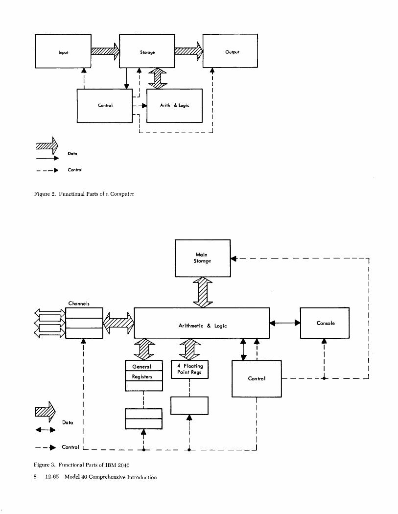
A modern computer (Figure 2) has five distinct functional sections: input, storage, arithmetic and logical circuits, control, and output.
All information to be used by the computer must pass through the input section. The input section interprets information and converts it into a form that the computer can handle. The input section may be one simple device or a big system of input consisting of card readers, magnetic tape units, disk storages, transmission lines, etc.
From the input, the information is directed to the storage section. The main purpose of the storage section is to hold the information necessary to instruct the system in what it has to do, and to serve as an information buffer between input and output sections.
The storage section of a computer consists mostly of a core storage unit with a capacity from a few thouands to many hundreds of thousands of characters, and an access time which is of the same order as the internal processing speed.
The control section directs the operation of the entire system. It receives directions from the storage portion where all instructions for a particular job are stored, prior to processing, in the sequence the machine is expected to execute them.
These instructions obviously must describe the single steps in a code that the control section can recognize and execute. The range of instructions that a computer can execute is relatively small; the instructions themselves are simple. For example, to calculate the square

SIMPLE SYSTEM
2821 Control
CPU
CPU
C H A N N E L
CH 1
CH-2
2803 Tape Control
DUPLEX SYSTEM, SHARED TAPE UNITS
Master
CPU
CPU
Slave
Direct Data Feature
MASTER - SLAVE COMPLEX
C H A N N E L
C H A N N E L
Figure 1. System Configurations
2821 Integrated
Buffer Control
2803 Tape Control
Magnetic Tape Units
2803
Tape Control
Magnetic Tape Units
2821 2821
1403
CH 1
CH 2
2403
Magnetic Tape Units and Control
CPU
2821
2841 Storage Control
1302 - N 1 Disk Storages
2821
1403 1403
Introduction to ~Iodel 40 12-6.5 7
Input
Control
Data
Control
Figure 2. Functional Parts of a Computer
, I ,
Storage
L __
Output
Arith & Logic
I _______ -1
Main Storage - - - - - - - - - - ---1
Channels
Registers
Arithmetic & Logic
, , Control
Data
10 9! I
Control L _ _ _ ___ _ ~ _ _ _ ~ ______ -.J
Figure 3. Functional Parts of IBM 2040
8 12-65 Model 40 Comprehensive Introduction
Console
I I I I
----~---~

root of a number, the operation has to be broken down into a sequence of additions, multiplications, and divisions. A sequence of these steps is called a program.
The arithmetic and logical unit receives data from storage and performs the operations as directed by the control section. Intermediate or final results are put back into storage and then moved to the output section.
The output can be printed, punched into cards, written on magnetic tape or disks, or it can be directly used to control other systems.
Functional Units-System/360 Model 40
• Inputloutput (1/0) units are physically separated from the central computer.
• The central computer is known as the IBM 2040.
• Three channels are provided to control 110 operations.
• In addition to main storage, high-speed data regis-ters can store operands and intermediate results.
• A console contains the necessary operating controls.
Compared with the functional units of a general computer concept, as shown in Figure 2, a more specific breakdown is given in Figure 3.
1. The arithmetic and logic circuitry is the center of all information handling.
2. Main storage is connected as before to this circuitry.
3. I/O information does not flow directly to and from main storage, but passes through the common datahandling section and subsequently through the only main storage access path.
4. Up to three channels are provided to communicate with I/O devices. Channels can be regarded as independent computers to handle I/O operations concurrently with the CPU operations. Once instructed by the CPU they perform all functions necessary to complete an I/O operation on their own, selecting and controlling the I/O device, and perfroming the data transfer to or from main storage.
5. One channel can communicate with several I/O
units. See Figure 1. 6. The time for one main storage cycle 2.5 p.Sec
(read/write) takes four internal process cycles (625 nanoseconds each); therefore, an intermediate storage for efficient data handling is introduced. 16 general, and 4 floating-point registers are provided.
7. For operator and customer engineer controls and interventions, a console panel provides access to all functional parts of the processor.
Introduction to Model 40 12-65 9

Data Formats
• The basic unit of information within the system is the binary bit.
• 8 bits are grouped together to form one byte.
• The byte is the basic unit of information that can be addressed and processed.
• Information can be either in a fixed-length or variable-length format.
• Fixed-length formats are: 1 Byte 2 Bytes = Halfword 4 Bytes = Word 8 Bytes = Double word
• Any operand in main storage is specified by the address of its leftmost byte.
• Fixed-length information must be held in main storage at the proper boundaries.
• Each general register (Figure 3) can store one word.
• Each floating-point register (Figure 3) can store one double word.
• Every byte contains a ninth bit for parity checking.
• Correct parity is always an odd bit count.
Common practice in computers is to refer to each of the individual units of information as a binary bit. Throughout the system all components are always in one of two possible states: a line is active or inactive, a latch is on or off, etc. Components that operate in this manner are said to be binary; the active or on state represents a binary 1, the inactive or off state a binary O.
In order to represent decimal digits, letters, special characters, etc., a combination of several bits has to be used. In System/360, this unit of bit combinations is a group of 8 bits, called one byte. The byte is the basic information block that can be addressed and processed. The byte is also the unit in which the capacity of storage devices is expressed. Bytes may be handled individually or grouped together. A halfword is a group of 2 consecutive bytes. A word is a group of 4 consecutive bytes. A double word is a group of 8 consecutive bytes.
Every general register (Figure 3) can store 4 bytes (word). Every floating-point register can store 8 bytes. ( double word) .
10 12-65 Model 40 Comprehensive Introduction
The location of any field or group of bytes in main storage is specified by the address of its leftmost byte, except during read backward operations when the address specified is that of the rightmost byte.
The length of a field is either implied by the operation to be performed or stated explicitly as part of the instruction. When the length is implied, the information is said to have a fixed length which can be either 1,2,4 or 8 bytes.
Fixed-length information held in main storage must be located at the correct address boundaries. The address (leftmost byte) for any fixed-length information must specify one of the addresses that will be obtained if the complete storage, starting with address 0, would be consecutively filled with that information.
Consequently: Bytes can be stored at any address. Halfwords (2 bytes) must be stored at addresses that are multiples of 2. Words (4 bytes) must be stored at addresses that are multiples of 4. Double words (8 bytes) must be stored at addresses that are multiples of 8.
Within any fixed-length format, the bits making up the format are consecutively numbered from left to right, starting with the number 0 (Figure 4).
When the length of a field is stated explicitly, the information is said to have variable length. Variablelength fields can be from 1 to 256 bytes in increments of one byte; no boundaries have to be observed.
Every byte of information contains a ninth bit, the parity or check bit. Over-all parity per byte is always odd and is always checked when the byte is processed.
Data Coding Information is represented in binary coding. Certain bit configurations can represent other types of coding.
Binary Coding
• The binary system is a place-value number system with the base 2.
• All numbers are expressed with the two symbols o and 1.
• Negative numbers are expressed in two's complementform.
• Binary numbers of various lengths are used within the system.

1 1 Byte 1 o I 0 I I 0 11 I I 0 11 8 B;ts = 1 Byte
o 234567
I I I I I I I I 1 I I I I I I I 1 16 BHs = 2 Bytes = 1 Halfwo.d
o 1 2 3 4 5 6 7 8 15
I I I I I I I I 1 I I I I I I I 1 I ~ ~ I 1 I I I I I I I 132 BHs = 4 Bytes = I Wo.d
o 7 8 15 16 23 24 31
1 I I I I I I I 1 I I I I I I I 1 I W I I 1 I I I I I I I I ~I B~u~l~ ~:~~ o 7 8 1 5 16 55 56 63
Figure 4. Data Formats
• Instructions translate numbers from the decimal to the binary system and vice versa.
The binary number system is a place-value system, as is the decimal system, differing from it in that its base is the number 2 (Figure 5). There are only two symbols, 0 and 1, with which all numbers are expressed. In the decimal system ten symbols are used: 1, 2, 3, 4,5,6, 7, 8, 9, and O.
Examples:
1. The decimal number 209 actually means: (2 X 10²
) + (0 X 101) + (9 X 10°) equally, in the binary system, the number 101 means: (1 X 22) + (0 X 21) + (1 X 2°) 5(decimal) - -
2. The decimal number 6.35 actually means: (6 X 10°) + (3 X 10⁻¹) + (5 X 10⁻²
)
(6 X 10°) X (3 X 1~1) + (5 X 1~2) The binary number 11.01 means: (1 X 21) + (1 X 2°) + (0 X 2-1) + (1 X 2-2
)
( 2 )+( 1 )+( 0 )+(IX ~I!) 3.25 (decimal)
Negative numbers are expressed in complement form. The complement of any number is obtained by subtracting the number from the highest number in the system and adding a one to this intermediate result.
The complement calculated by this method is known as: the two's complement in the binary system and the ten's complement in the decimal system.
Examples: 1. Decimal system - a number system of four positions is
assumed. ten's complement of highest number subtract 15
add 1
15 9999
15
9984 9985
The highest digit position is used to indicate the sign: 0 for positive, 9 for negative. Not all possible numbers are valid in this system; the sign position can only be 0 or 9
Possible numbers in this system range from: Most negative number 9000 ( - 1000 ) Least negative number 9999 ( - 1 ) Zero 0000 (0) Most positive number 0999 (999)
2. Binary system - four-position number system. two's complement of 101 (decimal 5) highest number 1111 subtract 101 101
1010 add 1 1011
The highest digit position is used to indicate the sign: 0 for positive, 1 for negative. All possible numbers in this system are valid.
Numbers in this system range from: Most negative number Least negative number Zero Most positive number
1000 (decimal - 8 ) 1111 (decimal -1) 0000 0111 (decimal 7)
The rule for complementing binary numbers is: invert every bit of the number and add 1.
Example: 0111 - invert: 1000 - add 1: 1001 +7 -7
Recomplementing a negative number follows the same rules discussed previously.
Decimal: 9985 ( -15) 9999
Binary: Invert:
-998.5
0014 + 1
~
1011 (-5) 0100
+ 1 0101
Binary numbers are used for all internal purposes; addressing is always binary (main storage, register,
Data Formats 12-6.5 11

2" 1% 2- Il
1 0 1.0 2 1 0.5 4 2 0.25 8 3 0.125
16 4 0.062 5 32 5 0.031 25 64 6 0.015 625
128 7 0.007 812 5
256 8 0.003 906 25 512 9 0.001 953 125
1 024 10 0.000 976 562 5 2 048 11 0.000 488 281 25
4 096 12 0.000 244 140 625 8 192 13 0.000 122 070 312 5
16 384 14 0.000 061 035 156 25 32 768 15 0.000 030 517 578 125
65 536 16 0.000 015 258 789 062 5 131 072 17 0.000 007 629 394 531 25 262 144 18 0.000 003 814 697 265 625 524 288 19 0.000 001 907 348 632 812 5
1 048 576 20 0.000 000 953 674 316 406 25 2 097 152 21 0.000 000 476 837 158 203 125 4 194 304 22 0.000 000 238 418 579 101 562 5 8 388 608 23 0.000 000 119 209 289 550 781 25
16 777 216 24 0.000 000 059 604 644 775 390 625 33 554 432 25 0.000 000 029 802 322 387 695 312 5 67 108 864 26 0.000 000 014 901 161 193 847 656 25
134 217 728 27 0.000 000 007 450 580 596 923 828 125
268 435 456 28 0.000 000 003 725 290 298 461 914 062 5 536 870 912 29 0.000 000 001 862 645 149 230 957 031 25
1 073 741 824 30 0.000 000 000 931 322 574 615 478 515 625 2 147 483 648 31 0,000 000 000 465 661 287 307 739 257 812 5
4 294 967 296 32 0.000 000 000 232 830 643 653 869 628 906 25 8 589 934 592 33 0.000 000 000 116 415 321 826 934 814 453 125
17 179 869 184 34 0.000 000 000 058 207 660 913 467 407 226 562 5 34 359 738 368 35 0.000 000 000 029 103 830 456 733 703 613 281 25
Figure 5. Powers of Two
12 12-65 Model 40 Comprehensive Introduction

I/O devices). With the basic instruction set only binary arithmetic is provided. Binary numbers within the system can have varying sizes:
Registers are addressed with 4-bit numbers - decimalO to 15. Operation codes are eight-bit numbers - decimal o to 255. MS addresses are 24-bit numbers - decimal 0 to 16,777,215. Halfword arithmetic uses 16-bit numbers - decimal -32,768 to +32,767. General registers store fullword numbers - decimal - 2,147,483,648 to + 2,147,483,647.
Although binary numbers, in general, have more positions than their decimal counterparts (about 3.3 times as many), they are the most suitable numbers to be represented by binary devices (switches, latches, etc. ).
Machine instructions are provided to translate decimal numbers into binary and vice versa. Assembly programs translate decimal values of the programmer to binary for internal use.
Hexadecimal Coding
• Hexadecimal is a place-value system with the base 16.
• Hexadecimal numbers are expressed with 16 different symbols.
• The hexadecimal number system is used in floatingpoint arithmetic.
• One hexadecimal digit represents four binary bits.
• Hexadecimal is a convenient shorthand for writing binary numbers.
Hexadecimal, usually abbreviated to "hex," is a placevalue number system with the base 16. To express any number, 16 diHerent symbols are necessary.
The symbols used by IBM are: Decimal: 0 1 2 3 4 5 6 7 8 9 10 11 12 13 14 15 Hex: 0 1 2 3 4 5 6 7 8 9 ABC D E F
Example: The hex number 1C7 actually means: (1 X 162
) + (C X 161) + (7 X 16°)
(1 X 256) + (12 X 16) + (7 X 1) 455 (decimal)
The hexadecimal number system is used in floatingpoint arithmetic. Every hex digit represents a four-bit binary number.
HEX BINARY
0 0000 1 0001 2 0010 3 0011 4 0100
HEX
5 6 7 8 9 A B C D E F
BINARY
0101 0110 0111 1000 1001 1010 1011 1100 1101 1110 1111
This property of hex digits provides a very useful and simple shorthand for writing large binary numbers.
Examples: 1. A halfword contains the value: Binary 0110 1110 H~ 6 E
0101 5
2. The operation code D2 is actually stored as: 1101 0010
Decimal Coding
1010 A
• Two decimal numbers are packed into one byte ( packed decimal format).
• Every decimal digit is represented by 4 bits.
• Only the combinations for the values 0 to 9 are valid.
• Packed decimal fields are variable in length.
• In a packed decimal field, the lowest-order 4 bits contain a sign code.
Decimal numbers are coded with four-bit binary numbers, two decimal digits per byte. This format is referred to as packed decimal (Figure 6).
Byte Byte Byte Byte
Digit I Digit I Digit I Digit I )) I Digit I Digit Sign
100001011001 o 0 0 0 01000011 1 1 0 1
Figure 6. Packed Decimal Format
Only the binary numbers 0000 to 1001 (0-9 decimal) are valid digit codes.
Codes 1010 to 1111 are used to represent the sign. Interpretation is as follows:
1010 = +ASCIII American Standard Code 1011 = - ASCII f for Information Interchange 1100 = + EBCDICI Extended Binary Coded 1101 = -EBCDICI Decimal Interchange Code 1110 = + I 1111 = + f ( any code)
The sign code generated in decimal arithmetic depends on the character set (ASCII or EBCDIC) and is under program control (Figure 7).
Decimal numbers are treated as signed integers with a variable field-length format from 1 to 16 bytes long. Negative numbers are carried in true form. The sign is stored in the 4 least-significant bits.
Data Formats 12-65 13
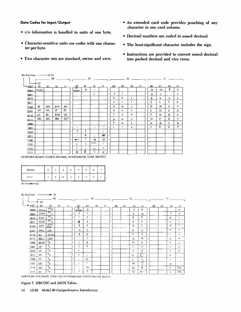
Data Codes for Input/Output
• 110 information is handled in units of one byte.
• Character-sensitive units use codes with one character per byte.
• Two character sets are standard, EBCDIC and ASCII.
Bit Positions ----01
• An extended card code provides punching of any character in one card column.
• Decimal numbers are coded in zoned decimal.
• The least-significant character includes the sign.
• Instructions are provided to convert zoned decimal into packed decimal and vice versa.
~23 L I r--- 00 ~ ___ 01 ,-___ 10 11
'4'i1>7 no 01 10 II 00 01 10 II 00 01 10 11 00 01 10 11
()()(In NULL bl~nk & - "> <: t 0
0001 / '0 i A J 1
0010 b k s B K 5 2
0011 c I t C L T 3
0100 PF RE5 BYP PN d m u D M U 4
0101 HT NL LF R5 e n v E N V 5
0110 LC 'B5 EOB UC f 0 w F 0 W 6
0111 DEL IDL PRE EOT 9 P x G P X 7
1000 h q y H Q Y 8
1001 I " i r z I R Z 9
1010 ? I :
1011 $ I # 1100 - * % @
1101 ( ) ~
1110 + i - = 1111 * ¢ ± ../
EXTENDED BINARY-CODED-DECIMAL INTERCHANGE CODE (EBCDIC)
EBCDIC 0 1 2 3 4 5 6 7
ASCII 7 6 X 5 4 3 2 1
BIT NUMBERING
Bit Positions --------i~~76 L L-X5
_00
4321 00 01 10 11
01 ___ -----,
00 01 10
11 ___ ---,
II 01 10
10 -----,1 '-1 ---
11 00 11 00 01 10
0000 NULL DCO h~nk 0 i5) P p
0001 50M DC
1
0010 EOA DC
2
I 1 i-------'-
2
A Q
B R
0 q
b r
0011 EOM DC3 # 3 C 5 c s
0100 EOT S~::"4 $ 4 D T d t
0101 WRU ERR % 5 E U e u
0110 RU 5YNJ;: & 6 F V f v
0111 BELL LEM 7 G W 9 w
1000 BK5P 50 ( 8 H X h x
1001 HT 51 ) 9 I Y i y
1010 LF ~2 * : J Z i z
1011 VT ~3 + i K C k
1100 FF 54 < L '\. I
1101 CR 55 - = M ] m
1110 50 56 :::::.- N f n ESC
1111 51 57 / ? 0 -- 0 DEL
AMERICAN STANDARD CODE FOR INFORMATION INTERCHANGE (ASCII)
Figure 7. EBCDIC and ASCII Tables
14 12-65 Model 40 Comprehensive Introduction

• Any coding can be used on character-sensitive 1/0
units, since a translate instruction is provided which converts from any code into any other.
All information transfers to and from 110 devices are in units of one byte. Character-sensitive 110 units ( printers, typewriters, card readers and punches) utilize a code in which one character (card column) is represented by one byte. The total number of characters possible is 256. Two standard sets for character coding are used: EBCDIC - Extended Binary Coded
Bit Positions -----.11 __ 01
00 01
00 01 10 11 00 01 10
0000 T09 TE9 E09 TE09 T E 18 18 18 18
0001 T9 E9 09 9 T09 TE9 0 1 1 1 1 1 1 1
0010 T9 E9 09 9 T09 TE9 E09 2 2 2 2 2 2 2
0011 T9 E9 09 9 T09 TE9 E09 3 3 3 3 3 3 3
0100 T9 E9 09 9 T09 TE9 E09 4 4 4 4 4 4 4
0101 T9 E9 09 9 T09 TE9 E09 5 5 5 5 5 5 5
0110 T9 E9 09 9 T09 TE9 E09 6 6 6 6 6 6 6
0111 T9 E9 09 9 T09 TE9 E09 7 7 7 7 7 7 7
1000 T9 E9 09 9 T09 TE9 E09 8 8 8 8 8 8 8
1001 T9 E9 09 9 T E 0 18 18 18 18 18 18 18
1010 T9 E9 09 9 T E TE 28 28 28 28 28 28
I-
1011 T9 E9 09 9 T E 0 38 38 38 38 38 38 38
1100 T9 E9 09 9 T E 0 48 48 48 48 48 48 48
1101 T9 E9 09 9 T E 0 58 58 58 58 58 58 58
1110 T9 E9 09 9 T E 0 68 68 68 68 68 68 68
1111 T9 E9 09 9 T E 0 78 78 78 78 78 78 78
T = 12 Punch E =0 11 Punch
Figure 8. Extended Card Code
Decimal Interchange Code and ASCII - American Standard Code for Information Interchange (Figure 7). Bit numbering is different for the two codes. Corresponding bits are:
EBCDIC: 0 1 2 3 4 5 6 7 (the standard bit numbering within one byte)
ASCII: 7 6 X 5 4 3 2 1 Bits 0-3 are referred to as zone bits, (ASCII: 7-5) Bits 4-7 are referred to as digit bits, (ASCII: 4-1)
An extended card code provides punching of any byte value into one column (Figure 8).
10 11
11 00 01 10 11 00 01 10 11
TEO TO TE EO TEO TO EO 0 0 18 18 18 18 28
TE09 TO TE EO TEO T E E09 1 1 1 1 1 1 1
TE09 TO TE EO TEO T E 0 2 2 2 2 2 2 2 2 2
TE09 TO TE EO TEO T E 0 3 3 3 3 3 3 3 3 3
TE09 TO TE EO TEO T E 0 4 4 4 4 4 4 4 4 4
TEO 9 TO TE EO TEO T E 0 5 5 5 5 5 5 5 5 5
TE09 TO TE EO TEO T E 0 6 6 6 6 6 6 6 6 6
TEO~ TO TE £0 TEO T E 0 7 7 7 7 7 7 7 7 7
TEO~ TO TE EO TEO T E 0 8 8 8 8 8 8 8 8 8
TO TE EO TEO T E 0 18 9 9 9 9 9 9 9 9
TO TE EO TEO T09 TE9 E09 TE09 28 28 28 28 28 28 28 28 28
TO TE EO TEO T09 TE9 E09 TE09 38 38 38 38 38 38 38 38 38
TO TE EO TEO T09 TE9 E09 TE09 48 48 48 48 48 48 48 48 48
TO TE EO TEO T09 TE9 E09 TE09 58 58 58 58 58 58 58 58 58
TO TE EO TEO T09 TE9 E09 TE09 68 68 68 68 68 68 68 68 68
TO TE EO TEO T09 TE9 E09 TE09 78 78 78 78 78 78 78 78 78
o = Zero Punch
Data Formats 12-65 15
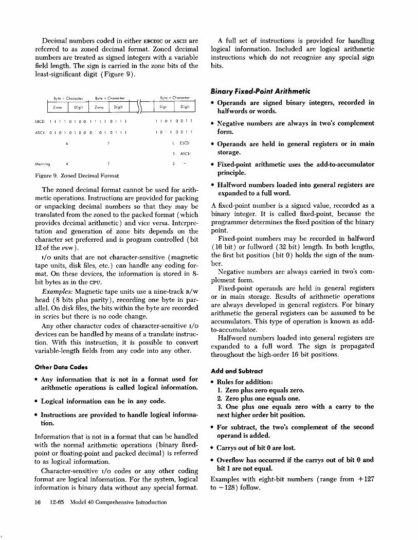
Decimal numbers coded in either EBCDIC or ASCII are referred to as zoned decimal format. Zoned decimal numbers are treated as signed integers with a variable field length. The sign is carried in the zone bits of the least-significant digit (Figure 9).
Byte - Character Byte = Character
EBCD 1 1 1 1 0 1 0 0 1 1 1 1 0 1 1 1 1 1 0 1 0 0 1 1
ASC II 0 1 0 1 0 1 0 0 0 1 0 1 0 1 1 1 1 0 1 1 0 0 1 1
4 L EBCD
S ASCII
Meaning
Figure 9. Zoned Decimal Format
The zoned decimal format cannot be used for arithmetic operations. Instructions are provided for packing or unpacking decimal numbers so that they may be translated from the zoned to the packed format (which provides decimal arithmetic) and vice versa. Interpretation and generation of zone bits depends on the character set preferred and is program controlled (bit 12 of the psw).
I/O units that are not character-sensitive (magnetic tape units, disk files, etc.) can handle any coding format. On these devices, the information is stored in 8-bit bytes as in the CPU.
Examples: Magnetic tape units use a nine-track R/W
head (8 bits plus parity), recording one byte in parallel. On disk files, the bits within the byte are recorded in series but there is no code change.
Any other character codes of character-sensitive I/O
devices can be handled by means of a translate instruction. With this instruction, it is possible to convert variable-length fields from any code into any other.
Other Data Codes
• Any information that is not in a format used for arithmetic operations is called logical information.
• Logical information can be in any code.
• Instructions are provided to handle logical information.
Information that is not in a format that can be handled with the normal arithmetic operations (binary fixedpoint or floating-point and packed decimal) is referred' to as logical information.
Character-sensitive I/O codes or any other coding format are logical information. For the system, logical information is binary data without any special format.
16 12-65 Model 40 Comprehensive Introduction
A full set of instructions is provided for handling logical information. Included are logical arithmetic instructions which do not recognize any special sign bits.
Binary Fixed-Point Arithmetic
• Operands are signed binary integers, recorded in halfwords or words.
• Negative numbers are always in two's complement form.
• Operands are held in general re~isters or in main storage.
• Fixed-point arithmetic uses the add-to-accumulator principle.
• Halfword numbers loaded into general registers are expanded to a full word.
A fixed-point number is a signed value, recorded as a binary integer. It is called fixed-point, because the programmer determines the fixed position of the binary point.
Fixed-point numbers may be recorded in halfword (16 bit) or fullword (32 bit) length. In both lengths, the first bit position (bit 0) holds the sign of the number.
Negative numbers are always carried in two's complement form.
Fixed-point operands are held in general registers or in main storage. Results of arithmetic operations are always developed in general registers. For binary arithmetic the general registers can be assumed to be accumulators. This type of operation is known as addto-accumulator.
Halfword numbers loaded into general registers are expanded to a full word. The sign is propagated throughout the high-order 16 bit positions.
Add and Subtract
• Rules for addition: 1. Zero plus zero equals zero. 2. Zero plus one equals one. 3. One plus one equals zero with a carry to the next higher order bit position.
• For subtract, the two's complement of the second operand is added.
• Carrys out of bit 0 are lost.
• Overflow has occurred if the carrys out of bit 0 and bit 1 are not equal.
Examples with eight-bit numbers (range from + 127 to -128) follow.
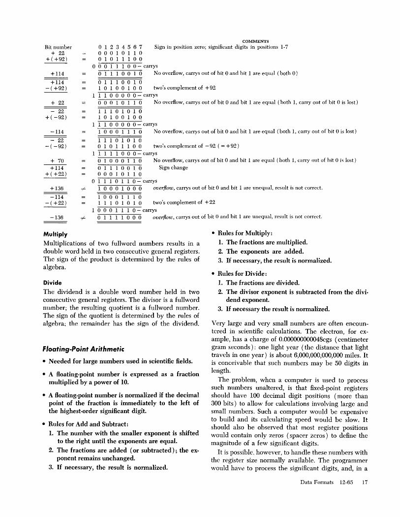
COMMENTS
Bit number + 22
+( +92)
o 1 2 3 4 5 6 7 000 1 0 1 1 0 010 1 1 100
Sign in position zero; significant digits in positions 1-7
o 0 0 1 1 1 0 0 - carrys
+114
+114 -( +92)
o 1 1 1 0 0 1 0 No overflow, carrys out of bit 0 and bit 1 are equal (both 0)
o 1 1 100 1 0 1 0 1 0 0 1 0 0 two's complement of +92
1 1 1 0 0 0 0 0 - carrys
+ 22
- 22 + ( -92)
o 0 0 1 0 1 1 0 No overflow, carrys out of bit 0 and bit 1 are equal (both 1, carry out of bit 0 is lost)
1 110 1 0 1 0 1 0 100 1 0 Q
1 1 1 0 0 0 0 0 - carrys -114 1 0 0 0 1 1 1 0 No overflow, carrys out of bit 0 and bit 1 are equal (both 1, carry out of bit 0 is lost)
- 22 -( -92)
1 1 1 0 1 0 1 0 010 1 1 100 two's complement of - 92 ( = + 92 )
1 1 1 1 1 0 0 0 - carrys
+ 70 +114
+( +22)
o 1 0 0 0 1 1 0 No overflow, carrys out of bit 0 and bit 1 are equal (both 1, carry out of hit 0 is lost) o 1 1 1 0 0 1 0 Sign change 000 1 0 1 1 0
o 1 1 1 0 1 1 0 - carrys +136
-114
1 0 0 0 1 0 0 0 overflow, carrys out of bit 0 and bit 1 are unequal, result is not correct.
- (+22) 1 000 1 1 1 0 1 1 1 0 1 0 1 0 two's complement of + 22
1 0 0 0 1 1 1 0 - carrys -136 o 1 1 1 1 0 0 0 overflow, carrys out of bit 0 and bit 1 are unequal, result is not correct.
Multiply
Multiplications of two fullword numbers results in a double word held in two consecutive general registers. The sign of the product is determined by the rules of algebra.
Divide
The dividend is a double word number held in two consecutive general registers. The divisor is a fullword number; the resulting quotient is a fullword number. The sign of the quotient is determined by the rules of algebra; the remainder has the sign of the dividend.
Floating-Point Arithmetic
• Needed for large numbers used in scientific fields.
• A floating-point number is expressed as a fraction multiplied by a power of 10.
• A floating-point number is normalized if the decimal point of the fraction is immediately to the left of the highest-order significant digit.
• Rules for Add and Subtract: 1. The number with the smaller exponent is shifted
to the right until the exponents are equal.
2. The fractions are added (or subtracted); the exponent remains unchanged.
3. If necessary, the result is normalized.
• Rules for Multiply: 1. The fractions are multiplied.
2. The exponents are added.
3. If necessary, the result is normalized.
• Rules for Divide: 1. The fractions are divided.
2. The divisor exponent is subtracted from the dividend exponent.
3. If necessary the result is normalized.
Very large and very small numbers are often encountered in scientific calculations. The electron, for example, has a charge of 0.OOOOOOOOOO48cgs (centimeter gram seconds): one light year (the distance that light travels in one year) is about 6,000,000,000,000 miles. It is conceivable that such numbers may be 50 digits in length.
The problem, when a computer is used to process such numbers unaltered, is that fixed-point registers should have 100 decimal digit positions (more than 300 bits) to allow for calculations involving large and small numbers. Such a computer would be expensive to build and its calculating speed would be slow. It should also be observed that most register positions would contain only zeros (spacer zeros) to define the magnitude of a few significant digits.
It is possible, however, to handle these numbers with the register size normally available. The programmer would have to process the significant digits, and, in a
Data Formats 12-65 17
separate sequence, would have to establish the position of the decimal point which often (at the time of programming) is not easily predictable.
Thus, the need for a shorthand notation and a simplified arithmetic (floating-point) becomes apparent for those areas where the magnitude of numbers covers a wide range.
The key to floating-point data representation is the separation of the significant digits of a number from the size (magnitude) of the number. Thus, the number is expressed as a fraction multiplied by a power of 10.
Exponential Numbers
1. In the decimal system, 0.00000000048 actually means: (0 x 10°) + (0 X 10-1
) + ... + (4 X 10⁻¹⁰) + (8 X 10-11
)
All terms except the last two are zero; the number can be written as: ( 4 x 10⁻¹°) + (8 X 10-11
)
In order to simplify this expression, the second term is transformed into a number with the same power-of-ten factor as in the first. (4 x 10⁻¹⁰
) (.8 x lO- JO)
( 4.8) x 10-10
4.8 X 10⁻¹⁰
.48 X 10-9 ( nonnalized )
2. In the decimal system, 6,000,000,000,000 actually means: (6 x 10¹²
) + (0 X 1011) + ... + (0 x 10°) 6 X 10¹²
.6 X 1013
Whenever the decimal point is moved one position to the left, the power-of-ten (exponent) is increased by one.
Whenever the decimal point is moved one position to the right the exponent is decreased by one.
A floating-point number is normalized, if, in the fraction, no spacer zeros are carried. The decimal point is immediately to the left of the highest-order significant digit.
Rules for Add and Subtract
1. The number with the smaller exponent is shifted to the right until the exponents are equal.
2. The fractions are added (or subtracted), the exponent remains unchanged.
3. If necessary the result is normalized. Example: 21,700,000 + 800 = (.217 X 108
) + (.8 X 103)
= .217 X 108
+ .000008 X 108
.217008 X 108
Rules for Multiply
Shift right until exponents are equal.
1. The fractions are multiplied.
18 12-65 Model 40 Comprehensive Introduction
2. The exponents are added.
3. If necessary the result is normalized. Example: 2500 X 0.000000033 = (.25 X 104
) X (.33 X 10-7)
Multiply fractions: .25 X .33 = .0825 Add exponents: (+4) + (-7) = -3 Result: .0825 X 10-3
N onnalized: .825 X 10-4
Rules for Divide
1. The fractions are divided.
2. The divisor exponent is subtracted from the dividend exponent.
3. If necessary the result is normalized. Example:
0.000222 + 0.00004 = (.222 X 10-3) + (.4 x 1O-~)
Divide fractions: .222 + .4 = .555 Subtract exponents: ( -3) - (-4) = + 1 Result: .555 X 10
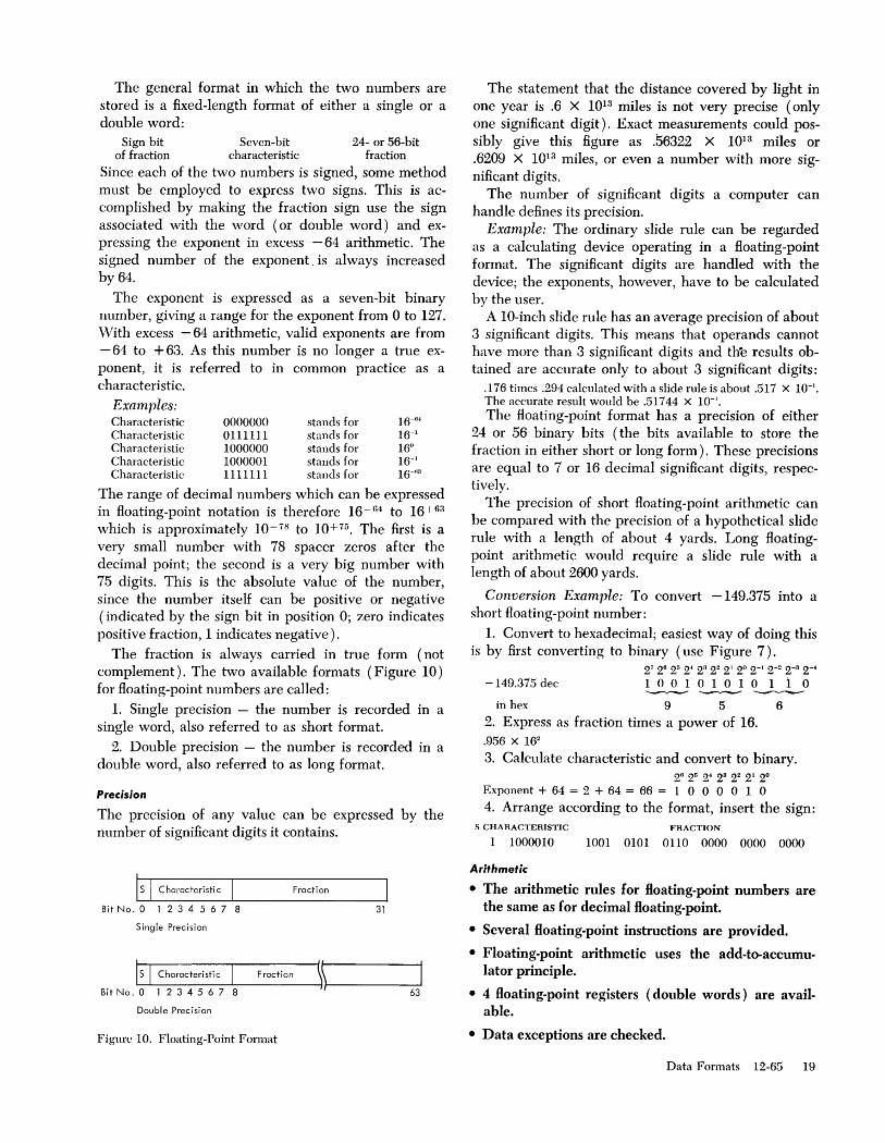
Floating-Point Notation
Format
• Floating-point numbers are recorded in the hexadecimal number system.
• The significant digits are recorded as hexadecimal fractions.
• The exponent (called the characteristic) is a sevenbit binary number to which the base 16 is raised.
• The characteristic can be a number from 0 to 127.
• Floating-point numbers are recorded in a fixedlength format:
short precision in single words double precision in double words
• Bit 0 in either format denotes the sign of the fraction.
• Negative fractions are always carried in true form.
Floating-point numbers are recorded in the hexadecimal number system.
Example: The hexadecimal number 1C.A actually means:
(1 x lW) + (C x 16°) + (A x 16-1)
To express this number in the floating-point format, the exponents have to be equal and the signincant digits are expressed as a fraction:
(.1 X 162) + (.OC X 162
) + (.OOA X 162)
.ICA X 162
In order to store such a number in the machine, two values have to be recorded:
1. The fraction (.lCA).
2. The power to which 16 has to be raised ( + 2 ).
The base is always 16; as this fact is implicit in the operations the number is not recorded.
The general format in which the two numbers are stored is a fixed-length format of either a single or a double word:
Sign bit Seven-bit 24- or 56-bit of fraction characteristic fraction
Since each of the two numbers is signed, some method must be employed to express two signs. This is accomplished by making the fraction sign use the sign associated with the word (or double word) and expressing the exponent in excess - 64 arithmetic. The signed number of the exponent. is always increased by 64.
The exponent is expressed as a seven-bit binary number, giving a range for the exponent from 0 to 127. \Vith excess - 64 arithmetic, valid exponents are from - 64 to + 63. As this number is no longer a true exponent, it is referred to in common practice as a characteristic.
Examples: Characteristic 0000000 stands for 16-64
Characteristic 0111111 stands for 16-1
Characteristic 1000000 stands for 16° Characteristic 1000001 stands for 1W1
Characteristic 1111111 stands for 16+d3
The range of decimal numbers which can be expressed in floating-point notation is therefore 16- 64 to 16+ 63
which is approximately 10-. 78 to 10+ 75 • The first is a very small number with 78 spacer zeros after the decimal point; the second is a very big number with 75 digits. This is the absolute value of the number, since the number itself can be positive or negative (indicated by the sign bit in position 0; zero indicates positive fraction, 1 indicates negative).
The fraction is always carried in true form (not complement). The two available formats (Figure 10) for floating-point numbers are called:
l. Single precision - the number is recorded in a single word, also referred to as short format.
2. Double precision - the number is recorded in a double word, also referred to as long format.
Precision
The precision of any value can be expressed by the number of significant digits it contains.
IS I Characteristic I Fraction
Bit No. 0 1 2 3 4 5 6 7 8 31
Single Precision
IS I Characteristic Fraction )) 63 Bit No. 0 1 2 3 4 5 6 7 8
Double Precision
Figure 10. Floating-Point Format
The statement that the distance covered by light in one year is .6 X 1013 miles is not very precise (only one significant digit). Exact measurements could possibly give this figure as .56322 X 1013 miles or .6209 X 1013 miles, or even a number with more significant digits.
The number of significant digits a computer can handle defines its precision.
Example: The ordinary slide rule can be regarded as a calculating device operating in a floating-point format. The significant digits are handled with the device; the exponents, however, have to be calculated by the user.
A 10-inch slide rule has an average precision of about 3 significant digits. This means that operands cannot have more than 3 significant digits and the results obtained are accurate only to about 3 significant digits:
.176 times .294 calculated with a slide rule is about .517 X 10-1. The accurate result would be .51744 X 10-1. The floating-point format has a precision of either
24 or 56 binary bits (the bits available to store the fraction in either short or long form). These precisions are equal to 7 or 16 decimal significant digits, respectively.
The precision of short floating-point arithmetic can be compared with the precision of a hypothetical slide rule with a length of about 4 yards. Long floatingpoint arithmetic would require a slide rule with a length of about 2600 yards.
Conversion Example: To convert -149.375 into a short floating-point number:
l. Convert to hexadecimal; easiest way of doing this is by first converting to binary (use Figure 7).
-149.375 dec 27 26 25 24 23 22 21 2° 2-1 2-2 2-3 2- i
100101010110
in hex 9 5 6
2. Express as fraction times a power of 16. .956 X 162
3. Calculate characteristic and convert to binary. 26 25 24 23 22 21 2°
Exponent + 64 = 2 + 64 = 66 = 1 0 0 0 0 1 0
4. Arrange according to the format, insert the sign: S CHARACTERISTIC FRACTION
1 1000010 1001 0101 0110 0000 0000 0000
Arithmetic
• The arithmetic rules for floating-point numbers are the same as for decimal floating-point.
• Several floating-point instructions are provided.
• Floating-point arithmetic uses the add-to-accumulator principle.
• 4 floating-point registers (double words) are available.
• Data exceptions are checked.
Data Formats 12-65 19

Arithmetic operations are executed by the computer as explained for decimal floating-point numbers.
To handle floating-point nuinbers, various instructions are provided.
Floating-point arithmetic uses the add-to-accumulator principle; the accumulators in this case are the 4 double word floating-point registers. It is implied in floating-point operations that these registers are used ( and not general registers).
The instructions available include the following types:
Add Subtract Multiply Divide
Compare Load floating-point register Store floating-point register
All instructions are provided for the short and long format. The results are automatically normalized except for the special operations: add unnormalized and subtract unnormalized.
During execution of the operation, several unusual conditions can be detected and indicated to the program:
Exponent Overflow: The result characteristic in addition, subtraction, multiplication, or division exceeds 127, and the result fraction is not zero. The operation is completed, and a program interrupt occurs. The fraction is normalized, and the sign and fraction of the result remain correct. The result characteristic is made 128 smaller than the correct characteristic. For addition and subtraction, the condition code is set to 1 when the result is less than zero, and the condition code is set to 2 when the result is greater than zero. For multiplication and division, the condition code remains unchanged.
Exponent Underflow: The result characteristic in addition, subtraction, multiplication, halving, or division is less than zero and the result fraction is not zero. The operation is completed, and a program interrupt occurs if the exponent-underflow mask bit (psw bit 38) is l.
The setting of the mask bit also affects the result of the operation. When the mask bit is 0, the sign, characteristic, and fraction are set to zero, thus making the result a true zero. When the mask bit is 1, the fraction is normalized, the characteristic is made 128 larger than the correct characteristic, and the sign and fraction remain unchanged.
Significance Exception: The resulting fraction of add or subtract operations is zero.
Divide Exception: Division by a number with a zero fraction is attempted. The operation is suppressed. There are no instructions to translate floating-point numbers to and from other number systems. Conver-
20 1-68 Model 40 Comprehensive Introduction
sion has to be programmed; conversion routines are included in the assembly programs.
Decimal Arithmetic
• Packed decimal is used in decimal arithmetic.
• The storage-to-storage principle is used.
• Negative numbers are carried in true form with the corresponding sign.
• Multiply and divide are performed as a sequence of add or subtract operations.
• Decimal arithmetic is performed in a binary adder; the numbers have to be modified accordingly.
The number format used in decimal arithmetic is the packed decimal format. Instructions available include:
Zero and Add Add Subtract MultipJy Divide Compare
Decimal arithmetic uses the storage-to-storage principle. Both operands are held in main storage and have a variable field length. The result is stored back into main storage and replaces the first operand.
Negative numbers are always carried in true form with the corresponding sign in the lowest-order 4 bits.
Prior to instruction execution, the operand signs are analyzed to determine whether a true or complement add operatIOn has to take place.
Multiply and divide are performed as a sequence of add or subtract operations.
Decimal arithmetic is performed in a binary adder; the decimal numbers have to be modified accordingly.
Rules for True Dec:imal Add
1. A correction 6 is always added to each digit of the first operand.
2. Binary add the second operand.
3. If the high-order bit position of a packed decimal digit (bit value 8) generates a carry, the result is correct.
4. If this bit position does not generate a carry, the result has to be decreased by 6 ( add two's complement of 6 which is 1010). Ignore the decimal carry that may occur.

Example:
38 +47
----s5 binary add 6 to first operand digits
add second operand
add 10 10 to decimal digits without carry
ignore digit carrys decimal result
R.ules for Complement Add
Bit 0 1 2 3 '4 5 6 7 o 0 1 1: 1 0 0 0 o 1 0 0,0 1 1 1
, 0011'1000 o 1 1 0:0 1 1 0 1 0 0 1'1 1 1 0 o 1 0 0:0 1 1 1
NC C,
C
1 1 1 0:0 1 0 1 , 1 0 1 0,0 0 0 0 , , 1 0 0 0 10 1 0 1
8 I 5 I
1. No corrections of 6 to first operand.
2. Add two's complement of second operand.
3. If the high-order bit position of the packed decimal digit (bit value 8) generates a carry, the result is correct.
4. If this bit position does not generate a carry, the result has to be decreased by 6 ( add two's complement of 6 which is 1010).
5. If a sign change occurs, the result has to be recomplemented (subtract result from zero).
Example:
47 = -75 = -28
Add two's complement of second operand
Add 1010 to digits without carry
Carry out indicates sign change!
Recomplement: (complement add to 0 and change sign)
Add 10 10 to digits without carry
Ignore digit carries decimal result
Bit 0 1 2 3' 4 5 6 7 o 1 0 0 10 1 1 1 o 1 1 1:0 101
I o 1 0 0,0 1 1 1 , 1 0 0 Ot! 0 1 1
NC C'
C
1 1 0 1'0 0 1 0 1 0 1 0:0 0 0 0
o 1 1 1'0 0 1 0 I
o 0 0 010 0 0 0 1 0 0 011 1 1 0
NC NC: 1 0 0 0,1 1 1 0 1 0 1 0,1 0 1 0
C C I
o 0 1 0; 1 0 0 0 -2 8
Data Formats 1-68 21

System Controls
Instructions • Instructions can be one, two, or three halfwords.
• Instructions must be located on integral halfword boundaries.
The length of a machine instruction can be one, two, or three halfwords. It is related to the ntimber of storage addresses necessary for performing the operation.
An instruction consisting of only one halfword cannot cause any reference to main storage. An instruction that is two halfwords long provides one storage address and a three-halfword instruction provides two storage addresses. All instructions must be located in storage on integral halfword boundaries. An integral halfword boundary is any 24-bit address whose low-order bit is O.
First Halfword 1
Format Type Byte 1 I Byte 2 I 1 I
I I , Register Register , Operand 1 Operand 2 1 ~~
RR Register -to-register I Op Code I Rl I R2 I 10 718 1112 151
1 I Register I I
1 Operand 1 1 , ~,
RX Register-to-indexed-I Op Code I
Rl I X2 I B2 storage
10 718 1112 .15:16 1 I
Register Register 1 Operand 1 Operand 3 1 ,---A--..,~(
RS Reg i ste r-to-storage
I Op Code
I Rl
I R3
I B2
10 7,8 11 12 15116
1 I Immediate I 1 I Operand I 1 , '\I
SI Storage and immed-
I OpCode
I I iate operand 12 Bl
10 7,8 15,16 I I Length I
I Operand 1 Operand 2 1 ~~,
SS Storage-to-storage I OpCode I L 1 I
L2 I
Bl
Instruction Format
• The first byte of an instruction contains the operation code (op code).
• Up to 256 op codes possible.
• The five instruction formats are RR, RX, RS, Sl and SSe
The first halfword of an instruction (Figure 11) consists of two parts. In the first part, bits 0-7 are the op code. Provision is made for up to 256 op codes by using the eight-bit binary format.
The second part of the first halfword, bits 8-15, may be used as a register specification, a mask, an operand length specification, a byte of immediate data, or it may be ignored. Immediate data are held in the instruction format and used as one of the operands.
Second Halfword 2 Third Halfword 3
, 1 1 , , 1 , ,
Address Operand 2
, \
I D2 J 1920
Address I Ope:and 2 I
\
I D2
I I 1920 311 I
Address 1 I Operand 1 I I
1
I J 1 Dl I
1920 I Address 1 Address I Ope~and 1 1 Oper~nd 2 I
" \
I Dl
I B2
I D2 I
o 78 1112 1516 1920 31 47
Figure 11. Five Basic Instruction Formats
22 12-65 Model 40 Comprehensive Introduction

The second and third halfwords, when present in the instruction, always have the same format. This format is a four-bit base address register (B), followed by a twelve-bit displacement address (D).
For purposes of describing the execution of instructions, operands are designated as first, second, and third operands. These names refer to the manner in which the operands participate. The operand to which a field in an instruction format applies is generally denoted by the number following the code name of the field, for example, Rl, Bl, L2, D2•
The length and format of an instruction are specified by the first two bits of the op code.
BTT POSITIONS
(0-1 ) 00 01 10 11
INSTRUCTION LENGTH CODE
INSTRUCTION
LENGTH
One halfword Two halfwords Two halfwords
Three halfwords
INSTRUCTION
FORMAT
RR RX
RS or SI SS
Bits 8-15 of the instruction are used either as two four-bit fields or as a single eight-bit field. This byte can contain the following information:
Four-bit operand register specification (Rl, R~, or R:) Four-bit index register specification (X2 )
Four-bit mask (Ml) Four-bit operand length specification (L1 or L2) Eight-bit operand length specification (L) Eight-bit byte of immediate data (12 )
In some instructions, a four-bit field (the whole second byte of the first halfword) is ignored.
The second and third halfwords always have the same format: four-bit base register designation (Bl or B2 ) followed by a twelve-bit displacement (Dl or D2)'
Address Generation
• Base address is a 24-bit number contained in the general register specified by the instruction B-field.
• Index address is a 24-bit number contained in the general register specified by the instruction X-field.
• Displacement address is a 12-bit number contained in tlte instruction D-field.
• An actual main storage address is formed by adding the contents of B to the contents of X plus D.
• Main storage addresses referring to fixed-length information must observe the boundary specifications.
For addressing purposes, operands can be grouped in three classes: (1) explicitly addressed operands in main storage, (2) immediate operands placed as part of the instruction stream in main storage, and (3) operands located in the general or floating-point register.
To permit the ready relocation of program segments and to provide for flexible specifications of input, out-
put, and working areas, all instructions referring to main storage have been given the capacity of employing a full address of 24 bits, regardless of the actual storage size of the individual system.
The address used to refer to main storage is generated from three binary numbers: the base address ( B ), the index (X), and the displacement (D).
Base Address (B)
The base address (B) is a 24-bit number contained in a general register specified by the program in the B-field of the instruction. The B-field is included in every MS address specification. The base address can be used as a means of static relocation of programs and data.
In array-type calculations, the base address can specify the location of an array and, in record-type processing, it can identify the record. The base address provides for addressing the entire main storage. The base address may also be used for indexing purposes.
Index (X)
The index (X) is a 24-bit number contained in a general register specified by the program in the X-field of the instruction. It is included only in the address specified by the RX instruction format. The index can be used to provide the address of an element within an array. Thus, the RX format instructions permit double indexing.
Displacement (D)
The displacement (D) is a 12-bit number contained in the instruction format. It is included in every instruction that addresses main storage. The displacement provides for relative addressing up to 4095 bytes beyond the element or base address.
In array-type calculations, the displacement may be used to specify one of the many items associated with an element. In the processing of records, the displacement can be used to identify items within a record.
In forming the actual MS address, the base address and index are treated as unsigned 24-bit positive binary integers. The displacement is similarly treated as a 12-bit positive binary integer. The three are added as 24-bit binary numbers, ignoring overflow. Since every address includes a base, the sum is always 24 bits long. The general register bits used for addressing are bits 8-31. Bits 0-7 are ignored.
The program may have zeros in the base address, index, or displacement fields. A zero is used to indicate the absence of the corresponding address components. A base or index of zero implies that a zero quantity is to be used in forming the address regardless of the contents of general register O. A displacement of zero has no special significance.
System Controls 12-65 23
Initialization, modification, and testing of base addresses and indices can be carried out by fixed-point instructions: branch and link, branch on count, or branch on index.
M:S addresses referring to fixed-length data formats must specify the proper address boundaries. If the boundary specifications are not met, a program check occurs.
Instruction Types
• Only a basic set of instructions is provided as standard equipment; additional instruction sets are optional.
• Instruction types provided are: Data handling instructions Branch instructions 110 instructions System control instructions.
• Data handling instructions are available for: Fixed-point data Floating-point data Decimal data Logical information.
The instructions available are listed in Figure 12. For detailed explanation of instructions, refer to IBM System/360 Principles of Operation, Order No. GA22-6821.
Only a basic set of these instructions is provided with the standard machine; additional instruction sets are optional. The terminology used for various instruction sets is as follows:
1. Standard instruction set.
2. Commercial instruction set - standard instruction set plus decimal feature instructions.
3. Scientific instruction set - standard instruction set plus floating-point feature instructions.
4. Universal instruction set - includes all instructions (Figure 12) except the two direct control instructions (marked Y). Four types of instructions can be distinguished:
a. Data-handling instructions - perform arithmetic or logical operations with the data specified by the operands (actual data-processing functions within the system).
h. Branch instructions - allow change in sequence of program instructions.
c. Input/output instructions-control I/O devices and data transfers between CPU and I/O equipment.
d. System control instructions - control the over-all system status.
24 12-65 Model 40 Comprehensive Introduction
Data-Handling Instructions
• Arithmetic and logical instructions are provided.
• Depending on the data format processed, the in-structions are called:
Fixed-point instructions Floating-point instructions Decimal instructions Logical instructions
The arithmetic instructions are provided for all data formats and with various specifications of their operands (operands in general registers or main storage).
Fixed-point instructions handle fixed-point data (signed binary integers); floating-point instructions handle floating-point data. Decimal instnlctions handle packed decimal data. Logical instructions handle any type of data but without special treatment of the positions used for sign representation of some formats.
Instructions performing other than arithmetic operations are called logical instructions. A set of instructions which performs logical operations on the operands and instructions that are used for data-handling (and format) belongs to this group.
Arithmetic
Add: 15 add instructions are provided: Fixed-point instructions:
AR - RR format, fullwords A - RX format, fullwords AH - RX format, halfwords
Floating-point instructions: ADR - RR format, normalized long AD - RX format, normalized long AER - RR format, normalized short AE - RX format, normalized short A WR - RR format, unnormalized long A \V - RX format, unnom1alized long A UR - RR format, unnormalized short AU - RX format, unnormalized short
Decimal instructions: AP - 55 format, variable length ZAP - 55 format, variable length
J ,ogical instructions: ALR - RR format, binary add without special handling of
sign AL - RX format
In all formats, the second operand is added to the first operand; the result replaces the first operand.
A similar range of instructions is provided for other arithmetic operations.
Subtract: The second operand is subtracted from the first operand; the result replaces the first operand.
f..fultiply: The product of the multiplier (second operand) and the multiplicand (first operand) replaces the multiplicand.
In fixed-point arithmetic, the result contains 64 bits. Rl must specify an even-numbered general register;

NAME MNEMONIC TYPE EXCEPTIONS CODE NAME MNEMONIC TYPE EXCEPTIONS CODE
Add AR RR C IF lA Halt 110 HIO SI CM 9E Add A RX C A,S, IF SA Halve (Long) HDR RRF S,V 24 Add Decimal AP SS T,C P,A, D, DF FA Halve (Short) HER RRF S,U 34 Add Halfword AH RX C A,S, IF 4A Insert Character IC RX A 43 Add Logical ALR RR C IE Insert Storage Key ISK RRZ M, A,S 09 Add Logical AL RX C A,S, 5E Load LR RR 18 Add Normalized Load L RX A,S 58 (Long) ADR RRF,C S,U,E,LS 2A Load Address LA RX 41 Add Normalized Load and Test LTR RR C 12 ( Long) AD RXF,C A,S,V,E,LS 6A Load and Test Add Normalized ( Long) LTDR RRF,C S 22 ( Short) AER RRF,C S,V,E,LS 3A Load and Test Add Normalized ( Short) LTER RRF,C S 32
( Short) AE RXF,C A,S,U,E,LS 7A Load Complement LCR RR C IF 13 Add Vnnorm- Load Complement alized (Long) AWR RRF,C S, E,LS 2E ( Long) LCDR RRF,C S 23 Add Unnorm- Load Complement alized (Long) AW RXF,C A,S, E,LS 6E ( Short) LCER RRF,C S 33 Add Unnorm- Load Halfword LH RX A,S 48
alized (Short) AUR RRF,C S, E,LS 3E Load (Long) LDR RRF S 28 Add Unnorm- Load (Long) LD RXF A,S 68 alized (Short) AU RXF,C A,S, E,LS 7E Load Multiple LM RS A,S 98 AND NR RR C 14 Load Negative LNR RR C 11 AND N RX C A,S 54 Load Negative AND NI SI C P,A 94 (Long) LNDR RRF,C S 21 AND NC SS C P,A D4 Load Negative Branch and Link BALR RR 05 ( Short) LNER RRF,C S 31 Branch and Link BAL RX 45 Load Positive LPR RR C IF 10 Branch on Load Positive
Condition BCR RR 07 (Long) LPDR RRF,C S 20 Branch on Load Positive
Condition BC RX 47 ( Short) LPER RRF,C S 30 Branch on Count BCTR RR 06 LoadPSW LPSW SI LM, A,S 82 Branch on Count BCT RX 46 Load (Short) LER RRF S 38 Branch on Index Load (Short) LE RXF A,S 78
High BXH RS 86 Move MVI SI P,A 92 Branch on Index Move MVC SS P,A D2
Low or Equal BXLE RS 87 Move Numerics MVN SS P,A DI Compare CR RR C 19 Move with Offset MVO SS P.A FI Compare C RX C A,S 59 Move Zones MVZ SS P,A D3 Compare Decimal CP SS T,C A, D F9 Multiply MR RR S lC Compare Halfword CH RX C ~,S 49 Multiply M RX A,S 5C Compare Logical CLR RR C 15 Multiply Decimal MP SS T P,A,S,D FC Compare Logical CL RX C A,S 55 Multiply Halfword MH RX A,S 4C Compare Logical CLI SI C A 95 Multiply (Long) MDR RRF S,U,E 2C Compare Logical CLC SS C A D5 Multiply (Long) MD RXF A,S,U,E 6C Compare (Long) CDR RRF,C S 29 Multiply (Short) MER RRF S,U,E 3C Compare (Long) CD RXF,C A,S 69 Multiply (Short) ME RXF A,S,.u,E 7C Compare (Short) CER RRF,C S 39 OR OR RR C 16 Compare (Short) CE RXF,C A,S 79 OR 0 RX C A,S 56 Convert to Binary CVB RX A,S,D, IK 4F OR 01 SI C P,A 96 Convert to Decimal CVD RX P,A,S 4E OR OC SS C P,A D6 Diagnose SI M, A,S 83 Pack PACK SS P,A F2 Divide DR RR S, IK ID
Read Direct RDD SI Y M,P,A 85 Divide D RX A,S, IK 5D Divide Decimal DP SS T P,A,S,D, DK FD Set Program Mask SPM RR L 04 Divide (Long) DDR RRF S,U,E,FK 2D Set Storage Key SSK RRZ M, A,S 08 Divide (Long) DD RXF A,S,U,E,FK 6D Set System Mask SSM SI M, A 80 Divide (Short) DER RRF S,U,E,FK 3D Shift Left Double SLDA RS C S, IF 8F Divide (Short) DE RXF A,S,U,E,FK 7D Shift Left Double
Logical SLDL RS S 80 Edit ED SS T,C P,A, D, DE Shift Left Single SLA RS C IF 8B Edit and Mark EDMK SS T,C P,A, D, DF Shift Left Single Exclusive OR XR RR C 17 Logical SLL RS 89 Exclusive OR X RX C A,S 57 Shift Right Double SRDA RS C S 8E Exclusive OR XI SI C P,A 97 Shift Right Double Exclusive OR XC SS C P,A D7 Logical SRDL RS S 8C Execute EX RX A,S, EX 44
Figure 12. Alphabetic List of Instructions (Sheet 1 of 2)
System Controls 1-68 25

NAME MNEMONIC TYPE EXCEPTIONS CODE
Shift Right Single SRA RS C 8A Shift Right Single
Logical SRL RS 88 Start 110 SIO SI CM 9C Store ST RX P,A,S 50 Store Character STC RX P,A 42 Store Halfword STH RX P,A,S 40 Store (Long) STD RXF P,A,S 60 Store Multiple STM RS P,A,S 90 Store (Short) STE RXF P,A,S 70 Subtract SR RR C IF IB Subtract S RX C A,S, IF 5B Subtract Decimal SP SS T,C P,A, D, DF FB Subtract Halfword SH RX C A,S, IF 4B Subtract Logical SLR RR C IF Subtract Logical SL RX C A,S 5F Subtract Norm-
alized (Long) SDR RRF,C S,U,E,LS 2B Subtract Norm-
alized (Long) SD RXF,C A,S,U,E,LS 6B Subtract Norm-
alized (Short) SER RRF,C S,U,E,LS 3B
LEGEND
MNEMONIC:
Mnemonic Used For Programming
TYPE:
Instruction Type (RR, RX, RS, SI, SS) and Instruction Set which provides the Instruction (No Indication = Standard Set) F: Floating Point Feature T: Decimal Feature Y: Direct Control Feature Z: Protection Feature
C: Indicates that the Instruction sets the Condition Code
CODE:
Operation Code in Hexadecimal
Figure 12. Alphabetic List of Instructions (Sheet 2 of 2 )
the result is stored in the even/odd register pair specified by Rl.
In decimal arithmetic, the multiplier size is limited to 15 digits and must be less than the number of multiplicand digits to give a maximum of 31 digits in the result.
Divide: The dividend (first operand) is divided by the divisor (second operand), and the quotient and the remainder replace the dividend.
In fixed-point arithmetic, the dividend Rl must specify an even/odd register pair; the relative size of
26 12-65 Model 40 Comprehensive Introduction
NAME MNEMONIC TYPE EXCEPTIONS CODE
Subtract Norm-alized (Short) SE RXF,C A,S,U,E,LS 7B
Subtract Unnorm-alized (Long) SWR RRF,C S, E,LS 2F
Subtract Unnorm-alized (Long) SW RXF,C A,S, E,LS 6F
Subtract Unnorm-ali zed (Short) SUR RRF,C S, E,LS 3F
Subtract Unnorm-ali zed (Short) SU RXF,C A,S, E,LS 7F
Supervisor Call SVC RR OA
Test Channel TCH SI CM 9F Test 110 TIO SI CM 9D Test Under Mask TM SI C A 91 Translate TR SS P,A DC Translate and Test TRT SS C A DD
Unpack UNPK SS P,A F3
Write Direct WRD SI Y M, A 84
Zero and Add ZAP SS T,C P,A, D, DF F8
EXCEPTION:
Program Checks detected during Instruction Execution: A: Main Storage Address Specification D: Data Format or Coding
DF: Decimal Overflow DK: Decimal Divide Exception
E: Exponent Overflow EX: Execute Exception FK: Floating Point Divide Exception IF: Fixed Point Overflow IK: Fixed Point Divide Exception LS: Significance Exception M: Privileged Operation P: Protection Exception S: SpeCification Exception U: Exponent Underflow
dividend and divisor must be such that the quotient does not exceed 31 bits.
In decimal arithmetic, the maximum size of the dividend is 31 digits. The relative size of dividend and divisor must be such that the quotient does not exceed 15 digits.
Compare: The first and second operands are compared; the result is related to the first operand (low - the first operand is less than the second operand). The first operand is not destroyed.
Shift Left or Right: All shift operations are in the RS format. The content of Rl is shifted the number of
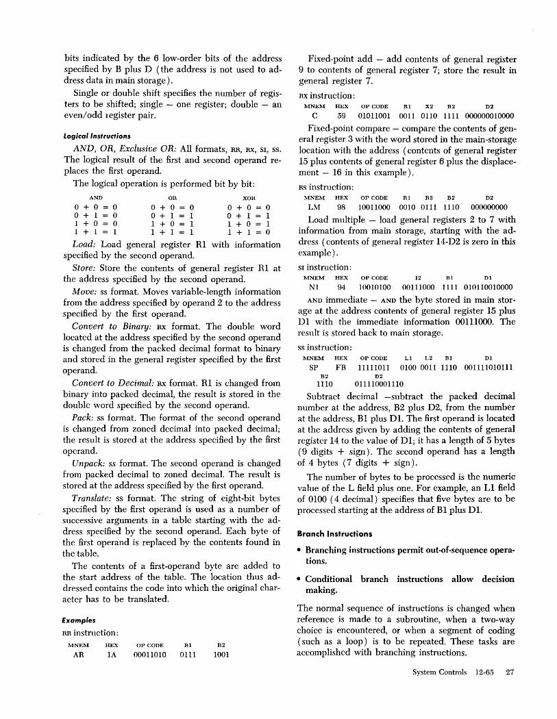
bits indicated by the 6 low-order bits of the address specified by B plus D (the address is not used to address data in main storage).
Single or double shift specifies the number of registers to be shifted; single - one register; double - an even/ odd register pair.
Logicallnstrudions
AND, OR, Exclusive OR: All formats, RR, RX, SI, SS.
The logical result of the first and second operand replaces the first operand.
The logical operation is performed bit by bit:
AND
o + 0 = 0 o + 1 0 1 + 0 = 0 1 + 1 = 1
o + o + 1 + 1 +
OR
0=0 1 1 o = 1 1 = 1
XOR
o + 0=0 o + 1 = 1 1 + o = 1 1 + 1 = 0
Load: Load general register Rl with information specified by the second operand.
Store: Store the contents of general register Rl at the address specified by the second operand.
Move: ss format. Moves variable-length information from the address specified by operand 2 to the address specified by the first operand.
Convert to Binary: RX format. The double word located at the address spedfied by the second operand is changed from the packed decimal format to binary and stored in the general register specified by the first operand.
Convert to Decimal: RX format. Rl is changed from binary into packed decimal, the result is stored in the double word specified by the second operand.
Pack: ss format. The format of the second operand is changed from zoned decimal into packed decimal; the result is stored at the address specified by the first operand.
Unpack: ss format. The second operand is changed from packed decimal to zoned decimal. The result is stored at the address specified by the first operand.
Translate: ss format. The string of eight-bit bytes specified by the ,first operand is used as a number of successive arguments in a table starting with the address specified by the second operand. Each byte of the first operand is replaced by the contents found in the table.
The contents of a first-operand byte are added to the start address of the table. The location thus addressed contains the code into which the original character has to be translated.
Examples
RR instruction: MNEM HEX
AR lA OP CODE RI
00011010 0111 R2
1001
Fixed-point add - add contents of general register 9 to contents of general register 7; store the result in general register 7.
RX instruction: MNEM HEX OP CODE RI X2 B2 D2
C 59 01011001 0011 0110 1111 000000010000
Fixed-point compare - compare the contents of general register 3 with the word stored in the main-storage location with the address (contents of general register 15 plus contents of general register 6 plus the displacement - 16 in this example).
RS instruction: MNEM HEX OP CODE RI R3 B2 D2
LM 98 10011000 0010 0111 1110 000000000
Load multiple - load general registers 2 to 7 with information from main storage, starting with the address (contents of general register 14-D2 is zero in this example).
Sl instruction: MNEM HEX OP CODE 12 BI DI
N 1 94 10010100 00111000 1111 010110010000
AND immediate - AND the byte stored in main storage at the address contents of general register 15 plus Dl with the immediate information 00111000. The result is stored back to main storage.
ss instruction: MNEM HEX OP CODE LI L2 BI DI
SP FB 11111011 0100 0011 1110 001111010111 B2 D2
1110 011110001110
Subtract decimal -subtract the packed decimal number at the address, B2 plus D2, from the number at the address, Bl plus Dl. The first operand is located at the address given by adding the contents of general register 14 to the value of Dl; it has a length of 5 bytes (9 digits + sign). The second operand has a length of 4 bytes (7 digits + sign).
The number of bytes to be processed is the numeric value of the L field plus one. For example, an Ll field of 0100 (4 decimal) specifies that five bytes are to be processed starting at the address of Bl plus Dl.
Branch Instructions
• Branching instructions permit out-of-sequence operations.
• Conditional branch instructions allow decision making.
The normal sequence of instructions is changed when reference is made to a subroutine, when a two-way choice is encountered, or when a segment of coding (such as a loop) is to be repeated. These tasks are accomplished with branching instructions.
System Controls 12-65 27

Subroutine linkage permits not only the introduction of a new instruction address but also the preservation of the return address and associated information.
Decision-making is provided by the branch on condition instruction. This instruction inspects a two-bit condition code that reHects the result of a majority of the arithmetic, logical, and 110 operations.
Each of these operations can set the code in any of four states; the conditional branch can specify any selection of these four states as the criterion for branching. For example, the condition code reHects such conditions as result non-zero, first operand high, overHow, channel busy, etc. Once set, the condition code remains unchanged until modified by an instruction that reHects a different condition code. The two bits of the condition code provide for ,four possible condition code settings: 0, 1, 2, and 3. The specific meaning of any setting is significant only to the operation setting the condition code.
Loop control can be performed by the conditional branch when it tests the outcome of address arithmetic and counting operations. For some particularly frequent combinations of arithmetic and tests, the instructions branch on count and branch on index are provided. These branches, being specialized, provide increased performance for these tasks.
Branch on Condition
RR - Op Code (BCR, 07) MI, R2 RX - Op Code (BC, 47) MI, X2, B2, D2
The condition code is investigated as specified by the four-bit mask, M1. If the condition is satisfied, the current instruction counter (Ie) value is replaced by the address specified by operand 2 (RR: contents of general register R2; RX: address specified by B2 + X2 + D2). If the condition is not satisfied, Ie remains unchanged and the next sequential instruction is executed.
The condition code can be any of the following combinations, depending on the result of the last instruction e~ecuted that affects the code.
The four-bit mask in bit positions 8-11 of the instruction corresponds, left to right, with the four condition code settings:
00 01 10 11 Bit 8 9 10 11
The branch is successful whenever the present condition code matches a corresponding mask bit of 1. Multiple mask bits are permissible.
Examples:
1. A branch should occur if the condition code is 00: the mask must specify: 1000.
2. A branch should occur if the condition code is not 00: the mask must specify: 0111.
28 12-65 Model 40 Comprehensive Introduction
3. For an unconditional branch, the mask is 1111. 4. For no operation, the mask is 0000. 5. Any other combination is possible.
Branch and link
RR - op code (BALR, 05) Rl, R2. RX - op code (BAL, 45) Rl, X2, B2, D2.
Branch and link is an unconditional branch. The current Ie, together with other psw information (bits 32-63), is stored in the general register specified by R1. Subsequently, the address specified by operand 2 (RR: contents of general register R2, RX: address specified by B2 + X2 + D2) replaces the current Ie.
This instruction is normally used for subroutine linkage. The return address from the subroutine to the main program is preserved in the register specified.
Branch On Count
RR - op code (BCTR, 06) Rl, R2. RX - op code (BCT, 46) Rl, X2, B2, D2.
The contents of the general register specified by Rl are treated as a 32-bit fixed-point integer and algebraically reduced by 1 every time this instruction is executed.
As long as the result in Rl is not zero, the current Ie is replaced by the address specified in the second operand; consequently, a branch takes place. If the result is zero, Ie remains unchanged and the next sequential instruction is executed.
The subtraction is performed prior to testing for zero result.
This instruction is used if part of the main program has to be looped a predetermined number of times.
Execute
RX - op code (EX, 44) Rl, X2, B2, D2. Branch instruction to execute one single instruction outside the normal instruction sequence.
The single instruction at the address specified by operand 2 (B2 + X2 + D2) is modified by the contents of general register Rl and executed. Note that this instruction must not be another execute.
Bits 8-15 of the instruction designated by the branch address are OR' ed with bits 24-31 of Rl. The contents of Rl or the instruction held in storage are not changed by this operation.
The Ie is updated by 4, unless the instruction executed is a successful branch instruction. In this case, the current Ie is replaced by the new Ie introduced.
Sequential Instruction Execution • Instructions are executed sequentially under con
trol of an instruction counter (Ie).
• The instruction counter is updated as instructions are executed.
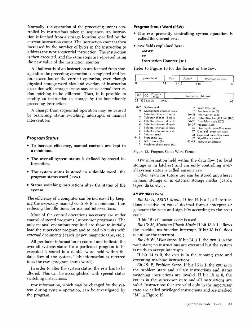
Normally, the operation of the processing unit is controlled by instructions taken in sequence. An instruction is fetched from a storage location specified by the current instruction count. The instruction count is then increased by the number of bytes in the instruction to address the next sequential instruction. The instruction is then executed, and the same s'teps are repeated using the new value of the instruction counter.
All halfwords of an instruction are fetched from storage after the preceding operation is completed and before execution of the current operation, even though physical storage-word size and overlap of instruction execution with storage access may cause actual instruction fetching to be different. Thus·, it is possible to modify an instruction in storage by the immediately preceding instruction.
A change from sequential operation may be caused by branching, status switching, interrupts, or manual intervention.
Program Status
• To increase efficiency, manual controls are kept to a minimum.
• The over-all system status is defined by stored information.
• The system status is stored in a double word: the program status word (psw).
• Status switching instructions alter the status of the system.
The efficiency of a computer can be increased by keeping the necessary manual controls to a minimum, thus reducing the idle times for manual interventions'.
Most of the control operations necessary are under control of stored programs (supervisor programs). The only manual operations required are those to initially load the supervisor program and to load I/O units with external documents (cards, paper, magnetic tape, etc. ).
All pertinent information to control and indicate the over-all systems status for a particular program to be executed is stored in a double word held within the data flow of the system. This information is referred to as the psw (program status word).
In order to alter the system status, the psw has to be altered. This can be accomplished with special status switching instructions.
psw information, which may be changed by the system during system operation, can be investigated by the program.
Program Status Word (PSW)
• The psw presently controlling system operation is called the current psw.
• psw fields explained here: AMWP
cc Instruction Counter (IC).
Refer to Figure 13 for the format of the psw.
I System Mask Key I AMWP Interruption Code
o 78 1112 1516 31
0-7 System mask o Multiplexor channel mask 1 Selector channell mask 2 Selector channe I 2 mask 3 Selector channel 3 mask 4 Selector channel 4 mask 5 Selector channel 5 mask 6 Selector channel 6 mask 7 External mask
8-11 Protection key 12 ASCII mode (A) 13 Machine check mask (M)
Instruction Address
14 Wait state (W) 15 Problem state (P)
16-31 I nterruption code
63
32-33 Instruction Length Code (ILC) 34-35 Condition code (CC) 36-39 Program mask
36 Fixed-point overflow mask 37 Decimal overflow mask 38 Exponent underflow mask 39 Sign i fi cance mask
40-63 Instruction address
Figure 13. Program Status Word Fonnat
psw information held within the data flow (in local storage or in latches) and currently controlling overall system status is called current psw.
Other psw's for future use can be stored anywhere: in main storage or in external storage media (cards, tapes, disks, etc. ) .
AMWP (Sits 12-15)
Bit 12: A, ASCII Mode: If bit 12 is a 1, all instructions sensitive to zoned decimal format interpret or generate the zone and sign bits according to the ASCII
code. If bit 12 is 0, EBCDIC code is used. Bit 13: M, Machine Check Mask: If bit 13 is 1, allows
the machine malfunction interrupt. If bit 13 is 0, does not allow the interrupt.
Bit 14: W, Wait State: If bit 14 is 1, the CPU is in the wait state; no instructions are executed but the system is ready to accept interrupts.
If bit 14 is 0, the CPU is in the running state and executing machine instructions.
Bit 15: P, Problem State: If bit 15 is 1, the CPU is in the problem state and all I/O instructions and status switching instructions are invalid. If bit 15 is 0, the CPU is in the supervisor state and all instructions are valid. Instructions that are valid only in the supervisor state are called privileged instructions and are marked "M" in Figure 12.
System Controls 12-65 29
Problem programs are normally run in problem state to ensure that instructions that may affect the over-all system status are invalid. These privileged instructions may not be executed unnoticed by the supervisor program, which is the only program in charge of systems control. Supervisor programs are always run with bit 15 of the psw = o.
Condition Code (Sits 34 and 35)
• The condition code is set by certain machine instructions according to the result obtained.
• The condition code has different meanings for different instructions.
• The condition code can be investigated by branch on condition.
The condition code in the psw is set according to the result of certain machine instructions. The instructions that set the condition code are those marked C in Figure 12. Other instructions leave the condition code unchanged.
The result reHected in the condition code depends on the instruction executed. General forms are shown below.
The condition code can be investigated by the branch on condition instructions.
INSTRUCTION CONDITION CODE
00 01 10 11
Arithmetic operations: result is: 0 <0 >0 Overflow
Compare operations: result is: equal low high -
Logical operations (AND, OR, XOR) result is: 0 #0 - -
I/O operations, the addressed unit is: available exceptional busy not ready
condition present
Instruction Counter (Bits 40-63)
• 24-bit MS address of the next sequential instruction.
• IC is updated during instruction fetch by the number of bytes in the current instruction.
• During successful branch instructions, the IC is re-placed by the branch address specified.
The instruction counter (Ie) always contains the MS
address of the next sequential instruction. The Ie originally loaded into the psw specifies the MS address of the first instruction to be executed.
During sequential instruction execution, the Ie is updated during the instruction-fetch phase by the number
30 12-65 Model 40 Comprehensive Introduction
of bytes the new instruction contains; i.e. by 2 for RR
instructions; by 4 for RX, RS, and SI instructions; or by 6 for ss instructions.
After a successful branch instruction, the current Ie
is replaced by the branch address specified, and instruction fetch is resumed from this new location.
Status Switching Instructions
• Instructions that alter part of the current psw or introduce a new psw are called status switching instructions.
• Generally, status switching instructions are valid only if the system is in supervisor state (bit 15 of the current psw = 0).
Load PSW
SI format: op code (LPSW, 82), bits 8-15 ignored, BI, DI.
The double word located at the MS address specified by Bl plus D1 replaces the entire current psw.
Set Program Masle
RR format: op code (SPM, 04), R1 bits 12-14 ignored.
Bits 2-7 of the general register specified by R1 replace bits 34-39 of the current psw (condition code and program mask).
Exception: This instruction is valid in problem state.
Set System Masle
SI format: op code (SSM, 80), bits 8-15 ignored, B1, Dl.
The byte located at the MS address specified by BI plus Dl replaces the system mask (bits 0-7) of the current psw.
Interrupt System
• The interrupt system increases the efficiency of the programmed system control.
• All conditions that occur asynchronously to the normal sequential instruction execution are signalled to the system by a program interrupt.
• Three interrupt types: (1) always accepted by the system, (2) can be masked off but remains pending, and (3) can be masked off and ignored.
• Acceptance of an interrupt automatically stores current psw: interrupt handling is determined by the program.
The efficiency of over-all system control by the psw is further increased by the interrupt concept.
Conditions arise that are asynchronous with sequential instructions. These conditions can be anticipated

by the program (e.g. completion of a previously initiated I/O operation, inquiries from transmission terminals, etc.) or the conditions may occur with no relation to the over-all program flow (unexpected conditions, e.g. program checks, machine malfunctions). All these conditions are signalled to the system at the time of occurrence by a program interrupt.
For anticipated conditions, no special programming is necessary (periodic interrogation of status latches during the main program). Unexpected conditions do not necessarily stop the system, and consequently do not always require manual operator interventions to resume system operation. Program checks never stop the system; machine malfunctions do so only if a permanent system failure exists.
Anticipated interrupts are accepted by the system only if the system is in wait state or after completion of the instruction during which the interrupt is signalled.
Unexpected interrupts (program or machine checks) are taken as soon as they occur.
Certain program check interrupts are always accepted by the system.
The majority of all possible interrupts can be masked off by programming (set up of psw). When masked off, they are not accepted by the system at the time they occur, but remain pending until the psw is changed (by programming) .
Certain program check interrupts can be masked off and ignored (exceptional conditions masked off by the program mask, bits 36-39 of psw).
The only system operation performed when a program interrupt is accepted is replacement of the current psw.
The current psw is stored at a predetermined main storage location and is subsequently referred to as old psw. Depending on the type of interrupt, an interruption code is set into this old psw.
From another predetermined MS location a new psw is fetched, which now becomes the current psw controlling further systems operation. In particular, the IC of the new psw indicates a program segment in main storage that performs the necessary decisions and contains the instructions to handle the present interrupt.
Since all pertinent information of the interrupted program is preserved in the old psw, this program can be resumed after interrupt handling at the exact point of interruption and with the same over-all system status as at the time of interruption.
Types of Interrupts
• Five types of interrupts: 11o, external, supervisor call, program check, and machine check.
• Each type of interrupt has two related psw's, old and new, held in main storage.
I/O Interrupts
An I/O interrupt provides a means by which the CPU
responds to conditions in the channels and I/O units. An I/O interrupt can occur only for the channel
whose system mask bit (bit 0, 1, or 2) is a one. The address of the channel and I/O unit involved are recorded in the old psw. Further information concerning the I/O operation is preserved in the channel status word (csw) that is stored during the interruption.
External Interrupts
The external interrupt provides the means by which the CPU responds to signals from the interruption key on the system control panel, the timer, and the external signals of the direct control feature.
An external interrupt can occur only when the system mask bit 7 is a one.
Supervisor-Call Interrupt
This interrupt occurs as a result of execution of supervisor call instruction.
A major use for the svc instruction is to switch from a problem program to the supervisor program.
It is the only instruction available in problem state (psw bit 15 = 1) that provides a means of status switching. During execution of this instruction ( RR
format: op code (svc, OA), HI, H2) the current psw is replaced by the new svc psw and the 8 bits HI, R2 are set into the interruption code of the old svc pw.
Program-Check Interrupt
Unusual conditions encountered in a program create a program check interrupt. These conditions include incorrect operands and operand specifications, as well as exceptional results.
Machine-Check Interrupt
The occurrence of an intermittent machine malfunction (if not disabled by psw bit 13 = 0) terminates the current instruction, initiates a diagnostic procedure, and subsequently causes the machine-check interrupt. A machine check cannot be caused by invalid data or instructions.
Each type of interrupt has two related psw's, old and new, stored at predetermined main storage locations.
If any program interrupt occurs, the type of interrupt is indicated to the system by the MS location from which the new psw is fetched, i.e. the pre-stored new psw's indicate different interrupt handling routines (IC).
Permanent Main Storage Locations
• The old and new psw's for the various interruption types are stored at fixed locations.
• Other essential control information have locations.
System Controls 12-65 31

• Permanent MS locations should not he used for other data.
Permanent MS locations are shown in Figure 14. Locations other than those used for old and new
psw's are explained in the appropriate sections of this introduction.
The locations specified may not he used as storage for other data without devaluating the system concept. However the interrupt system provided can be completely ignored and most functions could be programmed. The locations for old and new psw's would then be available for other purposes; but, the system efficiency would drop considerably.
Priority of Interrupts
• Only one interrupt of anyone type can he present at a time.
• Simultaneously occurring interrupts of diHerent types are accepted in a predetermined priority.
• The sequence in which interrupts are handled is the reverse sequence of their acceptance.
The I/O interrupts may be requested by several units operating concurrently; however, only one interrupt can be accepted by the system at anyone time. External interrupts may be requested by several sources. They are oR'ed together and accepted as one interrupt. For other interrupt types, only one interrupt at a time is possible.
During the execution of an instruction, several interrupt requests of different types may occur simultaneously. Simultaneous interrupts are accepted in the following predetermined order:
ADDRESS LENGTH PURPOSE
0 00000000 double-word Initial program loading PSW 8 0000 1000 double-word Initial program loading CCW 1
16 0001 0000 double-word Initial program loading CCW2 24 00011000 double-word External old PSW 32 0010 0000 double-word Supervisor call old PSW 40 0010 1000 double-word Program old PSW 48 0011 0000 double-word Machine-check old PSW 56 0011 1000 double-word Input/output old PSW 64 01000000 double-word Channel status word 72 0100 1000 word Channel address word 76 01001100 word Unused 80 01010000 word Timer 84 0101 0100 word Unused 88 0101 1000 double-word External new PSW 96 01100000 double-word Supervisor call new PSW
104 0110 1000 double-word Program new PSW 112 0111 0000 double-word Machine-check new PSW 120 0111 1000 double-word Input/output new PSW 128 10000000 Diagnostic scan-out area 0
o The size of the diagnostic scan-out area depends on the par-ticular model and I/O channels.
Figure 14. Permanent Storage Assignments
32 12-65 Model 40 Comprehensive Introduction
Machine check Program check or supervisor call External Input/ output
The program-check and supervisor-call interrupts are mutually exclusive and cannot occur at the same time.
When more than one interrupt source requests service, the action consists of storing the old psw and fetching the new psw belonging to the interruption that is taken first. This new psw is subsequently stored without any instruction execution, and the next interrupt psw is fetched. This process continues until no more interrupts are to be serviced.
vVhen the last interrupt request has been serviced, instruction execution is resumed using the psw last fetched. The order of execution of the interrupt subroutines is, therefore, the reverse of the order in which psw's are fetched.
Thus, the most important interrupts, I/O and external, are actually serviced first.
Machine check, when it occurs, does not allow any other interrupts to be recognized.
Masking of Interrupts in PSW
• Most interrupts can he prevented hy zero mask hits in the current psw.
• Masked interrupts remain pending until the appro-priate mask hit are set to one.
I/O Interrupts
The I/O interrupts are masked in the system mask of the psw.
The individual channels can be masked independently in bits 0-6. In the IBM 2040, only the first three bits are significant:
Bit 0 for the multiplex channel. Bit 1 for selector channell. Bit 2 for selector channel 2. \Vhen a mask bit is 1, the source can interrupt the
cpu; with a mask bit of 0, the source cannot interrupt but the interrupt remains pending.
External Interrupts
External interrupts are masked in bit 7 of the system mask.
Although different sources for external interrupts exist, there is only one mask bit (bit 7) that allows all sources to interrupt.
1: interrupts are allowed and accepted 0: interrupts are not allowed but remain pending.
Supervisor-Call Interrupts
Supervisor-call interrupts cannot be masked off and are taken whenever a supervisor-call instruction is executed.

Program Check Interrupts
Some exceptional conditions which may arise during arithmetic operations can be masked by the program mask of the psw. When the appropriate bits are 1, the interrupts are accepted; when the bits are 0 the interrupts are ignored.
Bit 36: Fixed Point Overflow: masks program-check interrupts generated by overflows in fixed-point arithmetic.
Bit 37: Decimal Overflow: masks program-check interrupts generated by overflows in decimal arithmetic.
Bit 38: Exponent Underflow: masks program-check interrupts generated if the exponent in floating-point arithmetic is less than - 64.
Bit 39: Significance: masks program-check interrupts generated if the resulting fraction in floating-point add or subtract operation is zero.
Other program-check interrupts cannot be masked and are always accepted.
M'achine-Check Interrupts
Machine check interrupts are masked in bit 13 of the psw (machine check mask). If bit 13 = 1, intermittent machine malfunctions genmate a machine check interrupt. If bit 13 = 0, machine check interrupts are not accepted but remain pending.
Interrupt Code in PSW
• The interrupt code, stored in bits 16-31 of the old psw during the interrupt sequence, identifies the source of the interrupt.
I/O Interrupts
Old psw stored in main storage location 38 hex, interruption source is identified as follows:
0000 0000 aaaa aaaa U nit on MPX channel 0000 0001 aaaa aaaa Unit on SC 1 0000 0010 aaaa aaaa Unit on SC 2 a .... a = device address of the unit that caused the interrupt.
External Interrupts
Old psw stored in main storage location 18 hex, interrupt source is identified as follows:
Bits 16-23 are always zero, Bits 24-31 as follows: x x x x x x x 1 External signal 7 x x x x x x 1 x External signal 6 x x x x x 1 x x External signal 5 x x x x 1 x x x External signal 4 x x x 1 x x x x External signal 3 x x 1 x x x x x External signal 2 x 1 x x x x x x Console interrupt key 1 x x x x x x x Timer x = Unpredictable external interrupts from different sources
are oR'ed and accepted as one interrupt. Consequently, more than a single 1 bit may be present in the interrupt code.
Supervisor-Call Interrupt
Old psw stored in MS location 20 hex, interruption source is identified as follows:
Bits 16-23 are always zero, Bits 24-31 contain bits 8-15, of the svc instruction.
Program-Check Interrupt
Old psw stored in MS location 28 hex, interruption source is identified as follows:
Bits 16-27 are always zero, Bits 28-31 as follows (instructions affected as in
Figure 12).
0001 Invalid Operation: occurs when an operation code is unassigned or the operation code is not available on the particular machine.
0010 Privileged Operation: occurs when the CPU is operating in the problem program state and a privileged instruction is given. Privileged instructions are indicated by M.
0011 Execute: occurs when the instruction designated by an execute instruction is another execute instruction. Instruction affected: EX.
0100 Protection: occurs when the storage key of an addressed location does not match the protection key in the PSW. Instruction affected: P.
0101 Addressing: occurs when an address specifies any part of data, an instruction, or a control word outside the available main storage area for the particular installation. Instruction affected: A.
0110 Specifications: occurs when: 1. A data word, instruction word, or control word
address does not specify an integral boundary for the unit of information.
2. The Rl field of an instruction specifies an odd register address for a pair of general registers that contain a 64-bit operand.
3. A floating-point register address other than 0, 2, 4, or 6 is specified.
4. In decimal arithmetic, the multiplier or divisor exceeds 15 digits and sign.
5. The first operand field is shorter than, or equal to, the second operand field in decimal multiplication or division.
6. The block address specified in set storage key instruction or insert storage key instruction does not contain all zeros in the four low-order bit positions. Instruction affected: S.
0111 Data: occurs when: 1. The sign or digit codes of operands are incorrect
in decimal arithmetic, convert to binary, or editing. 2. Fields in decimal arithmetic overlap incorrectly. 3. The decimal multiplicand has too many high
order significant digits. Instruction affected: D.
System Controls 12-65 33

1000 Fixed-Point Overflow: occurs when a highorder carry is generated or high-order significant bits are lost in fixed-point add, subtract, or shift operations. The interrupt is under control of the program mask. Instruction affected: IF.
1001 Fixed-Point Divide: occurs when a quotient exceeds the register size in fixed-point divide. For division by zero, the instruction is suppressed. If the result of the convert to binary instruction exceeds 31 bits, the instruction is completed and lost information is ignored. Instruction affected: IK.
1010 Decimal Overflow: occurs when the destination field is too small to contain the result field. The interrupt is under control of the program mask. Instruction affected: DF.
1011 Decimal Divide: occurs when a quotient exceeds the specified data field size. Instruction affected: DK.
1100 Exponent Overflow: occurs when the result characteristic in addition, subtraction, multiplication, or division exceeds 127, and the result fraction is not zero. The operation is completed, and a program interrupt occurs. The fraction is normalized, and the sign and fraction of the result remain correct. The result characteristic is made 128 smaller than the correct characteristic. For addition and subtraction, the condition code is set to 1 when the result is less than zero, and the condition code is set to 2 when the result is greater than zero. For multiplication and division, the condition code remains unchanged.
1101 Exponent Underflow: occurs when the result characteristic in addition, subtraction, multiplication, halving, or division is less than zero and the result fraction is not zero. The operation is completed, and a program interrupt occurs if the exponent-underflow mask bit (psw bit 38) is l.
The setting of the mask bit also affects the result of the operation. When the mask bit is 0, the sign, characteristic, and fraction are set to zero, thus making the result a true zero. When the mask bit is 1, the fraction is normalized, the characteristic is made 128 larger than the correct characteristic, and the sign and frac-_ tion remain unchanged.
1110 Significance: occurs when the result is an allzero fraction in floating-point add or subtract. The interrupt is under control of the program mask. Instruction affected: LS.
1111 Floating-Point Divide: occurs when attempting to divide by a floating-point number with an all-zero fraction. Instruction affected: FK.
Machine Check Interrupt
Old psw stored in MS location 30 hex. Bits 16-31 are set to zero's.
34 1-68 Model 40 Comprehensive Introduction
Instruction Length Code (lLC) in PSW
The instruction length code is stored in psw bits 32, 33 and identifies the instruction length of the last instruction executed.
For some interrupts, it is desirable to locate the instruction that was being interpreted when the interrupt occurred. Since the instruction address in the old psw designates the instruction to be executed next, it is necessary to know the length of the preceding instruction. This length is recorded in bit positions 32 and 33 of the psw as the instruction length code.
The instruction length code is meaningful only for program check and supervisor-call interrupts. For I/O
and external interrupts, the interruption is not caused by the last-interpreted instruction, and the code is not meaningful for these instructions. For machine-check interrupts, the setting of the code may be affected by the malfunction and, therefore, is unpredictable.
For the supervisor-call interrupt, the instruction length code is 1, indicating the halfword length of supervisor call. For program check interruptions, the codes 1, 2, and 3 indicate the instruction length in halfwords.
The code 0 is reserved for program check interruptions where the length of the instruction is not available because of certain overlapping conditions in instruction fetching. In code 0 cases, the instruction counter in the old psw does not represent the next instruction address. Instruction length code 0 can occur for a program check interruption only when the interruption is caused by a protected or an unavailable data address.
The following tables shows the states of the instruction length code.
psw BITS INSTRUCTION
ILC 32-33 LENGTH FORMAT
0 00 Not available 1 01 One halfword RR 2 10 Two halfwords RX, RS or SI 3 11 Three halfwords SS
CPU Status
• CPU status is determined by four types of programstate alternatives.
• The CPU state alternatives are named: stopped or operating running or waiting masked or interruptible supervisor or problem state
• The states differ in the way they affect CPU functions and in the manner their status is indicated and switched.
• All CPU states are independent of each other.

Stopped or Operating State
The stopped state is entered and left under manual control. Instructions are not executed, interrupts are not accepted, and the timer is not updated. In the operating state, the CPU is capable of executing instructions and being interrupted.
Running or Waiting State
In the running state, instruction fetching execution proceeds in the normal manner. The wait state is normally entered by the program to await an interruption, for example, an I/O interruption or operator intervention from the console.
In the wait state, no instructions are processed, the timer is updated, and I/O and external interruptions are
System Controls 1-68 34.1

accepted unless masked. Running or waiting state is determined by the setting of bit 14 in the psw.
Masked or Interruptible State
The CPU may be interruptible or masked for interruptions. The interruptible states of the CPU are changed by changing the mask bits of the psw.
Supervisor or Problem State
In the problem state, all I/O instructions and privileged instructions are invalid and cause a program check interrupt. In the supervisor state, all instructions are valid. The choice of problem or supervisor state is determined by bit 15 of the psw.
" Standard Interface
l I I Integrated Console
Control Unit Typewriter
I J~ Card Printer
Read I Punch
) Standard Interface
l I Tape File
Control A Control A
1 I I r 1
Tape Tape Tape Disk Disk Drive Drive Drive Drive Drive
0 1 2 0 1
) Standard Interface
~ I I Tape File
Control B Control B
1 1 I I -- 1
Tape Tape Disk Disk Drive Drive Drive Drive
0 1 0' 1
Figure 15. Sample System Configuration
110 System
Sample System Configuration
In order to explain the basic I/O system architecture, a sample configuration is introduced. See Figure 15. In the follOWing sections, reference is made to this figure to show the over-all relationship of functional units and operations.
IBM 2040 Processing Unit: Functional units within the central processor in relation to I/O operations are:
1. CPU circuits - all internal data How and control circuits of the processor.
Multiplex Channel
Main Storage
Permanent Locations
CPU Program
Selector Channel
CPU -Circuits Data
1
Channel Programs
1 Mpx Store r
Selector Channel
2
System Controls 12-65 35

2. Main storage - storage unit that holds all the information required for internal processing (programs and data), destination for input information, and the source for output information.
Channels: are independent control units for input/ output operations. Three channels are available:
Multiplex channel, standard Selector channell, optional Selector channel 2, optional
Control Units: Units that provide the necessary functions for the control of particular I/O devices and translate between device language and channel language.
1. Integrated Control Unit - controls card reader, card punch and printer for concurrent operations; translates between internal data coding and card code, and provides data buffers for a complete card or print line.
2. Tape Control Unit - controls tape drive functions for up to eight drives and provides a single data path between channel and tape drives.
3. File Control - controls disk storage functions for up to eight disk drives provides a single data path between channel and one disk drive; translates between the serial bit representation on disks and the parallel coding of the channel.
I/O Devices: are units that control information external to the system (cards, printing, magnetic tape, disks) .
1. IBM 1052 Console Typewriter - communication between operator and system.
2. IBM 2540 Card Reader/Punoh - functionally, two independent units for card reading and punching.
3. IBM 1403 Printer - output device for printed documents.
4. Tape Drives - input/output device for magnetic tape. Information is stored on nine tracks (1 byte and parity) in parallel.
5. IBM 2311 or 1302 Disk Drives - high-capacity storage on magnetic disks (2311 interchangeable disk packs; 1302, permanent disks). Information is stored serially by bit.
Many other I/O devices and control units are available. The chosen sample uses only unit types that are already widely distributed throughout the field and whose basic characteristics are commonly known.
The boxes shown on Figure 15 are functional units. Physically, control units and devices may be housed within the same frame.
For example, the control unit for the 1443 printer is included in the printer; the control unit for the console typewriter is included in the CPU frame, and a tape control unit may contain one tape drive within the same frame.
36 12-65 Model 40 Comprehensive Introduction
Interconnection of channels, control units and devices is shown in the most simple way. Individual control units may be connected to different channels (shared control units). Individual devices may be connected to different control units (shared devices) and a channel may be directly connected to the channel of a second system (multiprocessor configuration). See Figures 1, 2 and 3.
Standard Interface
• Channels and control units are connected via the standard interface.
• The standard interface is a datapath that transmits one byte of data.
• Electrical specifications for all units connected to the interface are identical.
• All possible 110 devices are controlled by a common interface language that is standard.
Most of the available types of System/360 input/output equipment can be attached to any processor model of the range. This is made possible by the standard interface. The standard interface connects any control unit with any channel.
Physically, the standard interface is a data path that can transmit one byte of information at a time between channel and control unit. (See Figure 15.) Together with the data bus, a standard set of control lines provides identification of the data and allows for interlocking requirements.
Electrical spedfications for all units connected to the interface are identical (signal levels, line drivers, and terminators).
Communication with any type of I/O device is in the same common language.
Control units therefore have to interpret this language into the actual control signals required by their attached devices and have to present all information from the device in the same common language.
The channels have to translate between interface language and the control signals of the particular processor. Since the programming concept of any processor in the System/360 is the same, the over-all channel functions are identical.
Input/Output Operations
• 110 operations initiated by the CPU program are of three diHerent types:
1. Data transfer between 110 device and main storage.
2. Control of I/O devices.
3. Test of the status of any functional unit within the 110 system.

Data Transfer
The main purpose of I/O operations is to transfer data between main storage and external storage media. During the actual transfer, the complete datapath from main storage to I/O device is engaged and no other operations may occur at that time.
Depending on the data rate (number of bytes per second) of the particular device and the characteristics of the data path (control units with or without data buffer, channels with or without data buffer, and a variable amount of circuitry independent of the CPU
data How), the entire data transfer can be split into short transmissions of one to several bytes. This provides CPU process time or data transfers with other channels between actual transmissions (overlapping of CPU processing with data transfers).
Data transfers are initiated by the CPU program. Then the channel sends the proper command to the control lmit that is responsible for its execution.
Data transfer commands are: Read ( data from I/O device to main storage) Write (data from main storage to I/O device) Read Backwards (magnetic tape is moved backwards during reading).
Control
Control units can be instructed by the CPU program to perform functions other than data transfers, e.g. card readers - stacker select; printers - form control (space, skip); tape drives - rewind, backspace, erase, etc.; disk drives - seek (move the access mechanism), search (locate a particular position on the circumference of the track) .
For most control functions, the entire operation is specified to the control unit by the command; other controls may require additional data, such as the track address for a seek operation in the case of a disk drive.
Once the command is accepted by the unit, channel and interface facilities are no longer required; the control llIlit alone controls proper execution of the command.
rest
The CPU program may require certain status information from thp I/O system during processing. Test commands are available to instruct the control unit to send specific status information. The basic information determined is whether a certain data path or I/O device is busy or available. Detailed information about error conditions may also be requested.
A test operation is basically a read data transfer that does not affect external data. Instead, the information is gathered within the system.
Channel Types
• Two types of channels are available: One multiplex channel is standard. Two selector channels are optional.
Multiplex Channel
• Connects 110 units with relatively low data-rates.
• Contains a number of independent subchannels.
• Operates either in multiplex or burst mode.
• Is not buffered and shares all facilities with the CPU.
The multiplex channel is provided to connect a number of I/O devices with relatively low data-rates to the CPU (Figure 18). Card readers, printers, and display terminals are the more common units connected to this channel, but the full range of teleprocessing and process control equipment is also possible. Magnetic tape and disk units can be connected, but with units of high data-rate, the efficiency of the multiplex channel drops rapidly.
The multiplex channel can contain up to 128 separate sub-channels. The number of subchannels is related to the main storage size of the processor.
One subchannel provides all logical information to control one I/O device. Simultaneous I/O operations on several sub channels are possible. This mode of operation, which is possible only on the multiplex channel, is called multiplex, byte, or data interleave mode.
It was stated earlier that the interface is one single datapath. This is still true for the multiplex channel, but the interface facilities can be time-shared between the subchannels to control more than one I/O device at a time.
In multiplex mode, the individual I/O unit is logically connected to the channel only for the time required to transmit one byte of data. Between data bytes, the unit is disconnected and the channel is free to transm~t single bytes to or from other units. Therefore, during simultaneous I/O operations on the multiplex channel, single bytes from different devices are interleaved.
The second mode of operation of the multiplex channel is called burst mode. During burst mode operation, one I/O device remains logically connected to the channel for the entire time of the data-transfer operation and no other sub-channels can share the interface facilities.
The maximum data rates of the 2040 multiplex channel are: 32 KB/S (kilobytes per second) in multiplex mode, and 266 KB/S in burst mode.
From these figures it is obvious that I/O devices having a data rate of more than 32 KB/S can operate only in burst mode. In multiplex mode, the combined
System Controls 8·67 37

data-rate of all operations in progress may not exceed 32 KB/s.
If maximum allowable data-rates are violated by programming, overrun conditions occur (a device-in operation which requires channel functions cannot be satisfied and 110 data is lost). Overrun is signalled to the program as a unit check condition in the channel status word (csw).
The multiplex channel is not buffered and shares all facilities with the CPU. Consequently, the CPU time available during 110 operations depends on the mode of operation and the data-rates of the devices.
In multiplex mode, CPU time available gradually decreases with the over-all data-rate until no time is available with a data-rate of 32 KB/s.
In burst mode, all facilities of the CPU are blocked for the entire operation; thus the CPU cannot process concurrently with the 110 device.
Selector Channel
• Connects 110 units with relatively high data-rates.
• Two selector channels are available.
• Each selector channel contains only one subchannel.
• Selector channels are buffered; interference with the CPU is low.
The selector channels are provided to connect 1/0
devices with relatively high data-rates to the CPU
(Figure 15). Tape and disk drives are the more common units, but buffered card equipment and printers can also be attached.
Two selector channels are available: selector channel 1 and selector channel 2. Both channels are optional. -JOne selector channel contains only one subchannel,
i.e. only one 1/0 unit can be logically connected to the channel at anyone time. The selector channel can operate only in burst mode.
Maximum data-rate for the selector channel is 400 KB/S. This figure is true only for one channel in operation. If both channels are working, the maximum datarate for each channel drops to 300 KB/S.
Selector channels are almost independent hardware channels and are buffered. For data transfers, they share only the main storage access path with the CPU.
Consequently, the interference with the CPU operation is low.
Channel Operation
• Channels can be regarded as independent computers for processing 110 instructions.
• The CPU program specifies only the 110 operation to be performed.
38 8,-67 ~Iodel 40 Comprehensive Introduction
• Channels may be physically separated from or may share the CPU circuitry.
Channels can be regarded as independent computers for processing I/O instructions. They contain the basic building blocks of a computer: data handling and control section. The channels are connected on one side to the I/O equipment, on the other side, they share main storage with the central computer for which they have to provide I/O data.
The CPU program only specifies and initiates an I/O operation. Execution of the I/O instruction is then under control of the channel. Similarly to the CPU, the channel is controlled by a channel program; sequencing and status control are held in a unit control word (ucw).
Channels may be physically separated from the CPU
circuitry, or they may share CPU facilities. The speed and efficiency of a channel is defined by the data-rate it can handle and by the amount of interference with CPU operations.
An unbuffered channel that shares all facilities with the CPU obviously cannot provide the same amount of processing time during channel operations as a buffered channel with its own dataflow circuitry, which has to share only the main storage access path.
Channel Program
• Channel instructions are channel command words ( ccw).
• The CPU program specifies an 110 unit and the loca-tion of the command.
The programs that control the channel functions necessary to execute I/O operations independently from the CPU program are also held in main storage. The individual channel program instructions are called commands and are held in double words called ccw's ( channel command word).
In order to initiate an I/O operation, the CPU program has to supply the address of the I/O unit affected and the main storage address of the ,first ccw.
The only CPU instruction that initiates an I/O data transfer is start 10, SI format: op code (SID, 9C), bits 8-15 ignored, B1, Dl.
The 1/0 operation is initiated at the channel and device address specified by the contents of D1 plus the B1 register. If the channel specified is greater than channel 2, the condition code is set to 3. The address of the first ccw is always fetched from the fixed MS
location 48 hex, where the appropriate channel address word (CAW) has to be stored prior to start 1'0 initiation. The 110 operation is now under control of one or more ccw's specifying the actual channel commands necessary to perform the operation.

Device Addressing
• The 110 device address is specified in the 1/0
instruction.
• The address is an II-bit binary number specifying the device and channel.
An I/O device is designated by an I/O address. Each I/O
address corresponds to a unique I/O device and is specified by means of an II-bit binary number in the I/O instruction. The address identifies, for example, a particular magnetic tape drive, disk drive, or transmission line.
The I/O address consists of two parts: a channel address in the three high-order bit positions, and a device address in the eight low-order bit positions. The channel address specifies the channel to which the instruction applies; the device address identifies the particular I/O device on that channel. Any number in the range 0-255 can be used as a device address, thus providing facilities for addressing 256 devices per channel. The assignment of I/O addresses is:
ADDRESS ASSIGNMENT
CHANNEL
000 001 010 011 100 101 110 111
DEVICE
xxxx xxxx xxxx xxxx xxx x xxxx xxx x xxx x
I xxxx xxx x xxx x xxxx xxxx xxxx xxxx xxxx
Mpx devices SCI devices SC2 devices
Invalid on the IBM 2040
On the multiplex channel the device address identifies the sub-channel as well as the I/O device. A subchannel can be assigned a unique device address or it can be referred to by a group of addresses. When more than one device address designates the same subchannel, the sub-channel is said to be shared.
The following table lists the basic assignment of device addresses on the multiplex channel. Addresses with a zero in the high-order bit position relate to sub-channels that are not shared. The seven low-order bit positions of an address in the set identify one of 128 distinct sub-channels.
The presence of a one in the high-order bit position of the address indicates that the address refers to a shared sub-channel. There are eight such shared subchannels, each of which may be shared by as many as 16 I/O devices. In addresses that designate shared sub-channels, the four low-order bit positions identify the I/O device on the sub-channel.
ADDRESS
0000 0000 to
0111 1111 1000 xxxx 1001 xxx x 1010 xxxx 1011 xxxx
ASSIGNMENT
Devices that do not share a sub-channel
Devices on shared sub-channel 0 Devices on shared sub-channel 1 Devices on shared sub-channel 2 Devices on shared sub-channel 3
ADDRESS
1100 xxxx 1101 xxxx 1110 xxxx 1111 xxx x
ASSIGNMENT
Devices on shared sub-channel 4 Devices on shared sub-channel 5 Devices on shared sub-channel 6 Devices on shared sub-channel 7
Physically, the shared sub-channels are the same as the first eight non-shared sub-channels. In particular, the set of addresses 1000 xxxx refers to the same subchannel as the address 0000 0000, the set 1001 xxxx refers to the same sub-channel as the address 0000 0001 etc., while the set 1111 xxxx refers to the same sub-channel as the address 0000 011l. Thus, the installation of eight sets of devices that share subchannels reduces the maximum possible number of devices that do not share a sub-channel to 120.
For multiple devices connected to a control unit (for example, magnetic tape units and the 2701 transmission control) the four high-order bit positions of the device address identify the control unit.
The I/O devices accessible through more than one data path (shared control units or shared devices) have a distinct address for each path of communication. The device address (4 low-order bits) will be the fixed address of the individual device. Channel and control unit address specify the particular data path.
The assignment of the actual control unit addresses is arbitrary and is set up during installation by the customer engineer.
An example of device addresses is given for the configuration in Figure 15 as follows. X = device address, Y = control unit or sub-channel address.
Multiplex Channel: each I/O device can operate independently. No sub-channels are shared.
Examples: Console Typewriter 0000 xxxxxxx 00000000001 Card Reader 0000 xxxxxxx 00000000010 Card Punch 0000 xxxxxxx 00000000011 Printer 0000 xxxxxxx 00000000100
If the tape drives presently connected to selector channel 1 were connected to the multiplex channel, the addresses would be: (shared sub-channels)
Tape drive 0: Tape drive 1: Tape drive 2:
Selector Channell:
Tape drive 0: Tape drive 1: Tape drive 2: Disk drive 0: Disk drive 1:
Selector Channel 2:
Tape drive 0: Tape drive 1: Disk drive 0: Disk drive 1:
Examples: 0001 YYY XXXX 0001 101 0000
0001 101 0001 0001 101 0010
Examples: 001 YYYY XXXX 001 0001 0000
001 0001 0001 001 0001 0010
001 YYYY XXXX 001 0010 0000 001 0010 0001
Examples: 01 0 YYYY XXXX 010 0001 0000
010 0001 0001 010 YYYY XXXX 01 0 0010 0000
010 0010 0001
System Controls 12-65 39

Example for shared control unit: if tape control unit A is also connected to selector channel 2, addressing for selector channel 1 would remain unchanged; the addresses for selector channel 2 would be:
010 0001 0000 010 0001 0001 010 0001 0010
Obviously, addresses for tape control unit B have to be changed.
Example for shared devices: If disk drive 0 and 1 on channel 1 are also accessible from channel 2, (file control unit B connects all four disk drives) addressing has to be changed as follows:
SC 1 addresses: unchanged SC 2 addresses: Disk drive 0:
Disk drive 1: Units 0 and 1 I Disk drive 2: now become 2-3 I Disk drive 3:
Channel Address Word (CAW)
010 0010 0000 010 0010 0001 010 0010 0010 010 0010 DOll
• Full word, stored at permanent MS 48 hex.
• Contains the MS address of the 6.rst ccw of the channel program and the storage key for the 1/0
operation.
The CAW has the following format: Bits 0-3 Bits 4-7 Bits 8-31 Key always zero Command Address
The key specifies the storage key, which controls the access to main storage during the I/O operation. If no protection is specified, or if the feature is not installed, the key contains four zeros. Bits 4-7 have to be zeros. The command address specifies the MS location of the first ccw to be executed after initiating start I/O.
Channel Command Word (CCW)
• Double word, stored anywhere in main storage.
• Contains the information necessary to specify one 110 command.
• The channel program is one or more ccw's executed one after the other.
• The ccw's for one 1/0 operation are normally stored in sequential MS locations, but some branching is possible.
• If the channel program is de6.ned by more than one ccw, the ccw's are said to be chained.
l. Command Chaining - several ccw's with different commands speci6.ed.
2. Data Chaining - several ccw's with the same command but with diHerent data sources/ destinations.
• Command and data chaining are possible in the same 110 instruction.
40 12-65 Model 40 Comprehensive Introduction
Channel command words are double words held anywhere in main storage. Each ccw contains the information necessary to specify one I/O command. The channel program, which specifies all functions of an I/O
instruction, is one ccw or several ccw's executed sequentially.
For the format of the ccw see Figure 16.
Command Code
Data Address
o 78
Flags looo~ 32 36 37 3940 4748
0-7 8-31
32-36 32 33 34
Command code Data address Command flags Chain data flag Chain command flag Suppress length indication flag
35 36
37-39 40-47 48-63
Count
Skip flag Program -contro II ed interruption flag Zero Ignored Count
Figure 16. Channel Command Word Format
31
63
The command code specifies, to the channel and the I/O device, the operation to be performed.
The channel distinguishes between the following four operations: Ou~put forward (write, control) Input forward (read, sense) Input backward (read backward) Branching (transfer in channel) Commands that initiate I/O operations cause all
eight bits of the command code to be transferred to the I/O device. In these command codes, the high-order bit positions can contain modifier bits that specify how the command has to be executed.
They may cause, for example, carriage control on a printer or stacker selection on card equipment.
The meaning of the modifier bits depends on the particular I/O device and may be found in the Systems Reference Library publications or in the FE Manuals of Instruction that pertain to the various devices.
The command code assignment is listed in the following table. An X indicates that the bit position is ignored; an M indicates a modifier bit.
COMMAND
Sense TIC (transfer in channel) Read Backward Write Read Control
MMMM XXXX MMMM MMMM MMMM MMMM
CODE
o 100 1 100 110 1 MMO 1 MMI0 MM 1 1
The data address, bits 8-31, specifies the main storage address of the first byte of I/O data: source of I/O,
destination of I/O data, or branch address.

The count specifies the number of bytes to be transferred. Bit 32 is the chain data flag (CD flag). If this bit is 1, it indicates that after execution of the current ccw a further ccw with the same command code has to be executed.
Bit 33 is the chain command flag (cc flag). If this bit is 1, it indicates that after execution of the current ccw, a further command has to be executed.
Bit 34 is the suppress length indication flag (SLI flag). If this bit is 1, incorrect-length indication is suppressed.
Bit 35 is the skip flag. If this bit is 1 in ccw's specifying input data transfers, the actual data transfer to main storage is suppressed and only the external document is moved as indicated by the ccw (skipping of card columns or magnetic tape information, for example ).
Bit 36 is the program control interrupt (PCI flag). If this bit is 1, an I/O interrupt is generated on fetching the ccw. This may be of importance in I/O operations where several ccw's are chained, to indicate to the program the progress of the operation.
Bits 37-39 must always be zero. Bits 40-47 are ignored by the channel. Bits 48-63 is the count area which tells the channel how many bytes to transfer. Examples of channel programs:
1. One ccw only (no CD and no cc flag) - Read one complete record of 200 bytes from a tape drive into MS locations 1000 hex - IOC8 hex.
Command: MMMM MMlO
Data Address: 00000000 0001 0000 0000 0000
Flags: 00000
Bits 37-39: 000
Bits 40-47: ignored
Count: 0000 0000 0000 0000 1100 1000
2. Data chaining (CD flag on) - Read a 200-byte record from a tape drive: Bytes 1-50 into main storage 1000 hex; bytes 51-70 ignored; bytes 71-200 into main storage 2000 hex.
CCW COMMAND DATA ADDRESS FLAGS COUNT
( HEX) ( BINARY) (DECIMAL)
1 Read 1000 ] 0000 50 2 ignored ignored 10010 20 3 ignored 2000 00000 130
3. Command Chaining (cc flag on) - Write 50-byte trailer label on tape (from MS 1(00): write tape mark; rewind and unload.
CCW
1 2
3
COMMAND
\Vrite Control (modifier hits
DATA
ADDRESS
(HEX)
1000
FL\.GS COUNT
(BINARY) (DECI~1AL)
01000 50
to specify write TM) ignored 01100 Control (modifier hits to
1
specify rewind-unload ignored 00100
NOTE: The initial count of a ccw may never be zero. In control commands that do not transfer control data, an initial count not zero has to be specified and the SLI flag is set to suppress a wrong-length indication.
4. Branching (TIc) - A command code TIC (transfer in channel) switches the channel program from the next sequential ccw to the ccw specified by the data address of the TIC ccw.
Together with a status bit received from certain control units after execution of a ccw (status modifier bit) some sort of conditional branching is possible.
The first ccw of any channel program may not specify TIC. Two successive TIC'S are invalid.
5. Combination of examples 2-4 in the same channel program is possible.
For any programming error detected during fetching of ccw's (invalid specifications) and machine errors detected during execution of ccw's, chaining of any form is suppressed and the I/O operation is terminated with the proper status information indicated to the program.
Channel Control
• All information necessary to sustain an 110 operation on a sub-channel is held in a unit control word (ucw).
• The selector channels have one ucw each; the multiplex channel has as many ucw's as sub-channels.
• The ucw is assembled by the start 110 instruction and updated during the 110 operation.
Information necessary to sustain operation of a subchannel is held in ucw's (unit control words). Every sub-channel has its own ucw. The single ucw of a selector channel is held within the data-flow; the ucw's for the multiplex channel are stored in a separate area of main storage, called mpx storage.
The number of sub-channels is actually defined by the size of the mpx storage which, in turn, is a function of the main storage capacity installed.
The ucw information is collected from various sources: first from the I/O instruction and the first ccw. During the I/O operation, the information is constantly updated and supplemented by information from the channel and the device.
System Controls 12-65 41

Contents of the uew: Data from the II 0 instruction:
Data from the CCW:
Data from channel and II 0 device:
Channel Status
Device address Address of CCW ( from CAW) Storage key ( from CAW) Command code Flags Data address Count Channel status and U nit status after execution of every CCW
• Channel and device status information is collected during the 110 operation.
• During an 110 interrupt, status information is transferred to the channel status word (csw).
• When an 110 interrupt is accepted, the csw is stored in the fixed MS location 40 hex.
• It is possible to store a partial csw.
Termination of an I/O instruction is signalled to the program by an I/O interrupt. During the interrupt sequence, a channel status word (csw) is stored in the fixed main storage location 40 hex, giving detailed information on the status of the functional units involved.
The esw may be stored if, during initiation of the I/O instruction, special conditions are detected. In this case, only bits 32-47 are stored. These status bits belong to the channel device addressed by the instruction. The esw format is as shown in Figure 17.
The key specifies the storage key.
Bits 4-7 are always zero.
The command address specifies the main storage address of the last eew used + 8 (next sequential :cw).
I Key 10 0 o 01 Command Address I 0 34 78 31
Status Count
32 4748 63
0-3 Protection key 40 Program-controlled 4-7 Zero interruption 8-31 Command add ress 41 Incorrect length
32-47 Status 42 Program check 32 Attention 43 Protection check 33 Status modifier 44 Channel data check 34 Control unit end 45 Channel control check 35 Busy 46 I nterface control 36 Channel end check 37 Device end 47 Chaining check 38 Unit check 48-63 Count 39 Unit exception
Figure 17. Channel Status Word Format
42 12-65 Model 40 Comprehensive Introduction
Bits 32-39 represent the status of the control unit and I/O device.
Bit 32, attention, is generated if a manual operation is initiated at the device (console typewriter, inquiry and display devices only).
Bit 33, status modifier, is generated by the device when the normal sequence of ccw's has to be modified, or when the control unit detects, during the selection sequence, that it cannot execute the command specified, or if the control unit is busy.
Bit 33 alone indicates that the unit cannot execute the command (read sent to a printer, for example). Bit 33 and bit 35 (busy) indicate that the control unit is busy. This may occur for a control unit such as a tape control (Figure 15). The control unit A has accepted a control command to backspace tape drive l. The channel was freed after acceptance of the command; the control unit now controls the operation. During this backspace, the program tries to select tape drive 2 which is obviously available. The control unit, however, is busy.
Bit 33 and bit 37 (device end) indicate a jump. The normal sequential execution of ccw's is modi'fied, the next ccw is jumped, and the ccw from the present address + 16 is fetched.
Units such as a disk file generate this condition during search as soon as the comparison of addresses, etc., is as specified. A sample string of ccw's for a search operation would be:
CCW 1 Search CCW 2 TIC to CCW 1 as long as compare is not satisfactory CCW 3 Read
Bit 34, control unit end, is generated only if control unit busy (bits 33 and 35) was present during initiation of an I/O instruction. Indicates to the program that the control unit is now free.
Bit 35, busy, is generated if the device is busy and a new selection is initiated.
Bit 36, channel end, is always generated when the control unit no longer needs channel facilities and is able to complete the I/O operation on its own.
Bit 37, device end, is always generated when the device reaches its mechanical ending point or, on some devices, if the device is switched from the not-ready to the ready status (tape drives for example).
Bit 38, unit check, is usually generated when the control unit or device has detected a machine malfunction.
Bit 39, unit exception, is generated when the I/O
device detects a condition that does not normally occur. Unit exception includes conditions such as recognition of a tape mark, stacker full, etc., and does not neces-

sarily indicate an error. It has only one meaning for any particular command and type of device.
Bits 40-47 represent the status of the channel.
Bit 40, program controlled interrupt (PC!), is generated if the csw is stored because of a PCI Hag in one of the ccw's.
Bit 41, incorrect length, is generated if the count of the ccw is not zero at the end of an I/O operation and the SLI Hag was O.
Bit 42, program check, is generated if one of the following conditions is detected:
Invalid CCW specification. Invalid CCW address. Invalid command code. Invalid count (zero). Invalid data address. Invalid key. Invalid CAW format. Invalid CCW format. Invalid sequence of CCW's (two TIC's).
Bit 43, protection check, is generated if, during the I/O operation, an attempt to violate main storage protection is made.
Bit 44, channel data check, is generated by invalid data detected by channel.
Bit 45, channel control check, is generated by any machine malfunction affecting channel controls.
Bit 46, interface control check, is generated if invalid signals on the interface are detected.
Bit 47, chaining check, is generated by over-run conditions during data chaining on input operations.
Bits 48-63, count, indicate the residual count after the termination of the I/O operation. It should normally be zero; if non-zero, a wrong-length record indication is generated. When the wrong-length indicator is on, the count may be used to calculate the number of bytes transferred and to initiate appropriate action.
1/0 Instructions
• Only four 1/0 .. instructions are used.
• Start 110 is the only 110 instruction to initiate an 110 operation.
The instruction set provides only four I/O instructions. The only instruction to initiate an I/O operation is start I/O. Other instructions available are:
1. Halt I/O - used to stop an I/O operation in progress.
2. Test I/O - used to obtain the current status of any I/O device including the entire communication path.
3. Test Channel - used to obtain the status of the channel only.
Start I/O
• CAW and ccw must be located correctly before start 110 initiation.
• The system must be in supervisor state.
• Device is selected if available.
• The condition code is set to 11 and the next instruction is fetched if the unit is unavailable.
• The condition code is set when the CPU portion of the operation is completed.
An example of a complete I/O operation is given in Figure 18.
Example: Print a line of 100 characters on the printer (data are to be taken from MS location 1000 hex) and skip to channel 2 after printing. Prior to execution of a start I/O instruction, the following control information has to be in main storage:
1. ccw's specifying the actual channel program, in the example, one ccw only:
COMMAND
DATA
ADDRESS FLAGS COUNT
MMMM MMOl 1000 hex 00000 100
The command code specifies write, the modifier bits M are set to cause a skip to channel.
The specific ccw can be anywhere in main storage, but the boundary specifications for double words must be observed.
2. CAW in the fixed location 48 hex must be: Key - 0000 Command address - Address of the above CCW
The start I/O instruction can now be given if the system is in supervisor state (otherwise, program check interrupt is generated). Op code (SIO, 9C), unit address (000 0000 0100).
The first objective of the start I/O instruction is to check the communication path to see whether it is available or not. This information is contained in the uew for the addressed sub-channel. If the uew is found to be busy (I/O operation already in progress or interrupt stacked), the start I/O operation is terminated and the condition code is set to 10.
If the uew is not busy, it is set up according to the start I/O instruction and the first ccw (unit address, command, etc.). The channel now tries to establish logical connection with the addressed device.
If the addressed device does not reply to the channel, it means that either this device is not connected at all, off line, or power at the device is off. The channel terminates the start I/O instruction and the condition code is set to 11.
If connection with the device can be established, the device (and the control unit) sends its present status
System Controls 12-65 43

to the channel, where it is analyzed. Depending on the status received, the channel can now start the actual I/O operation (if all functional units are available). The start I/O instruction is completed and the condition code is set to 00, indicating to the program that start I/O is successfully initiated.
The status from the addressed device may, however, indicate such conditions as:
1. Device busy - the printer is still in operation (for example, skipping).
2. Device not ready - the devke is not ready to operate (end of forms, not ready).
3. Unit check - any machine malfunction detected by either the device or the control unit.
4. Interrupt pending - interrupt information is stored in the control unit which may not be destroyed by a new operation.
5. Invalid command - the command issued to the device is invalid for this particular device (read command to the printer, for example).
When one of the"e conditions is encountered, the proper status information is stored in the status field of the csw and the I/O instruction is terminated with the condition code set to 01. The program can thus analyze the status and take the steps necessary to indicate th~ condition to the operator if manual intervention is necessary.
Summary of the condition code settings for start I/O:
00 110 operation successfully initiated. 01 CSW stored (status portion only). 10 Sub-channel busy. 11 Unit not operational.
Data Transfer: As stated previously, execution of the I/O instruction"is simultaneous with the CPU program. The channel is in charge of all necessary control functions.
The actual access path to main storage has to be shared by CPU and channel. If the channel requires access, the CPU operation is halted for the time required and the main storage access path has to be cleared.
Depending on the channel involved, the data paths to be cleared may include the complete CPU dataflow. Obviously, the contents of the data path to be cleared must be preserved for further CPU operation.
Break-in of the channel in the middle of any CPU
operation is called microprogram interrupt. This type of interruption must not be confused with the program interrupts discussed in «Interrupt System" section. A microprogram interrupt takes place unnoticed by the problem program, which justifies the statement that I/O operations are executed in conjunction with the CPU
program.
Termination: The end of an I/O operation is signalled to the CPU program by an I/O interrupt. Together with
44 12-65 Model 40 Comprehensive Introduction
the exchange of psw's, the complete csw is stored. The device causing the interrupt is specified in the interrupt code of the old I/O psw. All other relevant information on the ending status can be found in the csw.
This end-type interrupt is normally generated when the I/O operation no longer needs channel facilities (end of the data transfer specified in the last ccw of a chain).
The detection of an unusual condition during a channel program terminates the I/O operation. Data transfer of the current ccw is completed, but any ccw chaining is suppressed. The proper status is indicated in the csw.
Conditions that lead to premature termination are: program checks (any type of specification error detected during ccw chaining), machine malfunctions detected anywhere on the communication path, and exceptional conditions detected by the device (stacker full, end of tape reel, etc. ) .
The status information in the csw may be insufficient to exactly define the necessary action to be taken. The status bit unit check may be caused by several conditions, some of which are machine malfunctions that prevent any further use of the device; others may be expected conditions such as a tape-read error, in which case, a re-try will be programmed.
Additional information from the device may be obtained by a sense command. On receiving a sense command, the device sends its associated sense information to the CPU. Sense information is defined for all different I/O devices and may be a single byte or up to any number of bytes. Sense information for tape drives, for example, is a string of five bytes giving the status of various control latches and check conditions.
Halt I/O
SI format: op code (HIO, 9E), bits 8-15 ignored, B1, Dl. Execution of the current I/O operation at the sub
channel addressed by contents of B1 + D1 is terminated. The instruction does not refer to any ccw. Resulting condition code:
00 - the channel or sub-channel was not working. 01 - exceptional condition, status portion of CSW is stored. 10 - operation terminated. 11 - unit not operational.
Test I/O
SI format: op code (TIO, 9D), bits 8-15 ignored, B1, Dl. The status of the addressed communication path is
indicated by the condition code and, under certain conditions, the status portion of the csw is stored. The instruction does not refer to any ccw.
Pending interruptions are cleared by test I/O and the csw is stored.

Resulting condition code: 00 - entire communication path available. 01 - CSW stored (interrupt cleared or exceptional condition
during test 110 detected). 10 - sub-channel busy. 11 - unit not operational.
Test Channel
SI format: op code (TCH, 9F) bits 8-15 ignored, B1, Dl. The status of the addressed channel is indicated in
the condition code. The state of the channel is not affected and no action is taken. The instruction does not refer to any ccw. Resulting condition code:
00 - channel available. 01 - interruption pending in channel. 10 - channel operating in burst mode. 11 - channel not operational.
Interrupts
• 110 interrupts are generated by various conditions in the channels and 110 devices.
• Conditions that generate 110 interrupts are: Channel end. Control unit end. Device end. Attention. PCI (program control interrupt Hag in a ccw).
• Every 110 operation initiated by start 110 generates channel end and device end.
• The other conditions are generated only in special circumstances.
I/O interrupts are generated by conditions in the channels and have no timing relationship to the CPU operation. They are used to signal significant channel and device information to the CPU program.
In every I/O operation initiated by start I/O the following two conditions are generated and cause an I/O interrupt.
Channel End
This coudition is generated whenever the control unit no longer needs the interface facilities to complete a command. The signal is only used to generate an interrupt if it is received from the control unit in reply to the last command in a ccw chain. Further reference to channel end always assumes that it is the last channel end of a channel program.
Device End
The condition is generated when the device currently operating reaches its normal mechanical ending point.
On some devices, device end is also generated when the device is switched from the not-ready to the ready state (tape drives) and the device was previously ad-
dressed by an I/O instruction (start I/O, test I/O) while in the not-ready state.
When command chaining is used, an interrupt is generated only for the device end of the last ccw.
Depending on the type of device and the command issued, device end can be generated at the same time as channel end.
Example:
Channel end and device end simultaneously:
Tape drives - read, write, sense. Disk drives - read, write.
Serial card reader 1442 - read 80 columns.
Device end after channel end:
Tape drives - control (backspace, rewind, etc.). Disk drives - control (seek).
Buffered card equipment - channel end after buffer service by the channel, device end after buffer service by the device.
Control Unit End
Control unit end is generated only if the particular control unit was previously addressed by an I/O instruction (start I/O or test 1/0) and was busy at that time.
Attention
Attention is generated by such devices as console typewriters, display consoles, etc., when a manual inquiry is attempted.
Program Control Interrupt (PCI)
Program control interrupt (PCI) is generated when a PCI Hag is presented in a ccw chain. Unless channel end occurs before the PCI interrupt is taken, the PC! Hag is propagated through the following ccw's until the interrupt is taken.
Generation and Stacking of 1/0 Interrupts
• Simultaneous interrupt conditions in a sub-channel generate only one 110 interrupt.
• In every channel, only one 110 interrupt at a time can be generated and presented to the CPU program.
• All other interrupts must be stacked in the control units where they originated.
• Only channel end (CE ) interrupt information is stored in the sub-channel (ucw).
• CE keeps the sub-channel busy until it is cleared by the CPU program.
System Controls 12-6.5 45

• Device end ( DE ) and attention interrupts are always stacked at the control unit; the sub-channel is not kept busy.
• In multiplex channel, an interrupt buffer contains the address of the sub-channel that requested an 110 interrupt.
Simultaneous interrupt conditions in a sub-channel generate only one I/O interrupt. A device that generates CE and DE at the same time will always cause only one interrupt. This is also true for any other combinaion of interrupts.
In any channel, only one I/O interrupt at a time can be generated and presented to the CPU. All other interrupts must be stacked in the control units where they originated. Control units that are connected to only one sub-channel, but control several devices, can stack interrupt information for only one of their devices.
Control units that are connected to several subchannels, e.g. the control unit for the card devices in Figure 15, can stack interrupt information for every sub-channel. A control unit with stacked interrupt information appears busy to further start I/O instructions.
If a sub-channel has an interrupt pending, it appears busy to the CPU program and may not be used for further operations until the interrupt is cleared. This is the reason why only interrupts generated by channel end are stacked in the sub-channel. Device end type interrupts are always stacked in the control unit to keep sub-channels free for actual I/O operations.
The selector channel has only one sub-channel, and the channel remains busy until the channel end type interrupt at the end of the I/O operation is cleared. Only one channel end interrupt can be pending at any one time because only one operation that uses channel facilities can be in progress at anyone time. This interrupt is never stacked at the control unit but held in the channel. Device end type interrupts are always stacked in the control units although the channel may be free.
The multiplex channel has multiple sub-channels, and the individual sub-channel remains busy until the channel end interrupt is cleared. Multiple channel end interrupts may be pending in the multiplex channel. The single interrupt to be presented to the CPU is held in the sub-channel (ucw). An interrupt buffer contains the address of this sub-channel.
Other pending channel end interrupts are stacked in the control units. Device end type interrupts are always stacked in the control units.
46 12-65 Model 40 Comprehensive Introduction
Clearing of 1/0 Interrupts
• An interrupt is said to be cleared when the csw is transferred to the CPU program.
• Only one interrupt can be cleared at a time.
• A channel end type interrupt can be cleared by CPU
acceptance or by the test 110 instruction.
• A device end type interrupt may also be cleared by a start 110 instruction.
An interrupt is cleared when the interrupt information is transferred to the CPU program. Interrupt information is stored in the csw status portion (Figure 17).
Only one I/O interrupt at a time can be cleared and handled by the CPU program.
Channel end type interrupts can be cleared by the following two operations:
l. Acceptance of an I/O interrupt by the CPU. The system mask of the psw contains a 1 for the particular channel; the CPU is executing instructions or is in the wait state.
The psw's are changed and the full csw is stored, in particular, th~ interrupt information is transferred from the channel to the status portion of the csw.
On the selector channel, the single possible channel end interrupt is cleared; on the multiplex channel, the interrupt of the sub-channel indicated by the interrupt buffer is cleared.
2. Test I/O. If the sub-channel addressed by test I/O
has an interrupt pending, the information will be stored in the status portion of the csw, and the condition code is set to 01.
On the selector channel, the single interrupt possible is cleared; on the multiplex channel, the interrupt pending in the addressed sub-channel is cleared (and not interrupt requested by the interrupt buffer).
A device end type interrupt can be cleared by three conditions:
l. Acceptance of an I/O interrupt by the CPU. The interrupt information in this case must be obtained from the control unit. On the selector channel, the interrupt can be accepted only if the channel is not busy. The control unit address in this case is stored in the ucw. On the multiplex channel, the interrupt can be accepted only if the sub-channel is not busy. The control unit address is held in the interrupt buffer.
2. Test I/O. If the control unit addressed by test I/O
has an interrupt pending, the information will be stored in the status portion of the csw, and the condition code is set to Ol. On the selector channel, the interrupt of the addressed control unit can be cleared only if the channel is not busy. On the multiplex channel, the interrupt of the addressed control unit can be cleared only if the corresponding sub-channel is not busy.

3. Start I/O. If a start I/O instruction specines a control unit that has an interrupt pending, the following two conditions are possible:
a. The pending device end type interrupt is caused by the same device on the control unit that is addressed by start I/O. The interrupt is cleared, but start I/O is not executed. The condition code is set to 01 and the status information is stored in the csw.
b. The pending device end type interrupt is caused by a device connected to the control unit other than the one addressed by start I/O.
The control unit appears busy to start I/O~ and the interrupt is not cleared. The condition code is set to 01 and status information is stored but this status information contains control unit busy and not the interrupt condition from the original device. As soon as the interrupt is actually cleared, control unit end is signalled which, in turn, generates a second interrupt.
Sequencing Channel Interrupts
• Whenever an interrupt is cleared, the remaining channel interrupts are re-evaluated.
• One of the remaining stacked interrupts is accepted by the channel and sent to the CPU.
• Only channel end type interrupt information is actually transferred to the sub-channel.
• For device end type interrupts, only the device address is accepted; the information remains stacked in the control unit.
Whenever the channel interrupt signalled to the CPU
is cleared, the remaining channel interrupts are reevaluated, i.e. one of the remaining interrupts that may be present in the channel is transferred from the control unit to the sub-channel and signalled to the cpu.
On the multiplex channel, a new sub-channel address is set into the interrupt buffer; on the selector channel, the address of a device with a pending device end type interrupt is accepted by the channel.
On the multiplex channel, the interrupt information is transferred to the ucw of the particular sub-channel only if it is a channel end type; on the selector channel (one sub-channel), no channel end interrupt could be stacked at the control unit.
The priority in which interrupts stacked in the control unit are accepted by the channel depends on the sequence of how the control units are logically connected to the standard interface.
The interrupt signalled to the CPU is also re-evaluated if it is a device end type interrupt and a start I/O
instruction addresses another control unit on the selector channel from which the interrupt originated. Ini-
tially, the interrupt signal to the CPU is cancelled and the device address in the uew is cleared. The interrupt condition, however, still remains stacked in the control unit.
As soon as the interface facilities are available, the channel again accepts one of the stacked interrupts. With this arrangement, a device end interrupt does not block the channel for further I/O operations, but is still signalled to the CPU if no more-important operations are to be executed.
I/O Interrupt Handling
• 110 interrupts are accepted by the CPU in a fixed priority:
1. Multiplex channel interrupts 2. Selector channel 1 interrupts 3. Selector channel 2 interrupts
• This priority can be changed by the system mask.
• During the interrupt-handling program, all further 110 interrupts must be masked off to avoid loss of vital information (csw, old 110 psw).
• 110 interrupts may be constantly masked off and cleared by the program in any priority desired (test 110 instruction).
If all system-mask bits of the psw are 1, I/O interrupts are accepted by the CPU in the fixed priority:
1. Multiplex channel interrupts 2. Selector channell interrupts 3. Selector channel 2 interrupts Obviously, it is possible to program any other priority
by setting the system mask accordingly. There is only one set of psw's for I/O interrupts.
Before the first instruction of the program initiated by the new I/O psw (the interrupt handling routine), a test for further I/O interrupts is made. The systems mask of the new I/O psw therefore may not accept I/O
interrupts (0 bits). If this rule is not observed, the csw information is
replaced by information concerning the second interrupt and the old I/O psw, containing information of the interrupted program, is replaced by information of the interrupt-handling routine. Essential information therefore is lost.
I/O interrupts may be constantly masked off and accepted by test I/O in any priority desired. The priority within the channels can be changed in like manner. This mode of programming, however, devaluates the interrupt system and decreases system efficiency.
Examples of Interrupt Sequencing (Figures 18 to 22)
Some examples of how interrupts are sequenced by the channels follow. The system configuration is shown in Figure 15, but only one selector channel is shown.
System Controls 12-65 47
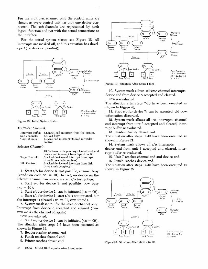
For the multiplex channel, only the control units are shown, as every control unit has only one device connected. The sub-channels are represented by their logical function and not with the actual connections to the interface.
For the initial system status, see Figure 18. All interrupts are masked off, and this situation has developed (no devices operating)
Reader Control
Punch Control
Tape Drives
Printer Control
ucw
Disk Drives
CE = Channel End DE = Device End B = Busy
Figure 18. Initial System Status
Multiplex Channel: Interrupt buffer: Sub-channels: Control units:
Selector Channel:
Channel end interrupt from the printer. UCW3 busy. Device end interrupt stacked in reader control.
U CW busy with pending channel end and device end interrupt from tape drive 5.
Tape Control: Stacked device end interrupt from tape drive 6 (rewind complete) .
File Control: Stacked device end interrupt from disk drive (seek complete).
1. Start I/O for device 6: not possible, channel busy (condition code,ee = 10). In fact, no device on the selector channel can accept a start I/O instruction.
2. Start I/O for device 3: not possible, uew busy (ee = 10).
3. Start I/O for device 2: can be initiated (ee = (0). 4. Start I/O for device 1: start I/O is not initiated, but
the interrupt is cleared (ee = 01, esw stored). 5. System mask set to 1 for the selector channel only:
Interrupt from device 5 accepted and cleared (new psw masks the channel off again).
uew re-evaluated. 6. Start I/O for device 1: can be initiated (ee = ()()).
The situation after steps 1-6 have been executed as shown in Figure 19.
7. Reader reaches channel end. 8. Punch reaches channel end. 9. Printer reaches device end.
48 12-65 Model 40 Comprehensive Introduction
Reader Control
4
Punch Control
Tape Drives
Printer Control
Disk Drives
Figure 19. Situation After Steps 1 to 6
ucw
I/O Interrupt
Selector Channel
Op = Operating CE = Channel End DE = Device End B = Busy
10. System mask allows selector channel interrupts: device end from device 8 accepted and cleared.
uew re-evaluated. The situation after steps 7-10 have been executed as shown in Figure 20.
11. Start I/O for device 7: can be executed, old uew information discarded.
12. System mask allows all I/O interrupts: channel end interrupt from unit 3 accepted and cleared, interrupt buffer re-evaluated.
13. Reader reaches device end. The situation after steps 11-13 have been executed as shown in Figure 21.
14. System mask allows all I/O interrupts: device end from unit 3 accepted and cleared, interrupt buffer re-evaluated.
15. Unit 7 reaches channel end and device end. 16. Punch reaches device end.
The situation after steps 14-16 have been executed as shown in Figure 22.
Reader Control
4
Punch Control
Tape Drives
Printer Control
Disk Drives
Figure 20. Situation After Steps 7 to 10
ucw
I/O Interrupt
Selector Channel
CE = Channel EnG DE = Device End B = Busy

Reader Control
Punch Control
Tape Drives
Printer Control
Disk Drives
Figure 21. Situation After Steps 11 to 13
Reader Control
4
Punch Control
Tape Drives
Printer Control
Disk Drives
Figure 22. Situation After Steps 14 to 16
UCW
UCW
I I
I
I/O Interrupt
B I Selector
Channel
Op = Operating CE = Channel End DE = Device End B = Busy
I/O Interrupt
CE = Channel End DE = Device End B = Busy
17. From this point, no new 1/0 operations are initiated. The system mask is set to allow interrupts from both channels after any interrupt is handled. The remaining interrupts are cleared in the following sequence:
Channel end from the punch. Device end form the punch. Channel end and device end from the reader. Channel end and device end from device 7.
Initial Program Load (lPL)
• IPL is used to start loading the first program into main storage.
• Sets up ccw at MS location o. • Reads double word into MS location 0 from 1/0
addressed by IPL.
• Double word becomes first psw.
Initial program load (IPL) is used to start loading of the first program into main storage.
After the load button has been pressed, the following actions occur:
1. A ccw is generated in location 0 of main storage which specifies the command: Read, command chaining, data address = 0, count = 24.
2. Initiates a start 110 instruction on the device addressed by the load unit switches. This may be any type of device. To illustrate the principle, the device is assumed, in this description, to be a card reader.
3. Execution of this start 110 instruction results in the first 24 columns of the first card being read into main storage, starting at location O. The information punched into this card must be:
Columns 1-8: the first PSW to be used after IPL is completed. Columns 9-16: the second CCW of the IPL command chain. Columns 17-24: the third CCW of the IPL command chain.
4. Because the first ccw specifies command chaining, the next ccw is fetched from main storage location 0+8 ( card column 9). Further operation is therefore already under control of information just read in.
lt depends now entirely on the programmer how his first program is read in. He may choose to read the complete program with a single ccw chain (one ccw required to read one card) which he builds up with the following cards, or he may choose to store first a proper load program which in tum loads the problem program.
5. In any case, IPL is terminated as soon as a ccw no longer specifies command chaining. The psw that is stored at location 0 of main storage is loaded into the data How. The overall system status is as specified in this psw and the first instruction is fetched from the location indicated by IC.
Multiprogramming
• During execution of a single program on any computer, the internal processing capacity is not economically used.
• For a single program, not all 110 devices installed are normally required by the program.
• Efficiency of a system can be increased by running more than one program in parallel.
On any computer, the internal processing speed is normally considerably higher than the speed of 1/0
units where external documents have to be handled. Particularly in commercial applications, the ratio of internal processing and 1/0 operations is such that the CPU has almost constantly to wait until the 110 units are ready to send or accept data.
System Controls 12-65 49

Many jobs in a typical installation use only part of all I/O devices installed and the complete system is used for only a few jobs.
Over-all, the processing capacity of the complete system is normally not very economically used.
Efficiency of any system can be increased if at any time as many functional units as possible are working. This can be achieved by running more than one program in parallel.
This practice is referred to as multiprogramming.
Example: Refer to the sample system configuration in Figure 15. Assume that at a certain time the main job is a billing application for delivered products. The program uses the following I/O units:
3 disk drives containing customer and product records. 1 tape drive with delivery data. 1 printer to prepare the invoices.
The customer and product records are updated accordingly.
In this example, the printer is the slowest functional unit. No matter how high the internal processing speed or the speed of tapes and disks, the rest of the system has almost constantly to wait for the printer.
If, in this installation, other jobs are pending which need I/O devices not already used or which can be shared with the main job (disks), it is sensible to run these jobs in parallel with the main job.
Examples of other jobs possible are: tape sort (four drives available) and card to disk (or vice versa). A further program that may be permanently held in the system would provide for inquiries from the console printer concerning file data.
The time required for one particular job will be increased but, more importantly, the "throughput" will be much higher. (Throughput = number of jobs completed per unit of time. )
System/360 Concept
• System/360 features that simplify multiprogram-ming:
1. Optional high main storage capacities 2. Re-locatable programs 3. Programmed status switching 4. Interrupt system 5. Storage protect feature 6. Interval timer
• A complex operating system is an integral part of the system configuration.
Multiprogramming is basically possible on any computer although the programming effort involved is, in most cases, prohibitive. The system concept of the System/360, however, is based on multiprogram oper-
50 12-65 Model 40 Comprehensive Introduction
ation and provides features that simplify the programming concerned.
High Main Storage Capacity
All processors of System/360 are available with relatively high storage capacities compared with the internal processing capabilities. The IBM 2040 is available with up to 256K bytes of main storage.
Relocation of Programs
Every main storage address is specified by a displacement and the contents of a base register. A program assembled and stored in a certain main storage area can easily be moved to another area of storage by simply changing the contents of the base register. All future references to storage are in the same relation to the base address.
A specific program therefore may use at one time storage locations 1000-7000, and at another time locations 69500-75500, depending on the other programs concurrently executed.
Programmed Status Switching
The status of every program is defined by the psw. Switching from one program to another can be accomplished at any time by replacing the current psw with the psw of the new program. The old program can be continued later at exactly the point and the status at which it was left.
Interrupt System
Asynchronous conditions are signaled to the program at the time they occur (I/O termination). Once such operations are initiated, the individual problem program can ignore them, and if the termination of such operations is essential to carry on, can tum control over to another program that can process data during the dead time of the first program.
If the interrupt caused by termination of the I/O operation comes in, the second program is abandoned, and control returned to the original program.
This switching from program to program at interrupt time can obviously be done between more than just the two programs mentioned.
Storage Protect
Storage protect is a special feature available on the IBM 2040.
The storage protect feature protects the contents of certain areas of storage from destruction due to erroneous storing of information during the execution of other programs.
Protection is achieved by identifying blocks of storage with a storage key and comparing this key with a protection key supplied with the data to be stored.

The detection of a mis-match results in a protection interrupt.
For protection purposes, main storage is divided into blocks of 2,048 bytes. A four-bit storage key is associated with each block. When data are stored in a storage block, the storage key is compared with the protection key. When storing is specified by an instruction, the protection key of the current psw is used as the comparand. When storing is specified by a channel operation, a protection key supplied by the channel is used as the comparand. The keys are said to match when they are equal or when the protection key is zero.
The storage key is not part of the addressable storage. The key is changed by set storage key (SSK) and is inspected by insert storage key (ISK). The protection key in the psw occupies bits 8-11 of that control word. The protection key of a channel is recorded in bits 0-3 of the CAW.
When a protection mismatch due to an instruction is detected, the execution of this instruction is suppressed or terminated, and the program execution is altered by an interrupt. The protected storage location always remains unchanged.
Protection mismatch due to an 110 operation causes the data transmission to be terminated in such a way that the protected storage location remains unchanged. The mismatch is indicated in the csw stored as a result of the operation.
Interval Timer
The timer is provided as an interval timer and may be programmed to maintain the time of day. The timer consists of a full word in main storage location 50 hex. The timer word is counted down under control of the line frequency. The timer word is treated as a signed integer following the rules of fixed-point arithmetic.
An external interrupt condition is signaled when the value of the timer word goes from positive to negative. The full cycle time of the timer is 15.5 hours.
An updated timer value is available at the end of each instruction execution, but is not updated in the stopped state. The timer is changed by addressing storage location 50 hex.
As an interval timer, the timer is used to measure elapsed time over relatively short intervals. It can be set to any value at any time.
In multiprogramming, the timer may be used to measure the time consumed by the individual jobs ( billing) or to prevent a program from monopolizing the CPU (if one of the jobs is program testing for example, where a program error may cause an indefinite loop).
Operating System Principles
• The operating system (os) is a supervisor program that controls the problem programs of the customer.
• The operating system is tailored to the individual system.
• Operating system programs for real-time computers are very sophisticated.
Because of the wide variety of possible System/360 configurations, the operating systems are more or less tailored to the individual system and to the customers' need (multiprogramming, real time, etc.).
On smaller systems, the optional features, interval timer and storage protect, would also affect the operating system. It is obvious that an IBM 2040 with 16K main storage cannot store or use a supervisory system that uses 30K locations.
It is assumed that all os programs are permanently stored within the physical system, e.g. one tape unit with the system tape or part of a disk file has no other function than to be part of the operating system.
The programmed portion of the as is sub-divided into five parts with distinct functions as follows:
Supervisor System
The supervisor system is that part of the system which exercises supervision over the other parts and maintains status records and operating statistics. Supervision is the combined function of allocating, scheduling, dispatching and execution of jobs, including readying jobs for execution and maintaining records of machine, system, and job status together with operating statistics.
Supervision can therefore be defined as the set of control functions exercised by the system and the record-keeping associated with these functions.
Allocation is the action of assigning a machine facility for some purpose, such as assignment of an area of main storage to hold a certain program, or a given tape drive to hold a certain tape file.
Scheduling is the process of ordering future events ( jobs), e.g. determining in which order and at what times they will take place. Jobs are defined and initiated by the user by means of job decks. Jobs may be run in any order or combination, except for orders based on job priorities.
Dispatching is the act of causing events actually to occur according to the schedule.
Load programs and housekeeping programs for the system file and programs for the interface operatormachine are also included in the supervisor system. These programs are commonly referred to as supervisor or monitor programs.
System Controls 12-65 51

Input/Output Control System (I0CS)
The inputloutput control system is that part of the system concerned with the use of the various input! output elements. It contains the actual routines for 110 operations.
The problem programmer specifies 110 instructions in symbolic form which are translated into supervisor calls by the assembly routines. The execution of these instructions is under control of the operating system.
The supervisory program tells the lOCS what physical units are concerned and what operation has to take place. The IOCS in tum executes and controls the operation (error routine) and, upon termination, hands control back to the supervisor.
"Debugging" System
The "debugging" system comprises those parts of the system that assist programming in the location of malfunctions in any part of the operating system. Programs in this section are:
1. Routines for handling program interrupts (program errors)
2. Routines for handling machine check interrupts ( machine errors)
3. The diagnostic monitor
4. Diagnostic programs
System Processors
The system processors are those programs residing in the system library which are used by the system to execute certain standard jobs. Typical of these are the autocoder assembler, FORTRAN assembler, COBOL assembler, sort programs, etc.
Problem Program library
The problem program library consists of all customer programs for the particular system.
Error Detection and Handling
• The system is kept running as long as possible.
• If possible, programmed recovery is attempted.
• Distinction is made between machine and program errors.
• Machine malfunctions in one unit may not cause errors in another unit.
The fundamental operating characteristic of a Systeml 360 is its continuously operating state. During normal system operation the system should never be stopped. Error detection, therefore, may not stop the system if programmed recovery is possible.
52 12-65 Model 40 Comprehensive Introduction
In System/360, distinction is made between machine malfunctions and programming errors. Program errors may not cause indication of machine malfunctions.
Machine Malfunctions
The IBM 2040 is comprehensively checked by redundancy checking, consisting mainly of parity check circuits. All data transfers between functional units are checked by byte. The control circuits are also checked.
If the system is in normal processing mode and a machine check is detected, the machine is frozen at the end of the internal cycle and the complete error environment is stored in coded form into main storage.
This operation is called log out and provides a powerful tool for customer engineering, as the status of all important functional units and information about the program conditions at the time of error are recorded for future investigation.
After the log out is executed, an internal checkout routine applies a check to all functional units. A machine malfunction during this test will stop the system and customer engineer intervention is necessary. If, however, this checkout does not show any machine malfunctions, it is assumed that the original error is no longer present (intermittent failure) and that system operation can be resumed.
The system is then reset and a machine check interrupt is taken. Error data can be analyzed by program and either a re-try of the failing instruction or a branch to the last program check point can be intiated.
Machine errors detected in an 110 unit cannot cause errors in the CPU and vice versa. By design, the data sent across the interface are always in good parity. Control checks detected in 110 units are sent to the CPU as status information. By programming it is possible to obtain more detailed information about 1/0
unit conditions (sense command).
Programming Errors
Programming errors detected by the CPU lead to a program check interrupt. Reasons for program checks are listed in the «Interrupt System," section.
Program checks normally occur during program testing only. The program check interrupt routine indicates to the programmer what condition occurred but abandons the program.
Program checks during actual operation will indicate that certain specifications were not considered (length of result ,fields or tables that now exceed the available storage size). The program will again be abandoned with the proper indication to the operator.
In multiprogram mode, the remaining programs are carried on immediately.

• To the programmer, all processors within System/360 look the same; internal circuitry, however, may be entirely different.
Figure 23 shows a simplified data How of the IBM 2040. Any processor within the System/360 line has the same architecture, i.e., the internal language, the interpretation of instructions and its basic building blocks as seen by the programmer are identical. See detail A of Figure 23.
To the programmer, the various models differ only in storage and channel capacities and in the internal processing speed.
These differences affect the actual circuitry as every model of the line should be the most efficient implementation of its specifications. The IBM 2040 processor is a microprogram-controlled computer, using SLT (solid logic technology) components. The data How is explained in more detail in the following sections.
Main Registers and 16-8it Data flow
• Five main data registers are provided, each two bytes wide, interconnected by a 16-bit data path.
Figure 24 illustrates the basic components of the 2040 CPU. There are five registers, each two bytes wide. A byte is eight bits plus one parity bit, and is the fundamental unit of data in the System/360. The A, C, and R registers have extender bits in the high-order positions. The use of the extender bits is explained in the "Main Storage" section. In general, data transfers are 16 data bits plus 2 parity bits in parallel.
Hereafter, mention will be made only of data bits in transfers; parity is assumed as one extra bit per byte. Each register, may transfer its contents to any of the others via the R register, or back to itself, in one machine cycle.
ALU and 8-Bit Data flow
• Basic registers are connected to the ALU by an in-dependent 8-bit data path.
• ALU processes one data byte at a time.
• P and Q are input registers for ALU.
To enable arithmetic and logical operations to be performed on the data in the registers, the arithmetic
Basic Data Paths
and logic unit (ALU) is added to the data How. See Figure 25. The ALU has two inputs, P and Q, each 8 bits wide plus a parity bit.
Arithmetic and logical operations are performed on one byte at a time. To interconnect the ALU and registers an 8-bit data bus is provided, as in Figure 25. Data on the bus can be selected from, or directed to, either the low- or high-order byte position of the register concerned.
For example, to add the contents of Band D and store the result in D, the low-order bytes from Band D would be fed to the P and Q inputs, respectively, and the ALU output gated back to the low-order position of D. The same operation would then be performed on the high-order bytes, any carry from the low-order addition being added in for the final cycle.
Staticizer Latches (Stats)
• Staticizer latches are multipurpose latches to indicate various machine conditions.
• Some stats are connected to the 8-bit ALU data bus.
In Figure 26, the staticizer latches (stats) are added. They may be set to indicate a machine status such as condition code. Other uses of these stats are as an intermediate temporary storage, to alter control functions, or to extend the number of controls possible with a given set of lines.
In the broadest sense, although the stats may have names denoting their primary functions, they may be regarded as a set of general purpose latches. Thus, a stat may be set to indicate that some condition has arisen, and the microprogram can test for the condition, branch to an appropriate routine, and reset the stat that originally indicated it.
A group of eight stats is connected to the ALU data bus. This gives the possibility of handling control information with all the facilities available for data.
Local Storage and Addressing
• Local storage is a high-speed core storage with a capacity of 144 22-bit locations, operating in splitcycle mode.
• Local storage contains several control and working areas and is the physical location of the 16 general and 4 floating-point registers.
Basic Data Paths 12-65 53

CHANNELS
Selector Channel 1
Interface
Interface ... Mpx Register ~ From C Register
_ Multiplex Cha~el _ r --I Detail A
I I I I I I I
16 General Registers I I
80 4 Floating
Point Registers
I L
Problem Programmers Dataflow /360 -40
Figure 23. 2040 Simplified Data Flow
I --1
CPU
-t
C) c: VI VI Qj
Main Storage
-u ""OI-------f «
Mpx Store
R Register
144 Words 22 Bits Each
Staticizer Latches
I I
L ..sd.. ..chaorW ...J
Control CPU & Channel Data Flow

Figure 24. Main Registers and l6-bit Data Flow
Figure 25. ALU and 8-Bit Data Flow Added
Figure 26. Staticizer Latches Added
Staticizer latches
§
• The R register is the data register of local storage.
• LSAR is the address register of local storage.
• The local storage address loop is connected to the R register data bus via Hand J registers.
The local storage (LS) is a high-speed core storage with a capacity of 144 22-bit locations. LS read and write cycles may be run independently (split-cycle mode), each cycle (read or write) being 625 nanoseconds, which is the basic CPU timing cycle.
For high-speed access to several locations in sequence, LS would be cycled using continuous read calls and the contents of the accessed locations transferred each cycle to the required destination.
LS is used as a general-purpose, high-speed intermediate storage. It also has locations reserved for specific functions. Thus, the general and Boating-point registers "seen" by the problem programmer are locations in LS. Additional uses include channel control, working space, psw storage, and dump areas for use during microprogram interrupts.
The LS data register is the R register which is connected to the other main data Bow registers. Figure 27 illustrates the addition to the data Bow of LS and its addressing circuits.
$taticizer La
Figure 27. Local Storage Added
The local storage address register (LSAR), the incrementer, and registers Hand J form the address loop. The incrementer can alter the LS address by ± 1, - 2, or O. LSAR contents are routed through the incrementer to H or J. The purpose of Hand J is to hold LS addresses for subsequent use in LSAR.
LSAR is loaded at the beginning of the machine cycle, Hand J at the end. Thus, an address can be set into LSAR at the start of a cycle, used to call LS,
transferred to H or J via the incrementer at the end of that cycle, and transferred back to LSAR for use at the beginning of the next cycle, and so on.
The LS address loop bus is 8 bits plus one parity bit wide. Data may be loaded into the LS address loop registers from the machine data Bow and also from entry switches on the console.
Main Storage (NlS)
• Main storage is a core storage with a capacity of up to 256K bytes (128K halfwords). It operates in split-cycle mode with a total cycle time of 2.5 microseconds.
Basic Data Paths 12-65 55

• Main storage always reads or writes one halfword (two bytes) at a time.
• ~fain storage data register is the D register.
• Main storage address registers are the A or S registers.
• ~fain storage is addressed with binary addresses up to 18 bits.
• With a special address bit (stat Yl.), a special area, called multiplex storage, can be addressed.
Figure 28 shows the addition of main storage to the data flow. The addition of a main storage array to the data flow provides an immediate-access bulk store which can be used to hold program instructions and data. The main storage (MS) in the 2040 may have a capacity of 16, 32, 64, 128, 192, or 256 K bytes.
Main Storage
Mpx Store
144 Words 22 Bits Each
Figure 28. ~Iain Storage and 16-Bit Buses Added
Staticizer Lat
MS always reads or writes two bytes at a time and operates in split-cycle mode. The time for one complete cycle, read and write, is 2.5 microseconds, or 4 times the basic machine cycle of 625 nanoseconds. This means that MS access can take place once every four machine cycles.
Data Transfers
Figure 28 shows that MS data are transferred via a 16-bit bus to register D, whose special purpose is to act
56 1-69 Model 40 Comprehensive Introduction
as the main storage data register. All data in and out of the array are routed via register D and the 16-bit bus.
Addressing
The MS address circuits are fed by register A (or S for selector channel), whose special purpose is to act as the main storage address register. These registers are connected to the MS address decoders via the address bus. The A register content is decoded as a binary number.
The various storage capacities are defined by the number of bits contained in the address. A capacity of 128K bytes actually means that the storage is addressed with 17 bits and has a total number of 131,072 storage locations. Data are stored in :\IS in halfwords, or 16 bits plus 2 bits parity. The j\IS is thus said to be 16 bits wide. Every access to :\IS results in 16 + 2P bits being set into or stored from D. The lowest-order bit in the :\IS address in A denotes the byte concerned. The actual address lines do not use this low-order bit which is reserved for byte selection only.
Extended Addressing
Seventeen binary lines are needed to address 128K bytes of storage, and 18 binary lines are needed for 192K and 256K. To accommodate the extra address bits, the A, C, and R registers have extenders (3 bits plus parity) called AX, ex, and RX, respectively. The A register (Figure 28) needs the extender because it addresses main storage. The C register needs the extender because it receives updated addresses from ALU, and the R register because it transfers addresses between the C and A registers.
Special Area
At this point, main storage, with address and data registers and buses, has been added to the data flow. In addition, there is a special multiplex storage area in :\IS. This comprises additional locations which can be accessed only for multiplex channel operations when a stat called Yl is set (this stat serves as an additional address bit for MS addressing).
The special area contains one uew (unit control word, 10 bytes) for every multiplex subchannel and contains the necessary control information to sustain the operation of a subchannel.
Control
• Transformer read only storage (TROS) stores the microprogram that controls the data flow.
• TROS can be addressed with information coming from the data How.

g> Main ";;; Ql Storage -ot------I ~ Mpx Storage
Figure 29. The Read Only Storage Added
Staticizer Latches
§
Control CPU & Channel Data Flow
Control of the data flow (Figure 29) is accomplished by a microprogram in TROS, and logic circuits such as controllines, control latches, and stats.
Channels
• Channels provide the data path and control between main storage and 110 devices.
• The entire CPU data How may be used as a channel.
• CPU and channel operations cannot be executed simultaneously.
The basic function of a channel is to provide the data path for 110 information between main storage and 110 device. The channel also controls the information transfer. A channel is an independent computer for 110 operations.
Some hardware is added to the basic CPU to perform the channel functions with the original computer. Separate microprograms (channel programs) control the entire operation, which may include data handling within the CPU and control of the 110 device via the interface.
It is obvious that this design provides either a CPU
or a Channel and the two units cannot operate simultaneously. However, CPU and channel operations are interleaved to give the most efficient over-all performance. The time used to read a record from tape from the start 110 instruction until the record is available in main storage, is split up into CPU and channel time and most of this time will be available for the CPU.
Multiplex
• The only special hardware for the multiplex (MPX)
channel is the circuitry required to communicate with the interface and the special MPX storage area in main storage.
• Any microprogram interrupt by the multiplex channel dumps the cpu.
The multiplex channel has no special data flow circuits except those necessary in connection with the standard interface.
The R bus is gated from the interface line terminators for read data, the low-order byte of register C is gated to the interface line drivers for write data.
Special channel-control circuitry includes main storage, MPX storage, and the logic for generating and . analyzing interface control signals.
For any microprogram interrupt, the CPU has to be "dumped" (data flow contents preserved in local storage for later retrieval) in order to have the entire data flow available as channel.
Example: To accept one byte of read data from the interface, the following sequence will take place:
1. A device on a mpx subchannel is ready to send one byte of data and requests a microprogram interrupt.
2. The data flow, which is currently used as CPU,
is dumped into local storage leaving the data flow path available to the mpx channel.
3. The channel function now taking place includes: a. Identifying the device b. Fetching necessary control information from
mpx storage c. Accepting the data byte from the interface and
gating it to the D register and to main storage d. Updating mpx storage
4. U ndump (i.e. retrieve the original data flow from local storage) and continue CPU processing.
On burst mode operations on the mpx channel, the CPU is monopolized for the entire 110 sequence; therefore, no CPU processing time is available for the duration of the data transfer.
Selector Channel
• Only D register has to be dumped.
• A five-byte data-buHer is provided between inter-face and channel.
• Independent MS address register is S register.
• TROS is addressed by independent ROSCAR.
• T register and other registers are provided for con-trol information.
In addition to the circuitry required to communicate with the standard interface, the selector channels (Figure 23) contain a five-byte data-buffer and reg-
Basic Data Paths 12-65 57

isters for control information (ucw information). These facilities make the selector channels almost independent of the CPU hardware.
Only the MS access path is shared with the CPU
(D register). Therefore, the CPU content of the D register has to be preserved during channel operations.
The two main CPU units which are duplicated in the channel are:
1. An additional main storage address register (S register ).
2. An additional TROS address register (ROSCAR, TROS
channel address register). With this independent hardware, channel interference with the CPU is kept to a minimum.
58 12-65 Model 40 Comprehensive Introduction
During data transmission, the CPU program is only halted for the transfer between main storage and buffer.
Example: To accept read data from the interface, the following sequence will take place:
1. Data transfer between interface and buffer is completely independent of CPU operation.
2. \iVhenever two bytes of data are available in the buffer, the CPU operation is halted and control is switched from ROAR to ROSCAR.
3. The channel preserves the D register contents and directs the buffer contents to main storage.
4. D register is restored and control is handed back to ROAR.

CPU Timing
• Basic machine cycle is 625 nanoseconds divided into overlapping timing pulses of equal length.
• One set of timing pulses is continuously available (P pulses); a second identical set only for the cycles in which microinstructions are to be executed (T pulses).
The basic machine cycle of 625 nanoseconds (1 nanosecond = 10-9 seconds) is split into eight overlapping timing pulses of equal length, time 1 to time 4 delayed (del).
One continuously available set of pulses is called P pulses (PI to P4 del). A second identical set is generated whenever microinstructions are to be executed. This set is called T pulses (Tl to T4 del). T pulses are developed by gating P pulses. The only time when T pulses are blocked is during "hardware" cycle and in "hardstop."
Some basic data-How timings are shown in Figure' 30. LSAR, P and Q are set early in the cycle. A, B, C, and D are set late in the cycle.
Local storage is called early; LS data are available or have to be in the R register in the first half of the cycle. The ALU output is available late in the cycle.
According to these timings within the machine cycle, the following data transfers are possible in one cycle:
1. On the 16-bit path: a. Transfer from one register (A, B, C, and D)
to any other (via R), or
Basic System Timing
b. Transfer between a register (A, B, C, and D) and local storage (via R).
2. On the 8-bit ALU data path: a. Transfers from registers (A, B, C, and D) to
ALU registers P and Q and b. Performing the ALU function, and c. Gating the ALU output to a register (A, B, C,
and D). Operations on the two data buses (R register and ALU) can occur simultaneously.
CPU and MS Timing
• The basic main storage cycle is 2.5 microseconds.
• To complete one main storage cycle, 4 machine cycles are necessary.
• Between main storage read and write half cycle an unspecified number of machine cycles may take place.
The basic main storage cycle is 2.5 microseconds split in two halves for read and write. In order to complete one main storage cycle, four machine cycles are necessary (example: read out information and restore the location).
Between the read and write cycle of main storage an unspecified number of machine cycles may take place (zero up to any number).
Figure 30 shows the relationship between main storage and CPU timing.
Basic Systems Timing 12-65 59
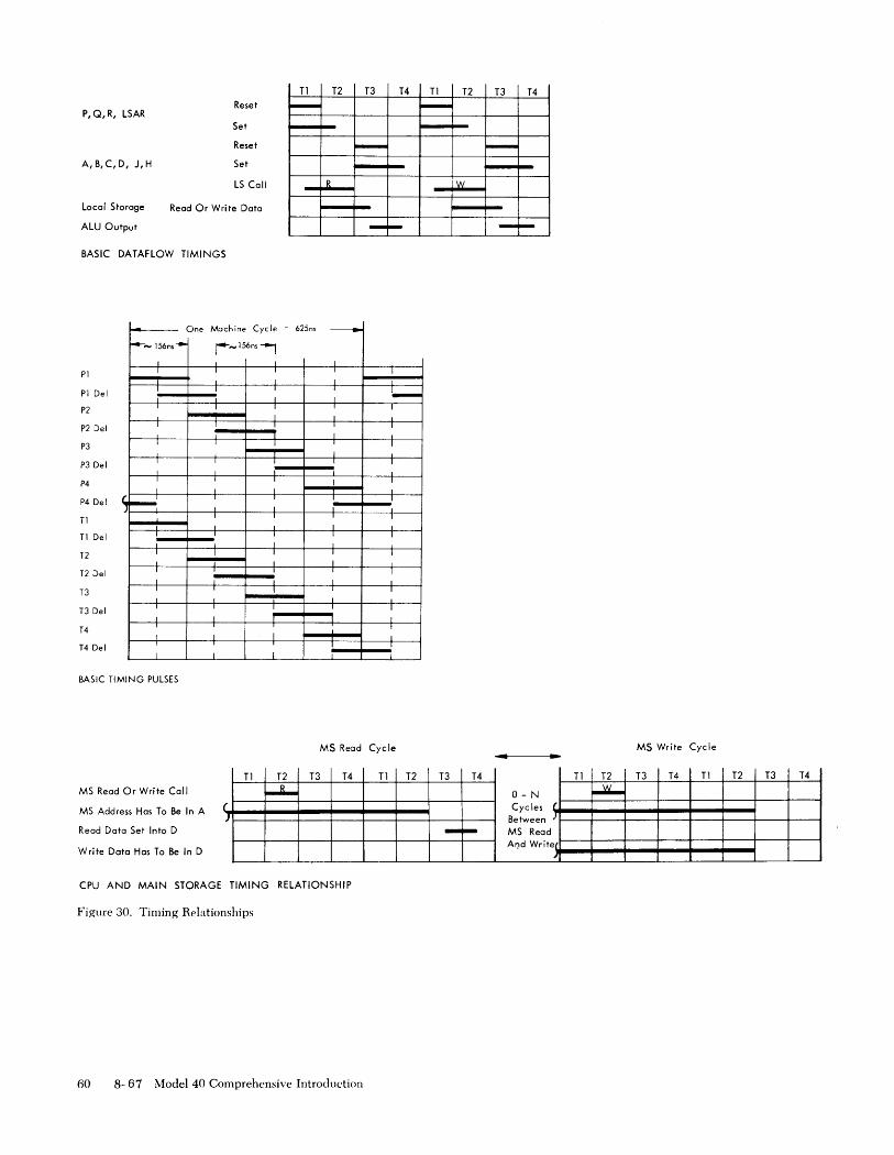
Reset P,Q,R, LSAR
Set
Reset
A,B,C,D, J,H Set
LS Call
Local Storage Read Or Write Data
ALU Output
BASIC DATAFLOW TIMINGS
Pl
Pl Del
P2
P2 Del
P3
P3 Del
P4
P4 Del
Tl
Tl Del
T2
T2 Del
T3
T3 Del
T4
T4 Del
One
,--- 156ns--
I I
I
I
I
I
I
I I
I ,-I
I
I I
I I
I
I
I
BASIC TIMING PULSES
Machine Cycle
r-..... l56ns i I
I I
I I T
I I 1
I I- I
I
I I I
I
I I I I
I I I I
I T I I
I
I
I I
I I
Tl T2 T3 T4 Tl T2
~ ,........
~
R W
--
= 625ns -----I I I I
I !.o-I
I I I
I
I I I 1
I I
I I
I T I I I
I I I I I I
I
I I I
I I
I I
MS Read Cycle
Tl T2 T3 T4 Tl T2 T3 T4
MS Read Or Write Call ~ (
J MS Address Has To Be In A
Read Data Set Into D --Write Data Has To Be In D
CPU AND MAIN STORAGE TIMING RELATIONSHIP
Figure 30. Timing Relationships
60 8- 67 Model 40 Comprehensive Introduction
T3 T4
-
- ~
MS Write Cycle
Tl T2 T3 T4 Tl T2 T3 T4
O-N ~
Cycles (
Between J
MS Read AQd Writer ,
A single step of a microroutine is called a microinstruction. A microinstruction is very similar to a machine-language instruction. Microinstructions can test conditions and branch, move data,~ and set and reset STATS.
Before the IBM System/360, electronic circuits controlled the functions of the computer. Once the operation code was analyzed, special circuits were activated for every microstep, and sequencing and control functions required special circuits for almost every machinelanguage instruction.
In the IBM 2040 processor, the standard data How circuits are controlled by stored program routines held in transformer read only storage (TROS).
The IBM 2040 can be considered as a group of general purpose logic circuits with a microprogram that simulates the IBM System/360 architecture. With a different microprogram, any other computer could be simulated.
Microprogramming Concepts
Two microprograms actually simulate the 1401 and 1410 (special features called 1401/1460 and 1410/7010 compatibility feature).
The capacity of TROS, an inductive type storage, can vary to a maximum of 8,l92 words or microinstructions. TROS contains fixed, predetermined information that can only be read out. The information is printed as drive lines on plastic tapes. These drive lines act as primary windings of coupling transformers for all bit positions where information is desired.
There are two 56-bit words on a tape. The TROS control word always causes the same actions and tests to take place. Variations of a microroutine are possible only by branching to alternate TROS control words. A control word controls the system data How, controls special circuits, determines the next TROS address, and parity-checks itself.
Microprogramming Concepts 12-65 61
Index
Address Generation base address displacement index ...
Basic data paths ALU ...... . main registers staticizer latches ......... .
Binary fixed-point arithmetic add and subtract divide multiply
Branch instructions branch and link branch on condition branch on count .. condition code
Channel address word command word control .. multiplex operation program ....... . selector .... . status ..... . status word format
Channel data paths Coding
binary .. . data .... .
23 23 23
53 53 53
16 17 17
28 28 28 28
40 40 41 37 38 38 38 42 42 57
11 . . . . . . . . . 10
decimal hexadecimal
. . . . . . . . . . . . . . . . 10
Configuration Control storage CPU status
masked or interruptible ....... . running or waiting stopped or operating ........... . supervisor or problem
. . . . . . . . 10 .... 35,36
56
35 34 34 35
Data flow .. . . . . . . . . . . . . . . . .. . ....... . 54 24 20 10
Data-handling instructions .... . ........ . Decimal arithmetic Decimal coding Error detection
machine malfunctions programming errors ..
Floating-point arithmetic add and subtract divide ....... . examples multiply notation ..
Functional units Hexadecimal coding
I/O device addressing I/ 0 instructions
halt I/O ......... . start I/O test channel
62 12-65 Model 40 Comprehensive Introduction
52 52
18 18 19 18 18 9
10 39
44 43 44
test I/O I/O interrupts
attention channel end clearing control unit end device end examples generation and stacking handling .. program control sequencing .
I/O operations control data transfer test ...
Initial program load ....... . Instruction format ......... . Instruction length code Instruction types
branch instructions ............. . commercial instruction set data-handling instructions logical instructions scientific instruction set standard instruction set ....... . status switching instructions universal instruction set
Interrupt code Interrupt types
I/O interrupts Interrupts
external I/O machine-check program-check supervisor-call ..
Local storage Logical instructions Main storage
addressing data transfers
Masking of interrupts Microprogramming concepts Multiplex channel Multiprogramming Operating system
I/O control system supervisor system
Permanent storage assignments Priority of interrupts ....... . Program status word PSW Bits
AMWP condition code instruction counter
Selector channel Standard interface System timing
Timing - Basic system ...
44
45 45 46 45 45 48 45 47 45 47
37 37 37 49 22 34
27 24 24 27 24 24 30 24 33 33 45
31 31 31 31 31 53 27
56 56 32 60 37 49
52 51 32 32 29
30 30 30 38 36 59
59

System/360 Model 40 Comprehensive Introduction FETOM
READER'S COMMENT FORM
• How did you use this publication?
D As a reference source D As a classroom text D As a self-study text
We would appreciate your comments; please give section or figure titles where appropriate.
• What sections or figures were particularly useful or understandable to you?
• What sections or figures could be improved? How?
• What sections or figures require additional information?
• Any other comments?
• How do you rate this manual?
If you desire a reply by the group that prepared this manual, include your name and address.
Thank you for your cooperation. WTC users must add postage.
SY22-2840-2

YOUR COMMENTS, PLEASE . ......... .
Your answers to the questions on the back of this form, together with your comments, will help us produce better publications for your use. Each reply will be carefully reviewed by the persons responsible for writing and publishing this material. All comments and suggestions become the property of IBM.
Note: Please direct any requests for copies of publications, or for assistance in using your IBM system, to your IBM representative or to the IBM branch office serving your locality.
fold fold
() C ~
~ r o Z C)
~ I CJ)
C Z m
............................................................................................................................................................
BUSINESS REPLY MAl L NO POSTAGE STAMP NECESSARY IF MAILED IN THE UNITED STATES
ATTENTION: FE MANUALS, DEPT. B96
fold
POSTAGE WILL BE PAID BY ....... .
IBM CORPORATION P.O. BOX 390 POUGHKEEPSIE, N.Y. 12602
FIRST CLASS PERMIT NO. 419
POUGHKEEPSIE, N.Y.
fold
~ ~
cu u
e r:: >- e ~ ~ cu r:: ~ cu - cu ~ -tIl-..c til >- r:: .0-4 ~ en .; ....:I en
:t CUT HERE
SY22-2840-2
International Business Machines Corporation Data Processing Division 112 East Post Road, White Plains, N. Y. 10601 IUSA OnlY]
IBM World Trade Corporation 821 United Nations Plaza, New York, New York 10017 Ilnternationall
I I I I
--.-J
CJ) '< ~ CD
3 W ~ ~ o c.
~ () o 3 ~ CD =r CD en <' CD
~ o c. c !l o· ::J
" m -I a ~