features • ttl-compatible signal input • single 15v to … rev.: 0/2017 p-1 reerece e r-ref01-hb...
TRANSCRIPT
www.recom-power.com REV.: 0/2017 P-1
Reference Design
R-REF01-HB
Features
Reference Design
DANGER!This board is designed to be used with voltages up to 1kV, only qualified personnel should work with this board. Direct contact with hazardous voltage can cause injury or death!
Never leave the board operating unattended. After removing the high voltage from the board, discharge the capacitors with a suitable discharging resistor to avoid elec-trical shock!
Caution:This reference design is built with ESD (electrostatic discharge) sensitive components. Always follow ESD prevention procedures when handling the product to avoid failures!
• Half-bridge voltage up to 1kV• TTL-compatible signal input• Single 15V to 42V supply• Shoot-through protection• Separate input for low and high-side switch for use with different topologies• Qualified with 65kV/µs @ Vcommon mode =1KV
Description
The Half-Bridge Gate-Drive Power Supply Reference Design (RD) consists of a half-bridge suitable for voltages up to 1kV and a fully-isolated driver stage with isolated power supplies for the low-side and the high-side switching transistors. It is suitable for single gate/drive supply voltages as low as +4V as well as dual gate drive supply voltages as high as +20V / -5V (30V max) with no maximum duty cycle limitations.
Two R12P22005D, R12P21503D, R12P21509D and R12P06S DC/DC modules each are included in the R-REF01-HB design kit.
NOTE: transistors sold separately.
The signal ground is galvanically isolated from the power ground and can be connected to any potential, as long as it is less than 2.5kV with respect to the power potential (high-side and low-side). The limiting element is the gate driver IC specification.
Features: • Optimized for very high switching speed• 2.5kV continuous input to output isolation • High gate-drive currents (up to 10A source and sink)• The RD is fitted with a SI8273 gate driver, but can be used with any pin-compatible gate driver with a PWM input (SI8274) or for gate driver ICs with reinforced isolation, for example the UCC21520 (dual pinout layout on PCB).
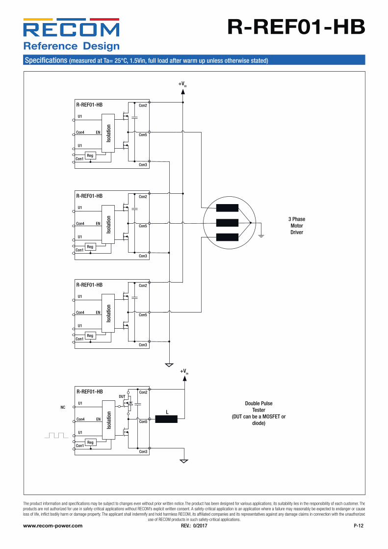
This RD can easily be configured for the following topologies (see application suggestions section):• LLC half-bridge• Asymmetric duty cycle half-bridge (forward and flyback)• Active clamp half-bridge (forward and flyback)• Full-bridge / phase-shifted full-bridge• 3-phase B6 bridge• NPC B6 bridge (additional driving circuit for NPC is required)• Double pulse test• Synchronous boost converter• Synchronous buck converter
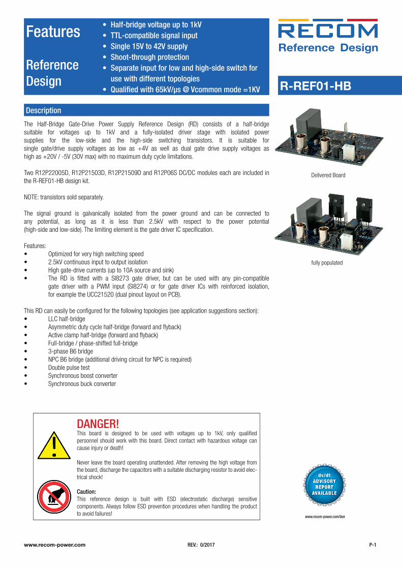
Delivered Board
fully populated
www.recom-power.com/bier

www.recom-power.com REV.: 0/2017 P-2
Reference DesignSpecifications (measured at Ta= 25°C, 1.5Vin, full load after warm up unless otherwise stated)
R-REF01-HB
continued on next page
Component Placement
15V to 42V
CON1
C16FB1
LED3
C5
IC3
LED2
R13
R18
R17
R20
R26R7
FD2
T2
R2IC
5
LED4
R23
C2
IC1
IC7
IC2
C2R6
C4C3R4 R5
LED1
R25
R12
R16
R19
CON5
R15
R24
R1
C18
C19
C15C6
C12C11IC6
R21
T1
R8
C13C14
R3C8
IC4
C9
C7 IC8R22
R10
U1
FD1
CON3
CON2
C12
C17
R11R9U2
D2
D1
R14
CON4
ENABLESignal Low Side
Switch Node
High Side Switch Low Side Switch
Signal High Side
1000V Max
-VBridge
+VB
ridge
TTL-compatible
Input
BASIC CHARACTERISTICSParameter Condition Min. Typ. Max.
Input Voltage Con1 15V 42V
Input Voltage Con2 -> Con3 limited by C10 0V 1000V
Digital U1, U2, Enable -0.5V 5.5V
Logic High Input Threshold 2V
Logic Low Input Threshold 0.8V
Input Hysteresis 350mV 400mV
Maximum Ratings -0.5V 5.5V
Driver Section
Source and Sink Current (max) 10A
Total Drive Voltage positive and negative +4V 30V
Propagation Delay system before gate resistors 20ns 40ns 70ns
Rise and Fall Times refer to the datasheet of the gate-driver IC
Isolation
Isolation Voltage input to output 2.5kVDC

www.recom-power.com REV.: 0/2017 P-3
Reference DesignSpecifications (measured at Ta= 25°C, 1.5Vin, full load after warm up unless otherwise stated)
R-REF01-HB
Following DC/DC models are suitable for use with this reference design
Component List
Part Description
IC2DC/DC isolated converter for high-side gate-driver. Depending on the transistor type, fit the appropriate DC/DC converter (please refer to pages P-10 to P-12).
IC3DC/DC isolated converter for low-side gate-driver. Depending on the transistor type, fit the appropriate DC/DC converter (see table 1).
T1 High-side switching transistor (not supplied). Read important notice below.
T2 Low-side switch transistor (not supplied). Read important notice below.
Note:The transistors are placed on the edge of the PCB so that they are easy to mount to a heatsink. They can also be mounted inverted on the bottom side of the PCB. Both TO247-3L and TO247-4L format transistors can be used by using the appropriate hole set.
CON1 Connector for logic and driver supply. Connect a 15V, 18V, 24V or 36V DC supply here.
CON2 +V bridge voltage: connect a positive voltage up to 1kV in respect to power-GND to this connector.
CON3 -V bridge voltage: power-GND
CON4 Enable: a high signal enables the driver signals. Place the jumper on the connector to enable the signals permanently
CON5 Switching node of the half-bridge
U1 Signal high-side: TTL-compatible input for the high-side transistor
U2 Signal low-side: TTL-compatible input for the low-side transistor
Table 1
Model Power [W] Output Voltage [V] Application
R12P22005D* 2 +20/-5 SiC MOSFETs
R12P21503D* 2 +15/-3 SiC MOSFETs
R12P21509D* 2 +15/-9 IGBTs
R12P1509D 1 +15/-9 IGBTs
R12P06S* 1 +6 GaN
R12P12S 1 +12 Cascode/Si MOSFET
*these models are included in the reference design. Each of them two times
Truth table (with IC1 SI8273 mounted):
Input OutputComment
U1 U2 Enable High-side Gate Low-side Gate
L L H L L
L H H L H
H L H H L
H H H L L Invalid state
X X L L L Device is disabled
www.recom-power.com REV.: 0/2017 P-4
Reference DesignSpecifications (measured at Ta= 25°C, 1.5Vin, full load after warm up unless otherwise stated)
R-REF01-HB
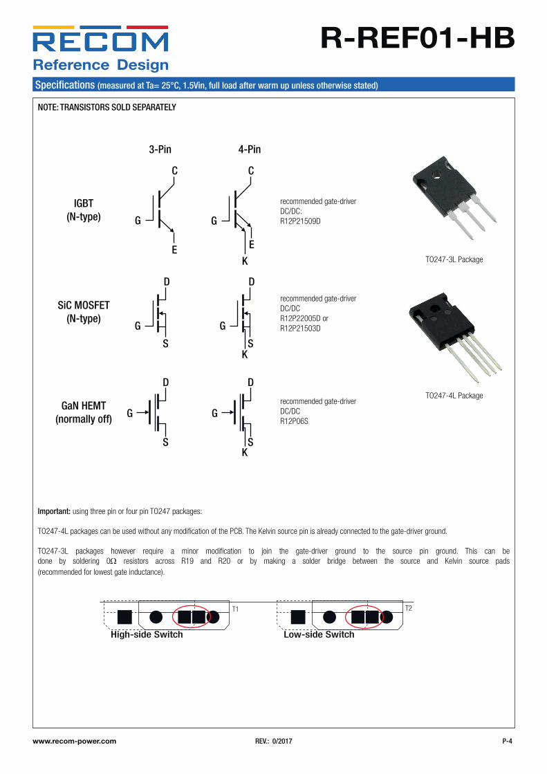
TO247-4L Package
recommended gate-driver DC/DCR12P22005D orR12P21503D
recommended gate-driver DC/DCR12P06S
3-Pin
IGBT(N-type)
SiC MOSFET(N-type)
GaN HEMT(normally off)
C
G
G
D
D
S
S
E
C
GG
E
K
4-Pin
G
D
SK
K
G
D
S
Important: using three pin or four pin TO247 packages:
TO247-4L packages can be used without any modification of the PCB. The Kelvin source pin is already connected to the gate-driver ground.
TO247-3L packages however require a minor modification to join the gate-driver ground to the source pin ground. This can be done by soldering 0Ω resistors across R19 and R20 or by making a solder bridge between the source and Kelvin source pads (recommended for lowest gate inductance).
T2T1
High-side Switch Low-side Switch
NOTE: TRANSISTORS SOLD SEPARATELY
recommended gate-driver DC/DC:R12P21509D
TO247-3L Package

www.recom-power.com REV.: 0/2017 P-5
Reference DesignSpecifications (measured at Ta= 25°C, 1.5Vin, full load after warm up unless otherwise stated)
R-REF01-HB
Schematic
Description:The reference design board requires a single supply voltage with a range of 15-42V. IC5 creates the regulated 12V supply for IC2 and IC3.IC2 generates the isolated high-side gate-driver supply voltage. Choose the appropriate DC/DC converter from the selection provided.IC3 generates the isolated low-side gate-driver supply voltage. Choose the appropriate DC/DC converter from the selection provided.IC8 creates a +Vcc rail required for the gate driver.IC1 isolates the control signals and level shifts the TTL input to the gate-drive voltages.IC7 can be mounted instead of IC1 if reinforced isolation is required.IC4 and IC5 amplify the maximum gate-drive current to ±10A.R24 and R25 are not fitted. Zero Ω resistors can be mounted if IC4 and IC5 are not required (for example GaN transistors).
The input GND1 is galvanically isolated from the high-side GNDA and the low-side GNDB.For single-ended designs, it is recommended to connect GND1 to Power-GND (CON3) with a star-earth configuration. For full-bridge configurations, couple GND1 to Power-GND with Y-Capacitors to avoid generating high potentials caused by common mode currents.
R15, R16, R17 and R18 are not fitted. The positions can be used to add dummy loads for the power supplies if needed, for example, under very light load conditions or low switching frequencies. Alternately R16 and R18 can be used to allow single-output voltage DC/DC converters to be used by connecting -Vout to the gate-driver ground.
Configuration R15, R17 R16, R18
Dual Output DC/DC, Normal Load (standard) Not required Not required
Dual Output DC/DC, Light Load 12kΩ 12kΩSingle Output DC/DC, Normal Load Not required Zero ΩSingle Output DC/DC, Light Load 12kΩ Zero Ω
R1 and R4 control the turn-on slew rate. 22Ω is fitted as standard.R2 and R5 control the turn-off slew rate. 3.3Ω is fitted as standard.These 0207 package resistors are made to withstand highly pulsed loads. Gate currents up to 10A are possible.
GNDI
GNDI
GNDI
GNDIGND
I
GND
B
+12V
+5V
GNDI
GNDI
VDDA
VDDB
+5V
+5V
GNDI
GNDB
DRIVERSOURCE
HS
VDDA
VDDA
DRIVERSOURCE
HS
+5V
GNDA
+12V
VDDB
GNDI
GNDI
GNDI
+12V
GNDI
GNDI
+5V
GNDB
GNDB
VDDA
GNDA
GNDA
GNDA
VDDBVDDB
GNDI
+12V
GNDI
GNDI
GND
A
1
2
3
4
5
6
8
9
10
11
14
15
16
in1
in2
en
out2
out1
VCCI
GND
INA
INB
DISABLE
VCCI
DT
OUTB
VSSB
VDDB
VSSA
OUTA
VDDA
IC7-A UCC21520
4
IC8-B
1
23
4
5
+Vin
-Vin -Vout
Gnd+Vout
IC3 R12Pxx
1 2
R23R302071W
12
R2310K0603100mW
12
R13
10K
0603
100m
W
12 R11
10K 0603100mW
1
2
C191uF16V 0603
12
R19
0R0603100mW
3
4
1
2
5
10
9
11
14
15
16
8
in1
en
VDDB
GNDA
VOA
VDDA
ENABLE
VDDI
GNDI
VIA
VIB
GNDB
VOBVDD2
IC1 Si8273
1
2
C81uF50V 0603
1 2
CON362409-1
21
D2 PMEG6010
1 in2U2-A
BNC
12
R260R0603100mW
1 2R25
0R 0603 100mW
1
2
C181uF25V 0603
21
D1PMEG6010
1 2out2
R32K0 0603100mW
1 2
R53R302071W
1
2
C14100nF50V 0603
1
2
C151uF50V0603
1
23
4
5
+Vin
-Vin -Vout
Gnd+Vout
IC2 R12Pxx
1 2
R122R02071W
12
R810K 0603100mW
1
23
45
D
S
KS
GSG
T1
1
2C13 1uF
50V 0603
12
R910K 0603100mW
12R22
10K 0603100mW
3
2
1
GND
+Vin +Vout
IC8-A L78L05
1 2R24
0R 0603 100mW
12
R20
0R0603100mW
1
2
3
GND
+Vin +Vout
IC5 R-78C12-1.0
1
2
C172.2nF50V 0603
12
LED4
1U1-ABNC
1
2
C122uF25V 1210
12
R1010K 0603100mW
1 2
R4
22R02071W
12
R1410K 0603100mW
1
2
3
4
6
IC4ZXGD3006E6TA
12
R210R0603100mW
12
LED2
1
2
C91uF50V 0603
12
R12
10K
0603
100m
W
12 R16
12K 1206250mW
12
R1812K 1206250mW
1
2
C6100nF50V 0603
1
2
C71uF50V0603
12
R710K 0603100mW
1 2
R62K0 0603100mW
12
LED1
1
2
C2
22uF25V 1210
12 CON5
1
2
C31uF50V 0603
1
2
C101uF1kV
12
CON262409-1
1
2C41uF50V0603
12
R1512K 1206250mW
12
R1712K 1206250mW
1 2
C12100nF 50V 0603
1 2
C111uF50V 0603
1
23
45
D
S
KS
GSG
T2
1
2
3
4
6
IC6ZXGD3006E6TA
1 2
CON461300211121
1
2
C1610uF50V 1210
2
1
CON139-29-0023
12
LED3
1
2
C54.7uF50V 1206
12
FB1
110R 4A 1806
VDDB Supply
5V Supply
12V Supply
VDDA Supply
www.recom-power.com REV.: 0/2017 P-6
Reference DesignSpecifications (measured at Ta= 25°C, 1.5Vin, full load after warm up unless otherwise stated)
R-REF01-HB
15V to 42V
CON1
C16FB1
LED3
C5
IC3
LED2
R13
R18
R17
R20
R26R7
FD2
T2
R2IC
5
LED4
R23
C2
IC1
IC7
IC2
C2R6
C4C3R4 R5
LED1
R25
R12
R16
R19
CON5
R15
R24
R1
C18
C19
C15C6
C12C11IC6
R21
T1
R8
C13C14
R3C8
IC4
C9
C7IC8
R22R10
U1
FD1
CON3
CON2
C12
C17
R11R9U2
D2
D1
R14
CON4
ENABLESignal Low Side
Switch Node
High Side Switch Low Side Switch
Signal High Side
1000V Max
-VBridge
+VB
ridge
TTLCompatible
Input
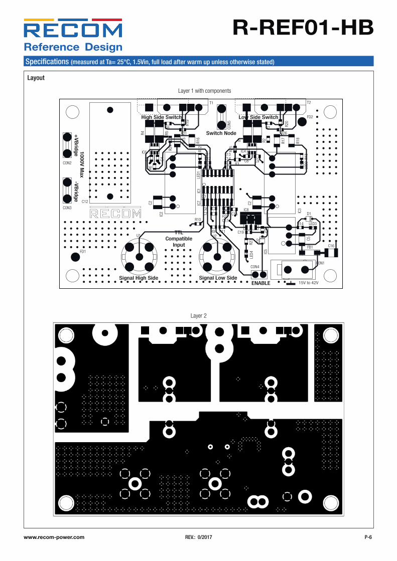
Layout
Layer 1 with components
Layer 2
www.recom-power.com REV.: 0/2017 P-7
Reference DesignSpecifications (measured at Ta= 25°C, 1.5Vin, full load after warm up unless otherwise stated)
R-REF01-HB
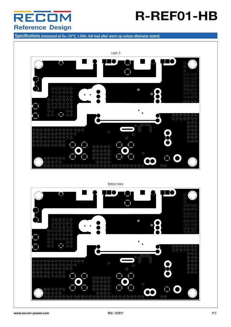
Layer 3
Bottom View
www.recom-power.com REV.: 0/2017 P-8
Reference DesignSpecifications (measured at Ta= 25°C, 1.5Vin, full load after warm up unless otherwise stated)
R-REF01-HB
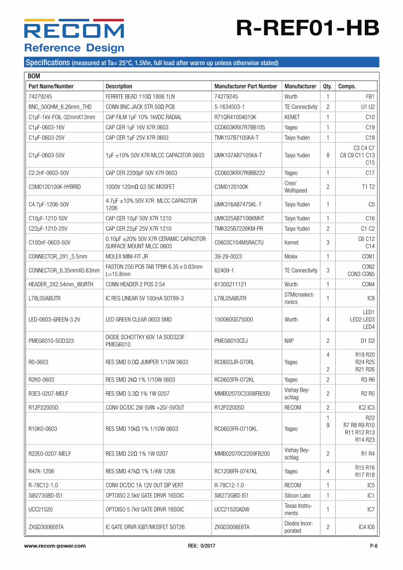
Part Name/Number Description Manufacturer Part Number Manufacturer Qty. Comps.
74279245 FERRITE BEAD 110Ω 1806 1LN 74279245 Wurth 1 FB1
BNC_50OHM_6.26mm_THD CONN BNC JACK STR 50Ω PCB 5-1634503-1 TE Connectivity 2 U1 U2
C1µF-1kV-FOIL-32mmX13mm CAP FILM 1µF 10% 1kVDC RADIAL R71QR41004010K KEMET 1 C10
C1µF-0603-16V CAP CER 1µF 16V X7R 0603 CC0603KRX7R7BB105 Yageo 1 C19
C1µF-0603-25V CAP CER 1µF 25V X7R 0603 TMK107B7105KA-T Taiyo Yuden 1 C18
C1µF-0603-50V 1µF ±10% 50V X7R MLCC CAPACITOR 0603 UMK107AB7105KA-T Taiyo Yuden 8 C3 C4 C7 C8 C9 C11 C13
C15
C2.2nF-0603-50V CAP CER 2200pF 50V X7R 0603 CC0603KRX7R9BB222 Yageo 1 C17
C3M0120100K-HYBRID 1000V 120mΩ G3 SIC MOSFET C3M0120100KCree/Wolfspeed
2 T1 T2
C4.7µF-1206-50V4.7µF ±10% 50V X7R MLCC CAPACITOR 1206
UMK316AB7475KL-T Taiyo Yuden 1 C5
C10µF-1210-50V CAP CER 10µF 50V X7R 1210 UMK325AB7106KMHT Taiyo Yuden 1 C16
C22µF-1210-25V CAP CER 22µF 25V X7R 1210 TMK325B7226KM-PR Taiyo Yuden 2 C1 C2
C100nF-0603-50V0.10µF ±20% 50V X7R CERAMIC CAPACITOR SURFACE MOUNT MLCC 0603
C0603C104M5RACTU Kemet 3 C6 C12
C14
CONNECTOR_2X1_5.5mm MOLEX MINI-FIT JR 39-29-0023 Molex 1 CON1
CONNECTOR_6.35mmX0.83mmFASTON 250 PCB TAB TPBR 6.35 x 0.83mm L=15.8mm
62409-1 TE Connectivity 3 CON2 CON3 CON5
HEADER_2X2.54mm_WURTH CONN HEADER 2 POS 2.54 61300211121 Wurth 1 CON4
L78L05ABUTR IC REG LINEAR 5V 100mA SOT89-3 L78L05ABUTRSTMicroelect-ronics
1 IC8
LED-0603-GREEN-3.2V LED GREEN CLEAR 0603 SMD 150060GS75000 Wurth 4 LED1 LED2 LED3
LED4
PMEG6010-SOD323DIODE SCHOTTKY 60V 1A SOD323F PMEG6010
PMEG6010CEJ NXP 2 D1 D2
R0-0603 RES SMD 0.0Ω JUMPER 1/10W 0603 RC0603JR-070RL Yageo4
2
R19 R20 R24 R25R21 R26
R2K0-0603 RES SMD 2kΩ 1% 1/10W 0603 RC0603FR-072KL Yageo 2 R3 R6
R3E3-0207-MELF RES SMD 3.3Ω 1% 1W 0207 MMB02070C3308FB200Vishay Bey-schlag
2 R2 R5
R12P22005D CONV DC/DC 2W 5VIN +20/-5VOUT R12P22005D RECOM 2 IC2 IC3
R10K0-0603 RES SMD 10kΩ 1% 1/10W 0603 RC0603FR-0710KL Yageo
19
R22 R7 R8 R9 R10 R11 R12 R13
R14 R23
R22E0-0207-MELF RES SMD 22Ω 1% 1W 0207 MMB02070C2209FB200Vishay Bey-schlag
2 R1 R4
R47K-1206 RES SMD 47kΩ 1% 1/4W 1206 RC1206FR-0747KL Yageo 4 R15 R16
R17 R18
R-78C12-1.0 CONV DC/DC 1A 12V OUT SIP VERT R-78C12-1.0 RECOM 1 IC5
SI8273GBD-IS1 OPTOISO 2.5kV GATE DRVR 16SOIC SI8273GBD-IS1 Silicon Labs 1 IC1
UCC21520 OPTOISO 5.7kV GATE DRVR 16SOIC UCC21520ADWTexas Instru-ments
1 IC7
ZXGD3006E6TA IC GATE DRVR IGBT/MOSFET SOT26 ZXGD3006E6TADiodes Incor-porated
2 IC4 IC6
BOM

www.recom-power.com REV.: 0/2017 P-9
Reference DesignSpecifications (measured at Ta= 25°C, 1.5Vin, full load after warm up unless otherwise stated)
R-REF01-HB
Typical Switching Waveforms
Switching Voltage: 1000VDCTransistor: C2M1000170D-NDIC2/IC3: R12P22005D
Ch.1: Low-side Gate Source VoltageCh.2: Low-side Drain Source Voltage
Switching Frequency: 50kHzMeasured Switching Slew Rate: 65kV/µsMeasured Switching Time: 15ns

www.recom-power.com REV.: 0/2017 P-10
Reference DesignSpecifications (measured at Ta= 25°C, 1.5Vin, full load after warm up unless otherwise stated)
R-REF01-HB
+Vout
R-REF01-HB
Synchronous Boost+Vout > +Vin
Isol
atio
n+Vin
C
L
U1
U1
EN
Reg
Con4
Con1Con3
Con5
Con2
+Vout
R-REF01-HB
Synchronous Buck+Vout < +Vin
Phase Shifted/Full-bridgeConverter
Isol
atio
n
+Vin
C
L
U1
U1
EN
Reg
Con4
Con1Con3
Con5
Con2
+Vout, iso
Cout
Lout
R-REF01-HB
Isol
atio
n
+Vin
U1
U1
EN
Reg
Con4
Con1Con3
Con5
Con2
R-REF01-HB
Isol
atio
n
U1
U1
EN
Reg
Con4
Con1Con3
Con5
Con2
Application Suggestion

www.recom-power.com REV.: 0/2017 P-11
Reference DesignSpecifications (measured at Ta= 25°C, 1.5Vin, full load after warm up unless otherwise stated)
R-REF01-HB
+Vin
+Vin
R-REF01-HB
Isol
atio
n
U1C
C
U1
EN
Reg
Con4
Con1Con3
Con5
Con2
R-REF01-HB
Isol
atio
nU1
U1
EN
Reg
Con4
Con1Con3
Con5
Con2
Half-bridgeForward
Converter
Half-bridgeLLC
Converter
Half-bridgeFlyback
Converter
+Vout, iso
+Vout, iso
+Vout, iso
Cout
Cout
Lout
+Vin
Lr
Cr
Cout
R-REF01-HB
Isol
atio
n
U1
U1
EN
Reg
Con4
Con1Con3
Con5
Con2
www.recom-power.com REV.: 0/2017 P-12
Reference DesignSpecifications (measured at Ta= 25°C, 1.5Vin, full load after warm up unless otherwise stated)
R-REF01-HB
The product information and specifications may be subject to changes even without prior written notice.The product has been designed for various applications; its suitability lies in the responsibility of each customer. The products are not authorized for use in safety-critical applications without RECOM’s explicit written consent. A safety-critical application is an application where a failure may reasonably be expected to endanger or cause loss of life, inflict bodily harm or damage property. The applicant shall indemnify and hold harmless RECOM, its affiliated companies and its representatives against any damage claims in connection with the unauthorized
use of RECOM products in such safety-critical applications.
+Vin
R-REF01-HBIs
olat
ion
U1
U1
EN
Reg
Con4
Con1Con3
Con5
Con2
R-REF01-HB
Isol
atio
n
U1
U1
EN
Reg
Con4
Con1Con3
Con5
Con2
R-REF01-HB
Isol
atio
n
U1
U1
EN
Reg
Con4
Con1Con3
Con5
Con2
Double PulseTester
(DUT can be a MOSFET or diode)
3 PhaseMotorDriver
+Vin
L
R-REF01-HB
Isol
atio
n
U1NC
U1
EN
Reg
Con4
Con1Con3
Con5
Con2DUT