fabrication of free standing anodic titanium oxide...
TRANSCRIPT
Delivered by Ingenta toSung Kyun Kwan University
IP 115145200148Thu 06 May 2010 120247
RESEARCH
ARTIC
LE
Copyright copy 2010 American Scientific Publishers
All rights reserved
Printed in the United States of America
Journal ofNanoscience and Nanotechnology
Vol 10 4259ndash4265 2010
Fabrication of Free Standing Anodic Titanium
Oxide Membranes with Clean Surface
Using Recycling Process
Xianhui Meng1 Tae-Young Lee1 Huiyu Chen1 Dong-Wook Shin2 Kee-Won Kwon3Sang Jik Kwon4 and Ji-Beom Yoo12lowast
1School of Advanced Materials Science and Engineering Sungkyunkwan University Suwon 440-476 Korea2SKKU Advanced Institute of Nanotechnology (SAINT) Sungkyunkwan University Suwon 440-476 Korea
3School of Information and Communication Engineering Sungkyunkwan University Suwon 440-476 Korea4Electronics Engineering Kyungwon University Senongnam 461-701 Korea
Large area of self-organized free standing anodic titanium oxide (ATO) nanotube membranes withclean surfaces were facilely prepared to desired lengths via electrochemical anodization of highlypure Ti sheets in an ethylene glycol electrolyte with a small amount of NH4F and H2O at 50 Vfollowed by self-detachment of the ATO membrane from the Ti substrate using recycling processesIn the first anodization step the nanowire oxide layer existed over the well-arranged ATO nanotubeAfter sufficiently rinsing with water the whole ATO layer was removed from the Ti sheet by highpressure N2 gas and a well-patterned dimple layer with a thickness of about 30 nm existed onthe Ti substrate By using these naturally formed nano-scale pits as templates in the second andthird anodization process highly ordered vertically aligned and free standing ATO membranes withthe anodic aluminum oxide (AAO)-like clean surface were obtained The inter-pore distance anddiameter was 154plusmn2 nm and 91plusmn2 nm the tube arrays lengths for 25 and 46 hours were 44 and70 m respectively The present study demonstrates a simple approach to producing high qualitylength controllable large area TiO2 membrane
Keywords Titanium Oxide Nanotube Membrane Recycling Process Dimple Template
1 INTRODUCTION
Nanomaterials have attracted increasing attention over the
past few decades because of their excellent properties
and wide applications as compared to their bulk coun-
terparts One-dimensional nanostructures such as nano-
tubes nanorods nanofibers nanoribbons and nanowires
are expected to play important roles in the fabrication
of functional nanodevices1 Recently special interest has
been focused on TiO2 nanostructures which have many
potential applications in gas sensors2 and biocompatible3
photovoltaic4 and photocatalytic56 materials to name a
few The ability to control the structure and properties of
the nanostructural TiO2 materials will be very useful for
these applications
Generally there are three strategies used in the fabri-
cation of TiO2 nanotubes template synthesis7 hydrother-
mal methods8 and electrochemical synthesis (anodization
lowastAuthor to whom correspondence should be addressed
of a Ti sheet) Typically the template-directed synthesis
method involves the fabrication of a nanoporous template
backfilling with the TiO2 precursors then removing the
template to yield the resulting nanostructures But these
processes are complicated The complete infiltration of the
precursors the uniform formation of the TiO2 nanotube
array and a good transfer of products are always hard
to obtain The hydrothermal method is a simple way to
prepare individual nanotubes but only randomly aligned
tubes can be obtained In addition this approach only pro-
duces protonated titanate nanotubes (H2mTiO2n+m rather
than TiO2 These disadvantages limit the further electrical
applications in nanodevices In 1999 it was reported that
porous TiO2 nanostructures could be fabricated by elec-
trochemically anodizing a Ti sheet in an acid electrolyte
containing a small amount of hydrofluoric acid (HF)9
Since then many research groups have paid considerable
attention to this field because anodization opens up ways
to easily produce closely packed tube arrays with a self-
organized vertical alignment
J Nanosci Nanotechnol 2010 Vol 10 No 7 1533-48802010104259007 doi101166jnn20102209 4259
Delivered by Ingenta toSung Kyun Kwan University
IP 115145200148Thu 06 May 2010 120247
RESEARCH
ARTIC
LE
Fabrication of Free Standing Anodic Titanium Oxide Membranes with Clean Surface Using Recycling Process Meng et al
So far there have been three generations of anodic tita-
nium oxide (ATO) nanotubes In the first generation TiO2
nanotubes were fabricated in HF-based aqueous solutions
Some other inorganic acids and fluoride compounds such
as H3PO4NaF10 NH4F(NH42SO4
11 and Na2SO4NaF12
were used as a substitute for poisonous HF Due to the
rapid chemical dissolution rate the length of the obtained
nanotube was limited to 500 nm These low-aspect-ratio
tubes could not satisfy the requirements for applications
in dye sensitized solar cells (DSSCs) or filter membranes
Through adjusting the pH of the electrolyte the second
generation of ATO nanotubes was fabricated and tube
length was increased to a few micrometers13 In the third
generation by using an almost water-free polar solution
especially in viscous glycerol14 or ethylene glycol15 elec-
trolytes tens even hundreds of micron-length ATO nano-
tubes were easily prepared
However the above-mentioned TiO2 nanotubes were
attached to the Ti substrate which may limit their wider
application Recently many groups have attempted to
make self-organized free standing TiO2 nanotube arrays
Firstly Jan M Macak and co-workers directly fabricated
a flow-through TiO2 nanotubular membrane by selective
dissolution of Ti substrate and successfully used as a
photocatalytic microreactor16 This method was not only a
laborious process which took more than 10 hours but also
used a toxic bromine-containing methanol solution Then
Wang et al optimized the solution by using pure methanol
evaporation to delaminate the layer between the membrane
and the Ti foil17 Paulose et al described a process includ-
ing a critical point drying method by which nanotube array
films were able to be transformed into free-standing mem-
branes and applied it to control the diffusion of phenol
red18 More recently Park et al reported the preparation of
a membrane by immersing the Ti sheet with ATO in aque-
ous HCl solution for 1 h and made a glass-based DSSC19
However the above membrane surfaces were always cov-
ered by clumps of TiO2 nanotubes or nanowires To use the
free standing TiO2 nanotubes for a variety of applications
eg DSSCs this top layer should be removed to infiltrate
dye molecules and redox electrolytes into nanopores Post
treatments such as sonication or Al2O3 milling sometimes
needed several repetitions to ensure complete removal of
the top layer of nanowires These processes can cause
the membrane to crack So our aim is to end up with
as-received membranes with a clean surface at desired tube
lengths
Herein we report a simple and safe method to achieve
large scale self-organized freestanding and length con-
trollable ATO nanotube membranes by using the dimpled
substrate in the recycling process
2 EXPERIMENTAL DETAILS
Pure titanium foil (250 m in thickness and 997 purity)
was purchased from Sigma Aldrich and cut into the desired
size (40times50 cm) A direct current power supply (Agilent
E3612A) was used as the voltage source for the anodiza-
tion The anodization process was carried out in a two-
electrode configuration with titanium foil as the working
electrode and graphite (50times50 cm) as the counter elec-
trode under constant potential at 20 C The titanium sheets
were ultrasonicated in acetone isopropanol and methanol
each for 5 minutes followed by rinsing with de-ionized
(DI) water and drying in N2 gas The first electrochem-
ical treatment was carried out at 50 V in ethylene gly-
col with 03 wt NH4F and 2 v H2O for 24 hours
The as-prepared sample was rinsed immediately with DI
water for several minutes and dried with high pressure
N2 gas to remove the first ATO nanotube layer Using
the as-prepared patterned substrate without any treatment
the second anodic process was carried out at 50 V for
25 hours Then the sample was rinsed with DI water for
3 minutes and placed on a filter paper to evaporate the
water at room temperature The free standing ATO mem-
brane spontaneously separated from the substrate without
bending Using the same approach we anodized the sub-
strate obtained from the second anodization for 46 hours
in the third process
The morphology of the ATO was examined by JEOL
JSM-7000 field emission scanning electron microscopy
(FESEM) The cross-section photographs were obtained
by observing a mechanically fractured ATO layer trans-
ferred onto an adhesive carbon tape coated with 3 nm
Pt The specimen for transmission electron microscopy
(TEM JEOL-2100F) at 200 kV was prepared by soni-
cating a small part of the ATO membrane in ethanol for
30 minutes and observing on a carbon-coated copper grid
The dimple substrate after first anodization was charac-
terized by Atomic Force Microscopy (AFM) In order to
examine the phase transition the as-prepared sample was
annealed at 450 C in air for 3 hours at a heating rate
of 1 Cmin TEM images were also obtained using the
above-mentioned method X-ray diffraction (XRD) was
performed (Rigaku Rotafles) using CuK (015416 nm)
radiation
3 RESULTS AND DISCUSSION
After anodization for 24 hours the ATO layer with the
Ti substrate was washed with DI water for 3 min A sud-
den color change was observed which indicated that water
had completely penetrated into the pores and reached the
substrate When this happened the ATO layer was eas-
ily removed by subsequent blowing with high pressure N2
gas and broken into several pieces The easy detachment
of the ATO layer discovered here is a notable feature
particularly given that long-time immersion of the ATO
layer in methanol or HCl solution was not required The
ATO membrane and the Ti substrate were characterized as
follows
4260 J Nanosci Nanotechnol 10 4259ndash4265 2010
Delivered by Ingenta toSung Kyun Kwan University
IP 115145200148Thu 06 May 2010 120247
RESEARCH
ARTIC
LE
Meng et al Fabrication of Free Standing Anodic Titanium Oxide Membranes with Clean Surface Using Recycling Process
(a)
(c) (d)
(b)
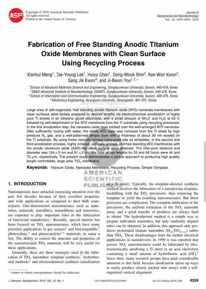
Fig 1 FESEM images of the as-prepared sample from (a) top view (b) bottom view (c) and (d) cross-sectional views In Figure 1(c) a TEM image
was inserted to show the tubular structure The sample was anodized for 24 h
Figure 1(a) shows the typical morphology of the top-
surface TiO2 membrane The image clearly reveals that the
entire surface of the ATO layer is covered with a layer
of nanowires which is attributed to the long time split of
the tube induced chemical etching in a ldquobamboo-splittingrdquo
mode2021 The nanowires were randomly arranged and
intersected As shown in Figure 1(b) the bottoms of the
TiO2 nanotubes were closed From the different magnified
cross-section views (Figs 1(c and d)) it can be seen that
the height of the first anodized ATO nanotubes membrane
with the nanowires is about 57 m and there is no tran-
sition area between the wire oxide layer and ordered bulk
ATO nanotubes The TEM image in Figure 1(c) shows the
tubular structure of the titanium oxide nanotubes fabricated
in first process
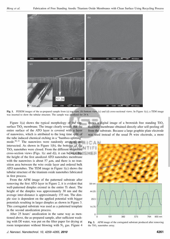
From the AFM image of the patterned substrate after
removing the first ATO layer in Figure 2 it is evident that
well-patterned dimples existed in the entire Ti sheet The
height of the dimples was approximately 30 nm and the
average inter-distance is approximately 155 nm The dim-
ple size is dependent on the applied potential with bigger
potentials resulting in larger dimples as shown in Figure 3
This corrugated substrate was used as a patterned template
in the second anodization process
After 25 hoursrsquo anodization in the same way as men-
tioned above the as-prepared sample after sufficient wash-
ing with DI water was put on the filter paper for drying at
room temperature without blowing with N2 gas Figure 4
shows a digital image of a brownish free standing TiO2
nanotube membrane obtained directly after self-peeling off
from the substrate Because a large graphite plate electrode
was used instead of the usual Pt wire electrode a more
0
59 nm
4425
295
1475
0191 382 573 764 955 nm
Fig 2 AFM image of the corrugated substrate produced after removing
the TiO2 nanotubes array
J Nanosci Nanotechnol 10 4259ndash4265 2010 4261
Delivered by Ingenta toSung Kyun Kwan University
IP 115145200148Thu 06 May 2010 120247
RESEARCH
ARTIC
LE
Fabrication of Free Standing Anodic Titanium Oxide Membranes with Clean Surface Using Recycling Process Meng et al
(a) (b)
(d)(c)
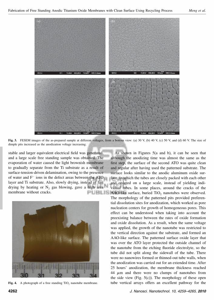
Fig 3 FESEM images of the as-prepared sample at different voltages from a bottom view (a) 30 V (b) 40 V (c) 50 V and (d) 60 V The size of
dimple pits increased as the anodization voltage increasing
stable and larger equivalent electrical field was generated
and a large scale free standing sample was obtained The
evaporation of water caused the light brownish membrane
to gradually separate from the Ti substrate as a result of
surface-tension-driven delamination owing to the presence
of water and Fminus ions in the defect areas between the ATO
layer and Ti substrate Also slowly drying instead of fast
drying by heating or N2 gas blowing gave a high area
membrane without cracks
Fig 4 A photograph of a free standing TiO2 nanotube membrane
As shown in Figures 5(a and b) it can be seen that
although the anodizing time was almost the same as the
first step the surface of the second ATO was quite clean
and regular after having used the patterned substrate The
surface looks similar to the anodic aluminum oxide sur-
face in which the tubes are closely packed with each other
and ordered on a large scale instead of yielding indi-
vidual tubes In some places around the cracks of the
AAO-like surface buried TiO2 nanotubes were observed
The morphology of the patterned pits provided preferen-
tial dissolution sites for anodization which worked as pore
nucleation centers for growth of homogeneous pores This
effect can be understood when taking into account the
preexisting balance between the rates of oxide formation
and oxide dissolution As a result when the same voltage
was applied the growth of the nanotube was restricted to
the vertical direction against the substrate and formed an
AAO-like surface The patterned surface oxide layer that
was over the ATO layer protected the outside channel of
the nanotube from the etching fluoride electrolyte so the
tube did not split along the sidewall of the tube There
were no nanowires formed or thinned-out tube walls when
the anodization was carried out for an extended time After
25 hoursrsquo anodization the membrane thickness reached
44 m and there were no clumps of nanotubes from
the side view (Fig 5(c)) The morphology of these open
tube vertical arrays offers an excellent pathway for the
4262 J Nanosci Nanotechnol 10 4259ndash4265 2010
Delivered by Ingenta toSung Kyun Kwan University
IP 115145200148Thu 06 May 2010 120247
RESEARCH
ARTIC
LE
Meng et al Fabrication of Free Standing Anodic Titanium Oxide Membranes with Clean Surface Using Recycling Process
(a)
(c)
(b)
(d)
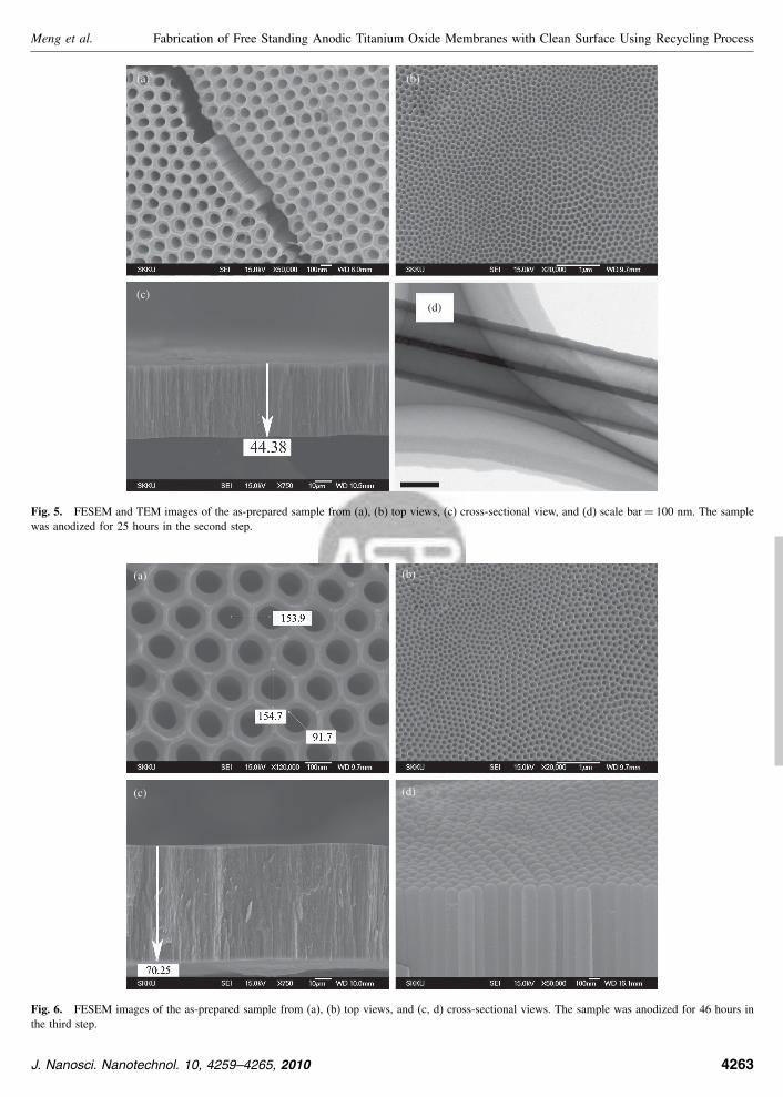
Fig 5 FESEM and TEM images of the as-prepared sample from (a) (b) top views (c) cross-sectional view and (d) scale bar= 100 nm The sample
was anodized for 25 hours in the second step
(a)
(c) (d)
(b)
Fig 6 FESEM images of the as-prepared sample from (a) (b) top views and (c d) cross-sectional views The sample was anodized for 46 hours in
the third step
J Nanosci Nanotechnol 10 4259ndash4265 2010 4263
Delivered by Ingenta toSung Kyun Kwan University
IP 115145200148Thu 06 May 2010 120247
RESEARCH
ARTIC
LE
Fabrication of Free Standing Anodic Titanium Oxide Membranes with Clean Surface Using Recycling Process Meng et al
(a) (b) (c)
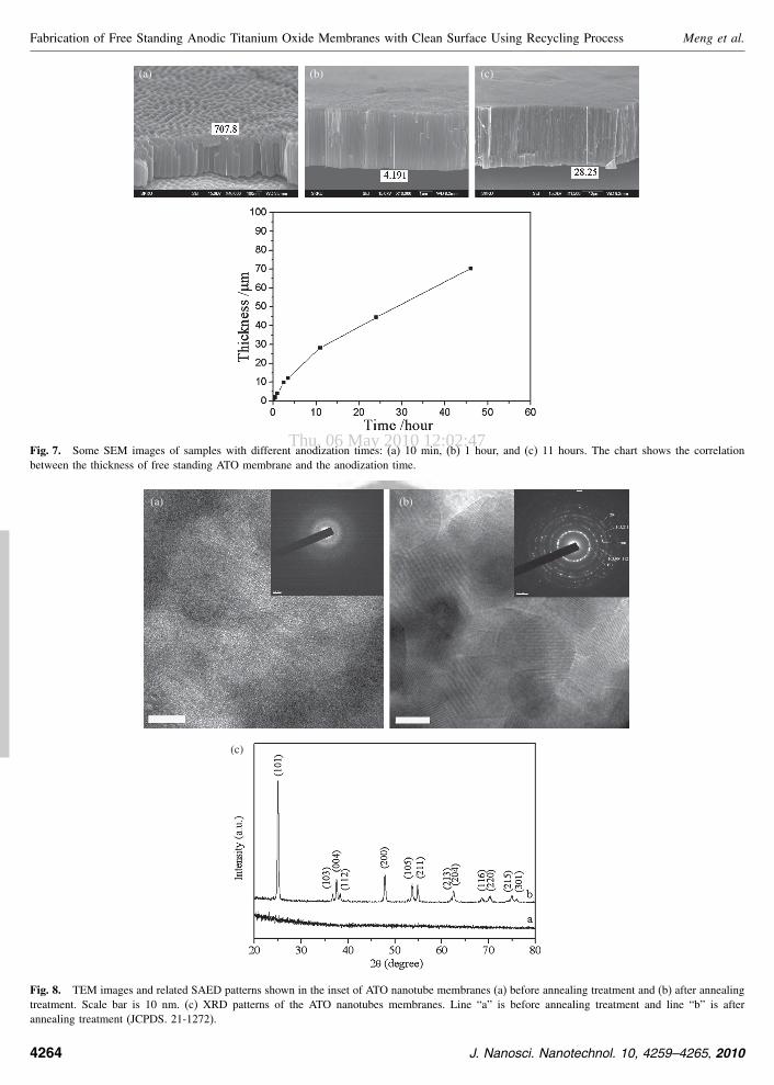
Fig 7 Some SEM images of samples with different anodization times (a) 10 min (b) 1 hour and (c) 11 hours The chart shows the correlation
between the thickness of free standing ATO membrane and the anodization time
(a) (b)
(c)
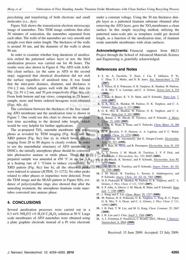
Fig 8 TEM images and related SAED patterns shown in the inset of ATO nanotube membranes (a) before annealing treatment and (b) after annealing
treatment Scale bar is 10 nm (c) XRD patterns of the ATO nanotubes membranes Line ldquoardquo is before annealing treatment and line ldquobrdquo is after
annealing treatment (JCPDS 21-1272)
4264 J Nanosci Nanotechnol 10 4259ndash4265 2010
Delivered by Ingenta toSung Kyun Kwan University
IP 115145200148Thu 06 May 2010 120247
RESEARCH
ARTIC
LE
Meng et al Fabrication of Free Standing Anodic Titanium Oxide Membranes with Clean Surface Using Recycling Process
percolating and transferring of both electrons and small
molecules (ie dye)
Figure 5(d) shows the transmission electron microscopy
image of nanotubes This TEM image confirms that after
30 minutes of sonication the nanotubes separated from
each other The walls of the nanotubes are very smooth and
straight over their entire length The thickness of the walls
is around 30 nm and the diameter of the walls is about
90 nm
In order to examine whether long durations of anodiza-
tion etched the patterned suface layer or not the third
anodization process was carried out for 46 hours The
results were also shown in Figure 6 The ATO with AAO-
like clean surface (as the same as ATO in the second
step) suggested that chemical dissolution did not etch
the surface regardless of anodized time It was found
that the inter-pore distance diameter and thickness is
154plusmn 2 nm (which agrees well with the AFM data (in
Fig 2)) 91plusmn2 nm and 70 m respectively (Figs 6(a c))
From both bottom and top views comparing to 25 hoursrsquo
sample more and better ordered hexagons were obtained
(Figs 6(b d))
The correlation between the thickness of the free stand-
ing ATO membrane and the anodization time is shown in
Figure 7 One could use this chart to choose the anodiza-
tion time according to the desired tube length which
would be very helpful for further applications
The as-prepared TiO2 nanotube membrane was amor-
phous as revealed by TEM imaging (Fig 8(a)) and the
XRD pattern (Fig 8(c) line a) in which broad spectra
ranging from 20 to 80 degree is clearly evident In order
to use the nanotubular structures of ATO membrane in
DSSCs the initially amorphous phase should be converted
into photoactive anatase or rutile phase Thus the as-
prepared sample was annealed at 450 C in air for 3 h
at a heating rate of 1 Cmin to induce crystallinity In
XRD pattern (Fig 8(c) line b) all the observed peaks
were indexed to anatase (JCPDS 21-1272) No other peaks
related to other phases or impurities were detected From
the TEM image and the SEAD pattern in Figure 8(b) evi-
dence of polycrystalline rings also showed that after the
annealing treatment the amorphous titanium oxide nano-
tubes converted into anatase phase
4 CONCLUSIONS
Several anodization processes were carried out in a
03 wt NH4F2 v H2O C2H6O2 solution at 50 V Large
scale membranes of ATO nanotubes were obtained using
a plate graphite electrode instead of a Pt wire electrode
under a constant voltage Using the 30 nm thickness dim-
ple layer as a patterned titanium substrate obtained after
removing the ATO layer gave the TiO2membranes a clean
surface In this simple recycling method utilizing the
patterned nano-scale pits as templates could get desired
length as a function of the anodization time of titanium
oxide nanotube membranes with clean surfaces
Acknowledgments Financial support from BK21
Project through the School of Advanced Materials Science
and Engineering is gratefully acknowledged
References and Notes
1 S Ju A Facchetti Y Xuan J Liu F Ishikawa P Ye
C Zhou T J Marks and D B Janes Nat Nanotechnol 2 378(2007)
2 S Yoriya H E Prakasam O K Varghese K Shankar M Paulose
G K Mor T A Latempa and C A Grimes Sensor Lett 4 334(2006)
3 J Park S Bauer K V D Mark and P Schmuki Nano Lett 71686 (2007)
4 G K Mor K Shankar M Paulose O K Varghese and C A
Grimes Nano Lett 6 215 (2006)5 G K Mor K Shankar M Paulose O K Varghese and C A
Grimes Nano Lett 5 191 (2005)6 E Balaur J M Macak H Tsuchiya and P Schmuki J Mater
Chem 15 4488 (2005)7 S Chu K Wada S Inoue and S Todoroki Chem Mater 14 266
(2002)8 D V Bavykin V N Parmon A A Lapkina and F C Walsh
J Mater Chem 14 3370 (2004)9 V Zwilling M Aucouturier and E Darque-Ceretti Electrochim
Acta 45 921 (1999)10 K S Raja M Misra and K Paramguru Electrochim Acta 51 154
(2005)11 L V Taveira J M Macak H Tsuchiya L F P Dick and
P Schmuki J Electrochem Soc 152 B405 (2005)12 J M Macak K Sirotna1 and P Schmuki Electrochim Acta 50
3679 (2005)13 J M Macak H Tsuchiya and P Schmuki Angew Chem Int Ed
44 2100 (2005)14 J M Macak H Tsuchiya L Taveira S Aldabergerova and
P Schmuki Angew Chem Int Ed 44 7463 (2005)15 H E Prakasam K Shankar M Paulose O K Varghese and C A
Grimes J Phys Chem C 111 7235 (2007)16 S P Albu A Ghicov J M Macak R Hahn and P Schmuki Nano
Lett 7 1286 (2007)17 J Wang and Z Lin Chem Mater 20 1257 (2008)18 M Paulose H E Prakasam O K Varghese L Peng K C Popat
G K Mor T A Desai and C A Grimes J Phys Chem C 111
14992 (2007)19 J H Park T W Lee and M G Kang Chem Commun 25 2867
(2008)20 J H Lim and J Choi Small 3 1504 (2007)21 A L Friedman E Panaitescu C Richter and L Menon J Nanosci
Nanotechnol 8 5864 (2008)
Received 15 June 2009 Accepted 23 July 2009
J Nanosci Nanotechnol 10 4259ndash4265 2010 4265

Delivered by Ingenta toSung Kyun Kwan University
IP 115145200148Thu 06 May 2010 120247
RESEARCH
ARTIC
LE
Fabrication of Free Standing Anodic Titanium Oxide Membranes with Clean Surface Using Recycling Process Meng et al
So far there have been three generations of anodic tita-
nium oxide (ATO) nanotubes In the first generation TiO2
nanotubes were fabricated in HF-based aqueous solutions
Some other inorganic acids and fluoride compounds such
as H3PO4NaF10 NH4F(NH42SO4
11 and Na2SO4NaF12
were used as a substitute for poisonous HF Due to the
rapid chemical dissolution rate the length of the obtained
nanotube was limited to 500 nm These low-aspect-ratio
tubes could not satisfy the requirements for applications
in dye sensitized solar cells (DSSCs) or filter membranes
Through adjusting the pH of the electrolyte the second
generation of ATO nanotubes was fabricated and tube
length was increased to a few micrometers13 In the third
generation by using an almost water-free polar solution
especially in viscous glycerol14 or ethylene glycol15 elec-
trolytes tens even hundreds of micron-length ATO nano-
tubes were easily prepared
However the above-mentioned TiO2 nanotubes were
attached to the Ti substrate which may limit their wider
application Recently many groups have attempted to
make self-organized free standing TiO2 nanotube arrays
Firstly Jan M Macak and co-workers directly fabricated
a flow-through TiO2 nanotubular membrane by selective
dissolution of Ti substrate and successfully used as a
photocatalytic microreactor16 This method was not only a
laborious process which took more than 10 hours but also
used a toxic bromine-containing methanol solution Then
Wang et al optimized the solution by using pure methanol
evaporation to delaminate the layer between the membrane
and the Ti foil17 Paulose et al described a process includ-
ing a critical point drying method by which nanotube array
films were able to be transformed into free-standing mem-
branes and applied it to control the diffusion of phenol
red18 More recently Park et al reported the preparation of
a membrane by immersing the Ti sheet with ATO in aque-
ous HCl solution for 1 h and made a glass-based DSSC19
However the above membrane surfaces were always cov-
ered by clumps of TiO2 nanotubes or nanowires To use the
free standing TiO2 nanotubes for a variety of applications
eg DSSCs this top layer should be removed to infiltrate
dye molecules and redox electrolytes into nanopores Post
treatments such as sonication or Al2O3 milling sometimes
needed several repetitions to ensure complete removal of
the top layer of nanowires These processes can cause
the membrane to crack So our aim is to end up with
as-received membranes with a clean surface at desired tube
lengths
Herein we report a simple and safe method to achieve
large scale self-organized freestanding and length con-
trollable ATO nanotube membranes by using the dimpled
substrate in the recycling process
2 EXPERIMENTAL DETAILS
Pure titanium foil (250 m in thickness and 997 purity)
was purchased from Sigma Aldrich and cut into the desired
size (40times50 cm) A direct current power supply (Agilent
E3612A) was used as the voltage source for the anodiza-
tion The anodization process was carried out in a two-
electrode configuration with titanium foil as the working
electrode and graphite (50times50 cm) as the counter elec-
trode under constant potential at 20 C The titanium sheets
were ultrasonicated in acetone isopropanol and methanol
each for 5 minutes followed by rinsing with de-ionized
(DI) water and drying in N2 gas The first electrochem-
ical treatment was carried out at 50 V in ethylene gly-
col with 03 wt NH4F and 2 v H2O for 24 hours
The as-prepared sample was rinsed immediately with DI
water for several minutes and dried with high pressure
N2 gas to remove the first ATO nanotube layer Using
the as-prepared patterned substrate without any treatment
the second anodic process was carried out at 50 V for
25 hours Then the sample was rinsed with DI water for
3 minutes and placed on a filter paper to evaporate the
water at room temperature The free standing ATO mem-
brane spontaneously separated from the substrate without
bending Using the same approach we anodized the sub-
strate obtained from the second anodization for 46 hours
in the third process
The morphology of the ATO was examined by JEOL
JSM-7000 field emission scanning electron microscopy
(FESEM) The cross-section photographs were obtained
by observing a mechanically fractured ATO layer trans-
ferred onto an adhesive carbon tape coated with 3 nm
Pt The specimen for transmission electron microscopy
(TEM JEOL-2100F) at 200 kV was prepared by soni-
cating a small part of the ATO membrane in ethanol for
30 minutes and observing on a carbon-coated copper grid
The dimple substrate after first anodization was charac-
terized by Atomic Force Microscopy (AFM) In order to
examine the phase transition the as-prepared sample was
annealed at 450 C in air for 3 hours at a heating rate
of 1 Cmin TEM images were also obtained using the
above-mentioned method X-ray diffraction (XRD) was
performed (Rigaku Rotafles) using CuK (015416 nm)
radiation
3 RESULTS AND DISCUSSION
After anodization for 24 hours the ATO layer with the
Ti substrate was washed with DI water for 3 min A sud-
den color change was observed which indicated that water
had completely penetrated into the pores and reached the
substrate When this happened the ATO layer was eas-
ily removed by subsequent blowing with high pressure N2
gas and broken into several pieces The easy detachment
of the ATO layer discovered here is a notable feature
particularly given that long-time immersion of the ATO
layer in methanol or HCl solution was not required The
ATO membrane and the Ti substrate were characterized as
follows
4260 J Nanosci Nanotechnol 10 4259ndash4265 2010
Delivered by Ingenta toSung Kyun Kwan University
IP 115145200148Thu 06 May 2010 120247
RESEARCH
ARTIC
LE
Meng et al Fabrication of Free Standing Anodic Titanium Oxide Membranes with Clean Surface Using Recycling Process
(a)
(c) (d)
(b)
Fig 1 FESEM images of the as-prepared sample from (a) top view (b) bottom view (c) and (d) cross-sectional views In Figure 1(c) a TEM image
was inserted to show the tubular structure The sample was anodized for 24 h
Figure 1(a) shows the typical morphology of the top-
surface TiO2 membrane The image clearly reveals that the
entire surface of the ATO layer is covered with a layer
of nanowires which is attributed to the long time split of
the tube induced chemical etching in a ldquobamboo-splittingrdquo
mode2021 The nanowires were randomly arranged and
intersected As shown in Figure 1(b) the bottoms of the
TiO2 nanotubes were closed From the different magnified
cross-section views (Figs 1(c and d)) it can be seen that
the height of the first anodized ATO nanotubes membrane
with the nanowires is about 57 m and there is no tran-
sition area between the wire oxide layer and ordered bulk
ATO nanotubes The TEM image in Figure 1(c) shows the
tubular structure of the titanium oxide nanotubes fabricated
in first process
From the AFM image of the patterned substrate after
removing the first ATO layer in Figure 2 it is evident that
well-patterned dimples existed in the entire Ti sheet The
height of the dimples was approximately 30 nm and the
average inter-distance is approximately 155 nm The dim-
ple size is dependent on the applied potential with bigger
potentials resulting in larger dimples as shown in Figure 3
This corrugated substrate was used as a patterned template
in the second anodization process
After 25 hoursrsquo anodization in the same way as men-
tioned above the as-prepared sample after sufficient wash-
ing with DI water was put on the filter paper for drying at
room temperature without blowing with N2 gas Figure 4
shows a digital image of a brownish free standing TiO2
nanotube membrane obtained directly after self-peeling off
from the substrate Because a large graphite plate electrode
was used instead of the usual Pt wire electrode a more
0
59 nm
4425
295
1475
0191 382 573 764 955 nm
Fig 2 AFM image of the corrugated substrate produced after removing
the TiO2 nanotubes array
J Nanosci Nanotechnol 10 4259ndash4265 2010 4261
Delivered by Ingenta toSung Kyun Kwan University
IP 115145200148Thu 06 May 2010 120247
RESEARCH
ARTIC
LE
Fabrication of Free Standing Anodic Titanium Oxide Membranes with Clean Surface Using Recycling Process Meng et al
(a) (b)
(d)(c)
Fig 3 FESEM images of the as-prepared sample at different voltages from a bottom view (a) 30 V (b) 40 V (c) 50 V and (d) 60 V The size of
dimple pits increased as the anodization voltage increasing
stable and larger equivalent electrical field was generated
and a large scale free standing sample was obtained The
evaporation of water caused the light brownish membrane
to gradually separate from the Ti substrate as a result of
surface-tension-driven delamination owing to the presence
of water and Fminus ions in the defect areas between the ATO
layer and Ti substrate Also slowly drying instead of fast
drying by heating or N2 gas blowing gave a high area
membrane without cracks
Fig 4 A photograph of a free standing TiO2 nanotube membrane
As shown in Figures 5(a and b) it can be seen that
although the anodizing time was almost the same as the
first step the surface of the second ATO was quite clean
and regular after having used the patterned substrate The
surface looks similar to the anodic aluminum oxide sur-
face in which the tubes are closely packed with each other
and ordered on a large scale instead of yielding indi-
vidual tubes In some places around the cracks of the
AAO-like surface buried TiO2 nanotubes were observed
The morphology of the patterned pits provided preferen-
tial dissolution sites for anodization which worked as pore
nucleation centers for growth of homogeneous pores This
effect can be understood when taking into account the
preexisting balance between the rates of oxide formation
and oxide dissolution As a result when the same voltage
was applied the growth of the nanotube was restricted to
the vertical direction against the substrate and formed an
AAO-like surface The patterned surface oxide layer that
was over the ATO layer protected the outside channel of
the nanotube from the etching fluoride electrolyte so the
tube did not split along the sidewall of the tube There
were no nanowires formed or thinned-out tube walls when
the anodization was carried out for an extended time After
25 hoursrsquo anodization the membrane thickness reached
44 m and there were no clumps of nanotubes from
the side view (Fig 5(c)) The morphology of these open
tube vertical arrays offers an excellent pathway for the
4262 J Nanosci Nanotechnol 10 4259ndash4265 2010
Delivered by Ingenta toSung Kyun Kwan University
IP 115145200148Thu 06 May 2010 120247
RESEARCH
ARTIC
LE
Meng et al Fabrication of Free Standing Anodic Titanium Oxide Membranes with Clean Surface Using Recycling Process
(a)
(c)
(b)
(d)
Fig 5 FESEM and TEM images of the as-prepared sample from (a) (b) top views (c) cross-sectional view and (d) scale bar= 100 nm The sample
was anodized for 25 hours in the second step
(a)
(c) (d)
(b)
Fig 6 FESEM images of the as-prepared sample from (a) (b) top views and (c d) cross-sectional views The sample was anodized for 46 hours in
the third step
J Nanosci Nanotechnol 10 4259ndash4265 2010 4263
Delivered by Ingenta toSung Kyun Kwan University
IP 115145200148Thu 06 May 2010 120247
RESEARCH
ARTIC
LE
Fabrication of Free Standing Anodic Titanium Oxide Membranes with Clean Surface Using Recycling Process Meng et al
(a) (b) (c)
Fig 7 Some SEM images of samples with different anodization times (a) 10 min (b) 1 hour and (c) 11 hours The chart shows the correlation
between the thickness of free standing ATO membrane and the anodization time
(a) (b)
(c)
Fig 8 TEM images and related SAED patterns shown in the inset of ATO nanotube membranes (a) before annealing treatment and (b) after annealing
treatment Scale bar is 10 nm (c) XRD patterns of the ATO nanotubes membranes Line ldquoardquo is before annealing treatment and line ldquobrdquo is after
annealing treatment (JCPDS 21-1272)
4264 J Nanosci Nanotechnol 10 4259ndash4265 2010
Delivered by Ingenta toSung Kyun Kwan University
IP 115145200148Thu 06 May 2010 120247
RESEARCH
ARTIC
LE
Meng et al Fabrication of Free Standing Anodic Titanium Oxide Membranes with Clean Surface Using Recycling Process
percolating and transferring of both electrons and small
molecules (ie dye)
Figure 5(d) shows the transmission electron microscopy
image of nanotubes This TEM image confirms that after
30 minutes of sonication the nanotubes separated from
each other The walls of the nanotubes are very smooth and
straight over their entire length The thickness of the walls
is around 30 nm and the diameter of the walls is about
90 nm
In order to examine whether long durations of anodiza-
tion etched the patterned suface layer or not the third
anodization process was carried out for 46 hours The
results were also shown in Figure 6 The ATO with AAO-
like clean surface (as the same as ATO in the second
step) suggested that chemical dissolution did not etch
the surface regardless of anodized time It was found
that the inter-pore distance diameter and thickness is
154plusmn 2 nm (which agrees well with the AFM data (in
Fig 2)) 91plusmn2 nm and 70 m respectively (Figs 6(a c))
From both bottom and top views comparing to 25 hoursrsquo
sample more and better ordered hexagons were obtained
(Figs 6(b d))
The correlation between the thickness of the free stand-
ing ATO membrane and the anodization time is shown in
Figure 7 One could use this chart to choose the anodiza-
tion time according to the desired tube length which
would be very helpful for further applications
The as-prepared TiO2 nanotube membrane was amor-
phous as revealed by TEM imaging (Fig 8(a)) and the
XRD pattern (Fig 8(c) line a) in which broad spectra
ranging from 20 to 80 degree is clearly evident In order
to use the nanotubular structures of ATO membrane in
DSSCs the initially amorphous phase should be converted
into photoactive anatase or rutile phase Thus the as-
prepared sample was annealed at 450 C in air for 3 h
at a heating rate of 1 Cmin to induce crystallinity In
XRD pattern (Fig 8(c) line b) all the observed peaks
were indexed to anatase (JCPDS 21-1272) No other peaks
related to other phases or impurities were detected From
the TEM image and the SEAD pattern in Figure 8(b) evi-
dence of polycrystalline rings also showed that after the
annealing treatment the amorphous titanium oxide nano-
tubes converted into anatase phase
4 CONCLUSIONS
Several anodization processes were carried out in a
03 wt NH4F2 v H2O C2H6O2 solution at 50 V Large
scale membranes of ATO nanotubes were obtained using
a plate graphite electrode instead of a Pt wire electrode
under a constant voltage Using the 30 nm thickness dim-
ple layer as a patterned titanium substrate obtained after
removing the ATO layer gave the TiO2membranes a clean
surface In this simple recycling method utilizing the
patterned nano-scale pits as templates could get desired
length as a function of the anodization time of titanium
oxide nanotube membranes with clean surfaces
Acknowledgments Financial support from BK21
Project through the School of Advanced Materials Science
and Engineering is gratefully acknowledged
References and Notes
1 S Ju A Facchetti Y Xuan J Liu F Ishikawa P Ye
C Zhou T J Marks and D B Janes Nat Nanotechnol 2 378(2007)
2 S Yoriya H E Prakasam O K Varghese K Shankar M Paulose
G K Mor T A Latempa and C A Grimes Sensor Lett 4 334(2006)
3 J Park S Bauer K V D Mark and P Schmuki Nano Lett 71686 (2007)
4 G K Mor K Shankar M Paulose O K Varghese and C A
Grimes Nano Lett 6 215 (2006)5 G K Mor K Shankar M Paulose O K Varghese and C A
Grimes Nano Lett 5 191 (2005)6 E Balaur J M Macak H Tsuchiya and P Schmuki J Mater
Chem 15 4488 (2005)7 S Chu K Wada S Inoue and S Todoroki Chem Mater 14 266
(2002)8 D V Bavykin V N Parmon A A Lapkina and F C Walsh
J Mater Chem 14 3370 (2004)9 V Zwilling M Aucouturier and E Darque-Ceretti Electrochim
Acta 45 921 (1999)10 K S Raja M Misra and K Paramguru Electrochim Acta 51 154
(2005)11 L V Taveira J M Macak H Tsuchiya L F P Dick and
P Schmuki J Electrochem Soc 152 B405 (2005)12 J M Macak K Sirotna1 and P Schmuki Electrochim Acta 50
3679 (2005)13 J M Macak H Tsuchiya and P Schmuki Angew Chem Int Ed
44 2100 (2005)14 J M Macak H Tsuchiya L Taveira S Aldabergerova and
P Schmuki Angew Chem Int Ed 44 7463 (2005)15 H E Prakasam K Shankar M Paulose O K Varghese and C A
Grimes J Phys Chem C 111 7235 (2007)16 S P Albu A Ghicov J M Macak R Hahn and P Schmuki Nano
Lett 7 1286 (2007)17 J Wang and Z Lin Chem Mater 20 1257 (2008)18 M Paulose H E Prakasam O K Varghese L Peng K C Popat
G K Mor T A Desai and C A Grimes J Phys Chem C 111
14992 (2007)19 J H Park T W Lee and M G Kang Chem Commun 25 2867
(2008)20 J H Lim and J Choi Small 3 1504 (2007)21 A L Friedman E Panaitescu C Richter and L Menon J Nanosci
Nanotechnol 8 5864 (2008)
Received 15 June 2009 Accepted 23 July 2009
J Nanosci Nanotechnol 10 4259ndash4265 2010 4265
Delivered by Ingenta toSung Kyun Kwan University
IP 115145200148Thu 06 May 2010 120247
RESEARCH
ARTIC
LE
Meng et al Fabrication of Free Standing Anodic Titanium Oxide Membranes with Clean Surface Using Recycling Process
(a)
(c) (d)
(b)
Fig 1 FESEM images of the as-prepared sample from (a) top view (b) bottom view (c) and (d) cross-sectional views In Figure 1(c) a TEM image
was inserted to show the tubular structure The sample was anodized for 24 h
Figure 1(a) shows the typical morphology of the top-
surface TiO2 membrane The image clearly reveals that the
entire surface of the ATO layer is covered with a layer
of nanowires which is attributed to the long time split of
the tube induced chemical etching in a ldquobamboo-splittingrdquo
mode2021 The nanowires were randomly arranged and
intersected As shown in Figure 1(b) the bottoms of the
TiO2 nanotubes were closed From the different magnified
cross-section views (Figs 1(c and d)) it can be seen that
the height of the first anodized ATO nanotubes membrane
with the nanowires is about 57 m and there is no tran-
sition area between the wire oxide layer and ordered bulk
ATO nanotubes The TEM image in Figure 1(c) shows the
tubular structure of the titanium oxide nanotubes fabricated
in first process
From the AFM image of the patterned substrate after
removing the first ATO layer in Figure 2 it is evident that
well-patterned dimples existed in the entire Ti sheet The
height of the dimples was approximately 30 nm and the
average inter-distance is approximately 155 nm The dim-
ple size is dependent on the applied potential with bigger
potentials resulting in larger dimples as shown in Figure 3
This corrugated substrate was used as a patterned template
in the second anodization process
After 25 hoursrsquo anodization in the same way as men-
tioned above the as-prepared sample after sufficient wash-
ing with DI water was put on the filter paper for drying at
room temperature without blowing with N2 gas Figure 4
shows a digital image of a brownish free standing TiO2
nanotube membrane obtained directly after self-peeling off
from the substrate Because a large graphite plate electrode
was used instead of the usual Pt wire electrode a more
0
59 nm
4425
295
1475
0191 382 573 764 955 nm
Fig 2 AFM image of the corrugated substrate produced after removing
the TiO2 nanotubes array
J Nanosci Nanotechnol 10 4259ndash4265 2010 4261
Delivered by Ingenta toSung Kyun Kwan University
IP 115145200148Thu 06 May 2010 120247
RESEARCH
ARTIC
LE
Fabrication of Free Standing Anodic Titanium Oxide Membranes with Clean Surface Using Recycling Process Meng et al
(a) (b)
(d)(c)
Fig 3 FESEM images of the as-prepared sample at different voltages from a bottom view (a) 30 V (b) 40 V (c) 50 V and (d) 60 V The size of
dimple pits increased as the anodization voltage increasing
stable and larger equivalent electrical field was generated
and a large scale free standing sample was obtained The
evaporation of water caused the light brownish membrane
to gradually separate from the Ti substrate as a result of
surface-tension-driven delamination owing to the presence
of water and Fminus ions in the defect areas between the ATO
layer and Ti substrate Also slowly drying instead of fast
drying by heating or N2 gas blowing gave a high area
membrane without cracks
Fig 4 A photograph of a free standing TiO2 nanotube membrane
As shown in Figures 5(a and b) it can be seen that
although the anodizing time was almost the same as the
first step the surface of the second ATO was quite clean
and regular after having used the patterned substrate The
surface looks similar to the anodic aluminum oxide sur-
face in which the tubes are closely packed with each other
and ordered on a large scale instead of yielding indi-
vidual tubes In some places around the cracks of the
AAO-like surface buried TiO2 nanotubes were observed
The morphology of the patterned pits provided preferen-
tial dissolution sites for anodization which worked as pore
nucleation centers for growth of homogeneous pores This
effect can be understood when taking into account the
preexisting balance between the rates of oxide formation
and oxide dissolution As a result when the same voltage
was applied the growth of the nanotube was restricted to
the vertical direction against the substrate and formed an
AAO-like surface The patterned surface oxide layer that
was over the ATO layer protected the outside channel of
the nanotube from the etching fluoride electrolyte so the
tube did not split along the sidewall of the tube There
were no nanowires formed or thinned-out tube walls when
the anodization was carried out for an extended time After
25 hoursrsquo anodization the membrane thickness reached
44 m and there were no clumps of nanotubes from
the side view (Fig 5(c)) The morphology of these open
tube vertical arrays offers an excellent pathway for the
4262 J Nanosci Nanotechnol 10 4259ndash4265 2010
Delivered by Ingenta toSung Kyun Kwan University
IP 115145200148Thu 06 May 2010 120247
RESEARCH
ARTIC
LE
Meng et al Fabrication of Free Standing Anodic Titanium Oxide Membranes with Clean Surface Using Recycling Process
(a)
(c)
(b)
(d)
Fig 5 FESEM and TEM images of the as-prepared sample from (a) (b) top views (c) cross-sectional view and (d) scale bar= 100 nm The sample
was anodized for 25 hours in the second step
(a)
(c) (d)
(b)
Fig 6 FESEM images of the as-prepared sample from (a) (b) top views and (c d) cross-sectional views The sample was anodized for 46 hours in
the third step
J Nanosci Nanotechnol 10 4259ndash4265 2010 4263
Delivered by Ingenta toSung Kyun Kwan University
IP 115145200148Thu 06 May 2010 120247
RESEARCH
ARTIC
LE
Fabrication of Free Standing Anodic Titanium Oxide Membranes with Clean Surface Using Recycling Process Meng et al
(a) (b) (c)
Fig 7 Some SEM images of samples with different anodization times (a) 10 min (b) 1 hour and (c) 11 hours The chart shows the correlation
between the thickness of free standing ATO membrane and the anodization time
(a) (b)
(c)
Fig 8 TEM images and related SAED patterns shown in the inset of ATO nanotube membranes (a) before annealing treatment and (b) after annealing
treatment Scale bar is 10 nm (c) XRD patterns of the ATO nanotubes membranes Line ldquoardquo is before annealing treatment and line ldquobrdquo is after
annealing treatment (JCPDS 21-1272)
4264 J Nanosci Nanotechnol 10 4259ndash4265 2010
Delivered by Ingenta toSung Kyun Kwan University
IP 115145200148Thu 06 May 2010 120247
RESEARCH
ARTIC
LE
Meng et al Fabrication of Free Standing Anodic Titanium Oxide Membranes with Clean Surface Using Recycling Process
percolating and transferring of both electrons and small
molecules (ie dye)
Figure 5(d) shows the transmission electron microscopy
image of nanotubes This TEM image confirms that after
30 minutes of sonication the nanotubes separated from
each other The walls of the nanotubes are very smooth and
straight over their entire length The thickness of the walls
is around 30 nm and the diameter of the walls is about
90 nm
In order to examine whether long durations of anodiza-
tion etched the patterned suface layer or not the third
anodization process was carried out for 46 hours The
results were also shown in Figure 6 The ATO with AAO-
like clean surface (as the same as ATO in the second
step) suggested that chemical dissolution did not etch
the surface regardless of anodized time It was found
that the inter-pore distance diameter and thickness is
154plusmn 2 nm (which agrees well with the AFM data (in
Fig 2)) 91plusmn2 nm and 70 m respectively (Figs 6(a c))
From both bottom and top views comparing to 25 hoursrsquo
sample more and better ordered hexagons were obtained
(Figs 6(b d))
The correlation between the thickness of the free stand-
ing ATO membrane and the anodization time is shown in
Figure 7 One could use this chart to choose the anodiza-
tion time according to the desired tube length which
would be very helpful for further applications
The as-prepared TiO2 nanotube membrane was amor-
phous as revealed by TEM imaging (Fig 8(a)) and the
XRD pattern (Fig 8(c) line a) in which broad spectra
ranging from 20 to 80 degree is clearly evident In order
to use the nanotubular structures of ATO membrane in
DSSCs the initially amorphous phase should be converted
into photoactive anatase or rutile phase Thus the as-
prepared sample was annealed at 450 C in air for 3 h
at a heating rate of 1 Cmin to induce crystallinity In
XRD pattern (Fig 8(c) line b) all the observed peaks
were indexed to anatase (JCPDS 21-1272) No other peaks
related to other phases or impurities were detected From
the TEM image and the SEAD pattern in Figure 8(b) evi-
dence of polycrystalline rings also showed that after the
annealing treatment the amorphous titanium oxide nano-
tubes converted into anatase phase
4 CONCLUSIONS
Several anodization processes were carried out in a
03 wt NH4F2 v H2O C2H6O2 solution at 50 V Large
scale membranes of ATO nanotubes were obtained using
a plate graphite electrode instead of a Pt wire electrode
under a constant voltage Using the 30 nm thickness dim-
ple layer as a patterned titanium substrate obtained after
removing the ATO layer gave the TiO2membranes a clean
surface In this simple recycling method utilizing the
patterned nano-scale pits as templates could get desired
length as a function of the anodization time of titanium
oxide nanotube membranes with clean surfaces
Acknowledgments Financial support from BK21
Project through the School of Advanced Materials Science
and Engineering is gratefully acknowledged
References and Notes
1 S Ju A Facchetti Y Xuan J Liu F Ishikawa P Ye
C Zhou T J Marks and D B Janes Nat Nanotechnol 2 378(2007)
2 S Yoriya H E Prakasam O K Varghese K Shankar M Paulose
G K Mor T A Latempa and C A Grimes Sensor Lett 4 334(2006)
3 J Park S Bauer K V D Mark and P Schmuki Nano Lett 71686 (2007)
4 G K Mor K Shankar M Paulose O K Varghese and C A
Grimes Nano Lett 6 215 (2006)5 G K Mor K Shankar M Paulose O K Varghese and C A
Grimes Nano Lett 5 191 (2005)6 E Balaur J M Macak H Tsuchiya and P Schmuki J Mater
Chem 15 4488 (2005)7 S Chu K Wada S Inoue and S Todoroki Chem Mater 14 266
(2002)8 D V Bavykin V N Parmon A A Lapkina and F C Walsh
J Mater Chem 14 3370 (2004)9 V Zwilling M Aucouturier and E Darque-Ceretti Electrochim
Acta 45 921 (1999)10 K S Raja M Misra and K Paramguru Electrochim Acta 51 154
(2005)11 L V Taveira J M Macak H Tsuchiya L F P Dick and
P Schmuki J Electrochem Soc 152 B405 (2005)12 J M Macak K Sirotna1 and P Schmuki Electrochim Acta 50
3679 (2005)13 J M Macak H Tsuchiya and P Schmuki Angew Chem Int Ed
44 2100 (2005)14 J M Macak H Tsuchiya L Taveira S Aldabergerova and
P Schmuki Angew Chem Int Ed 44 7463 (2005)15 H E Prakasam K Shankar M Paulose O K Varghese and C A
Grimes J Phys Chem C 111 7235 (2007)16 S P Albu A Ghicov J M Macak R Hahn and P Schmuki Nano
Lett 7 1286 (2007)17 J Wang and Z Lin Chem Mater 20 1257 (2008)18 M Paulose H E Prakasam O K Varghese L Peng K C Popat
G K Mor T A Desai and C A Grimes J Phys Chem C 111
14992 (2007)19 J H Park T W Lee and M G Kang Chem Commun 25 2867
(2008)20 J H Lim and J Choi Small 3 1504 (2007)21 A L Friedman E Panaitescu C Richter and L Menon J Nanosci
Nanotechnol 8 5864 (2008)
Received 15 June 2009 Accepted 23 July 2009
J Nanosci Nanotechnol 10 4259ndash4265 2010 4265
Delivered by Ingenta toSung Kyun Kwan University
IP 115145200148Thu 06 May 2010 120247
RESEARCH
ARTIC
LE
Fabrication of Free Standing Anodic Titanium Oxide Membranes with Clean Surface Using Recycling Process Meng et al
(a) (b)
(d)(c)
Fig 3 FESEM images of the as-prepared sample at different voltages from a bottom view (a) 30 V (b) 40 V (c) 50 V and (d) 60 V The size of
dimple pits increased as the anodization voltage increasing
stable and larger equivalent electrical field was generated
and a large scale free standing sample was obtained The
evaporation of water caused the light brownish membrane
to gradually separate from the Ti substrate as a result of
surface-tension-driven delamination owing to the presence
of water and Fminus ions in the defect areas between the ATO
layer and Ti substrate Also slowly drying instead of fast
drying by heating or N2 gas blowing gave a high area
membrane without cracks
Fig 4 A photograph of a free standing TiO2 nanotube membrane
As shown in Figures 5(a and b) it can be seen that
although the anodizing time was almost the same as the
first step the surface of the second ATO was quite clean
and regular after having used the patterned substrate The
surface looks similar to the anodic aluminum oxide sur-
face in which the tubes are closely packed with each other
and ordered on a large scale instead of yielding indi-
vidual tubes In some places around the cracks of the
AAO-like surface buried TiO2 nanotubes were observed
The morphology of the patterned pits provided preferen-
tial dissolution sites for anodization which worked as pore
nucleation centers for growth of homogeneous pores This
effect can be understood when taking into account the
preexisting balance between the rates of oxide formation
and oxide dissolution As a result when the same voltage
was applied the growth of the nanotube was restricted to
the vertical direction against the substrate and formed an
AAO-like surface The patterned surface oxide layer that
was over the ATO layer protected the outside channel of
the nanotube from the etching fluoride electrolyte so the
tube did not split along the sidewall of the tube There
were no nanowires formed or thinned-out tube walls when
the anodization was carried out for an extended time After
25 hoursrsquo anodization the membrane thickness reached
44 m and there were no clumps of nanotubes from
the side view (Fig 5(c)) The morphology of these open
tube vertical arrays offers an excellent pathway for the
4262 J Nanosci Nanotechnol 10 4259ndash4265 2010
Delivered by Ingenta toSung Kyun Kwan University
IP 115145200148Thu 06 May 2010 120247
RESEARCH
ARTIC
LE
Meng et al Fabrication of Free Standing Anodic Titanium Oxide Membranes with Clean Surface Using Recycling Process
(a)
(c)
(b)
(d)
Fig 5 FESEM and TEM images of the as-prepared sample from (a) (b) top views (c) cross-sectional view and (d) scale bar= 100 nm The sample
was anodized for 25 hours in the second step
(a)
(c) (d)
(b)
Fig 6 FESEM images of the as-prepared sample from (a) (b) top views and (c d) cross-sectional views The sample was anodized for 46 hours in
the third step
J Nanosci Nanotechnol 10 4259ndash4265 2010 4263
Delivered by Ingenta toSung Kyun Kwan University
IP 115145200148Thu 06 May 2010 120247
RESEARCH
ARTIC
LE
Fabrication of Free Standing Anodic Titanium Oxide Membranes with Clean Surface Using Recycling Process Meng et al
(a) (b) (c)
Fig 7 Some SEM images of samples with different anodization times (a) 10 min (b) 1 hour and (c) 11 hours The chart shows the correlation
between the thickness of free standing ATO membrane and the anodization time
(a) (b)
(c)
Fig 8 TEM images and related SAED patterns shown in the inset of ATO nanotube membranes (a) before annealing treatment and (b) after annealing
treatment Scale bar is 10 nm (c) XRD patterns of the ATO nanotubes membranes Line ldquoardquo is before annealing treatment and line ldquobrdquo is after
annealing treatment (JCPDS 21-1272)
4264 J Nanosci Nanotechnol 10 4259ndash4265 2010
Delivered by Ingenta toSung Kyun Kwan University
IP 115145200148Thu 06 May 2010 120247
RESEARCH
ARTIC
LE
Meng et al Fabrication of Free Standing Anodic Titanium Oxide Membranes with Clean Surface Using Recycling Process
percolating and transferring of both electrons and small
molecules (ie dye)
Figure 5(d) shows the transmission electron microscopy
image of nanotubes This TEM image confirms that after
30 minutes of sonication the nanotubes separated from
each other The walls of the nanotubes are very smooth and
straight over their entire length The thickness of the walls
is around 30 nm and the diameter of the walls is about
90 nm
In order to examine whether long durations of anodiza-
tion etched the patterned suface layer or not the third
anodization process was carried out for 46 hours The
results were also shown in Figure 6 The ATO with AAO-
like clean surface (as the same as ATO in the second
step) suggested that chemical dissolution did not etch
the surface regardless of anodized time It was found
that the inter-pore distance diameter and thickness is
154plusmn 2 nm (which agrees well with the AFM data (in
Fig 2)) 91plusmn2 nm and 70 m respectively (Figs 6(a c))
From both bottom and top views comparing to 25 hoursrsquo
sample more and better ordered hexagons were obtained
(Figs 6(b d))
The correlation between the thickness of the free stand-
ing ATO membrane and the anodization time is shown in
Figure 7 One could use this chart to choose the anodiza-
tion time according to the desired tube length which
would be very helpful for further applications
The as-prepared TiO2 nanotube membrane was amor-
phous as revealed by TEM imaging (Fig 8(a)) and the
XRD pattern (Fig 8(c) line a) in which broad spectra
ranging from 20 to 80 degree is clearly evident In order
to use the nanotubular structures of ATO membrane in
DSSCs the initially amorphous phase should be converted
into photoactive anatase or rutile phase Thus the as-
prepared sample was annealed at 450 C in air for 3 h
at a heating rate of 1 Cmin to induce crystallinity In
XRD pattern (Fig 8(c) line b) all the observed peaks
were indexed to anatase (JCPDS 21-1272) No other peaks
related to other phases or impurities were detected From
the TEM image and the SEAD pattern in Figure 8(b) evi-
dence of polycrystalline rings also showed that after the
annealing treatment the amorphous titanium oxide nano-
tubes converted into anatase phase
4 CONCLUSIONS
Several anodization processes were carried out in a
03 wt NH4F2 v H2O C2H6O2 solution at 50 V Large
scale membranes of ATO nanotubes were obtained using
a plate graphite electrode instead of a Pt wire electrode
under a constant voltage Using the 30 nm thickness dim-
ple layer as a patterned titanium substrate obtained after
removing the ATO layer gave the TiO2membranes a clean
surface In this simple recycling method utilizing the
patterned nano-scale pits as templates could get desired
length as a function of the anodization time of titanium
oxide nanotube membranes with clean surfaces
Acknowledgments Financial support from BK21
Project through the School of Advanced Materials Science
and Engineering is gratefully acknowledged
References and Notes
1 S Ju A Facchetti Y Xuan J Liu F Ishikawa P Ye
C Zhou T J Marks and D B Janes Nat Nanotechnol 2 378(2007)
2 S Yoriya H E Prakasam O K Varghese K Shankar M Paulose
G K Mor T A Latempa and C A Grimes Sensor Lett 4 334(2006)
3 J Park S Bauer K V D Mark and P Schmuki Nano Lett 71686 (2007)
4 G K Mor K Shankar M Paulose O K Varghese and C A
Grimes Nano Lett 6 215 (2006)5 G K Mor K Shankar M Paulose O K Varghese and C A
Grimes Nano Lett 5 191 (2005)6 E Balaur J M Macak H Tsuchiya and P Schmuki J Mater
Chem 15 4488 (2005)7 S Chu K Wada S Inoue and S Todoroki Chem Mater 14 266
(2002)8 D V Bavykin V N Parmon A A Lapkina and F C Walsh
J Mater Chem 14 3370 (2004)9 V Zwilling M Aucouturier and E Darque-Ceretti Electrochim
Acta 45 921 (1999)10 K S Raja M Misra and K Paramguru Electrochim Acta 51 154
(2005)11 L V Taveira J M Macak H Tsuchiya L F P Dick and
P Schmuki J Electrochem Soc 152 B405 (2005)12 J M Macak K Sirotna1 and P Schmuki Electrochim Acta 50
3679 (2005)13 J M Macak H Tsuchiya and P Schmuki Angew Chem Int Ed
44 2100 (2005)14 J M Macak H Tsuchiya L Taveira S Aldabergerova and
P Schmuki Angew Chem Int Ed 44 7463 (2005)15 H E Prakasam K Shankar M Paulose O K Varghese and C A
Grimes J Phys Chem C 111 7235 (2007)16 S P Albu A Ghicov J M Macak R Hahn and P Schmuki Nano
Lett 7 1286 (2007)17 J Wang and Z Lin Chem Mater 20 1257 (2008)18 M Paulose H E Prakasam O K Varghese L Peng K C Popat
G K Mor T A Desai and C A Grimes J Phys Chem C 111
14992 (2007)19 J H Park T W Lee and M G Kang Chem Commun 25 2867
(2008)20 J H Lim and J Choi Small 3 1504 (2007)21 A L Friedman E Panaitescu C Richter and L Menon J Nanosci
Nanotechnol 8 5864 (2008)
Received 15 June 2009 Accepted 23 July 2009
J Nanosci Nanotechnol 10 4259ndash4265 2010 4265
Delivered by Ingenta toSung Kyun Kwan University
IP 115145200148Thu 06 May 2010 120247
RESEARCH
ARTIC
LE
Meng et al Fabrication of Free Standing Anodic Titanium Oxide Membranes with Clean Surface Using Recycling Process
(a)
(c)
(b)
(d)
Fig 5 FESEM and TEM images of the as-prepared sample from (a) (b) top views (c) cross-sectional view and (d) scale bar= 100 nm The sample
was anodized for 25 hours in the second step
(a)
(c) (d)
(b)
Fig 6 FESEM images of the as-prepared sample from (a) (b) top views and (c d) cross-sectional views The sample was anodized for 46 hours in
the third step
J Nanosci Nanotechnol 10 4259ndash4265 2010 4263
Delivered by Ingenta toSung Kyun Kwan University
IP 115145200148Thu 06 May 2010 120247
RESEARCH
ARTIC
LE
Fabrication of Free Standing Anodic Titanium Oxide Membranes with Clean Surface Using Recycling Process Meng et al
(a) (b) (c)
Fig 7 Some SEM images of samples with different anodization times (a) 10 min (b) 1 hour and (c) 11 hours The chart shows the correlation
between the thickness of free standing ATO membrane and the anodization time
(a) (b)
(c)
Fig 8 TEM images and related SAED patterns shown in the inset of ATO nanotube membranes (a) before annealing treatment and (b) after annealing
treatment Scale bar is 10 nm (c) XRD patterns of the ATO nanotubes membranes Line ldquoardquo is before annealing treatment and line ldquobrdquo is after
annealing treatment (JCPDS 21-1272)
4264 J Nanosci Nanotechnol 10 4259ndash4265 2010
Delivered by Ingenta toSung Kyun Kwan University
IP 115145200148Thu 06 May 2010 120247
RESEARCH
ARTIC
LE
Meng et al Fabrication of Free Standing Anodic Titanium Oxide Membranes with Clean Surface Using Recycling Process
percolating and transferring of both electrons and small
molecules (ie dye)
Figure 5(d) shows the transmission electron microscopy
image of nanotubes This TEM image confirms that after
30 minutes of sonication the nanotubes separated from
each other The walls of the nanotubes are very smooth and
straight over their entire length The thickness of the walls
is around 30 nm and the diameter of the walls is about
90 nm
In order to examine whether long durations of anodiza-
tion etched the patterned suface layer or not the third
anodization process was carried out for 46 hours The
results were also shown in Figure 6 The ATO with AAO-
like clean surface (as the same as ATO in the second
step) suggested that chemical dissolution did not etch
the surface regardless of anodized time It was found
that the inter-pore distance diameter and thickness is
154plusmn 2 nm (which agrees well with the AFM data (in
Fig 2)) 91plusmn2 nm and 70 m respectively (Figs 6(a c))
From both bottom and top views comparing to 25 hoursrsquo
sample more and better ordered hexagons were obtained
(Figs 6(b d))
The correlation between the thickness of the free stand-
ing ATO membrane and the anodization time is shown in
Figure 7 One could use this chart to choose the anodiza-
tion time according to the desired tube length which
would be very helpful for further applications
The as-prepared TiO2 nanotube membrane was amor-
phous as revealed by TEM imaging (Fig 8(a)) and the
XRD pattern (Fig 8(c) line a) in which broad spectra
ranging from 20 to 80 degree is clearly evident In order
to use the nanotubular structures of ATO membrane in
DSSCs the initially amorphous phase should be converted
into photoactive anatase or rutile phase Thus the as-
prepared sample was annealed at 450 C in air for 3 h
at a heating rate of 1 Cmin to induce crystallinity In
XRD pattern (Fig 8(c) line b) all the observed peaks
were indexed to anatase (JCPDS 21-1272) No other peaks
related to other phases or impurities were detected From
the TEM image and the SEAD pattern in Figure 8(b) evi-
dence of polycrystalline rings also showed that after the
annealing treatment the amorphous titanium oxide nano-
tubes converted into anatase phase
4 CONCLUSIONS
Several anodization processes were carried out in a
03 wt NH4F2 v H2O C2H6O2 solution at 50 V Large
scale membranes of ATO nanotubes were obtained using
a plate graphite electrode instead of a Pt wire electrode
under a constant voltage Using the 30 nm thickness dim-
ple layer as a patterned titanium substrate obtained after
removing the ATO layer gave the TiO2membranes a clean
surface In this simple recycling method utilizing the
patterned nano-scale pits as templates could get desired
length as a function of the anodization time of titanium
oxide nanotube membranes with clean surfaces
Acknowledgments Financial support from BK21
Project through the School of Advanced Materials Science
and Engineering is gratefully acknowledged
References and Notes
1 S Ju A Facchetti Y Xuan J Liu F Ishikawa P Ye
C Zhou T J Marks and D B Janes Nat Nanotechnol 2 378(2007)
2 S Yoriya H E Prakasam O K Varghese K Shankar M Paulose
G K Mor T A Latempa and C A Grimes Sensor Lett 4 334(2006)
3 J Park S Bauer K V D Mark and P Schmuki Nano Lett 71686 (2007)
4 G K Mor K Shankar M Paulose O K Varghese and C A
Grimes Nano Lett 6 215 (2006)5 G K Mor K Shankar M Paulose O K Varghese and C A
Grimes Nano Lett 5 191 (2005)6 E Balaur J M Macak H Tsuchiya and P Schmuki J Mater
Chem 15 4488 (2005)7 S Chu K Wada S Inoue and S Todoroki Chem Mater 14 266
(2002)8 D V Bavykin V N Parmon A A Lapkina and F C Walsh
J Mater Chem 14 3370 (2004)9 V Zwilling M Aucouturier and E Darque-Ceretti Electrochim
Acta 45 921 (1999)10 K S Raja M Misra and K Paramguru Electrochim Acta 51 154
(2005)11 L V Taveira J M Macak H Tsuchiya L F P Dick and
P Schmuki J Electrochem Soc 152 B405 (2005)12 J M Macak K Sirotna1 and P Schmuki Electrochim Acta 50
3679 (2005)13 J M Macak H Tsuchiya and P Schmuki Angew Chem Int Ed
44 2100 (2005)14 J M Macak H Tsuchiya L Taveira S Aldabergerova and
P Schmuki Angew Chem Int Ed 44 7463 (2005)15 H E Prakasam K Shankar M Paulose O K Varghese and C A
Grimes J Phys Chem C 111 7235 (2007)16 S P Albu A Ghicov J M Macak R Hahn and P Schmuki Nano
Lett 7 1286 (2007)17 J Wang and Z Lin Chem Mater 20 1257 (2008)18 M Paulose H E Prakasam O K Varghese L Peng K C Popat
G K Mor T A Desai and C A Grimes J Phys Chem C 111
14992 (2007)19 J H Park T W Lee and M G Kang Chem Commun 25 2867
(2008)20 J H Lim and J Choi Small 3 1504 (2007)21 A L Friedman E Panaitescu C Richter and L Menon J Nanosci
Nanotechnol 8 5864 (2008)
Received 15 June 2009 Accepted 23 July 2009
J Nanosci Nanotechnol 10 4259ndash4265 2010 4265
Delivered by Ingenta toSung Kyun Kwan University
IP 115145200148Thu 06 May 2010 120247
RESEARCH
ARTIC
LE
Meng et al Fabrication of Free Standing Anodic Titanium Oxide Membranes with Clean Surface Using Recycling Process
percolating and transferring of both electrons and small
molecules (ie dye)
Figure 5(d) shows the transmission electron microscopy
image of nanotubes This TEM image confirms that after
30 minutes of sonication the nanotubes separated from
each other The walls of the nanotubes are very smooth and
straight over their entire length The thickness of the walls
is around 30 nm and the diameter of the walls is about
90 nm
In order to examine whether long durations of anodiza-
tion etched the patterned suface layer or not the third
anodization process was carried out for 46 hours The
results were also shown in Figure 6 The ATO with AAO-
like clean surface (as the same as ATO in the second
step) suggested that chemical dissolution did not etch
the surface regardless of anodized time It was found
that the inter-pore distance diameter and thickness is
154plusmn 2 nm (which agrees well with the AFM data (in
Fig 2)) 91plusmn2 nm and 70 m respectively (Figs 6(a c))
From both bottom and top views comparing to 25 hoursrsquo
sample more and better ordered hexagons were obtained
(Figs 6(b d))
The correlation between the thickness of the free stand-
ing ATO membrane and the anodization time is shown in
Figure 7 One could use this chart to choose the anodiza-
tion time according to the desired tube length which
would be very helpful for further applications
The as-prepared TiO2 nanotube membrane was amor-
phous as revealed by TEM imaging (Fig 8(a)) and the
XRD pattern (Fig 8(c) line a) in which broad spectra
ranging from 20 to 80 degree is clearly evident In order
to use the nanotubular structures of ATO membrane in
DSSCs the initially amorphous phase should be converted
into photoactive anatase or rutile phase Thus the as-
prepared sample was annealed at 450 C in air for 3 h
at a heating rate of 1 Cmin to induce crystallinity In
XRD pattern (Fig 8(c) line b) all the observed peaks
were indexed to anatase (JCPDS 21-1272) No other peaks
related to other phases or impurities were detected From
the TEM image and the SEAD pattern in Figure 8(b) evi-
dence of polycrystalline rings also showed that after the
annealing treatment the amorphous titanium oxide nano-
tubes converted into anatase phase
4 CONCLUSIONS
Several anodization processes were carried out in a
03 wt NH4F2 v H2O C2H6O2 solution at 50 V Large
scale membranes of ATO nanotubes were obtained using
a plate graphite electrode instead of a Pt wire electrode
under a constant voltage Using the 30 nm thickness dim-
ple layer as a patterned titanium substrate obtained after
removing the ATO layer gave the TiO2membranes a clean
surface In this simple recycling method utilizing the
patterned nano-scale pits as templates could get desired
length as a function of the anodization time of titanium
oxide nanotube membranes with clean surfaces
Acknowledgments Financial support from BK21
Project through the School of Advanced Materials Science
and Engineering is gratefully acknowledged
References and Notes
1 S Ju A Facchetti Y Xuan J Liu F Ishikawa P Ye
C Zhou T J Marks and D B Janes Nat Nanotechnol 2 378(2007)
2 S Yoriya H E Prakasam O K Varghese K Shankar M Paulose
G K Mor T A Latempa and C A Grimes Sensor Lett 4 334(2006)
3 J Park S Bauer K V D Mark and P Schmuki Nano Lett 71686 (2007)
4 G K Mor K Shankar M Paulose O K Varghese and C A
Grimes Nano Lett 6 215 (2006)5 G K Mor K Shankar M Paulose O K Varghese and C A
Grimes Nano Lett 5 191 (2005)6 E Balaur J M Macak H Tsuchiya and P Schmuki J Mater
Chem 15 4488 (2005)7 S Chu K Wada S Inoue and S Todoroki Chem Mater 14 266
(2002)8 D V Bavykin V N Parmon A A Lapkina and F C Walsh
J Mater Chem 14 3370 (2004)9 V Zwilling M Aucouturier and E Darque-Ceretti Electrochim
Acta 45 921 (1999)10 K S Raja M Misra and K Paramguru Electrochim Acta 51 154
(2005)11 L V Taveira J M Macak H Tsuchiya L F P Dick and
P Schmuki J Electrochem Soc 152 B405 (2005)12 J M Macak K Sirotna1 and P Schmuki Electrochim Acta 50
3679 (2005)13 J M Macak H Tsuchiya and P Schmuki Angew Chem Int Ed
44 2100 (2005)14 J M Macak H Tsuchiya L Taveira S Aldabergerova and
P Schmuki Angew Chem Int Ed 44 7463 (2005)15 H E Prakasam K Shankar M Paulose O K Varghese and C A
Grimes J Phys Chem C 111 7235 (2007)16 S P Albu A Ghicov J M Macak R Hahn and P Schmuki Nano
Lett 7 1286 (2007)17 J Wang and Z Lin Chem Mater 20 1257 (2008)18 M Paulose H E Prakasam O K Varghese L Peng K C Popat
G K Mor T A Desai and C A Grimes J Phys Chem C 111
14992 (2007)19 J H Park T W Lee and M G Kang Chem Commun 25 2867
(2008)20 J H Lim and J Choi Small 3 1504 (2007)21 A L Friedman E Panaitescu C Richter and L Menon J Nanosci
Nanotechnol 8 5864 (2008)
Received 15 June 2009 Accepted 23 July 2009
J Nanosci Nanotechnol 10 4259ndash4265 2010 4265