fabrication and property evaluation of al-1 wt.%si-0.5...
TRANSCRIPT

Journal of Ceramic Processing Research. Vol. 17, No. 3, pp. 240~245 (2016)
240
J O U R N A L O F
CeramicProcessing Research
Fabrication and property evaluation of Al-1 wt.%Si-0.5 wt.%Cu sputtering target
materials by spark plasma sintering Process
Ik-Hyun Oha,*, Jun-Ho Janga,d, Jun-Mo Yangc, In-Jin Shonb, Jae-Won Limd and Hyun-Kuk Parka,b,
*
aKorea Institute of Industrial Technology (KITECH), Automotive Components Group, 1110-9 Oryong-dong, buk-gu, Gwang-Ju
500-480, KoreabDivision of Advanced Materials Engineering and Research Center of Advanced Materials Development, Chonbuk National
University, 664-14 Deokjin-dong 1-ga, Deokjin-gu, Jeonju, Jeonbuk 561-756, KoreacMeasurement & Analysis Team, National Nanofab Center, Daejeon 305-806, KoreadDivision of Advanced Materials Engineering, Chonbuk National University, 664-14 Deokjin-dong 1-ga, Deokjin-gu, Jeonju,
Jeonbuk 561-756, Korea
Al-Si-Cu alloy targets were fabricated using the spark plasma sintering (SPS) process for sputtering target applications.Powder for sintering of the Al-Si-Cu alloy compacts was prepared using the gas atomizing process. For fabricating the Al-Si-Cu alloy compacts, optimized sintering conditions such as temperature, pulse ratio, pressure, and heating rate were controlledduring the sintering process. Al-Si-Cu alloy sputtering target materials after sintering using gas atomized powder were200 mm in diameter and 6.35 mm in thickness. In addition, the SPSed sputtering targets and thin films were compared withthose of a commercial target fabricated using the casting melting process. The sputtering targets materials having a relativedensity of 100% were fabricated under the uniaxial pressure range of 40 ~ 60 MPa at a sintering temperature of 400 oC. Grainsize of the SPSed target materials decreased with increasing of sintering pressure at the same temperature of 400 oC. Also, thepurity of the SPSed target materials was 99.992%. The properties of thin films deposited on a Si substrate using the SPSedtarget materials were compared with those of the commercial target material prepared using the casting melting process. Fromthe results, the specific resistivity of thin film deposited using the SPSed target material was 4.4 μΩm, which was a similarvalue (4.5 μΩm) to that of the commercial thin film.
Key words: Al-Si-Cu sputtering target, Spark plasma sintering, Thin film, Device interconnection lines.
Introduction
Al and Al alloys are widely used as interconnecting
materials in microelectronic devices [1-5]. The most
commonly used alloying elements in Al interconnect
lines are Si and Cu. Si is added in concentrations up to
1 wt.% to minimize the non-uniform interdiffusion of
Si into Al in the contact region, known as “spiking”.
Cu is added, usually between 0.5 and 4 wt.%, to reduce
the electromigration failure rate. To overcome these
problems, Al-Si-Cu alloys have recently been used as
the sputtering target material for interconnecting lines in Si
ICs and electro-mechanical microsystems [6-10]. The Al-
Si-Cu sputtering targets are produced either by powder
metallurgy or by melting processes for microelectronics
device applications. Failures of the interconnection lines,
which severely limit the reliability of these devices, can be
caused by the insufficient mechanical strength of the
materials involved. A fine-grained microstructure is
obtained from the powder metallurgical process, which
improves the mechanical properties of the final products
considerably. Sputtering target materials basically require
high density, high purity, low specific resistance, and fine
grain size. The characteristics of thin film deposited using
the sputtering target materials are determined from the
properties of the sputtering target material. Recently,
Spark Plasma Sintering (SPS) has been studied and
applied to the development of target materials. In this
current study, the Al-Si-Cu alloy sputtering target
materials were fabricated using the SPS process, which
combines a DC pulse current with the application of a
high pressure sintering process [6, 11]. This SPS
process could operate at a low temperature and for a
short time because the powder surface is activated by a
high voltage pulse current between gaps in the powder
[7, 11]. The key advantages of the SPS process are that
it can fabricate a sintered body having high density
with a short sintering time and has a fine grain size and
high purity [12-14]. Therefore, sputtering target
materials fabricated using SPS have good properties
compared to those fabricated using the conventional
sintering process such as hot press (HP), hot isostatic
pressure (HIP), and heat treatment after cold isostatic
pressure (CIP). In this study, properties of thin films
deposited using the Al-1 wt%Si-0.5 wt.%Cu target
*Corresponding author: Tel : +82-62-600-6180Fax: +82-62-600-6149E-mail: [email protected]
Fabrication and property evaluation of Al-1 wt.%Si-0.5 wt.%Cu sputtering target materials by spark plasma sintering Process 241
fabricated using SPS were compared with those of a
commercial target material (TASCO Co., USA) prepared
using the casting melting process. For comparison of the
properties of both thin films, these target materials were
deposited using the same sputtering process on a Si
substrate.
Experimental Procedure
In this study, Al (irregular type, 99.999% in purity),
Si (irregular type, 99.999% in purity), and Cu (disk
type, 99.999% in purity) ingots were used as raw
materials for gas atomization. These raw materials
were melted under Ar in a graphite crucible. The
operation was started by running the atomizing gas into
the nozzle, which caused the liquid metal to be drawn
up to the tip of the metal flow tube where it was
atomized. The vacuum level and gas pressure of the
chamber during the process were 6 Pa and 15 atm,
respectively, while the orifis diameter was 4 mm and
the melting temperature was 1000 oC. The element
composition of the raw materials to fabricate the Al-Si-
Cu alloy sputter target was Al-1 wt.%Si-0.5 wt.%Cu.
After gas atomization, the sizes of the Al-Si-Cu powder
were mainly distributed in the range of 55~250 μm and
under 38 μm. The obtained powder was sieved in order
to use similar sizes of powder in the range of
38 ~ 100 μm for sintering and was sieved in order to
sinter similar sizes of powder under 38 μm with a
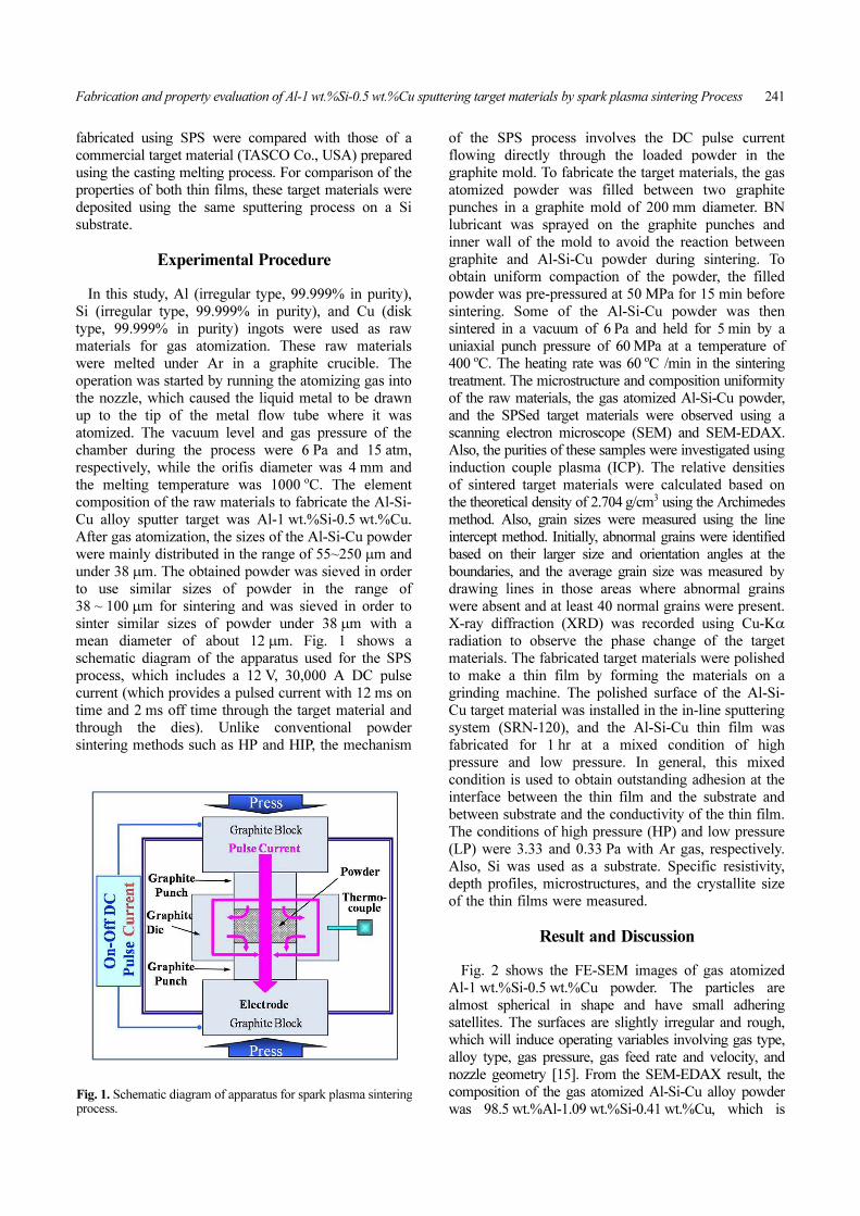
mean diameter of about 12 μm. Fig. 1 shows a
schematic diagram of the apparatus used for the SPS
process, which includes a 12 V, 30,000 A DC pulse
current (which provides a pulsed current with 12 ms on
time and 2 ms off time through the target material and
through the dies). Unlike conventional powder
sintering methods such as HP and HIP, the mechanism
of the SPS process involves the DC pulse current
flowing directly through the loaded powder in the
graphite mold. To fabricate the target materials, the gas
atomized powder was filled between two graphite
punches in a graphite mold of 200 mm diameter. BN
lubricant was sprayed on the graphite punches and
inner wall of the mold to avoid the reaction between
graphite and Al-Si-Cu powder during sintering. To
obtain uniform compaction of the powder, the filled
powder was pre-pressured at 50 MPa for 15 min before
sintering. Some of the Al-Si-Cu powder was then
sintered in a vacuum of 6 Pa and held for 5 min by a
uniaxial punch pressure of 60 MPa at a temperature of
400 oC. The heating rate was 60 oC /min in the sintering
treatment. The microstructure and composition uniformity
of the raw materials, the gas atomized Al-Si-Cu powder,
and the SPSed target materials were observed using a
scanning electron microscope (SEM) and SEM-EDAX.
Also, the purities of these samples were investigated using
induction couple plasma (ICP). The relative densities
of sintered target materials were calculated based on
the theoretical density of 2.704 g/cm3 using the Archimedes
method. Also, grain sizes were measured using the line
intercept method. Initially, abnormal grains were identified
based on their larger size and orientation angles at the
boundaries, and the average grain size was measured by
drawing lines in those areas where abnormal grains
were absent and at least 40 normal grains were present.
X-ray diffraction (XRD) was recorded using Cu-Kα
radiation to observe the phase change of the target
materials. The fabricated target materials were polished
to make a thin film by forming the materials on a
grinding machine. The polished surface of the Al-Si-
Cu target material was installed in the in-line sputtering
system (SRN-120), and the Al-Si-Cu thin film was
fabricated for 1 hr at a mixed condition of high
pressure and low pressure. In general, this mixed
condition is used to obtain outstanding adhesion at the
interface between the thin film and the substrate and
between substrate and the conductivity of the thin film.
The conditions of high pressure (HP) and low pressure
(LP) were 3.33 and 0.33 Pa with Ar gas, respectively.
Also, Si was used as a substrate. Specific resistivity,
depth profiles, microstructures, and the crystallite size
of the thin films were measured.
Result and Discussion
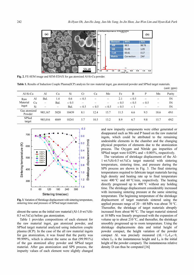
Fig. 2 shows the FE-SEM images of gas atomized
Al-1 wt.%Si-0.5 wt.%Cu powder. The particles are
almost spherical in shape and have small adhering
satellites. The surfaces are slightly irregular and rough,
which will induce operating variables involving gas type,
alloy type, gas pressure, gas feed rate and velocity, and
nozzle geometry [15]. From the SEM-EDAX result, the
composition of the gas atomized Al-Si-Cu alloy powder
was 98.5 wt.%Al-1.09 wt.%Si-0.41 wt.%Cu, which isFig. 1. Schematic diagram of apparatus for spark plasma sinteringprocess.
242 Ik-Hyun Oh, Jun-Ho Jang, Jun-Mo Yang, In-Jin Shon, Jae-Won Lim and Hyun-Kuk Park
almost the same as the initial raw material (Al-1.0 wt.%Si-
0.5 wt.%Cu) before gas atomization.
Table 1 provides compositions of each element for
the raw material ingot, gas atomized powder, and
SPSed target material analyzed using induction couple
plasma (ICP). In the case of the all raw material ingots
for gas atomization, it was found that the purity was
99.999%, which is almost the same as that (99.991%)
of the gas atomized alloy powder and SPSed target
material. After gas atomization and SPS process, the
impurity values of each element were slightly changed
and new impurity components were either generated or
disappeared such as Mo and P based on the raw material
ingots, which could be attributed to the remaining
undesirable elements in the chamber and the changing
physical properties of elements due to the atomization
process. The Oxygen and Nitride gas impurities of
SPSed target were 0.029% and < 0.005%, respectively.
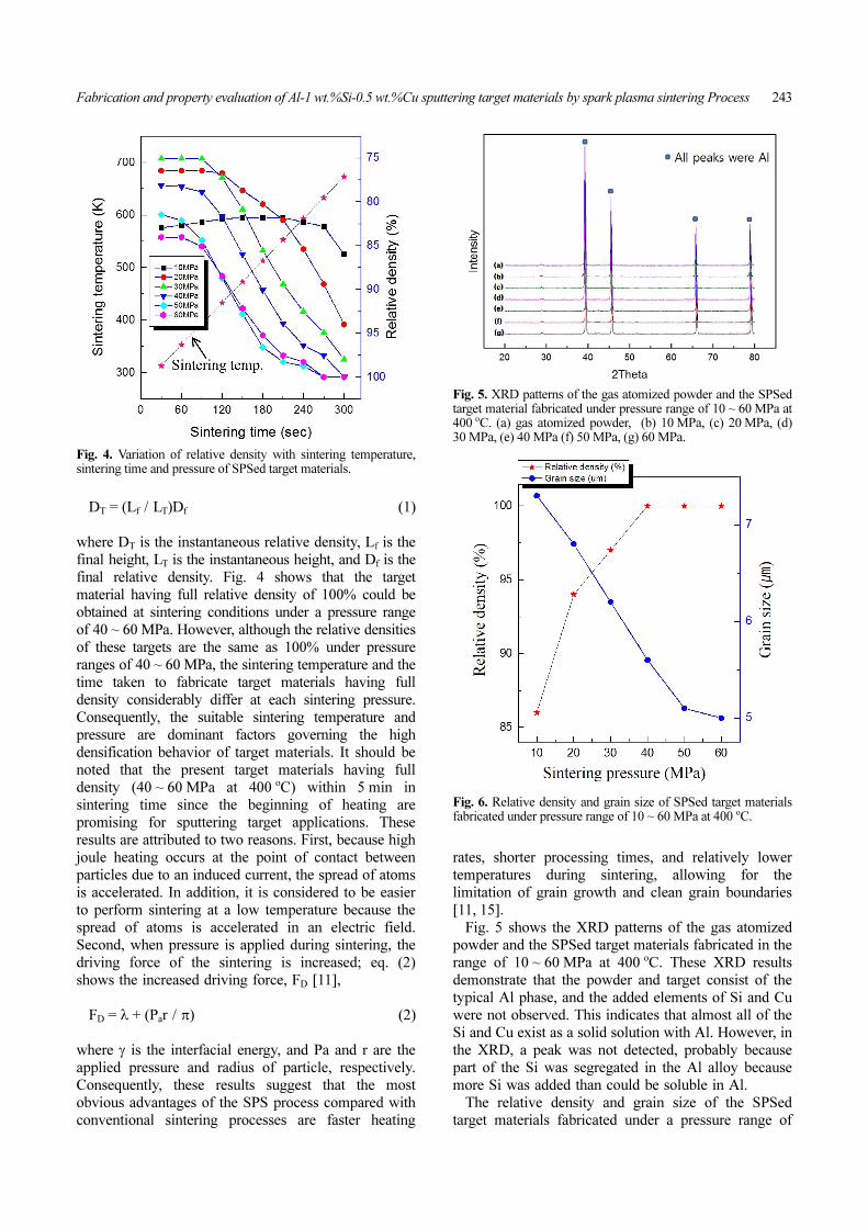
The variations of shrinkage displacement of the Al-
1 wt.%Si-0.5 wt.%Cu target material with sintering
temperature, sintering time, and pressure during the
SPS process are shown in Fig. 3. The final sintering
temperatures required to fabricate target materials having
high density and heating rate up to final temperature
were 400 oC and 60 oC/min, respectively. The heating
directly progressed up to 400 oC without any holding
time. The shrinkage displacement considerably increased
with increasing sintering pressure at the same sintering
temperature. The beginning temperature of the shrinkage
displacement of target materials sintered using the
applied pressure range of 20 ~ 60 MPa was about 70 oC.
Thereafter, the shrinkage of target materials abruptly
increased from about 90 oC. The target material sintered
at 10 MPa was linearly progressed with the expansion of
volume up to about 210 oC, and thereafter, the shrinkage
smoothly progressed up to room temperature. Using the
shrinkage displacements data and initial height of
powder compact, the height variation of the powder
compact ΔL was precisely measured (ΔL = Lr-L0< 0,
where LT is the instantaneous height and L0 is the initial
height of the powder compact). The instantaneous relative
density D can thus be computed [16]
Fig. 2. FE-SEM image and SEM-EDAX for gas atomized Al-Si-Cu powder.
Table 1. Results of Induction Couple Plasma(ICP) analysis for raw material ingot, gas atomized powder and SPSed target materials.
(unit: ppm)
Al-Si-Cu Al Cu Si Cr Ca Mo Fe B P Mn Purity
RawMaterial
ingot
Al Bal. 1.4 0.6 < 0.5 − − 2.1 < 0.5 − − 5N
Cu − Bal. < 0.5 − − − < 0.5 < 0.5 < 0.5 − 5N
Si − − Bal. < 0.5 < 0.5 < 0.5 < 0.5 < 1 − − 5N
Gas atomizedPowder
985,167 5020 10439 8.1 12.4 15.7 11.5 6.6 9.5 18.6 4N1
SPSedtarget
985,016 4849 10241 5.7 10.5 13.2 8.9 6.7 9.8 15.7 4N2
Fig. 3. Variation of Shrinkage displacement with sintering temperature,sintering time and pressure of SPSed target materials.
Fabrication and property evaluation of Al-1 wt.%Si-0.5 wt.%Cu sputtering target materials by spark plasma sintering Process 243
DT = (Lf / LT)Df (1)
where DT is the instantaneous relative density, Lf is the
final height, LT is the instantaneous height, and Df is the
final relative density. Fig. 4 shows that the target
material having full relative density of 100% could be
obtained at sintering conditions under a pressure range
of 40 ~ 60 MPa. However, although the relative densities
of these targets are the same as 100% under pressure
ranges of 40 ~ 60 MPa, the sintering temperature and the
time taken to fabricate target materials having full
density considerably differ at each sintering pressure.
Consequently, the suitable sintering temperature and
pressure are dominant factors governing the high
densification behavior of target materials. It should be
noted that the present target materials having full
density (40 ~ 60 MPa at 400 oC) within 5 min in
sintering time since the beginning of heating are
promising for sputtering target applications. These
results are attributed to two reasons. First, because high
joule heating occurs at the point of contact between
particles due to an induced current, the spread of atoms
is accelerated. In addition, it is considered to be easier
to perform sintering at a low temperature because the
spread of atoms is accelerated in an electric field.
Second, when pressure is applied during sintering, the
driving force of the sintering is increased; eq. (2)
shows the increased driving force, FD [11],
FD = λ + (Par / π) (2)
where γ is the interfacial energy, and Pa and r are the
applied pressure and radius of particle, respectively.
Consequently, these results suggest that the most
obvious advantages of the SPS process compared with
conventional sintering processes are faster heating
rates, shorter processing times, and relatively lower
temperatures during sintering, allowing for the
limitation of grain growth and clean grain boundaries
[11, 15].
Fig. 5 shows the XRD patterns of the gas atomized
powder and the SPSed target materials fabricated in the
range of 10 ~ 60 MPa at 400 oC. These XRD results
demonstrate that the powder and target consist of the
typical Al phase, and the added elements of Si and Cu
were not observed. This indicates that almost all of the
Si and Cu exist as a solid solution with Al. However, in
the XRD, a peak was not detected, probably because
part of the Si was segregated in the Al alloy because
more Si was added than could be soluble in Al.
The relative density and grain size of the SPSed
target materials fabricated under a pressure range of
Fig. 4. Variation of relative density with sintering temperature,sintering time and pressure of SPSed target materials.
Fig. 5. XRD patterns of the gas atomized powder and the SPSedtarget material fabricated under pressure range of 10 ~ 60 MPa at400 oC. (a) gas atomized powder, (b) 10 MPa, (c) 20 MPa, (d)30 MPa, (e) 40 MPa (f) 50 MPa, (g) 60 MPa.
Fig. 6. Relative density and grain size of SPSed target materialsfabricated under pressure range of 10 ~ 60 MPa at 400 oC.
244 Ik-Hyun Oh, Jun-Ho Jang, Jun-Mo Yang, In-Jin Shon, Jae-Won Lim and Hyun-Kuk Park
10 ~ 60 MPa at 400 oC are shown in Fig. 6. The full
densities of 100% were continuously maintained from
the applied pressure of 40 MPa at 400 oC, as mentioned
above. Also, the grain size decrease due to the increase
in sintering pressure would be associated with the fast
densification of powders during sintering. Although the
grain size of as-gas atomized powder used in the
present work was about 4.1 μm after sintering, it was
found that the growth of grain size did not significantly
occur after sintering.
Table 2 shows the resistivity values of commercial
and SPSed Al-1 wt.%Si-0.5 wt.% Cu thin film deposited
on a Si substrate. According to the detail process
conditions, Ar gas was first applied at an initial pressure
of 6.5 × 10⁻⁴ Pa. When the thin film was formed, the
pressure was progressed under mixed condition of high
pressure (3.33 Pa) and low pressure (0.33 Pa) for 1 hr at
room temperature. The scan size of the surface for thin
films was 5 μm and specific resistivity was calculated
from eq. (3) using the face resistance obtained by a 4
point probe.
ρ = L • R/A (3)
where ρ is specific resistivity, L is the length, and R and
A are the resistance and sectional area, respectively. The
specific resistivity of the SPSed thin film was very
similar to that of the film deposited using a target
fabricated using the casting melting process.
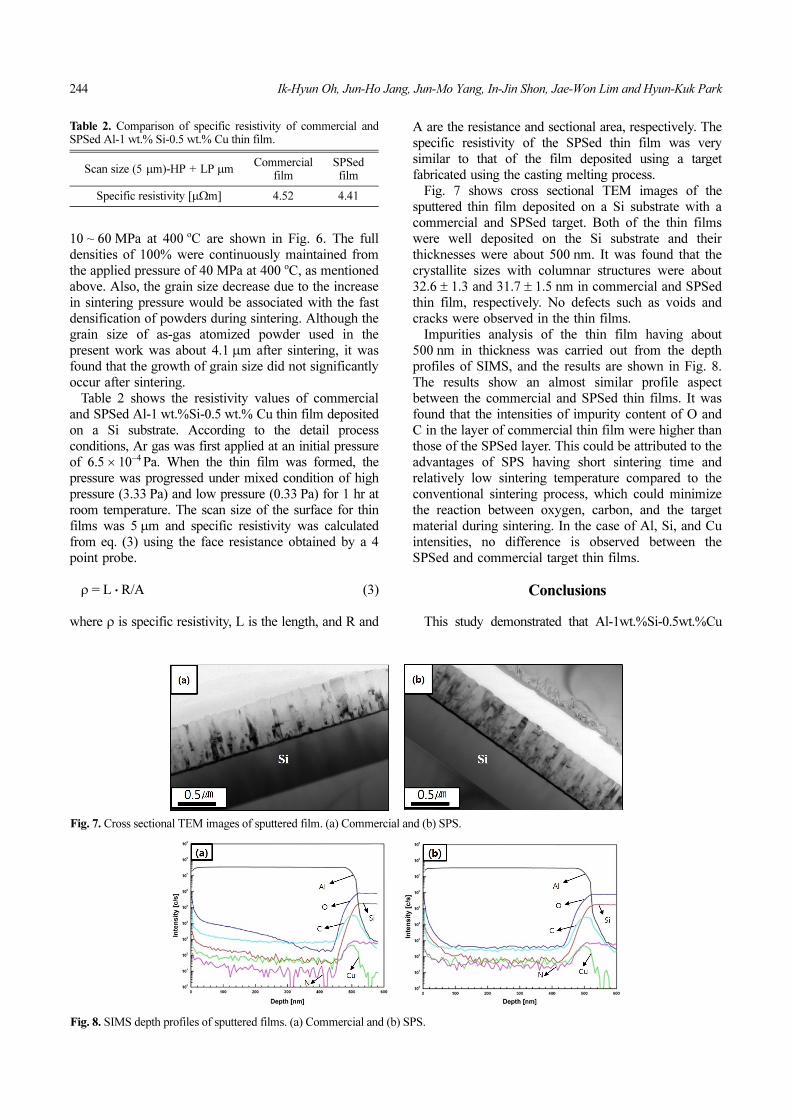
Fig. 7 shows cross sectional TEM images of the
sputtered thin film deposited on a Si substrate with a
commercial and SPSed target. Both of the thin films
were well deposited on the Si substrate and their
thicknesses were about 500 nm. It was found that the
crystallite sizes with columnar structures were about
32.6 ± 1.3 and 31.7 ± 1.5 nm in commercial and SPSed
thin film, respectively. No defects such as voids and
cracks were observed in the thin films.
Impurities analysis of the thin film having about
500 nm in thickness was carried out from the depth
profiles of SIMS, and the results are shown in Fig. 8.
The results show an almost similar profile aspect
between the commercial and SPSed thin films. It was
found that the intensities of impurity content of O and
C in the layer of commercial thin film were higher than
those of the SPSed layer. This could be attributed to the
advantages of SPS having short sintering time and
relatively low sintering temperature compared to the
conventional sintering process, which could minimize
the reaction between oxygen, carbon, and the target
material during sintering. In the case of Al, Si, and Cu
intensities, no difference is observed between the
SPSed and commercial target thin films.
Conclusions
This study demonstrated that Al-1wt.%Si-0.5wt.%Cu
Table 2. Comparison of specific resistivity of commercial andSPSed Al-1 wt.% Si-0.5 wt.% Cu thin film.
Scan size (5 μm)-HP + LP μmCommercial
filmSPSed film
Specific resistivity [μΩm] 4.52 4.41
Fig. 7. Cross sectional TEM images of sputtered film. (a) Commercial and (b) SPS.
Fig. 8. SIMS depth profiles of sputtered films. (a) Commercial and (b) SPS.

Fabrication and property evaluation of Al-1 wt.%Si-0.5 wt.%Cu sputtering target materials by spark plasma sintering Process 245
sputtering target using high purity powder obtained from
gas atomization process for semiconductor metallization
applications can be successfully fabricated using spark
plasma sintering method. From the study results, relatively
low temperature and shorter processing times allow the
sintering of Al-1wt.%Si-0.5wt.%Cu powder having full
density and high purity with little grain growth. The
properties of thin films deposited using the Al-
1 wt%Si-0.5 wt.%Cu target fabricated from SPS were
compared with those of the commercial target material
prepared using the casting melting process. From these
results, the properties of SPS thin films were almost
similar to the commercial thin films. Therefore, a high
quality SPSed sputtering target can be utilized as
sputtering target materials for the device interconnection
lines of a semiconductor.
Acknowledgments
This research was supported by an industrial source
technology research project from the Ministry of Trade,
Industry & Energy, Korea.
Reference
1. J. Sarkar, Sputtering targets and sputtered films for themicroelectronic industry, ISBN No.978-0-8155-1593-7(2014) 1-92.
2. J. Sarkar, Sputtering and thin film deposition, ISBNNo.978-0-8155-1593-7 (2014) 93-170.
3. J. Sarkar, Sputtering target manufacturing, ISBN No.978-0-8155-1593-7 (2014) 197-289.
4. Y. Y. Chen, J. C. Hus, C. Y. Lee, W. P. Wang, J. Mater. Sci.48 (2012) 1255-1230.
5. R. Bel Hadk Tahar, N. Bel Hadj Tahar, J. Am. Ceram. Soc.88 (2005) 1725-1728.
6. S, Bader, E.M. Kalaugher, E. Arzt, Thin Solid Film 263(1995) 75-184.
7. M.K. Mazumer, S. Yamamoto, H. Maeda, J. Komori. Y.Mashiko, Microelectr. Relat. 41 (2001) 1259-1264.
8. M. Zaborowski, P. Dumania, Microelectr. Eng. 50 (2000)301-309.
9. B. Kaouache, P. Gerguad, O. Thomas, O. Bostorm, M.Legros, Microelectr. Eng. 70 (2003) 447-454.
10. S. Dietrich, M. Schneegans, M. Moske, K. Smawer, Thinfilms 275 (1996) 159-163.
11. H. K. Park, J. H. Ryu, H. J. Youn, J. M. Yang, I. H. Oh,Mater. Trans. 53 (2012) 1056-1061.
12. H.C. Kim, I.J. Shon, Z.A. Munir, J. Mater. Sci. 40 (2005)2849-2854.
13. H.C. Kim, D.Y. Oh, I.J. Shon, Int. J. Ref. Met. Hard Mater.22 (2004) 197-203.
14. H.C. Kim, H.K. Park, I.K. Jung, I.Y. Ko, I.J. Shon, CermicsInt. 34 (2008) 1419-1423.
15. M. Ranmall, powder metallurgy science, ISBN No. 1-878954-42-3, 100-116.
16. M. Bernard-Granger, C. Huizard, J. Acta Mater. 55 (2007)3493-3504.