fabrication and characterisation of amorphous and nanocrystalline
TRANSCRIPT
Chapter 4
Fabrication and characterisation of amorphous and nanocrystalline Fe-Ni thin films
4.1 Introduction
4.2 Experiment
4.3 Results and Discussions
Co
nte
nts
4.4 Conclusion
4.1. Introduction
Nanocrystalline magnetic materials is increasingly becoming a hot topic of
research because of their potential in finding end uses in fields such as power
electronics, sensors, actuators, soft under layer for perpendicular recording media and
as the core material for write elements in the modern recording heads [39,83,84]. The
microstructure of these materials consists of nano sized ferromagnetic materials
embedded in an amorphous matrix. The matrix phase must also be ferromagnetic for
facilitating the exchange coupling between the nanoparticles. As a result of this
coupling, they often exhibit vanishing magnetocrystalline anisotropy. Since the soft
magnetic properties are strongly related to the crystalline anisotropy, the exchange
interaction in nanocrystalline magnetic materials results in an improvement of its soft
magnetic properties.
The averaging out of magnetocrystalline anisotropy in these materials can be
explained in terms of random anisotropy model proposed by Alben et al [66]. The
effective anisotropy energy density in this model is given by the square root of the
mean square fluctuation of the anisotropy energy in the exchange coupled volume.
Although the random anisotropy model was propounded to explain the magnetic
Chapter 4
80
softness in amorphous materials, Herzer showed that the model is also applicable to
nanocrystalline systems [67].
For an assembly of ferromagnetically coupled grains of size D (D < Lex) with
randomly oriented magnetocrystalline anisotropies K1, the average anisotropy <K> is
given by
( )nn
KA
DKK
−
⎟⎟⎟⎟⎟
⎠
⎞
⎜⎜⎜⎜⎜
⎝
⎛
⎟⎠⎞⎜
⎝⎛
>=<
42
21
1
1 [68] where n denotes the dimension of the
system. This means that <K> follows a 32
D , D2 and D6 dependence on grain size for
one-dimensional, two-dimensional and three dimensional structures, respectively. The
coercivity (Hc) and permeability ( µ ) are related to <K> through the relation
>∝< KHc and ><
∝K1µ .
The sensitive grain size dependence on the soft magnetic properties in these
materials is related to the interplay of local magnetocrystalline anisotropy energy and
the ferromagnetic exchange interaction. For large grains the magnetization can follow
the local easy magnetic directions and the magnetization process is determined by the
magnetocrystalline anisotropy K1 of the crystallites. However for very small grains, the
ferromagnetic exchange interaction forces the magnetic moments to align parallel to
each other. Thus the effective anisotropy will be an average over several grains and
will be reduced in magnitude. The dividing line between these two extremes is the
ferromagnetic exchange correlation length2
1
1⎟⎠⎞⎜
⎝⎛= K
ALex , where A is the exchange
stiffness constant and K1 is the anisotropy constant.
Amorphous alloys which are precursors of nanocrystalline materials can be
synthesized by a variety of techniques such as rapid solidification from the liquid state,
mechanical alloying, plasma processing and vapour deposition [1]. Nanocrystalline
Fabrication and characterisation of amorphous………
81
microstructure can be obtained by the controlled crystallization of the amorphous
state. There are several reports in the literature pertaining to this method of
preparation [85, 86, 2, 87]. Melt quenching or high energy ball milling was used for
preparing the metastable states and most of the studies were carried out in ribbons or
in powders. With the advent of nanocrystalline materials exhibiting excellent soft
magnetic properties thin films of these materials also auume significance from an
application point of view.
Vapour deposition offers a simple alternative for sputter deposition in
obtaining thin films of supersaturated solid solutions and other metastable states.
Amorphous magnetic thin films thus obtained presents high coercivity due to the
stresses in the films. One way of improving the magnetic softness is by precipitating
nanocrystals with in the amorphous matrix. Further, nanocrystallisation allows one to
tailor the magnetic properties by controlling the size of the precipitates. Control of
magnetic properties is highly essential in order to obtain miniaturized magnetic devices
with improved performance characteristics. Since the magnetic properties are strongly
dependent on the microstructure, the soft magnetic properties can be tuned by
modifying the microstructure.
Metglas 2826 MB (Fe40Ni38Mo4B18) is a soft magnetic alloy that exhibits
superior soft magnetic materials. Its softness after nanocrystallisation can be ascribed
to its two phase nature consisting of Fe-Ni nanocrystals embedded in the remaining
boron rich amorphous matrix. Additives like boron and molybdenum are incorporated
in the alloy to achieve specific objectives. Boron aids in retaining the glassy
characteristics while molybdenum is a known grain growth inhibitor. However, high
metalliod content causes deterioration not only in their magnetic properties but also in
elasticity and plasticity [61]. If B and Mo can be dispensed with in Fe-Ni based alloys
like Metglas, this brings in economy and is an attractive proposition from a
commercial point of view. Since Metglas is widely used for sensor applications, thin
Chapter 4
82
film form of this material would be of great interest for integrating thin film sensors
with today’s microelectronics. This can be realized by depositing thin films of this
material on suitable substrates.
Some attempts of preparation of Metglas thin films by thermal evaporation
have been reported in the literature [88, 70]. Thin films of Fe40Ni38Mo4B18 were
prepared by flash evaporation techniques [88]. The electron microscopy and
diffraction investigations on these films showed that the films decompose in a eutectic
fashion with thermal annealing. Magnetic studies were not carried out on these
samples and the main focus of the work was on the structural evolution of these films
with thermal annealing. An alloy film with the same composition was studied by
Hysen et al. [70]. Thin films (thickness around 36 nm) of Fe40Ni38Mo4B18 were
prepared by thermally evaporating Metglas 2826 MB ribbons. The deposited films
were amorphous and were thermally annealed to obtain nanocrystalline
microstructure. A lowering in crystallization temperature was observed (~473 K) when
compared to bulk alloy system (683 K) which was attributed to the lower volume
fraction of molybdenum in the thin films. The observed changes in coercivity with
annealing temperature were explained using random anisotropy model extended to
two dimensional systems. However in these investigations the composition of the film
was not ascertained and the nature of the microstructure were not established by any
experimental techniques. Such a study only will give credence in correlating the
microstructure with the magnetic properties. Also, the amorphous interlayer in
nanocrystalline magnetic material plays a crucial role in determining the magnetic and
electronic properties. Hence employment of sophisticated techniques like transmission
electron microscopy in characterizing the material has significance from an application
point of view. It is in this context that a systematic investigation on a magnetic soft
alloys based on Fe-Ni assumes relevance.
Fabrication and characterisation of amorphous………
83
The main objective of the work presented in this chapter is to gain an insight
into the microstructural evolution with thermal annealing in Fe-Ni based amorphous
thin films and to correlate the observed magnetic properties with microstructural
evolution. For this, Fe-Ni based amorphous thin films were prepared by thermal
evaporation technique. Nanocrystalline microstructure was obtained by the partial
crystallization of the amorphous films. Microstructure was controlled by annealing the
films at different temperatures. The films were characterized using x-ray diffraction
technique (XRD), transmission electron microscopy (TEM), selected area electron
diffraction (SAED), Energy Dispersive x-ray Spectrometry (EDS), x-ray photoelectron
spectroscopy (XPS) and vibrating sample magnetometer. Finally the grain size
dependence of coercivity is explained using random anisotropy model extended to two
dimensional systems.
4.2. Experiment
4.2.1 Preparation
Commercially available Metglas 2826 MB ribbon of composition
Fe40Ni38Mo4B18 was employed as a source material to deposit Fe-Ni thin films on
silicon, glass and NaCl substrates. The silicon and glass substrates were cleaned with
acetone, ethanol and trichloroethylene and were immediately loaded into the vacuum
chamber. The distance from source to the centre of 1 cm2 substrate was 20 cm. The
films were deposited by thermal evaporation using a current of 23 A at a pressure of
about 1x10⁻⁵ mbar. The base pressure of ~ 1x10⁻⁵ m bar was achieved by a diffusion
pump backed with a rotary pump. These thin films have also been heat treated at 373
K, 473 K, 573 K and 673 K to follow microstructural evolution of the as deposited
films. The annealing treatment consisted of increasing the temperature of the samples
at about 10 K /minute to the desired temperature, holding it for 1 hr and cooling to
room temperature. The annealing was performed in a vacuum of 1x 10⁻⁵ mbar.
Chapter 4
84
4.2.2 Characterization
The thicknesses of the films were determined using scanning electron
microscopy cross-sectional measurements (JOEL JSM 6390). X-ray diffraction
measurements were performed using an x-ray powder diffractometer technique
employing a copper target (Cu Kα = 1.5418 A0, Rigaku Dmax C). The scanning speed
was adjusted to 20min−1 with a sampling interval of 0.05. Transmission electron
microscopy experiments were carried out on films coated on NaCl substrates. A Joel
JEM-2200 FS electron microscope operated at 200 kV was used for this. The
compositions of the films were analyzed using an energy dispersive x-ray spectrometer
which was attached to the TEM column. STM studies were carried out using a Veeco-
Digital Instruments multimode scanning probe microscope operated under ambient
conditions. The measurements were performed using tungsten tips. The STM images
were recorded in the constant current mode at a sample bias of 1.2V and a current set
point of 0.4 nA. The topographical images represent the height of the tunnelling tip
above the sample. The images are digitally filtered to remove the low frequency noises.
X-ray photoelectron spectroscopy (XPS) measurements were carried out using an
Omicron Nanotechnology Multiprobe Instrument. XPS spectra were obtained using a
high resolution hemisphere analyzer EA 125 HR equipped with a detection system
consisting of seven channeltrons. A monochromated Al Kα source of energy hν =
1486.6 eV was used to probe the films which was attached to a molybdenum sample
holder. Pressure in the XPS chamber during the measurements was 5 × 10⁻¹⁰ mbar.
Room temperature magnetization measurements were carried out using a vibrating
sample magnetometer (DMS 1660 VSM) with an external field varying from −1 to +1
kOe.
Fabrication and characterisation of amorphous………
85
4.3 Results and discussions
4.3.1 Composition analysis
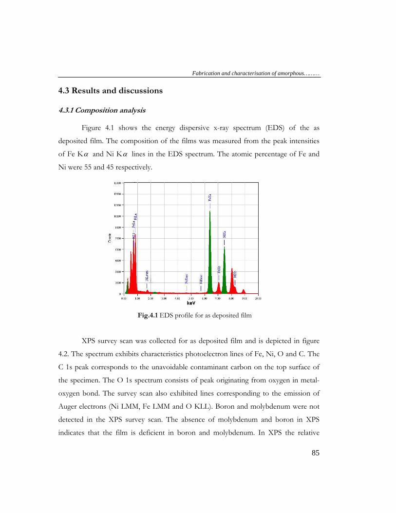
Figure 4.1 shows the energy dispersive x-ray spectrum (EDS) of the as
deposited film. The composition of the films was measured from the peak intensities
of Fe Kα and Ni Kα lines in the EDS spectrum. The atomic percentage of Fe and
Ni were 55 and 45 respectively.
Fig.4.1 EDS profile for as deposited film
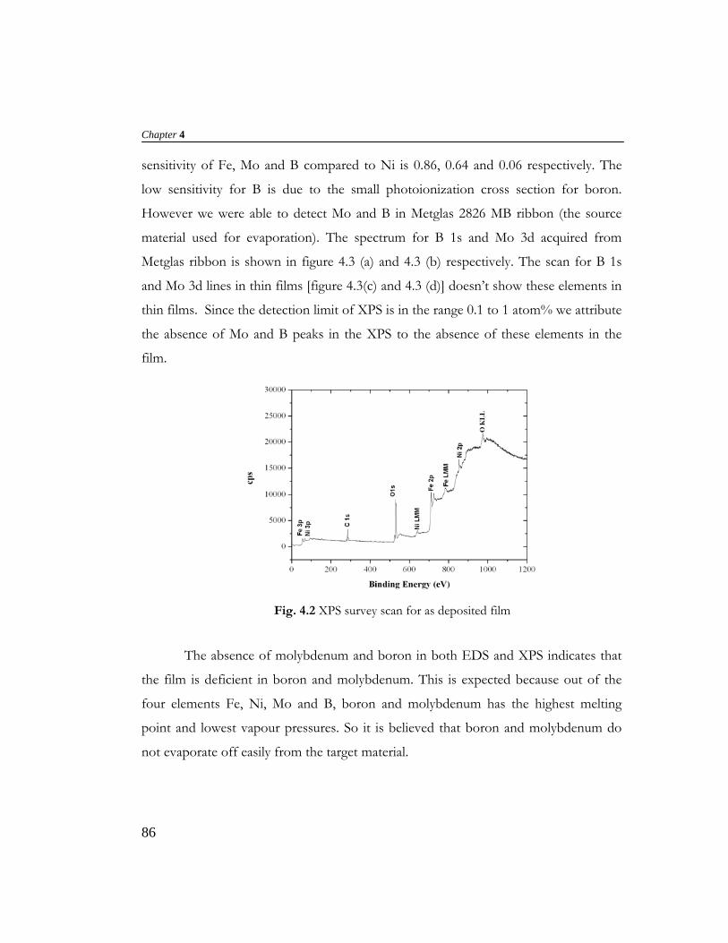
XPS survey scan was collected for as deposited film and is depicted in figure
4.2. The spectrum exhibits characteristics photoelectron lines of Fe, Ni, O and C. The
C 1s peak corresponds to the unavoidable contaminant carbon on the top surface of
the specimen. The O 1s spectrum consists of peak originating from oxygen in metal-
oxygen bond. The survey scan also exhibited lines corresponding to the emission of
Auger electrons (Ni LMM, Fe LMM and O KLL). Boron and molybdenum were not
detected in the XPS survey scan. The absence of molybdenum and boron in XPS
indicates that the film is deficient in boron and molybdenum. In XPS the relative
Chapter 4
86
sensitivity of Fe, Mo and B compared to Ni is 0.86, 0.64 and 0.06 respectively. The
low sensitivity for B is due to the small photoionization cross section for boron.
However we were able to detect Mo and B in Metglas 2826 MB ribbon (the source
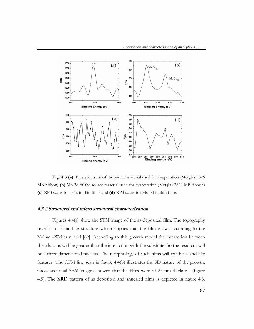
material used for evaporation). The spectrum for B 1s and Mo 3d acquired from
Metglas ribbon is shown in figure 4.3 (a) and 4.3 (b) respectively. The scan for B 1s
and Mo 3d lines in thin films [figure 4.3(c) and 4.3 (d)] doesn’t show these elements in
thin films. Since the detection limit of XPS is in the range 0.1 to 1 atom% we attribute
the absence of Mo and B peaks in the XPS to the absence of these elements in the
film.
Fig. 4.2 XPS survey scan for as deposited film
The absence of molybdenum and boron in both EDS and XPS indicates that
the film is deficient in boron and molybdenum. This is expected because out of the
four elements Fe, Ni, Mo and B, boron and molybdenum has the highest melting
point and lowest vapour pressures. So it is believed that boron and molybdenum do
not evaporate off easily from the target material.
Fabrication and characterisation of amorphous………
87
Fig. 4.3 (a) B 1s spectrum of the source material used for evaporation (Metglas 2826
MB ribbon) (b) Mo 3d of the source material used for evaporation (Metglas 2826 MB ribbon)
(c) XPS scans for B 1s in thin films and (d) XPS scans for Mo 3d in thin films
4.3.2 Structural and micro structural characterization
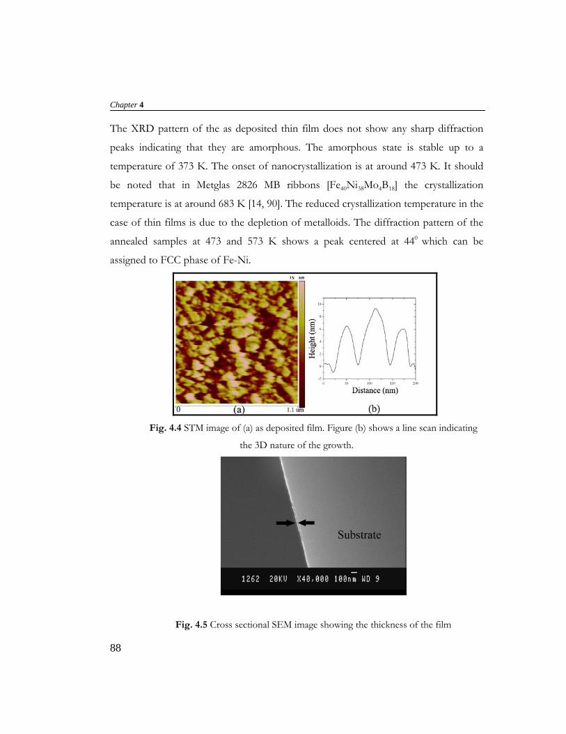
Figures 4.4(a) show the STM image of the as-deposited film. The topography
reveals an island-like structure which implies that the film grows according to the
Volmer–Weber model [89]. According to this growth model the interaction between
the adatoms will be greater than the interaction with the substrate. So the resultant will
be a three-dimensional nucleus. The morphology of such films will exhibit island-like
features. The AFM line scan in figure 4.4(b) illustrates the 3D nature of the growth.
Cross sectional SEM images showed that the films were of 25 nm thickness (figure
4.5). The XRD pattern of as deposited and annealed films is depicted in figure 4.6.
Chapter 4
88
The XRD pattern of the as deposited thin film does not show any sharp diffraction
peaks indicating that they are amorphous. The amorphous state is stable up to a
temperature of 373 K. The onset of nanocrystallization is at around 473 K. It should
be noted that in Metglas 2826 MB ribbons [Fe40Ni38Mo4B18] the crystallization
temperature is at around 683 K [14, 90]. The reduced crystallization temperature in the
case of thin films is due to the depletion of metalloids. The diffraction pattern of the
annealed samples at 473 and 573 K shows a peak centered at 440 which can be
assigned to FCC phase of Fe-Ni.
Fig. 4.4 STM image of (a) as deposited film. Figure (b) shows a line scan indicating
the 3D nature of the growth.
Fig. 4.5 Cross sectional SEM image showing the thickness of the film
Fabrication and characterisation of amorphous………
89
Fig. 4.6 XRD pattern of (a) as deposited film and films annealed at (b) 373 K (c) 473 K
and (d) 573 K
Fig. 4.7 TEM bright field image of (a) as deposited film and films annealed at (b) 473 K
(c) 573 K and (d) 673 K. The arrow in (d) points to the nanocrystalline precipitates
Chapter 4
90
The as deposited and annealed films were also investigated by TEM. Figure 4.7
(a) shows the bright field image of the as deposited thin films. The microstructure
exhibits a contrast typical of an amorphous material.
The electron diffraction pattern (figure 4.9(a)) consists of a wide diffraction
ring corresponding to an inter-planar distance d = 2.014 A0. This corresponds to an
average distance ( xm ) between atoms in the amorphous structure, where xm =
1.23d=2.5 A0. This value is in agreement with the observations of Dunlop et al [91] in
Finemet alloys.
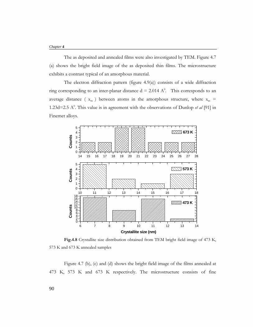
Fig.4.8 Crystallite size distribution obtained from TEM bright field image of 473 K,
573 K and 673 K annealed samples
Figure 4.7 (b), (c) and (d) shows the bright field image of the films annealed at
473 K, 573 K and 673 K respectively. The microstructure consists of fine
6 7 8 9 10 11 12 13 1402468
1012141618
Cou
nts
Crystallite size (nm)
473 K
14 15 16 17 18 19 20 21 22 23 24 25 26 27 28012345
Cou
nts
673 K
10 11 12 13 14 15 16 17 18012345
Cou
nts 573 K
Fabrication and characterisation of amorphous………
91
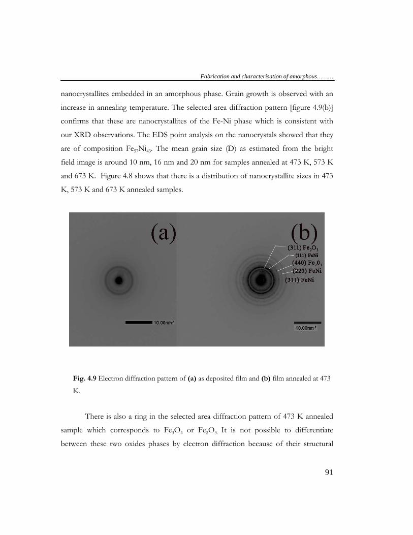
nanocrystallites embedded in an amorphous phase. Grain growth is observed with an
increase in annealing temperature. The selected area diffraction pattern [figure 4.9(b)]
confirms that these are nanocrystallites of the Fe-Ni phase which is consistent with
our XRD observations. The EDS point analysis on the nanocrystals showed that they
are of composition Fe57Ni43. The mean grain size (D) as estimated from the bright
field image is around 10 nm, 16 nm and 20 nm for samples annealed at 473 K, 573 K
and 673 K. Figure 4.8 shows that there is a distribution of nanocrystallite sizes in 473
K, 573 K and 673 K annealed samples.
Fig. 4.9 Electron diffraction pattern of (a) as deposited film and (b) film annealed at 473
K.
There is also a ring in the selected area diffraction pattern of 473 K annealed
sample which corresponds to Fe3O4 or Fe2O3. It is not possible to differentiate
between these two oxides phases by electron diffraction because of their structural
Chapter 4
92
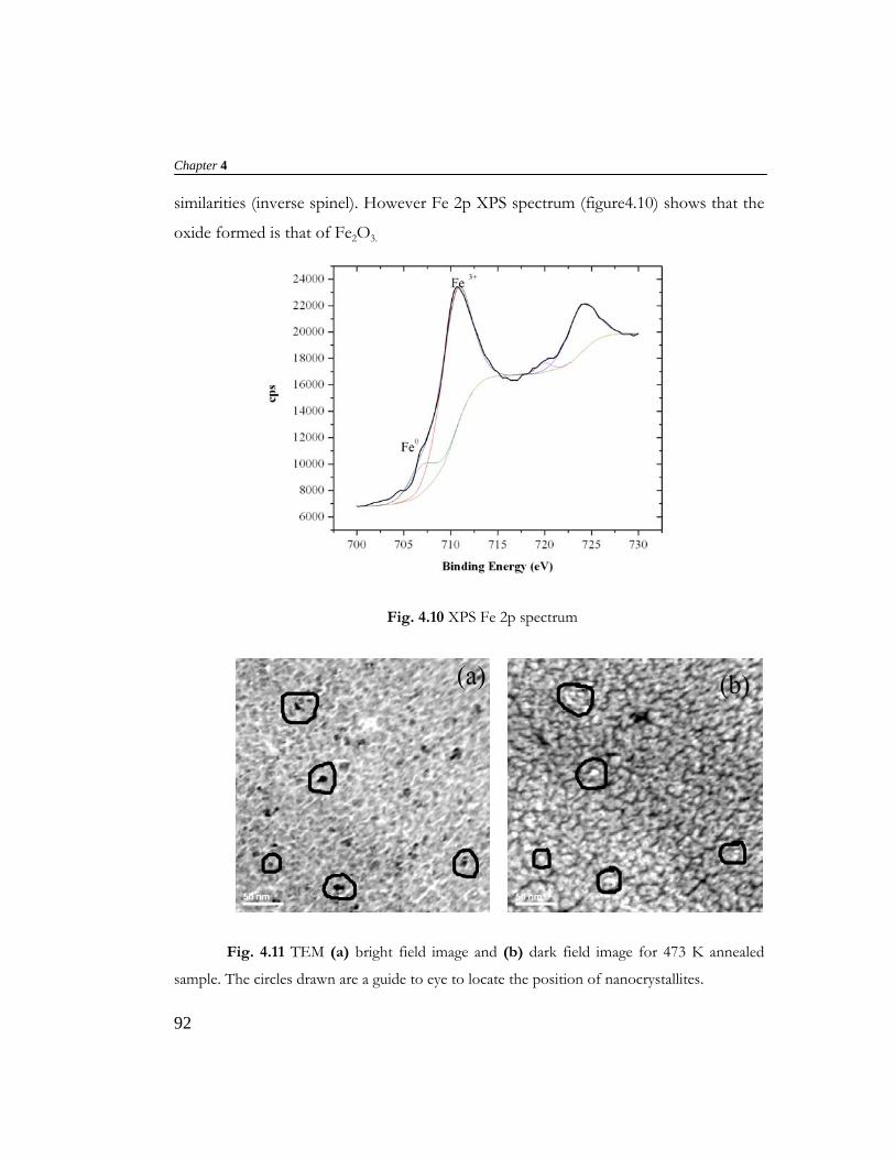
similarities (inverse spinel). However Fe 2p XPS spectrum (figure4.10) shows that the
oxide formed is that of Fe2O3.
Fig. 4.10 XPS Fe 2p spectrum
Fig. 4.11 TEM (a) bright field image and (b) dark field image for 473 K annealed
sample. The circles drawn are a guide to eye to locate the position of nanocrystallites.
Fabrication and characterisation of amorphous………
93
The Fe 2p3/2 peak occurs at around 710 eV which indicates the presence of
Fe2O3 on the surface of the film. Curve fitting shows that Fe 2p peak can be resolved
into two components with binding energies centered at 710 and 707 eV which
corresponds to Fe3+ and Fe0 respectively [92]. The absence of oxide peaks in the XRD
pattern implies that their percentage concentration is very low and is well below the
detection limits of XRD. Since we were not employing any capping agents against
oxidation the formation native oxide layer on the surface of the films cannot be ruled
out.
The presence of nanocrystals in an amorphous matrix is further evident from
the TEM dark field image shown in figure 4.11 (b). In bright field imaging we are
probing the electrons which have traversed the specimen without significant change in
direction. Hence we cannot distinguish the contrast changes due to thickness variation
or due to the presence of crystallites. Dark field imaging is more informative because it
uses deflected electrons rather than the transmitted ones for forming images. In dark
field imaging one is using the electrons which have actually interacted with the
specimen. The dark field image in figure 4.11(b) shows the coexistence of both
amorphous and crystalline phases in 473 K annealed samples.
4.3.3 Magnetic studies
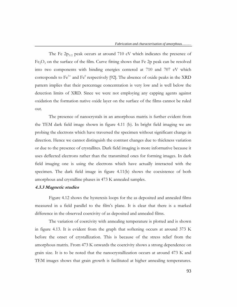
Figure 4.12 shows the hysteresis loops for the as deposited and annealed films
measured in a field parallel to the film’s plane. It is clear that there is a marked
difference in the observed coercivity of as deposited and annealed films.
The variation of coercivity with annealing temperature is plotted and is shown
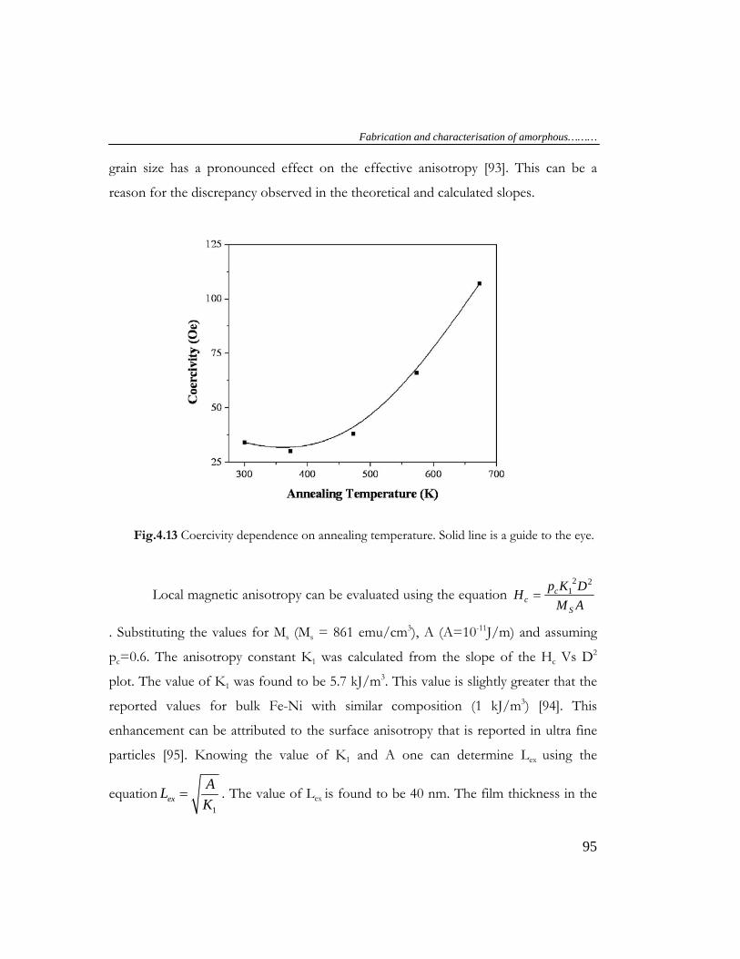
in figure 4.13. It is evident from the graph that softening occurs at around 373 K
before the onset of crystallization. This is because of the stress relief from the
amorphous matrix. From 473 K onwards the coercivity shows a strong dependence on
grain size. It is to be noted that the nanocrystallization occurs at around 473 K and
TEM images shows that grain growth is facilitated at higher annealing temperatures.
Chapter 4
94
The coercivity increased from 36 Oe to 107 Oe as the grain size increased from 10 to
20 nm.
Fig. 4.12 Room temperature hysteresis loop of (a) as deposited and films annealed at (b)
473 K (c) 573 K and (d) 673 K measured in a parallel field
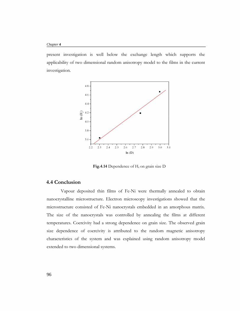
The coercivity in nanocrystalline ferromagnetic films can also be described by the
random anisotropy model extended to two dimensional systems [ref Chapter 2].
The experimental dependence of Hc on grain size, D is shown in figure 4.14. Solid line
is a linear fit to the experimental points. The slope of the curve was found to be ~1.5.
One can notice that there is a discrepancy in the value of calculated and theoretical
slopes. It should be noted that while deriving the D2 law a single value for the grain
size D was assumed. But the size distribution chart from the electron micrographs
(figure 4.8) show that there is a distribution in grain size, D. The inhomogeneity in the
Fabrication and characterisation of amorphous………
95
grain size has a pronounced effect on the effective anisotropy [93]. This can be a
reason for the discrepancy observed in the theoretical and calculated slopes.
Fig.4.13 Coercivity dependence on annealing temperature. Solid line is a guide to the eye.
Local magnetic anisotropy can be evaluated using the equation AMDKpH
S
cc
221=
. Substituting the values for Ms (Ms = 861 emu/cm3), A (A=10-11J/m) and assuming
pc=0.6. The anisotropy constant K1 was calculated from the slope of the Hc Vs D2
plot. The value of K1 was found to be 5.7 kJ/m3. This value is slightly greater that the
reported values for bulk Fe-Ni with similar composition (1 kJ/m3) [94]. This
enhancement can be attributed to the surface anisotropy that is reported in ultra fine
particles [95]. Knowing the value of K1 and A one can determine Lex using the
equation1
exALK
= . The value of Lex is found to be 40 nm. The film thickness in the
Chapter 4
96
present investigation is well below the exchange length which supports the
applicability of two dimensional random anisotropy model to the films in the current
investigation.
Fig.4.14 Dependence of Hc on grain size D
4.4 Conclusion
Vapour deposited thin films of Fe-Ni were thermally annealed to obtain
nanocrystalline microstructure. Electron microscopy investigations showed that the
microstructure consisted of Fe-Ni nanocrystals embedded in an amorphous matrix.
The size of the nanocrystals was controlled by annealing the films at different
temperatures. Coercivity had a strong dependence on grain size. The observed grain
size dependence of coercivity is attributed to the random magnetic anisotropy
characteristics of the system and was explained using random anisotropy model
extended to two dimensional systems.
Chapter 5
Swift heavy ion induced surface modification for tailoring coercivity in Fe-Ni based amorphous thin films.
5.1 Introduction 5.2 Experiment 5.3 Results 5.4 Discussions
Co
nte
nts
5.5 Conclusion
5.1. Introduction
Fe-Ni based amorphous thin films are increasingly becoming an interesting
topic of research because of their potential applications in soft magnetic devices [1, 39,
84, 96, and 97]. Metallic alloys with disordered structure are produced from the liquid
state during cooling and are also known as metallic glasses [98]. There are several
methods in vogue for the preparation of amorphous alloys. Here, physical vapour
deposition, high energy ball milling, ion beam irradiation and melt spinning needs
special mention.
Control of magnetic properties is highly essential in order to obtain
miniaturized magnetic devices with improved performance characteristics. The
magnetic properties are strongly dependent on the microstructure and hence the
magnetic properties of these materials can be tailored by modifying the microstructure.
For example, the variation in the sputtering rate during the sputter deposition of
magnetic thin films can result in the modification of coercivity [29]. Coercivity of
magnetic thin films can also be tailored by depositing films on seed layers [99].
Recently, the modification of the magnetic properties in Fe based nanocrystalline
Chapter 5
98
alloys by thermal annealing was reported [69]. In thin magnetic films, the surface
roughness plays an important role in the magnetization reversal mechanisms and this
in turn determines the coercivity of the material [100,101].
Ion irradiation has been considered as an alternative tool to modify the surface
properties. An energetic ion that penetrates a solid loses energy mainly via two
independent process: (a) electronic excitation and ionization [electronic energy loss,
(dE/dx)e ] which is dominant in the high energy regime (greater than 1MeV/ nucleon)
and (b) elastic collisions with nuclei of the target atoms [ nuclear energy loss (dE/dx)n ]
which are dominant in the low energy regime. The ion energy loss per unit path length
depends strongly on the ion velocity. Swift heavy ion passes through a solid with a
velocity comparable to the Bohr velocity of electrons and loses its energy while
traversing through the material. The rapid energy transfer during the inelastic collision
results in a transient excitation of the medium that finally culminates in the production
of point defects, clusters, columnar defects and phase transformation along the path
of the heavy ion beam [102-106].
The mechanism by which the energy can be deposited is through two different
process, namely thermal spike and coulomb explosion [107-109]. In the former the ion
beam excites the electronic system at the local site and electrons transfer this energy to
phonons via electron-phonon coupling resulting in an increase in the local
temperature. In the latter, ions create ionization zones during their passage through
the material. The ionization zone with positive charges may explode under
electrostatic force and induces strain in the material.
Metallic glasses were thought of resistant to irradiation induced modifications.
This hypothesis was based on the fact that irradiation induced disorder is easily
absorbed in the heavily disordered structure of an amorphous system. But in the 1980s
it was observed that metallic glasses when subjected to irradiation produced damages
[110,111]. Glassy alloys like Pd80Si20 and Cu50Zr50 when irradiated with high energy ions
Swift heavy ion induced surface modification………
99
were found to be undergoing dimensional changes perpendicular to the ion beam,
whereas the sample shrunk in dimension parallel to the ion beam. Measurements using
x-ray diffraction and electrical resistivity revealed that the structural modifications of
radiation deformed samples were small in comparison to the dimensional changes.
This discovery was rather surprising because of the following: (1) At that time there
was a supposition that a metallic glass, as a completely disordered metal, would be
more radiation resistant than any crystalline metal (2) In crystalline materials any
radiation induced anisotropic change in sample dimensions are due to a natural
crystallographic anisotropy. In sharp contrast, dimensional changes in glassy Pd80Si20
and Cu50Zr50 was introduced by the beam itself and (3) the number of atoms, which
occupied new positions in order to accomodate the dimensional changes exceeded by
one or two orders of magnitude than the number of atoms which are displaced via the
nuclear energy loss.
Later on, the anisotropic growths in metallic glasses were experimentally
evidenced by many researchers [112,113]. Audouard et al [112] observed that the
irradiation of Fe85B15 ribbons with 850 MeV 207Pb and 350 MeV 238U results in the
formation of hillocks and hollows. The formation of hillocks was attributed to the
damage created in individual ion tracks and hollows were linked to the occurrence of
anisotropic growth phenomenon. Later on, FeBSiC and Fe55Zr45 ribbons were
subjected to investigate the role of linear rate of electronic excitation (dE/dx)e and
temperature on defect creation and growth process [113]. Contrary to the earlier belief
that the effect of swift heavy ion on metallic glasses was limited to the anisotropic
growth, Dunlop et al. in 2003 showed that partial crystallization of an amorphous
alloy (FINEMET) is also possible by a high level of electronic energy deposition [91].
This crystallization phenomenon was interpreted in terms of an irradiation induced
pressure wave which allowed a rearrangement of the local atomic structure of the
alloy. These findings lead to the conviction that electronic excitation could induce
Chapter 5
100
structural modification in metallic glasses and also macroscopic variations in the
dimensions of irradiated metallic glass should induce modifications of the topography
of the sample surface.
Fe40Ni38Mo8B14 (Metglas 2826) is an amorphous alloy which shows superior
soft magnetic properties [114-115]. Since Metglas is widely used for sensor
applications, thin film form of this material would be of great interest for integrating
thin film sensors with today’s microelectronics. This can be realized by depositing thin
films of this material on suitable substrates.
The surface evolution of a thin film under swift heavy ion irradiation will be an
outcome of a competition between sputtering induced surface roughening process and
the material transport induced smoothening process. The final film morphology thus
depends on the dominant process. Mayr and Averback [116] observed that the
smoothening of a rough amorphous film occured during ion beam irradiation and
radiation induced viscous flow was identified as the dominant surface relaxation
mechanism. Mieskes et al. [117] observed an increase in surface roughness in Au, Zr,
Ti when irradiated with 230 MeV Au ions. The increased surface roughness was
attributed to the sputtering induced by Swift heavy ions. The magnetic properties of
thin films are strongly dependent on the surface/interface roughness and SHI is an
effective tool in modifying the surface of a material.
Considering the prospects of fabricating thin films based on Fe-Ni from
metallic glass ribbons by simple vacuum evaporation techniques and the fact that
amorphous alloys are not resistant to irradiation induced damages, a detailed
investigation in probing the surface modification of amorphous thin films of Fe-Ni is
worthwhile. It was thought that swift heavy ions would modify the surface structure of
these alloys and will eventually lead to modification of magnetic properties. Further,
the studies relating to SHI induced surface modifications and the intrinsic magnetic
properties of thin films are rather scarce or seldom reported. The impingement of ions
Swift heavy ion induced surface modification………
101
with different fluence on the alloy is bound to produce systematic microstructural
changes and if these changes produce a pattern, this could effectively be used for
tailoring the coercivity of these materials. The in situ method of tailoring coercivity
using swift heavy ion is novel and is an ingenious tool in creating surface modification
which will eventually lead to changes in the bulk property. AFM is a promising tool
for such a study on ion bombarded films where a minimum sample preparation is
required. It offers a good lateral resolution too. The present study was carried out in
order to investigate the effect of swift heavy ion irradiation on the magnetic and
surface properties of Fe-Ni based amorphous alloys. Attempts are made to correlate
the observed magnetic properties with surface evolution.
5.2. Experiment
Fe-Ni films with a thickness of 35 nm were deposited using a composite target
having the composition Fe40Ni38Mo8B14 (Metglas 2826) onto ultrasonically cleaned
glass substrates employing thermal evaporation techniques. During deposition the
base pressure in the chamber was maintained at 1x10⁻⁵ mbar with the help of a
diffusion pump backed with a rotary pump. These samples were irradiated by 108
MeV Ag8+ ions at room temperature with different fluences ranging from 1x10¹² to
3x10¹³ ions cm-2 using a 15 UD Pelletron accelerator at Inter University Accelerator
Centre, New Delhi, India. A uniform irradiation over an area of 1x1 cm2 was achieved
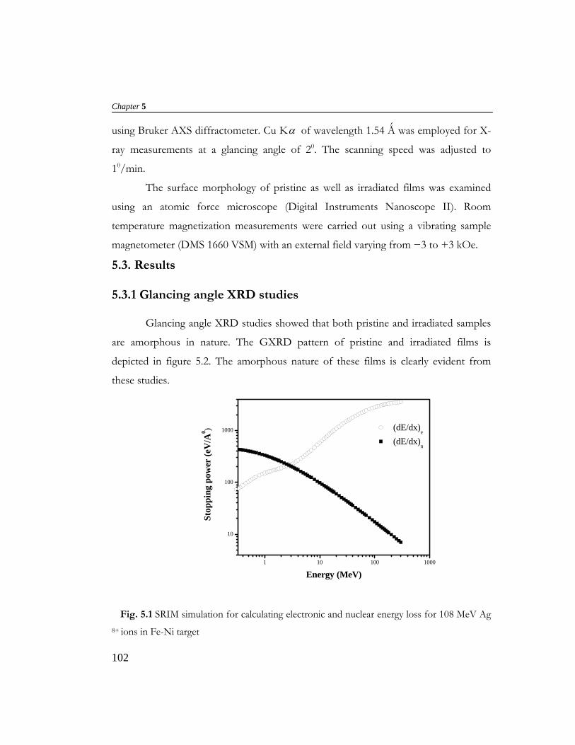
using a raster scanner. With the computer code SRIM, the nuclear stopping power
(dE/dx)n , electronic stopping power (dE/dx)e and the residual range Rp were calculated
as a function of ion energy. The value of (dE/dx)e is close to 28 keV/nm and are
greater than the corresponding (dE/dx)n values (1.6 eV/nm) [figure 5.1] . The
projected range of 108 MeV silver ions (Rp= 7 mµ ) is higher than the film thickness so
that the ion beam traverses through the material thickness and finally gets deposited in
the substrate. The films were subjected to x-ray diffraction (XRD) at grazing incidence
Chapter 5
102
using Bruker AXS diffractometer. Cu Kα of wavelength 1.54 Ǻ was employed for X-
ray measurements at a glancing angle of 20. The scanning speed was adjusted to
10/min.
The surface morphology of pristine as well as irradiated films was examined
using an atomic force microscope (Digital Instruments Nanoscope II). Room
temperature magnetization measurements were carried out using a vibrating sample
magnetometer (DMS 1660 VSM) with an external field varying from −3 to +3 kOe.
5.3. Results
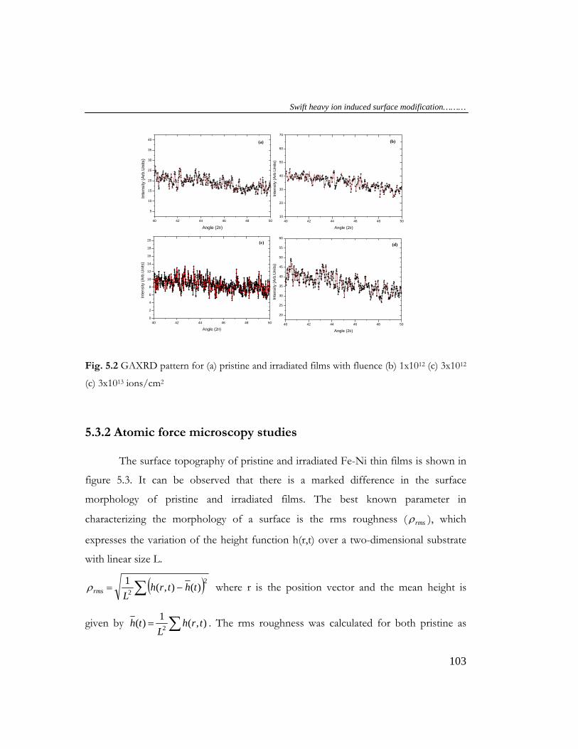
5.3.1 Glancing angle XRD studies
Glancing angle XRD studies showed that both pristine and irradiated samples
are amorphous in nature. The GXRD pattern of pristine and irradiated films is
depicted in figure 5.2. The amorphous nature of these films is clearly evident from
these studies.
1 10 100 1000
10
100
1000
Stop
ping
pow
er (e
V/A
0 )
Energy (MeV)
(dE/dx)e
(dE/dx)n
Fig. 5.1 SRIM simulation for calculating electronic and nuclear energy loss for 108 MeV Ag 8+ ions in Fe-Ni target
Swift heavy ion induced surface modification………
103
40 42 44 46 48 50
5
10
15
20
25
30
35
40
40 42 44 46 48 50
20
25
30
35
40
45
50
55
60
40 42 44 46 48 5010
20
30
40
50
60
70
40 42 44 46 48 500
2
4
6
8
10
12
14
16
18
20
(a)
Inte
nsity
(Arb
.Uni
ts)
Angle (2θ)
(d)
Inte
nsity
(Arb
.Uni
ts)
Angle (2θ)
(b)
Inte
nsity
(Arb
.Uni
ts)
Angle (2θ)
(c)
Inte
nsity
(Arb
.Uni
ts)
Angle (2θ)
Fig. 5.2 GAXRD pattern for (a) pristine and irradiated films with fluence (b) 1x10¹² (c) 3x10¹²
(c) 3x10¹³ ions/cm2
5.3.2 Atomic force microscopy studies
The surface topography of pristine and irradiated Fe-Ni thin films is shown in
figure 5.3. It can be observed that there is a marked difference in the surface
morphology of pristine and irradiated films. The best known parameter in
characterizing the morphology of a surface is the rms roughness ( rmsρ ), which
expresses the variation of the height function h(r,t) over a two-dimensional substrate
with linear size L.
( )∑ −=2
2 )(),(1 thtrhLrmsρ where r is the position vector and the mean height is
given by ∑= ),(1)( 2 trhL
th . The rms roughness was calculated for both pristine as
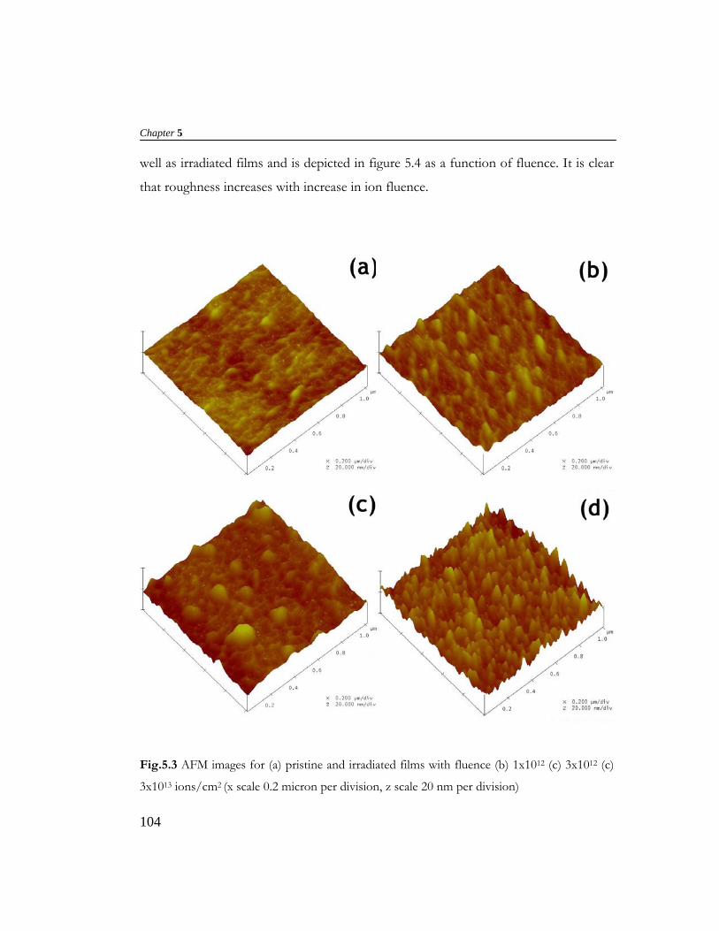
Chapter 5
104
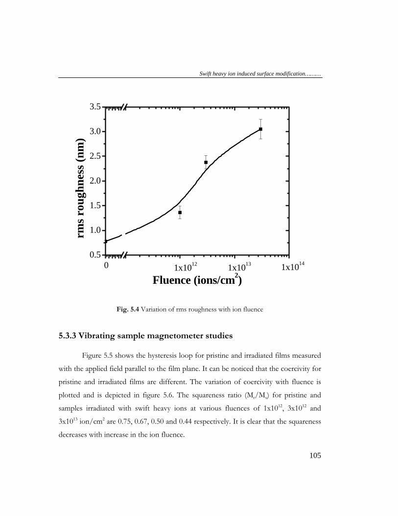
well as irradiated films and is depicted in figure 5.4 as a function of fluence. It is clear
that roughness increases with increase in ion fluence.
Fig.5.3 AFM images for (a) pristine and irradiated films with fluence (b) 1x10¹² (c) 3x10¹² (c)
3x10¹³ ions/cm2 (x scale 0.2 micron per division, z scale 20 nm per division)
Swift heavy ion induced surface modification………
105
0.5
1.0
1.5
2.0
2.5
3.0
3.5
1x10141x10120
rms r
ough
ness
(nm
)
Fluence (ions/cm2)1x1013
Fig. 5.4 Variation of rms roughness with ion fluence
5.3.3 Vibrating sample magnetometer studies
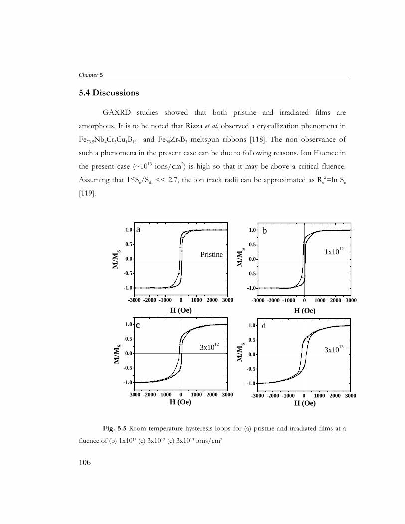
Figure 5.5 shows the hysteresis loop for pristine and irradiated films measured
with the applied field parallel to the film plane. It can be noticed that the coercivity for
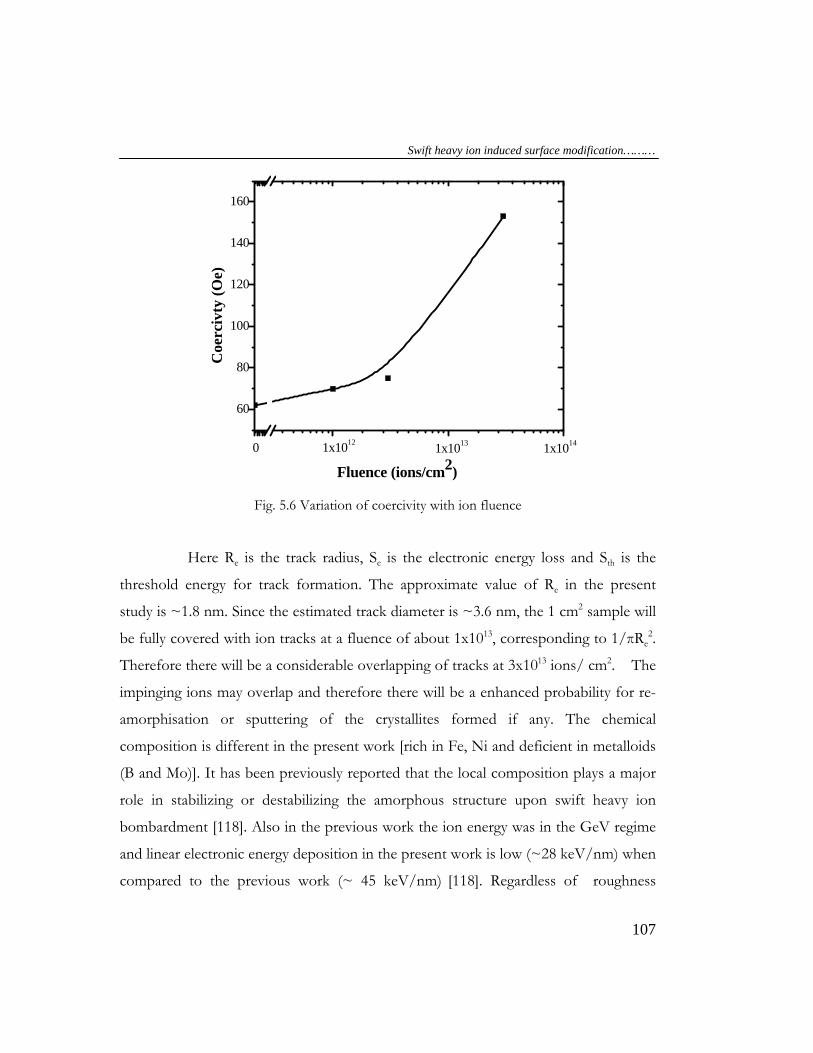
pristine and irradiated films are different. The variation of coercivity with fluence is
plotted and is depicted in figure 5.6. The squareness ratio (Mr/Ms) for pristine and
samples irradiated with swift heavy ions at various fluences of 1x10¹², 3x10¹² and
3x10¹³ ion/cm2 are 0.75, 0.67, 0.50 and 0.44 respectively. It is clear that the squareness
decreases with increase in the ion fluence.
Chapter 5
106
5.4 Discussions
GAXRD studies showed that both pristine and irradiated films are
amorphous. It is to be noted that Rizza et al. observed a crystallization phenomena in
Fe73.5Nb4Cr5Cu1B16 and Fe90Zr7B3 meltspun ribbons [118]. The non observance of
such a phenomena in the present case can be due to following reasons. Ion Fluence in
the present case (~1013 ions/cm2) is high so that it may be above a critical fluence.
Assuming that 1≤Se/Sth << 2.7, the ion track radii can be approximated as Re2=ln Se
[119].
-3000 -2000 -1000 0 1000 2000 3000
-1.0
-0.5
0.0
0.5
1.0
-3000 -2000 -1000 0 1000 2000 3000
-1.0
-0.5
0.0
0.5
1.0
-3000 -2000 -1000 0 1000 2000 3000
-1.0
-0.5
0.0
0.5
1.0
-3000 -2000 -1000 0 1000 2000 3000
-1.0
-0.5
0.0
0.5
1.0
M/M
S
H (Oe)
Pristine
a
M/M
S
H (Oe)
1x10¹²
b
M/M
s
H (Oe)
3x10¹²
c
M/M
S
H (Oe)
3x10¹³
d
Fig. 5.5 Room temperature hysteresis loops for (a) pristine and irradiated films at a
fluence of (b) 1x10¹² (c) 3x10¹² (c) 3x10¹³ ions/cm2
Swift heavy ion induced surface modification………
107
60
80
100
120
140
160C
oerc
ivty
(Oe)
Fluence (ions/cm2)
0 1x10¹² 1x10¹³ 1x10¹⁴
Fig. 5.6 Variation of coercivity with ion fluence
Here Re is the track radius, Se is the electronic energy loss and Sth is the
threshold energy for track formation. The approximate value of Re in the present
study is ~1.8 nm. Since the estimated track diameter is ~3.6 nm, the 1 cm2 sample will
be fully covered with ion tracks at a fluence of about 1x10¹³, corresponding to 1/πRe2.
Therefore there will be a considerable overlapping of tracks at 3x10¹³ ions/ cm2. The
impinging ions may overlap and therefore there will be a enhanced probability for re-
amorphisation or sputtering of the crystallites formed if any. The chemical
composition is different in the present work [rich in Fe, Ni and deficient in metalloids
(B and Mo)]. It has been previously reported that the local composition plays a major
role in stabilizing or destabilizing the amorphous structure upon swift heavy ion
bombardment [118]. Also in the previous work the ion energy was in the GeV regime
and linear electronic energy deposition in the present work is low (~28 keV/nm) when
compared to the previous work (~ 45 keV/nm) [118]. Regardless of roughness
Chapter 5
108
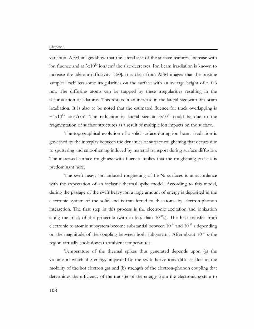
variation, AFM images show that the lateral size of the surface features increase with
ion fluence and at 3x10¹³ ion/cm2 the size decreases. Ion beam irradiation is known to
increase the adatom diffusivity [120]. It is clear from AFM images that the pristine
samples itself has some irregularities on the surface with an average height of ~ 0.6
nm. The diffusing atoms can be trapped by these irregularities resulting in the
accumulation of adatoms. This results in an increase in the lateral size with ion beam
irradiation. It is also to be noted that the estimated fluence for track overlapping is
~1x10¹³ ions/cm2. The reduction in lateral size at 3x10¹³ could be due to the
fragmentation of surface structures as a result of multiple ion impacts on the surface.
The topographical evolution of a solid surface during ion beam irradiation is
governed by the interplay between the dynamics of surface roughening that occurs due
to sputtering and smoothening induced by material transport during surface diffusion.
The increased surface roughness with fluence implies that the roughening process is
predominant here.
The swift heavy ion induced roughening of Fe-Ni surfaces is in accordance
with the expectation of an inelastic thermal spike model. According to this model,
during the passage of the swift heavy ion a large amount of energy is deposited in the
electronic system of the solid and is transferred to the atoms by electron-phonon
interaction. The first step in this process is the electronic excitation and ionization
along the track of the projectile (with in less than 10-16s). The heat transfer from
electronic to atomic subsystem become substantial between 10-14 and 10-12 s depending
on the magnitude of the coupling between both subsystems. After about 10-10 s the
region virtually cools down to ambient temperatures.
Temperature of the thermal spikes thus generated depends upon (a) the
volume in which the energy imparted by the swift heavy ions diffuses due to the
mobility of the hot electron gas and (b) strength of the electron-phonon coupling that
determines the efficiency of the transfer of the energy from the electronic system to
Swift heavy ion induced surface modification………
109
the lattice. Depending on the amount of energy transferred to the atomic system and
the attained temperature, specific phase changes can be induced such as transitions
from the solid to liquid phase or liquid to vapour phase. Surface roughening is
assumed to be because of the evaporation of atoms from a hot surface heated by an
inelastic thermal spike. This gives credence to the hypothesis that swift heavy ion
induced sputtering plays a predominant role in the surface roughening process of Fe-
Ni thin films.
Similar increase in surface roughness with an increase in ion fluence was also
observed by Mieskes et al [117] in Gold, Zirconium and Titanium metals. In their work
Au, Zr and Ti metals irradiated with 230 MeV Au ions exhibited an increase in surface
roughness with ion fluence. In the case of Ti the rms roughness increased from 100
nm to 1 mµ range when the ion fluence was increased from 2x10¹⁴ to 1x10¹⁵
ions/cm2. The increased surface roughness was attributed to the SHI induced
sputtering and the combined electronic and nuclear heating effect contributed to the
sputtering yield and was explained using an extended thermal spike model.
The observed coercivity changes can be correlated with the surface
evolution of the films with SHI irradiation. It is known that surface topography only
affects the magnetic properties of the surface region within 10-20 nm depth [121].
Hence surface techniques such as MOKE (Magneto Optic Kerr Effect) bring about a
better correlation between the surface morphology and magnetic properties because of
their surface sensitiviy [122]. However it is to be noted that the thickness of the films
in the present study is ~ 35 nm and though VSM is a bulk technique, the hysteresis
loop traced by the VSM represent the surface effects due to the limited thickness of
the film. The coercive force is a measure of the magnetic field necessary to reduce the
net magnetization of a ferromagnetic material from its saturation value in some
selected direction to zero in that direction. The coercivity depends on the way in
which the magnetization changes. There are two mechanisms by which this occurs a)
Chapter 5
110
by net magnetization rotation 2) by domain wall motion. In soft magnetic materials
the change in magnetization is primarily due to domain wall motion. Since this is a low
energy process when compared to rotation of the net magnetization, the domain wall
motion is associated with small coercive fields. Also it should be noted that pinning
centers such as dislocations and grain boundaries are non existent in an amorphous
alloy. So the possible mechanism for the increase in coercivity is the presence of
surface pinning states. In the present case the changes in coercivity are entirely due to
the modifications on the surface of the film and no other mechanisms (for example
nano crystallization by heating effects of ion beams) are contributing to it. Very small
irregularities on the surface of a film inhibit the passage of a domain wall because the
energy stored within a domain wall surrounding such a region is smaller than in an
undisturbed domain wall and consequently the system energy must be increased to
enable the domain wall motion. A possible mechanism involved in this surface pinning
can be as follows. When the magnetization within a domain wall intersects the surface,
the magnetostatic energy is greater for surface regions which are normal to the domain
wall than for those which are not. Consequently, the wall prefers irregular surface
regions and may be pinned at such locations [123].
From AFM images and data it is clear that the surface roughness increases with
increase in ion fluence and therefore more sites will be available for domain wall
pinning and this resulted in an increased coercivity at higher ion fluences [see figure
5.7]. The increase in the value of coercivity with an increase in surface roughness is in
line with the observations of other researchers [124-126]. Li et al. [124] studied the
magnetization reversal process of Co film deposited on plasma etched Si substrates.
The increased coercivity was attributed to the contribution of domain wall pinning in
the magnetization reversal mechanism. Doherty et al. [125] observed an increase in
coercivity with increased surface roughness in magnetic multilayer systems. They
explained that roughness caused a discontinuity in the magnetization at the surface,
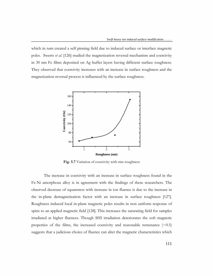
Swift heavy ion induced surface modification………
111
which in turn created a self pinning field due to induced surface or interface magnetic
poles. Swerts et al. [126] studied the magnetization reversal mechanism and coercivity
in 30 nm Fe films deposited on Ag buffer layers having different surface roughness.
They observed that coercivity increases with an increase in surface roughness and the
magnetization reversal process is influenced by the surface roughness.
1 2 3
60
80
100
120
140
160
Coe
rciv
ity (O
e)
Roughness (nm) Fig. 5.7 Variation of coercivity with rms roughness
The increase in coercivity with an increase in surface roughness found in the
Fe-Ni amorphous alloy is in agreement with the findings of these researchers. The
observed decrease of squareness with increase in ion fluence is due to the increase in
the in-plane demagnetization factor with an increase in surface roughness [127].
Roughness induced local in-plane magnetic poles results in non uniform response of
spins to an applied magnetic field [128]. This increases the saturating field for samples
irradiated at higher fluences. Though SHI irradiation deteriorates the soft magnetic
properties of the films, the increased coercivity and reasonable remenance (~0.5)
suggests that a judicious choice of fluence can alter the magnetic characteristics which
Chapter 5
112
suits novel applications of magnetic thin films. For example, there is intense interest,
for data storage applications, in patterned magnetic media; in such media magnetic
“contrast” is required at periodic intervals. This contrast can be obtained by alternate
soft and hard magnetic regions by subjecting selected areas to SHI irradiation. The
present study demonstrates that swift heavy ion is an effective tool in modifying the
surface morphology of a magnetic thin film. This property can be used for controlling
useful magnetic properties like coercivity.
5.5 Conclusions
In conclusion, it was found that bombardment of 108 MeV Ag8+ ions can
result in roughening of Fe-Ni based amorphous thin film surfaces. The ion irradiation
induced roughening can be due to the sputtering phenomena exhibited as a result of
high electronic energy deposition. The coercivity of these films was found to increase
with an increase in ion fluence. The increased coercivity is due to the increased surface
roughness which provides pinning sites for inhibiting domain wall motion. These
results are promising and can be useful in tailoring the magnetic properties of a
magnetic material in a controlled fashion.