ex-situ electron microscopy study of solid electrolyte
TRANSCRIPT

Ex-Situ Electron Microscopy Study of Solid Electrolyte Interphase Formed byCharge-Discharge Reaction of Silicon Negative Electrode in Lithium-Ion SecondaryBattery+1
Yutaka Shimauchi1,2, Sachi Ikemoto1, Shigekazu Ohmori1 and Takaomi Itoi2,+2
1JFE Techno-Research Corporation, Chiba 260-0835, Japan2Department of Mechanical Engineering, Chiba University, Chiba 263-8522, Japan
A SEI (Solid Electrolyte Interphase) is formed on the surface layer of the negative electrode active material of a lithium ion secondarybattery (LIB) during the initial charging process, and its morphology and structure significantly affect performance and safety. In this study, byconducting ex situ experiments, SEM, TEM and STEM-EELS observations were performed on Si negative electrodes under charge state withinan actual battery and Si negative electrodes directly charged on a TEM thin film, revealed morphology and structure of the SEI. All of theprocesses from specimen preparation for electron microscopy observation to specimen transport were performed under non-atmosphericexposure conditions.
The SEI on the surface of the Si negative electrode grew thicker as the charge depth increased. On the other hands, LixSi amorphous phasedue to the lithiation by solid-state reaction was confirmed inside the Si negative electrode. It was found that Li2O was formed on the most surfaceof the Si negative electrode at the initial stage of charging, and the SEI was mainly composed of Li2O. The SEI of about 1 µm was observed onthe Si negative electrode after 40% charge, and the thickness of the SEI decreased to less than 1/5 after discharge.[doi:10.2320/matertrans.MT-M2021070]
(Received April 21, 2021; Accepted May 10, 2021; Published June 11, 2021)
Keywords: solid electrolyte interphase, Si negative electrode, microstructure, ex-situ TEM, non-atmospheric exposure
1. Introduction
Since lithium ion secondary batteries play a central roleas energy storage devices, material development orientedtoward high capacities is desirable.1) To achieve this goal,attention has been focused on Si, which is expected to realizean increase of approximately 10 times in the capacity-to-weight ratio in comparison with carbon materials in negativeelectrodes capable of storing larger quantities of Li.2) Instudies of electrochemical lithiation, anisotropy of the Liintrusion direction in Si crystals via the charging reactionhas been reported based on first-principles calculations aswell as other simulation techniques, in situ transmissionelectron microscopy (TEM) imaging and ex-situ observationsunder non-atmospheric exposure conditions.38) In a lithiumion battery (LIB), a passivation layer known as solidelectrolyte interphase (SEI) is formed at the interface betweenthe negative electrode and electrolyte during the initialcharging process. It is known that the morphology andstructure of the SEI significantly affect the performance andsafety of the battery.9,10) The SEI formation mechanism andits structural properties have also been investigated via first-principles calculations,11,12) and it has been reported that theSEI consists of multiple inorganic and organic compounds,including Li oxides, fluorides, and carbonates.13) AlthoughSEI formation during the initial charging process initiates dueto the reductive decomposition products of the electrolyte,mainly at the surface of the negative electrode activematerial, and proceeds via electron transfer, this reaction iscomplex, and the composition and structure of the SEI arethought to change depending on the type of electrode
material, type of electrolyte, ambient temperature, andcharging conditions. Various models have been proposedbased on first-principles calculations. These include a modelin which the reductive decomposition products of theelectrolyte accumulate directly on the negative electrodesurface and a model in which these products do notaccumulate immediately on the negative electrode surfacebut form aggregates by reacting in the electrolyte at a slightdistance from the negative electrode and then accumulateon the surface of the negative electrode.14) Therefore,identification of the component substances of the SEI andclarification of their formation position and morphologythrough experimental techniques will provide crucial knowl-edge for modeling the SEI formation mechanism throughcomputational science. Considering the nanometer size ofthe SEI in the initial charging process, TEM is the ideal toolto perform SEI observations. However, there are only fewexamples of direct observation and discussion of SEIformation on a Si negative electrode during charge/dischargeprocesses using an actual battery structure. Techniques forobserving the negative electrode in the charged state arelimited because the charged electrode contains Li, which isextremely active when exposed to moisture and air. Forexample, Nie et al. reported the results of observations of themicrostructural change after charging when graphite particleswere dispersed on the TEM specimen stage under non-atmospheric exposure conditions.15) The authors constructeda simple lithium ion cell by surrounding the TEM stagewith dispersed graphite with an ordinary graphite negativeelectrode, and they were thus able to observe the cell aftercharging. However, due to the difference in the electricalresistance of the TEM stage and the surrounding negativeelectrode as well as other possible factors, it is necessary todetermine whether a uniform charging reaction can actuallytake place in these conditions. As this suggests, operand
+1This Paper was Originally Published in Japanese in Japan Inst. Met.Mater. 84 (2020) 382390.
+2Corresponding author, E-mail: [email protected]
Materials Transactions, Vol. 62, No. 8 (2021) pp. 1079 to 1088©2021 The Japan Institute of Metals and Materials

experiments aimed at examining the microstructural changesin a negative electrode during charge/discharge processes arefrequently problematic due to the difficulty of handling thenegative electrode in the charged state.
In this work, we fabricated an actual battery using Si, whichis a promising high capacity material for use as the negativeelectrode active material of lithium ion secondary batteries.Furthermore, we carried out microstructural observations ofthe SEI formation process caused by the charge/dischargereaction and the changes in the internal microstructure ofthe Si negative electrode using electron microscopy. Speci-mens for TEM observation were prepared via the focused ionbeam (FIB) technique in order to appropriately evaluate theobservation position, and the SEI after charging anddischarging was compared and discussed. When attemptingto observe the SEI formed on the surface layer of the negativeelectrode active material during charging, damage caused bythe ion beam in the FIB method is a concern. Therefore, weprepared an actual battery that could be charged directly ona TEM thin film (Si negative electrode) which was thinlysliced via ion milling. TEM observations of these Si negativeelectrodes were then carried out after inducing a uniformcharging reaction in the entire specimen. In the observationand analysis of the charge/discharge states of the battery,ex-situ experiments were conducted under strict environ-mental control to prevent contact with atmosphere in allprocesses, from disassembly of the battery to preparation andtransport of the electron microscopy specimens.
2. Experimental Methods
2.1 Preparation of the lithium ion secondary cellThe negative electrodes were prepared by coating a metal
foil collector (Cu foil) having a thickness of 20 µm with Sisingle crystal powder:acetylene black:polyvinylidene fluo-ride = 80:10:10mass% as the negative electrode material.They were then dried and pressed. Acetylene black was usedto reduce the electrical resistance of the electrode. Theaverage particle size of the Si single crystal powder was10 µm, and the coating density of the electrode was 2.1mg/cm2 per unit surface area. Since only the negativeelectrode was evaluated in this experiment, a Li metal foilwas used in the counter electrode (positive electrode) toeliminate the influence of the positive electrode activematerial, and the secondary cell structure was created usinga polyethylene separator with a thickness of 20 µm. Figure 1shows the photograph of the prepared battery. The electrodeswere punched to a diameter (¤) of 16mm and were used to
construct coin batteries. The electrolytic solution was amixture of 1mol/L of LiPF6 in a solvent consisting ofethylene carbonate and diethyl carbonate with a volume ratioof 1:1.
2.2 Charging/discharging and disassembly of the lithi-um ion secondary cell
The insertion and desorption states of Li in the Si particleswere observed and analyzed at various states of charge(SOCs). The SOC was adjusted through the charge/dischargedevice assuming 4.2Ah/g as the theoretical capacity (upperlimit in the fully charged state) of Si. A CompactStat(Ivium Technologies) electrochemical interface was used forcharging/discharging. For scanning electron microscopy(SEM) observations of possible differences in the chargedstate, batteries with SOCs of 40% and 100% were prepared.A battery which was fully discharged (SOC = 0%) afterbeing charged to a SOC of 40% was also prepared. Aftercharging, the coin batteries were disassembled in a gloveboxin which the air had been replaced to a sufficiently low levelwith high purity Ar gas. The environment in the gloveboxwas maintained at a dewpoint of ¹80°C or less and at anoxygen concentration of 1 ppm or less. The coin batterieswere disassembled in the glovebox immediately aftercharging or discharging. The samples for analysis wereprepared by taking only the separated negative electrode,thoroughly cleaning the electrolyte with pure dimethylcarbonate, and drying.
2.3 SEM observationsAfter disassembly in the glovebox, the cross section of
the cleaned negative electrodes was observed via FESEM(S-4800, Hitachi High-Tech Corporation). The specimens forcross-sectional observations were prepared using an ionmilling system (IM4000, Hitachi High-Tech), and a dedicatedtransfer vessel was used to transfer the specimens from theglovebox to the ion milling system. This transfer vessel hasan airtight structure which can maintain an inert atmosphereor vacuum around a specimen and makes it possible totransfer specimens between devices consistently withoutexposure to atmosphere. The same type of vessel was alsoused to transfer the milled specimens to the SEM setupwithout exposure to atmosphere. Since the reaction of thecharged negative electrode with air is particularly remarkableand degradation of the specimens with time is a concern,the sequence of processes from disassembly to SEMobservations was performed quickly and continuously. Anaccelerating voltage of 4.0 kV and a beam current of 0.2mAwere used for ion milling.
2.4 TEM and STEM observations and EELS analysisThe cross sections of the Si particles in the negative
electrodes charged to a SOC of 40% and discharged from aSOC of 40%, which were observed via SEM in section 2.3,were also observed via TEM and STEM (ARM200F, JEOL)at an accelerated voltage of 200 kV. Furthermore, EELS(Enfinium, GATAN, Inc.) analysis was conducted. Thespecimens for TEM observations were prepared in the samemanner as those for SEM observations; that is, the cellswere disassembled in a glovebox, and the cleaned and dried
10mm
Fig. 1 Image of the coin-type battery.
Y. Shimauchi, S. Ikemoto, S. Ohmori and T. Itoi1080
negative electrodes were transferred to the FIB (VERSA 3D,FEI) using an FIB transfer vessel. Regarding the thin filmpreparation conditions for the FIB, the accelerating voltageand beam current were set to 30 kV and 30 nA, respectively,up to a film thickness of 500 nm. The beam diameter wasnarrowed by reducing the beam current in stages, and, for athickness below 200 nm, the FIB process was carried out withthe accelerating voltage and beam current reduced to 10 kVand several pA, respectively. Since it was not possible totransfer the specimens directly from the FIB device to theTEM while retaining non-atmospheric exposure conditions,the specimens from the FIB system were returned once tothe glovebox, where they were then transferred to a differentnon-atmospheric exposure transfer vessel.
2.5 Preparation of dedicated negative electrodes forTEM observations, charging, and TEM observa-tions
Considering the possibility of degradation of the SEIcaused by FIB during the preparation of the thin filmspecimens for TEM observations, the Si negative electrodeswere charged after the thin film preparation, and the SEI wasimaged. Here, a proportion of the electrode film (Si negativeelectrode film) prepared as described in section 2.1 waspunched to a diameter of 3mm, and the thin films wereprepared using an Ar ion milling device (Dual Ion Mill 600,GATAN) under liquid nitrogen cooling. An incident angleof 12°, a specimen rotation speed of 5 rpm, an acceleratingvoltage of 4.0 kV, and a beam current of 0.4mAwere used forAr ion milling. Firstly, the Si negative electrode thin filmswere observed via TEM before charging. The thin filmspecimens were then charged, and TEM was used to imagethe same location as before charging in order to investigatethe SEI formed after charging. Figure 2(a) shows an imageof a HS (Hohsen) flat cell, and Fig. 2(b) shows a schematicdiagram of the structure inside the HS flat cell used forcharging. As for the experiment described in section 2.1, aLi metal foil was used in the counter electrode (positiveelectrode), and a half-cell structure using a polypropylene
separator with a thickness of 20 µm was constructed as thecell structure. The electrolytic solution used here wasprepared by mixing 1mol/L of LiPF6 in a solvent consistingof ethylene carbonate and diethyl carbonate with a volumeratio of 1:1, and the cell was charged using the above-mentioned CompactStat (Ivium Technologies). The thin filmprepared for TEM observations was weighed, and the SOCwith respect to the theoretical capacity was calculated basedon the blending ratio of the electrode film. TEM observationswere conducted after charging to a SOC of 20%. In thisexperiment, charging was limited to a SOC of 20% becauseof the concern that it would not be possible to maintain thethin film state due to the swelling of the Si particles causedby charging. After disassembling the battery, the specimenwas transferred to the TEM setup via the glovebox so asto prevent exposure to atmosphere, in the same manner asdescribed in section 2.4.
3. Results and Discussion
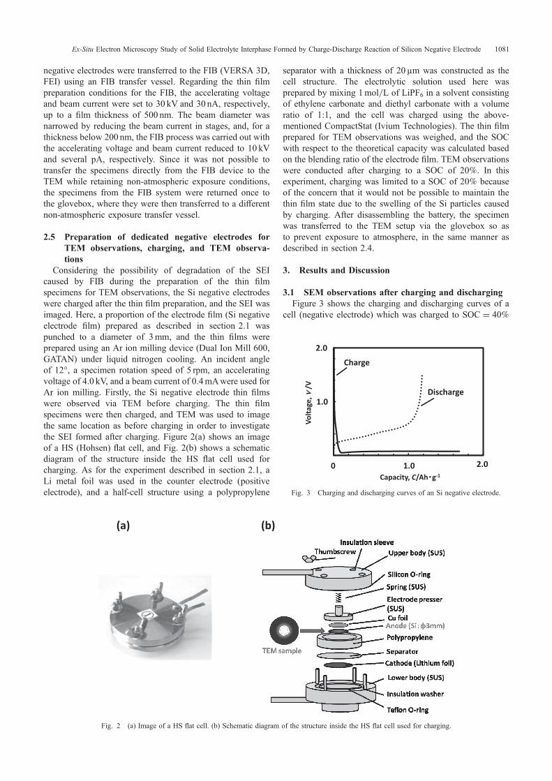
3.1 SEM observations after charging and dischargingFigure 3 shows the charging and discharging curves of a
cell (negative electrode) which was charged to SOC = 40%
(a) (b)
Fig. 2 (a) Image of a HS flat cell. (b) Schematic diagram of the structure inside the HS flat cell used for charging.
Volt
age,
/V
2.0
1.0
0 1.0 2.0Capacity, C/Ah g-1
Charge
Discharge
Fig. 3 Charging and discharging curves of an Si negative electrode.
Ex-Situ Electron Microscopy Study of Solid Electrolyte Interphase Formed by Charge-Discharge Reaction of Silicon Negative Electrode 1081
and then discharged. Since the charging and discharging rateswere set to a C-rate equivalent to 0.1C, the charging anddischarging times for SOC = 40% were approximately 4 h.From this figure, it can be seen that the voltage decreased dueto charging from around 2.8V, which was the open circuitvoltage (OVC) before charging. Furthermore, upon discharg-ing after charging to SOC = 40%, which is equivalent toapproximately 1.7Ah/g, only about 1.2Ah/g was dis-charged. It is believed that this occurs due to the fact thatthe Li ions transferred into the Si negative electrode remain inthe electrode, resulting in an irreversible loss of capacity.
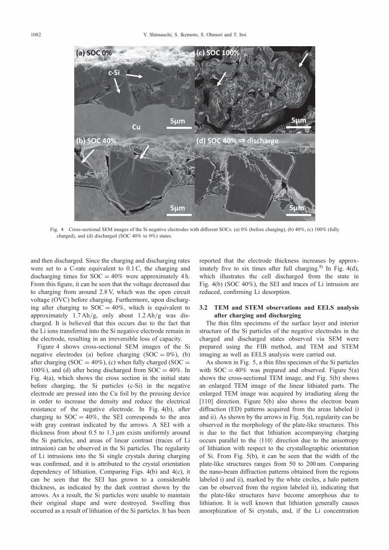
Figure 4 shows cross-sectional SEM images of the Sinegative electrodes (a) before charging (SOC = 0%), (b)after charging (SOC = 40%), (c) when fully charged (SOC =100%), and (d) after being discharged from SOC = 40%. InFig. 4(a), which shows the cross section in the initial statebefore charging, the Si particles (c-Si) in the negativeelectrode are pressed into the Cu foil by the pressing devicein order to increase the density and reduce the electricalresistance of the negative electrode. In Fig. 4(b), aftercharging to SOC = 40%, the SEI corresponds to the areawith gray contrast indicated by the arrows. A SEI with athickness from about 0.5 to 1.3 µm exists uniformly aroundthe Si particles, and areas of linear contrast (traces of Liintrusion) can be observed in the Si particles. The regularityof Li intrusions into the Si single crystals during chargingwas confirmed, and it is attributed to the crystal orientationdependency of lithiation. Comparing Figs. 4(b) and 4(c), itcan be seen that the SEI has grown to a considerablethickness, as indicated by the dark contrast shown by thearrows. As a result, the Si particles were unable to maintaintheir original shape and were destroyed. Swelling thusoccurred as a result of lithiation of the Si particles. It has been
reported that the electrode thickness increases by approx-imately five to six times after full charging.8) In Fig. 4(d),which illustrates the cell discharged from the state inFig. 4(b) (SOC 40%), the SEI and traces of Li intrusion arereduced, confirming Li desorption.
3.2 TEM and STEM observations and EELS analysisafter charging and discharging
The thin film specimens of the surface layer and interiorstructure of the Si particles of the negative electrodes in thecharged and discharged states observed via SEM wereprepared using the FIB method, and TEM and STEMimaging as well as EELS analysis were carried out.
As shown in Fig. 5, a thin film specimen of the Si particleswith SOC = 40% was prepared and observed. Figure 5(a)shows the cross-sectional TEM image, and Fig. 5(b) showsan enlarged TEM image of the linear lithiated parts. Theenlarged TEM image was acquired by irradiating along the[110] direction. Figure 5(b) also shows the electron beamdiffraction (ED) patterns acquired from the areas labeled i)and ii). As shown by the arrows in Fig. 5(a), regularity can beobserved in the morphology of the plate-like structures. Thisis due to the fact that lithiation accompanying chargingoccurs parallel to the ©110ª direction due to the anisotropyof lithiation with respect to the crystallographic orientationof Si. From Fig. 5(b), it can be seen that the width of theplate-like structures ranges from 50 to 200 nm. Comparingthe nano-beam diffraction patterns obtained from the regionslabeled i) and ii), marked by the white circles, a halo patterncan be observed from the region labeled ii), indicating thatthe plate-like structures have become amorphous due tolithiation. It is well known that lithiation generally causesamorphization of Si crystals, and, if the Li concentration
(b) SOC 40%
(a) SOC 0%
c-Si
(c) SOC 100%
(d) SOC 40% discharge
5μm
Cu
5μm
5μm5μm
Fig. 4 Cross-sectional SEM images of the Si negative electrodes with different SOCs. (a) 0% (before charging), (b) 40%, (c) 100% (fullycharged), and (d) discharged (SOC 40% to 0%) states.
Y. Shimauchi, S. Ikemoto, S. Ohmori and T. Itoi1082
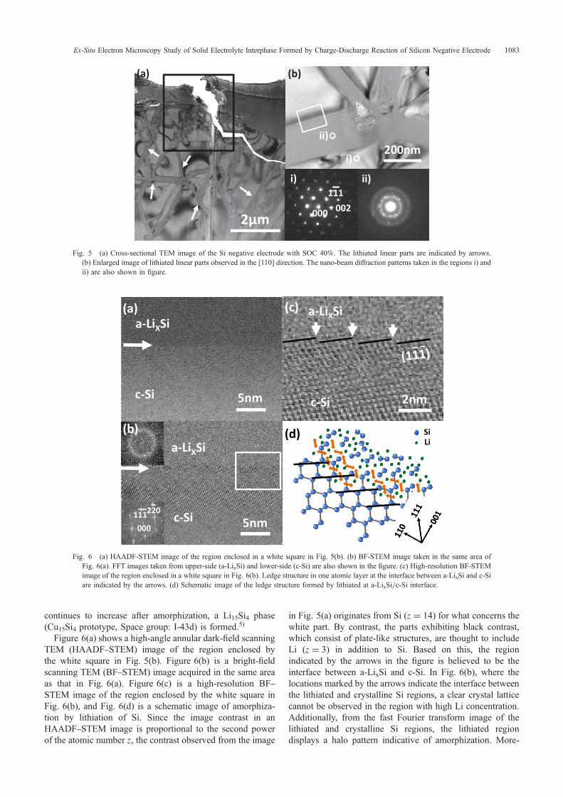
continues to increase after amorphization, a Li15Si4 phase(Cu15Si4 prototype, Space group: I-43d) is formed.5)
Figure 6(a) shows a high-angle annular dark-field scanningTEM (HAADFSTEM) image of the region enclosed bythe white square in Fig. 5(b). Figure 6(b) is a bright-fieldscanning TEM (BFSTEM) image acquired in the same areaas that in Fig. 6(a). Figure 6(c) is a high-resolution BFSTEM image of the region enclosed by the white square inFig. 6(b), and Fig. 6(d) is a schematic image of amorphiza-tion by lithiation of Si. Since the image contrast in anHAADFSTEM image is proportional to the second powerof the atomic number z, the contrast observed from the image
in Fig. 5(a) originates from Si (z = 14) for what concerns thewhite part. By contrast, the parts exhibiting black contrast,which consist of plate-like structures, are thought to includeLi (z = 3) in addition to Si. Based on this, the regionindicated by the arrows in the figure is believed to be theinterface between a-LixSi and c-Si. In Fig. 6(b), where thelocations marked by the arrows indicate the interface betweenthe lithiated and crystalline Si regions, a clear crystal latticecannot be observed in the region with high Li concentration.Additionally, from the fast Fourier transform image of thelithiated and crystalline Si regions, the lithiated regiondisplays a halo pattern indicative of amorphization. More-
2μm
200nm
ii)
(a) (b)
i)
i)
ii)
002
111
000
Fig. 5 (a) Cross-sectional TEM image of the Si negative electrode with SOC 40%. The lithiated linear parts are indicated by arrows.(b) Enlarged image of lithiated linear parts observed in the [110] direction. The nano-beam diffraction patterns taken in the regions i) andii) are also shown in figure.
5nm
5nm
(a)
2nm
(c)
(d)
220111
c-Si
a-LiXSi
(b)
a-LiXSi
c-Si
a-LiXSi
c-Si
SiLi
000
Fig. 6 (a) HAADF-STEM image of the region enclosed in a white square in Fig. 5(b). (b) BF-STEM image taken in the same area ofFig. 6(a). FFT images taken from upper-side (a-LixSi) and lower-side (c-Si) are also shown in the figure. (c) High-resolution BF-STEMimage of the region enclosed in a white square in Fig. 6(b). Ledge structure in one atomic layer at the interface between a-LixSi and c-Siare indicated by the arrows. (d) Schematic image of the ledge structure formed by lithiated at a-LixSi/c-Si interface.
Ex-Situ Electron Microscopy Study of Solid Electrolyte Interphase Formed by Charge-Discharge Reaction of Silicon Negative Electrode 1083

over, from Fig. 6(c), it can be seen that the ð1�1�1Þ directionforms a step (ledge) structure in one atomic layer at theinterface between a-LixSi and c-Si, as indicated by thearrows.
Liu et al. investigated the formation of the a-LixSi phaseby lithiation in Si nanowires via in situ TEM imaging ofthe lithiation process during the charging reaction. Theyreported that Si becomes amorphous due to lithiation, whichcauses separation (fracture) in one atomic layer through themovement of the ledge structure via a solid state reaction atthe amorphous/crystalline interface.16) In the present work, itis speculated that amorphization proceeds via movement ofthe interface through a solid state reaction originating fromthe edge of the {111} facet (crystal wall) marked by thearrows in Fig. 6(c). Molecular dynamic calculations wereused to investigate electrochemical lithiation, and the processwhereby interfacial movement occurs due to delaminationof the {111} facets and subsequent amorphization when Liintrudes between adjoining {111} plane layers was clarifiedat the atomic level.17) Since the surface energy of the {111}planes of Si is lower than that of other crystal planes,cleavage of the {111} planes occurs more easily. Therefore,as shown in the schematic diagram in Fig. 6(d), it is thoughtthat interfacial movement occurs through a process in whichLi atoms occupy the tetrahedral sites of Si crystals. Thus, asthe concentration of Li increases, amorphization proceeds via
destruction of the Si crystal structure as the Si bonds betweenthe {111} planes are broken. This process appears as a zigzagpattern, as indicated by the arrows in Fig. 6(d). As the chargedepth increases and the Li concentration in the Si crystalsincreases, an amorphous phase is formed through thedestruction of the crystal lattice accompanying the increasedlithiation at tetrahedral sites, and this region expands throughpreferential growth in the ©110ª direction.8) The anisotropyof the linear regions with size of several microns shown inthe SEM image in Fig. 4 and in the TEM image in Fig. 5are likely to originate from this anisotropic growth of theamorphous phase. Amorphization caused by the solid statereaction originated during lithiation has also been confirmedby observation of the ledge structure in an ex-situ experimentusing the negative electrode of an actual battery structure.This is consistent with the abovementioned in situ TEMimaging results for the lithiation of the Si nanowires obtainedby Liu et al. Thus, the present work also demonstrates theeffectiveness of experiments under non-atmospheric exposureconditions for the observation of the microstructure of Sinegative electrodes.
Figure 7(a) shows the cross-sectional HAADFSTEMimage of the near-surface area of the Si particles in thenegative electrode with SOC = 40%, including the SEI, inthe region enclosed by the black square in Fig. 5(a).Figure 7(b) displays the enlarged HAADFSTEM image of
1μm
500nm
(a)
(b)
(c)
EELS map area
Red:Li-K (56.8-66.5 eV) Blue Si-L (98.6-108.3 eV)
100nm
i)
(d)
SEI
Inte
nsity
(arb
.uni
ts)
Energy loss (eV)Fig. 7 (a) Cross-sectional HAADF-STEM image of the Si negative electrode with SOC 40% enclosed in a black square in Fig. 5(a).
(b) Enlarged image enclosed in a white square in Fig. 7(a). (c) Enlarged STEM-EELS map (red: Li, blue: Si) enclosed in a broken line inFig. 7(b). (d) The EEL spectra obtained in an area i) in Fig. 7(c) and Li2O standard sample.
Y. Shimauchi, S. Ikemoto, S. Ohmori and T. Itoi1084
the region enclosed by the white square in Fig. 7(a).Figure 7(c) illustrated the EELS map of the region enclosedby the white dashed line in Fig. 7(b), where red indicatesLi and blue indicates Si. Figure 7(d) shows the EEL spectraobtained for the area labeled i) in Fig. 7(c). In Fig. 7(a), ablack contrast is observed in the linear parts shown inFig. 5(a), and the existence of a region with a high Liconcentration can be confirmed. From the enlarged imagein Fig. 7(b), it can be seen that a SEI with a thickness ofapproximately 1 µm has formed, which is in excellentagreement with the results of the SEM observations inFig. 4(b). Moreover, it is clear that the SEI also containsstructures with size of several tens of nanometers anddifferent compositions, which are indicated by the whitecontrast.
According to Peled et al., the SEI formed on the surface ofa negative electrode as a consequence of the reaction betweenan electrolytic solution and Li is not a single oxide but israther thought to be composed of inorganic compounds, suchas LiF, Li2CO3, and Li2O, and organic compounds.13)
Therefore, an EELS area analysis (two-dimensional scan)was performed in the region enclosed by the dashed line,which includes the SEI that formed on the surface of the Siparticles. Figure 7(c) indicates that the main component ofthe SEI is Li. Furthermore, in the spectra obtained for the area
labeled i) in Fig. 7(c), a LiK absorption edge was observedaround 60 eV, and the absorption edge of the high energyside was larger than that of the low energy side. As thisapproximates the spectrum obtained from a Li2O standardsample, the main component of the SEI is considered to beLi2O. However, the structure described above was notidentified in detail, and Ga ions originating from the FIBprocess could also be present.
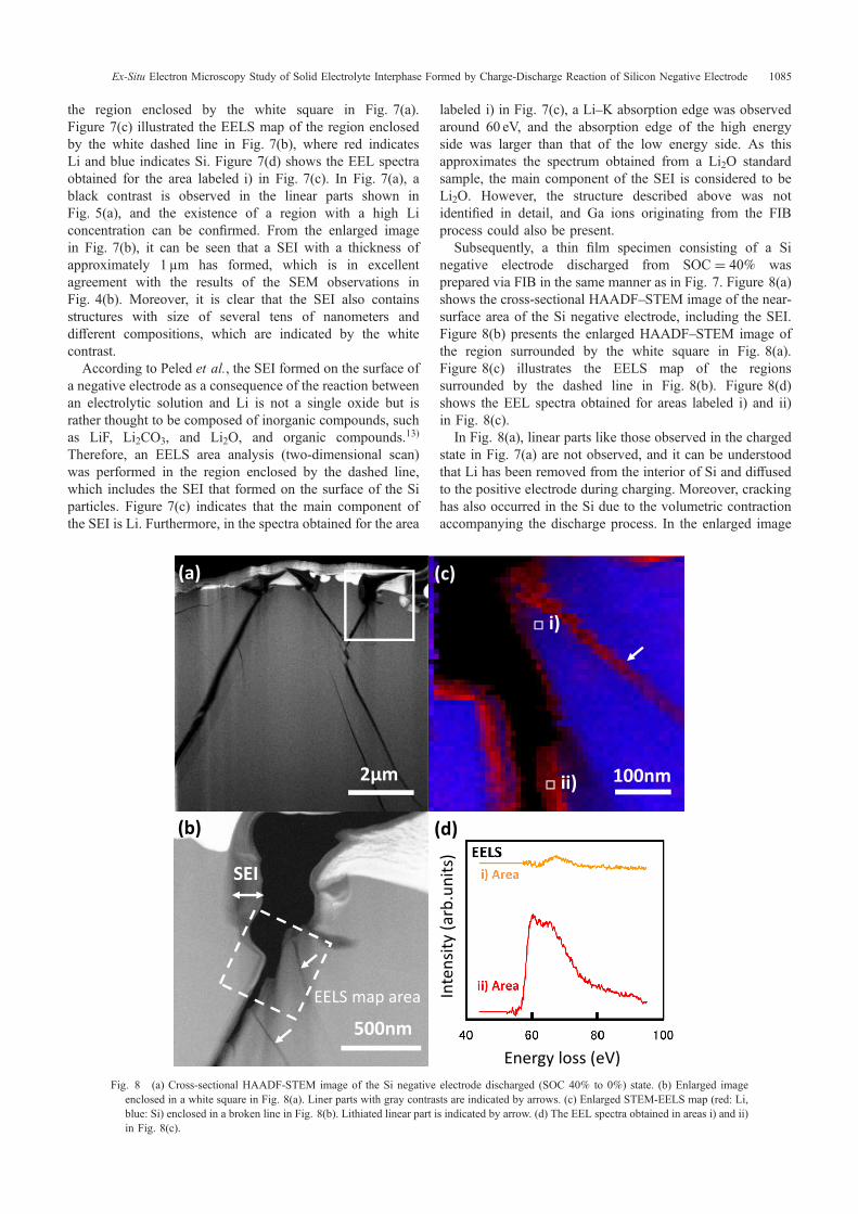
Subsequently, a thin film specimen consisting of a Sinegative electrode discharged from SOC = 40% wasprepared via FIB in the same manner as in Fig. 7. Figure 8(a)shows the cross-sectional HAADFSTEM image of the near-surface area of the Si negative electrode, including the SEI.Figure 8(b) presents the enlarged HAADFSTEM image ofthe region surrounded by the white square in Fig. 8(a).Figure 8(c) illustrates the EELS map of the regionssurrounded by the dashed line in Fig. 8(b). Figure 8(d)shows the EEL spectra obtained for areas labeled i) and ii)in Fig. 8(c).
In Fig. 8(a), linear parts like those observed in the chargedstate in Fig. 7(a) are not observed, and it can be understoodthat Li has been removed from the interior of Si and diffusedto the positive electrode during charging. Moreover, crackinghas also occurred in the Si due to the volumetric contractionaccompanying the discharge process. In the enlarged image
100nm
500nm
(a) (c)
EELS map area
2μm
(b)
i)
ii)
(d)
Inte
nsity
(arb
.uni
ts)
Energy loss (eV)
SEI
Fig. 8 (a) Cross-sectional HAADF-STEM image of the Si negative electrode discharged (SOC 40% to 0%) state. (b) Enlarged imageenclosed in a white square in Fig. 8(a). Liner parts with gray contrasts are indicated by arrows. (c) Enlarged STEM-EELS map (red: Li,blue: Si) enclosed in a broken line in Fig. 8(b). Lithiated linear part is indicated by arrow. (d) The EEL spectra obtained in areas i) and ii)in Fig. 8(c).
Ex-Situ Electron Microscopy Study of Solid Electrolyte Interphase Formed by Charge-Discharge Reaction of Silicon Negative Electrode 1085

in Fig. 8(b), the thickness of the SEI is about 200 nm and isthus decreased after discharge. Black contrast can beobserved at the Si negative electrode surface and at thepositions indicated by the arrows, and differences in thecomposition have also occurred in Si after discharge. As aresult of the EELS area analysis in the region enclosed bythe dashed line, which includes the SEI, Fig. 8(c) showsthat the SEI and the positions indicated by the arrows containLi. The EEL spectrum of the interior of the Si in the arealabeled i) in Fig. 8(c) shows that the interior of the Sicontains almost no Li; however, Li remains in the linear partsindicated by the arrows in the figure. The anisotropy of theLi diffusion path with respect to the crystal orientation ofSi during charging (Li intrusion) has already been noted.However, since linear parts with decreased widths incomparison with the charged state remained after discharge,it is thought that also Li follows the same paths duringdischarge and diffuses toward the positive electrode via theSEI. The slight amount of Li observed in the EEL spectrumof the area labeled i) is believed to originate from the a-LixSidetected in the thickness direction of the TEM thin film,because the area around the interface between the Si regionand the linear parts was investigated in the area analysis.Since the EEL spectrum obtained in the area labeled ii)approximates the spectrum shape of the Li2O standard sampleobserved in Fig. 7(d), it is thought that Li2O remained on thesurface of the Si particles of the negative electrode, and thethickness of the SEI decreased after discharge.
During the charge/discharge reactions, Li ions arerepeatedly inserted in and removed from the interior of thenegative electrode via a process of diffusion through the SEIand its interface with the negative electrode. Although theSEI is formed after initial charging and then undergoesrepeated adsorption/desorption as a result of charge/discharge processes, it is known that the SEI also remainson the surface of the negative electrode after discharge, andits thickness gradually increases upon increasing the numberof charge/discharge cycles.18) As a result of the observationand comparison of the microstructure of the Si negativeelectrode during charge/discharging processes, a plate-likemicrostructure consisting of a-LixSi formed via lithiation anda SEI with a thickness of approximately 1 µm were observedin the interior of the Si crystal and on the surface layer,respectively. Since Li2O forms in close proximity to the Sinegative electrode (i.e., immediately above the Si surface),it was assumed that Li2O is the primary component of theSEI. As confirmed via SEM and TEM observations, afterdischarge, the Li ions in Si are removed, the linear parts areextinguished, and the thickness of the SEI decreases to 1/5 orless than that in the charged state. The SEI has the function offacilitating the reaction with the negative electrode; however,since it also causes irreversible loss of capacity, which affectsthe life of the battery, it is important to identify its componentsubstances and clarify their formation sites and morphology.From Figs. 7(c) and 8(c), it can be seen that Li2O exists nearthe interface with the Si particles of the negative electrode.The properties of the SEI and its adhesion to the negativeelectrode are thought to depend strongly on its initialstructure.14) As a consequence, it was deemed appropriateto prepare TEM specimens via the FIB method in order to
properly evaluate the observation position. In a previousexperimental study on graphite negative electrodes, it wasreported that the inner-SEI near the negative electrodeinterface has a high content of Li2O and other inorganiccomponents,19) and the fact that a similar tendency existswith different negative electrode active materials is veryinteresting.
3.3 Charging of TEM thin films (Si negative electrodethin films) and TEM/STEM imaging and EELSanalysis before/after charging
When using FIB, the possibility of damaging the structureof the SEI is a concern because the thin film is prepared byhigh energy (30 kV) irradiation of Ga ions on the samplematerial. Therefore, in the present study, TEM observationsof the Si negative electrode before/after charging wereconducted using the method described in section 2.5 in orderto determine whether the SEI was damaged by FIB.
Figure 9 shows the charging curve of the TEM thin filmprepared via FIB when charged with the flat cell shown inFig. 2. The figure shows a schematic diagram of the shapeof the TEM specimen and a low magnification TEM imageof the observed specimen. Due to the possibility that theshape of the negative electrode might not be retained as aconsequence of the swelling caused by charging and due tothe fact that part of the specimen might be lost when usinga thin film, the specimen was charged to 0.85Ah·g¹1,equivalent to a SOC of approximately 20%.
Figure 10 shows the TEM images of the SEI formed aftercharging to SOC = 20% acquired for the same area beforeand after electron beam irradiation for 120 s. When the region(1.3 µm) enclosed by the white circle in the TEM image inFig. 10(a) was irradiated, irradiation traces like those seenin Fig. 10(b) were observed. Since the shape of the SEIchanged, changes in its structure were also consideredpossible. This indicates that the SEI is degraded via electronbeam irradiation according to TEM observations. Basak et al.imaged Li2O2 powder particles via TEM under non-atmospheric exposure conditions and investigated in detailthe reduction of Li2O2 to Li2O resulting from the increased
20μm
0
Volt
age,
/V
Capacity, C/Ah g-1
2.0
1.0
1.00.5
Fig. 9 Charging curve of TEM thin film (Si negative electrode) chargedusing the flat cell shown in Fig. 2. A schematic diagram of a TEM sampleshape and a low-magnification TEM image of the thinned Si negativeelectrode are shown in the figure.
Y. Shimauchi, S. Ikemoto, S. Ohmori and T. Itoi1086
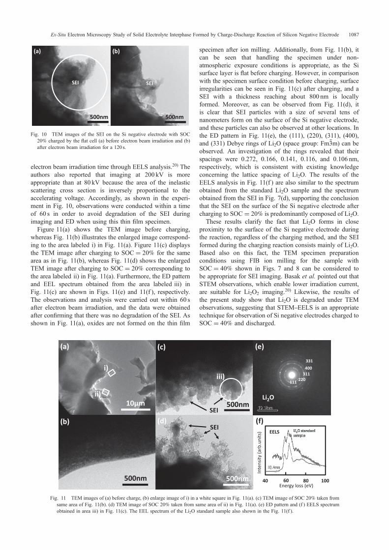
electron beam irradiation time through EELS analysis.20) Theauthors also reported that imaging at 200 kV is moreappropriate than at 80 kV because the area of the inelasticscattering cross section is inversely proportional to theaccelerating voltage. Accordingly, as shown in the experi-ment in Fig. 10, observations were conducted within a timeof 60 s in order to avoid degradation of the SEI duringimaging and ED when using this thin film specimen.
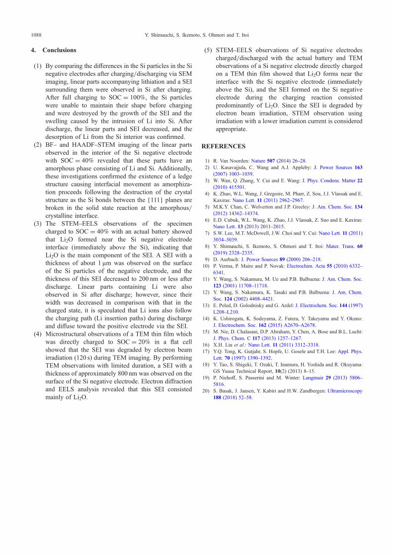
Figure 11(a) shows the TEM image before charging,whereas Fig. 11(b) illustrates the enlarged image correspond-ing to the area labeled i) in Fig. 11(a). Figure 11(c) displaysthe TEM image after charging to SOC = 20% for the samearea as in Fig. 11(b), whereas Fig. 11(d) shows the enlargedTEM image after charging to SOC = 20% corresponding tothe area labeled ii) in Fig. 11(a). Furthermore, the ED patternand EEL spectrum obtained from the area labeled iii) inFig. 11(c) are shown in Figs. 11(e) and 11(f ), respectively.The observations and analysis were carried out within 60 safter electron beam irradiation, and the data were obtainedafter confirming that there was no degradation of the SEI. Asshown in Fig. 11(a), oxides are not formed on the thin film
specimen after ion milling. Additionally, from Fig. 11(b), itcan be seen that handling the specimen under non-atmospheric exposure conditions is appropriate, as the Sisurface layer is flat before charging. However, in comparisonwith the specimen surface condition before charging, surfaceirregularities can be seen in Fig. 11(c) after charging, and aSEI with a thickness reaching about 800 nm is locallyformed. Moreover, as can be observed from Fig. 11(d), itis clear that SEI particles with a size of several tens ofnanometers form on the surface of the Si negative electrode,and these particles can also be observed at other locations. Inthe ED pattern in Fig. 11(e), the (111), (220), (311), (400),and (331) Debye rings of Li2O (space group: Fm�3m) can beobserved. An investigation of the rings revealed that theirspacings were 0.272, 0.166, 0.141, 0.116, and 0.106 nm,respectively, which is consistent with existing knowledgeconcerning the lattice spacing of Li2O. The results of theEELS analysis in Fig. 11(f ) are also similar to the spectrumobtained from the standard Li2O sample and the spectrumobtained from the SEI in Fig. 7(d), supporting the conclusionthat the SEI on the surface of the Si negative electrode aftercharging to SOC = 20% is predominantly composed of Li2O.
These results clarify the fact that Li2O forms in closeproximity to the surface of the Si negative electrode duringthe reaction, regardless of the charging method, and the SEIformed during the charging reaction consists mainly of Li2O.Based also on this fact, the TEM specimen preparationconditions using FIB ion milling for the sample withSOC = 40% shown in Figs. 7 and 8 can be considered tobe appropriate for SEI imaging. Basak et al. pointed out thatSTEM observations, which enable lower irradiation current,are suitable for Li2O2 imaging.20) Likewise, the results ofthe present study show that Li2O is degraded under TEMobservations, suggesting that STEMEELS is an appropriatetechnique for observation of Si negative electrodes charged toSOC = 40% and discharged.
500nm
(a) (b)
SEI SEI
500nm
Fig. 10 TEM images of the SEI on the Si negative electrode with SOC20% charged by the flat cell (a) before electron beam irradiation and (b)after electron beam irradiation for a 120 s.
10μm
500nm
(a)
(b)
i)
500nm
(c)
ii)
iii)
(f)
500nmEnergy loss (eV)
Inte
nsity
(arb
.uni
ts)
40 60 80 100
EELS
(e)
111 220311
400
331
Li2O
SEI
SEI(d)
Fig. 11 TEM images of (a) before charge, (b) enlarge image of i) in a white square in Fig. 11(a). (c) TEM image of SOC 20% taken fromsame area of Fig. 11(b). (d) TEM image of SOC 20% taken from same area of ii) in Fig. 11(a). (e) ED pattern and (f ) EELS spectrumobtained in area iii) in Fig. 11(c). The EEL spectrum of the Li2O standard sample also shown in the Fig. 11(f ).
Ex-Situ Electron Microscopy Study of Solid Electrolyte Interphase Formed by Charge-Discharge Reaction of Silicon Negative Electrode 1087
4. Conclusions
(1) By comparing the differences in the Si particles in the Sinegative electrodes after charging/discharging via SEMimaging, linear parts accompanying lithiation and a SEIsurrounding them were observed in Si after charging.After full charging to SOC = 100%, the Si particleswere unable to maintain their shape before chargingand were destroyed by the growth of the SEI and theswelling caused by the intrusion of Li into Si. Afterdischarge, the linear parts and SEI decreased, and thedesorption of Li from the Si interior was confirmed.
(2) BF and HAADFSTEM imaging of the linear partsobserved in the interior of the Si negative electrodewith SOC = 40% revealed that these parts have anamorphous phase consisting of Li and Si. Additionally,these investigations confirmed the existence of a ledgestructure causing interfacial movement as amorphiza-tion proceeds following the destruction of the crystalstructure as the Si bonds between the {111} planes arebroken in the solid state reaction at the amorphous/crystalline interface.
(3) The STEMEELS observations of the specimencharged to SOC = 40% with an actual battery showedthat Li2O formed near the Si negative electrodeinterface (immediately above the Si), indicating thatLi2O is the main component of the SEI. A SEI with athickness of about 1 µm was observed on the surfaceof the Si particles of the negative electrode, and thethickness of this SEI decreased to 200 nm or less afterdischarge. Linear parts containing Li were alsoobserved in Si after discharge; however, since theirwidth was decreased in comparison with that in thecharged state, it is speculated that Li ions also followthe charging path (Li insertion paths) during dischargeand diffuse toward the positive electrode via the SEI.
(4) Microstructural observations of a TEM thin film whichwas directly charged to SOC = 20% in a flat cellshowed that the SEI was degraded by electron beamirradiation (120 s) during TEM imaging. By performingTEM observations with limited duration, a SEI with athickness of approximately 800 nm was observed on thesurface of the Si negative electrode. Electron diffractionand EELS analysis revealed that this SEI consistedmainly of Li2O.
(5) STEMEELS observations of Si negative electrodescharged/discharged with the actual battery and TEMobservations of a Si negative electrode directly chargedon a TEM thin film showed that Li2O forms near theinterface with the Si negative electrode (immediatelyabove the Si), and the SEI formed on the Si negativeelectrode during the charging reaction consistedpredominantly of Li2O. Since the SEI is degraded byelectron beam irradiation, STEM observation usingirradiation with a lower irradiation current is consideredappropriate.
REFERENCES
1) R. Van Noorden: Nature 507 (2014) 2628.2) U. Kasavajjula, C. Wang and A.J. Appleby: J. Power Sources 163
(2007) 10031039.3) W. Wan, Q. Zhang, Y. Cui and E. Wang: J. Phys. Condens. Matter 22
(2010) 415501.4) K. Zhao, W.L. Wang, J. Gregoire, M. Pharr, Z. Sou, J.J. Vlassak and E.
Kaxiras: Nano Lett. 11 (2011) 29622967.5) M.K.Y. Chan, C. Wolverton and J.P. Greeley: J. Am. Chem. Soc. 134
(2012) 1436214374.6) E.D. Cubuk, W.L. Wang, K. Zhao, J.J. Vlassak, Z. Suo and E. Kaxiras:
Nano Lett. 13 (2013) 20112015.7) S.W. Lee, M.T. McDowell, J.W. Choi and Y. Cui: Nano Lett. 11 (2011)
30343039.8) Y. Shimauchi, S. Ikemoto, S. Ohmori and T. Itoi: Mater. Trans. 60
(2019) 23282335.9) D. Aurbach: J. Power Sources 89 (2000) 206218.10) P. Verma, P. Maire and P. Novak: Electrochim. Acta 55 (2010) 6332
6341.11) Y. Wang, S. Nakamura, M. Ue and P.B. Balbuena: J. Am. Chem. Soc.
123 (2001) 1170811718.12) Y. Wang, S. Nakamura, K. Tasaki and P.B. Balbuena: J. Am. Chem.
Soc. 124 (2002) 44084421.13) E. Peled, D. Golodnisky and G. Ardel: J. Electrochem. Soc. 144 (1997)
L208L210.14) K. Ushirogata, K. Sodeyama, Z. Futera, Y. Takeyama and Y. Okuno:
J. Electrochem. Soc. 162 (2015) A2670A2678.15) M. Nie, D. Chalasani, D.P. Abraham, Y. Chen, A. Bose and B.L. Lucht:
J. Phys. Chem. C 117 (2013) 12571267.16) X.H. Liu et al.: Nano Lett. 11 (2011) 33123318.17) Y.Q. Tong, K. Gutjahr, S. Hopfe, U. Gosele and T.H. Lee: Appl. Phys.
Lett. 70 (1997) 13901392.18) Y. Tao, S. Shigeki, T. Ozaki, T. Inamura, H. Yoshida and R. Okuyama:
GS Yuasa Technical Report, 10(2) (2013) 815.19) P. Niehoff, S. Passerini and M. Winter: Langmuir 29 (2013) 5806
5816.20) S. Basak, J. Jansen, Y. Kabiri and H.W. Zandbergen: Ultramicroscopy
188 (2018) 5258.
Y. Shimauchi, S. Ikemoto, S. Ohmori and T. Itoi1088