ewd-900-hdtc - datasheet.octopart.com
TRANSCRIPT

EWD-900-HDTC
Embedding the wireless future..
128 channel, Half-Duplex 868/915 MHz76.8 kbit/sec FSK Data Transceiver
Typical Applications Features
S
• Asset Tracking • Wireless Sensors • Home Automation • Remote Control • Automated Meter Reading • Remote Data Acquisition • Building Automation
• 500+ feet of range (outdoors line-of-sight) • 3V very low-power operation • .3 to 76.8 kbit/second data rate • No special encoding required to use with
UART • Small DIP form-factor - .7” x .7” x .15” • Unlicensed operation in the US and UK • Factory set 32-bit unique ID is perfect for
network applications • Very Low Cost in Large Volumes • Development tools including API source
code available
Description
ummary Electrical Specifications
Patent Pending The EWD-900-FDTC is a fully integrated half duplex wireless FSK data transceiver. The basic design of the transceiver is frequency-scaleable from 300MHz to 1GHz, allowing operation in countries around the world. The transceiver can operate on 128 channels in the 902-928MHz unlicensed band. It contains built in data encoding and decoding, simplifying the interface and software of the host processor. A typical circuit will consist of a low-cost microcontroller, a power source, and an antenna. The transceiver requires
a
no external RF components with the exception of50-ohm antenna. PreliminaryTa=25°C Parameter Min. Typ. Max.
Units
Operating Frequency - US 902 915 928 MHz Channels – US operation 128 Operating Frequency – UK 868 870 MHz Channels – UK operation 20 TX Output Power 0 5 dBm RX Sensitivity(900MHz) 600 baud Manchester
-97.6 dBm
RX Sensitivity(868MHz) 600 Baud Manchester
-100.6 dBm
Operating Voltage 2.7 3.0 3.3 VDC Operating Current-TX 0dBm 16 mA Operating Current-TX 4dBm 24 mA Operating Current-RX 9.8 mA Data Rate 0.6 76.8 Kbit/sec TX-RX Switch Time 150 uSec
- i -

Document Control Created By Steve Montgomery 10/30/02 Engineering Review Marketing Review Approved - Engineering Approved - Marketing Revision History Revision Author Date Description 1.0 SJM 10/30/01 Document Created 1.1 SJM 11/18/02 Module pin-out diagram and table corrected
- ii -

Table of Contents
Typical Applications ............................................................................................ i Summary Electrical Specifications .................................................................... i Features................................................................................................................ i Description ........................................................................................................... i Document Control............................................................................................... ii Revision History.................................................................................................. ii Table of Figures ................................................................................................. iii Pin Out Diagram..................................................................................................1
Pin Description....................................................................................................1
Mechanical Drawing ...........................................................................................2
Absolute Maximum Ratings...............................................................................2
Detailed Electrical Specifications......................................................................2 AC Specifications – RX.................................................................................................. 2 AC Specifications – TX.................................................................................................. 3 AC Specifications – System Timing............................................................................... 4 DC Specifications ........................................................................................................... 4
Circuit Description..............................................................................................5
Example Application Circuit ..............................................................................7
Related Documentation......................................................................................8
Ordering Information ..........................................................................................8
- ii -

Table of Figures
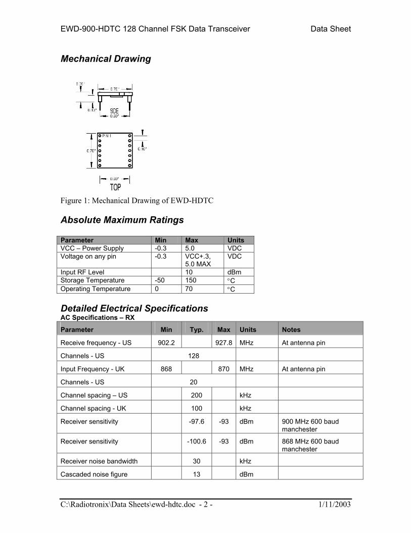
Figure 1: Mechanical Drawing of EWD-HDTC................................................................. 2
Figure 2 EWD-HDTC Internal Block Diagram.................................................................. 5
- iii -
EWD-900-HDTC 128 Channel FSK Data Transceiver Data Sheet
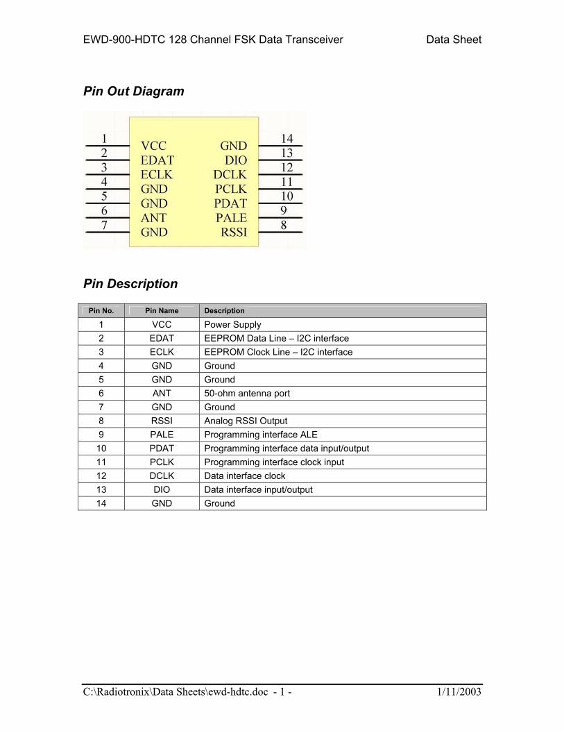
Pin Out Diagram
Pin Description
Pin No. Pin Name Description
1 VCC Power Supply 2 EDAT EEPROM Data Line – I2C interface 3 ECLK EEPROM Clock Line – I2C interface 4 GND Ground 5 GND Ground 6 ANT 50-ohm antenna port 7 GND Ground 8 RSSI Analog RSSI Output 9 PALE Programming interface ALE 10 PDAT Programming interface data input/output 11 PCLK Programming interface clock input 12 DCLK Data interface clock 13 DIO Data interface input/output 14 GND Ground
C:\Radiotronix\Data Sheets\ewd-hdtc.doc - 1 - 1/11/2003
EWD-900-HDTC 128 Channel FSK Data Transceiver Data Sheet
Mechanical Drawing
Figure 1: Mechanical Drawing of EWD-HDTC Absolute Maximum Ratings Parameter Min Max Units VCC – Power Supply -0.3 5.0 VDC Voltage on any pin -0.3 VCC+.3,
5.0 MAX VDC
Input RF Level 10 dBm Storage Temperature -50 150 °C Operating Temperature 0 70 °C Detailed Electrical Specifications AC Specifications – RX
Parameter Min Typ. Max Units Notes
Receive frequency - US 902.2 927.8 MHz At antenna pin
Channels - US 128
Input Frequency - UK 868 870 MHz At antenna pin
Channels - US 20
Channel spacing – US 200 kHz
Channel spacing - UK 100 kHz
Receiver sensitivity -97.6 -93 dBm 900 MHz 600 baud manchester
Receiver sensitivity -100.6 -93 dBm 868 MHz 600 baud manchester
Receiver noise bandwidth 30 kHz
Cascaded noise figure 13 dBm
C:\Radiotronix\Data Sheets\ewd-hdtc.doc - 2 - 1/11/2003

EWD-900-HDTC 128 Channel FSK Data Transceiver Data Sheet
Maximum input power 10 dBm 2.4kBaud Manchester encoded data, BER=10-3
Input IP3 -18 dBm 2.4kBaud Manchester encoded data, BER=10-3
Input Impedance 50 Ohms No matching required
LO Leakage -57 dBm 50-ohm termination at ANT
Adjacent channel rejection TDB40 dBc
dBc
Fc +/-200kHz
Intermediate Frequency (IF) 150 KHz
IF Bandwidth 175 KHz
RSSI Dynamic Range -105 -50 DBm
RSSI Accuracy ±6 DB
RSSI Linearity ±2 DB
Turn-on time 11 128 Bauds Turn-on time is determined by demodulator settling time
AC Specifications – TX
Parameter Min Typ. Max Units Notes
Transmit Frequency -US 902.2 927.8 MHz
Channels - US 128
Channel Spacing - US 200 kHz
Transmit Frequency -UK 868 870 MHz
Channels - UK 20
Channel Spacing - UK 100 kHz
Center frequency error 5 10 ppm 915 MHz, 25°C, using calibration data from EEPROM
Data Rate .3 76.8 kBit/sec
Frequency Deviation 0 65 kHz Fdev is set corresponding to data rate
Output Power -20 -1.3 5 dBm 900 MHz
Into 50 ohm load
Output Power -20 -0.7 5 dBm 868 MHz
Into 50 ohm load
C:\Radiotronix\Data Sheets\ewd-hdtc.doc - 3 - 1/11/2003

EWD-900-HDTC 128 Channel FSK Data Transceiver Data Sheet
Output Impedance 50 Ohms
Carrier phase noise -85 dBc Into 50 ohm load
Harmonic Output -20 -40
dBc dBc
Into 50 ohm load
AC Specifications – System Timing
Parameter Min Typ. Max Units Notes
Turn-on time - TX TBD mSec
Turn-on time – RX TBD mSec
Wake-up time TBD uSec Wake-up from sleep
TX->RX switch time TBD uSec
RX->TX switch time TBD uSec
Channel Change Time 200 uSec Up to 1MHz frequency step
DC Specifications
Parameter Min Typ. Max Units Notes
Supply voltage 2.1 3.0 3.6 VDC Operating limits
Receive current consumption 9.6 96
mA uA
Continuous operation Polled operation
Transmit current consumption Po= -20 dBm Po= -5 dBm Po= 0 dBm Po= 5 dBm
8.6 13.8 16.5 25.4
mA mA mA mA
Output into 50 ohm load
PLL only current consumption 6 mA
Power down current consumption
0.2 TBD uA
Vih – Logic high level input
Vil – Logic low level input
Voh – Logic high level output
Vol – Logic low level output
0.7*Vcc
0
2.5
0
Vcc
0.3*Vcc
Vcc
.4
VDC
VDC
VDC
VDC
C:\Radiotronix\Data Sheets\ewd-hdtc.doc - 4 - 1/11/2003

EWD-900-HDTC 128 Channel FSK Data Transceiver Data Sheet
Circuit Description
IFBLOCK DEMOD
LNA
MIXER
Receive Chain
RXTX
PLL
2
3
RSSI
CO
NTR
OL
ECLKEDAT
EEPR
OM
ANT PIN
TRANSMIT CHAIN
LO
Figure 2 EWD-HDTC Internal Block Diagram
A simplified block diagram of the EWD-HDTC module is shown in Figure 2. The module contains an internal antenna switch, and can operate in one of four modes: TX, RX, sleep, and shutdown. In transmit mode, the local oscillator (LO) is switched to the power amp (PA), generating the transmit carrier. The PLL provides closed-loop frequency control of the carrier. The incoming data stream is used to frequency modulate the carrier. Modulation is precisely controlled by the PLL by switching between two reference frequencies corresponding to the two possible states of the data input line. Data can be transmitted in NRZ or Manchester form. The control block contains a built-in Manchester encoder, simplifying the requirements of the external microcontroller. In receive mode, the module operates like a traditional super heterodyne receiver. The LO is switched to the receive mixer in order to down convert the incoming RF signal to a 150 kHz intermediate frequency. The IF block amplifies and filters the down converted signal in preparation for demodulation. Clock extraction and synchronization is performed on the demodulated data by the control block. The receiver supports NRZ and Manchester encoded data. The on-board PLL allows fine-frequency adjustments to be made to the carrier frequency, eliminating the need for on-board trimmer capacitors and temperature controlled crystal oscillators.
C:\Radiotronix\Data Sheets\ewd-hdtc.doc - 5 - 1/11/2003

EWD-900-HDTC 128 Channel FSK Data Transceiver Data Sheet
A unique feature of the module is the on-board EEPROM. The EEPROM contains a unique 32-bit serial number and calibration data. The calibration data is used to correct for frequency errors generated by the crystal and by temperature deviation from 25 degrees C. For more information on using information from the EEPROM, please refer to “EWD-HDTC USER’S MANUAL”. The EWD-HDTC provides a very simple microcontroller interface. The module is programmed by a 3-wire serial interface, and data is sent and received to and from the module using a 2-wire serial interface. The RSSI pin provides an analog voltage that is proportional to the incoming received signal in dB. Programming the EWD-HDTC is very simple. We provide a complete API for most microcontrollers that is written in C. For details on the API please refer to “EWD-HDTC USER’S MANUAL”.
C:\Radiotronix\Data Sheets\ewd-hdtc.doc - 6 - 1/11/2003
EWD-900-HDTC 128 Channel FSK Data Transceiver Data Sheet
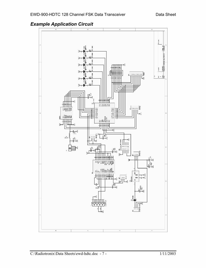
Example Application Circuit
C:\Radiotronix\Data Sheets\ewd-hdtc.doc - 7 - 1/11/2003

EWD-900-HDTC 128 Channel FSK Data Transceiver Data Sheet
C:\Radiotronix\Data Sheets\ewd-hdtc.doc - 8 - 1/11/2003
Related Documentation
• EWD-HDTC USER’S GUIDE (Available November 21, 2002) Ordering Information PRODUCT ORDER CODE EWD-900-HDTC 100-900-06A