evaluation kit low-cost precision sensor signal … low-cost precision sensor signal conditioner 4...
TRANSCRIPT

MA
X1
45
2
Low-Cost Precision SensorSignal Conditioner
________________________________________________________________ Maxim Integrated Products 1
19-1829; Rev 1; 6/01
EVALUATION KIT
AVAILABLE
General DescriptionThe MAX1452 is a highly integrated analog-sensor sig-nal processor optimized for industrial and process con-trol applications utilizing resistive element sensors.The MAX1452 provides amplification, calibration, andtemperature compensation that enables an overall per-formance approaching the inherent repeatability of thesensor. The fully analog signal path introduces noquantization noise in the output signal while enablingdigitally controlled trimming with the integrated 16-bitDACs. Offset and span are calibrated using 16-bitDACs, allowing sensor products to be truly inter-changeable.
The MAX1452 architecture includes a programmablesensor excitation, a 16-step programmable-gain ampli-fier (PGA), a 768-byte (6144 bits) internal EEPROM,four 16-bit DACs, an uncommitted op amp, and an on-chip temperature sensor. In addition to offset and spancompensation. The MAX1452 provides a unique tem-perature compensation strategy for offset TC andFSOTC that was developed to provide a remarkabledegree of flexibility while minimizing testing costs.
The MAX1452 is packaged for the commercial, industri-al, and automotive temperature ranges in 16-pin SSOPpackages.
CustomizationMaxim can customize the MAX1452 for high-volumededicated applications. Using our dedicated cell libraryof more than 2000 sensor-specific functional blocks,Maxim can quickly provide a modified MAX1452 solu-tion. Contact Maxim for further information.
ApplicationsPressure SensorsTransducers and Transmitters Strain GaugesPressure Calibrators and ControllersResistive Elements SensorsAccelerometersHumidity Sensors
Outputs Supported4–20mA0 to +5V (Rail-to-Rail®)+0.5V to +4.5V Ratiometric+2.5V to ±2.5V
Features Provides Amplification, Calibration, and
Temperature Compensation
Accommodates Sensor Output Sensitivities from 1mV/V to 40mV/V
Single Pin Digital Programming
No External Trim Components Required
16-Bit Offset and Span Calibration Resolution
Fully Analog Signal Path
On-Chip Lookup Table Supports MultipointCalibration Temperature Correction
Supports Both Current and Voltage BridgeExcitation
Fast 3.2kHz Frequency Response
On-Chip Uncommitted Op Amp
Secure-Lock™ Prevents Data Corruption
Low 2mA Current Consumption
Rail-to-Rail is a trademark of Nippon Motorola Ltd.Secure-Lock is a trademark of Maxim Integrated Products.
16
15
14
13
12
11
10
9
1
2
3
4
5
6
7
8
ISRC FSOTC
AMP+
AMP-
AMPOUT
CLK1M
DIO
UNLOCK
VDDF
TOP VIEW
MAX1452(NOT TO SCALE)
SSOP
OUT
VSS
INP
INM
BDR
VDD
TEST
Pin Configuration
Ordering Information
16 SSOP
PIN-PACKAGETEMP. RANGE
0°C to +70°CMAX1452CAE
PART
16 SSOP-40°C to +85°CMAX1452EAE
16 SSOP-40°C to +125°CMAX1452AAE
Dice*0°C to +70°CMAX1452C/D
*Dice are tested at TA = +25°C, DC parameters only.
A detailed block diagram appears at the end of data sheet.
For pricing, delivery, and ordering information, please contact Maxim/Dallas Direct! at 1-888-629-4642, or visit Maxim’s website at www.maxim-ic.com.
MA
X1
45
2
Low-Cost Precision SensorSignal Conditioner
2 _______________________________________________________________________________________
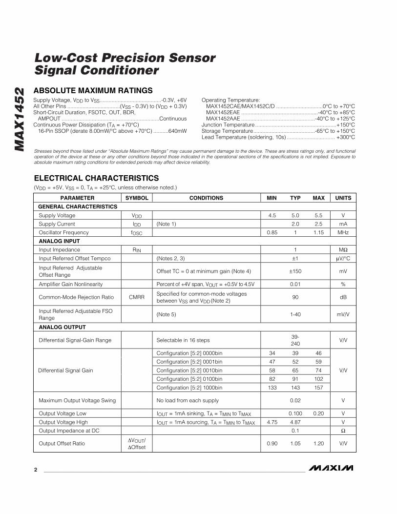
ABSOLUTE MAXIMUM RATINGS
ELECTRICAL CHARACTERISTICS(VDD = +5V, VSS = 0, TA = +25°C, unless otherwise noted.)
Stresses beyond those listed under “Absolute Maximum Ratings” may cause permanent damage to the device. These are stress ratings only, and functionaloperation of the device at these or any other conditions beyond those indicated in the operational sections of the specifications is not implied. Exposure toabsolute maximum rating conditions for extended periods may affect device reliability.
Supply Voltage, VDD to VSS.........................................-0.3V, +6VAll Other Pins ...................................(VSS - 0.3V) to (VDD + 0.3V)Short-Circuit Duration, FSOTC, OUT, BDR,
AMPOUT .................................................................ContinuousContinuous Power Dissipation (TA = +70°C)
16-Pin SSOP (derate 8.00mW/°C above +70°C) ..........640mW
Operating Temperature:MAX1452CAE/MAX1452C/D ...............................0°C to +70°CMAX1452EAE ...................................................-40°C to +85°CMAX1452AAE .................................................-40°C to +125°C
Junction Temperature ......................................................+150°CStorage Temperature.........................................-65°C to +150°CLead Temperature (soldering, 10s) ................................ +300°C
PARAMETER SYMBOL CONDITIONS MIN TYP MAX UNITS
GENERAL CHARACTERISTICS
Supply Voltage VDD 4.5 5.0 5.5 V
Supply Current IDD (Note 1) 2.0 2.5 mA
Oscillator Frequency fOSC 0.85 1 1.15 MHz
ANALOG INPUT
Input Impedance RIN 1 MΩInput Referred Offset Tempco (Notes 2, 3) ±1 µV/°C
Input Referred AdjustableOffset Range
Offset TC = 0 at minimum gain (Note 4) ±150 mV
Amplifier Gain Nonlinearity P er cent of + 4V sp an, V OU T = + 0.5V to 4.5V 0.01 %
Common-Mode Rejection Ratio CMRRSpecified for common-mode voltagesbetween VSS and VDD
(Note 2)90 dB
Input Referred Adjustable FSORange
(Note 5) 1-40 mV/V
ANALOG OUTPUT
Differential Signal-Gain Range Selectable in 16 steps39-240
V/V
Configuration [5:2] 0000bin 34 39 46
Configuration [5:2] 0001bin 47 52 59
Configuration [5:2] 0010bin 58 65 74
Configuration [5:2] 0100bin 82 91 102
Differential Signal Gain
Configuration [5:2] 1000bin 133 143 157
V/V
Maximum Output Voltage Swing No load from each supply 0.02 V
Output Voltage Low IOUT = 1mA sinking, TA = TMIN to TMAX 0.100 0.20 V
Output Voltage High IOUT = 1mA sourcing, TA = TMIN to TMAX 4.75 4.87 V
Output Impedance at DC 0.1 Ω
Output Offset Ratio∆VOUT/∆Offset
0.90 1.05 1.20 V/V

MA
X1
45
2
Low-Cost Precision SensorSignal Conditioner
_______________________________________________________________________________________ 3
ELECTRICAL CHARACTERISTICS (continued)(VDD = +5V, VSS = 0, TA = +25°C, unless otherwise noted.)
PARAMETER SYMBOL CONDITIONS MIN TYP MAX UNITS
Output Offset TC Ratio∆V OU T/
∆Offset TC 0.9 1 1.2 V/V
Step Response and IC(63% Final Value)
150 µs
Maximum Capacitive Load 1 µF
Output NoiseDC to 1kHz (gain = minimum, sourceimpedance = 5kΩ VDDF filter)
0.5 m V RMS
BRIDGE DRIVE
Bridge Current IBDR RL = 1.7kΩ 0.1 0.5 2 mA
Current Mirror Ratio AA RISOURCE = internal 10 12 14 A/A
VSPAN Range (Span Code) TA = TMIN to TMAX 4000 C000 hex
DIGITAL–TO–ANALOG CONVERTERS
DAC Resolution 16 bits
ODAC Bit Weight∆VOUT/∆Code
DAC reference = VDD = +5.0V 76 µV/bit
OTCDAC Bit Weight∆VOUT/∆Code
DAC reference = VBDR = +2.5V 38 µV/bit
FSODAC Bit Weight∆VOUT/∆Code
DAC reference = VDD = +5.0V 76 µV/bit
FSOTCDAC Bit Weight∆VOUT/∆Code
DAC reference = VBDR = +2.5V 38 µV/bit
COARSE OFFSET DAC
IRODAC Resolution Including sign 4 bits
IRODAC Bit Weight∆VOUT/∆Code
Input referred, DAC reference =VDD = +5.0V (Note 6)
9 mV/bit
FSOTC BUFFER
Minimum Output Voltage Swing No loadVSS +
0.1V
Maximum Output Voltage Swing No load V D D - 1.0 V
Current Drive VFSOTC = +2.5V -40 +40 µA
INTERNAL RESISTORS
Current-Source ReferenceResistor
RISRC 75 kΩ
C ur r ent- S our ce Refer enceResi stor Tem p er atur e C oeffi ci ent
∆RIS RC 1300 p p m/°C
FSOTC Resistor RFTC 75 kΩ
FSOTC Resistor Tem p er atur eC oeffi ci ent
∆RFTC 1300 p p m/°C

MA
X1
45
2
Low-Cost Precision SensorSignal Conditioner
4 _______________________________________________________________________________________
Note 1: Excludes sensor or load current.Note 2: All electronics temperature errors are compensated together with sensors errors.Note 3: The sensor and the MAX1452 must be at the same temperature during calibration and use.Note 4: This is the maximum allowable sensor offset.Note 5: This is the sensor's sensitivity normalized to its drive voltage, assuming a desired full span output of +4V and a bridge volt-
age of +2.5V.Note 6: Bit weight is ratiometric to VDD.Note 7: Programming of the EEPROM at room temperature is recommended.Note 8: Allow a minimum of 6ms elapsed time before sending any command.
ELECTRICAL CHARACTERISTICS (continued)(VDD = +5V, VSS = 0, TA = +25°C, unless otherwise noted.)
PARAMETER SYMBOL CONDITIONS MIN TYP MAX UNITS
TEMPERATURE-TO-DIGITAL CONVERTER
Temperature ADC Resolution 8 bits
Offset ±3 LSB
Gain 1.45 °C/bit
Nonlinearity ±0.5 LSB
Lowest Digital Output 00 hex
Highest Digital Output AF hex
UNCOMMITTED OP AMP
Open Loop Gain RL = 100kΩ 90 dB
Input Common-Mode Range VSS VDD V
Output Swing No load, TA = TMIN to TMAXVSS +0.02
VDD -0.02
V
Output Voltage High 1mA source, TA = TMIN to TMAX 4.85 4.90 V
Output Voltage Low 1mA sink, TA = TMIN to TMAX 0.05 0.15 V
Offset VIN+ = +2.5V, unity gain buffer -20 +20 mV
Unity Gain Bandwidth 2 MHz
EEPROM
Maximum Erase/Write Cycles (Note 7) 10k Cycles
Minimum Erase Time (Note 8) 6 ms
MA
X1
45
2
Low-Cost Precision SensorSignal Conditioner
_______________________________________________________________________________________ 5
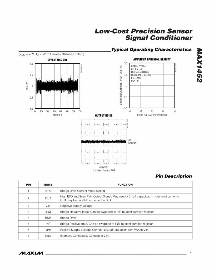
Typical Operating Characteristics(VDD = +5V, TA = +25°C, unless otherwise noted.)
PIN NAME FUNCTION
1 ISRC Bridge Drive Current Mode Setting
2 OUTHigh ESD and Scan Path Output Signal. May need a 0.1µF capacitor, in noisy environments.OUT may be parallel connected to DIO.
3 VSS Negative Supply Voltage
4 INM Bridge Negative Input. Can be swapped to INP by configuration register.
5 BDR Bridge Drive
6 INP Bridge Positive Input. Can be swapped to INM by configuration register.
7 VDD Positive Supply Voltage. Connect a 0.1µF capacitor from VDD to VSS.
8 TEST Internally Connected. Connect to VSS.
Pin Description
OFFSET DAC DNL
MAX
1452
toc0
1
DAC CODE
DNL
(mV)
0 30k 40k10k 20k 50k 60k 70k
5.0
2.5
0
-2.5
-5.0
5.0
2.5
0
-2.5
-5.0
AMPLIFIER GAIN NONLINEARITY
MAX
1452
toc0
2
INPUT VOLTAGE [INP-INM] (mV)
OUTP
UT E
RROR
FRO
M S
TRAI
GHT
LINE
(mV)
-50 0-25 25 50
ODAC = 6800hexOTCDAC = 0FSODAC = 4000hexFSOTCDAC = 8000hexIRO = 2hexPGA = 0
OUTPUT NOISE
MAX
1452
toc0
3
400µs/divC = 4.7µF, RLOAD = 1kΩ
OUT10mV/div
MA
X1
45
2
Detailed DescriptionThe MAX1452 provides amplification, calibration, andtemperature compensation to enable an overall perfor-mance approaching the inherent repeatability of thesensor. The fully analog signal-path introduces noquantization noise in the output signal while enablingdigitally controlled trimming with the integrated 16-bitDACs. Offset and span can be calibrated to within±0.02% of span.
The MAX1452 architecture includes a programmablesensor excitation, a 16-step programmable-gain ampli-fier (PGA), a 768-byte (6144 bits) internal EEPROM, four16-bit DACs, an uncommitted op amp, and an on-chiptemperature sensor.The MAX1452 also provides aunique temperature compensation strategy for offsetTC and FSOTC that was developed to provide aremarkable degree of flexibility while minimizing testingcosts.
The customer can select from one to 114 temperaturepoints to compensate their sensor. This allows the lati-tude to compensate a sensor with a simple first orderlinear correction or match an unusual temperaturecurve. Programming up to 114 independent 16-bit EEP-ROM locations corrects performance in 1.5°C tempera-ture increments over a range of -40°C to +125°C. Forsensors that exhibit a characteristic temperature perfor-mance, a select number of calibration points can beused with a number of preset values that define thetemperature curve. In cases where the sensor is at adifferent temperature than the ASIC, the MAX1452 usesthe sensor bridge itself to provide additional tempera-ture correction.
The single pin, serial Digital Input-Output (DIO) commu-nication architecture and the ability to timeshare itsactivity with the sensor’s output signal enables outputsensing and calibration programming on a single lineby parallel connecting OUT and DIO. The MAX1452provides a Secure-Lock feature that allows the cus-tomer to prevent modification of sensor coefficients andthe 52-byte user definable EEPROM data after the sen-sor has been calibrated. The Secure-Lock feature alsoprovides a hardware override to enable factory reworkand recalibration by assertion of logic high on theUNLOCK pin.
The MAX1452 allows complete calibration and sensorverification to be performed at a single test station.Once calibration coefficients have been stored in theASIC, the customer can choose to retest in order to ver-ify performance as part of a regular QA audit or to gen-erate final test data on individual sensors.
The MAX1452’s low current consumption and the inte-grated uncommitted op amp enables a 4–20mA outputsignal format in a sensor that is completely poweredfrom a 2-wire current loop. Frequency response can beuser-adjusted to values lower than the 3.2kHz band-width by using the uncommitted op amp and simplepassive components.
The MAX1452 (Figure 1) provides an analog amplifica-tion path for the sensor signal. It also uses an analogarchitecture for first-order temperature correction. Adigitally controlled analog path is then used for nonlin-ear temperature correction. Calibration and correctionis achieved by varying the offset and gain of a pro-grammable-gain-amplifier (PGA) and by varying thesensor bridge excitation current or voltage. The PGA
Low-Cost Precision SensorSignal Conditioner
6 _______________________________________________________________________________________
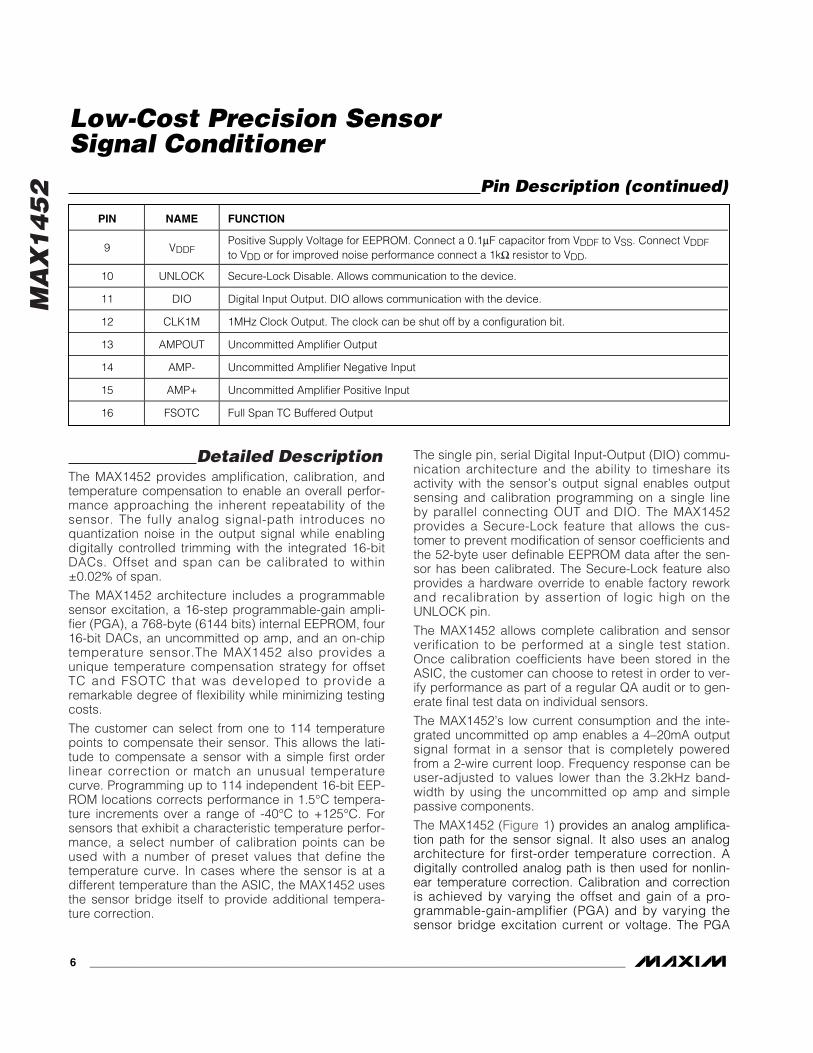
Pin Description (continued)
PIN NAME FUNCTION
9 VDDFPositive Supply Voltage for EEPROM. Connect a 0.1µF capacitor from VDDF to VSS. Connect VDDFto VDD or for improved noise performance connect a 1kΩ resistor to VDD.
10 UNLOCK Secure-Lock Disable. Allows communication to the device.
11 DIO Digital Input Output. DIO allows communication with the device.
12 CLK1M 1MHz Clock Output. The clock can be shut off by a configuration bit.
13 AMPOUT Uncommitted Amplifier Output
14 AMP- Uncommitted Amplifier Negative Input
15 AMP+ Uncommitted Amplifier Positive Input
16 FSOTC Full Span TC Buffered Output
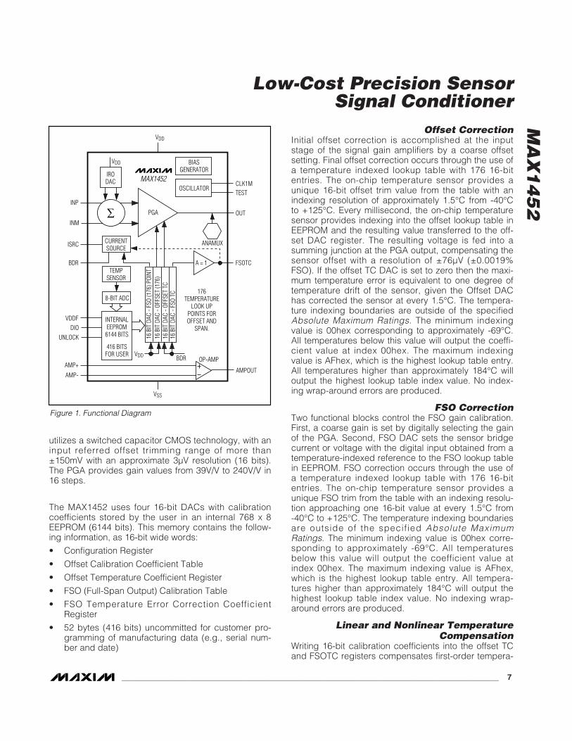
utilizes a switched capacitor CMOS technology, with aninput referred offset trimming range of more than±150mV with an approximate 3µV resolution (16 bits).The PGA provides gain values from 39V/V to 240V/V in16 steps.
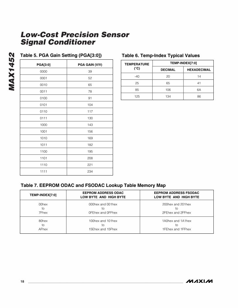
The MAX1452 uses four 16-bit DACs with calibrationcoefficients stored by the user in an internal 768 x 8EEPROM (6144 bits). This memory contains the follow-ing information, as 16-bit wide words:
• Configuration Register
• Offset Calibration Coefficient Table
• Offset Temperature Coefficient Register
• FSO (Full-Span Output) Calibration Table
• FSO Temperature Error Correction CoefficientRegister
• 52 bytes (416 bits) uncommitted for customer pro-gramming of manufacturing data (e.g., serial num-ber and date)
Offset CorrectionInitial offset correction is accomplished at the inputstage of the signal gain amplifiers by a coarse offsetsetting. Final offset correction occurs through the use ofa temperature indexed lookup table with 176 16-bitentries. The on-chip temperature sensor provides aunique 16-bit offset trim value from the table with anindexing resolution of approximately 1.5°C from -40°Cto +125°C. Every millisecond, the on-chip temperaturesensor provides indexing into the offset lookup table inEEPROM and the resulting value transferred to the off-set DAC register. The resulting voltage is fed into asumming junction at the PGA output, compensating thesensor offset with a resolution of ±76µV (±0.0019%FSO). If the offset TC DAC is set to zero then the maxi-mum temperature error is equivalent to one degree oftemperature drift of the sensor, given the Offset DAChas corrected the sensor at every 1.5°C. The tempera-ture indexing boundaries are outside of the specifiedAbsolute Maximum Ratings. The minimum indexingvalue is 00hex corresponding to approximately -69°C.All temperatures below this value will output the coeffi-cient value at index 00hex. The maximum indexingvalue is AFhex, which is the highest lookup table entry.All temperatures higher than approximately 184°C willoutput the highest lookup table index value. No index-ing wrap-around errors are produced.
FSO CorrectionTwo functional blocks control the FSO gain calibration.First, a coarse gain is set by digitally selecting the gainof the PGA. Second, FSO DAC sets the sensor bridgecurrent or voltage with the digital input obtained from atemperature-indexed reference to the FSO lookup tablein EEPROM. FSO correction occurs through the use ofa temperature indexed lookup table with 176 16-bitentries. The on-chip temperature sensor provides aunique FSO trim from the table with an indexing resolu-tion approaching one 16-bit value at every 1.5°C from -40°C to +125°C. The temperature indexing boundariesare outside of the specified Absolute MaximumRatings. The minimum indexing value is 00hex corre-sponding to approximately -69°C. All temperaturesbelow this value will output the coefficient value atindex 00hex. The maximum indexing value is AFhex,which is the highest lookup table entry. All tempera-tures higher than approximately 184°C will output thehighest lookup table index value. No indexing wrap-around errors are produced.
Linear and Nonlinear TemperatureCompensation
Writing 16-bit calibration coefficients into the offset TCand FSOTC registers compensates first-order tempera-
MA
X1
45
2
Low-Cost Precision SensorSignal Conditioner
_______________________________________________________________________________________ 7
MAX1452
BIASGENERATOR
OSCILLATOR
16 B
IT D
AC -
OFFS
ET T
C16
BIT
DAC
- OF
FSET
(176
)16
BIT
DAC
- FS
O (1
76) P
OINT
16 B
IT D
AC -
FSO
TC
ANAMUX
FSOTC
176TEMPERATURE
LOOK UPPOINTS FOROFFSET AND
SPAN.
OP-AMP
A = 1
AMPOUT
VSS
OUT
VDD
CLK1MTEST
INTERNALEEPROM
6144 BITS
416 BITSFOR USER
BDR
PGA
VDDF
VDD BDR
DIOUNLOCK
AMP+
AMP-
INP
ISRC
INM
8-BIT ADC
TEMPSENSOR
IRODAC
CURRENTSOURCE
VDD
∑
Figure 1. Functional Diagram

MA
X1
45
2 ture errors. The piezoresistive sensor is powered by acurrent source resulting in a temperature-dependentbridge voltage due to the sensor's temperature resis-tance coefficient (TCR). The reference inputs of the off-set TC DAC and FSOTC DAC are connected to thebridge voltage. The DAC output voltages will track thebridge voltage as it varies with temperature, and byvarying the offset TC and FSOTC digital code a portionof the bridge voltage, which is temperature dependent,is used to compensate the first order temperatureerrors.
The internal feedback resistors (RISRC and RSTC) forFSO temperature compensation are optimized to 75kΩfor silicon piezoresistive sensors. However, since therequired feedback resistor values are sensor depen-dent, external resistors may also be used. The internalresistors selection bit in the configuration registerselects between internal and external feedback resis-tors.
To calculate the required offset TC and FSOTC com-pensation coefficients, two test-temperatures are need-ed. After taking at least two measurements at eachtemperature, calibration software (in a host computer)calculates the correction coefficients and writes them tothe internal EEPROM.
With coefficients ranging from 0000hex to FFFFhex anda +5V reference, each DAC has a resolution of 76µV.Two of the DACs (offset TC and FSOTC) utilize the sen-sor bridge voltage as a reference. Since the sensorbridge voltage is approximately set to +2.5V the FSOTCand offset TC exhibit a step size of less than 38µV.
For high accuracy applications (errors less than0.25%), the first-order offset and FSOTC should becompensated with the offset TC and FSOTC DACs, andthe residual higher order terms with the lookup table.The offset and FSO compensation DACs provideunique compensation values for approximately 1.5°C oftemperature change as the temperature indexes theaddress pointer through the coefficient lookup table.Changing the offset does not effect the FSO, howeverchanging the FSO will affect the offset due to nature ofthe bridge. The temperature is measured on both theMAX1452 die and at the bridge sensor. It is recom-mended to compensate the first-order temperatureerrors using the bridge sensor temperature.
Typical Ratiometric Operating Circuit
Ratiometric output configuration provides an output thatis proportional to the power supply voltage. This outputcan then be applied to a ratiometric ADC to produce adigital value independent of supply voltage.Ratiometricity is an important consideration for battery-operated instruments, automotive, and some industrialapplications.
The MAX1452 provides a high-performance ratiometricoutput with a minimum number of external components(Figure 2). These external components include the fol-lowing:
• One supply bypass capacitor.
• One optional output EMI suppression capacitor.
• Two optional resistors, RISRC and RSTC, for specialsensor bridge types.
Low-Cost Precision SensorSignal Conditioner
8 _______________________________________________________________________________________
Figure 2. Basic Ratiometric Output Configuration
MAX1452
+5V VDD
OUT
GND
RSTC
RISRC0.1µF 0.1µF
INM
TEST VSS
INP
7
9
2
16
1
8 3
BDR VDDF
OUT
5
6
4
FSOTC
ISRC
SENSOR
VDD
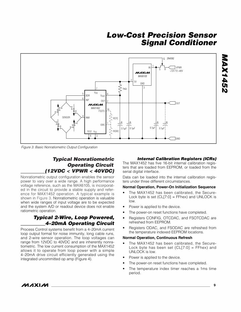
Typical Nonratiometric Operating Circuit
(12VDC < VPWR < 40VDC)Nonratiometric output configuration enables the sensorpower to vary over a wide range. A high performancevoltage reference, such as the MAX6105, is incorporat-ed in the circuit to provide a stable supply and refer-ence for MAX1452 operation. A typical example isshown in Figure 3. Nonratiometric operation is valuablewhen wide ranges of input voltage are to be expectedand the system A/D or readout device does not enableratiometric operation.
Typical 2-Wire, Loop Powered,4–20mA Operating Circuit
Process Control systems benefit from a 4–20mA currentloop output format for noise immunity, long cable runs,and 2-wire sensor operation. The loop voltages canrange from 12VDC to 40VDC and are inherently nonra-tiometric. The low current consumption of the MAX1452allows it to operate from loop power with a simple 4–20mA drive circuit efficiently generated using theintegrated uncommitted op amp (Figure 4).
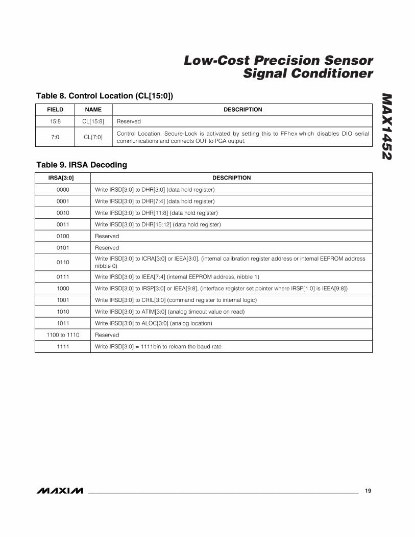
Internal Calibration Registers (ICRs)The MAX1452 has five 16-bit internal calibration regis-ters that are loaded from EEPROM, or loaded from theserial digital interface.
Data can be loaded into the internal calibration regis-ters under three different circumstances.
Normal Operation, Power-On Initialization Sequence
• The MAX1452 has been calibrated, the Secure-Lock byte is set (CL[7:0] = FFhex) and UNLOCK islow.
• Power is applied to the device.
• The power-on reset functions have completed.
• Registers CONFIG, OTCDAC, and FSOTCDAC arerefreshed from EEPROM.
• Registers ODAC, and FSODAC are refreshed fromthe temperature indexed EEPROM locations.
Normal Operation, Continuous Refresh
• The MAX1452 has been calibrated, the Secure-Lock byte has been set (CL[7:0] = FFhex) andUNLOCK is low.
• Power is applied to the device.
• The power-on reset functions have completed.
• The temperature index timer reaches a 1ms timeperiod.
MA
X1
45
2
Low-Cost Precision SensorSignal Conditioner
_______________________________________________________________________________________ 9
MAX1452
VPWR+12V TO +40V
OUT
GND
RSTC
RISRC0.1µF 0.1µF 0.1µF0.1µF
INM
TEST VSS
INP
7
9
2
16
1
8 3
BDR VDDF
OUT
5
6
4
FSOTC
ISRC
SENSOR
MAX6105
5VGND
1
3
IN
2
1kΩVDD
G
S D
2N4392
Figure 3. Basic Nonratiometric Output Configuration

MA
X1
45
2
• Registers CONFIG, OTCDAC, and FSOTCDAC arerefreshed from EEPROM.
• Registers ODAC and FSODAC are refreshed fromthe temperature indexed EEPROM locations.
Calibration Operation, Registers Updated by SerialCommunications
• The MAX1452 has not had the Secure-Lock byteset (CL[7:0] = 00hex) or UNLOCK is high.
• Power is applied to the device.
• The power-on reset functions have completed.
• The registers can then be loaded from the serialdigital interface by use of serial commands. See thesection on Serial I/O and Commands.
Internal EEPROMThe internal EEPROM is organized as a 768 by 8-bitmemory. It is divided into 12 pages, with 64 bytes perpage. Each page can be individually erased. The mem-ory structure is arranged as shown in Table 1. The look-up tables for ODAC and FSODAC are also shown, withthe respective temp-index pointer. Note that the ODACtable occupies a continuous segment, from address000hex to address 15Fhex, whereas the FSODAC tableis divided in two parts, from 200hex to 2FFhex, andfrom 1A0hex to 1FFhex. With the exception of the gen-eral purpose user bytes, all values are 16-bit widewords formed by two adjacent byte locations (high byteand low byte).
The MAX1452 compensates for sensor offset, FSO, andtemperature errors by loading the internal calibrationregisters with the compensation values. These com-pensation values can be loaded to registers directly via
Low-Cost Precision SensorSignal Conditioner
10 ______________________________________________________________________________________
MAX1452
VIN++12V TO +40V
2N2222A
47Ω100kΩ
4.99kΩ
4.99MΩ
1kΩ
100Ω
499kΩ
100kΩ
VIN-
RSTC
RISRC
0.1µF
0.1µF
0.1µF
0.1µF
0.1µFINM
TEST VSS
INP
7
9
16
1
2
13
14
15
8 3
BDR VDDF
VDD5
6
4
FSOTC
ISRCSENSOR
MAX6105
5VOUTGND
1
D
S
G
3
Z1IN
2N4392
2
OUT
AMPOUT
AMP-
AMP+
Figure 4. Basic 4–20mA Output, Loop-Powered Configuration

the serial digital interface during calibration or loadedautomatically from EEPROM at power-on. In this waythe device can be tested and configured during cali-bration and test and the appropriate compensation val-ues stored in internal EEPROM. The device wil l
auto-load the registers from EEPROM and be ready foruse without further configuration after each power-up.The EEPROM is configured as an 8-bit wide array soeach of the 16-bit registers is stored as two 8-bit quan-tities. The configuration register, FSOTCDAC and OTC-
MA
X1
45
2
Low-Cost Precision SensorSignal Conditioner
______________________________________________________________________________________ 11
Table 1. EEPROM Memory Address Map
PAGELOW-BYTE
ADDRESS (hex)HIGH-BYTE
ADDRESS (hex)TEMP-INDEX[7:0]
(hex)CONTENTS
000 001 000
03E 03F 1F
040 041 201
07E 07F 3F
080 081 402
0BE 0BF 5F
0C0 0C1 603
0FE 0FF 7F
100 101 804
13E 13F 9F
140 141 A0
15E 15F AF to FF
ODACLookup Table
160 161 Configuration
162 163 Reserved
164 165 OTCDAC
166 167 Reserved
168 169 FSOTCDAC
16A 16B Control Location
16C 16D
5
17E 17F
180 181
19E 19F
52 General-PurposeUser Bytes
1A0 1A1 806
1BE 1BF 8F
1C0 1C1 907
1FE 1FF AF to FF
200 201 008
23E 23F 1F
240 241 209
27E 27F 3F
280 281 40A
2BE 2BF 5F
2C0 2C1 60B
2FE 2FF 7F
FSODACLookup Table
MA
X1
45
2 DAC registers are loaded from the pre-assigned loca-tions in the EEPROM.
The ODAC and FSODAC are loaded from the EEPROMlookup tables using an index pointer that is a functionof temperature. An ADC converts the integrated tem-perature sensor to an 8-bit value every 1ms. This digi-tized value is then transferred into the temp-indexregister.
The typical transfer function for the temp-index is as fol-lows:
temp-index = 0.69 Temperature (°C) + 47.58
where temp-index is truncated to an 8-bit integer value.Typical values for the temp-index register are given inTable 6.
Note that the EEPROM is byte wide and the registersthat are loaded from EEPROM are 16 bits wide. Thuseach index value points to two bytes in the EEPROM.
Maxim programs all EEPROM locations to FFhex withthe exception of the oscillator frequency setting andSecure-Lock byte. OSC[2:0] is in the ConfigurationRegister (Table 3). These bits should be maintained atthe factory preset values. Programming 00hex in theSecure-Lock byte (CL[7:0] = 00hex), configures theDIO as an asynchronous serial input for calibration andtest purposes.
Communication ProtocolThe DIO serial interface is used for asynchronous serialdata communications between the MAX1452 and ahost calibration test system or computer. The MAX1452will automatically detect the baud rate of the host com-puter when the host transmits the init ial izationsequence. Baud rates between 4800bps and38,400bps can be detected and used regardless of theinternal oscillator frequency setting. Data format isalways 1 start bit, 8 data bits, 1 stop bit and no parity.Communications are only allowed when Secure-Lock isdisabled (i.e., CL[7:0] = 00hex) or the UNLOCK pin isheld high.
Initialization Sequence Sending the initialization sequence shown belowenables the MAX1452 to establish the baud rate thatinitializes the serial port. The initialization sequence isone byte transmission of 01hex, as follows.
1111111101000000011111111
The first start bit 0 initiates the baud rate synchronizationsequence. The 8 data bits 01hex (LSB first) follow thisand then the stop bit, which is indicated above as a 1,
terminates the baud rate synchronization sequence.This initialization sequence on DIO should occur after aperiod of 1ms after stable power is applied to thedevice. This allows time for the power-on reset functionto complete and the DIO pin to be configured bySecure-Lock or the UNLOCK pin.
Reinitialization Sequence The MAX1452 allows for relearning the baud rate. Thereinitialization sequence is one byte transmission ofFFhex, as follows.
11111111011111111111111111
When a serial reinitialization sequence is received, thereceive logic resets itself to its power-up state andwaits for the initialization sequence. The initializationsequence must follow the reinitialization sequence inorder to re-establish the baud rate.
Serial Interface Command FormatAll communication commands into the MAX1452 followa defined format utilizing an interface register set (IRS).The IRS is an 8-bit command that contains both aninterface register set data (IRSD) nibble (4-bit) and aninterface register set address (IRSA) nibble (4-bit). Allinternal calibration registers and EEPROM locations areaccessed for read and write through this interface reg-ister set. The IRS byte command is structured as fol-lows:
IRS[7:0] = IRSD[3:0], IRSA[3:0]
Where:
• IRSA[3:0] is the 4-bit interface register set addressand indicates which register receives the data nib-ble IRSD[3:0].
• IRSA[0] is the first bit on the serial interface after thestart bit.
• IRSD[3:0] is the 4-bit interface register set data.
• IRSD[0] is the fifth bit received on the serial inter-face after the start bit.
The IRS address decoding is shown in Table 9.
Special Command Sequences A special command register to internal logic(CRIL[3:0]) causes execution of special commandsequences within the MAX1452. These commandsequences are listed as CRIL command codes asshown in Table 10.
Write ExamplesA 16-bit write to any of the internal calibration registersis performed as follows:
Low-Cost Precision SensorSignal Conditioner
12 ______________________________________________________________________________________

1) Write the 16 data bits to DHR[15:0] using four byteaccesses into the interface register set.
2) Write the address of the target internal calibrationregister to ICRA[3:0].
3) Write the load internal calibration register (LdICR)command to CRIL[3:0].
When a LdICR command is issued to the CRIL register,the calibration register loaded depends on the addressin the internal calibration register address (ICRA). Table11 specifies which calibration register is decoded.
Erasing and Writing the EEPROMThe internal EEPROM needs to be erased (bytes set toFFhex) prior to programming the desired contents.Remember to save the 3 MSBs of byte 161hex (high-byte of the configuration register) and restore it whenprogramming its contents to prevent modification of thetrimmed oscillator frequency.
The internal EEPROM can be entirely erased with theERASE command, or partial ly erased with thePageErase command (see Table 10, CRIL command).It is necessary to wait 6ms after issuing the ERASE orPageErase command.
After the EEPROM bytes have been erased (value ofevery byte = FFhex), the user can program its contents,following the procedure below:
1) Write the 8 data bits to DHR[7:0] using two byteaccesses into the interface register set.
2) Write the address of the target internal EEPROMlocation to IEEA[9:0] using three byte accesses intothe interface register set.
3) Write the EEPROM write command (EEPW) toCRIL[3:0].
Serial Digital Output When a RdIRS command is written to CRIL[3:0], DIO isconfigured as a digital output and the contents of the
register designated by IRSP[3:0] are sent out as a byteframed by a start bit and a stop bit.
Once the tester finishes sending the RdIRS command,it must three-state its connection to DIO to allow theMAX1452 to drive the DIO line. The MAX1452 will three-state DIO high for 1 byte time and then drive with thestart bit in the next bit period followed by the data byteand stop bit. The sequence is shown in Figure 5.
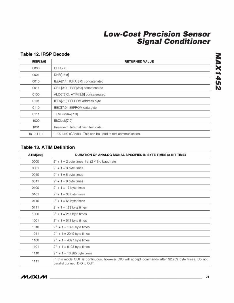
The data returned on a RdIRS command depends onthe address in IRSP. Table 12 defines what is returnedfor the various addresses.
Multiplexed Analog Output When a RdAlg command is written to CRIL[3:0] theanalog signal designated by ALOC[3:0] is asserted onthe OUT pin. The duration of the analog signal is deter-mined by ATIM[3:0] after which the pin reverts to three-state. While the analog signal is asserted in the OUTpin, DIO is simultaneously three-stated, enabling a par-allel wiring of DIO and OUT. When DIO and OUT areconnected in parallel, the host computer or calibrationsystem must three-state its connection to DIO afterasserting the stop bit. Do not load the OUT line whenreading internal signals, such as BDR, FSOTC...etc.
The analog output sequence with DIO and OUT isshown in Figure 6.
The duration of the analog signal is controlled byATIM[3:0] as given in Table 13.
The analog signal driven onto the OUT pin is deter-mined by the value in the ALOC register. The signalsare specified in Table 14.
Test System ConfigurationThe MAX1452 is designed to support an automatedproduction test system with integrated calibration andtemperature compensation. Figure 7 shows the imple-mentation concept for a low-cost test system capableof testing many transducer modules connected in par-
MA
X1
45
2
Low-Cost Precision SensorSignal Conditioner
______________________________________________________________________________________ 13
DRIVEN BY TESTER DRIVEN BY MAX1452
THREE-STATE NEED WEAK
PULLUP
THREE-STATE NEED WEAK
PULLUP
START-BITLSB
START-BITLSB
MSB
STOP-BIT
MSB
STOP-BIT1 1 1 1 1 0 1 0 0 1 1 0 1 0 1 1 1 1 1 1 1 1 1 1 0 0 0 0 0 1 0 0 0 1 1 1 1 1 1 1 1 1 1 1DIO
Figure 5. DIO Output Data Format

MA
X1
45
2
allel. The MAX1452 allows for a high degree of flexibili-ty in system calibration design. This is achieved by useof single-wire digital communication and three-stateoutput nodes. Depending upon specific calibrationrequirements one may connect all the OUTs in parallelor connect DIO and OUT on each individual module.
Sensor Compensation OverviewCompensation requires an examination of the sensorperformance over the operating pressure and tempera-ture range. Use a minimum of two test pressures (e.g.,zero and full-span) and two temperatures. More testpressures and temperatures will result in greater accu-racy. A typical compensation procedure can be sum-marized as follows:
Set reference temperature (e.g., 25°C):
• Initialize each transducer by loading their respec-tive registers with default coefficients (e.g., basedon mean values of offset, FSO and bridge resis-tance) to prevent overload of the MAX1452.
• Set the initial bridge voltage (with the FSODAC) tohalf of the supply voltage. Measure the bridge volt-age using the BDR or OUT pins, or calculate basedon measurements.
• Calibrate the output offset and FSO of the transduc-er using the ODAC and FSODAC, respectively.
• Store calibration data in the test computer orMAX1452 EEPROM user memory.
Set next test temperature:
• Calibrate offset and FSO using the ODAC and FSO-DAC, respectively.
• Store calibration data in the test computer orMAX1452 EEPROM user memory.
• Calculate the correction coefficients.
• Download correction coefficients to EEPROM.
• Perform a final test.
Sensor Calibration and Compensation Example
The MAX1452 temperature compensation design cor-rects both sensor and IC temperature errors. Thisenables the MAX1452 to provide temperature compen-sation approaching the inherent repeatability of thesensor. An example of the MAX1452’s capabilities isshown in Figure 8.
A repeatable piezoresistive sensor with an initial offsetof 16.4mV and a span of 55.8mV was converted into acompensated transducer (utilizing the piezoresistivesensor with the MAX1452) with an offset of 0.5000V anda span of 4.0000V. Nonlinear sensor offset and FSOtemperature errors, which were on the order of 20% to30% FSO, were reduced to under ±0.1% FSO. The fol-lowing graphs show the output of the uncompensatedsensor and the output of the compensated transducer.Six temperature points were used to obtain this result.
MAX1452 Evaluation KitTo expedite the development of MAX1452based transducers and test systems, Maxim has pro-duced the MAX1452 evaluation kit (EV kit). First-timeusers of the MAX1452 are strongly encouraged to usethis kit.
Low-Cost Precision SensorSignal Conditioner
14 ______________________________________________________________________________________
DRIVEN BY TESTER
THREE-STATE NEED WEAK
PULLUP
THREE-STATE NEED WEAK
PULLUP
START-BITLSB
MSB
STOP-BIT
1 1 1 1 1 0 1 0 0 1 1 0 1 0 1 1 1 1 1 1 1 1 1 1 1 1 1 1 1 11 11 1 1 11 1 11 1 1 1 1
THREE-STATE 2ATIM +1 BYTE
TIMES
DIO
OUT VALID OUT
HIGH IMPEDANCE
Figure 6. Analog Output Timing

MA
X1
45
2
Low-Cost Precision SensorSignal Conditioner
______________________________________________________________________________________ 15
The EV kit is designed to facilitate manual program-ming of the MAX1452 with a sensor. It includes the fol-lowing:
1) Evaluation Board with or without a silicon pressuresensor, ready for customer evaluation.
2) Design/Applications Manual, which describes indetail the architecture and functionality of theMAX1452. This manual was developed for testengineers familiar with data acquisition of sensordata and provides sensor compensation algorithmsand test procedures.
3) MAX1452 Communication Software, which enablesprogramming of the MAX1452 from a computerkeyboard (IBM compatible), one module at a time.
4) Interface Adapter, which allows the connection ofthe evaluation board to a PC serial port.
MAX
1452
VOUT
VDD
MODULE 1
DATA DATA
VSS VSS VDDVDD VSS
TEST OVENM
AX14
52
VOUT
MODULE 2
VOUT
DIGITALMULTIPLEXER
+5V
DIO[1:N]
DIO1 DIO2 DION
MAX
1452
VOUT
MODULE N
DVM
Figure 7. Automated Test System Concept

Table 2. Registers
REGISTER DESCRIPTION
CONFIG Configuration Register
ODAC Offset DAC Register
OTCDAC Offset Temperature Coefficient DAC Register
FSODAC Full Span Output DAC Register
FSOTCDAC Full Span Output Temperature Coefficient DAC Register
MA
X1
45
2
Low-Cost Precision SensorSignal Conditioner
16 ______________________________________________________________________________________
80
60
0
6
40
0 4020 60 80 100
RAW SENSOR OUTPUTTA = +25°C
PRESSURE (kPs)
V OUT
(mV)
0
1.0
3.0
2.0
4.0
5.0
0 4020 60 80 100
COMPENSATED TRANSDUCERTA = +25°C
PRESSURE (kPs)
V OUT
(V)
-20.0
10.0
30.0
20.0
-10.0
0.0
UNCOMPENSATED SENSORTEMPERATURE ERROR
TEMPERATURE (°C)
ERRO
R (%
FSO
)
-50 500 100 150
FSO OFFSET
-0.15
-0.05-0.1
0.050
0.10.15
-50 500 100 150
COMPENSATED TRANSDUCER ERROR
TEMPERATURE (°C)
ERRO
R (%
FSO
)
FSO OFFSET
Figure 8. Comparison of an Uncalibrated Sensor and a Calibrated Transducer

MA
X1
45
2
Low-Cost Precision SensorSignal Conditioner
______________________________________________________________________________________ 17
Table 3. Configuration Register (CONFIG[15:0])
FIELD NAME DESCRIPTION
15:13 OSC[2:0] Oscillator frequency setting. Factory preset, do not change.
12 REXT Logic ‘1’ selects external RISRC and RSTC.
11 CLK1M EN Logic ‘1’ enables CLK1M output driver.
10 PGA Sign Logic ‘1’ inverts INM and INP polarity.
9 IRO Sign Logic ‘1’ for positive input referred offset (IRO). Logic ‘0’ for negative input referred offset (IRO).
8:6 IRO[2:0] Input referred coarse offset adjustment.
5:2 PGA[3:0] Programmable gain amplifier setting.
1 ODAC Sign Logic ‘1’ for positive offset DAC output. Logic ‘0’ for negative offset DAC output.
0OTCDAC
SignLogic ‘1’ for positive offset TC DAC output. Logic ‘0’ for negative offset TC DAC output.
Table 4. Input Referred Offset (IRO[2:0])
IRO SIGN, IRO[2:0]INPUT REFERRED OFFSET
CORRECTION AS % OF VDDI N PU T R EF ER R ED O F F SET , CO R R EC T IO N
A T VD D = 5 VD C I N mV
1,111 +1.25 +63
1,110 +1.08 +54
1,101 +0.90 +45
1,100 +0.72 +36
1,011 +0.54 +27
1,010 +0.36 +18
1,001 +0.18 +9
1,000 0 0
0,000 0 0
0,001 -0.18 -9
0,010 -0.36 -18
0,011 -0.54 -27
0,100 -0.72 -36
0,101 -0.90 -45
0,110 -1.08 -54
0,111 -1.25 -63
MA
X1
45
2
Low-Cost Precision SensorSignal Conditioner
18 ______________________________________________________________________________________
Table 7. EEPROM ODAC and FSODAC Lookup Table Memory Map
TEMP-INDEX[7:0]EEPROM ADDRESS ODAC
LOW BYTE AND HIGH BYTEEEPROM ADDRESS FSODACLOW BYTE AND HIGH BYTE
00hexto
7Fhex
000hex and 001hexto
0FEhex and 0FFhex
200hex and 201hexto
2FEhex and 2FFhex
80hexto
AFhex
100hex and 101hexto
15Ehex and 15Fhex
1A0hex and 1A1hexto
1FEhex and 1FFhex
Table 5. PGA Gain Setting (PGA[3:0])
PGA[3:0] PGA GAIN (V/V)
0000 39
0001 52
0010 65
0011 78
0100 91
0101 104
0110 117
0111 130
1000 143
1001 156
1010 169
1011 182
1100 195
1101 208
1110 221
1111 234
Table 6. Temp-Index Typical Values
TEMP-INDEX[7:0]TEMPERATURE(°C) DECIMAL HEXADECIMAL
-40 20 14
25 65 41
85 106 6A
125 134 86
MA
X1
45
2
Low-Cost Precision SensorSignal Conditioner
______________________________________________________________________________________ 19
Table 8. Control Location (CL[15:0])
FIELD NAME DESCRIPTION
15:8 CL[15:8] Reserved
7:0 CL[7:0]Control Location. Secure-Lock is activated by setting this to FFhex which disables DIO serialcommunications and connects OUT to PGA output.
Table 9. IRSA Decoding
IRSA[3:0] DESCRIPTION
0000 Write IRSD[3:0] to DHR[3:0] (data hold register)
0001 Write IRSD[3:0] to DHR[7:4] (data hold register)
0010 Write IRSD[3:0] to DHR[11:8] (data hold register)
0011 Write IRSD[3:0] to DHR[15:12] (data hold register)
0100 Reserved
0101 Reserved
0110Write IRSD[3:0] to ICRA[3:0] or IEEA[3:0], (internal calibration register address or internal EEPROM addressnibble 0)
0111 Write IRSD[3:0] to IEEA[7:4] (internal EEPROM address, nibble 1)
1000 Write IRSD[3:0] to IRSP[3:0] or IEEA[9:8], (interface register set pointer where IRSP[1:0] is IEEA[9:8])
1001 Write IRSD[3:0] to CRIL[3:0] (command register to internal logic)
1010 Write IRSD[3:0] to ATIM[3:0] (analog timeout value on read)
1011 Write IRSD[3:0] to ALOC[3:0] (analog location)
1100 to 1110 Reserved
1111 Write IRSD[3:0] = 1111bin to relearn the baud rate

MA
X1
45
2
Low-Cost Precision SensorSignal Conditioner
20 ______________________________________________________________________________________
Table 10. CRIL Command Codes
CRIL[3:0] NAME DESCRIPTION
0000 LdICR Load internal calibration register at address given in ICRA with data from DHR[15:0].
0001 EEPW EEPROM write of 8 data bits from DHR[7:0] to address location pointed by IEEA [9:0].
0010 ERASE Erase all of EEPROM (all bytes equal FFhex).
0011 RdICR Read internal calibration register as pointed to by ICRA and load data into DHR[15:0].
0100 RdEEP Read internal EEPROM location and load data into DHR[7:0] pointed by IEEA [9:0].
0101 RdIRS Read interface register set pointer IRSP[3:0]. See Table 12.
0110 RdAlgOutput the multiplexed analog signal onto OUT. The analog location is specified in ALOC[3:0](Table 14) and the duration (in byte times) that the signal is asserted onto the pin is specified inATIM[3:0] (Table 13).
0111 PageEraseErases the page of the EEPROM as pointed by IEEA[9:6]. There are 64 bytes per page and thus 12pages in the EEPROM.
1000 to1111
Reserved Reserved.
Table 11. IRCA Decode
ICRA[3:0] NAME DESCRIPTION
0000 CONFIG Configuration Register
0001 ODAC Offset DAC Register
0010 OTCDAC Offset Temperature Coefficient DAC Register
0011 FSODAC Full Scale Output DAC Register
0100 FS O TC D AC Full Scale Output Temperature Coefficient DAC Register
0101 Reserved. Do not write to this location (EEPROM test).
0110 to1111
Reserved. Do not write to this location.
MA
X1
45
2
Low-Cost Precision SensorSignal Conditioner
______________________________________________________________________________________ 21
Table 13. ATIM Definition
ATIM[3:0] DURATION OF ANALOG SIGNAL SPECIFIED IN BYTE TIMES (8-BIT TIME)
0000 20 + 1 = 2 byte times i.e. (2 8) / baud rate
0001 21 + 1 = 3 byte times
0010 22 + 1 = 5 byte times
0011 23 + 1 = 9 byte times
0100 24 + 1 = 17 byte times
0101 25 + 1 = 33 byte times
0110 26 + 1 = 65 byte times
0111 27 + 1 = 129 byte times
1000 28 + 1 = 257 byte times
1001 29 + 1 = 513 byte times
1010 210 + 1 = 1025 byte times
1011 211 + 1 = 2049 byte times
1100 212 + 1 = 4097 byte times
1101 213 + 1 = 8193 byte times
1110 214 + 1 = 16,385 byte times
1111In this mode OUT is continuous, however DIO will accept commands after 32,769 byte times. Do notparallel connect DIO to OUT.
Table 12. IRSP Decode
IRSP[3:0] RETURNED VALUE
0000 DHR[7:0]
0001 DHR[15:8]
0010 IEEA[7:4], ICRA[3:0] concatenated
0011 CRIL[3:0], IRSP[3:0] concatenated
0100 ALOC[3:0], ATIM[3:0] concatenated
0101 IEEA[7:0] EEPROM address byte
0110 IEED[7:0] EEPROM data byte
0111 TEMP-Index[7:0]
1000 BitClock[7:0]
1001 Reserved. Internal flash test data.
1010-1111 11001010 (CAhex). This can be used to test communication.

MA
X1
45
2
Low-Cost Precision SensorSignal Conditioner
22 ______________________________________________________________________________________
Table 14. ALOC Definition
ALOC[3:0] ANALOG SIGNAL DESCRIPTION
0000 OUT PGA Output
0001 BDR Bridge Drive
0010 ISRC Bridge Drive Current Setting
0011 VDD Internal Positive Supply
0100 VSS Internal Ground
0101 BIAS5U Internal Test Node
0110 AGND Internal Analog Ground. Approximately half of VDD.
0111 FSODAC Full Scale Output DAC
1000 FSOTCDAC Full Scale Output TC DAC
1001 ODAC Offset DAC
1010 OTCDAC Offset TC DAC
1011 VREF Bandgap Reference Voltage (nominally 1.25V)
1100 VPTATP Internal Test Node
1101 VPTATM Internal Test Node
1110 INP Sensor’s Positive Input
1111 INM Sensor’s Negative Input
Table 15. Effects of Compensation
TYPICAL UNCOMPENSATED INPUT (SENSOR) TYPICAL COMPENSATED TRANSDUCER OUTPUT
Offset…………………..…….…………………………..±100%FSOFSO…………………………….………………………..1 to 40mV/VOffset TC…………………………………………………...20% FSOOffset TC Nonlinearity…..………………………………….4% FSOFSOTC…………………………..………………………..-20% FSOFSOTC Nonlinearity…..……..…………………………….5% FSOTemperature Range..….….……………………..-40°C to +125°C
OUT..…….……………………………..Rati om etr i c to V D D at 5.0V Offset at +25°C……………………………………0.500V ± 200µVFSO at +25°C……………………………………...4.000V ± 200µVOffset accuracy over temp. range….………±4mV (±0.1% FSO)FSO accuracy over temp. range……………±4mV (±0.1% FSO)
Chip InformationTRANSISTOR COUNT: 67,382
SUBSTRATE CONNECTED TO: VSS

MA
X1
45
2
Low-Cost Precision SensorSignal Conditioner
______________________________________________________________________________________ 23
VDD
VDD
VSS
VSS
∑ ∑
∑∆
EEPROM(LOOKUP PLUS CONFIGURATION DATA)
VDD
VSS
VDD
VSS
FSODAC
UNLOCK
VDD
16-BIT
16-BIT
8-BITLOOKUPADDRESS
BANDGAPTEMP
SENSOR
PGA MUXMUX
FSOTC REGISTER
ISRC
RSTC75kΩ
RISRC75kΩ
BDRFSOTC
INP
INM
FSOTCDAC
VSS
EEPROM ADDRESS
15EH + 15FH
000H + 001H
:
OFFSET DAC LOOKUP TABLE(176 16-BITS)
CONFIGURATION REGISTER SHADOW
USAGE
19EH + 19FH
16CH + 16DH
:
USER STORAGE (52 BYTES)
2FEH + 2FFH
1A0H + 1A1H:
FSO DAC LOOKUP TABLE(176 16-BITS)
160H + 161HRESERVED162H + 163HOFFSET TC REGISTER SHADOW164H + 165HRESERVED166H + 167HFSOTC REGISTER SHADOW168H + 169HCONTROL LOCATION REGISTER16AH + 16BH
OFFSETDAC
±1
±1
26
PHASEREVERSAL
MUX
OUT
AMP-
AMPOUT
AMP+
PGA GAIN
1.52.02.53.03.54.04.55.05.56.06.57.07.58.0
9.08.5
PGA (3:0)
00000001001000110100010101100111100010011010101111001101
11111110
TOTAL GAIN
3952657891
104117130143156169182195208
234221
IRO (3, 2:0) OFFSET mV
635445362718900-9
-18-27-36-45
-63-54
1,1111,1101,1011,1001,0111,0101,0011,0000,0000,0010,0100,0110,1000,101
0,1110,110
VSS
16-BITOFFSETTC DAC
OTC REGISTER
INPUT REFERRED OFFSET(COARSE OFFSET) PROGRAMMABLE GAIN STAGE
UNCOMMITTED OP AMP
VALUE
VSS TO VDD
±20mV
VSS, VDD ±0.01VVSS, VDD ±0.25V
10MHz TYPICAL
PARAMETER
I/P RANGEI/P OFFSETO/P RANGENO LOAD
1mA LOAD
UNITY GBW
PGA BANDWIDTH ≈ 3kHz ± 10%
16-BIT
*INPUT REFERRED OFFSET VALUE IS PROPORTIONAL TO VDD.VALUES GIVEN ARE FORVDD = 5V.
VSS
PGA BANDWIDTH ≈3kHz ± 10%
VSS
TEST
CLK1M
VDDF
DIO
DIGITALINTERFACE
Detailed Block Diagram

MA
X1
45
2
Low-Cost Precision SensorSignal Conditioner
Maxim cannot assume responsibility for use of any circuitry other than circuitry entirely embodied in a Maxim product. No circuit patent licenses areimplied. Maxim reserves the right to change the circuitry and specifications without notice at any time.
24 ____________________Maxim Integrated Products, 120 San Gabriel Drive, Sunnyvale, CA 94086 408-737-7600
© 2001 Maxim Integrated Products Printed USA is a registered trademark of Maxim Integrated Products.
Package Information
SS
OP
.EP
S