esd protection and signal booster for hdmi 1.4 sink … · docid024813 rev1 5/31 hdmi2c2-14hd...
TRANSCRIPT
This is information on a product in full production.
August 2014 DocID024813 Rev1 1/31
HDMI2C2-14HD
ESD protection and signal booster for HDMI™ 1.4 sink interface
Datasheet − production data
Features• HDMI 1.3 and 1.4 compliant: from -40 to 85 °C
• 8 kV contact ESD protection on connector side
• Supports direct connection to low-voltage HDMI ASIC and/or CEC driver (down to 1.8 V)
• High integration level in 1 package
• TMDS high bandwidth ESD protection
• DDC (I2C) link protection, bi-directional signal conditioning circuit, and dynamic pull-up
• CEC bus protection, bi-directional level-shifter, backdrive protection, and independent structure from main power supply
• HEAC/HPD link protection and line matching
• Proposed in QFN 36 leads 500 µm pitch
Benefits
• Speed-up hardware design and certification of HDMI 1.4 application
• Pin map sequence compliant with HDMI connector type A
• Minimal PCB footprint in consumer area
• Protection of ultra-sensitive HDMI ASICs
• Low power consumption in stand-by mode
• Wake-up from stand-by through CEC bus
• Improved HDMI interface ruggedness and user experience
• Long and/or poor quality cable support
• Companion chip for STMicroelectronics’ STixxxx HDMI decoders.
Complies with the following standards
• HDMI 1.4 version
• IEC 61000-4-2 level 4
• JESD22-A114D level 2
Applications• Consumer and computer electronics HDMI™
sink device such as:– HD set-top boxes– DVD and Blu-Ray Disk systems– Home theater– Game console
DescriptionThe HDMI2C2-14HD is a fully integrated ESD protection and signal conditioning device for control links and TMDS data video channels of HDMI receivers (Sink).
The HDMI2C2-14HD is a simple solution that provides HDMI designers with an easy and fast way to reach full compliancy with the stringent HDMI 1.4 CTS on a wide temperature range.
TM: HDMI: the HDMI logo and High-Definition Multimedia Interface are trademarks or registered trademarks of HDMI Licensing LLC.
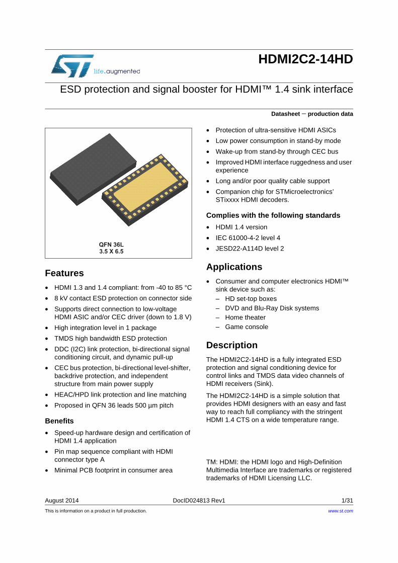
QFN 36L3.5 X 6.5
www.st.com

Contents HDMI2C2-14HD
2/31 DocID024813 Rev1
Contents
1 Functional description . . . . . . . . . . . . . . . . . . . . . . . . . . . . . . . . . . . . . . . 3
2 Application information . . . . . . . . . . . . . . . . . . . . . . . . . . . . . . . . . . . . . . 5
2.1 CEC line description . . . . . . . . . . . . . . . . . . . . . . . . . . . . . . . . . . . . . . . . . . 5
2.2 DDC functional block description . . . . . . . . . . . . . . . . . . . . . . . . . . . . . . . . 6
2.3 HEAC link and HPD line protection . . . . . . . . . . . . . . . . . . . . . . . . . . . . . . 9
2.4 TMDS channels ESD protection . . . . . . . . . . . . . . . . . . . . . . . . . . . . . . . . 10
2.5 Application block diagrams . . . . . . . . . . . . . . . . . . . . . . . . . . . . . . . . . . . . 10
3 Electrical characteristics . . . . . . . . . . . . . . . . . . . . . . . . . . . . . . . . . . . . 15
4 Package information . . . . . . . . . . . . . . . . . . . . . . . . . . . . . . . . . . . . . . . . 24
5 Recommendation on PCB assembly . . . . . . . . . . . . . . . . . . . . . . . . . . . 27
5.1 Stencil opening design . . . . . . . . . . . . . . . . . . . . . . . . . . . . . . . . . . . . . . . 27
5.2 Solder paste . . . . . . . . . . . . . . . . . . . . . . . . . . . . . . . . . . . . . . . . . . . . . . . 28
5.3 Placement . . . . . . . . . . . . . . . . . . . . . . . . . . . . . . . . . . . . . . . . . . . . . . . . 29
5.4 PCB design preference . . . . . . . . . . . . . . . . . . . . . . . . . . . . . . . . . . . . . . 29
5.5 Reflow profile . . . . . . . . . . . . . . . . . . . . . . . . . . . . . . . . . . . . . . . . . . . . . . 29
6 Ordering information . . . . . . . . . . . . . . . . . . . . . . . . . . . . . . . . . . . . . . . 30
7 Revision history . . . . . . . . . . . . . . . . . . . . . . . . . . . . . . . . . . . . . . . . . . . 30

DocID024813 Rev1 3/31
HDMI2C2-14HD Functional description
31
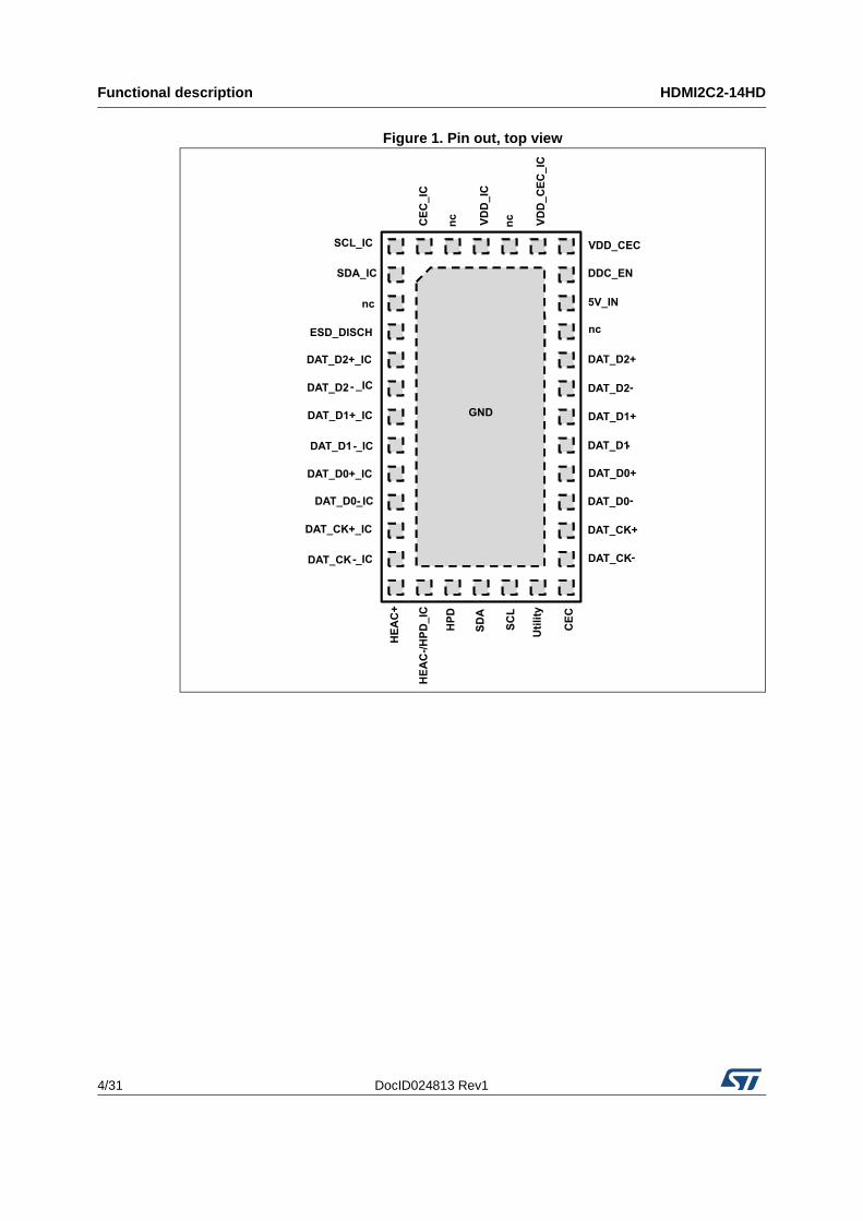
1 Functional description
The HDMI2C2-14HD is a fully integrated ESD protection and signal conditioning device for control links and TMDS data video channels of HDMI receiver (Sink).
The control stage provides a bidirectional buffer, integrating signal conditioning and dynamic pull-up on DDC bus for maximum system robustness and signal integrity. The HEAC (HDMI Ethernet and Audio return Channels) function is supported, making the component fully compliant with HDMI 1.4 version. A bidirectional CEC block is integrated, able to wake-up the application from stand-by mode (all power supply off, except the CEC power supply). The integrated TMDS links ESD protection allows a video data rate up to 10.2 Gbps, corresponding to the maximal speed specified by HDMI standard. All video format specified by HDMI standard (from 720p30 up to 1080p60 3D) are supported, giving maximum flexibility to designer. All these features are provided in a single 36 leads QFN package featuring natural PCB routing and saving space on the board.
The HDMI2C2-14HD is a simple solution that provides HDMI™ designers with an easy and fast way to reach full compliancy with the stringent HDMI 1.4 CTS on a wide temperature range. STMicroelectronics proposes a dual version dedicated for the Sources interfaces: the HDMI2C1-14HD.
Functional description HDMI2C2-14HD
4/31 DocID024813 Rev1
Figure 1. Pin out, top view
CE
C_
IC
HE
AC
+
VD
D_
IC
HP
D
HE
AC
-/H
PD
_IC
nc
nc
SD
A
Uti
lity
VD
D_
CE
C_
IC
SC
L
CE
C
DDC_EN
5V_IN
nc
DAT_D2+
DAT_D2-
DAT_D1+
DAT_D1-
DAT_D0+
DAT_D0-
DAT_CK+
DAT_CK-
SDA_IC
nc
ESD_DISCH
DAT_D2+_IC
DAT_D2- _IC
DAT_D1+_IC
DAT_D1-_IC
DAT_D0+_IC
DAT_D0-_IC
DAT_CK+_IC
DAT_CK-_IC
SCL_IC VDD_CEC
GND
DocID024813 Rev1 5/31
HDMI2C2-14HD Application information
31
2 Application information
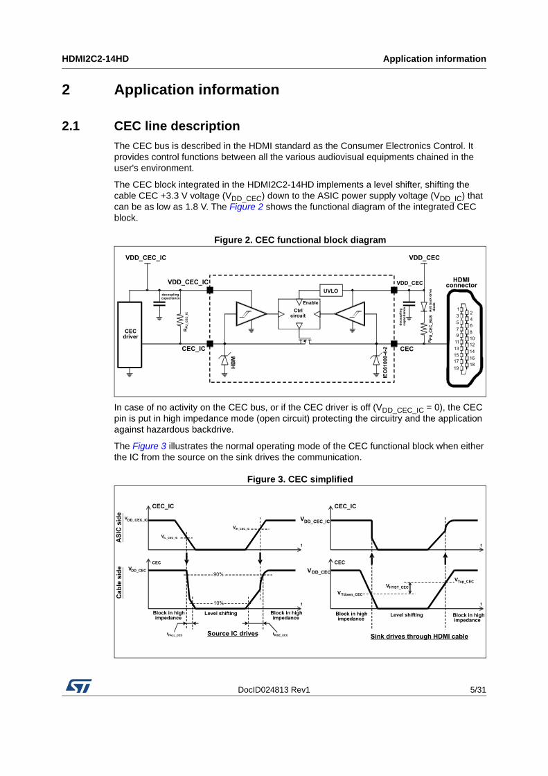
2.1 CEC line descriptionThe CEC bus is described in the HDMI standard as the Consumer Electronics Control. It provides control functions between all the various audiovisual equipments chained in the user's environment.
The CEC block integrated in the HDMI2C2-14HD implements a level shifter, shifting the cable CEC +3.3 V voltage (VDD_CEC) down to the ASIC power supply voltage (VDD_IC) that can be as low as 1.8 V. The Figure 2 shows the functional diagram of the integrated CEC block.
Figure 2. CEC functional block diagram
In case of no activity on the CEC bus, or if the CEC driver is off (VDD_CEC_IC = 0), the CEC pin is put in high impedance mode (open circuit) protecting the circuitry and the application against hazardous backdrive.
The Figure 3 illustrates the normal operating mode of the CEC functional block when either the IC from the source on the sink drives the communication.
Figure 3. CEC simplified
CEC_IC
VDD_CEC_IC
CEC
VDD_CECVDD_CEC_IC
VDD_CEC
CECdriver
UVLO
Ctrlcircuit
Enable
1
3
5
7
9
1112
1314
1516
1718
19
2
4
6
8
10
HDMIconnector
decoupling
deco
up
lin
g
capacitance
cap
acit
an
ce
RP
U_C
EC
_IC
HB
M
IEC
61
00
0-4
-2
RP
U_C
EC
_B
US
An
ti b
ac
k d
riv
ed
iod
e
Cab
le s
ide
AS
IC s
ide
VDD_CEC_IC
CEC_IC
VDD_CEC
CEC
VTdown_CEC
VTup_CEC
VHYST_CEC
VDD_CEC_IC
CEC_IC
VDD_CEC
CEC
VIL_CEC_IC
VIH_CEC_IC
Block in highimpedance
Level shifting
Source IC drives Sink drives through HDMI cable
Block in highimpedance
Block in highimpedance
Level shifting Block in highimpedance
t
t
t
t10%
90%
tFALL_CEC tRISE_CEC
Application information HDMI2C2-14HD
6/31 DocID024813 Rev1
In case the application is set in stand-by mode, the +5 V main supply of the application is generally powered off in order to reduce as much as possible the global power consumption. The CEC driver can be the only device still working in low power mode, allowing a wake up of the whole application through the CEC line. When the main power supply +5 V is switched off, and if the CEC bus is still active (VDD_CEC power in on state), the HDMI2C2-14HD keeps the CEC bus working properly while all other outputs of the component are put in high impedance mode.
The CEC output (cable side) integrates a protection against ESD which is compliant with IEC61000-4-2 standard, level 4 (8kV contact).
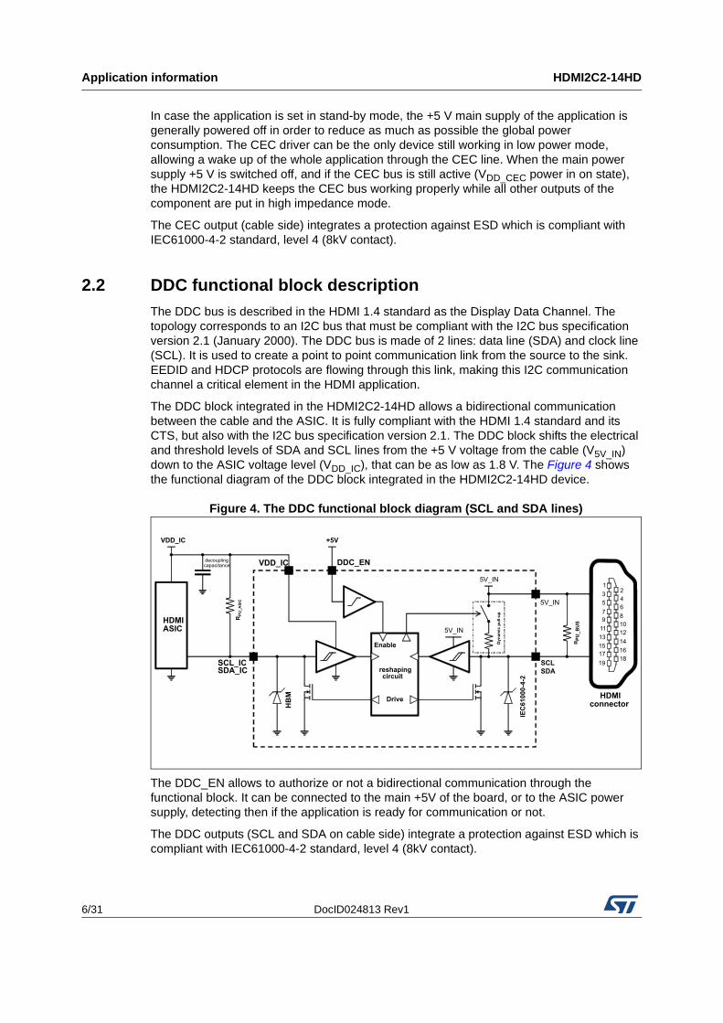
2.2 DDC functional block descriptionThe DDC bus is described in the HDMI 1.4 standard as the Display Data Channel. The topology corresponds to an I2C bus that must be compliant with the I2C bus specification version 2.1 (January 2000). The DDC bus is made of 2 lines: data line (SDA) and clock line (SCL). It is used to create a point to point communication link from the source to the sink. EEDID and HDCP protocols are flowing through this link, making this I2C communication channel a critical element in the HDMI application.
The DDC block integrated in the HDMI2C2-14HD allows a bidirectional communication between the cable and the ASIC. It is fully compliant with the HDMI 1.4 standard and its CTS, but also with the I2C bus specification version 2.1. The DDC block shifts the electrical and threshold levels of SDA and SCL lines from the +5 V voltage from the cable (V5V_IN) down to the ASIC voltage level (VDD_IC), that can be as low as 1.8 V. The Figure 4 shows the functional diagram of the DDC block integrated in the HDMI2C2-14HD device.
Figure 4. The DDC functional block diagram (SCL and SDA lines)
The DDC_EN allows to authorize or not a bidirectional communication through the functional block. It can be connected to the main +5V of the board, or to the ASIC power supply, detecting then if the application is ready for communication or not.
The DDC outputs (SCL and SDA on cable side) integrate a protection against ESD which is compliant with IEC61000-4-2 standard, level 4 (8kV contact).
SCL_ICSDA_IC
VDD_IC
reshapingcircuit
5V_IN
5V_IN
SCL
SDA
VDD_IC
HDMIASIC
+5V
DDC_EN
5V_IN
Enable
Drive HDMIconnector
decouplingcapacitance
RP
U_A
SIC
HB
M
IEC
61
00
0-4
-2
RP
U_B
US
Dyn
am
ic p
ull-u
p
12
14
16
18
2
4
6
8
10
1
3
5
7
9
11
13
15
17
19
DocID024813 Rev1 7/31
HDMI2C2-14HD Application information
31
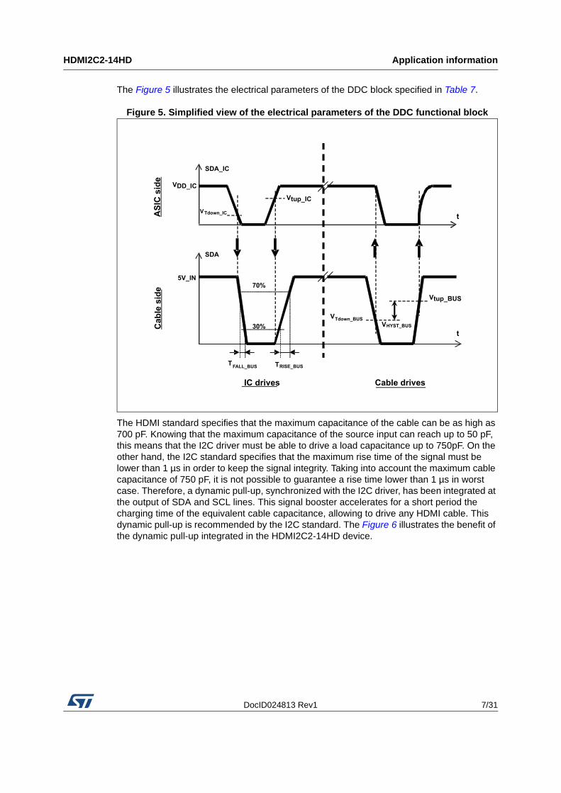
The Figure 5 illustrates the electrical parameters of the DDC block specified in Table 7.
Figure 5. Simplified view of the electrical parameters of the DDC functional block
The HDMI standard specifies that the maximum capacitance of the cable can be as high as 700 pF. Knowing that the maximum capacitance of the source input can reach up to 50 pF, this means that the I2C driver must be able to drive a load capacitance up to 750pF. On the other hand, the I2C standard specifies that the maximum rise time of the signal must be lower than 1 µs in order to keep the signal integrity. Taking into account the maximum cable capacitance of 750 pF, it is not possible to guarantee a rise time lower than 1 µs in worst case. Therefore, a dynamic pull-up, synchronized with the I2C driver, has been integrated at the output of SDA and SCL lines. This signal booster accelerates for a short period the charging time of the equivalent cable capacitance, allowing to drive any HDMI cable. This dynamic pull-up is recommended by the I2C standard. The Figure 6 illustrates the benefit of the dynamic pull-up integrated in the HDMI2C2-14HD device.
5V_IN
SDA
VDD_IC
SDA_IC
VTdown_IC
TRISE_BUS
Vtup_IC
70%
30%
VTdown_BUS
Vtup_BUS
VHYST_BUS
IC drives
AS
IC s
ide
Ca
ble
sid
e
Cable drives
TFALL_BUS
t
t
Application information HDMI2C2-14HD
8/31 DocID024813 Rev1
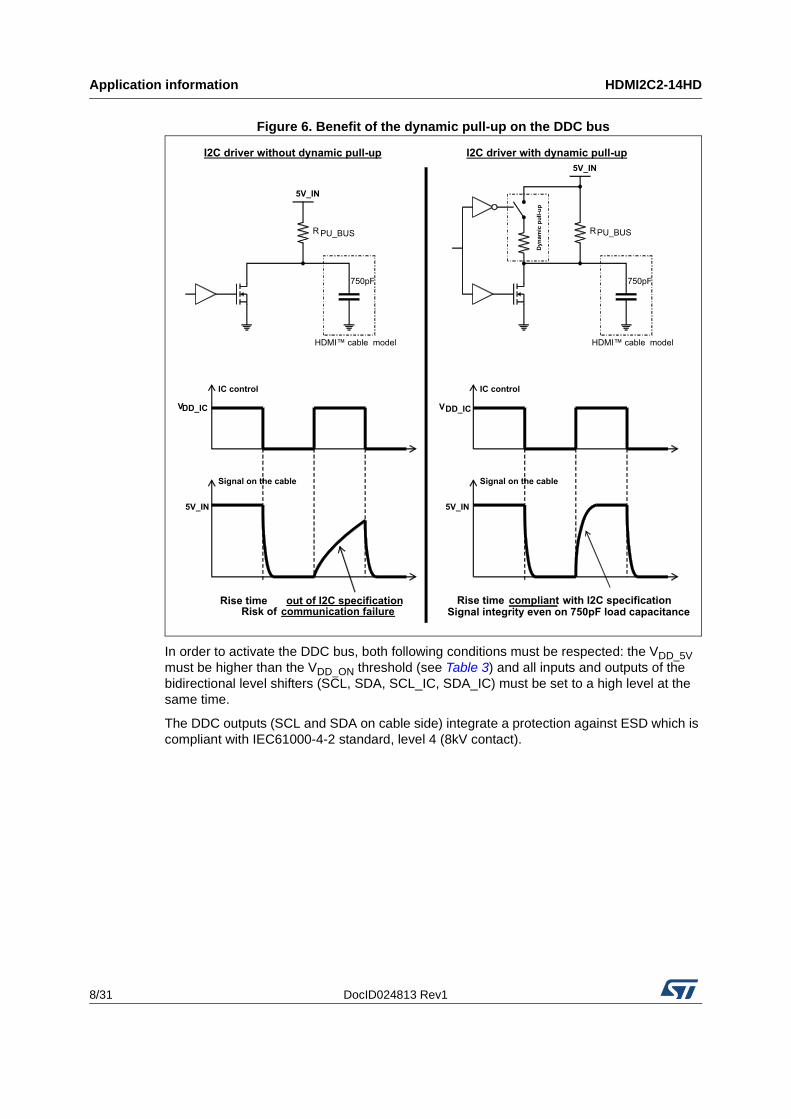
Figure 6. Benefit of the dynamic pull-up on the DDC bus
In order to activate the DDC bus, both following conditions must be respected: the VDD_5V must be higher than the VDD_ON threshold (see Table 3) and all inputs and outputs of the bidirectional level shifters (SCL, SDA, SCL_IC, SDA_IC) must be set to a high level at the same time.
The DDC outputs (SCL and SDA on cable side) integrate a protection against ESD which is compliant with IEC61000-4-2 standard, level 4 (8kV contact).
Rise time out of I2C specificationRisk of communication failure
I2C driver without dynamic pull-up I2C driver with dynamic pull-up
Signal on the cable
IC control
5V_IN
VDD_IC
IC control
Signal on the cable
5V_IN
VDD_IC
RPU_BUS
5V_IN
HDMI™ cable model
750pF
R PU_BUS
5V_IN
HDMI™ cable model
750pF
Rise time compliant with I2C specificationSignal integrity even on 750pF load capacitance
Dyn
am
ic p
ull-u
p
DocID024813 Rev1 9/31
HDMI2C2-14HD Application information
31
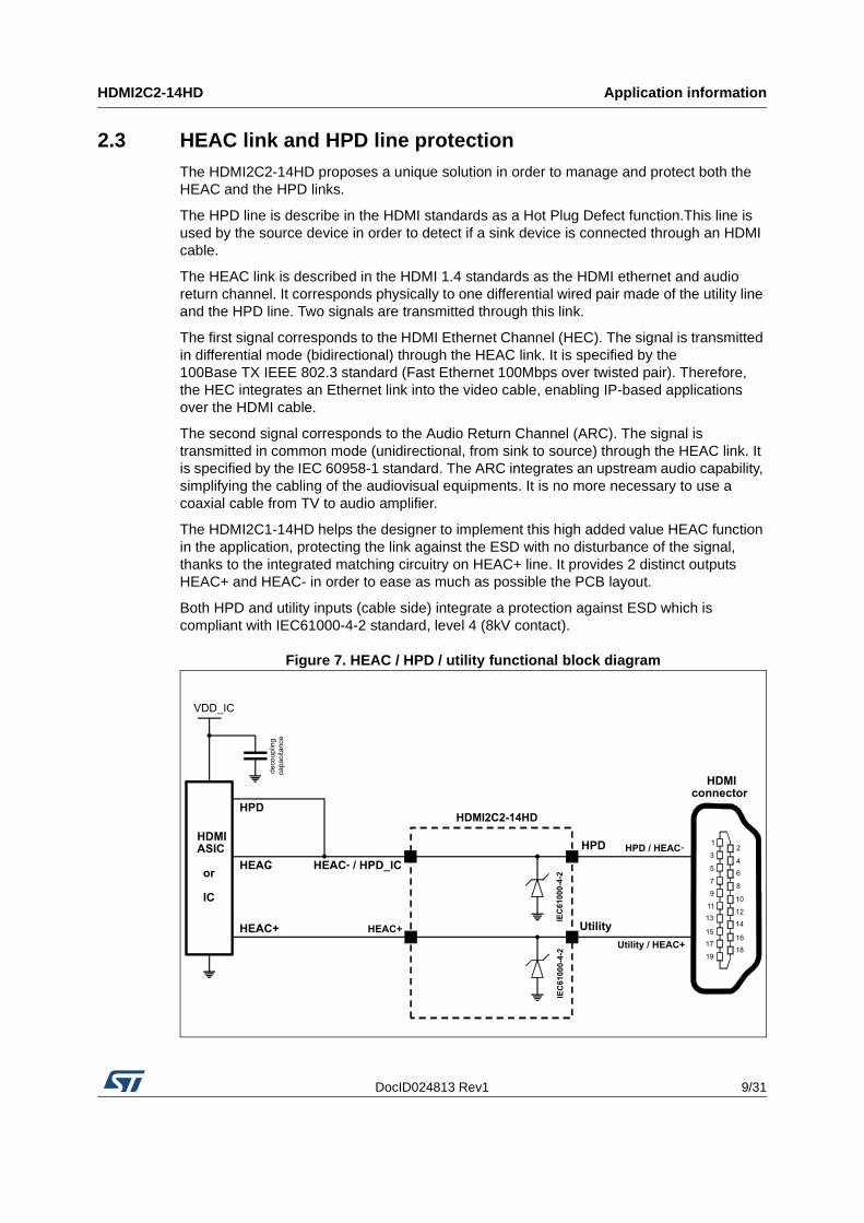
2.3 HEAC link and HPD line protectionThe HDMI2C2-14HD proposes a unique solution in order to manage and protect both the HEAC and the HPD links.
The HPD line is describe in the HDMI standards as a Hot Plug Defect function.This line is used by the source device in order to detect if a sink device is connected through an HDMI cable.
The HEAC link is described in the HDMI 1.4 standards as the HDMI ethernet and audio return channel. It corresponds physically to one differential wired pair made of the utility line and the HPD line. Two signals are transmitted through this link.
The first signal corresponds to the HDMI Ethernet Channel (HEC). The signal is transmitted in differential mode (bidirectional) through the HEAC link. It is specified by the 100Base TX IEEE 802.3 standard (Fast Ethernet 100Mbps over twisted pair). Therefore, the HEC integrates an Ethernet link into the video cable, enabling IP-based applications over the HDMI cable.
The second signal corresponds to the Audio Return Channel (ARC). The signal is transmitted in common mode (unidirectional, from sink to source) through the HEAC link. It is specified by the IEC 60958-1 standard. The ARC integrates an upstream audio capability, simplifying the cabling of the audiovisual equipments. It is no more necessary to use a coaxial cable from TV to audio amplifier.
The HDMI2C1-14HD helps the designer to implement this high added value HEAC function in the application, protecting the link against the ESD with no disturbance of the signal, thanks to the integrated matching circuitry on HEAC+ line. It provides 2 distinct outputs HEAC+ and HEAC- in order to ease as much as possible the PCB layout.
Both HPD and utility inputs (cable side) integrate a protection against ESD which is compliant with IEC61000-4-2 standard, level 4 (8kV contact).
Figure 7. HEAC / HPD / utility functional block diagram
HPD
HEAC- / HPD_IC
Utility
HDMIASIC
or
IC
VDD_IC
Utility / HEAC+
HPD / HEAC-
HEAC+
HPD
1
3
5
7
9
2
4
6
8
HDMIconnector
HEAC-
HEAC+
HDMI2C2-14HD
1011
15
13
19
17
12
16
14
18
IEC
61
00
0-4
-2IE
C6
10
00
-4-2
de
co
up
ling
ca
pa
cita
nce
Application information HDMI2C2-14HD
10/31 DocID024813 Rev1
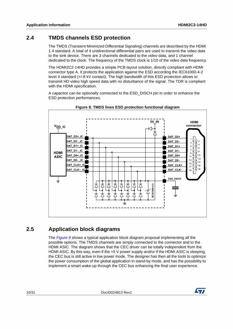
2.4 TMDS channels ESD protectionThe TMDS (Transient Minimized Differential Signaling) channels are described by the HDMI 1.4 standard. A total of 4 unidirectional differential pairs are used to transmit the video data to the sink device. There are 3 channels dedicated to the video data, and 1 channel dedicated to the clock. The frequency of the TMDS clock is 1/10 of the video data frequency.
The HDMI2C2-14HD provides a simple PCB layout solution, directly compliant with HDMI connector type A. It protects the application against the ESD according the IEC61000-4-2 level 4 standard (+/-8 kV contact). The high bandwidth of this ESD protection allows to transmit HD video high speed data with no disturbance of the signal. The TDR is compliant with the HDMI specification.
A capacitor can be optionally connected to the ESD_DISCH pin in order to enhance the ESD protection performances.
Figure 8. TMDS lines ESD protection functional diagram
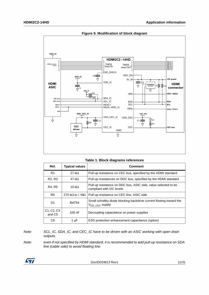
2.5 Application block diagramsThe Figure 9 shows a typical application block diagram proposal implementing all the possible options. The TMDS channels are simply connected to the connector and to the HDMI ASIC. The diagram shows that the CEC driver can be totally independent from the HDMI ASIC. By this way, even if the +5 V power supply and/or if the HDMI ASIC is sleeping, the CEC bus is still active in low power mode. The designer has then all the tools to optimize the power consumption of the global application in stand-by mode, and has the possibility to implement a smart wake-up through the CEC bus enhancing the final user experience.
DAT_D2+
DAT_D2-
DAT_D1+
DAT_D1-
DAT_D0+
DAT_D0 -
DAT_CLK-
5V_IN
DAT_CLK+
ESD_DSICH
HDMIASIC
DAT_D2+_IC
DAT_D2 -_IC
DAT_D1+_IC
DAT_D1-_IC
DAT_D0+_IC
DAT_D0 - _IC
DAT_CLK-_IC
DAT_CLK+_IC
HDMIconnectorVDD_IC
IEC
61000-4
-2
1
3
5
7
9
11
13
15
17
19
12
14
16
18
2
4
6
8
10
DocID024813 Rev1 11/31
HDMI2C2-14HD Application information
31
Figure 9. Modification of block diagram
Note: SCL_IC, SDA_IC, and CEC_IC have to be driven with an ASIC working with open drain outputs.
Note: even if not specified by HDMI standard, it is recommended to add pull-up resistance on SDA line (cable side) to avoid floating line.
Table 1. Block diagrams references
Ref. Typical values Comment
R1 27 kΩ Pull-up resistance on CEC bus, specified by the HDMI standard
R2, R3 47 kΩ Pull-up resistances on DDC bus, specified by the HDMI standard
R4, R5 10 kΩ Pull-up resistance on DDC bus, ASIC side, value selected to be compliant with I2C levels
R6 270 kΩ to 1 ΜΩ Pull-up resistance on CEC line, ASIC side
D1 BAT54Small schottky diode blocking backdrive current flowing toward the VDD_CEC supply
C1, C2, C3 and C5
100 nF Decoupling capacitance on power supplies
C6 1 µF ESD protection enhancement capacitance (option)
CEC
driver
SCL_IC
SDA_IC
SDA
SCL
CEC bus
VDD_CEC_IC
VDD_IC
VDD_IC
VDD_CEC
DDC_EN
VDD_IC
VDD_CEC_IC
CEC_IC
5V_IN
HPD
SDA
SCL
CEC
VDD_CEC
Utility
ESD_DISCH
VDD_IC
4 TMDS channels
8 lines
HPD
DDC data
HPD / HEAC-
Utility / HEAC+
HEAC+HEAC- /HPD_IC
TMDSlines IN
TMDSlines OUT
HEAC+
HEAC -
HDMI2C2
HDMIASIC
HDMIconnector
-14HDTMDS data 2+
TMDS data 2-TMDS data 1+TMDS data 1-TMDS data 0+TMDS data 0-TMDS Clock+TMDS Clock-
+5V power
C6
C3
R2R3
C2
R1
D1C1C5R6
R4
R5
DDC clock
GND
EEPROM(EEDID)
Application information HDMI2C2-14HD
12/31 DocID024813 Rev1
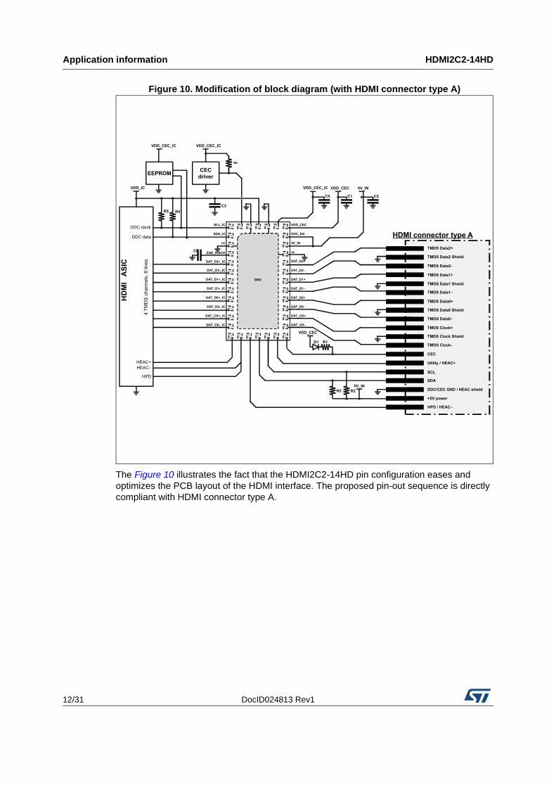
Figure 10. Modification of block diagram (with HDMI connector type A)
The Figure 10 illustrates the fact that the HDMI2C2-14HD pin configuration eases and optimizes the PCB layout of the HDMI interface. The proposed pin-out sequence is directly compliant with HDMI connector type A.
C3
HDMI connector type A
VDD_CEC
HEAC+
HEAC-
5V_IN
CEC
driver
VDD_IC
VDD_CEC_IC
VDD_CECVDD_CEC_IC
DDC clock
DDC data
5V_IN
4T
MD
S c
ha
nn
els
, 8
lin
es
HD
MI
AS
IC
D1 R1
R2R3
C2C1C5
C6
R4R5
R6
TMDS Data2+
TMDS Data2 Shield
TMDS Data2-
TMDS Data1+
TMDS Data1 Shield
TMDS Data1-
TMDS Data0+
TMDS Data0 Shield
TMDS Data0-
TMDS Clock+
TMDS Clock Shield
TMDS Clock-
CEC
Utility / HEAC+
SCL
SDA
DDC/CEC GND / HEAC shield
+5V power
HPD / HEAC-
VDD_CEC_IC
EEPROM
HPD
DDC_EN
5V_IN
nc
DAT_D2+
DAT_D2-
DAT_D1+
DAT_D1-
DAT_D0+
DAT_D0-
DAT_CK+
DAT_CK-
SDA_IC
nc
ESD_DISCH
DAT_D2+_IC
DAT_D2-_IC
DAT_D1+_IC
DAT_D1-_IC
DAT_D0+_IC
DAT_D0-_IC
DAT_CK+_IC
DAT_CK-_IC
SCL_IC VDD_CEC
GND
DocID024813 Rev1 13/31
HDMI2C2-14HD Application information
31
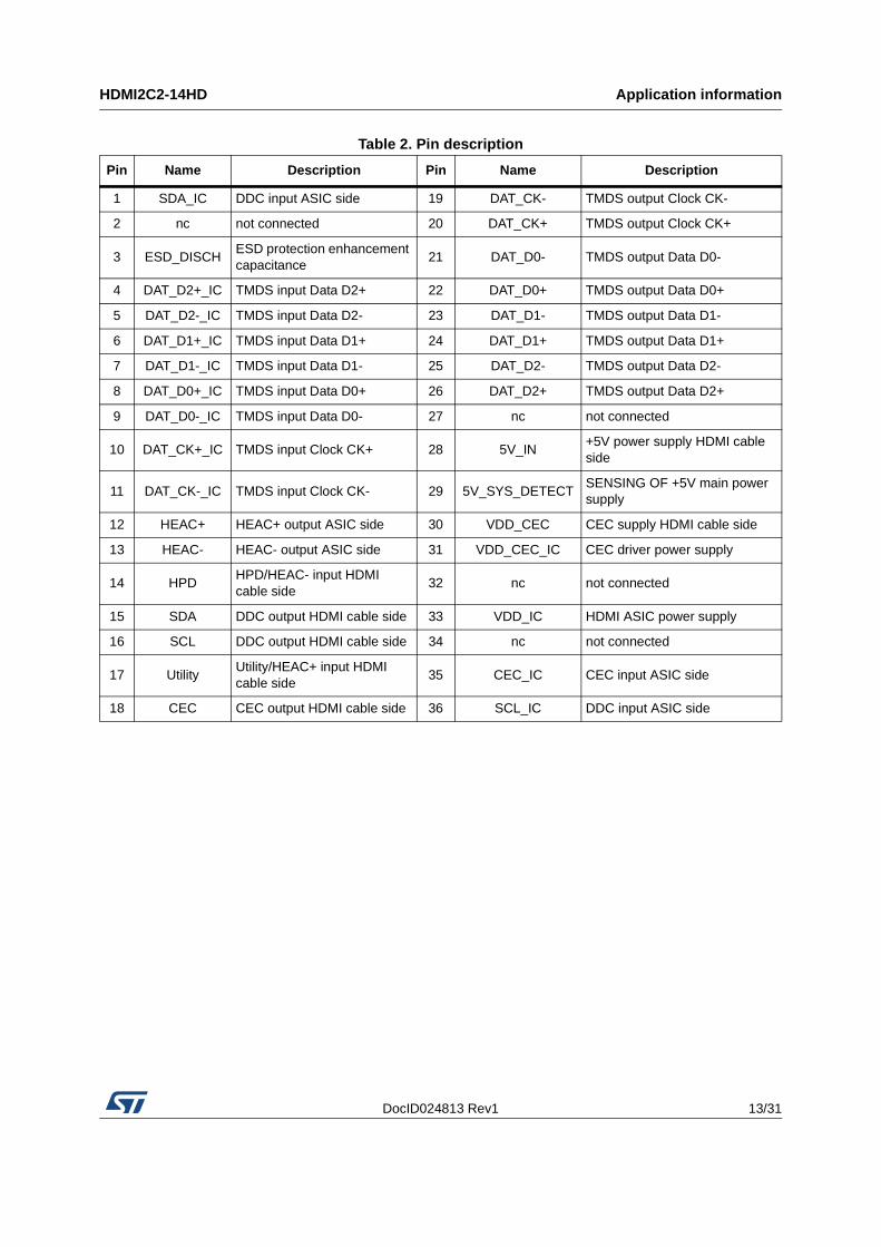
Table 2. Pin description
Pin Name Description Pin Name Description
1 SDA_IC DDC input ASIC side 19 DAT_CK- TMDS output Clock CK-
2 nc not connected 20 DAT_CK+ TMDS output Clock CK+
3 ESD_DISCHESD protection enhancement capacitance
21 DAT_D0- TMDS output Data D0-
4 DAT_D2+_IC TMDS input Data D2+ 22 DAT_D0+ TMDS output Data D0+
5 DAT_D2-_IC TMDS input Data D2- 23 DAT_D1- TMDS output Data D1-
6 DAT_D1+_IC TMDS input Data D1+ 24 DAT_D1+ TMDS output Data D1+
7 DAT_D1-_IC TMDS input Data D1- 25 DAT_D2- TMDS output Data D2-
8 DAT_D0+_IC TMDS input Data D0+ 26 DAT_D2+ TMDS output Data D2+
9 DAT_D0-_IC TMDS input Data D0- 27 nc not connected
10 DAT_CK+_IC TMDS input Clock CK+ 28 5V_IN+5V power supply HDMI cable side
11 DAT_CK-_IC TMDS input Clock CK- 29 5V_SYS_DETECTSENSING OF +5V main power supply
12 HEAC+ HEAC+ output ASIC side 30 VDD_CEC CEC supply HDMI cable side
13 HEAC- HEAC- output ASIC side 31 VDD_CEC_IC CEC driver power supply
14 HPDHPD/HEAC- input HDMI cable side
32 nc not connected
15 SDA DDC output HDMI cable side 33 VDD_IC HDMI ASIC power supply
16 SCL DDC output HDMI cable side 34 nc not connected
17 UtilityUtility/HEAC+ input HDMI cable side
35 CEC_IC CEC input ASIC side
18 CEC CEC output HDMI cable side 36 SCL_IC DDC input ASIC side
Application information HDMI2C2-14HD
14/31 DocID024813 Rev1
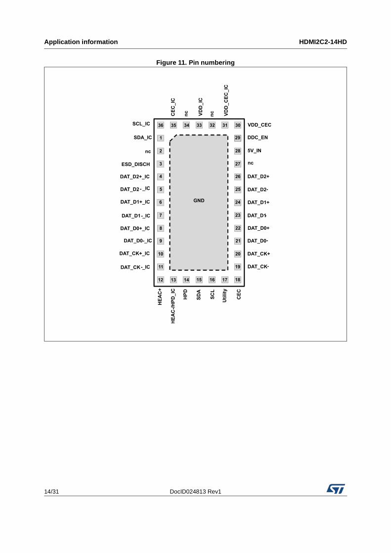
Figure 11. Pin numbering
CE
C_
IC
HE
AC
+
VD
D_
IC
HP
D
HE
AC
-/H
PD
_IC
nc
nc
SD
A
Uti
lity
VD
D_
CE
C_
IC
SC
L
CE
C
DDC_EN
5V_IN
nc
DAT_D2+
DAT_D2-
DAT_D1+
DAT_D1-
DAT_D0+
DAT_D0-
DAT_CK+
DAT_CK-
SDA_IC
nc
ESD_DISCH
DAT_D2+_IC
DAT_D2- _IC
DAT_D1+_IC
DAT_D1-_IC
DAT_D0+_IC
DAT_D0-_IC
DAT_CK+_IC
DAT_CK-_IC
SCL_IC VDD_CEC
GND
313233343536
1
2
3
4
5
6
7
8
9
10
11
12 13
30
29
28
27
26
25
24
23
22
21
20
19
1817161514
DocID024813 Rev1 15/31
HDMI2C2-14HD Electrical characteristics
31
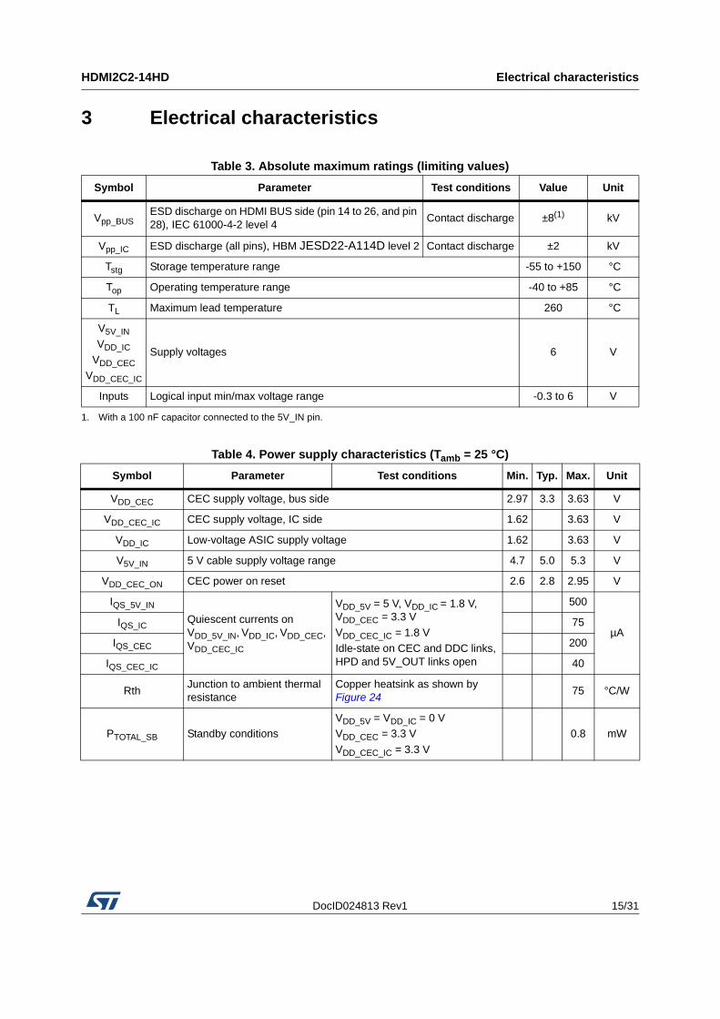
3 Electrical characteristics
Table 3. Absolute maximum ratings (limiting values)
Symbol Parameter Test conditions Value Unit
Vpp_BUSESD discharge on HDMI BUS side (pin 14 to 26, and pin 28), IEC 61000-4-2 level 4
Contact discharge ±8(1) kV
Vpp_IC ESD discharge (all pins), HBM JESD22-A114D level 2 Contact discharge ±2 kV
Tstg Storage temperature range -55 to +150 °C
Top Operating temperature range -40 to +85 °C
TL Maximum lead temperature 260 °C
V5V_IN
VDD_IC
VDD_CEC
VDD_CEC_IC
Supply voltages 6 V
Inputs Logical input min/max voltage range -0.3 to 6 V
1. With a 100 nF capacitor connected to the 5V_IN pin.
Table 4. Power supply characteristics (Tamb = 25 °C)
Symbol Parameter Test conditions Min. Typ. Max. Unit
VDD_CEC CEC supply voltage, bus side 2.97 3.3 3.63 V
VDD_CEC_IC CEC supply voltage, IC side 1.62 3.63 V
VDD_IC Low-voltage ASIC supply voltage 1.62 3.63 V
V5V_IN 5 V cable supply voltage range 4.7 5.0 5.3 V
VDD_CEC_ON CEC power on reset 2.6 2.8 2.95 V
IQS_5V_IN
Quiescent currents on VDD_5V_IN, VDD_IC, VDD_CEC, VDD_CEC_IC
VDD_5V = 5 V, VDD_IC = 1.8 V, VDD_CEC = 3.3 V
VDD_CEC_IC = 1.8 VIdle-state on CEC and DDC links, HPD and 5V_OUT links open
500
µAIQS_IC 75
IQS_CEC 200
IQS_CEC_IC 40
RthJunction to ambient thermal resistance
Copper heatsink as shown by Figure 24
75 °C/W
PTOTAL_SB Standby conditionsVDD_5V = VDD_IC = 0 VVDD_CEC = 3.3 V
VDD_CEC_IC = 3.3 V
0.8 mW
Electrical characteristics HDMI2C2-14HD
16/31 DocID024813 Rev1
Table 5. CEC electrical characteristics(1)
Symbol Parameter Test conditions Min. Typ. Max. Unit
VTup_CEC Upward input voltage threshold on bus side 1.6 V
VTdown_CEC Downward input voltage threshold on bus side 0.8 V
VHYST_CEC Input hysteresis on bus side 0.4 V
TRISE_CEC Output rise-time (10% to 90%) RUP = 14.1 kΩ(2) ±5%
CCEC CABLE = 9.7 nF
250 µs
TFALL_CEC Output fall-time (90% to 10%) 50 µs
IOFF_CECLeakage current in powered-off state VDD_5V = 0 V, VDD_IC = 0 V,
VDD_CEC = 3.3 V1.8 µA
VIL_CEC_IC Input low level on IC side 0.5 %VDD_IC
VIH_CEC_IC Input high level on IC side 70 %VDD_IC
RON_CECOn resistance across CEC and CEC_IC pins
CEC pin to 0 V 115 160 Ω
CIN_CEC Input capacitance on CEC link
VDD_5V = 0 VVDD_CEC = 0 V
VDD_IC = 0 VVBIAS = 0 V, f = 1 MHz,VOSC = 30 mV
40(3) pF
1. Tamb = 25 °C, VDD_CEC = 3.3 V, VDD_CEC_IC = 1.8 V, unless otherwise specified
2. Test conditions are compliant with worst case CEC specification:
- Correspond to two 27 kΩ +5% pull-up resistances in parallel (compliant with HDMI CTS)
- Max capacitance corresponding to 9 equipment chained on the CEC bus
3. Maximum capacitance allowed at connector output is 200 pF in HDMI 1.4 specification
Table 6. HPD, HEAC, and utility line electrical characteristics(1)
Symbol Parameter Test conditionsValue
UnitMin. Typ. Max.
CIN_HPDCIN_UTILITY
Input capacitanceVDD_5V = 0 V, VBIAS = 0 V
f = 100 kHz, VOSC = 30 mV9 pF
fCUT_HEAC Cut-off frequency of HEAC bus 500 MHz
1. Tamb = 25°C, VDD_5V = 5 V, unless otherwise specified.
DocID024813 Rev1 17/31
HDMI2C2-14HD Electrical characteristics
31
Table 7. DDC bus (SDA and SCL lines) electrical characteristics(1)
Symbol Parameter Test conditionsValue
UnitMin. Typ. Max.
VTup_BUS Upward input voltage threshold on bus side 3.5 V
VTdown_BUS Downward input voltage threshold on bus side 1.5 V
VHYST_BUS Input hysteresis on bus side 1.0 1.3 V
VOL_BUS Output low levelCurrent sunk by SDA and SCL pin is 3 mA
0.35 V
TRISE_BUS Output rise-time (30% to 70%)CBUS = 750 pF(2)
RUP = 2 KΩ //47 KΩ + 10%(3) 500 ns
TFALL_BUS Output fall-time (30% to 70%) 50 ns
VTup_IC Upward input voltage threshold on IC side 55 60 65 %VDD_IC
VTdown_IC Downward input voltage thresholds IC side 35 40 45 %VDD_IC
VOL_IC Output low level on IC sideCurrent sunk by SDA_IC or SCL_IC pins is 500 µA
20 mV
CIN_DDC Input capacitance on DDC link
VDD_5V = 0 VVDD_IC = 0 VVDD_CEC = 0 VVBIAS = 0 V, f = 1 MHzVOSC = 30 mV
9 17(4) pF
VEN_DCC(5) DCC enabling 4.1 V
1. Tamb = 25 °C, VDD_5V = 5 V, VDD_IC = 1.8 V, unless otherwise specified
2. Maximum load capacitance allowed on I2C entire link (cable + connector) is 750 pF in HDMI 1.4 specification.
3. Two pull-up resistors in parallel (sink 47 kΩ + source 2 kΩ).
4. Maximum capacitance allowed at connector output is 50 pF in HDMI 1.4 specification
5. In order to activate the DCC lines, the level on DCC_EN pin has to reach the VEN_DCC min value. The inputs and ouputs of the bidirectional level shifters must be set to a high level after the power-on, and the HPD line has to be activated one time.
Electrical characteristics HDMI2C2-14HD
18/31 DocID024813 Rev1
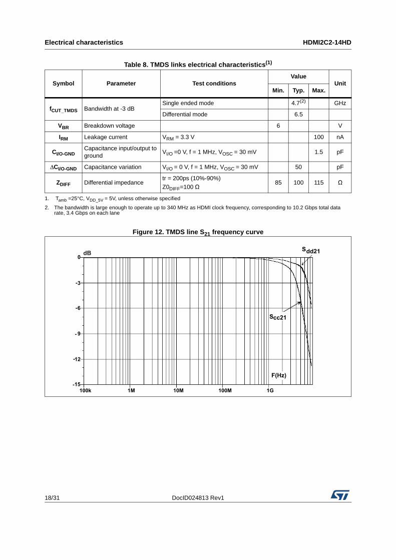
Figure 12. TMDS line S21 frequency curve
Table 8. TMDS links electrical characteristics(1)
Symbol Parameter Test conditionsValue
UnitMin. Typ. Max.
fCUT_TMDS Bandwidth at -3 dBSingle ended mode 4.7(2) GHz
Differential mode 6.5
VBR Breakdown voltage 6 V
IRM Leakage current VRM = 3.3 V 100 nA
CI/O-GNDCapacitance input/output to ground
VI/O =0 V, f = 1 MHz, VOSC = 30 mV 1.5 pF
ΔCI/O-GND Capacitance variation VI/O = 0 V, f = 1 MHz, VOSC = 30 mV 50 pF
ZDIFF Differential impedancetr = 200ps (10%-90%)
Z0DIFF=100 Ω85 100 115 Ω
1. Tamb =25°C, VDD_5V = 5V, unless otherwise specified
2. The bandwidth is large enough to operate up to 340 MHz as HDMI clock frequency, corresponding to 10.2 Gbps total data rate, 3.4 Gbps on each lane
Sdd21dB0
-3
-6
- 9
-12
-15100k 1M 10M 100M 1G
F(Hz)
Scc21
DocID024813 Rev1 19/31
HDMI2C2-14HD Electrical characteristics
31
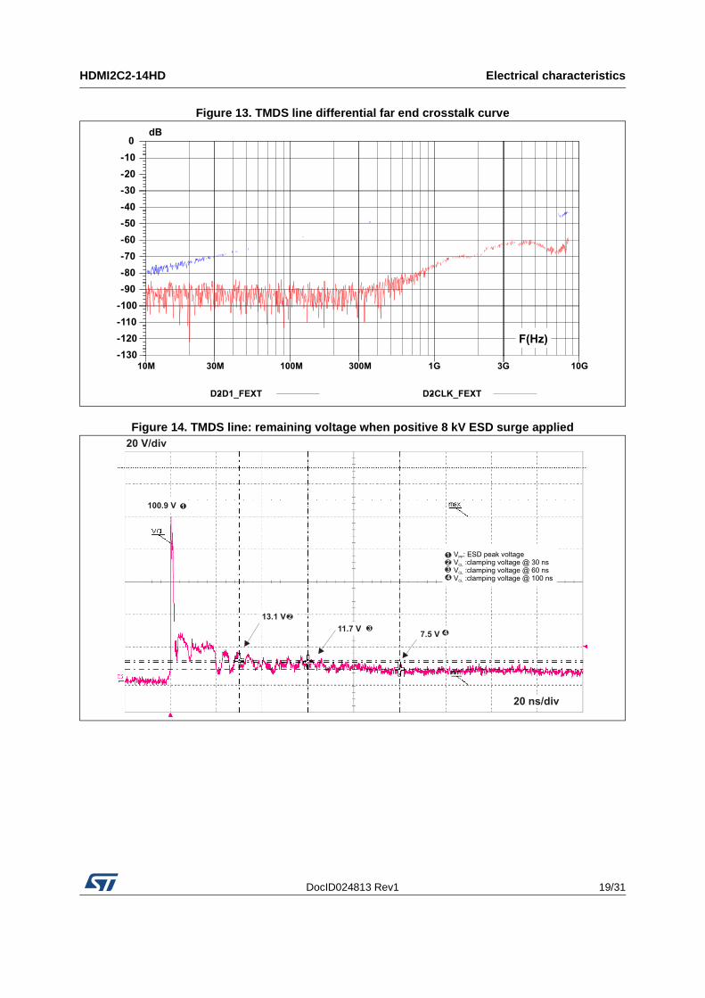
Figure 13. TMDS line differential far end crosstalk curve
Figure 14. TMDS line: remaining voltage when positive 8 kV ESD surge applied
10M 30M 100M 300M 1G 3G 10G
-130
-120
-110
-100
-90
-80
-70
-60
-50
-40
-30
-20
-10
0dB
D2-D1_FEXT D2-CLK_FEXT
F(Hz)
20 V/div
V : ESD peak voltagePP
V :clamping voltage @ 30 nsCL
V :clamping voltage @ 60 nsCL
V :clamping voltage @ 100 nsCL
123
4
20 ns/div
7.5 V 411.7 V 3
13.1 V 2
100.9 V 1
Electrical characteristics HDMI2C2-14HD
20/31 DocID024813 Rev1
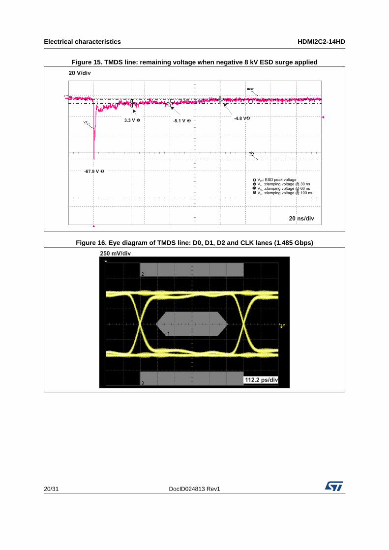
Figure 15. TMDS line: remaining voltage when negative 8 kV ESD surge applied
Figure 16. Eye diagram of TMDS line: D0, D1, D2 and CLK lanes (1.485 Gbps)
V : ESD peak voltagePP
V :clamping voltage @ 30 nsCL
V :clamping voltage @ 60 nsCL
V :clamping voltage @ 100 nsCL
123
4
20 V/div
20 ns/div
1-67.9 V
23.3 V 3-5.1 V4-4.8 V
250 mV/div
112.2 ps/div
DocID024813 Rev1 21/31
HDMI2C2-14HD Electrical characteristics
31
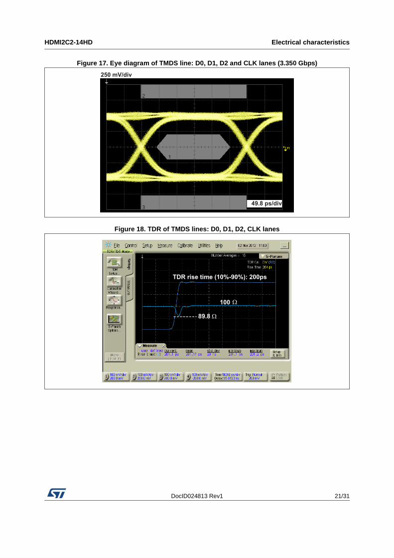
Figure 17. Eye diagram of TMDS line: D0, D1, D2 and CLK lanes (3.350 Gbps)
Figure 18. TDR of TMDS lines: D0, D1, D2, CLK lanes
250 mV/div
49.8 ps/div
TDR rise time (10%-90%): 200ps
100
89.8
Electrical characteristics HDMI2C2-14HD
22/31 DocID024813 Rev1
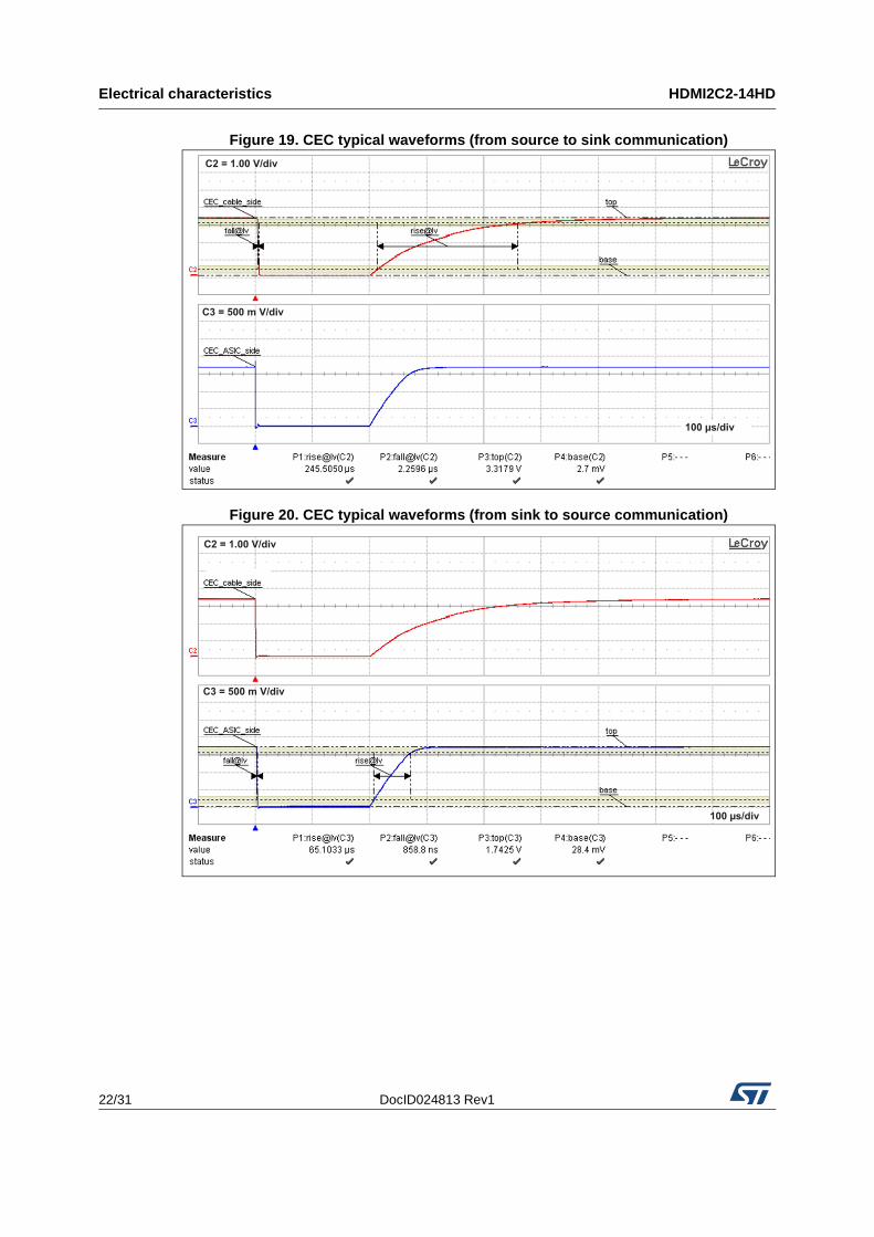
Figure 19. CEC typical waveforms (from source to sink communication)
Figure 20. CEC typical waveforms (from sink to source communication)
C2 = 1.00 V/div
C3 = 500 m V/div
100 µs/div
C2 = 1.00 V/div
C3 = 500 m V/div
100 µs/div
DocID024813 Rev1 23/31
HDMI2C2-14HD Electrical characteristics
31
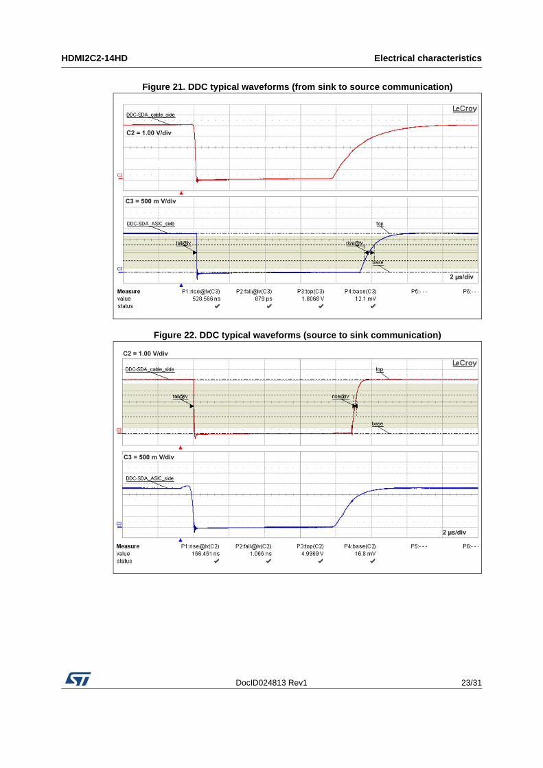
Figure 21. DDC typical waveforms (from sink to source communication)
Figure 22. DDC typical waveforms (source to sink communication)
2 µs/div
C3 = 500 m V/div
C2 = 1.00 V/div
C3 = 500 m V/div
C2 = 1.00 V/div
2 µs/div
Package information HDMI2C2-14HD
24/31 DocID024813 Rev1
4 Package information
• Epoxy meets UL94, V0
• Lead-free packages
In order to meet environmental requirements, ST offers these devices in different grades of ECOPACK® packages, depending on their level of environmental compliance. ECOPACK® specifications, grade definitions and product status are available at: www.st.com. ECOPACK® is an ST trademark.
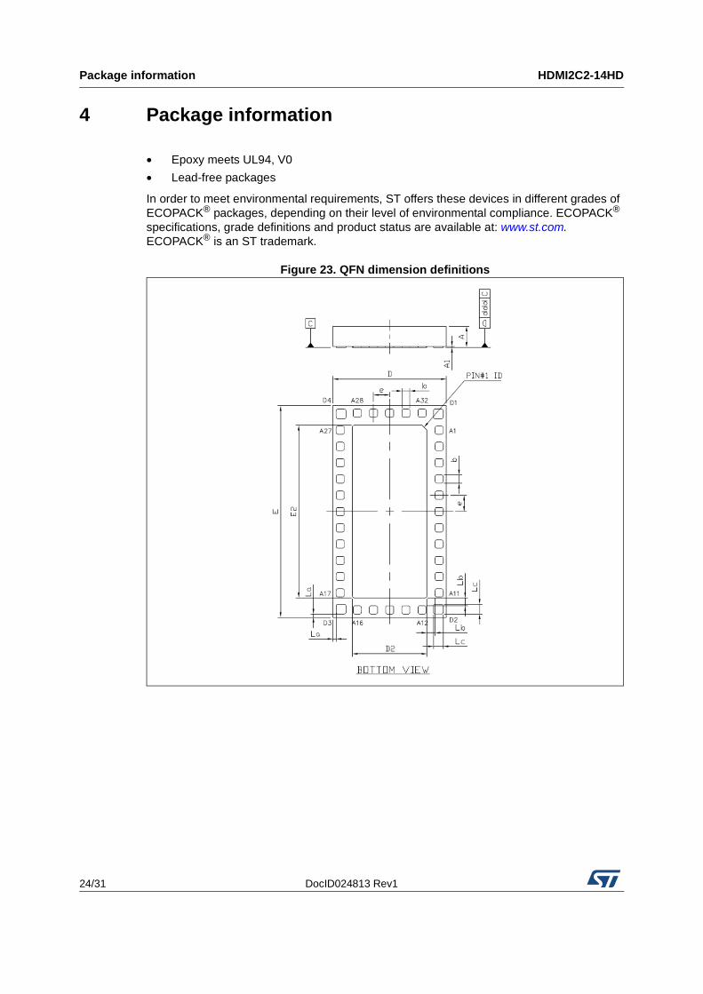
Figure 23. QFN dimension definitions
DocID024813 Rev1 25/31
HDMI2C2-14HD Package information
31
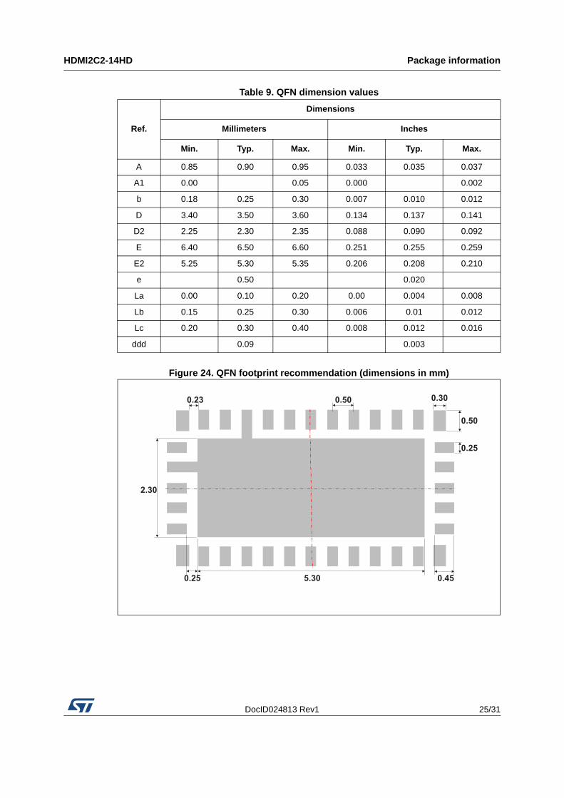
Figure 24. QFN footprint recommendation (dimensions in mm)
Table 9. QFN dimension values
Ref.
Dimensions
Millimeters Inches
Min. Typ. Max. Min. Typ. Max.
A 0.85 0.90 0.95 0.033 0.035 0.037
A1 0.00 0.05 0.000 0.002
b 0.18 0.25 0.30 0.007 0.010 0.012
D 3.40 3.50 3.60 0.134 0.137 0.141
D2 2.25 2.30 2.35 0.088 0.090 0.092
E 6.40 6.50 6.60 0.251 0.255 0.259
E2 5.25 5.30 5.35 0.206 0.208 0.210
e 0.50 0.020
La 0.00 0.10 0.20 0.00 0.004 0.008
Lb 0.15 0.25 0.30 0.006 0.01 0.012
Lc 0.20 0.30 0.40 0.008 0.012 0.016
ddd 0.09 0.003
0.30
0.50
0.25
0.455.300.25
2.30
0.23 0.50
Package information HDMI2C2-14HD
26/31 DocID024813 Rev1
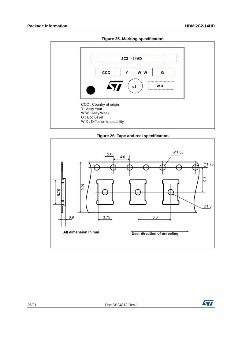
Figure 25. Marking specification
Figure 26. Tape and reel specification
2C2 -14HD
CCC Y W W G
e3 W X
CCC : Country of origin
Y : Assy YearW W : Assy WeekG : Eco Level
W X : Diffusion traceability
8.0
2.0
16
.06.7
5
7.5
3.75
4.0
Ø1.55
1.75
0.9
User direction of unreelingAll dimension in mm
Ø1.5
DocID024813 Rev1 27/31
HDMI2C2-14HD Recommendation on PCB assembly
31
5 Recommendation on PCB assembly
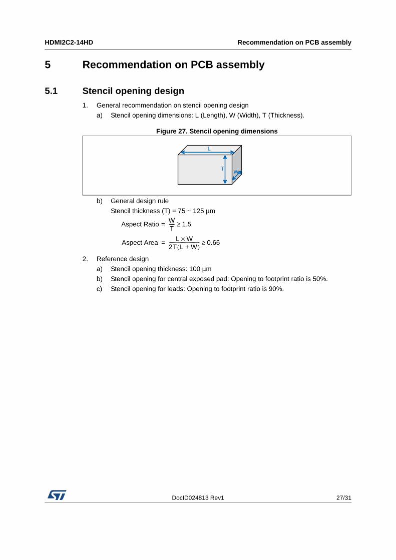
5.1 Stencil opening design1. General recommendation on stencil opening design
a) Stencil opening dimensions: L (Length), W (Width), T (Thickness).
Figure 27. Stencil opening dimensions
b) General design rule
Stencil thickness (T) = 75 ~ 125 µm
2. Reference design
a) Stencil opening thickness: 100 µm
b) Stencil opening for central exposed pad: Opening to footprint ratio is 50%.
c) Stencil opening for leads: Opening to footprint ratio is 90%.
L
TW
Aspect Ratio WT----- 1.5≥=
Aspect AreaL W×
2T L W+( )---------------------------- 0.66≥=
Recommendation on PCB assembly HDMI2C2-14HD
28/31 DocID024813 Rev1
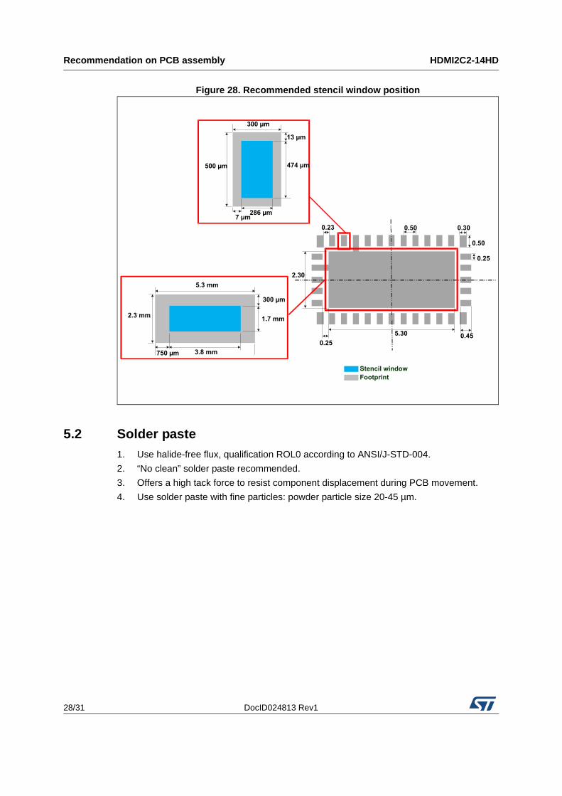
Figure 28. Recommended stencil window position
5.2 Solder paste1. Use halide-free flux, qualification ROL0 according to ANSI/J-STD-004.
2. “No clean” solder paste recommended.
3. Offers a high tack force to resist component displacement during PCB movement.
4. Use solder paste with fine particles: powder particle size 20-45 µm.
0.50 0.30
0.50
0.25
5.30
0.25
Stencil window
Footprint
0.45
0.23
286 µm
3.8 mm
300 µm
5.3 mm
7 µm
750 µm
2.30
474 µm
1.7 mm
13 µm
300 µm
500 µm
2.3 mm
DocID024813 Rev1 29/31
HDMI2C2-14HD Recommendation on PCB assembly
31
5.3 Placement1. Manual positioning is not recommended.
2. It is recommended to use the lead recognition capabilities of the placement system, not the outline centering.
3. Standard tolerance of ± 0.05 mm is recommended.
4. 3.5 N placement force is recommended. Too much placement force can lead to squeezed out solder paste and cause solder joints to short. Too low placement force can lead to insufficient contact between package and solder paste that could cause open solder joints or badly centered packages.
5. To improve the package placement accuracy, a bottom side optical control should be performed with a high resolution tool.
6. For assembly, a perfect supporting of the PCB is recommended during solder paste printing, pick and place and reflow soldering by using optimized tools.
5.4 PCB design preference1. To control the solder paste amount, closed vias are recommended instead of open
vias.
2. The position of tracks and open vias in the solder area should be well balanced. Symmetrical layout is recommended, in case any tilt phenomena caused by asymmetrical solder paste amount due to the solder flow away.
5.5 Reflow profile
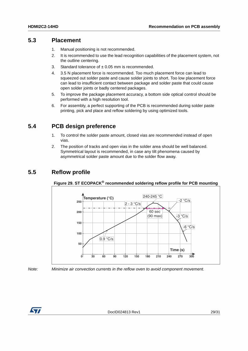
Figure 29. ST ECOPACK® recommended soldering reflow profile for PCB mounting
Note: Minimize air convection currents in the reflow oven to avoid component movement.
250
0
50
100
150
200
240210180150120906030 300270
-6 °C/s
240-245 °C
2 - 3 °C/s
Temperature (°C)-2 °C/s
-3 °C/s
Time (s)
0.9 °C/s
60 sec(90 max)
Ordering information HDMI2C2-14HD
30/31 DocID024813 Rev1
6 Ordering information
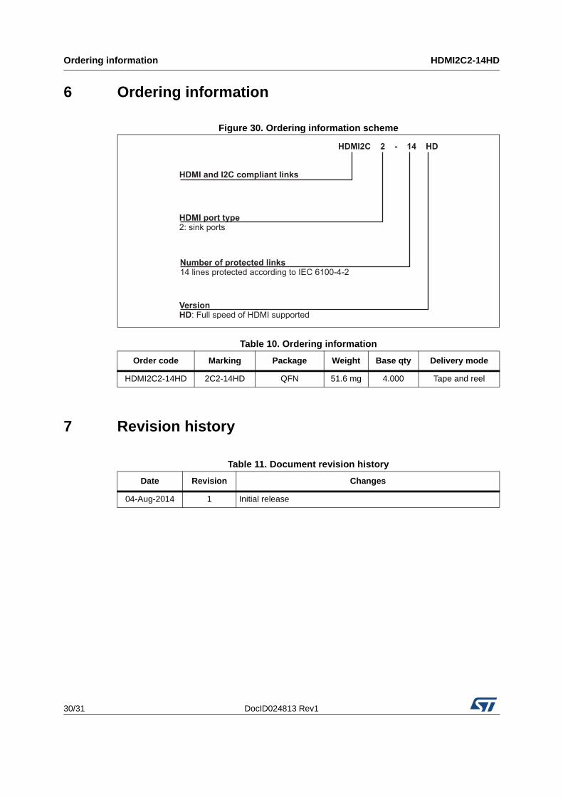
Figure 30. Ordering information scheme
7 Revision history
Table 10. Ordering information
Order code Marking Package Weight Base qty Delivery mode
HDMI2C2-14HD 2C2-14HD QFN 51.6 mg 4.000 Tape and reel
HDMI2C 2 - 14 HD
HDMI and I2C compliant links
Number of protected links14 lines protected according to IEC 6100-4-2
VersionHD: Full speed of HDMI supported
HDMI port type2: sink ports
Table 11. Document revision history
Date Revision Changes
04-Aug-2014 1 Initial release
DocID024813 Rev1 31/31
HDMI2C2-14HD
31
IMPORTANT NOTICE – PLEASE READ CAREFULLY
STMicroelectronics NV and its subsidiaries (“ST”) reserve the right to make changes, corrections, enhancements, modifications, and improvements to ST products and/or to this document at any time without notice. Purchasers should obtain the latest relevant information on ST products before placing orders. ST products are sold pursuant to ST’s terms and conditions of sale in place at the time of order acknowledgement.
Purchasers are solely responsible for the choice, selection, and use of ST products and ST assumes no liability for application assistance or the design of Purchasers’ products.
No license, express or implied, to any intellectual property right is granted by ST herein.
Resale of ST products with provisions different from the information set forth herein shall void any warranty granted by ST for such product.
ST and the ST logo are trademarks of ST. All other product or service names are the property of their respective owners.
Information in this document supersedes and replaces information previously supplied in any prior versions of this document.
© 2014 STMicroelectronics – All rights reserved