escholarship uc item 64v1x7jj
DESCRIPTION
gfdgdfTRANSCRIPT

eScholarship provides open access, scholarly publishingservices to the University of California and delivers a dynamicresearch platform to scholars worldwide.
Electronic Theses and DissertationsUC Riverside
Peer Reviewed
Title:2D Dirac Materials: From Graphene to Topological Insulators
Author:Teweldebrhan, Desalegne Bekuretsion
Acceptance Date:2011
Series:UC Riverside Electronic Theses and Dissertations
Degree:Ph.D., Electrical EngineeringUC Riverside
Advisor(s):Balandin, Alexander A
Committee:Khitun, Alexander, Lake, Roger
Permalink:http://escholarship.org/uc/item/64v1x7jj
Abstract:
Copyright Information:All rights reserved unless otherwise indicated. Contact the author or original publisher for anynecessary permissions. eScholarship is not the copyright owner for deposited works. Learn moreat http://www.escholarship.org/help_copyright.html#reuse

UNIVERSITY OF CALIFORNIA
RIVERSIDE
2D Dirac Materials: From Graphene to Topological Insulators
A Dissertation submitted in partial satisfaction
of the requirements for the degree of
Doctor of Philosophy
in
Electrical Engineering
by
Desalegne Bekuretsion Teweldebrhan
June 2011
Dissertation Committee:
Dr. Alexander A. Balandin, Chairperson
Dr. Roger Lake
Dr. Alexander Khitun

Copyright by
Desalegne Bekuretsion Teweldebrhan
2011

The Dissertation of Desalegne Bekuretsion Teweldebrhan is approved by:
_______________________________________________
_______________________________________________
_______________________________________________
Committee Chairperson
University of California, Riverside

iv
Acknowledgements
I would like to first acknowledge and express my sincere gratitude to my doctoral advisor
Prof. Alexander Balandin, for his guidance and expertise during my graduate experience.
I am appreciative for the support, kindness, patience, and professionalism he has always
presented me with throughout my study. Prof. Balandin is one of the most respected and
active researchers in our field. Throughout my studies I challenged myself to reach the
high-quality research standards and work ethics he expected from his research group and
staff. In the last few years, under his advisory, I was exposed to a world that very few
people with my background could imagine existed. There is no doubt in my mind that
the distinguished lessons and experiences he has equipped me with will always stay with
me throughout my future endeavors. Thank you Prof. Balandin.
I would like to thank Prof. Roger Lake and Prof. Alexander Khitun for serving on
my PhD dissertation committee. Their input and feedback of my research work lead to
several fruitful discussions that I found beneficial for my studies.

v
I am grateful to the great lab members of Prof. Balandin‟s Nano-Device
Laboratory (NDL). I would like to thank past students; Farough Parvizi, Dr. Suchismita
Ghosh, Dr. Qinghui Shao, Dr. Muhammad Rahman and Dr. Irene Calizo, as well as
current students Guanxiong Liu, Viveck Goyal, Craig Nolen, Md. Zahid Hossain, Farhan
Shahil, and Javed Khan for their help and contributions towards my research work. I
would also like to thank Dr. Dmitri Kotchetkov, Dr. Samia Sabrina, Dr. Denis Nika, Dr.
Igor Bejenari, Jie Yu, and Zhong Yan for useful research discussions.
I am thankful to Prof. Roland Kawakami and his group in the Physics Department
for their continuous support over the years. As an undergraduate, I worked with Prof.
Kawakami and his students Kyle Pi, Richard Chiang, Yan Li, Ramesh Thamankar, and
Wei-Hua Wang and was given the opportunity to take part in several fundamental science
and experimental design projects. These projects exposed me to the world of nanoscale
physics and materials growth methods, which became essential for my future graduate
studies. Thank you to Wei Han, Jairo Velasco Jr., Kathy McCreary and Jared Wong for
making my experiences there that much more fun and interesting.
Thank you to Maria Franco-Aguilar of UC Riverside's Graduate Division for
being very supportive and helpful throughout my studies. These included her help in
locating undergraduate research opportunities and my acquiring of a National Science
Foundation Graduate Fellowship.
vi
As always, I am thankful to my loving and supportive family. Thank you to my
parents, Bekuretsion and Ainealem, whose unconditional love, prayers, and leadership
have guided me and my siblings towards wanting to become productive members of
society. They have always made sure I knew to keep my feet grounded, by reminding me
of the all the responsibilities I have to carry on my shoulders. Thank you to my sister
Letekidan and younger brothers Tesfay, Yonas and Mehari for all our joyful moments
together. This dissertation is also dedicated to them.
Finally, all praises goes to God for blessing me with the ability to take on and
complete my studies. His graces have allowed me to meet many great people during this
journey of mine and I share this honor with them.

vii
To My Parents,
Bekuretsion and Ainealem
viii
ABSTRACT OF THE DISSERTATION
2D Dirac Materials: From Graphene to Topological Insulators
by
Desalegne Bekuretsion Teweldebrhan
Doctor of Philosophy, Graduate Program in Electrical Engineering
University of California, Riverside, June 2011
Professor Alexander A. Balandin, Chairperson
Silicon has been reaching physical limits as the semiconductor industry moves to smaller
device feature sizes, increased integration densities and faster operation speeds. There is a
strong need to engineer alternative materials, which can become foundation of new
computational paradigms or lead to other applications such as efficient solid-state energy
conversion. Recently discovered Dirac materials, which are characterized by the liner
electron dispersion, are examples of such alternative materials. In this dissertation, I
investigate two representatives of Dirac materials – graphene and topological insulators.
Specifically, I focus on the (i) effects of electron beam irradiation on graphene properties
and (ii) electronic and thermal characteristics of exfoliated films of Bi2Te3-family of

ix
topological insulators. I carried out Raman investigation of changes in graphene crystal
lattice induced by the low and medium energy electron-beam irradiation (5–20 keV). It
was found that radiation exposures result in appearance of the disorder D band around
1345 cm−1
. The dependence of the ratio of the intensities of D and G peaks, I(D)/I(G), on
the irradiation dose is non-monotonic suggesting graphene‟s transformation to
polycrystalline and then to disordered state. By controlling the irradiation dose one can
change the carrier mobility and increase the resistance at the minimum conduction point.
The obtained results may lead to new methods of defect engineering of graphene
properties. They also have important implications for fabrication of graphene nano-
devices, which involve electron beams. Bismuth telluride and related compounds are the
best thermoelectric materials known today. Recently, it was determined that they reveal
the topological insulator properties. We succeeded in the first “graphene-like” exfoliation
of large-area crystalline films and ribbons of Bi2Te3 with the thickness going down to a
single quintuple. The presence of van der Waals gaps allowed us to disassemble Bi2Te3
crystal into the five mono-atomic sheets consisting of Te(1)
-Bi-Te(2)
-Bi-Te(1)
. The
exfoliated films had extremely low thermal conductivity and electrical resistance in the
range required for thermoelectric applications. The obtained results may pave the way for
producing Bi2Te3 films and stacked superlattices with strong quantum confinement of
charge carriers and predominantly surface transport, and allow one to obtain theoretically
predicted order-of-magnitude higher thermoelectric figure-of-merit.

x
Contents
List of Figures xiii
List of Tables xviii
1 Introduction 1
1.1 Motivations . . . . . . . . . . . . . . . . . . . . . . . . . . . . . . . . . . . . . . . . . . . . . . . . . . 1
1.2 Dirac Materials . . . . . . . . . . . . . . . . . . . . . . . . . . . . . . . . . . . . . . . . . . . . . . . . 5
1.2.1 Graphene . . . . . . . . . . . . . . . . . . . . . . . . . . . . . . . . . . . . . . . . . . . . . 7
1.2.2 Bi2Te3 Based Materials . . . . . . . . . . . . . . . . . . . . . . . . . . . . . . . . . . 10
1.3 Confined Nanostructures . . . . . . . . . . . . . . . . . . . . . . . . . . . . . . . . . . . . . . . . 15
1.3.1 Quantum Wells . . . . . . . . . . . . . . . . . . . . . . . . . . . . . . . . . . . . . . . . 15
References . . . . . . . . . . . . . . . . . . . . . . . . . . . . . . . . . . . . . . . . . . . . . . . . . . 17
2 Experimental Setup 19
2.1 Thin Film Synthesis and Fabrication Methods . . . . . . . . . . . . . . . . . . . . . . . 19
2.2 Raman Spectroscopy . . . . . . . . . . . . . . . . . . . . . . . . . . . . . . . . . . . . . . . . . . . 24
2.1.1 Raman Spectrum of Carbon Materials. . . . . . . . . . . . . . . . . . . . . . . 27
2.3 Electrical Transport . . . . . . . . . . . . . . . . . . . . . . . . . . . . . . . . . . . . . . . . . . . 29
References . . . . . . . . . . . . . . . . . . . . . . . . . . . . . . . . . . . . . . . . . . . . . . . . . . . 31

xi
3 Graphene Preparation and Characterization 33
3.1 Preparation Methods of Atomically-Thin 2D Graphene . . . . . . . . . . . . . . . 33
3.2 Raman Spectroscopy of Graphene . . . . . . . . . . . . . . . . . . . . . . . . . . . . . . . . 34
3.2.1 Raman as Nanometrology Tool for Graphene . . . . . . . . . . . . . . . . . 36
3.3 Experimental Results . . . . . . . . . . . . . . . . . . . . . . . . . . . . . . . . . . . . . . . . . . 38
3.3.1 Synthesis using HPHT Method . . . . . . . . . . . . . . . . . . . . . . . . . . . 39
3.3.2 Raman Detection of DNA Polymers . . . . . . . . . . . . . . . . . . . . . . . . 46
3.3.3 Thermal Characterization in Suspended Graphene . . . . . . . . . . . . . 47
3.4 Discussion . . . . . . . . . . . . . . . . . . . . . . . . . . . . . . . . . . . . . . . . . . . . . . . . . . . 51
3.5 Summary . . . . . . . . . . . . . . . . . . . . . . . . . . . . . . . . . . . . . . . . . . . . . . . . . . . . 52
References . . . . . . . . . . . . . . . . . . . . . . . . . . . . . . . . . . . . . . . . . . . . . . . . . . . 54
4 Low-Energy Electron-Beam Irradiation Effects on
Graphene and Graphene Devices 56
4.1 Motivations . . . . . . . . . . . . . . . . . . . . . . . . . . . . . . . . . . . . . . . . . . . . . . . . . . 56
4.2 Defects and Disorder in Carbon Materials . . . . . . . . . . . . . . . . . . . . . . . . . . 57
4.2.1 Raman Spectrum of Irradiated Graphene . . . . . . . . . . . . . . . . . . . . 58
4.3 Experimental Results . . . . . . . . . . . . . . . . . . . . . . . . . . . . . . . . . . . . . . . . . . 58
4.3.1 Graphene Susceptibility to Electron-Beam Irradiation . . . . . . . . . . 59
4.3.2 Raman Spectrum of Irradiated Graphene . . . . . . . . . . . . . . . . . . . . 61
4.3.2.1 Non-monotonic ID/IG Defect Concentration . . . . . . . . . . 63
4.3.3 Selective Irradiation and Nano-Patterning of Graphene . . . . . . . . . 69
4.3.4 Tuning of Graphene Devices via Electron Irradiation. . . . . . . . . . . 72
4.3.5 Thermal Reversibility in Irradiated Graphene . . . . . . . . . . . . . . . . 77
4.4 Summary . . . . . . . . . . . . . . . . . . . . . . . . . . . . . . . . . . . . . . . . . . . . . . . . . . . 82
References . . . . . . . . . . . . . . . . . . . . . . . . . . . . . . . . . . . . . . . . . . . . . . . . . . 84

xii
5 Mechanical Exfoliation of Atomically-Thin Bi2Te3 Films 87
5.1 Motivations . . . . . . . . . . . . . . . . . . . . . . . . . . . . . . . . . . . . . . . . . . . . . . 87
5.2 Bi2Te3 Crystal Structure and Van der Waal Gaps . . . . . . . . . . . . . . . . . 90
5.3 Experimental Results. . . . . . . . . . . . . . . . . . . . . . . . . . . . . . . . . . . . . . . 91
5.3.1 Exfoliation and Characterization . . . . . . . . . . . . . . . . . . . . . . . 91
5.3.2 Atomically-Thin Crystal Characterization . . . . . . . . . . . . . . . . 93
5.3.3 Raman Spectroscopy Characterization of Bi2Te3 and Bi2Se3. . . 98
5.3.4 Electrical Properties of Exfoliated 2D Films . . . . . . . . . . . . . . 105
5.3.5 2D Topological Insulators. . . . . . . . . . . . . . . . . . . . . . . . . . . . . 109
5.3.6 Thermal Conductivity of Stacked Bi2Te3 Films. . . . . . . . . . . . . 109
5.4 Summary . . . . . . . . . . . . . . . . . . . . . . . . . . . . . . . . . . . . . . . . . . . . . . . 112
References . . . . . . . . . . . . . . . . . . . . . . . . . . . . . . . . . . . . . . . . . . . . . . 115
6 Concluding Remarks 119

xiii
List of Figures
1.1 Plot of number of transistors and power density on a chip between the
years1970 and 2010. Plot from data provided by Intel Corporation. . . . . . . . .
1.2 Plot indicates the increasing trends of heat flux produced from bipolar and
CMOS transistor architecture generations. . . . . . . . . . . . . . . . . . . . . . . . . . . . .
1.3 On the left is an illustration of the energy dispersion dependence for charges
in a typical metal that tends to follow Schrödinger Equation and have a
quadratic dependence to momentum. On the right is the dispersion relation
for Dirac electrons which posses a linear Dirac-like dependence. . . . . . . . . . .
1.4 Crystal structures of Graphene which has two atoms per unit cell, which
account for two Dirac points per Brillouin zone. Both are located at the two
inequivalent Brillion zone corners (k and k‟) of its reciprocal lattice structure
as shown on the right . . . . . . . . . . . . . . . . . . . . . . . . . . . . . . . . . . . . . . . . . . . . .
1.5 Energy band structure of graphene. The energy bands become cone shaped
at the corner Dirac points at K and K‟. Here the conductance band touches
valence band . . . . . . . . . . . . . . . . . . . . . . . . . . . . . . . . . . . . . . . . . . . . . . . . . . .
1.6 Graphene‟s ambipolar behavior change carriers with voltage bias. . . . . . . . . .
1.7 Schematic of Bi2Te3 crystal structure of D3d5
– R(-3)m space group showing
positions of Bi and Te atoms in a single five-fold quintuple layer. . . . . . . . . .
1.8 An idealized band structure for a topological insulator. The Dirac cone falls
within the gamma point of the first Brillioun zone for the topologically
protected surface states. . . . . . . . . . . . . . . . . . . . . . . . . . . . . . . . . . . . . . . . . . . x
2
d
4
1.3
1.3
6
1.3
1.3
1.3
8
1.3
1.3
9
10
1.3
12
1.3
1.3
13

xiv
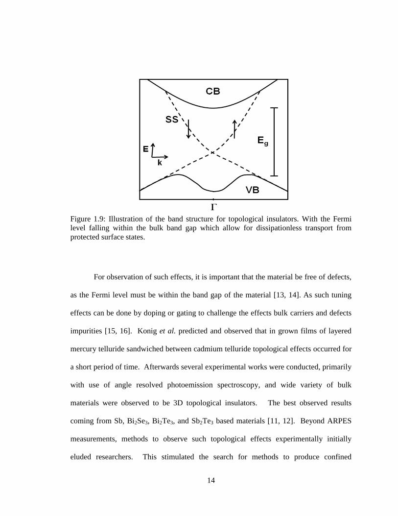
1.9 Illustration of the band structure for topological insulators. With the Fermi
level falling within the bulk band gap which allow for dissipationless
transport from protected surface states. . . . . . . . . . . . . . . . . . . . . . . . . . . . . . . x
1.10 Electronic density of states modifications for a) bulk 3D crystalline
semiconductors, b) 2D quantum wells, c) 1D nanowires or nanotubes, and
d) 0D quantum dots. Low dimensionality of materials also exhibits other
physical phenomena, other than a density of electronic states (DOS) there
may be useful for enhancing thermoelectric performance . . . . . . . . . . . . . . . . x
2.1 Images of a mechanically exfoliated thin graphitic flake in optical (left) and
scanning electron (right) microscopes. Few-layer graphene is clearly visible
in SEM but not easily in optically . . . . . . . . . . . . . . . . . . . . . . . . . . . . . . . . . . .
2.2 Rayleigh, Stokes, and Anti-Stokes scattering processes at the same laser
frequency (below). Here the energy relationship of the photon during
Rayleigh, Stokes, and anti-Stokes scattering is illustrated (top) . . . . . . . . . . . .
3.1 Raman spectrum of a nanographite sample. The G peak and 2D (G‟) bands
that were taken with laser excitation energy of 2.41 eV (= 488nm). . . . . . . . x
3.2 Raman spectrum of single, bilayer, 3-layer, 4-layer, and 5-layer graphene.
Intensity ratio of 2D band to G peak for few-layer graphene is suppressed
compared to single layer graphene. . . . . . . . . . . . . . . . . . . . . . . . . . . . . . . . .. . x
3.3 2D band for SLG and BLG on a Si/SiO2 substrate. Based on the number of
Lorentzian elemental peaks in the deconvolution of SLG and BLG spectrums
are explained by the double-resonance model. . . . . . . . . . . . . . . . . . . . . . . . . . x
3.4 (a) Schematic of the graphene growth “cylinder”; (b) illustration of the high
pressure – high temperature growth in the “split sphere” apparatus; (c) image
of the cylinder with the material after it was removed from the growth
chamber. Note that the region in the center, near the seed, is uniform
indicating crystalline layers while the material at the edges is rough
amorphous carbon. . . . . . . . . . . . . . . . . . . . . . . . . . . . . . . . . . . . . . . . . . . . . . . x
3.5 (a) Optical image of the HPHT grown graphene flakes. The gray – green
color regions correspond to single layer graphene while yellowish regions are
bulk graphitic pieces. (b) Scanning electron microscopy image of the edges
of a large graphene flake with the dimensions of ~ 10 m x 3 m produced
via the HPHT growth. The SEM inspection confirmed the uniformity of
graphene layers. . . . . . . . . . . . . . . . . . . . . . . . . . . . . . . . . . . . . . . . . . . . . . . . . x
3.6 Raman spectrum of the single layer graphene (a) and few-layer graphene (b)
produced via the HPHT melting growth process with Fe-Ni catalysts. The
shape and location of the G peak and 2D band were used to count the layers.
1.3
1.3
14
1.3
1.3
1.3
1.3
16
1.3
1.3
22
1.3
26
1.3
35
1.3
1.3
36
1.3
1.3
37
1.3
1.3
1.3
1.3
1.3
42
1.3
1.3
1.3
1.3
1.3
43
1.3
1.33
1.33

xv
The absence of the disorder D band near 1350 cm-1
attests to the high quality
of the grown graphene . . . . . . . . . . . . . . . . . . . . . . . . . . . . . . . . . . . . . . . . . . .
3.7 Raman spectrum of the initial natural bulk graphite source, as-produced
HPHT graphitic layers and single-layer graphene in the G-peak region. Note
that the disorder-induced D band is very strong in the spectra of the initial
bulk graphite and it is completely absent in the spectra of graphene. This
suggests the material quality improves during the growth process via melting
and re-crystallization. . . . . . . . . . . . . . . . . . . . . . . . . . . . . . . . . . . . . . . . . . . . .
3.8 Micro-Raman spectroscopy of the signature G-peak and 2D band for pristine
graphene and DNA/graphene based system. In (a) the G-peak centered at
1580 cm-1
, seen at 488nm excitation wavelength, shifts and average 2cm-1
after DNA coating. (b) Second order 2D band shifts by a value of ~4 cm-1
as
a result of DNA coating. Both signature peaks also show relative shortening
of their respective full width half max values (FWHM) as a result of coating
as well. . . . . . . . . . . . . . . . . . . . . . . . . . . . . . . . . . . . . . . . . . . . . . . . . . . . . . . .
3.9 The shift in G-peak spectral position vs. change in total dissipated power.
The slope of the dependence is used for the extraction of the thermal
conductivity of graphene . . . . . . . . . . . . . . . . . . . . . . . . . . . . . . . . . . . . . . . . .
4.1 AFM topography indicates differences between irradiated and non-irradiated
graphene . . . . . . . . . . . . . . . . . . . . . . . . . . . . . . . . . . . . . . . . . . . . . . . . . . . . . .
4.2 SEM of selected single layer and bilayer regions within fixed exposure area. X
4.3 Raman spectra of graphene before and after e-beam irradiation under 488 nm
and 633 nm laser excitation. . . . . . . . . . . . . . . . . . . . . . . . . . . . . . . . . . . . . . . . x
4.4 First order and second order Raman spectrums for Irradiated graphene . . . . .
4.5 Evolution of the ratio of the intensities of the D andG peaks as a function of
the irradiation exposure for single layer (SLG) in red and bilayer graphene
(BLG) in black. Using Tuintra-Koening relation of grain size to Irradiation
fluence was determined. . . . . . . . . . . . . . . . . . . . . . . . . . . . . . . . . . . . . . . . . . . x
4.6 Evolution of the ratio of the intensities of the D andG peaks as a function of
the irradiation for single layer (SLG) giving a 1/T like dependence for up to
2hrs of irradiation.. . . . . . . . . . . . . . . . . . . . . . . . . . . . . . . . . . . . . . . . . . . . . . . x
4.7 I(D)/I(G) ratio for irradiation under 30 pA is shown. These trends suggest
the graphene experience a structure change from graphene to nano-
crystalline graphene. . . . . . . . . . . . . . . . . . . . . . . . . . . . . . . . . . . . . . . . . . . . . .
4.8 Selective area irradiation using e-beam to pattern regions of single layer
graphene. (a) Optical image of single layer graphene region and schematics
ddd
43
1.3
1.3
1.3
1.3
1.3
45
1.3
1.3
1.3
1.3
1.3
1.3
47
1.3
1.3
50
1.3
57
X59
1.3
62
63
1.3
1.3
1.3
65
1.3
1.3
65
1.3
1.3
67
1.3
1.3

xvi
illustrating controlled irradiational sectioning of regions. Raman spectra
mappings of respective G-Peak, 2D-band, D-peak, and ID/IG ratio both prior
(b) and post (c) electron beam irradiation. It can be seen that the single layer
regions are more susceptible to irradiation than the single layer regions . . . . .
4.9 Three possible mechanisms for E-beam patterning methods of single layer
graphene. (i) Direct contact metal on graphene, (ii) Masking shadowing, or
even as we have demonstrated (iii) direct writing . . . . . . . . . . . . . . . . . . . . . .
4.10 Transfer characteristics of SLG evolution with increasing dosage of
irradiation. The irradiation dosage for each step is noted. The inset is the
optical image of a typical graphene device. The metal electrodes are used as
source and drain, and heavily doped silicon is used as back gate electrode.
The light blue strip is graphene flake. The purple rectangular region is the
irradiation area which covers all the graphene part between source and drain
while excludes two electrodes in case of any possible changes of contact
brought by the irradiation in the experiment. . . . . . . . . . . . . . . . . . . . . . . . . . . x
4.11 Mobility of three SLG devices decreases almost linearly with irradiation
dosage. After the 4th
The inset shows fitting result of one device. . . . . . . . . . x
4.12 Evolution of SLG resistivity with irradiation dosage. Inset shows the effect
of e-beam irradiation on charge impurity density for SLG . . . . . . . . . . . . . . . x
4.13 a) SLG devices is altered as the annealing is incorporated during the process
at ~500K. b) The diminishing effect due to annealing of the I(D)/I(G) ratio,
can be seen indicated in red between irradiation trials 1-2, 4-5, and 7-8. . . . .
5.1 Schematic of Bi2Te3 crystal structure of D3d5
– R(-3)m space group showing
quintuple layers and location of the van der Waals gaps. The Te(1)
-Te(1)
bond
is the weakest while Bi-Te(1)
bond is the strongest. The mechanical
exfoliation mostly results in breaking the Te(1)
-Te(1)
van der Waals bond and
formation of quintuples although in some cases intra-quintuples bonds also
break leading to bi-atomic and tri-atomic layers. . . . . . . . . . . . . . . . . . . . . . .
5.2 Images of quasi-2D bismuth telluride crystals showing (a) SEM micrograph
of the overlapping few-layer Bi-Te atomic crystals; (b) large-area atomically-
thin crystal attached to thick Bi2Te3 film; (c) suspended films with visible
quasi-2D layers; (d) suspended few-atom-plane film; (e) AFM micrograph of
few-atomic-layer steps in the cleaved films; and (f) TEM micrograph of the
quasi-2D bismuth telluride film . . . . . . . . . . . . . . . . . . . . . . . . . . . . . . . . . . . .
5.3 Structural and compositional characterization data showing (a) electron
diffraction pattern indicating that quasi-2D Bi-Te films are crystalline;
(b) EDS spectrum of the suspended atomic film of bismuth telluride; and
(c) EDS spectrum of the reference thick film. Note that the dominant peaks
1.3
1.3
1.3
69
1.3
1.3
71
1.3
1.3
1.3
1.3
1.3
1.3
1.3
74
1.3
75
1.3
76
1.3
1.3
78
1.3
1.3
1.3
1.3
1.3
91
1.3
1.3
1.3
1.3
1.3
96
1.3
1.3
1.3
1.3

xvii
in the EDS spectrum of the quasi-2D Bi-Te film shown in (b) are those of Si
and O proving transparency of the atomic film for the electron beam. These
peaks are absent in the spectrum of the reference bulk Bi2Te3 . . . . . . . . . . . . .
5.4 Raman spectra of quasi-2D bismuth telluride crystals. (a) SEM image
showing suspended Bi-Te atomic film, which rests partially on SiO2 and Si
regions of the substrate. The spectra from the suspended and supported
regions were recorded in the locations marked as 1, 2, and 3. (b) Informative
Raman bands in the spectra of Bi-Te atomic films recorded at very low
excitation power level. Note that the out-of-plane phonon modes in the
suspended atomic crystals have higher intensity. . . . . . . . . . . . . . . . . . . . . . . x
5.5 Evolution of Raman spectra from the Bi-Te atomic film with changing
intensity of the atomic Bi-Te crystals in sharp contrast to graphene. The inset
shows the spots from which the Raman spectra were recorded. . . . . . . . . . . . . x
5.6 Raman analysis of Bi2Se3 Surface Topography. . . . . . . . . . . . . . . . . . . . . . . . x
5.7 (a) Electrical current and resistivity of the quasi-2D bismuth telluride crystal
as functions of the applied source – drain bias. The inset shows an optical
microscopy image of the test structure. (b) Current as a function of
temperature in Bi-Te atomic crystals shown for different source – drain
voltages. Inset shows current – voltage characteristics in the low-bias region
for different temperature. . . . . . . . . . . . . . . . . . . . . . . . . . . . . . . . . . . . . . . . . .
5.8 Optical Image if few-layer bismuth telluride hall bar structure device. . . . . . .
1.3
1.3
97
1.3
1.3
1.3
1.3
1.3
1.3
99
1.3
1.3
101
104
1.3
1.3
1.3
1.3
1.3
106
106

xviii
List of Tables
1.1 The bond lengths between the atomic layers in Bi2Te3 quintuple layers.
There is a correlation between the bond lengths and bond strength . . . . . . . . .
2.1 From the deconvolution of the 2D band of few-layer graphene, layers can
be distinguished easily on standard SiO2/Si substrate . . . . . . . . . . . . . . . . . . .
4.1 The irradiation dosage (fluence) of electron beams on graphene at ~0.15nA
beam current. With all variables fixed the dosage is depended on exposure
time . . . . . . . . . . . . . . . . . . . . . . . . . . . . . . . . . . . . . . . . . . . . . . . . . . . . . . . . .
5.1: The Raman frequencies are provided for the main peaks for Bi2Te3 exfoliated
atomic crystalline films on Silicon, on Oxide (SiO2), and that are suspended.
Out of plane mode AII
1g is shown to enhance in suspended films. Surface
charges may be forming stronger effects in suspended films. . . . . . . . . . . . . .
1.3
24
1.3
1.3
38
1.3
1.3
1.3
61
Cxc
cxc
xcx
100
1
Chapter 1
Introduction
1.1 Motivations
Considered to be one of the greatest invention of the 20th
century, the transistor is the
most active component of all of modern technology. Experimentally first observed and
demonstrated by John Barseen, Walter Bratain, and William Shockley in 1947 at Bell
Labs, the transistor is a solid piece of semiconductor material with several contact
terminals that connect it to an external circuit. Although transistors can be packaged
individually, it wasn‟t till they were embedded into integrated circuits, vastly increasing
their functionality, that they helped revolutionize the electronics field to unprecedented
levels both technically and economically. In initial setups, several semiconductor
materials were used to produce transistors which included germanium, gallium arsenide,
silicon and even silicon carbide. Although it required higher melting temperatures and
was naturally reactive, silicon offered the best prospects for better performance,

2
especially in logic based applications. Silicon transistors had shown to have far less
leakage issues as compared to germanium, and in 1954 were the first commercially
available transistors developed by Texas Instruments. Today, our technology is
dependent on highly automated semiconductor processing methods based around silicon
to mass produce low cost per-volume transistors.
Figure 1.1: Plot of number of transistors and power density on a chip between the years
1970 and 2010. Plot from data provided by Intel Corporation.
As the basis roadmap of the semiconductor industry, Moore‟s Law has
continuously projected performance gain that have resulted in shrinking transistor gate
length, increase in number of transistors per wafer, wafer size growth, and reduction in
defect density reduction. Along with the ability to help predict technological

3
expectations, Moore‟s Law has also been associated with the growing number of
challenges from each new generation that the industry will continually need to address.
With high performance capacity, silicon-based contemporary metal oxide
semiconductor (Si-CMOS) based transistor architectures are the most common used in
today‟s electronics industry. Every two years, the industry makes changes to these
fundamental structures of the transistor on the basis of using a miniaturization process.
Also plotted, alongside the Moore‟s Law trend, in Figure 1.1 is the average power
densities of processors with advancements which have shown to increase within the chips
over the past 30 years. With miniaturization comes increased heat generation per unit
area and increase thermal resistance so better cooling systems are necessary for further
advancements in many technological application. Currently levels of heat generated in
processors exceed 100 watts/cm2, which can be categorized to be on the order, if not
greater, than the heat produced from a nuclear reactor. As shown in Figure 1.2, the past
shows that similar thermal issues were observed, prior to switching to CMOS
architecture, in bipolar type transistors.

4
Figure 1.2: Plot indicates the increasing trends of heat produced from different generation
of bipolar and CMOS architecture generations.
Currently, commercial products are available in the 45 nm and 32 nm technology
node regimes, while advancements towards 22 nm and lower features sizes have already
began production. As silicon based transistors reach physical and technological
limitations, continuous research towards novel material with extraordinary properties
have growingly been important to help meet the demands of the next generation of
devices [1]. In the field of material science and disciplines alike, extensive research
studies has been devoted into looking at alternative materials for devices integration with
current technology.
The transistor is made up of several materials with a variety of physical properties
that together allow for fast switching capabilities in the presence of an external field.
Traditionally, thin layers of several semiconducting material and high thermal
conductivity metal such copper have been used to construct such devices. The aggressive
downscaling of the feature sizes and compact integration for new and complex structures

5
continuously requires expensive replacement of tools and instrumentations. With that the
technology is being pushed to its limits, standard materials and new materials must both
be capable of being processed using state of the art lithography methods for device
fabrication. New and innovative ideas are also critical to meet the demands of device
miniaturization and patterning techniques. A promising approach has recently been to
look at incorporating materials with low dimensionalities that exhibit extraordinary
properties into the chip design to help improve the device ability to perform effectively.
1.2 Dirac Materials
Dirac materials are defined as a class of material who possess a unique Dirac-like cone
type of low-energy band structure within the first Brillioun zone. This allows for the
production of extraordinary electrons that are distinctive from standard electron produced
in metals. Typical electrons, like those found in standard metals, tend to behave like
massive particles and have a quadratic energy dependence on momentum. Such massive
electrons are said to obey Schrodinger‟s equation. Dirac electrons, on the other hand,
have energies that contain a linear dependence on momentum and follow Dirac
equations, see Figure 1.3. The linear dispersion will result in a d2/dk
2 = 0 according to
Eq. [1.1], which is used to determine the effective masse of electron in a material.
2
2
2*
11
dk
d
m
[1.1]

6
As a result, Dirac electrons behave like massless fermions which allow for ballistic
transport along the surface of the Dirac material. Unlike other massless particles though,
such as neutrinos, Dirac electrons have a charge. As a result, electrons in Dirac materials
are charged massless particles that can easily be influenced by an external magnetic field.
Figure 1.3: On the left is an illustration of the energy dispersion dependence for electrons
in a typical metal that tends to follow Schrödinger‟s Equation and have a quadratic
dependence to momentum. On the right is the dispersion relation for Dirac electrons
which posses a linear Dirac-like dependence.
This opens the door to some exotic physics and physical properties in Dirac
materials that are not found in typical materials, which may be utilized for a plethora of
future applications. The pseudospins in the momentum direction are called chirality,
which is used to refer to the additional built-in symmetry between electron and hole parts
in the spectrum. We will discuss two types of Dirac materials here as possible candidates
for future electronic application. These are single layer graphene and newly found Dirac

7
materials of bismuth telluride based topological insulator materials (i.e. Bi2Te3, Bi2Se3,
etc).
1.2.1 Graphene
Graphene, a single atomic layer of graphite, is a flat sheet of carbon atoms tightly
packed into a two-dimensional honeycomb lattice, and is a basic building block for
graphitic materials of all other dimensionalities i.e. 0D buckyballs, 1D nanotubes, or 3D
graphite. Theoretically, graphene has been studied for over sixty years, and is widely
used for describing properties of various carbon-based materials. The material had not
been considered to exist in the free standing state until it was reported by Andre Geim
and K.S. Novoselov from University of Manchester, UK in 2004 [2]. Both Geim and
Novoselov, would become recipients of the 2010 Noble Prize in Physics for their work
with the new material. Graphene is a source of remarkable electronic properties, one of
the reasons being its unique energy band structure. The electronic structure results from a
simple nearest neighbor, tight-binding approximation. As seen in Figure 1.4, Graphene
posses a two atoms per unit cell in its lattice structure which accounts for two conical
points per Brillouin zone, called the Dirac points located at the two inequivalent Brillion
zone corners (k and k‟). At these corners of the Brillouin zone, the valence and the
conduction band meet, with the Fermi energy level passing through these points. Energy
dispersion curve in the vicinity of these points can be approximated to introduce a linear

8
Figure 1.4: Crystal structures of Graphene which has two atoms per unit cell, which
accounts for two Dirac points per Brillouin zone. Both are located at the two inequivalent
Brillion zone corners (k and k‟) of its reciprocal lattice structure shown on the right.
relationship with momentum and is given by the Eq. [1.2],
kvikk
ikkvH f
yx
yxf
0
0 [1.2]
where vf is the Fermi velocity. Now, only graphene and its bilayer have such simple
electronic spectra, they are both zero-gap semiconductors. For three and more layers, the
spectra become increasingly complicated, where several charge carriers appear and the
conduction and valence bands start notably overlapping.
)0,3
1,1(
3
2'
)0,3
1,1(
3
2
o
o
aK
aK
)0,3,1(3
2
)0,3,1(3
2
2
1
o
o
ab
ab
)0,3,3(2
)0,3,3(2
2
1
o
o
aa
aa

9
Figure 1.5: Energy band structure of graphene. The energy bands become cone shaped at
the corner Dirac points at K and K‟. Here the conductance band touches valence band.
The interaction between electrons and the honeycomb lattice causes the electrons
to behave as if they have absolutely no mass. As a result, they are referred to as massless
relativistic Dirac fermions. The electron dynamics in graphene obey the 2D Dirac
equation, where the quantum mechanical description of electrons moving relativistically.
The speed of light is associated with the material by its Fermi velocity of vf = c/300. Thus
graphene could even be utilized effectively to study quantum field theory without the use
of a huge charge accelerator.
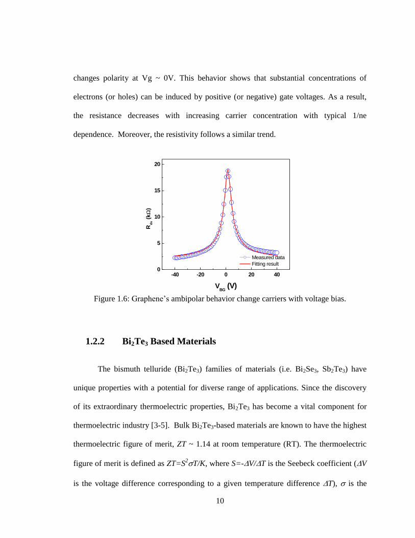
One of the most important merits of graphene is an ambipolar electric field effect.
Here, charge carriers can continuously be tuned between the electrons and holes which
may have mobilities that exceed 15000 cm2V
-1s
-1 at room temperature. This feature
makes graphene based devices achievable on silicon integrated circuits. In Figure 1.6,
it‟s shown the effect an electric field has on a graphene device. The hall resistivity
10
-40 -20 0 20 400
5
10
15
20
Rd
s (
k
)
VBG
(V)
Measured data
Fitting result
changes polarity at Vg ~ 0V. This behavior shows that substantial concentrations of
electrons (or holes) can be induced by positive (or negative) gate voltages. As a result,
the resistance decreases with increasing carrier concentration with typical 1/ne
dependence. Moreover, the resistivity follows a similar trend.
Figure 1.6: Graphene‟s ambipolar behavior change carriers with voltage bias.
1.2.2 Bi2Te3 Based Materials
The bismuth telluride (Bi2Te3) families of materials (i.e. Bi2Se3, Sb2Te3) have
unique properties with a potential for diverse range of applications. Since the discovery
of its extraordinary thermoelectric properties, Bi2Te3 has become a vital component for
thermoelectric industry [3-5]. Bulk Bi2Te3-based materials are known to have the highest
thermoelectric figure of merit, ZT ~ 1.14 at room temperature (RT). The thermoelectric
figure of merit is defined as ZT=S2T/K, where S=-V/T is the Seebeck coefficient (V
is the voltage difference corresponding to a given temperature difference T), is the

11
electrical conductivity and K is the thermal conductivity, which has contributions from
electrons and phonons. It is clear from ZT definition that in order to improve
thermoelectric figure of merit one should increase the thermopower S2 and decrease the
thermal conductivity. Different approaches have been attempted in order to enhance the
thermoelectric properties of Bi2Te3 or its alloys. These approaches included change in
stoichiometry, the use of polycrystalline materials with different grain sizes, intentional
introduction of structural defects and incorporation of different dopants, e.g. Sb or Se,
into Bi2Te3 lattice. The optimization of bulk Bi2Te3 led to incremental improvements but
no breakthrough enhancement in ZT was achieved.
Bi2Te3 has the rhombohedral crystal structure of the space group D3d5
– R(-3)m
with five atoms in one unit cell. The lattice parameters of the hexagonal cells of Bi2Te3
are aH= 0.4384 nm and cH = 3.045 nm [6]. Its atomic arrangement can be visualized in
terms of the layered sandwich structure (see Figure 1.7 below). Each sandwich is built up
by five mono-atomic sheets, referred to as quintuple layers, along the cH axis with the
sequence – [Te(1)
-Bi-Te(2)
-Bi-Te(1)
] – [Te(1)
-Bi-Te(2)
-Bi-Te(1)
] –. Here superscripts (1)
and (2) denote two different chemical states for the anions.

12
Figure 1.7: Schematic of Bi2Te3 crystal structure of D3d5
– R(-3)m space group showing a
positions of Bi and Te atoms in a single five-fold quintuple layer.
Topological insulators is a relatively new and exciting area that looks at materials
which have a bulk insulating gap and conducting surface states that are topologically
protected against scattering by the time-reversal symmetry. This newly discovered class
of materials was predicted to reveal many unique properties, e.g. quantum-Hall-like
behavior in the absence of magnetic field. Some of these properties have already been
demonstrated, stimulating interest into topological insulators as possible materials for
quantum computing and magnetic memory with pure electrical read-write operations. As
topological insulators, surface states of certain crystals are predicted to consist of a single
Dirac cone. Moreover, it has been shown that the layered structures of Bi2Te3 and related
materials such as Bi2Se3 and Sb2Te3 are also topological insulators [7-9].

13
The particles in topological insulators coated with thin ferromagnetic layers have
manifested exotic physics and were proposed for possible applications in the magnetic
memory where write and read operations are achieved by purely electric means.
Figure 1.8: An idealized band structure for a topological insulator. The Dirac cone falls
within the gamma point of the first Brillioun zone for the topologically-protected surface
states.
Behind its theoretical physics, topological insulators are fundamentally described
as material that behave as complete insulator within its interior while allowing ballistic
transport of charges on its boundary. In the interior of a bulk three dimensional
topological materials the electric band structure would be like that of any other insulator
with the Fermi level being within its band gap. Now theoretically it has been determined
that at the surface and edges, special states lie with the bulk band gap which allow for
conduction of carriers. These carriers are allowed protected ballistic transport when their
spin states are aligned and opposite with their momentums, which restricts scattering
from occurring at particular energies as shown in Figure 1.9 [8, 10].
14
Figure 1.9: Illustration of the band structure for topological insulators. With the Fermi
level falling within the bulk band gap which allow for dissipationless transport from
protected surface states.
For observation of such effects, it is important that the material be free of defects,
as the Fermi level must be within the band gap of the material [13, 14]. As such tuning
effects can be done by doping or gating to challenge the effects bulk carriers and defects
impurities [15, 16]. Konig et al. predicted and observed that in grown films of layered
mercury telluride sandwiched between cadmium telluride topological effects occurred for
a short period of time. Afterwards several experimental works were conducted, primarily
with use of angle resolved photoemission spectroscopy, and wide variety of bulk
materials were observed to be 3D topological insulators. The best observed results
coming from Sb, Bi2Se3, Bi2Te3, and Sb2Te3 based materials [11, 12]. Beyond ARPES
measurements, methods to observe such topological effects experimentally initially
eluded researchers. This stimulated the search for methods to produce confined

15
nanostructure forms of quasi-2D crystalline forms of topological insulator based
materials for even further enhance methods of characterizing such effects.
1.3 Confined Nanostructures
As a result of spatial confinement, it is been shown that classical physics breaks down
and new effects can modify a material‟s properties. For example, in confined structures it
has been theoretically shown that modification to a material‟s density of state occurs
which directly affect how the material interacts with electrons, point defects, phonons,
etc. As a benefit, in some cased low-dimensional confinement may also be utilized to
enhance some material properties and allow for increased functionality e.g. electronic
band gap tuning. Typically, one would need to produce nanostructures with thickness
shorter than de Broglie wavelength of the material, typically less than 100nm in feature
size.
[1.3]
1.3.1 Quantum Wells
It has been theoretically predicted that atomically thin films metals and
semimetals are thermodynamically unstable, and none could be shown to exhibit any
notable field effect. Theoretical predictions have also projected that significant change in
Ep
c
h
p

16
Figure 1.10: Electronic density of states modifications for a) bulk 3D crystalline
semiconductors, b) 2D quantum wells, c) 1D nanowires or nanotubes, and d) 0D quantum
dots. Low dimensionality of materials also exhibits other physical phenomena, other than
a density of electronic states (DOS), which may be useful for enhancing thermoelectric
performance.
the thermal properties of quantum well structures is possibly due to the confinement of
charge carriers, which results in change to the carrier density of states [19]. These reports
however ignored the effects of spatial confinement of phonons and bulk values of thermal
conductivity were used. The spatial confinement of phonons in nanostructures and thin
films can affect the phonon dispersion strongly and modify phonon properties such as
phonon group velocity, polarization, and the interaction of phonons with other particles
[20]. Such altered affects in quantum wells is only possible if materials are crystalline
and essentially free of defects. The thickness of the thin film required to achieve the
quantum confinement conditions has to be on the order of few atomic layers.
Superlattices, which are commonly used for confined wells, are only partially confined
with small potential barrier height and of relatively low material quality.

17
References
[1] G.E. Moore, “Cramming More Components onto Integrated Circuits”, Proc.
IEEE, 86, 1, 82-85 (1998).
[2] K.S. Novoselov, A. K. Geim, S. V. Morozov, D. Jiang, Y. Zhang, S.V. Dubonos,
I.V. Grigorieva, and A. A. Firsov, Science, 306, 666 (2004).
[3] A.F. Ioffe, Semiconductor Thermoelements (Nauka, Moscow) (in Russian)
(1956).
[4] A.F. Ioffe, Semiconductor Thermoelectric and Thermoelectric Cooling
(Infosearch, London) (1957).
[5] H.J. Goldsmid,R.W. Douglas, Br. J. Appl. Phy, 5, 458 (1954).
[6] Feutelais, Y.; Legendre, B.; Rodier, N.; Agafonov, V. Mater. Res. Bull., 28, 591
(1993).
[7] X. L. Qi and S.-C. Zhang, Physics Today, 63, 33 (2010).
[8] B.A. Bernevig, L.H.Taylor, and S-C Zhang, Science, 314, 1757, 2006.
[9] M. Konig, S. Wiedmann, C. Brune, A. Roth, H. Buhmann, L. W. Molenkamp, X-
L Qi, and S.C Zhang, Science, 318, 766, (2007).
[10] C.L. Kane and E.J. Mele, Phys Rev B, 95, 146802 (2005).
[11] L. Fu and C. L. Kane, Physical Review B, 76, 045302 (2007).; S. Murakami, New
Journal of Physics, 9, 356 (2007).
[12] D. Hsieh, D. Qian, L. Wray, Y. Xia, Y. S. Hor, R. J. Cava and M. Z. Hasan,
Nature, 452, 970 (2007).
[14] M.Z. Hasan, and C. L Kane, Rev. Mod. Phys. 82, 3045 (2010).
[15] H. Lin, L.A. Wray, Y. Xia, S. Xu, S. Jia, R. J. Cava, A. Bansil, and M. Z. Hasan,
Nature Materials, 9, 546 (2010).
[16] D. Hsieh, Y. Xia, D. Qian, L. Wray, F. Meier, J. H. Dil, J. Osterwalder, L.
Patthey, A.V. Fedorov, H. Lin, A. Bansil, D. Grauer, Y. S. Hor, R. J. Cava, and
M. Z. Hasan, Phys. Rev. Lett., 103, 146401 (2009).
[17] H.-J Noh, H. Koh, S.-J. Oh, J.-H. Park, H.-D. Kim, J. D. Rameau, T. Valla, T. E.
Kidd, P. D. Johnson, Y. Hu and Q. Li, EPL Europhysics Lett., 81, 57006 (2008).
18
[18] D. Hsieh, Y. Xia, D. Qian, L.Wray, J. Dil, F. Meier, J. Osterwalder, L. Patthey, J.
G. Checkelsky, N. P. Ong, A. V. Fedorov, H. Lin, A. Bansil, D. Grauer, Y. S.
Hor, R. J. Cava, and M. Z. Hasan, Nature, 460, pp. 1101–1105 (2009).
[19] L.D. Hicks and M.S. Dresselhaus, Phys. Rev. B., 47, 12727 (1993).
[20] A. Balandin, K.L. Wang, Physical Review B, 58, 1544 (1998).; A. Balandin and
K.L. Wang, J. Applied Physics, 84, 6149 (1998).

19
Chapter 2
Experimental Setup
This chapter focuses on the initial processes that were developed for synthesis and
fabrication methods for experimental analysis of 2D graphene as well as some new
properties observed along the way. We start with a simple overview of some of these
preparation methods, present experimental results that demonstrate unique methods of
making such films, and characterize some of its intrinsic properties using Raman
Spectroscopy. Introduction to the basics of the Raman Effect and electrical transport
methods are also presented.
2.1 Thin Film Synthesis and Fabrication Methods
Before the first successful exfoliation method used to produce pristine graphene by
Novoselov et al. [1, 12] in 2004, chemists used intercalated methods as a means to derive
thin films of graphite for study. These methods required extensive processing, where the

20
graphite used for the intercalation was thoroughly dried by heating in vacuum at 150o C
for at least 24 hours and preserved in dry boxes filled with dry nitrogen, or mixed with
different salts and heated at 110o
C for a few days. Later graphite films with few single
layers were synthesized by simpler chemical exfoliation methods based on direct
graphene intercalation methods [2]. The polymerization of unsaturated hydrocarbons as a
result of these processes can be observed by using potassium as a catalyst that show the
ability to exfoliated thin graphite films into graphene sheets. However, none of these
methods allowed for detection and isolation of single graphene layer in chemical
solutions of many different multi-layers graphite films.
From thermal decomposition method of 6H-SiC [3], a graphene monolayer can be
synthesized due to the disjointing of carbon atoms from the SiC substrate. The formations
of thin film carbon layers were observed to be formed in semi-orderly fashion due to the
strong carbon-carbon interactions within a graphene layers and the good epitaxial fit to
the substrate lattice structure. Such epitaxial growth method of graphene films offered
one of the better viable routes towards electronic application. The limitation is that the
process can only produce graphene films on particular substrates. Ultrathin epitaxial
graphite films were produced on the Si-terminated (0001) face of single-crystal 6H-SiC
by thermal desorption of Si. After surface preparation by oxidation or H2 etching,
samples are heated in ultrahigh vacuum (base pressure 1x10⁻¹⁰
Torr) to ~1000 oC in order
to remove the oxide (some samples were oxidized/deoxidized several times to improve
the surface quality) [4]. Scanning force microscopy images showed that the best initial
surface quality was obtained with H2 etching. After verifying by Auger electron

21
spectroscopy that the oxide has been removed, samples are heated to temperatures
ranging from 1250 oC to 1450
oC for 1-20 min. Under these conditions, thin graphite
layers are formed where the number of layers is determined predominantly by the
temperature and the amount of time exposed to such annealing conditions.
Chemical vapour deposition (CVD) methods on certain crystal plane of metals
(Cu [5], Pt [6], Pd [7], Co [7] and Ni [8-9]) of semiconductor (SiC [10], TiC [11]) can be
also be used to synthesize graphene. Considered the most promising method for
industrial production [10], CVD graphene is attractive as it provides the capability to
produce large area coverage of transferable single layer graphene. Here the metal
substrates are heated in a furnace which is attached to a gas delivery system. The gaseous
carbon source (i.e. methane) is streamed across the metallic surface. The heated wafer
attracts absorbents to the metal surface and as the temperature is cooled graphene is
formed on the surface. Current challenges that CVD grown method include long range
single crystal graphene formation (i.e. graphene grains produced), effective transfer from
metallic surface to substrate of choice, and complete removal of functional groups from
graphene surface.
In the absence of a high quality graphene production method, most experimental
groups currently use graphene samples produced by micromechanical exfoliation of bulk
graphite. This is the same technique that allowed the isolation of pristine graphene by
Geims and Noveselov [1, 12]. Here an adhesive source, similar to scotch tape was used to
repeatedly peel small flakes of graphite off a graphite source or mesas to form ultrathin

22
graphene regions. The combination of optical microscopy, Raman spectroscopy, and
atomic force microscopy can be used to selectively locate thin film regions that are only a
few graphene layers thick. For graphitic films thinner than 50 nm, there exist
transparency levels to visible light when placed on thin SiO2 on Silicon substrates. Here,
the optical path shifts when interacting with thin graphitic films as compared to the
substrate. The color for a 300 nm thick SiO2, the standard oxide thickness used, on Si
wafer gives off a violet-blue contrast and the extra thickness due to graphitic films shifts
it to different blue shading based on its thickness [13].
Figure 2.1: Images of a mechanically exfoliated thin graphitic flake in optical (left) and
scanning electron (right) microscopes. Few-layer graphene is clearly visible in SEM but
not easily optically.
Although invisible in optics, few-layer graphene (FLG) can still be seen clearly in
a high-resolution SEM. Comparison between optical and scanning-electron micrographs
of large areas on the wafer can be used to identify FLG films. Figure 3.5 shows a flake,
which is easily identifiable on both SEM and optical images because of a thick region

23
nearby. The FLG film gives a clear contrast in SEM but would be impossible to see by
optical methods if an isolated FLG film were shown. High-quality graphene crystallites
up to 100um in size have been synthesized using micromechanical cleavage method.
For Bi2Te3 based materials, to observe useful low-dimensional confinement
effects for the enhancement of the materials thermoelectric properties would require the
production of quasi-two-dimensional structures with thickness of a few-atomic layer and
high quality interfaces. Conventional chemical vapor deposition, electrochemical or other
means are not capable of producing such quality structures. Molecular beam epitaxial
(MBE) growth of low-dimensional thermoelectric materials was also much less
successful than that of optoelectronic or electronic materials due to the lattice mismatch
and other factors. These considerations create very strong motivations for the search of
alternative approaches to fabrication.
The lattice spacing between layers has a direct relationship with the atomic bond
strength between the neighboring layers. For this reason the weakest Te(1)
-Te(1)
bond
correspond to the largest spacing d~0.37 nm. What is also important for our purposes is
that the strength and length of Bi-Te(2)
bond is not much different from the van der Waals
gaps of Te(1)
-Te(1)
. Experimental measurements of atomic layer spacing between layers
are tabulated from several sources in Table 1. The latter suggests that the mechanical
exfoliation may lead not only to [Te(1)
-Bi-Te(2)
-Bi-Te(1)
] quintuples but also to separate
atomic planes of Bi-Te and Te-Bi-Te. One should note here that for thermoelectric
applications, the quintuple layers or bound atomic planes of Bi-Te and Te-Bi-Te are of

24
greater interest than single atomic planes of Bi or Te atoms. For this reason, in this study
we are mostly interested in producing individual quintuples or few-quintuple layers. The
quasi-2D quintuple layers are also of principle importance for the investigation of
topological insulators.
Bi–Te1 Bi–Te2 Te1–Te1 References
3.04 Å 3.24 Å 3.72 Å Ref. 23
3.12 Å 3.22 Å 3.57 Å Ref. 24
3.065 Å 3.246 Å 3.627 Å Ref. 25
3.10 Å 3.235 Å 3.64 Å Ref. 26
Table 1: The bond lengths between the atomic layers in Bi2Te3 quintuple layers. There is
a correlation between the bond lengths and bond strength.
2.2 Raman Spectroscopy
The Raman Effect, which was discovered in 1928 by C.V. Raman, received a Nobel Prize
in 1930. Today, the Raman scattering process is a well known characterization technique
[14]. The basis of the effects is based on the inelastic scattering of photons with atomic
lattice of a material resulting in the absorption or creation of a phonon. In crystalline
material, phonons are simply the quantization of the vibrational waves as an atom in the

25
lattice is displaced from its equilibrium position. Raman spectroscopy is a robust non-
destructive technique that uses resulting molecular vibrations to effectively characterize
and analyze nanoscale physical changes.
When a photon hits a sample its lattice loses or gains energy hvib where h is
Planck‟s constant and vib is the characteristic phonon frequency. As such, there will be
an increase or decrease in the frequency of scattered photon, hence vib or
vib respectively. So with an increase in frequency, a scattered photon has
annihilated a phonon from the sample in a Raman process called anti-stokes process. If
the frequency of the scattered photon is decreased then a phonon is absorbed by the
sample in a Raman process called Stokes process. During Raleigh scattering, a photon
interacts with the sample where the frequency of the initial photon and the scattered one
are the same and there is no transfer of energy. In Figure 2.2, all scattering processes are
illustrated showing change in energy and relative Raman intensity associated with each
process.
A Raman spectrum consists of a plot of intensity (count of photons) versus
Raman shift (cm−1
). The Raman shift represents the frequency (or energy) difference
between the incident photon and the scattered photon. Peaks in the Raman spectra arise
due to inelastic scattering of photons, giving us information on the vibrational modes of
the atoms in the unit cell i.e. BZ center optical phonon modes.

26
Figure 2.2: Rayleigh, Stokes, and Anti-Stokes scattering processes at the same laser
frequency (below). Here the energy relationship of the photon during Rayleigh, Stokes,
and anti-Stokes scattering is illustrated (top).
The Stokes process is the scattering of photons which shift to longer wavelengths
and the anti-Stokes process which shift to shorter wavelengths. This is results in the
photon shifting to lower and higher energy, respectively. The intensity of the anti-Stokes
peak is heavily temperature sensitive. This arises due to the fact that the anti-stokes
process allows for an energy transfer to the incident photon lowering the electron energy
in the material to a ground state. Slight variances in thermal energy provided to the
sample from that of the equilibrium state will create excitation of a few electrons to the
higher excited states. This will allow for anti-stokes Raman spectroscopy to sense and
monitor the temperature change in the material from that of an equilibrium state. In
addition to temperature monitoring, Raman spectroscopy can be used to evaluate crystal

27
quality, alloy composition, carrier concentration, scattering time, ion-damage, annealing
effects, and strain in semiconductors. In nanostructures, the phonons mean free path can
be larger than the characteristic length giving rise to boundary scattering.
For our measurements, we use a micro-Raman spectroscopy which is carried out
using the confocal Renishaw instrument [15]. The spatial resolution in our experiments
has been limited only by the laser spot size (~1m), which allowed us to selectively
examine different regions of the few-micrometer sized thin film samples. The spectra
were excited by the 488 nm visible laser. An optical microscope with 50x objective was
used to collect the backscattered light. The spectra were recorded with the 1800 lines/mm
grating. A special precaution was taken to avoid the local excitation laser heating of the
samples by keeping the power on top of the samples below 4 mW.
2.2.1 Raman Spectrum of Carbon Materials
Raman spectroscopy has been widely used to characterize the structure of
graphitic materials in the past forty years. The Raman spectra of graphite can be affected
by basic structural properties such as in-plane crystallite size and out-of-plane stacking
order. However, due to the poor sample quality, quantitative analysis was lacking.
Amorphization takes place in mico- and nanometer sized graphitic materials, which
increases the sp3 carbon sample content and thus leads to significant changes in the
Raman profiles. Recent systematic studies greatly improve the research using Raman
scattering as a method to analyze nano-graphite. An empirical formula for the in-and out-

28
of-plane crystalline size dependence of the Raman scattering intensity has been
established [16-18].
It was recently demonstrated that Raman spectroscopy can serve as a convenient
technique for identifying number of graphene layers [15, 16, 19]. Ferrari et al. [16]
studied the evolution of a 2D-band, which is a second order Raman active signature band
found in carbon materials, and determined using a double-resonance model the shifting
effects that the addition of single layer graphene create to the peak. The work goes on to
demonstrate that micro-Raman spectroscopy can be used for unambiguous and high-
throughput identification of the exact number of graphene layers with both the G peak
and 2D bands. The details for this process will be discussed in section 3.2.1.
Beyond its uses as a nanometrology tool, Raman spectroscopy can be expanded to
graphene-based devices to investigate the changes in the Raman signature peaks with
temperature. This is essential for the graphene-based devices since applied electric bias
and gate voltages may result in the device self-heating e.g. joule heating. Although the
thermal conductivity of graphene is expected to be high, there are always some thermal
resistances associated with the contacts and interfaces between different materials [20,
21], which may lead to local temperature increase which can be detected in the Raman
spectrum [22]. These considerations provided an additional motivation for the
temperature study of the graphene Raman signatures.

29
2.3 Electrical Transport
Materials may be characterized by the manner in which sub-atomic particles such as
electrons or phonons travel through the material. When applying a voltage onto a
material, information can be collected to identify how well the material may be able to
transport electromagnetic information. The voltage difference between two points on the
material is described by ohm law:
IRV [1.1]
where V is the voltage difference across the conductor, I is the current, and R is the
resistance. This is proportional and better understood terms of a resistivity ρ defined as:
A
LR
[1.2]
where L is the length of the material and A is the cross sectional area. Usually it is more
appropriate to use resistivity rather than resistance measurements to characterize the
intrinsic property of materials.
Scattering of and random moving of charged particles, i.e. electrons and holes, in
conductive material occurs in all directions. Such scattering may occur due to phonons,
defects in the lattice structure of the material, or interfaces between different materials.

30
The net velocity at which the particle travels due to an applied field is known as the drift
velocity, vd. This is related to density of current J by:
dnevJ [1.3]
where n is the charge carrier density and e is the electron charge. The mean free path
between scattering points shortens with lose of drift velocity and has a direct relation to
the mobility of charged particle in that material:
Ed / [1.4]
where, is the mobility. One can quantify the intrinsic transport properties of conductor
by also using:
ne
1
[1.5]
31
References
[1] K.S. Novoselov, A. K. Geim, S. V. Morozov, D. Jiang, Y. Zhang, S.V. Dubonos,
I.V. Grigorieva, and A. A. Firsov, Science, 306, 666 (2004).
[2] H. Shioyama, J. Mater. Sci. Lett., 20, 499 (2001).
[3] A. Charrier, A. Coati, T. Argunova, F. Thibaudau, Y. Garreau, R. Pinchaux, I.
Forbeaux, J.-M. Debever, M. Sauvage-Simkin, and J. –M. Themlin, J. Appl. Phy.,
92, 2479 (2002).
[4] C. Berger, Z. Song, T. Li, X. Li, A. Y. Ogbazghi, R. Feng, Z. Dai, A. N.
Marchenkov, E. H. Conrad, P. N. First, and W. A. de Heer, J. Phys. Chem. B,
108, 19912 (2004).
[5] X. Li, W. Cai, J. An, S. Kim, J. Nah, D. Yang, R. Piner, A. Velamakanni, I. Jung,
and I. Tutuc, Nature, 324, 1312 (2009).
[6] T.A. Land, T. Michely, R.J. Behm, J. C. Hemminger, and G. Comsa, Surf. Sci.,
264, 261 (1992).
[7] J.C. Hamilton and J.M. Blakely, Surf. Sci., 91, 199 (1980).
[8] M. Elzenberg and J.M. Blakely, Surf. Sci., 82, 228 (1979).
[9] L.C. Isett, and J.M. Blakely, Surf. Sci., 58, 397 (1976).
[10] S. Bae, H. Kim, Y. Lee, X. Xu, J. Park, Y. Zheng, J. Balakrishnan, T. Lei, H.R.
Kim, Y.I. Song, Y.-J. Kim, K.S. Kim, B. Ozyilmaz, J.-H. Ahn, B.H. Hong and S.
Lijima, Nature Nanotech., 5, 574 (2010).
[11] H. Itoh, T. Ichinose, C. Oshima, T. Ichinokawa, and T. Aizawa, Surf. Sci. Lett.,
254, 437, (1991).
[12] K.S. Novoselov, D. Jiang, F. Schedin, T. J. Booth, V. V. Khotkevich, S. V.
Morozov, and A.K. Geim, Proc. Natl. Acad. Sci., 102, 10451 (2005).
[13] P. Blake, E.W. Hill, A.H. Castro Neto, K.S. Novoselov, D. Jiang, R. Yang, T.J.
Booth, and A.K. Geim, Appl. Phys. Lett., 91, 063124 (2007).
[14] C.V. Raman, and K.S. Krishnan, Nature, 121, 501 (1928).
[15] I. Calizo, D. Teweldebrhan, W. Bao, F. Miao, C. N. Lau, and A. A. Balandin, J.
Phys. C., 109, 012008 (2008).; I. Calizo, A.A. Balandin, W. Bao, F. Miao and
C.N. Lau, Nano Letters, 91, 071913 (2007); I. Calizo, F. Miao, W. Bao, C.N. Lau
and A.A. Balandin, Appl. Phys. Lett., 91, 071913 (2007).

32
[16] A.C. Ferrari, J.C. Meyer, V. Scardaci, C. Casiraghi, M. Lazzeri, F. Mauri, S.
Piscanec, D. Jiang, K. S. Novoselov, S. Roth, and A. K. Geim Phys. Rev. Lett.,
97, 187401 (2006).
[17] A. C. Ferrari, and J. Robertson, Phys. Rev. B, 61, 14095 (2000).
[18] F. Tuinstra and J.L. Koening, J. Chem. Phys., 53, 1126 (1970).
[19] A. Gupta, G. Chen, P. Joshi, S. Tadigadapa, and P. C. Eklund, Nano Letters 6,
2667 (2006).
[20] K. Filippov and A.A. Balandin, J. Nitride Semicon. Research, 8, 4 (2003).
[21] P. L. Kapitza, J. of Phys. (Moscow), 4, 181 (1941).
[22] K. A. Alim, V. A. Fonoberov, and A. A. Balandin, Appl. Phys. Lett., 86, 053103
(2005).
[23] R. W. G. Wyckoff, Crystal Structures 2, J. Wiley and Sons, New York, (1964).
[24] C. A. Kagarakis, C. A., J. of Material Science, 13, 7 (1978).
[25] H. Scherrer, B. Hammou, J.P. Fleurial, and S. Scherrer, Phys. Lett. A, 130, 161
(1988).
[26] B. L. Huang, M. Kaviany, Phys. Rev. B, 77, 125209 (2008).

33
Chapter 3
Graphene Preparation and Characterization
3.1 Preparation Methods of Atomically-Thin 2D Graphene
There are many methods reported to obtain atomically thin film samples i.e. mechanical
exfoliation, chemical exfoliation, chemical vapor depositions or molecular beam epitaxial
growth. For our work we use the common method of mechanical exfoliation which
involves the cleavage breaking of van der Waals gaps from bulk layered materials. The
identification and selection of thin layer regions is conducted by using a combination of
optical microscopy, scanning electron microscopy, atomic force microscopy and Raman
spectroscopy to characterize our single layer graphene (SLG), bilayer graphene (BLG),
and few layer graphene.

34
3.2 Raman Spectroscopy of Graphene
The unique properties of graphene have recently attracted major attention of the physics
and device research communities [1-2]. Raman spectroscopy has been successfully
utilized as a convenient technique for identifying and counting graphene layers on the
Si/SiO2 substrates [3-4]. The most notable features of the spectrum are G peak at ~1580
cm-1
, which corresponds to the E2g mode, and a relatively wide 2D band around 2703
cm-1
[3-4]. The 2D band is an overtone of the disorder-induced D band, which is
frequently observed in carbon materials at ~ 1350 – 1360 cm-1
. The D band corresponds
to the in-plane A1g (LA) zone-edge mode, which is silent for the infinite layer dimensions
but becomes Raman active for the small layers or layers with substantial number of
defects through the relaxation of the phonon wave-vector selection rules [5]. The band at
~2445 cm-1
was attributed to the T+D2 combination similar to the one observed in the
carbon-implanted HOPG [6] and graphite crystal edge planes [7]. While the presence of
D band in the spectra taken from a graphitic sample away from its edges indicates the
structural disorder or other defects, it is not the case for 2D band. The second-order
phonon 2D band is always present in graphene and other carbon materials owing to the
double-resonance processes [8] involving two phonons. The expected spectral position of
the D band is ~1350 cm-1
.
It was shown that the evolution of the 2D-band Raman signatures with the
addition of each extra layer of graphene can be used to accurately count the number of
layers [3] together with the position of G peak, which up-shifts with the increasing 1/n,

35
where n is the number of graphene layers [4]. Most of the Raman spectroscopy studies of
graphene were limited to graphene layers on Si/SiO2 substrates with a carefully selected
thickness W of the SiO2 layer (W≈300 nm). The latter is explained by the fact that
graphene becomes visible in an optical microscope when placed on top of Si wafer with
the 300-nm thick oxide layer due to the light interference. At the same time, it is not
obvious that the features of the 2D band and G-peak position will be preserved when
graphene is transferred to another substrate due to possible changes in the nature and
density of the defects, surface charges and different strength of graphene – substrate
bonding.
Figure 3.1: Raman spectrum of a nanographite sample. The G peak and 2D (G‟) bands
that were taken with laser excitation energy of 2.41 eV ( = 488 nm).

36
3.2.1 Raman as Nanometrology Tool for Graphene
Raman spectroscopy is known to be an effective tool for characterization of
graphene and graphene multilayer‟s on the standard Si/SiO2 (300 nm) substrates, which
allows one to determine non-destructively the number of the graphene layers and assess
their quality. The Raman phonon peaks undergo modification when graphene is placed
on other substrates due to changes in the nature and density of the defects, surface
charges and different strength of the graphene – substrate bonding. In Ref. [4], it was
shown that despite the spectrum variations the deconvolution of the double-resonant 2D
band allows one to identify the number of graphene layers. The results extend the
application of Raman spectroscopy as nanometrology tool for graphene and graphene-
based devices.
Figure 3.2: Raman spectrum of single, bilayer, 3-layer, 4-layer, and 5-layer graphene.
Intensity ratio of 2D band to G peak for few-layer graphene is suppressed compared to
single layer graphene.
1500 2000 2500 3000 3500
0
1000
2000
3000
4000
5000
6000
5 Layers
4 Layers
= 488nm
Raman Specroscopy of Graphene Layers
3 Layers
2 Layers
Graphene
SiO2
Ra
ma
n In
ten
sity (
Arb
. U
nits)
Raman Shift (cm-1
)

37
Here, in Figure 3.2, its demonstrated the sensitivity of the 2D band to the number
of graphene layers allowing one to count the atomic layers when graphene on 300nm
SiO2 atop Si substrates. The procedure of separating SLG and FLG on Si/SiO2 substrates
from graphitic flakes is well established and relies on differences in the G-peak and 2D-
band. The wave numbers of the deconvoluted peaks for graphene with n=1-5 on the
standard substrate under 488-nm excitation are summarized in Table 1. Since 2D band is
a resonant band the Lorentzian peak positions depend on the excitation energy. As shown
in the spectra in Figure 3.3, it‟s been indicates that the peaks and bulges appearing in the
2D band of BLG can be seen when on other substrates as well [4].
Figure 3.3: 2D band for SLG and BLG on a Si/SiO2 substrate. Based on the number of
Lorentzian elemental peaks in the deconvolution of SLG and BLG spectrums are
explained by the double-resonance model. Adapted from Ref. [4].
2550 2600 2650 2700 2750 2800 2850
1000
2000
3000
4000
5000
6000
7000
SLG
Inte
ns
ity
(a
rb.
un
its
)
Raman Shift (cm-1)
Raw Raman Result
Lorentzian Peaks = 488 nm
BLG

38
Table 2: From the deconvolution of the 2D band for few-layer graphene, layers can be
distinguished easily on standard SiO2/Si substrate. Table was retabulated from Ref. [4].
3.3 Experimental Results
In order to achieve further progress in graphene electronics one has to develop a
technology for producing a large area continuous graphene sheets with a controlled
number of layers and low defect density. As of today, the highest quality graphene layers
were produced by the mechanical exfoliation of graphene from the highly oriented
pyrolytic graphite (HOPG) with the help of some adhesive like a scotch tape [1]. Besides
using mechanical exfoliation method with standard HOPG and Kish commercial graphite
sources, we investigated a new approach for producing high quality graphene layers
Number of
Layers
Lorentzian Peak Positions (cm-1
)
n=5 D2A = 2728, D2B = 2762
n=4 D2A = 2702, D2B = 2732
n=3 D2A = 2697, D2B = 2719
n=2 2D1B = 2661, 2D1A = 2688 2D2A = 2706, 2D2B = 2719
n=1 2D = 2691

39
using the high-pressure high-temperature (HPHT) growth process and describe the
physical properties of the resulting material.
3.3.1 Synthesis Using HPHT Method
Graphene is able to be produced by the high pressure – high temperature (HPHT)
growth process from the natural graphitic source material by utilizing the molten Fe-Ni
catalysts for dissolution of carbon. For this synthesis of graphene, a mono-layer of carbon
atoms arranged in a honey comb lattice, and assessment of the properties of obtained
graphene layers are observed using the micro-Raman characterization. The resulting
large-area graphene flakes were transferred to 300 nm SiO2-Silicon substrates for the
spectroscopic micro-Raman and scanning electron microscopy inspection. The analysis
of the G peak, D, T+D and 2D bands in the Raman spectra under the 488-nm laser
excitation indicate that the high pressure – high temperature technique is capable of
producing the high-quality large-area single-layer graphene with a low defect density.
The disorder-induced D peak around ~1359 cm-1
while very strong in the initial graphitic
material is completely absent in the graphene layers. The proposed method may lead to a
more reliable graphene synthesis and facilitate its purification and chemical doping.
Also known as the temperature gradient process [13], to prepare the graphitic
material by HPHT methods the samples were synthesized in the split sphere growth
apparatus, which is conventionally used for diamond growth [14]. The detail description
of the apparatus has been reported by Abbaschian et al. [15]. To produce easily exfoliated
graphitic layers we loaded bulk natural graphite on top of the solvent, which was placed

40
on a substrate of stabilized zirconia infiltrated with CsCl (see Figure 3.4 (a-c)). Figure 3.4
(a) shows a schematic of the chamber while Figure 1 (b) illustrates the growth process. In
order to grow a mono-crystal material we used metal catalyst consisting of Fe - Ni alloy
and placed a small seed diamond crystal. During the growth process, the graphite source
material completely dissolves in the solvent and re-grows on the substrate as either
single- or polycrystalline diamond or graphitic layers, depending on the growth
conditions (see Figure 3.4 (b)).
Regardless of the catalyst used, the most critical requirement for producing the
desired carbon material is the control of the temperature T and pressure P through the
entire process. By varying the growth conditions, we found a regime which leads to the
formation of the loose graphitic layers and flakes of graphene rather than diamond. The
selected T and P values were in the range 5 – 6 GPa and 1300 – 1700 oC, which
correspond to the region right below the diamond – graphite equilibrium line in the
HPHT phase diagram [12]. Excessive growth rates lead to inclusions and morphological
instabilities resulting in strain and high density of defects. For this reason, we kept our
mass growth rates low, at about 4 mg/h during the initial stage (less than 40 h), and
gradually increased them to about 20 mg/h at the final stage. Such a regime corresponded
to an approximately constant deposition rate per unit area (mm/h).
The resulting material, removed from the growth chamber, has a cylindrical shape
with ~ 1 cm diameter and height (see Figure 3.4 (c)). Although most of the cylinder
material is of graphitic nature, the bottom re-crystallized carbon layers (up to ~1 mm) are

41
very loosely connected to each other and can be easily peeled off. We have transferred a
number of layers to Si/SiO2 substrates without the help of the adhesives but by simply
rubbing the cylinders against the substrates. In order to confirm the number of layers and
assess the quality of HPHT graphene we used micro-Raman spectroscopy, which has
proven to be the most reliable tool for graphene characterization [3-4]. It was not possible
to carry out micro-Raman characterization of the top graphene flakes directly on the
cylinders, removed from the growth chamber, because of the large background signal
from the underlying carbon material. The obtained graphene flakes are large in size with
many exceeding ~10 m in one of the lateral dimensions (see Figure 3.5 (a)). Figure 3.5
(b) is a scanning electron microscopy (SEM) image of a graphene sample, which was
taken to verify the material uniformity [16].

42
Figure 3.4: (a) Schematic of the graphene growth “cylinder”; (b) illustration of the high
pressure – high temperature growth in the “split sphere” apparatus; (c) image of the
cylinder with the material after it was removed from the growth chamber. Note that the
region in the center, near the seed, is uniform indicating crystalline layers while the
material at the edges is rough amorphous carbon. Reproduced in part with permission
from: F. Parvizi, D. Teweldebrhan, S. Ghosh, I. Calizo, A.A. Balandin, H. Zhu and R.
Abbaschian, Micro and Nano Letters, 3, 1, 29-34 (2008). Copyright 2008. Institution of
Engineering and Technology.
(a)
(b)
(c)

43
Figure 3.5: (a) Optical image of the HPHT grown graphene flakes. The gray – green
color regions correspond to single layer graphene while yellowish regions are bulk
graphitic pieces. (b) Scanning electron microscopy image of the edges of a large
graphene flake with the dimensions of ~ 10 m x 3 m produced via the HPHT growth.
The SEM inspection confirmed the uniformity of graphene layers.
Figure 3.6: Raman spectrum of the single layer graphene (a) and few-layer graphene (b)
produced via the HPHT melting growth process with Fe-Ni catalysts. The shape and
location of the G peak and 2D band were used to count the layers. The absence of the
disorder D band near 1350 cm-1
attests to the high quality of the grown graphene.
1200 1600 2000 2400 2800 32000
2000
4000
6000
8000
D Peak
2D' Band
T+D Band
2D Band
G Peak
Single Layer Graphene
HPHT Source
Excitation: 488 nm
Backscattering
INT
EN
SIT
Y (
AR
B. U
NIT
S)
RAMAN SHIFT (cm-1)
1200 1600 2000 2400 2800 32000
2000
4000
6000
8000
2D' Band
T+D Band
2D Band
G Peak
Few Layer Graphene
HPHT Source
Excitation: 488 nm
Backscattering
INT
EN
SIT
Y (
AR
B.
UN
ITS
)
RAMAN SHIFT (cm-1)

44
Figure 3.6 (a-b) shows a typical spectrum from the HPHT single layer and few-
layer graphene. Its absence of the disorder band, D-peak, in the spectra of HPHT
graphene and graphene multilayer confirms the quality of the grown material. To
understand the evolution of the material during the HPHT growth process and determine
the number of graphene layers we analyzed the G peak region and the shape of 2D band
in the initial graphite and resulting HPHT material. Figure 3.7 shows a close up of the G
peak region for the initial bulk graphite loaded to the growth apparatus (marked by
squares), HPHT as-grown graphitic layers (marked by triangles) and single layer
graphene separated from the top of the HPHT cylinders (marked by circles). The G peak
position in graphene is slightly up-shifted as compared to graphite, which is in line with
Refs. [8-9]. It is interesting to note that the disorder-induced D band at 1359 cm-1
is very
strong in the initial low grade natural graphite source material but completely absent in
as-grown HPHT graphitic layers and single layer graphene.

45
Figure 3.7: Raman spectrum of the initial natural bulk graphite source, as-produced
HPHT graphitic layers and single-layer graphene in the G-peak region. Note that the
disorder-induced D band is very strong in the spectra of the initial bulk graphite and it is
completely absent in the spectra of graphene. This suggests the material quality improves
during the growth process via melting and re-crystallization. Reproduced in part with
permission from: F. Parvizi, D. Teweldebrhan, S. Ghosh, I. Calizo, A.A. Balandin, H.
Zhu and R. Abbaschian, Micro and Nano Letters, 3, 1, 29-34 (2008). Copyright 2008.
Institution of Engineering and Technology.
The absence of the D band indicates that HPHT graphene has higher crystalline
order and lower defect concentration. The latter was attributed to the fact that in HPHT
process carbon is completely dissolved with the help of the molten Fe – Ni catalysts and
purified during its transport to a growth site and following re-crystallization. One should
note here that the stage when carbon is dissolved is suitable for its chemical doping. From
the further examination of the figure, one can see that the G-peak intensity decrease as
1250 1300 1350 1400 1450 1500 1550 1600 1650 1700 1750
0
2000
4000
6000
8000
10000
Excitation: 488 nm
G Peak
D Band
1359 cm-1
1581 cm-1
1582 cm-1
INT
EN
SIT
Y (
AR
BIT
RA
RY
UN
ITS
)
RAMAN SHIFT (cm-1)
Single Layer Graphene
HPHT Graphitic Layers
Initial Bulk Graphite
1581 cm-1
46
one goes from the initial bulk graphite to as-grown HPHT material, and to the single
layer graphene is expected due to the reduction in the number of the interacting carbon
atoms.
3.3.2 Raman Detection of DNA polymers
Using Raman Spectroscopy we were able to show that single strand DNA (ss-
DNA) fragments act as negative potential gating agents that increase the hole density in
graphene. Patterning of bio-molecules on graphene could provide new avenues to
modulate the electrical properties. Current-voltage characterization of this hybrid ss-DNA
/ graphene system indicates a shift of the Dirac point and “intrinsic” conductance after ss-
DNA is deposited. The effect of the ss-DNA is to increase the hole density in the
graphene. The increased hole density is calculated to be 2 × 10¹²
cm-2
. This increase is
consistent with the Raman frequency red shift in the G peak and 2D band and the
decrease of the full width half max values (FWHM) in the G peak. Ab initio calculations
using density functional theory rule out significant charge transfer or modification of the
graphene band structure in the presence of the ss-DNA fragments [17].

47
Figure 3.8: Micro-Raman spectroscopy of the signature G-peak and 2D band for pristine
graphene and DNA/graphene based system. In (a) the G-peak centered at 1580 cm-1
, seen
at 488 nm excitation wavelength, shifts and average 2 cm-1
after DNA coating. In (b)
second order 2D band shifts a value of ~4 cm-1
as a result of DNA coating. Both signature
peaks also show relative shortening of their respective full width half max values
(FWHM) as a result of coating as well. More details on Ref. [17].
3.3.3 Thermal Characterization of Suspended Graphene
Using Raman Spectroscopy we investigation thermal conduction of suspended
graphene across trenches in Si/SiO2 wafer. The measurements were performed using a
non-contact micro-Raman spectroscopy based technique developed by Dr. Alexander A.
Balandin at UC Riverside. This „optothermal‟ technique is based on the different
amounts of power dissipated in graphene films, while corresponding temperature rise is
determined from the spectral positioning and integrated intensity of graphene's G mode.
As the electronic industry moves towards nanometer designs, one of the most
important challenges as was mentioned in the motivations is the growing chip power
consumption. As the performance of ultra-large scale integrated (ULSI) circuits depends

48
on temperature T, even a small increase in T results in reduction of the device lifetime
[18]. A possible approach for solving the thermal problem is finding a material with
extremely high thermal conductivity K, which can be integrated with Si complementary
metal-oxide-semiconductor (CMOS) technology. To solve some of these problems,
carbon based methods have been considered for such thermal management applications
[19-20].
The applicability of material for thermal management also depends on its
suitability for integration with CMOS technology. Crystalline diamond and CNTs have
proven to be rather difficult materials in this respect. To investigate the thermal
properties of graphene, we used Si/SiO2 substrates with an array of trenches fabricated by
the reactive ion etching (RIE). The nominal depth of the RIE trenches was ~300 nm
while the trench width D varied in the range 1 – 5 m. Among the samples we selected
long graphene flakes with a relatively constant width W suspended over the trenches and
connected through the few-layer graphene regions to large graphitic pieces at the distance
of fewm from the trench edges. The suspended single-layer graphene (SLG) flakes
were located with the help of Raman spectroscopy [8-9]. Several long graphene flakes
suspended across trenches with the flake length L longer than the width, i.e. L>>W.
None of the conventional techniques for measuring thermal conductivity of
material worked well for the atomically-thick graphene layers. For this reason,
Balandin‟s optothermal method is the best method for studies of thermal transport across
suspended confined structures. Here, the laser light is focused in the middle of the

49
suspended SLG with the spot size of about ~1 m [23]. A fraction of the excitation light
(=488 nm) is absorbed by graphene, which results in the heating power PG, while the
remaining light is absorbed by the trench. Due to the small cross-sectional area of the
heat conducting channel, even a small power dissipated in graphene can lead to a
detectable rise of the local temperature [24].
The heat transport in graphene layer in our experiment is at least partially
diffusive. The latter is expected from the phonon MFP data reported for a rather similar
material system such as suspended CNTs [21-22, 26-27]. It was found that MFP in
CNTs is ~ 250 – 750 nm at RT [26]. In our setup, the distance from the trench edge to
multilayer graphite heat sink was in the range 6 – 10 m. The temperature rise TG in
the middle of the suspended portion of graphene can be established by measuring the
shift in position of the graphene G peak and using the peak temperature coefficient
G, which we reported earlier [24]. In this case, the micro-Raman spectrometer acts as a
thermometer, which gives TG=G. Although the measurements were performed at
RT we induced substantial heating in the middle of the suspended portion of the graphene
flake. The average temperature rise along the length of the graphene flake was about ~70-
100K.
For the plane-wave heat front propagating in two opposite directions from the
middle of SLG, we can write K=(L/2aGW)(PG/TG). Here TG is the change in the
temperature in the suspended portion of graphene flake due to the change in the power
PG dissipated in graphene. Finally, the thermal conductivity can be determined as here

50
1( / 2 ) ( / ) .G G GK L a W P [3.1]
the power absorbed in SLG can be written as (1 ) ,G G G Si oP a R I A where A is the
illuminated area, Io is the laser intensity on the surface, G is the absorption coefficient in
graphene and RSi is the reflection coefficient of Si. Here we took into account the power,
which is reflected from the Si trench and absorbed by the suspended portion of graphene.
Figure 3.9: The shift in G-peak spectral position vs. change in total dissipated power. The
slope of the dependence is used for the extraction of the thermal conductivity of
graphene. Reprinted with permission from: S. Ghosh, I. Calizo, D. Teweldebrhan, E.P.
Pokatilov, D.L. Nika, and A.A. Balandin, Applied Physics Letters, 92, 151911 (2008).
Copyright 2009, American Institute of Physics.
Figure 3.9 shows a change in the G peak position with the total dissipated power
PD for a typical suspended SLG. In this figure the peak position change is referenced
to the value at the lowest excitation power. The extracted slope is PD ≈ –1.226 cm-
0 1 2 3 4
-6
-4
-2
0
2
4
SLOPE: -1.226 cm-1/mW
SUSPENDED GRAPHENE
G P
EA
K P
OS
ITIO
N S
HIF
T (
cm-1
)
POWER CHANGE (mW)
EXPERIMENTAL POINTS
LINEAR FITTING

51
1/mW. Knowing calibrated intensity of G peak in graphene vs. HOPG for a given sample
and power range one can recalculate the measured slope into the value of / GP .
Using G = – 1.6 ×10⁻²
cm-1
/K [24] and plugging into Eq. (1) the values of aG, L,
/ GP we obtain for the examined set of SLG samples the averaged values in the
range K~ 3080 – 5150 W/mK. One should note that the upper bound of K for graphene is
higher than the conventionally accepted values for individual CNTs [21-22].
3.4 Discussion
The process of peeling of graphene from HOPG pieces is not well-controlled,
provides only small size graphene flakes, which are time consuming to produce and
hardly can be scaled up with standard HOPG and Kish graphite sources. The reported
alternative techniques of looking at HPHT molten methods of graphene synthesis provide
an advantage to other methods such as radio-frequency plasma-enhanced chemical vapor
deposition (PECVD) [9], high-vacuum graphene growth by Si sublimation from 6H-SiC
or 4H-SiC (0001) surface [10], electrostatic deposition [11], as well as chemical methods
[12]. It was shown that large area graphitic material by HPHT methods were synthesized
in the split sphere growth apparatus, which is conventionally used for diamond growth
[14].
We observe important implication of extremely high thermal conductivity of
graphene for possible use for thermal management in future ULSI circuits. While SLG is
52
hard to produce, graphene multi-layers are much cheaper and are expected to retain most
of the excellent heat conducting property. Graphene layers can be naturally attached to
larger graphitic pieces acting as heat sink, thus avoiding the problem of thermal contact
resistance, which is a major problem for CNTs. The flat plane geometry of graphene
simplifies its integration with Si CMOS circuits for the purpose of thermal management.
From the Wiedemann-Franz law we estimated that the contribution of electrons to
the thermal conductivity is less than 1% at RT. From this we can evaluated the phonon
MFP in graphene from the expression K=½CV, where C is the specific heat and V is
the averaged phonon velocity. The coefficient ½ appears due to the two-dimensional
nature of SLG. Using similarity of graphene and CNT material parameters and the data
provided in Ref. [26], we estimated from our K values that MFP in graphene is ~ 775
nm near RT.
3.5 Summary
The changes in the Raman spectrum of graphene allows one to identify the
number of graphene layers, crystal quality analysis, thermal detection, and monitoring
change in carrier concentration were discussed. The procedure for producing large area
graphene films using an HPHT method were shown as a new method for growth of the
high-quality large-area graphene layers from the natural graphite. The proposed method
may lead to a larger scale graphene synthesis and a possibility of the efficient purification

53
and chemical doping of graphene during the melt phase of the growth. The evolution of
the disorder D peak as one goes from the initial source carbon to the graphitic layers and
then to graphene suggests that the density of the defects reduces and the quality of
material improves. We were able to demonstrated that ss-DNA fragments act as a
negative potential gating agents that increase the hole density in graphene. Heat transport
in graphene layer could be determined by monitoring the temperature rise TG in the
middle of suspended portion of graphene by measuring the shift in position of the
graphene G peak and using the peak temperature coefficient G. This allows micro-
Raman spectrometer to act as a thermometer, which gives TG=G. Although the
measurements were performed at RT, the induced substantial heating in the middle of the
suspended portion of the graphene flake. These results are important for extending the
application of Raman spectroscopy of graphene for a wide variety of graphene and
graphene-based devices applications.

54
References
[1] K.S. Novoselov, A. K. Geim, S. V. Morozov, D. Jiang, Y. Zhang, S.V. Dubonos,
I.V. Grigorieva, and A. A. Firsov, Science, 306, 666 (2004).
[2] F. Miao, S. Wijeratne, Y. Zhang, U.C. Coskun, W. Bao, and CN Lau, Science,
317 1530 (2007).
[3] A .C. Ferrari, J.C. Meyer, V. Scardaci, C. Casiraghi, M. Lazzeri, F. Mauri, S.
Piscanec, D. Jiang, K.S. Novoselov, S. Roth, and A.K. Geim, Phys. Rev. Lett. 97,
187401 (2006); A. Gupta, G. Chen, P. Joshi, S. Tadigadapa, and P.C. Eklund,
Nano Letters 6, 2667 (2006).
[4] I. Calizo, D. Teweldebrhan, W. Bao, F. Miao, C. N. Lau, and A. A. Balandin, J.
Phys. C.,190, 012008 (2008).; I. Calizo, F. Miao, W. Bao, C.N. Lau and A.A.
Balandin, Appl. Phys. Lett., 91, 071913 (2007).
[5] R.P. Vidano, D.B. Fischbach, L.J. Willis, T.M. Loehr, Solid State Comm., 39, 341
(1981).
[6] P.H. Tan, Y.M. Deng and Q. Zhao, Phys. Rev. B, 58, 5435 (1998).
[7] P.H. Tan, S. Dimovski and Y. Gogotsi, Phil. Trans. R. Soc. Lond. A, 362, 2289
(2004).
[8] C. Thomsen and S. Reich, Phys. Rev. Lett., 85, 5214 (2000).
[9] J.J. Wang, M.Y. Zhu, R.A. Outlaw, X. Zhao, D.M. Manos, B.C. Holloway, V.P.
Mammana, Appl. Phys. Lett., 85, 1265 (2004).
[10] J. Hass, R. Feng, T. Li, X. Li, Z. Zong, W.A. de Heer, P.N. First, E.H. Conrad,
C.A. Jeffrey, and C. Berger, Appl. Phys. Lett., 89, 143106 (2006).
[11] A.N. Sidorov, M. M. Yazdanpanah, R. Jalilian, P. J. Ouseph, R. W. Cohn, and G.
U. Sumanasekera, Nanotechnology, 18, 135301 (2007).
[12] S. Horiuchi, T. Gotou, M. Fujiwara, T. Asaka, T. Yokosawa, and Y. Matsui, Appl.
Phys. Lett., 84, 2403 (2004).
[13] F.P. Bundy, Science, 137, 1057 (1962).
[14] Y.N. Palyanov, Y. Malinovsky, Y.M. Borzdov and A.F. Khokryakov, Doklady
Akademii Nauk SSSR, 315, 233 (1990).
[15] R. Abbaschian, H. Zhu, and C. Clarke, Diamond & Related Materials, 14, 1916
(2005).

55
[16] F. Parvizi, D. Teweldebrhan, S. Ghosh, I. Calizo, A. A. Balandin, H. Zhu, and R.
Abbaschian, Micro & Nano Lett., 3, 29 (2008).
[17] J. Lin, D. Teweldebrhan, K. Ashraf, G. Liu, X. Jing, Z. Yan, R. Li, M. Ozkan,
R.K. Lake, A.A. Balandin, and C.S. Ozkan, Small, 6, 1150 (2010).
[18] A. Vassighi and M. Sachdev, Thermal and Power Management of Integrated
Circuits, Springer, New York, NY, (2006).
[19] S. Jin and H. Mavoori, J. Electron. Mat., 27, 1148 (1998).
[20] M.J. Biercuk, M.C. Llaguno, M. Radosavljevic, J.K. Hyun and A.T. Johnson,
Appl. Phys. Lett., 80, 2767 (2002); S.T. Huxtable, D.G. Cahill, S. Shenogin, L.
Xue, R. Ozisik, P Barone, M. Usrey, M.S. Strano, G. Siddons, M. Shim, and P.
Keblinski, Nature Materials, 2, 731 (2003).
[21] P. Kim, L. Shi, A. Majumdar, and P. L. McEuen, Phys. Rev. Lett., 87, 215502
(2001).
[22] E. Pop, D. Mann, Q. Wang, K. Goodson, and H. Dai, Nano Lett., 6, 96 (2006).
[23] M. Kuball, S. Rajasingam, A. Sarua, M. J. Uren, T. Martin, B. T. Hughes, K. P.
Hilton, and R. S. Balmer, Appl. Phys. Lett., 82, 124 (2003).
[24] A. A. Balandin, S. Ghosh, W. Bao, I. Calizo, D. Teweldebrhan, F. Miao, and C.
N. Lau, Nano Lett., 8, 902 (2008); S. Ghosh, I. Calizo, D. Teweldebrhan, E.P.
Pokatilov, D.L. Nika, A.A. Balandin, W. Bao, F. Miao and C. N. Lau, Appl. Phys.
Lett., 92, 15, 151911 (2008); S. Ghosh, W. Bao, D.L. Nika, S. Subrina, E.P.
Pokatilov, C.N. Lau and A.A. Balandin, Nature Materials, 9, 7, 555, (2010).
[25] I. Calizo, A. A. Balandin, W. Bao, F. Miao, and C. N. Lau, Nano Lett., 7, 2645
(2007).
[26] C. H. Yu, L. Shi, Z. Yao, D. Y. Li, and A. Majumdar, Nano Lett., 5, 1842 (2005).
[27] H. Y. Chiu, V. V. Deshpande, H. W. C. Postma, C. N. Lau, C. Miko, L. Forro,
and M. Bockrath, Phys. Rev. Lett., 95, 4 (2005).
[28] C. Nolen, G. Denina, D. Teweldebrhan, B. Bhanu, and A. A. Balandin, ACS
Nano, 5, 914 (2011).

56
Chapter 4
Low-Energy Electron-Beam Irradiation
Effects on Graphene and Graphene Devices
4.1 Motivations
Graphene characterization and device fabrication require an extensive use the scanning
electron microscopy (SEM), transmission electron microscopy (TEM) and focused ion
beam (FIB) processing. These and related techniques involve electron beam (e-beam)
irradiation of the samples, which may result in damage and disordering. The radiation
induced defects are expected to lead to significant deterioration of the electron and heat
conduction properties. Despite the importance of this issue for device applications no
investigation of the e-beam effects on graphene properties has been reported so far. In
addition to the practical significance, the influence of the irradiation on graphene
properties is of major fundamental science interest. A wide variety of physical properties

57
of carbon nanostructures is determined by the possibility of influencing their lattice
structure, including by inducing defects.
4.2 Defects and Disorder in Carbon Materials
One of the methods for modifying the properties of carbon materials is the formation of
defects through e-beam irradiation [1]. The effect of the particle and sub-particle
irradiational interaction with bulk graphite has been studied extensively due to graphite
applications in thermal nuclear reactors [2-4]. At the same time, no irradiation data is
available for single-layer graphene (SLG) and bi-layer graphene (BLG). Here we report
the first investigation of the modification in graphene lattice induced by the low and
medium energy e-beam irradiation.
Figure 4.1: AFM topography indicates differences between irradiated and non-irradiated
graphene.

58
4.2.1 Raman Spectrum of Disordered Graphene
Raman spectroscopy methods are capable for detecting small changes in the
crystal structure and have been used extensively in the analysis of the irradiation damage
on other carbon and carbon-based nanostructure materials [3, 5, 6]. These possible
consequences of the irradiation would lead to changes in the vibration, i.e. phonon modes
of graphene. For this reason we studied micro-Raman spectroscopy effects that result
from electron beam irradiation in graphene and graphene field effect transistors
(GrFETs). As few tuning methods of graphene properties have been studied, new
methods for controllably modifying the properties of graphene is by introducing different
concentration of disorder or defects to its pristine crystal structure.
4.3 Experimental Results
We report micro-Raman investigation of changes in the phonon modes of single layer
and bi-layer graphene induced by the low and medium energy electron-beam irradiation.
All Raman spectra were measured using Renishaw micro-Raman spectrometer under the
488 nm excitation. The spectra were recorded in the backscattering configuration through
50x objective at RT. In order to prevent local heating the excitation power was kept
below 2.0 mW. Previously, it was established that Raman spectrum of graphene is rather
sensitive to the temperature variations [8].

59
Graphene samples were produced by the mechanical exfoliation from three
different types of initial carbon material: (i) bulk highly oriented pyrolitic graphite
(HOPG), (ii) Kish graphite and (iii) high-pressure high-temperature (HPHT) graphitic
layers. Graphene synthesis through HPHT process were determine to have high quality
also as discussed in the previous chapter (section 3.3.1) and details can be found in Ref.
[9]. For this reason we refer to the material as graphene whether it was produced from
HOPG or HPHT source. All graphene flakes were placed on the standard Si/SiO2 (300
nm) substrates and initially identified with an optical microscope.
4.3.1 Graphene Susceptibility to Electron-Beam Irradiation
SLG and BLG sample were isolated with the help of micro-Raman spectroscopy
using a 2D-band deconvolution procedure [10]. The SEM image of graphene with
indicated SLG and BLG regions is presented in Fig 4.2.
Figure 4.2: SEM of selected single layer and bilayer regions within fixed exposure area.

60
With low-energy acceleration energy, 5 keV - 20 keV, electron irradiation was
performed with the help of the XL-30 FEG field-emission system. The graphene samples
were subjected to continuous e-beam from the electron gun of the electron microscope
focused on an area. In Fig. 4.2 it is shown an area of 1.6 x 10⁹ nm
2 of exfoliated thin film
regions with selected which contains both single layer and bilayer regions for
investigation. Under a beam current of ~0.15 nA, irradiation is investigated with an
electron beam dosage density of 3.905 x 10¹⁴
electrons cm-2
s-1
, depending upon the
selected region (as the cross-section areas of SLG and BLG differ within the exposed
regions).
To ensure free of contaminant, the samples were kept under vacuumed conditions
with a base pressure at 8.5 x 10⁻⁴
Torr. A constant emission current of 235 A is used
throughout exposure for our samples. The working distance between the samples and the
tip of the electron gun was kept at a relative constant distance, in the Fig. 4.2 the working
distance WD = 6.0 +/- 1mm. Since the flux has been maintained constant for each of the
experiments the electron dose is proportional to the irradiation time.

61
Table 3: The irradiation dosage (fluency) of electron beams on graphene at ~0.15 nA
beam current. With all variables fixed the dosage is depended on exposure time.
4.3.2 Raman Spectrum of Irradiated Graphene
In Figure 4.3 we show the effects observed in Raman spectra of SLG before and
after electron beam irradiation exposure. As one can see, the graphene spectra manifest
three important features: disorder D and zone-center G peaks near ~1350 cm-1
and ~1580
cm-1
, respectively, as well as the second-order 2D band and 2D‟ band at ~2700 cm-1
and
~3250 cm-1
under laser wavelengths of 488 nm and 633 nm.
It is important to notice here that in pristine graphene samples the disorder D peak
is absent. The latter indicates the high quality of graphene and its crystalline nature. It
should be noted the dependence of the D-peak intensity dependence different laser
energies. Here both the 488 nm and 633 nm spectrums are taken at the same location with
Time (Sec) Irradiation Dosage
(e-/cm
2)
0 0
420 2.34 x 10¹⁶
600 3.34 x 10¹⁶
900 5.02 x 10¹⁶
1200 6.69 x 10¹⁶
1800 1.06 x 10¹⁷
2700 1.51 x 10¹⁷

62
Figure 4.3: Raman spectra of graphene before and after e-beam irradiation under 488 nm
and 633 nm laser excitation. Reprinted with permission from: D. Teweldebrhan and A.A.
Balandin, Applied Physics Letters, 95, 246102 (2009). Copyright 2009, American
Institute of Physics.
the same irradiative dosage. The D peak is made up of phonons of A1g symmetry near
the K-zone boundary. These phonons are not Raman active due to the momentum
conservation in the scattering process. The peak only appears in the presence of defects
or structural disorder [7]. A rather intriguing result is that even a very short time
exposure, e.g. few minutes, of SLG to 20 keV e-beam irradiation leads to an appearance
of large disorder D peak. The intensity of the D peak decreases with increasing dose of
the irradiation. The G peak broadens under e-beam irradiation. The peak at ~1620 cm−1
,
referred to as D‟, was detected after the second step of irradiation. This peak was
attributed to the intra-valley double-resonance process in the presence of defects [11].
1200 1600 2500 3000 3500
Irradiated
633 nm
633 nm Pristine
488 nm
488 nm
Raman Spectrocopy of Irradiated Graphene
Pristine
Irradiated
RAMAN SHIFT (cm-1)

63
4.3.2.1 Non-monotonic ID/IG Defect Concentration
The irradiation-induced evolution of the Raman spectra of BLG is similar to that
of SLG. The disorder D peak, completely absent in spectrum of pristine BLG, appears
strong after few-minutes e-beam irradiation even for the low-energy excitation of 5 KeV.
As a result of the low or medium energy irradiation, we are able to observe the
appearance of a second-order combination D+D‟ band near 2940 cm-1
in both SLG and
BLG. The appearance of D peak and broadening of G peak and 2D band indicate disorder
as a result of e-beam irradiation. Another observation from these spectra is that the lattice
damage in graphene appears at smaller e-beam energies and exposure times (few
minutes) as compared to other carbon materials. For examples, the exposure times
utilized to induce similar damage in carbon nanotubes (CNTs) were few hours rather than
minutes [6].
Figure 4.4: First order and second order Raman spectrums for Irradiated graphene.
Reprinted in part with Premission: D. Teweldebrhan and A.A. Balandin, Applied Physics
Letters, 94, 013101 (2009). Copyright 2009, American Institute of Physics.

64
To rationalize these results, we plotted the ratio of D and G peak intensities
I(D)/I(G) as a function of the e-beam irradiation time (see Fig. 4.5). After the first few
minutes of irradiation the ratio I(D)/I(G) attains its maximum and then falls rapidly. The
continuation of the irradiation results in a slower decrease or saturation of I(D)/I(G). This
trend was observed for both SLG and BLG in the examined e-beam energy ranges (5-20
keV). It is illustrative to compare the dependencies in Fig. 4.5 with the amorphization
trajectory proposed by Ferrari and Robertson for the disordered, amorphous and diamond
– like carbon [7, 12]. The trends summarized by the amorphization trajectory indicate
that I(D)/I(G) increases as one goes from graphite to nanocrystalline (nc) graphite and
then decreases with increasing disorder when material becomes more of an amorphous-
like nature. This amorphization trajectory appears suited well for our case when
crystalline graphene under e-beam irradiation first transforms into nanocrystalline phase
and then, as the radiation damage increases, becomes more disordered.

65
Figure 4.5: Evolution of the ratio of the intensities of the D andG peaks as a function of
the irradiation exposure for single layer (SLG) in red and bilayer graphene (BLG) in
black. Using Tuintra-Koening relation of grain size to Irradiation fluence was
determined. Reprinted in part with Premission: D. Teweldebrhan and A.A. Balandin,
Applied Physics Letters, 94, 013101 (2009). Copyright 2009, American Institute of
Physics.
Figure 4.6: Evolution of the ratio of the intensities of the D andG peaks as a function of
the irradiation for single layer (SLG) giving a 1/T or 1/La like dependence for up to 2hrs
of irradiation.
0 20 40 60 80 100 1200.0
0.2
0.4
0.6
0.8
1.0
1.2
1.4
1.6
1.8
D
C
B
A
SLG-Device
Irradiated Graphene Device
Am
orp
hiz
atio
n T
raje
cto
ry
E-Beam Irradiation (Min.)

66
It‟s known that the presents of the D-peak is clear indication of defects and
disorder, but as a result of broadening of all selective graphitic peaks within the Raman
spectra (i.e. D, G, and 2D) a possible detectable method for understanding the quantity or
nature of disorder which is currently unknown [12, 13]. We take a look at the effect
exposure duration has on the FWHM of single layer graphene. As a result of irradiation,
the FWHM in SLG shows an initial spike broadening and levels off for the closely
related D and 2D peaks. With changes of ~12 cm-1
and 24 cm-1
after seven minutes of
exposure, respectively. In graphene, a relative doublet structure relation between the D
peak and 2D peak seems to be reserved. This is not the case for multilayer graphene, as
the 2D band shows and increasing FWHM with increased irradiation time. The 2D band
is used for identifying the number of graphene layers and posses a strong indication of c-
axis ordering as well as slight curvature effects in sing walled carbon nanotubes [10].
We carefully also examined the Raman spectrum and electrical transport effects
of graphene based field effect transistors after each irradiation step. The details of
irradiation process of graphene devices and electrical transport effects will be discussed
more in section 4.3.4. Here we analysis the Raman spectrum seen in these devices. In
work discussed above, we had varied the acceleration energy between 5-20 keV under a
constant beam current of ~0.15 nA. Here we observe the effects of using a beam current
in ~pA range for a longer duration to match the same dosage levels as our prior analysis.

67
Figure 4.7: I(D)/I(G) ratio for irradiation under 30 pA is shown. These trends suggest
the graphene experience a structure change from graphene to nanocrystalline graphene.
As can be seen in Figure 4.7, we notice that a disorder D peak appears after the
electron beam irradiation. The ratio I(D)/I(G) reveals a clear and reproducible non-
monotonic dependence on the irradiation dose. This behavior was observed in all devices
and the trend is consistent with our earlier studies. A similar trend was reported for
graphite where the ratio I(D)/I(G) was also increasing with the irradiation dose. At these
low levels of beam current (~pA) it was seen that the intensity of I(D)/I(G) ratio is
suppressed in SLG as compared to previous (~nA) measurements. The bond breaking in
such cases is likely chemically induced since the electron energy is not sufficient for the
ballistic knock out of the carbon atoms, ~86 keV [14]. Generally increased 2D peak
FWHM width, together with the generally decreased I(2D)/I(G) ratio in the first 4 steps
of irradiation indicating the accumulation of the charge impurities [18]. This phenomenon
0 2000 4000
0.0
0.2
0.4
0.6
Irradiation Dose (C/cm2)
I(D
)/ I
(G)
Graphene NC-grapheneB
1582
1584
1586
1588
1590
1592
G p
ea
k p
os
ition
(cm
-1)

68
is consistent with the I(D)/I(G) evolution. The abrupt change of the last step may due to a
difference defect mechanism from a phase change. Other factors contributing to the
growth of the disorder D band can be contaminant molecules or water vapor, which
dissolve under irradiation and may form bonds with the carbon atoms of the graphene
lattice.
The change in the G peak position under the electron beam irradiation is also
shown in Fig. 4.7. The G peak position shifts to higher wave numbers with increasing
irradiation dose (with exception for the 2nd
step). But after certain dose (step four) the
peak position starts to move to the lower wave numbers. A similar trend was also
observed in graphite [7]. It is reasonable to believe that e-beam irradiation leads to
disorder in graphene‟s crystal lattice via formation of defects and sp3 bonds.

69
4.3.3 Selective Irradiation and Nano-Patterning of Graphene
We look at the possibility of selective area irradiation using e-beam to pattern
regions of single layer graphene. Below, in Figure 4.8, is an optical image and schematic
of single layer graphene region and schematics illustrating controlled irradiational
sectioning of regions in red. Raman spectra mappings of respective G-Peak, 2D-band, D-
peak, and ID/IG ratio both prior and post electron beam irradiation show that sharp
features that separate each respective region. We also note that can the single layer
regions are more susceptible to irradiation that the few layer regions. Other possible
mechanisms for E-beam patterning methods of single layer graphene include (i) Direct
contact metal on graphene, (ii) Masking shadowing, or (iii) direct writing.
Figure 4.8: Selective area irradiation using e-beam to pattern regions of single layer
graphene. (a) Optical image of single layer graphene region and schematics illustrating
controlled irradiational sectioning of regions.
.

70
Figure 4.8 continued: Raman spectra mappings of respective G-Peak, 2D-band, D-peak,
and ID/IG ratio both prior (b) and post (c) electron beam irradiation. It can be seen that
the single layer regions are more susceptible to irradiation that the few layer regions.

71
Figure 4.9: Three possible mechanisms for e-beam patterning methods of single layer
graphene. (i) Direct contact metal on graphene, (ii) Masking shadowing, or even as we
have demonstrated (iii) direct writing.

72
4.3.4 Tuning of Graphene Devices via Electron Irradiation
It‟s important to understand how the corresponding electrical transported
properties of irradiated single layer graphene as a function irradiation dose. Here, a
compare the correlate the current – voltage characteristics with the evolution of Raman
spectrum of electron beam irradiated GrFETs. Graphene back-gate devices were
fabricated with the electron beam lithography (EBL). We defined the source and drain
regions and then followed with evaporation of Cr/Au with thickness of 10 nm and 60 nm
respectively. The graphene back gate devices were fabricated with the electron beam
lithography (EBL). We conducted electron beam irradiation using Leo SUPRA 55
electron-beam lithography (EBL) system, which allows for accurate control of the
exposed area and irradiation dose. Special precautions have been taken to avoid
additional unintentional e-beam irradiation. The alignment program in the utilized EBL
system offers a way to scan only the alignment marks without exposing other locations.
We used the gold alignment marks located more than 30 m away from the graphene
device to avoid unintentional irradiation during the scanning steps.
For these experiments we selected the accelerating voltage of 20 keV and the
working distance of 6 mm (the same as in EBL process). The area dosage was calculated
and controlled by the nanometer pattern generation system (NPGS). NPGS allowed us to
control the scanning distance from point to point and set the dwelling time on each point.
The beam current, used in calculation of the irradiation dose, was measured using a
Faraday cup. The beam current for all the irradiation experiments in this work was 30.8

73
pA. The experiments were conducted in a following sequence. First, the back gated
graphene devices were irradiated with a certain dose of electrons. Second, the irradiated
graphene devices were examined using micro-Raman spectroscopy to detect any changes
with the Raman signatures of graphene. Third, the current-voltage (I-V) characteristics
were measured to examine the changes of electrical properties. After I-V data were
collected, the irradiation dose was increased and all steps repeated.
The electron beam irradiation was performed inside the SEM vacuum chamber
with a low pressure (10-7
Torr) whereas the Raman spectroscopy and electrical
measurements were carried out at ambient conditions. The electrical measurements were
performed with an Agilent 4142B instrument. The devices and irradiation process were
intentionally designed in such a way that only graphene channel is exposed to the e-beam
while the metal contacts are not irradiated. The latter allowed us to avoid any possible
changes in metal contact resistance after the irradiation.
We started by measuring the electrical resistance between the source and drain as
a function of the applied gate bias. Fig. 4.10 shows the evolution of the electrical
characteristics of SLG device after each irradiation step. The electron irradiation dose for
each step is indicated in the figure‟s legend. As one can see, the ambipolar property of
graphene is preserved after irradiation within the examined dosage range. The observed
up shift of the curves indicates increasing resistivity of graphene over a wide range of
carrier concentration. The increase is especially pronounced after the 4th
step with a
higher irradiation dose (1280 μC/cm2).

74
Figure 4.10: Transfer characteristics of SLG evolution with increasing dosage of
irradiation. The irradiation dosage for each step is noted. The inset is the optical image of
a typical graphene device. The metal electrodes are used as source and drain, and heavily
doped silicon is used as back gate electrode. The light blue strip is graphene flake. The
purple rectangular region is the irradiation area which covers all the graphene part
between source and drain while excludes two electrodes in case of any possible changes
of contact brought by the irradiation in the experiment.
In order to analyze the results and rule out the role of the contact resistance we
used the following equation to fit our resistance data [18, 19]:
[4.1]
where ContR is the contact resistance, μ is the mobility, e is the elementary charge, L and
W are the length and width of the channel, respectively. In Eq. (1) n0 is the background
-45 -30 -15 0 15 30 45
10
20
30
40
RD
S (
k
)
VBG
(V)
Unit: C/cm2
before irradiation
1st (320)
2nd (640)
3rd (960)
4th (1280)
5th (1280)
2 2
0
1( )
( )DS Cont irr
BG
L LR R
W We n n

75
)2(,V-VC min,
en
BGBGBG
BG
charge concentration due to random electron – hole puddles [15] and nBG is the charge
induced by gate bias calculate from the equation:
[4.2]
where CBG is the gate capacitance per unit area taken to be 0.115 mF for 300 nm SiO2
substrate.
Figure 4.11: Mobility of 3 SLG devices decreases almost linearly with irradiation dosage.
After the 4th
step the inset shows fitting result of one device. Adapted from Ref. [19].
The inset to Figure 4.11 shows the result of the fitting Eq. 4.1 and 4.2 to the data
RDS for SLG device before e-beam irradiation. Note that the fitting does not cover the
interval close to the charge neutrality point because this region is characterized by a large
uncertainty in the data. The fitting was conducted separately for the negative and positive
0 1000 2000 3000 4000 5000
2x10³
3x10³
4x10³
5x10³
6x10³
-30 0 30 600
3
6
9 Measured data
Fitting curve
RD
S (k
)
VBG
(V)
Mo
bili
ty (
cm
2/V
s)
Irradiation Dosage (C/cm2)
B

76
gate bias regions. For simplicity, curve fitting results are from the p-type branch. The
fitting gives the contact resistance of 446 Ω, the initial mobility μ=5075 cm2/Vs, and the
charge impurity concentration of 2.131011
cm-2
, which are very close to the typical
values for clean graphene samples [17]. During the experiments the irradiated regions
excluded the contacts. For this reason, the contact resistance should not change during the
measurements and we can estimate the resistance of the irradiated graphene channels by
subtracting the contact resistance from the total resistance. To fit our results for irradiated
graphene devices we modified equation provided by adding the term RIrd,=(L/W)ρIrd,
which is the resistance increment induced by e-beam irradiation. Fig. 4.11 also shows the
evolution of the mobility due to e-beam irradiation for three SLG devices. We note that
the mobility decreases almost linearly and drops by 50~60% over the examined
irradiation dose.
Figure 4.12: Evolution of SLG resistivity with irradiation dosage. Inset shows the effect
of e-beam irradiation on charge impurity density for SLG.
0 1500 3000 45000
10
20
30
40
0 1x10³
2x10³
3x10³
4x10³
5x10³
2
3
4
5
6
7
Ch
arg
e Im
pu
rity
Den
sit
y (
10
11/c
m2)
Irradiation Dosage (C/cm2)
p
ea
k (
k
)
Dosage (C/cm2)
77
The decrease of the I(2D)/I(G) ratio was previously attributed to increasing
concentration of charged defects or impurities [18]. Our electrical measurements are
consistent with this interpretation indicating a growing density of the charged impurities
with increasing irradiation dose (see inset to Fig. 4.12). Fig. 4.12 shows evolution of the
resistivity near the charge neutrality point with the irradiation dose. One can see a clear
trend of increasing ρmax with the irradiation dose. Since the contacts were not irradiated
during the experiment, the overall increase of device resistance is due to the increasing
resistivity of the irradiated graphene. This can be understood by the induced defects that
create an increasing number of scattering centers in the graphene lattice. Note that the
ρmax increases by a factor of ~ 3 to 7 for SLG devices.
4.3.5 Thermal Reversibility in Irradiated Graphene
It was discovered that the irradiation induced changes in the properties of SLG are
reversible to some degree. The I-V characteristics can be at least partially recovered by
annealing or storing the devices over a long period of time in a vacuum box. The
annealing may help to repair the bonds and clean the surface from the organic residues
while keeping devices in vacuum may be as a result of loss of the irradiation induced
charge. As can be seen in Figure 4.13, the electron beam irradiation trajectory on our
SLG devices is altered as the annealing is incorporated during the process. When the
sample is annealed at ~510 K for a few minutes, we note the diminishing of the I(D)/I(G)
ratio, as can be seen indicated in red between irradiation trials 1-2, 4-5, and 7-8. We also
observe how other thermal treatment methods, which are commonly known for removal
of absorbents that may adhere on the surface of graphene under ambient conditions and

78
differentiate how they differ from the effect that irradiation creates on our graphene
devices. Under ambient conditions, Raman Spectroscopy does not indicate absorbents
on the surface of graphene for typical graphene samples both before and after common
pre-heating processes. While electrical transport measurement are relatively very
sensitive to such absorbents as shown by the minimum conducting point shifting and
drastic mobility enhancements. To minimize such adsorbents, irradiation is conducted
under vacuum conditions and then annealed. This way we are assured that the disordered
D-peak appearance and removal as a result of our post annealing process is solely
introduced as a result of irradiation based defects or disorders created in the graphene
devices. Ambient condition disorders do not create D-peaks in graphene, while
irradiation disorders do.
Figure 4.13: a) SLG devices is altered as the annealing is incorporated during the process
at ~500K. b) The diminishing effect due to annealing of the I(D)/I(G) ratio, can be seen
indicated in red between irradiation trials 1-2, 4-5, and 7-8.

79
As result of vacuum pumping using a mechanical pump system we also observe
the restoration of graphenes electronic properties. It also can be seen that over a two
month period of high vacuum treating the resistance measurements of vacuum treated
graphene device resemble to that of pre-irradiated conditions. Under such conditions, the
mobility actually almost returns to its original value. The latter suggests that the e-beam
irradiation results in creation of the charged defects, which are more efficient in carrier
scattering than neutral defects.
The devices was exposed to an insitu electron beam irradiation at varies dosages
and the drain-source current (Ids) was monitored at changing drain-source voltage (Vds)
from 0 – 100 mV range. The electron kinetic energy was held constant at 20 keV. It
should be noted that the electron energy of 20 keV is considered to be much less
destructive than lower energies, such as 5 keV and 1 keV [20]. General electrical
measurements trends of our samples, indicates the electric properties of single and few
layer graphene device were converted from being highly conductive material, before
exposure to irradiation, to that of an electrically insulating amorphous material after
Stage II simply by low-energy electron irradiation [13]. At stage I of the amorphization
trajectory for single layer graphene, when crystalline graphene under e-beam irradiation
transforms into nc phase, electrically the irradiated thin films show semi-conductive
properties and shows that defects formed acts as a transport barrier.
The temperature dependence of the device characteristics after relative irradiation
dosages was also examined. After just a few minutes of electron irradiation around nano-
crystalline graphene (nc-G), it was seen that as a result of sweep annealing from

80
temperature 300K to 500K of whole device atop a heating chuck that partial restoration
of the crystalline structure is observed and depicted to be consistent from Raman
spectra‟s across exposed regions of the graphene plane. Previously, we were able to
observe quenching effects that indicated semiconductor behavior in our pristine graphene
devices [27]. We observed that there are much less effects observed in restorations
resulting from the amount of annealing time at a particular temperature in pristine
graphene as compared to the annealing temperature after irradiation. The Raman
spectrums are indicative of such changes that result from annealing an irradiated
graphene device at beam energy of 20 keV.
We carried out transport measurements of drain-source current (Ids), which was
monitored at changing drain-source voltage (Vds) from 0 – 100 mV ranges for these
devices verify the effects we observe in our Raman analysis. Restoration of electrical
properties in a single layer graphene device was observed as deformation effects of
electron beam irradiation was altered and fluctuated as a result of annealing. The
characteristic Ids vs. Vds are plotted and show that a 1.5 k resistance for pristine
graphene before irradiation was measure when a small voltage of 0.1V was applied.
After irradiation exposure dose density of ~ 5.02 x 10¹⁶
e-/cm
2, the resistance in the
device was increased to about 5 kcorresponding to structural deformation in graphene
to the nc-G phase. As a result of annealing at 500 K, we are able to obtain restoration in
I-V characteristic back to a more conductive resistance of 1.75 kSimilar results were
observed as a result of Joule heating in crystalline graphene ribbons [26]. Reversibility
back to pristine properties from nc-G are possible and relative amount of reconstruction
81
of crystalline structure is dependent on annealing temperature. This was not the case for
exposure dose density exceeding 1.0 x 10¹⁷
e-/cm
2, where amorphous sp
2 only is present.
Annealing up to 600 K for time periods exceeding 2 hours fail to create restoration within
the electronic properties of the graphene device.
It can be seen that the significant changes result in suppression of the appearance
of relative disorder related Raman peaks at ~1350 cm-1
and ~1620 cm-1
. This is
consistent with annealing results also for graphite obtained by others [21, 22]. From
amorphization trajectory of graphene and the Tuinstra – Koening [24] relation,
experimental results have shown their strong dependence on each other as ID/IG decreases
with that of increasing grain size (La) [23, 24].
The obtained results have important implications for graphene characterization
and graphene device fabrication, which relay on the electron microscopy and focused ion
beam processing. The graphene I(D)/I(G) ratio dependence on the irradiation time is
consistent with that reported for multi-wall CNTs [17] but required less exposure to
produce noticeable changes. The precise nature of the defects caused to SLG and BLG
lattice is not clear at present. The threshold acceleration voltage of knock-on damage, i.e.
ballistic ejection of an atom, for single-wall CNTs is about 86 keV [30, 31]. Assuming
that the threshold is similar for graphene, the radiation modification in the lattice induced
in our case must be different from the knock-on damage.
It is known from the theory of heat conduction in graphene that the lattice thermal
conductivity can be strongly reduced by the defects and disorder [30-32]. The small-dose

82
irradiation can become an effective tool for shifting the position of the minimum
conduction point or inducing a carrier transport gap. The low-energy e-beam irradiation
is known [6-7] to produce substantial damage, including bond breaking, in carbon
nanotubes (Ref. [7] 1 keV electrons with the dose up to 8 1017
cm-2
were used). In
graphite, some of the radiation defects can be removed after low temperature treatment.
For example, Niwase [8] studied the irradiation-induced amorphization of graphite and
reported that many defects were repaired at temperature ~473 K.
It was recently shown that graphene devices reveal a rather low level of 1/f noise
but can degrade as a result of aging and environmental exposure. The e-beam irradiation
may lead to further increase in the noise level in graphene devices. For this reason,
special protective cap layers may be required for communication and radiation-hard
applications. From the other side, the e-beam irradiation may lead to a new method of
defect engineering of graphene physical properties. The controlled exposure of graphene
layers to electron beams can be used to convert certain regions to the highly resistive or
electrically insulating areas needed for fabrication of graphene circuits. Irradiation can
also be used to reduce the intrinsically high thermal conductivity to the very low values
required for the proposed thermoelectric applications of graphene.
4.4 Summary
In general, the expected changes due to the irradiation include the transformation of the
crystalline sp2 lattice into disordered state; displacement of atoms from the lattice;

83
radiolysis; excitation of phonons and Plasmon, or attachment of random water molecules.
It was shown that the single layer graphene is much more susceptible to e-beam
irradiation than bilayer and few layer graphene films. The appearance of the disorder
induced D peak in graphene. The mobility and electrical resistivity of graphene devices
can be varied by the e-beam irradiation over a wide range of values. As a result of
thermal annealing and vacuum pumping levels it is shown that some restoration can also
occur in the Raman spectra and electrical properties, respectively. The obtained results
may lead to a new method of defect engineering of graphene properties. The results also
have important implications for fabrication of graphene nano-devices, which involve
scanning electron microscopy and electron beam lithography.
The obtained results have important consequences for graphene device
fabrication. From one side, the high sensitivity of graphene to e-beam irradiation can be
exploited for controllable modification of graphene crystal structure at nanoscale, i.e.
nanofabrication. For example, certain regions of SLG, which is a perfect conductor of
electricity and heat, can be easily converted to electrical and thermal insulators by e-beam
irradiation with accurately selected radiation doses. The latter can be useful in fabrication
of graphene interconnects for nanoscale circuits. From another side, these results suggest
that graphene device applications in the systems subjected to radiation, e.g. working in
radiation hard conditions of outer space, require additional protection layers or special
shielding.

84
References
[1] M. Takeuchi, S. Muto, T. Tanabe, S. Arai and T. Kuroyanagi, Philos. Mag. A, 76
691 (1997).
[2] K. Niwase, Phil. Mag. Lett., 82, 401 (2002); K. Niwase, Mat. Sci. and Eng. A,
400, 101-104 (2005).
[3] J. Liu, M. D. Hou, C. Trautmann, R. Neumann, C. Muller, Z. G. Wang, Q. X.
Zhang, Y. M. Sun, Y. F. Jin, H. W. Liu, H. J. Gao, Nucl. Instrutruments and
Methods Phys. Res. B, 212, 303-307 (2003).
[4] M. Zaiser, and F. Banhart, Phys. Rev. Lett., 79, 3680 (1997).
[5] G. Compagnini, and G. Baratta, Appl. Phys. Lett., 61, 1796 (1992).
[6] S. Gupta, and R. J. Patel, J. Raman Spectrosc., 38, 188 (2007).
[7] A. C. Ferrari, and J. Robertson, Phys. Rev. B, 61, 14095 (2000).
[8] I. Calizo, A.A. Balandin, W. Bao, F. Miao, and C. N. Lau, Nano Lett., 7, 2645
(2007).
[9] F. Parvizi, D. Teweldebrhan, S. Ghosh, I. Calizo, A. A. Balandin, H. Zhu, and R.
Abbaschian, Micro & Nano Lett., 3, 29 (2008).
[10] A.C. Ferrari, J. C. Meyer, V. Scardaci, C. Casiraghi, M. Lazzeri, F. Mauri, S.
Piscanec, D. Jiang, K. S. Novoselov, S. Roth, and A. K. Geim, Phys. Rev. Lett.,
97, 187401 (2006); A. Gupta, G. Chen, P. Joshi, S. Tadigadapa, and P. C. Eklund,
Nano Lett., 6, 2667 (2006).
[11] D. C. Elias, R. R. Nair, T. M. G. Mohiuddin, S. V. Morozov, P. Blake, M. P.
Halsall, A. C. Ferrari, D. W. Boukhvalov, M. I. Katsnelson, A. K. Geim, and K.
S. Novoselov, Science, 323, 610, (2009).
[12] A. Ferrari, Solid State Comm., 143, 47 (2007).
[13] K. Sato, R. Saito, Y. Oyama, J. Jiang, L.G. Cancado, M.A. Pimenta, A. Jorio,
Ge.G. Samsonidze, G. Dresselhaus, M.S. Dresselhause, Chem. Phys. Lett., 427,
117 (2006).
[14] D. Teweldebrhan and A. A. Balandin, Appl. Phys. Lett., 94, 013101 (2009).
[15] D. Teweldebrhan and A.A. Balandin, Appl. Phys. Lett., 95, 246102 (2009).
[16] S. Kim, J. Nah, I. Jo, D. Shahrjerdi, L. Colombo, Z. Yao, E. Tutuc and S. K.
Banerjee, Appl. Phys. Lett., 94, 062107 (2009).

85
[17] S. Adam, E. H. Hwang, V. M. Galitski, and S. Das Sarma, PNAS, 104, 18392
(2007).
[18] Z. Ni, T. Yu, Z. Luo, Y. Wang, L. Liu, C. Wong, J. Miao, W. Huang and Z. Shen,
ACS Nano, 3, 569 (2009).
[19] G. Liu, D. Teweldebrhan, and A.A. Balandin, IEEE Trans. Nanotech., (2010).
DOI: 10.1109/TNANO.2010.2087391;
[20] S. Suzuki, S. Fukuba, K. Kanzaki, Y. Homma, and Y. Kobayashi, Proc. 5th IEEE
Conf. Nanotechnol., WE-A4-2, Nagoya, Japan, (2005).
[21] B. S. Elman, M. S. Dresselhaus, G. Dresselhaus, E. W. Maby, and H. Mazurek,
Phys. Rev. B, 24, 1027 (1981).; K. Sato, R. Saito, Y. Oyama, J. Jiang, L.G.
Cançado, M. A. Pimenta, A. Jorio, Ge. G. Samsonidze, G. Dresselhaus and M. S.
Dresselhaus, Chem. Phys. Lett., 427, 117 (2006).
[22] R. B. Wright, R. Varma, and D.M. Gruen, J. Nucl. Mater., 63, 415 (1976).
[23] F. Tuinstra and J.L. Koening, J. Chem. Phys., 53, 1126 (1970).
[24] L.G. Canado, K. Takai, T. Enoki, M. Endo, Y.A. Kim, H. Mizusaki, A. Jorio,
L.N. Coelho, R. Magalhaes-Paniago and M.A. Pimenta, Appl. Phys. Lett., 88,
163106 (2006).
[25] J. Campos-Delgado, J. M. Romo-Herrera, X. Jia, D. A. Culle, H. Muramatsu, Y.
A. Kim, T. Hayashi, Z. Ren, D. J. Smith, Y. Okuno, T. Ohba, H. Kanoh, K.
Kaneko, M. Endo, H. Terrones, M. S. Dresselhaus, and M Terrones, Nano Letters,
8, 2773 (2008).
[26] Q. Shao, G. Liu, D. Teweldebrhan and A. A. Balandin, Appl. Phys. Lett., 92,
202108 (2008).
86
Chapter 5
Mechanical Exfoliation of Atomically-Thin
Bi2Te3 Films
It has been predicted theoretically that the thermoelectric figure of merit ZT can be
drastically increased in crystalline Bi2Te3 quantum wells with the thickness of just few
atomic layers (~1 nm) owing to either charge carrier confinement or acoustic phonon
confinement. Conventional chemical vapor deposition, electrochemical or other means
are not suitable for fabrication of crystalline structures with such a thickness. In this
chapter, we characterize and show that quasi 2-D crystals of bismuth telluride can be
mechanically exfoliated following a “graphene-like” procedure. Stacks of quasi-2D
layers of Te-Bi-Te-Bi-Te are members of a new type of recently discovered materials
referred to as topological insulators (TIs)

87
5.1 Motivations
Bismuth telluride (Bi2Te3) is a unique material with a potential for diverse range of
applications. Since the discovery of its extraordinary thermoelectric properties, Bi2Te3
has become a vital component for thermoelectric industry [1-3]. Bulk Bi2Te3-based
materials are known to have the highest thermoelectric figure of merit, ZT ~ 1.14 at room
temperature (RT). The thermoelectric figure of merit is defined as ZT=S2T/K, where
S=-V/T is the Seebeck coefficient (V is the voltage difference corresponding to a
given temperature difference T), is the electrical conductivity and K is the thermal
conductivity, which has contributions from electrons and phonons. It is clear from ZT
definition that in order to improve thermoelectric figure of merit one should increase the
thermopower S2 and decrease the thermal conductivity. Different approaches have been
tried in order to enhance the thermoelectric properties of Bi2Te3 or its alloys. These
approaches included the composition change from its stoichiometry, the use of
polycrystalline materials with different grain sizes, intentional introduction of structural
defects and incorporation of different dopants, e.g. Sb or Se, into Bi2Te3 lattice. The
optimization of bulk Bi2Te3 led to incremental improvements but no breakthrough
enhancement in ZT was achieved.
More promising results (ZT ~2.4 for p-type material at RT) were achieved with
Bi2Te3/Sb2Te3 superlattices produced by the low-temperature deposition [4]. A recent
study indicated that the low-dimensional structuring of BiSbTe alloys [5] also allows for

88
ZT enhancement to ~1.5 at RT. But still higher ZT values are needed for a major practical
impact. It has been shown that ZT above 3 or 4 at RT are needed in order to make
thermoelectric cooling or power generation competitive with conventional methods [6].
Such an increase in ZT would lead to a “thermoelectric revolution” and allow one for
much more environmentally friendly power generation and cooling.
It follows from many theoretical predictions that a drastic improvement in ZT can
be achieved in low-dimensional structures where electrons (holes) are strongly
confinement in one or two dimensions [7]. Hicks and Dresselhaus [8] predicted that ZT
can be increased in Bi2Te3 quantum well by a factor of ~13 over the bulk value. This
would require a complete carrier confinement in a quantum well with a width H on the
order of ~1 nm and an optimized position of the Fermi level. According to Dresselhaus
et al. [7-8], quantum confinement of charge carries in quantum wells leads to a drastic ZT
improvement due to the increase in the carrier density-of-states (DOS) near the Fermi
level and corresponding increase in the thermopower. The crucial condition for such
mechanism is quantum confinement of carriers in quantum wells, which is only possible
if materials are crystalline and essentially free of defects. The thickness of the thin film
required to achieve the quantum confinement conditions has to be on the order of few
atomic layers. Note that in the superlattices commonly used in thermoelectric studies the
charge carries are only partially confined if confined at all due to the small potential
barrier height and relatively low material quality. The barrier height has a pronounced
effect on ZT. Broido and Reinecke [9] have shown theoretically that ZT=3 can be
achieved in Bi2Te3 superlattices with infinite potentials when the quantum well width (i.e.

89
thickness of the thin film) is H~3 nm. In the structures with incomplete quantum
confinement the maximum ZT decreases to ~2.5 and the required width becomes as small
as ~2 nm.
Balandin and Wang [10] proposed a different strategy for increasing ZT in low-
dimensional structures by reducing its thermal conductivity via spatial confinement of
acoustic phonons, which carry bulk of heat in thermoelectric materials. The improvement
of thermoelectric properties via phonon engineering [10-11] also can be achieved in thin
films or nanowires with the thickness of just few atomic layers and high quality of
interfaces. In nanostructures with rough interfaces, the thermal conductivity can be
reduced due to phonon scattering on boundaries and defects [12-14]. At the same time,
defects and disorder can also lead to electron mobility degradation limiting the
improvement. The phonon – confinement mechanism of the thermal conductivity
reduction, proposed by Balandin and Wang [10], originates from the decreased phonon
group velocity of the confined acoustic phonon modes, which results in the increased
scattering on point defects [10-11]. This mechanism works even in atomic films with
smooth interfaces and can be utilized without degrading the electron mobility.
Thus, in order to employ the full strength of the low-dimensional confinement
effects for improving thermoelectric figure of merit either via the electron band-structure
and phonon engineering one needs to produce quasi-two-dimensional (2D) structures
with a few-atomic layer thickness and high quality interfaces. Conventional chemical
vapor deposition, electrochemical or other means are not capable for producing such
quality structures. Molecular beam epitaxy (MBE) of low-dimensional thermoelectric

90
materials was also much less successful than that of optoelectronic or electronic materials
due to the lattice mismatch and other factors. These considerations create very strong
motivations for the search of alternative approaches to fabrication of the stacks of quasi-
2D crystals made of Bi3Te3-based materials.
5.2 Bi2Te3 Crystal Structure and Van der Waal Gaps
Bi2Te3 has the rhombohedral crystal structure of the space group D3d5
– R(-3)m with five
atoms in one unit cell. The lattice parameters of the hexagonal cells of Bi2Te3 are aH=
0.4384 nm and cH = 3.045 nm [14]. Its atomic arrangement can be visualized in terms of
the layered sandwich structure (see Figure 5.1). Each sandwich is built up by five mono-
atomic sheets, referred to as quintuple layers, along the cH axis with the sequence – [Te(1)
-
Bi-Te(2)
-Bi-Te(1)
] – [Te(1)
-Bi-Te(2)
-Bi-Te(1)
] –. Here superscripts (1) and (2) denote two
different chemical states for the anions. The outmost atoms Te(1)
are strongly bound to
three planar Te(1)
and three Bi metal atoms of the same quintuple layers and weakly
bound to three Te(1)
atoms of the next sandwich. The binding between adjacent Te(1)
layers originates mostly from the weak van der Waals forces although other long-range
Coulomb forces play role in the bonding. The stronger bonds inside the quintuple layers
are of the covalent or partially ionic nature. The presence of the van der Waals gap
between the quintuples results in easy cleavage plane between adjacent Te(1)
- Te(1)
layers. The bond strength within the quintuple layers is not the same. The Bi-Te(1)
bond
is stronger than Bi-Te(2)
bond, which is the second weakest point within the crystal

91
structure. It is believed that the Bi-Te(2) bond is covalent while the Bi-Te(1) binding
includes both covalent and ionic interaction.
Figure 5.1: Schematic of Bi2Te3 crystal structure of D3d5
– R(-3)m space group showing
quintuple layers and location of the van der Waals gaps. The Te(1)
-Te(1)
bond is the
weakest while Bi-Te(1)
bond is the strongest. The mechanical exfoliation mostly results in
breaking the Te(1)
-Te(1)
van der Waals bond and formation of quintuples although in some
cases intra-quintuples bonds also break leading to bi-atomic and tri-atomic layers.
5.3 Experimental Results
5.3.1 Exfoliation and Characterization
Here we look at the use of “graphene-inspired” exfoliation of crystalline bismuth
telluride films with a thickness of a few atoms. The atomically thin films were suspended
across trenches in Si/SiO2 substrates, and subjected to detail material characterization.

92
The presence of the van der Waals gaps allowed us to disassemble Bi2Te3 crystal into its
quintuple building blocks – five mono-atomic sheets – consisting of Te(1)
-Bi-Te(2)
-Bi-
Te(1)
.
In order to isolate bismuth telluride quintuples and break them into atomic planes
we employ a method similar to the one used for exfoliation of single-layer graphene [18-
21]. Through a mechanical cleavage process we separated thin films from crystalline bulk
Bi2Te3. The process was repeated several times to obtain the layers with just few-atomic
planes. Owing to the specific structure of Bi2Te3 crystal along cH direction (cH = 3.045
nm is very large lattice constant as compared to other materials) we were able to verify
the number of layers using the optical inspection combined with the atomic force
microscopy (AFM) and the scanning electron microscopy (SEM). The thickness of the
atomic quintuple is H~1 nm. The step-like changes in the cleaved layers highest of ~1 nm
can be distinguished well with AFM. The produced atomic layers were placed on Si
substrates containing 300 nm thick SiO2 capping layer. The silicon oxide thickness was
selected by analogy with that for graphene on Si/SiO2 [18-21]. We then isolated and
separate individual crystal planes which exhibited high crystal quality with little to no
structural defects. The mechanical cleavage of Bi2Te3 has led to a high portion of
quintuples with five atomic planes. In some cases we observed atomic planes with the
thickness smaller than that of the quintuple layers. The produced flakes had various
shapes and sizes ranging from ~2 m to 30 m. Some flakes had correct geometrical
shapes indicative of the facets and suggesting the high degree of crystallinity. We
selected large uniform Bi-Te flakes with the dimensions of ~ 20 – 30 m for fabrication

93
of metal contacts for electrical characterization. For detail material characterization, we
suspended some of the Bi-Te atomic films over trenches in SiO2/Si substrates. The
trenches were fabricated by the reactive ion etching (RIE). They had a depth of ~300 nm
and widths ranging from 1 to 5 m. By suspending the ultra-thin atomic films over these
trenches we reduced the coupling to the substrate. The latter allowed us to achieve better
understanding of the intrinsic properties of the atomically thin layers.
5.3.2 Atomically-Thin Crystal Characterization
The isolated Bi-Te atomic layers were investigated using a high-resolution field-
emission scanning electron microscope (XL-30 FEG) operated at 10-15 kV. The
diffraction patterns of the crystalline structures of the layers were studied using
transmission electron microscopy (TEM). The sample preparation for TEM (FEI-
PHILIPS CM300) inspection was carried out through ultrasonic separation in ethanol
(C2H5OH) solution. The sonication was most effective with 500 L of C2H5OH solution
where the molar concentration of Bi-Te films was held at a constant 1.41 x 10⁻¹
moles/liter throughout the solution. AFM studies were performed using VEECO
instrument with the vertical resolution down to ~0.1 nm. Raman spectroscopy was
performed for better material identification and characterization of intrinsic properties of
the resulting films. A micro-Raman spectrometer (Renishaw RM 2000) was used in a
backscattering configuration excited with a visible laser light ( = 488 nm). The spectra
were collected through a 50x objective and recorded with 1800 lines/mm grating
providing the spectral resolution of ~ 1 cm-1
(software enhanced resolution is ~0.5 cm-1
).

94
All spectra were recorded at very low power levels P<0.5 mW measured with the power
meter (Orion) at the sample surface. The low power levels were essential to avoid local
laser heating, which was much more pronounced than in other material systems due to
the extremely low thermal conductivity of Bi2Te3. The details of our Raman
instrumentation and measurement procedures were reported by us earlier in the context of
graphene investigation [22-24]. The electrodes and contact pads for the ultrathin Bi-Te
layers on SiO2 were fabricated and defined by the electron beam lithography (EBL)
system (Leo 1550) followed by the metal deposition of 7-nm/70-nm Ti/Au metals with
the electron beam evaporator (Temescal BJD-1800). The electrical measurements were
carried out using a probe station (Signatone) at ambient conditions.
The quintuples, atomic tri-layers and bi-layers we were identified via combined
optical, SEM, AFM and TEM inspection (see Supplemental Materials). Our prior
extensive experience with graphene and few-layer graphene [22-24] was instrumental in
our ability to separate weakly distinguishable optical features in Bi-Te atomic layers
placed on SiO2/Si substrates. A relatively large thickness of the unit cell (cH = 3.045 nm)
made SEM and AFM identification rather effective. The representative high-resolution
SEM micrographs and AFM images presented in Figure 5.2 (a-f) show SEM, AFM and
TEM images of Bi-Te quasi-2-D crystals with the lateral sizes ranging from a few
microns to tens of microns. In Figure 5.2, one can see SEM micrograph of high quality
crystalline films with the lateral dimensions of 1-4 m and a thickness of few-atomic
planes. Due to the atomic thickness of the films the overlapping regions are seen with a
very high contract. The larger area flakes (>20 m) tended to be attached to thicker

95
Bi2Te3 films (Figure 5.2 (b)). It was our experience that for thicker films the use of the
tilted SEM images was more effective in visualizing the quintuples and atomic-layer
steps. Although [Te(1)
-Bi-Te(2)
-Bi-Te(1)
] quintuple layers were more readily available
among the separated flakes, some regions of flakes had sub-1-nm thickness and appeared
as bound atomic planes of Te-Bi-Te or Bi-Te or even as mono-layers protruding from
few-atomic-layer films. Figure 5.2 (c) show suspended few-quintuple and single
quintuple films, respectively. In Figure 5.2 (d, e) we present a typical AFM image of
steps in the separated films with clear layered structure. One step with the height of ~1
nm corresponds to a quintuple while two steps per a profile height change of ~ 1 nm
indicate sub-quintuple units (e.g. bi-layer and a tri-layer). The structural analysis at the
nanometer scale was carried out using TEM and the selected area electron diffraction
(SAED) technique. The images for this type of characterization were taken with the
electron beam energy of 300 kV. The exfoliated samples were dissolved in ethanol and
placed on copper grids. The TEM image in Figure 5.2 (f) shows that the exfoliated Bi-Te
flakes dissolved in solution retain their flat structure and do not form clusters after being
subjected to ultrasonic vibrations and processing.

96
Figure 5.2: Images of quasi-2D bismuth telluride crystals showing (a) SEM micrograph
of the overlapping few-layer Bi-Te atomic crystals; (b) large-area atomically-thin crystal
attached to thick Bi2Te3 film; (c) suspended films with visible quasi-2D layers; (d)
suspended few-atom-plane film; (e) AFM micrograph of few-atomic-layer steps in the
cleaved films; and (f) TEM micrograph of the quasi-2D bismuth telluride film. Reprinted
with Permission from D. Teweldebrhan, V. Goyal, and A.A. Balandin, Nano Letters, 10,
1209–1218 (2010).
In Figure 5.3 (a) below, we present an electron diffraction pattern, which indicates
that the separated atomically-thin layers of bismuth telluride are crystalline after all
processing steps. The elemental composition and stoichiometry of the atomically thin Bi-
Te layers were studied by the energy dispersive spectrometry (EDS). The data were
recorded for the suspended films (like those shown in Figure 5.3 (c-d)). Representative
EDS spectra for a suspended quasi-2-D crystal and a thick Bi2Te3 film (used as a “bulk”
reference) are shown in Figure 5.3 (b-c). Note that the most pronounced peaks in Figure

97
5.3 (b) are those of Si and oxygen (O) proving the electron beam penetration through the
suspended atomically-thin film. The Si and O peaks are absent in Figure 5.3 (c) for thick
Bi2Te3 crystal, which absorbes the elecrton beam completely.
Figure 5.3: Structural and compositional characterization data showing (a) electron
diffraction pattern indicating that quasi-2D Bi-Te films are crystalline; (b) EDS spectrum
of the suspended atomic film of bismuth telluride; and (c) EDS spectrum of the reference
thick film. Note that the dominant peaks in the EDS spectrum of the quasi-2D Bi-Te film
shown in (b) are those of Si and O proving transparency of the atomic film for the
electron beam. These peaks are absent in the spectrum of the reference bulk Bi2Te3.
Reprinted with Permission from D. Teweldebrhan, V. Goyal, and A.A. Balandin, Nano
Letters, 10, 1209–1218 (2010).
For one of the films, which had a thickness of ~40 atomic planes (~8 quintuple
layers), and occupied an intermediate position between quasi-2D crystals and bulk Bi2Te3
crystals we found that the molar contents of Bi and Te were found to be ~34.7% and
65.3%, respectively. Although the film is crystalline and the stoichiometry for the [Te(1)
-
Bi-Te(2)
-Bi-Te(1)
] quintuple layers is preserved, one can talk about an apparent deviation
from the stoichiometry due to the fact that the film is not truly bulk. For the large bulk
bismuth telluride crystals used for exfoliation of the ultra-thin films we consistently
found 40% to 60% ratio of Bi to Te corresponding to Bi2Te3 formula. The analysis of the

98
measured EDS spectrum of the suspended film, which made up ~10% of the total wt%,
had a molar content percentage between Bi and Te of ~33.2% and 66.8%, respectively.
Thus, the structural make up of that particular ultra-thin film has 1 to 2 ratio of Bi to Te
atoms (e.g. Te-Bi-Te), which differs strongly from conventional bulk crystals.
5.3.3 Raman Spectroscopy Characterization of Bi2Te3 and Bi2Se3
We now turn to the analysis of Raman spectrum of the atomically-thin bismuth
telluride films. Bi2Te3 has five atoms in its unit cell and, correspondingly, 15 phonon
(lattice vibration) branches near the Brillouin zone (BZ) center (phonon wave vector q=0)
[27]. Twelve of those 15 branches are optical phonons while the remaining 3 are acoustic
phonons with the A2u + Eu symmetry. The 12 optical modes are characterized by 2A2u +
2Eu + 2A1g + 2Eg symmetry. Each of the Eg and A1g mode are two-fold degenerate. In
these phonon modes, the atoms vibrate in-plane and out-of-plane (i.e. perpendicular to
the film plane), respectively [28]. We focused our analysis on the phonon peaks in the
spectral range from 25 cm-1
to 250 cm-1
.
Figure 5.4 (a-b) show SEM image of the Bi-Te atomic film with the locations
where the Raman spectra were taken as well as the spectra themselves. These spectra
were recorded at very low excitation laser power (~0.22 mW on the sample surface) to
avoid local heating. The examined flake was placed in such a way that it had a suspended
region as well as regions rested on Si and SiO2. The observed four Raman optical phonon
peaks were identified as A1g at ~ 62 cm-1
, Eg2 at ~104 cm-1
, A1u at ~120 cm-1
and A2g at
~137 cm-1
. These peak positions are very close to the previously measured and assigned
Raman peaks of bulk crystalline Bi2Te3 [27-29]. Richter et al. [27] in their detail study of

99
phonons in Bi2Te3 provided the following frequencies (in their notation): 134 cm-1
for A,
103 cm-1
for Eg and 120 cm-1
for A1u. The A1u peak is likely to become Raman active due
to the symmetry breaking in atomically thin films. One can notice that the out-of-plane
vibrations (at ~137 cm-1
and ~119 cm-1
) in the suspended Bi-Te atomic films have higher
intensity. The latter may be an indication of the enhancement of these vibration modes in
the atomically thin films, which are not supported by the substrate.
Figure 5.4: Raman spectra of quasi-2D bismuth telluride crystals. (a) SEM image
showing suspended Bi-Te atomic film, which rests partially on SiO2 and Si regions of the
substrate. The spectra from the suspended and supported regions were recorded in the
locations marked as 1, 2, and 3. (b) Informative Raman bands in the spectra of Bi-Te
atomic films recorded at very low excitation power level. Note that the out-of-plane
phonon modes in the suspended atomic crystals have higher intensity. Reprinted with
Permission from D. Teweldebrhan, V. Goyal, and A.A. Balandin, Nano Letters, 10,
1209–1218 (2010).

100
Table 5.1: The Raman frequencies are provided for the main peaks for Bi2Te3 exfoliated
atomic crystalline films on Silicon, on Oxide (SiO2), and that are suspended. Out of plane
mode AII
1g is shown to enhance in suspended films. Surface charges may be forming
stronger effects in suspended films.
The Raman study confirms that the exfoliated films are crystalline and atomically
thin. A systematic study of the changes in Raman spectrum due to modification of the
vibration modes in the exfoliated ultra-thin films suspended or supported on the substrate
was complicated due to pronounced local heating effects. Bulk single crystal Bi2Te3 is
known to have very low thermal conductivity of ~ 1.5 – 2.0 W/mK along the cleavage
plane and 0.6 W/mK along the van der Waals bonding direction [30]. It also has a low
melting point of 573 oC. The local laser heating was a major problem when we tried to
increase the excitation power to the levels typical for use with other materials. The
maximum excitation power of the Ar+ laser (with the wavelength of 488 nm) used in this
study was 10 mW. Approximately half of the excitation power reaches the sample surface
after transmission through the optical system. The use of the power levels above 0.5 mW
(corresponded ~0.22 mW on the sample) resulted in appearance of the holes due to local
melting of the atomically-thin flakes as it is seen in the inset to Figure 5.5. In this image
Bi2Te3 AI1g E
IIg A1u A
II1g
Suspended 63.51 cm-1
104.38 cm-1
120.44 cm-1
135.24 cm-1
On Oxide (Si02) 63.29 cm-1
104.00 cm-1
116.00 cm-1
135.50 cm-1
On Silicon 63.27 cm-1
104.21 cm-1
117.50 cm-1
135.83 cm-1

101
50 100 150 200 250 300
0
500
1000
1500
2000
2500
3000
3500
A1u
= 488nm
Melting Effect: Bi2Te3 Exfoliated Films
x1
x2
x4
Inte
ns
ity
(A
rb.
Un
its
)
Raman Shift (cm-1)
Non-Melted
Slighly-Melted
Fully-Melted
A1
1g
E2
g
A2
1g
50 100 150 200 250 300
0
2000
4000
6000
8000
10000
12000
14000
16000
18000
A2
g
A3
2u
A1
g
E2
g
x 2
x 4
x 1/2
Melting Effect
Raman Spectrumof Sb2Te3 Film
Inte
ns
ity
(A
rb.
Un
its
)
Raman Shift (cm-1)
Non-Melted
Slight-Melting
Fully-Melted
Figure 5.5: Evolution of Raman spectra from the Bi-Te atomic film with changing
intensity of the excitation laser power illustrating a very narrow range of power levels
suitable for exciting informative phonon bands. The power levels above 0.5 mW
(corresponding to ~ 0.22 mW on the sample surface) lead to local melting of the atomic
Bi-Te crystals in sharp contrast to graphene.
100% corresponds to the power of 10 mW set at the laser. We observed reproducibly that
the diameter of the laser burned holes was growing with increasing excitation power.
Figure 5.5 shows an evolution in Raman spectra of Bi-Te atomic layers as the excitation

102
power changes. When the power is too low (0.1 mW) no spectrum is excited. The
excitation power of 0.5 mW provides meaningful spectra, which are in line with those
obtained for bulk Bi2Te3 (at this power level no hole-burning or other laser-induced
structural disorder were observed in microscopy images). As the power grows higher
than 0.5 mW the Raman spectrum begins to change as a result of the local melting of the
material. No laser damage was observed for the bulk Bi2Te3 at these power levels. For
this reason, the selection of the right excitation power for Raman spectroscopy of the
atomically thin Bi-Te layers is crucial for obtaining informative phonon bands. The
drastically different reaction of the films on laser heating confirms their few-atomic layer
thickness. In principle, one can envision a method for verifying the thickness of the film
by examining the power dependence of the diameter of the burned holes.
The observed easy local heating damage to Bi-Te atomic flakes was in sharp
contrast to graphene, a material characterized by extremely high thermal conductivity
[31-32]. We were able to use much higher laser power on suspended graphene without
inflicting any damage to its lattice. The heat conduction in strictly 2D systems is a
complicated subject deserving special consideration. The thermal conductivity of
conventional thin films usually decreases with decreasing film thickness as a result of the
acoustic phonon – boundary scattering [12-13]. At the same time, it is also known that
the thermal conductivity limited by crystal anharmonisity (also referred to as intrinsic)
has a logarithmic divergence in strictly 2D system [33]. This anomalous behavior of the
2D thermal conductivity, which leads to its infinite values, has been studied extensively
for many different crystal lattices and atomic potentials [34-35]. One needs disorder (e.g.

103
extrinsic scattering mechanisms) in order to obtain a finite value of the thermal
conductivity in 2-D systems or limit the lateral size of the system [33-35]. In our case of
Bi-Te flakes, the samples had the thickness of several atomic layers (not exactly 2D
system but rather a quasi-2D) and the extrinsic effects were dominant. Due to the very
low thermal diffusivity and thermal conductivity of Bi2Te3 crystals at first place, the
induced heat had not escaped fast enough from the local spots leading to the lattice
melting and observed lattice damages. As a consequence, for thermoelectric applications,
it would be better to use stacks of bismuth telluride quintuple layers, put one on top of the
other, rather than atomic bi-layers. Indeed, quintuples are more mechanically robust and
expected have even lower thermal conductivity than Bi2Te3 bulk values. For Bi2Se3, we
have been able to characterize change in crystallinity using Raman spectroscopy (Figure
5.6). Due to excess Se concentration in random exfoliated films, using Raman one may
be able to detect the quality of the atomically thin layered films they are working with.
This is analogous to the disorder D-peak in Graphene. This band is located at between
~230 cm-1
to 250 cm-1
, and its preliminary analysis is shown below in Figure 5.6. More
analysis will be published on the topic.

104
50 100 150 200 250 300 350
-1000
-500
0
500
1000
1500
2000
2500
3000
3500
4000
t-Se
a-SeA2
1gA01g
E2g
EnhancedSurface Modes = 488nm
Phase Transition in Bi2Se
3 Topological Insulator
cBi2Se
3
Bi2Se
3
Bi2Se
3
Inte
ns
ity
(A
rb.
Un
its
)
Raman Shift (cm-1
)
Figure 5.6: Raman analysis of Bi2Se3 surface topography.

105
5.3.4 Electrical Properties of Exfoliated 2D Films
By altering the thickness and sequence of atomic planes we were able to create
“designer” non-stoichiometric quasi-2D crystalline films, change their composition and
doping, the type of charge carriers as well as other properties. The possibility of
changing the “effective” atomic composition in the crystalline ultra-thin films is very
important for practical applications. It is known from the extensive studies of the
thermoelectric properties of bismuth telluride, that a small small variation of ~0.1% in the
Bi to Te atomic ratio can change the properties of the material from p-type to n-type [25].
Intentional deviation from stoichiometry during synthesis of bismuth telluride
compounds and alloys has been conventionally used for “doping” this type of materials
[26]. The close-to-stoichiometric Bi2Te3 is of p-type with a free carrier concentration of
approximately 10-19
cm-3
. A shift to excess Te leads to an n-type material. Since our
atomically thin films are crystalline, the “stoichiometric doping” may work in different
ways than in the polycrystalline or disordered alloy bismuth telluride materials. In the
atomically-thin crystals the charge can accumulate on the film surfaces or film – substrate
interfaces. In this sense, the obtained quasi-2D crystals may open up a new way for
doping and tuning the properties of bismuth telluride materials.

106
Figure 5.7: (a) Electrical current and resistivity of the quasi-2D bismuth telluride crystal
as functions of the applied source – drain bias. The inset shows an optical microscopy
image of the test structure. (b) Current as a function of temperature in Bi-Te atomic
crystals shown for different source – drain voltages. Inset shows current – voltage
characteristics in the low-bias region for different temperature. Reprinted with
Permission from D. Teweldebrhan, V. Goyal, M. Rahman and A. A. Balandin, Appl.
Phys. Lett. 95, 106952 (2010).
Figure 5.8: Optical Image if few-layer bismuth telluride hall bar structure device.
For transport measurements were prepared Bi-Te devices with a bottom gate and
two top metal contacts (Figure 5.8). The RT current – voltage characteristics shown in
Figure 5.7a reveal a weak non-linearity and rather low electrical resistivity of on the

107
order of 10-4
m. This value (which includes contact resistance) is comparable to the
resistivity values frequently measured for thick evaporated Bi2Te3 films used in
thermoelectric devices [36-37]. The latter suggests that the charge carriers are not
depleted in the samples and that the atomically thin bismuth telluride films retain their
electrical properties. We did not observe a strong gating effect for Bi-Te devices while
sweeping the back gate bias fro -50V to 50V. That was in a sharp contract to our
experiments with the back-gated graphene and few-layer graphene devices [38-39]. In
fabrication of graphene and Bi-Te devices we followed similar procedures and used the
same heavily-doped Si/SiO2 wafers. One possible explanation of the weak gating in Bi-Te
atomic films can be a strong doping of the flakes due to the “stoichiometric doping”
discussed above. The charge accumulation at the interfaces terminated with either Bi or
Te atoms can screen the electric field produced by the back gate.
The described electrically conducting bismuth telluride quasi-2D crystals can be
used as quantum wells with nearly infinite potential barriers for thermoelectric
applications. The charge carriers and acoustic phonons in the crystalline quintuple layers
with the thickness of ~1 nm will be strongly confined spatially. At the same time, any
practical application of thermoelectric nanostructures requires a sufficient “bulk” volume
of the material for development of the temperature gradient, in case of cooling, or
voltage, in case of power generation. An individual quantum well would not be suitable.
For this reason, we envisioned a practical method for utilization of Bi-Te quasi-2D
crystals by stacking exfoliated films one on top of the other [40].

108
The room-temperature (RT) SD current – voltage characteristics of the devices
made from the bismuth telluride flakes with the uniform thickness (number of atomic
planes) revealed linear dependence (see inset to Figure 5.7b) and a rather low electrical
resistivity on the order of ~10-4
m. The measured RT resistivity is comparable to the
values reported for thick Bi2Te3 films used in thermoelectric devices [5, 36, 41-43]. The
resistivity of ~10-5
m is considered to be optimal in conventional Bi2Te3 films because
its further reduction leads to decreasing Seebeck coefficient. A weak non-linearity was
observed for higher SD voltage and higher temperature T. Figure 5.7b shows ISD current
in the atomically-thin crystalline bismuth telluride films as the function of temperature
for several different voltages. One can see that the current is nearly constant for T below
~375 – 400 K but then starts to decrease rapidly before it saturates at T ~ 450 K. Such
temperature dependence was reproducible for several tested devices and observed before
and after annealing. The data shown in the inset for a different device revealed a similar
trend. In general, the increase of the resistance with increasing temperature is more
typical of metals rather than semiconductors. But it is rather common for Bi2Te3 films
and was observed for materials produced by a range of different techniques [5, 36, 41-
43]. It is explained by the specifics of the electron scattering on acoustic phonons and
defects in Bi2Te3 [44] although few exceptions from this dependence were also reported
[45]. In our case, the dependence is not monotonic with the bending point ~400 K. In the
thin films with the thickness of just few atomic layers the electron transport may strongly
depend on the coupling to the substrate and remote impurity scattering.

109
5.3.5 2D Topological Insulators
Most recently, the interest to the stacked quasi-2D layers of bismuth telluride
received an additional impetus from an unexpected direction. It has been shown that
stacks of quasi-2D layers of Te-Bi-Te-Bi-Te are members of a new type of recently
discovered materials referred to as topological insulators (TIs) [15-17]. The surface state
of a quasi-2D crystal of Bi2Te3 is predicted to consist of a single Dirac cone. Moreover, it
has been shown that the layered structures of related materials such as Bi2Se3 and Sb2Te3
are also topological insulators. The particles in topological insulators coated with thin
ferromagnetic layers have manifested exotic physics and were proposed for possible
applications in the magnetic memory where write and read operations are achieved by
purely electric means. All these stimulate the search for methods to produce quasi-2D
crystals of bismuth telluride even further. Other proposed applications of TIs include
quantum computing, spintronics, and low-energy dissipation electronics. As a method of
better characterization and enhance technique of observing topological effects, this work
is the first reported method of isolation of individual quintuples and few-quintuple layer
of Bi2Te3. The mechanically exfoliated atomically-thin films of Bi2Te3 can be transferred
to various substrates and coated with other materials for TI investigation.
5.3.6 Thermal Conductivity of Stacked Bi2Te3
The quasi two-dimensional crystals of bismuth telluride revealed high electrical
conductivity. The proposed atomic-layer engineering of bismuth telluride opens up a
principally new route for drastic enhancement of the thermoelectric figure of merit.

110
Enhancement in figure of merit, ZT, by the proposed exfoliated Bismuth Telluride
“stacked superlattices”. The Bismuth Telluride “stacked-superlattices” were prepared by
stacking mechanically-exfoliated crystalline Bismuth telluride films one on top of other.
The Seebeck coefficient S, the thermal K, and electrical conductivity σ are investigated
on these “stacked superlattices”. The data shows drastic drop in both the in-plane and
cross-plane thermal conductivity of the Bi2Te3 “stacked-superlattices” compared to bulk
Bi2Te3 crystals which were used for exfoliation of the films. The dependence of thermal
conductivity on temperature is found to be weak, suggesting the phonon transport to be
dominated by boundary scattering. This represents that disorder and boundary resistance
in Bi2Te3 stacked-suprlattices can limit the thermal conductivity and in turn can enhance
the ZT. The proposed stacked-superlattices may embark a new promising pathway for
their practical use in thermoelectric cooling applications.
The obtained “stacked superlattices” are expected to retain the useful properties
of individual atomic films such as quantum confinement of charge carriers and reduced
phonon thermal conductivity. Indeed, the potential barriers for charge carries in such
crystalline films remain very high unlike in the epitaxially grown Bi2Te3-based
superlattices with the lattice matched barriers where the band off-sets are small. The
thermal conductivity in the mechanically separated and stacked layers is reduced due to
the acoustic phonon – rough boundary scattering or acoustic phonon spatial confinement
in exactly the same way as in the individual films. We experimentally tested a possibility
of ZT enhancement in prototype stacked films by measuring the thermal conductivity and

111
Seebeck coefficient, and comparing them with those of the reference Bi2Te3 bulk crystals,
which was used for the exfoliation of the films.
The thermal conductivity K of the prototype stacked atomic-films was determined
by two different methods: the laser-flash (Netszch LFA) and the transient planar source
(TPS) technique (Hot Disk). Both techniques have been “calibrated” via comparison with
the values obtained with the in-house built 3- method [46-48], which is considered to be
a standard technique for thin films. We have previously successfully used 3-
measurements for electrically insulating thin films with the thickness down to ~1 nm
[49]. The Seebeck coefficient of stacked films was determined using MMR system
(SB100) consisting of two pairs of thermocouples. Details of the measurements are
provided in the Methods. We found significant drop in the cross-plane (in-plane) thermal
conductivity from ~0.5 – 0.6 W/mK (~1.5 – 2.0 W/mK) in bulk reference to ~0.1-0.3
W/mK (~1.1 W/mK) in the stacked films at RT. The thermal conductivity of stacked
superlattices revealed a very weak temperature dependence suggesting that the acoustic
phonon transport was dominated by the boundary scattering. It is interesting to note that
the measured cross-plane K value is close to the minimum thermal conductivity for
Bi2Te3 predicted by the Cahill model [50], which gives the low bound of ~0.12 W/mK.
We have not observed substantial changes in the thermal power beyond experimental
uncertainty with the measured Seebeck coefficient (~234 V/K) only slightly above its
bulk reference value. The latter was attributed to the fact that the Fermi level was not
optimized in these films. More research is needed to gain complete control of the carrier
densities in the mechanically exfoliated films. At the same time, the measured decrease

112
of the thermal conductivity resulting in the ZT enhancement by about 30% - 40% of its
bulk value is extremely promising for thermoelectric applications. Additional ZT increase
in a wide temperature range can be achieved with the cross-plane electrical gating of the
Bi-Te atomic films.
5.4 Summary
Following the procedures similar to those developed for graphene mechanical exfoliation,
we were able to produce bismuth telluride crystals with a thickness of few atoms. The
quais-2D atomic crystals were suspended across trenches in Si/SiO2 substrates and
subjected to detail characterization using SEM, TEM, EDS, AFM, SAED and micro-
Raman spectroscopy. It was established that the presence of the van der Waals gaps in
Bi2Te3 crystals allows one to disassemble them into atomic quintuples, i.e. five atomic
planes Te-Bi-Te-Bi-Te, which build up 3D crystal. Moreover the microscopy analysis
shows that the bonds inside quintuples can be broken further leading to Bi-Te bi-layers
and Te-Bi-Te tri-layers. By altering the thickness and sequence of atomic planes one can
create “designer” non-stoichiometric crystalline films and change their properties. The
exfoliated quintuples have low thermal conductivity and good electrical conductivity.
The “stacked superlattices” made of the mechanically exfoliated bismuth telluride films
show substantially enhanced thermoelectric figure of merit. The obtained results may
lead to completely new scalable methods for producing low-dimensional thermoelectrics
and atomic-layer engineering of their properties. The described technology for producing

113
free-standing quasi-2D layers of Te-Bi-Te-Bi-Te can be used for investigation of the
topological insulators and their possible practical applications.
The developed technology for producing free-standing quasi-2D layers of Te(1)
-Bi-
Te(2)
-Bi-Te(1)
creates an impetus for investigation of the topological insulators and their
possible practical applications. The obtained results pave the way for producing stacks of
crystalline bismuth telluride quantum wells with the strong spatial confinement of charge
carriers and acoustic phonons, beneficial for thermoelectric and topological insulator
devices. Most of the thermoelectric thin films or superlattices on the basis of Bi2Te3
investigated so far were either polycrystalline or alloyed, or had the thicknesses far
greater and the potential barrier higher far less than those required for strong spatial
confinement of electrons and phonons.
It is important to understand if the electrical conductivity of bismuth telluride is
preserved after it was structured to films with the thickness of just few atomic layers.
Transport measurements were prepared Bi-Te devices with indicate RT current – voltage
characteristics showed resistivity of on the order of 10-4
m which is comparable to the
resistivity values frequently measured for thick evaporated Bi2Te3 films used in
thermoelectric devices . Recently it was shown theoretically by Bejernari et al. [51] that a
combination of quantum confinement of carriers and perpendicularly applied electric
field in bismuth telluride nanostructures can be effective for ZT improvement. The
developed exfoliation technique can also be extended to other thermoelectric material

114
systems [52]. This approach is particularly promising for the thermoelectric cooling
applications at low temperature.

115
References
[1] Ioffe, A.F., Semiconductor Thermoelements (Nauka, Moscow, 1956) (in Russian);
or Ioffe, A.F., Semiconductor Thermoelectric and Thermoelectric Cooling
(Infosearch, London, 1957.)
[2] H.J. Goldsmid and R.W. Douglas, Thermoelectric Br. J. Appl. Phys., 5, 458
(1994).
[3] D.A. Wright, Nature, 181, 834 (1958).
[4] R. Venkatasubramanian, E. Siivola, T. Colpitts and B. O‟Quinn, Nature, 413, 597
(2001).
[5] W. Xie, X. Tang, Y. Yan, Q. Zhang and T.M. Tritt, J. Applied Phys., 105, 113713
(2009).
[6] F.J. DiSalvo, Science, 285, 703 (1999).
[7] M.S. Dresselhaus, G. Dresselhaus, X. Sun, Z. Zhang, S. B. Cronin and T. Koga,
Physics of the Solid State, 41, 679 (1999).
[8] L.D. Hicks and M.S. Dresselhaus, Phys. Rev. B., 47, 12727 (1993).
[9] D.A. Broido and T.L. Reinecke, Appl. Phys. Lett., 67, 100 (1995).
[10] A. Balandin, K.L. Wang, Physical Review B, 58, 1544 (1998).; A. Balandin and
K.L. Wang, J. Applied Physics, 84, 6149 (1998).
[11] J. Zou and A. Balandin, J. Appl. Phys., 89, 2932 (2001).
[12] G. Chen, T. Borca-Tasciuc, B. Yang, D. Song, W.L. Liu, T. Zeng and D.A.
Achimov, Thermal Science and Engineering , 7, 43 (1999).
[13] T. Borca-Tasciuc, D. Achimov, W.L. Liu, G. Chen, H.-W. Ren, C.-H. Lin and
S.S. Pei, Microscale Thermophysical Engineering, 5, 225, (2001).
[14] Y. Feutelais, B. Legendre, N. Rodier and V. Agafonov, Mater. Res. Bull., 28,
591(1993).
[15] For a review see Qi, X.-L.; Zhang, S.-C. Physics Today, January 2010, 33-38.
[16] B.A. Bernevig, T.L. Hughes and S.C. Zhang, Science, 314, 1757 (2006).
[17] M. Konig, S. Wiedmann, C. Brune, A. Roth, H. Buhmann, L. W. Molenkamp, X-
L Qi, and S.C Zhang, Science, 318, 766, (2007).

116
[18] K.S. Novoselov, A.K. Geim, S.V. Morozov, D. Jiang, Y. Zhang, S.V. Dubonos,
I.V. Grigorieva, and A.A. Firsov, Science, 306, 666 (2004).
[19] K.S. Novoselov, D. Jiang, F. Schedin, T.J. Booth, V.V. Khotkevich, S.V.
Morozov, A.K. Geim, PNAS, 102, 10453 (2005).
[20] K.S. Novoselov, A.K. Geim, S.V. Morozov, D. Jiang, M.I. Katsnelson, I.V.
Grigorieva, S.V. Dubonos and A.A. Firsov, Nature, 438, 197 (2005).
[21] Y. Zhang, J.W. Tan, H.L. Stormer, and P. Kim, Nature, 438, 201(2005).
[22] I. Calizo, A.A.Balandin, W. Bao, F. Miao, and C.N. Lau, Nano Lett., 7, 2645
(2007).
[23] I. Calizo, W. Bao, F. Miao, C.N. Lau, and A.A. Balandin, Appl. Phys. Lett., 07,
201904 (2007).
[24] I. Calizo, I. Bejenari, M. Rahman, G. Liu, and A.A. Balandin, J. Appl. Phys., 106,
043509 (2009).
[25] P. Jones, T.E. Hubera, J. Melngailisb, J. Barryb, M.H. Ervin, T.S. Zhelevac, A.
Nikolaevad, G.M. Leonid Konopkod, IEEE Inter. Conf. Of Thermoelectrics, 693
(2006).
[26] S. Golia, M. Arora, R.K. Sharma and A.C. Rastogi, Current Appl. Phys., 3, 195
(2003).
[27] W. Richter, H. Kohler, C.R. Becker, Phys. Stat. Sol. B, 84, 619 (1977).
[28] V. Russo, A. Bailini, M. Zamboni, M. Passoni, C. Conti, C.S. Casari, A. Li Bassi
and C.E. Bottani, J. Raman Spectroscopy, 39, 205 (2008).
[29] W. Lu, Y. Ding, Y. Chen, Z.L. Wang, J. Fang, J. Am. Chem. Soc., 127, 10112
(2005).
[30] D.G. Cahill et. al; J. Appl. Phys., 93, 2 (2003).; C. Chiritescu, C. Mortensen, D.G.
Cahill, D. Johnson, P. Zschack, J. Appl. Phys., 106, 073503 (2009).
[31] A.A. Balandin, S. Ghosh, W. Bao, I. Calizo, D. Teweldebrhan, F. Miao and C.N.
Lau, Nano Letters 8, 902 (2008).; S. Ghosh, I. Calizo, D. Teweldebrhan, E.P.
Pokatilov, D.L. Nika, A.A. Balandin, W. Bao, F. Miao, and C.N. Lau, Appl. Phys.
Lett. 92, 151911 (2009).
[32] D.L. Nika, S. Ghosh, E.P. Pokatilov, A.A. Balandin, Appl. Phys. Lett., 94, 203103
(2009); D. L. Nika, E.P. Pokatilov, A.S. Askerov and A.A.Balandin, Phys. Rev. B,
79, 155413 (2009).
[33] S. Lepri, R. Livi and A. Politi, Phys. Rep. 377, 1-80 (2003).

117
[34] G. Basile, C. Bernardin and S. Olla, Phys. Rev. Lett. 96, 204303 (2006).
[35] A. Dhar, Phys. Rev. Lett., 86, 5882 (2001).
[36] X.H. Ji, X.B. Zhao, Y.H. Zhang, B.H. Lu, H.L. Ni, Materials Letters, 59, 682
(2005).
[37] J.Y. Yang, T. Aizawa, A. Yamamoto, and T. Ohta, J. Alloys and Compounds,
312, 326 (2000).
[38] Q. Shao, G. Liu, D. Teweldebrhan, A.A. Balandin, S. Rumyantsev, M. Shur and
D. Yan, IEEE Electron Device Lett,.30, 288 (2009).
[39] G. Liu, W. Stillman, S. Rumyantsev, Q. Shao, M. Shur and A.A. Balandin, Appl.
Phys. Lett. 95, 033103 (2009).
[40] D. Teweldebrhan and A.A. Balandin, Methods for Producing Atomically-Thin
Bismuth Telluride Films and Stacked Superlattices for Thermoelectric and
Topological Insulator Applications, Invention Disclosure. University of California
– Riverside, December (2009).
[41] O. Yamashita and S. Tomiyoshi, Jpn. J. Appl. Phys. 42, 492 (2003).
[42] J.P. Fleurial, L. Gailliard and R. Triboulet, J. Phys. Chem. Solids. 49,1237 (1988).
[43] V.A. Kulbachinskii, M. Inoue, M. Sasaki, H. Negishi, W. X. Gao, K. Takase, Y.
Giman, P. Lostak and J. Horak, Phys. Rev. B., 50, 16921 (1994).
[44] T.A. Christakudi, S.K. Plachkova and G.C. Christakudis, Phys. Stat. Sol. (b). 195,
217 (1996).
[45] V. Damodara Das and N. Soundararajan, Phys. Rev. B, 37, 4552 (1988).
[46] M. Shamsa, W.L. Liu, A.A. Balandin, C. Casiraghi, W.I. Milne, A.C. Ferrari,
Appl. Phys. Lett., 89, 161921 (2006).
[47] S. Ghosh, D. Teweldebrhan, J.R. Morales, J.E. Garay, A.A. Balandin, J. Appl.
Phys., 106, 113507 (2009).; R. Ikkawi, N. Amos, A. Lavrenov, A. Krichevsky,
D. Teweldebrhan, S. Ghosh, A.A. Balandin, D. Litvinov and S. Khizroev, J.
Nanoelectron. Optoelectron., 3, 44 (2008).
[48] M. Shamsa, S. Ghosh, I. Calizo, V. Ralchenko, A. Popovich and A.A. Balandin,
J. Appl. Phys. 103, 083538 (2008).
[49] A.A. Balandin, M. Shamsa, W.L. Liu, C. Casiraghi and A.C. Ferrari, Appl. Phys.
Lett., 93, 93, 043115 (2008).
[50] D. Cahill, S. Watson and R. Pohl, Phys. Rev. B, 46, 6131 (1992).

118
[51] I. Bejenari, V. Kantser, A.A. Balandin, Phys. Rev. B., 81, 075316 (2010).;
I. Bejenari, V. Kantser, Phys. Rev. B, 78, 115322 (2008).
[52] A. Casian, I. Sur, H. Scherrer, Z. Dashevsky, Phys. Rev. B, 61, 15965 (2000).
[53] M.R. Dirmyer, J. Martin, G.S. Nolas, A. Sen, J.V. Badding, Small, 5, 933 (2009).
[54] S. E. Gustafsson, Rev. Sci. Instrum. 62, 797 (1991).

119
Chapter 6
Concluding Remarks
It‟s presented here a look at an alternative class of 2D Dirac materials as possible
alternative materials to meet the challenges of industry as it moves towards smaller
device feature sizes, increased integration densities and faster operation speeds. Dirac
materials are characterized by the liner electron dispersion, and can be complementary
materials in a wide variety of electronic applications. In this dissertation I investigated
two representatives of Dirac materials – graphene and topological insulators, and focused
on (i) effects of electron beam irradiation on graphene properties and (ii) electronic and
thermal characteristics of exfoliated films of Bi2Te3-family of topological insulators. It
was found that the radiation exposures result in appearance of the disorder D band around
1345 cm−1
. The dependence of the ratio of the intensities of D and G peaks, I(D)/I(G), on
the irradiation dose is non-monotonic suggesting graphene‟s transformation to

120
polycrystalline and then to disordered state. It was shown that by controlling the
irradiation dose one can change the carrier mobility and increase the resistance at the
minimum conduction point in graphene.
For bismuth telluride and related compounds it was shown that they can be
successfully in exfoliationed in a “graphene-like” fashion to produce large-area
crystalline films and ribbons with the thickness going down to a single quintuple. The
presence of the van der Waals gap allowed us to disassemble Bi2Te3 crystal into the five
mono-atomic sheets consisting of Te(1)
-Bi-Te(2)
-Bi-Te(1)
. The exfoliated films had
extremely low thermal conductivity and electrical resistance in the range required for
thermoelectric applications. The obtained results may pave the way for producing
crystalline Bi2Te3 films and stacked superlattices with the strong quantum confinement of
the charge carriers and predominantly surface transport and allow one to obtain
theoretically predicted order-of-magnitude higher thermoelectric figure-of-merit.