eric b. steel chemical science & technology laboratory ... · chemical science & technology...
TRANSCRIPT

Nanoscale Chemical Characterization:
Moving to 3 Dimensions
Eric B. SteelChemical Science & Technology LaboratoryNational Institute of Standards & Technology

Outline• What is and why do we need chemical
characterization and imaging?• Current state of the art
• 1 and 2 D• Why 2D is insufficient?
• What makes nanotechnology different• How do we do 3D?• What are the roadblocks?• Is it worth it?
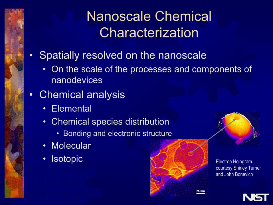
Nanoscale Chemical Characterization
• Spatially resolved on the nanoscale • On the scale of the processes and components of
nanodevices• Chemical analysis
• Elemental• Chemical species distribution
• Bonding and electronic structure
• Molecular• Isotopic Electron Hologram
courtesy Shirley Turner and John Bonevich

Measurement Research ApproachNo single “right” tool
Multiple techniques must be used;All techniques have severe limitations
• Probes• Photons, Ions, Electrons
• Spectroscopies• Optical, Mass
Spectrometry, X-ray, Electron
• Required Information• Molecular and/or• Elemental and/or• Isotopic • Spatial Resolution
• 1D, 2D, 3D
Approaches Analytical Needs

Imaging & Chemical Information• Atomic scale imaging
• Approaches:• Scanned Probes (STM, AFM)• Field Ion Microscope (Atom Probe)• High Resolution Transmission Electron Microscopy
• Takes advantage of broad spectrum “interaction”• Lacks specificity or requires specific sample
• Chemical Information• Requires spectroscopy• Inherently poorer signal to noise
• Selective interaction with very low cross section
• Chemical Imaging is MOST challenging

Drivers for Nanoscale Chemistry• Industrial needs:
• Current needs• Semiconductor
• Gate oxides, dopant levels, shrinking device dimensions• Optoelectronics• Nanoparticles/powders
• Catalysts, pigments, powder metallurgy, explosives, etc.• Coatings and Nanocomposites …
• Near future needs• Biomedical/Biotech• Microelectromechanical systems (MEMS)• Unknowns?
• Government needs:• Defense Department• Homeland Security• Biomedical - NIH

Example Need: Semiconductor Technology
Dimension (nm) Today 2014 Gate length 120 22
<20% <20%Equiv gate dielectric 1.9-1.5 0.5-0.6
<4% <4% Sidewall spacer 72-144 3.7-7.5
<10% <10%Silicide thickness 55 12Contact depth 75-145 15-35Drain extension depth 42-70 8-13Retrograde channel 21-35 4-8

Semiconductor Example
• Gate Dielectrics• Insulator controlling
electrical “shorts” in transistors
• Now only a few nanometers thick
• Chemically complex • Si to Si-O-N to Si-O to
Si
• Dopant Concentration & Location• A few atoms of B, P, As,
etc. control electrical properties
Poly-Si
Si-O-N
Si
2 nm
Courtesy of John Henry Scott

Gate Dielectric
• Variation of Si, O, N content along thickness of the gate is critical to electrical properties
• Must combine nanoscale structural and chemical information to understand the system
• Point analysis combined with morphology image
O
N
Si
Courtesy of
O
N
Si

Outline• What is and why do we need chemical
characterization and imaging?• Current state of the art
• 1 and 2 D• Why 2D is insufficient?
• What makes nanotechnology different• How do we do 3D?• What are the roadblocks?• Is it worth it?

Chemical Imaging 1D, 2D, 3D• One dimensional (point analysis related to
general (nonspectroscopic) imaging system) • Common, various resolutions, typically surface or
projection image• Manual or semiautomated
• Two dimensional (mapping)• Common, various resolutions, speeds• Automated
• Three dimensional• Not common in nanodevices• Common in medical imaging

2D Mapping Example
• Compositional Maps• Qualitative• Quantitative
• Solves many simple problems
• Complexity can be misinterpreted
• Analytical resolution can vary in x, y, z
Sm map Co map C map
Courtesy of John Henry Scott

Nanotech Measurement Challenge
Number of Atoms vs. SizeU3O8 Spheres
1.0E+00
1.0E+02
1.0E+04
1.0E+06
1.0E+08
1.0E+10
1.0E+12
1.0E+14
1.0E+16
1.0E+18
0.1 1 10 100 1000 10000 100000
Diameter in Nanometers
No.
of A
tom
s
Comfort zone for most analytical laboratories
New technology needed
Current research Incr
easi
ng S
ensi
tivity
Increasing Spatial Resolution

Why 2D is insufficient?What makes nanotechnology different
• Surface Images• Scanned Probes• Scanning Electron
Microscopes• Inherently 2D or shallow 3D
• Projection Images• Transmission Electron
Microscopes• Inherently 2D with 3D
convoluted• Chemical/Property Maps
• Inherently 2D• Diagrams for cases we
cannot image and measure • We use a lot of diagrams in
nanotechnology
Most Common Nanotech Images:
3 µm
Courtesy of John Henry Scott

• Determine the relationship of components within complex nanodevices
• Many device components are now smaller than our analytical volume
• 3D morphology is not enough
• Need micrometer scale with nanometer resolution
• Needed by current and future nanotechnologies
Why Nanoscale 3D Chemical Imaging?
3 µm
Which surface or projection?

Need for 3D Chemical ReconstructionProjection and Surface Images are Limiting
• Currently most used approach is 2D projection or surface morphologic imaging with limited chemical mapping
• This approach can easily lead to misinterpretation
• Chemical 3D information is now often required to determine true nature of working nanodevices and their failure modes Drawing by John O’Brien, The New Yorker Magazine (1991)

Outline• What is and why do we need chemical
characterization and imaging?• Current state of the art
• 1 and 2 D• Why 2D is insufficient?
• What makes nanotechnology different• How do we do 3D?• What are the roadblocks?• Is it worth it?

Current State-of-the-Art: 3D
• Current 3D nanoscale methods• X-ray tomography at beamlines for
morphology• Electron tomography for morphology• Energy Filtered Transmission Electron
Microscopy (EFTEM) tomography• Atom Probe • SPM• Confocal methods

Attaining 3D• Serial sectioning
• Ultramicrotomy – Biology • FIB – Materials • 2D mapping of each section (many
techniques)• Depth profiling
• Surface milling, ablation, or etching• 2D mapping over time (Atom Probe, SIMS,
FIB, Auger, XPS, etc.)• Tomography
• Tilt series with hyperspectral imaging

EFTEM(Energy Filtered TEM)
• Example of catalyst particles in zeolite
MCM 41 with catalyst nanoparticles, 35 degrees tilt, field of view ~150nm
From M.Weyland, P.A.Midgley and R.E Dunin-Borkowski
53 HAADF images acquired at 2 degree intervals from +60 to -48 degrees

Atom Probe• “Boils off” atoms at
surface and sends through imaging TOF MS, then recombines the many first surface images to reconstruct 3D chemical images
• Difficult sample preparation (even by TEM standards)
• Limited field of view• Conducting or
semiconductingsamples Courtesy of Imago
Cu - Red, Ag - Blue

Outline• What is and why do we need chemical
characterization and imaging?• Current state of the art
• 1 and 2 D• Why 2D is insufficient?
• What makes nanotechnology different• How do we do 3D?• What are the roadblocks?• Is it worth it?

• Improve probe• Increase Intensity
• Increase interaction with specimen
• Improve detectors• Change detector
efficiency
• Improve Probe• Reduce size
• Reduce interaction volume
• Improve environment• Reduce interference
Improve Sensitivity Increase Spatial Resolution
New technology is needed to break through this incompatibility
These two needs are often incompatible
Roadblocks to 3D Nano

Improving Spatial Resolution SIMS Cluster Ions
25 keV Ga+
Range = 4 nm
25 keVGa+
Range = 40 nm
25 keV C60+
Each C = 417 eVRange = 4 nm
0 PMMA 80 nm
Monoatomic primary ion bombardment creates extensive subsurface damage resulting in reduced sensitivity and no compositional depth information for organics and reduced depth resolution for elemental depth profiling.
Cluster ions offer:Lower penetration depthHigher sputter rateHigher secondary ion yieldsReduced accumulation of beam damage
SRIM Simulation of Ion Impacts on PMMA film-normal incidence
Courtesy of Greg Gillen

New X-ray Technology• Microcalorimeters
• Few eV resolution, multichannel
• Improves spectral resolution allowing chemical mapping
• Silicon Drift Detectors• Large area, high
count rate• Improves efficiency,
sensitivity, speed500 1000 1500 2000
0
500
1000
1500
2000
NIST µcal EDS
C Kα
O Kα
Fe LαNi Lα
Zn Lα
Mg KαAl Kα
Si Kα
µcal
ED
S C
ount
s (0.
16 e
V b
ins)
Energy (eV)
0
5000
10000
15000
(real-time analog processing)
NIST K3670 glass Si(Li) EDS
Si(L
i) ED
S Co
unts
(10
eV b
ins)
Courtesy of Dale Newbury

Improving Sensitivity & Spatial ResolutionImplemented New Technologies
• Mass Spectrometry (SIMS)• Order of magnitude improvement in depth
resolution• Electron Microscopy
• Several orders of magnitude improvement in electron beam current and X-ray collection efficiency
• Improved spatial resolution by factor of five or more• Optical Spectroscopy (NSOM)
• 10-50 time improvement in spatial resolution

3D Chemical Imagingwell positioned to move forward
but have major technical roadblocks• Higher Speed –
• At nm sized pixels a 1 X 1 µm area would take 1000pixels x 1000pixels x ~1sec = 12 days
• Higher Sensitivity • From 100’s of atoms to single atom• Zeptogram spectroscopy and analysis
• High resolution in x, y, and z• Larger volumes• Higher Spatial Precision
• Stages need atomic level precision in 6 axes• Insensitivity to environment• Better measurement environments
• Move from 1D and 2D to 3D• Spectroscopic nanotomography

Outline• What is and why do we need chemical
characterization and imaging?• Current state of the art
• 1 and 2 D• Why 2D is insufficient?
• What makes nanotechnology different• How do we do 3D?• What are the roadblocks?• Is it worth it?

3D Chemical Imaging• The holy grail of characterization and chemical
measurement:
• Know each atom and relationship to all others
• Where one or more atoms well placed or misplaced can make or break a nanodevice
Courtesy David Muller, Cornell

Metric UnitsMetric UnitsNameName SymbolSymbol
10241024 yottayotta YY10211021 zettazetta ZZ10181018 exaexa EE10151015 petapeta PP10121012 teratera TT109109 gigagiga GG106106 megamega MM103103 kilokilo kk102102 hectohecto hh101101 dekadeka dada
FactorFactor NameName SymbolSymbol10-110-1 decideci dd10-210-2 centicenti cc10-310-3 millimilli mm10-610-6 micromicro µµ10-910-9 nanonano nn10-1210-12 picopico pp10-1510-15 femtofemto ff10-1810-18 attoatto aa10-2110-21 zeptozepto zz10-2410-24 yoctoyocto yy
Nanotechnology requires zeptogram level chemical analysis