enhanced 8051 microcontroller with 10bit adc mcu/8bit flash mcu/ss481a_sh79f081b... · sh79f081b...
TRANSCRIPT

SH79F081B
Enhanced 8051 Microcontroller with 10bit ADC
1 V2.0
1. Features 8bits micro-controller with Pipe-line structured 8051
compatible instruction set Flash ROM: 8K Bytes RAM: internal 256 Bytes EEPROM-like: 2K Bytes Operation Voltage:
fOSC = 400k - 16MHz, VDD = 3.6V - 5.5V Oscillator (code option):
- Crystal oscillator: 400kHz - 16MHz - Ceramic oscillator: 400kHz - 16MHz - Internal RC: 12.3MHz/16MHz
26 CMOS bi-directional I/O pins Built-in pull-up resistor for input pin Three 16-bit timer/counters T0, T1and T2 One 12-bit PWM Two 8-bit PWM Powerful interrupt sources:
- Timer0, 1, 2 - INT0, 1 - INT40-43, INT45-46 - ADC, EUART, SPI, PWM, SCM
EUART SPI interface (Master/Slave Mode) 8channels 10-bits Analog Digital Converter (ADC),
with comparator function built-in Buzzer Low Voltage Reset (LVR) function (enabled by
code option) - LVR voltage level 1: 4.1V - LVR voltage level 2: 3.7V
CPU Machine cycle: 1 oscillator clock Watch Dog Timer (WDT) Warm-up Timer Support Low power operation modes:
- Idle Mode - Power-Down Mode
Flash Type Package:
- SOP28
2. General Description The SH79F081B is a high performance 8051 compatible micro-controller, regard to its build-in Pipe-line instruction fetch structure, that helps the SH79F081B can perform more fast operation speed and higher calculation performance, if compare SH79F081B with standard 8051 at same clock speed. The SH79F081B retains most features of the standard 8051. These features include internal 256 bytes RAM, EUART and Int0-3.In addition, the SH79F081B contains 8K bytes Flash memory block both for program and data. Also the ADC and PWM timer functions are incorporated in SH79F081B. For high reliability and low cost issues, the SH79F081B builds in Watchdog Timer, System Clock Monitor, and Low Voltage Reset function. And SH79F081B also supports two power saving modes to reduce power consumption.

SH79F081B
2
3. Block Diagram
8K BytesFlash ROM
Internal 256 BytesData RAM
Oscillator
Pipelined 8051 architecture
Timer0 (16bit)Timer1 (16bit)Timer2 (16bit)
Reset circuit RST
XTAL2
XTAL1
VDD
External Interrupt
Buzzer
Power
Watch Dog
12-bit PWM
InternalOscillator
8-bit PWM
8-bit PWM
Port 2 Configuration I/O
Port 1 Configuration I/O
P1.2 - P1.7
P2.0 - P2.7
P0.2 - P0.7
Port 3 Configuration I/O
P3.0 - P3.5
SPI
EUART
10-bit ADC
JTAG ports(for debug)
Port 0 Configuration I/O
SCM

SH79F081B
3
4. Pin Configuration 28 SOP
SH
79F081B
M
1
2
3
4
5
6
7
8
9
10
11
12
13
14
28
27
26
25
24
23
22
21
20
19
18
17
16
15
P2.6/INT45/PWM01
P2.7/INT46/PWM11
P0.7/INT1/PWM21
P2.3/PWM2
RST/P1.7
XTAL1/P3.4
XTAL2/P3.3
VDD
P2.4/PWM0
T2/INT0/P3.1
FLT/SS/P3.0
P3.5
P2.2/MOSI/RXD
P2.1/MISO/TXD
P2.0/SCK/BZ
P2.5/PWM1
T2EX/P3.2
T0/VREF/P1.6 P0.6/T1
P0.5/AN3
P0.3/AN1
P0.4/AN2
P0.2/AN0
VSS
TMS/INT42/AN5/P1.3
TDI/INT41/AN6/P1.4
TCK/INT40/AN7/P1.5
TDO/INT43/AN4/P1.2

SH79F081B
4
Table 4.1 Pin Function
Pin No. Pin Name Default Function
1 TDO/INT43/AN4/P1.2 P1.2
2 TMS/INT42/AN5/P1.3 P1.3
3 TDI/INT41/AN6/P1.4 P1.4
4 TCK/INT40/AN7/P1.5 P1.5
5 T0/P1.6 P1.6
6 RST————
/P1.7 Reset pin or P1.7 (code option)
9 VDD -----
10 VSS -----
8 XTAL1/P3.4 P3.4 or osc input pin (code option)
7 XTAL2/P3.3 P3.3 or osc output pin (code option)
11 T2EX/P3.2 P3.2
12 T2/INT0/P3.1 P3.1
13 FLT/SS———
/P3.0 P3.0
14 P3.5 P3.5
15 BZ/SCK/P2.0 P2.0
16 TXD/MISO/P2.1 P2.1
17 RXD/MOSI/P2.2 P2.2
18 PWM2/P2.3 P2.3
19 PWM0/P2.4 P2.4
22 PWM1/P2.5 P2.5
21 PWM01/INT45/P2.6 P2.6
20 PWM11/INT46/P2.7 P2.7
23 PWM21/INT1/P0.7 P0.7
24 T1/P0.6 P0.6
*25 AN3/P0.5 P0.5
*26 AN2/P0.4 P0.4
*27 AN1/P0.3 P0.3
*28 AN0/P0.2 P0.2
*Note: (1) P0.2, P0.3, P0.4, P0.5 are configured as N-channel open drain I/O (2) The out most pin function has the highest priority, and the inner most pin function has the lowest priority (Refer to Pin
Configuration Diagram. This means when one pin is occupied by a higher priority function (if enabled) cannot be used as the lower priority functional pin, even when the lower priority function is also enabled. Until the higher priority function is closed by software, can the corresponding pin be released for the lower priority function use.

SH79F081B
5
5. Pin Description
Pin No. Type Description
I/O PORT P0.2 - P0.7 I/O 6 bit General purpose CMOS I/O P1.2 - P1.7 I/O 6 bit General purpose CMOS I/O P2.0 - P2.7 I/O 8 bit General purpose CMOS I/O P3.0 - P3.5 I/O 6 bit General purpose CMOS I/O
Timer T0 I/O Timer0 external input/Comparator output T1 I/O Timer1 external input/Comparator output T2 I/O Timer2 external input/ Baud-Rate generator
T2EX I Timer 2 Reload/Capture/Direction Control PWM
PWM0 O Output pin for 12-bit PWM timer PWM1 O Output pin for 8-bit PWM timer PWM2 O Output pin for 8-bit PWM timer
PWM01 O Output pin for 12-bit PWM timer with fixed phase relationship of PWM0 PWM11 O Output pin for 8-bit PWM timer with fixed phase relationship of PWM1 PWM21 O Output pin for 8-bit PWM timer with fixed phase relationship of PWM2
FLT I PWM Fault Detect input
EUART
RXD I EUART data input TXD O EUART data output
SPI MOSI I/O SPI master output slave input MISO I/O SPI master input slave output SCK I/O SPI serial clock
SS———
I SPI Slave Select
ADC AN0 - AN7 I ADC input channel
AVREF I External ADC reference voltage input
Interrupt & Reset & Clock & Power INT0 - INT1 I External interrupt 0-1 input source
INT40 - INT43 INT45 - INT46 I External interrupt 40-43, 45-46 input source
RST————
I The device will be reset by A low voltage on this pin longer than 10us, an internal resistor about 100kΩ to VDD, So using only an external capacitor to GND can cause a power-on reset.
XTAL1 I Oscillator input XTAL2 O Oscillator output
VSS P Ground VDD P Power supply (3.6 - 5.5V)
(to be continued)

SH79F081B
6
(continue)
Pin No. Type Description
Buzzer BUZCON O Buzzer output pin
Programmer TDO (P1.2) O Debug interface: Test data out TMS (P1.3) I Debug interface: Test mode select TDI (P1.4) I Debug interface: Test data in TCK (P1.5) I Debug interface: Test clock in
Note: When P1.2-1.5 used as debug interface, functions of P1.2-1.5 are blocked.

SH79F081B
7
6. SFR Mapping The SH79F081B provides 256 bytes of internal RAM to contain general-purpose data memory and Special Function Register (SFR). The SFR of the SH79F081B fall into the following categories: CPU Core Registers: ACC, B, PSW, SP, DPL, DPH
Enhanced CPU Core Registers: AUXC, DPL1, DPH1, INSCON, XPAGE
Power and Clock Control Registers: PCON, SUSLO
Flash Registers: IB_OFFSET, IB_DATA, IB_CON1, IB_CON2, IB_CON3, IB_CON4, IB_CON5, FLASHCON
Data Memory Register: XPAGE
Hardware Watchdog Timer Registers: RSTSTAT
System Clock Control Register: CLKCON, SCMCON
Interrupt System Registers: IEN0, IEN1, IENC, IPH0, IPL0, IPH1, IPL1, EXF0, EXF1
I/O Port Registers: P0, P1, P2, P3, P0CR, P1CR, P2CR, P3CR, P0PCR, P1PCR, P2PCR, P3PCR, P0OS
Timer Registers: TCON, TMOD, TH0, TH1, TL0, TL1, T2CON, T2MOD, TH2, TL2, RCAP2L, RCAP2H, TCON1
EUART Registers: SCON, SBUF, SADEN, SADDR, PCON, RXDCON
SPI Registers: SPCON, SPSTA, SPDAT
ADC Registers: ADCON, ADT, ADCH, ADDL, ADDH
Buzzer Registers: BUZCON
PWM Registers: PWMEN, PWMLO, PWM0C, PWM0PL, PWM0PH, PWM0DL, PWM0DH, PWM1C, PWM1P, PWM1D, PWM2C, PWM2P, PWM2D, PWM0DT, PWM1DT, PWM2DT

SH79F081B
8
Table 6.1 CPU Core SFRs
Mnem Add Name POR/WDT/LVR /PIN Reset Value Bit7 Bit6 Bit5 Bit4 Bit3 Bit2 Bit1 Bit0
ACC E0H Accumulator 00000000 ACC.7 ACC.6 ACC.5 ACC.4 ACC.3 ACC.2 ACC.1 ACC.0
B F0H B Register 00000000 B.7 B.6 B.5 B.4 B.3 B.2 B.1 B.0
AUXC F1H C Register 00000000 C.7 C.6 C.5 C.4 C.3 C.2 C.1 C.0
PSW D0H Program Status Word 00000000 CY AC F0 RS1 RS0 OV F1 P
SP 81H Stack Pointer 00000111 SP.7 SP.6 SP.5 SP.4 SP.3 SP.2 SP.1 SP.0
DPL 82H Data Pointer Low byte 00000000 DPL0.7 DPL0.6 DPL0.5 DPL0.4 DPL0.3 DPL0.2 DPL0.1 DPL0.0
DPH 83H Data Pointer High byte 00000000 DPH0.7 DPH0.6 DPH0.5 DPH0.4 DPH0.3 DPH0.2 DPH0.1 DPH0.0
DPL1 84H Data Pointer 1 Low byte 00000000 DPL1.7 DPL1.6 DPL1.5 DPL1.4 DPL1.3 DPL1.2 DPL1.1 DPL1.0
DPH1 85H Data Pointer 1 High byte 00000000 DPH1.7 DPH1.6 DPH1.5 DPH1.4 DPH1.3 DPH1.2 DPH1.1 DPH1.0
INSCON 86H Data pointer select ----00-0 - - - - DIV MUL - DPS
Table 6.2 Power and Clock control SFRs
Mnem Add Name POR/WDT/LVR /PIN Reset Value Bit7 Bit6 Bit5 Bit4 Bit3 Bit2 Bit1 Bit0
PCON 87H Power Control 00--0000 SMOD SSTAT - - GF1 GF0 PD IDL
SUSLO 8EH Suspend Mode Control 00000000 SUSLO.7 SUSLO.6 SUSLO.5 SUSLO.4 SUSLO.3 SUSLO.2 SUSLO.1 SUSLO.0
Table 6.3 Flash control SFRs
Mnem Add Name POR/WDT/LVR /PIN Reset Value Bit7 Bit6 Bit5 Bit4 Bit3 Bit2 Bit1 Bit0
IB_OFF SET FBH Low byte offset of flash memory 00000000 IB_OFF
SET.7 IB_OFF SET.6
IB_OFF SET.5
IB_OFF SET.4
IB_OFF SET.3
IB_OFF SET.2
IB_OFF SET.1
IB_OFF SET.0
IB_DATA FCH Data Register for programming flash memory 00000000 IB_DATA.7 IB_DATA.6 IB_DATA.5 IB_DATA.4 IB_DATA.3 IB_DATA.2 IB_DATA.1 IB_DATA.0
IB_CON1 F2H Flash Memory Control Register 1 00000000 IB_CON1.7 IB_CON1.6 IB_CON1.5 IB_CON1.4 IB_CON1.3 IB_CON1.2 IB_CON1.1 IB_CON1.0
IB_CON2 F3H Flash Memory Control Register 2 ----0000 - - - - IB_CON2.3 IB_CON2.2 IB_CON2.1 IB_CON2.0
IB_CON3 F4H Flash Memory Control Register 3 ----0000 - - - - IB_CON3.3 IB_CON3.2 IB_CON3.1 IB_CON3.0
IB_CON4 F5H Flash Memory Control Register 4 ----0000 - - - - IB_CON4.3 IB_CON4.2 IB_CON4.1 IB_CON4.0
IB_CON5 F6H Flash Memory Control Register 5 ----0000 - - - - IB_CON5.3 IB_CON5.2 IB_CON5.1 IB_CON5.0
XPAGE F7H Memory Page 00000000 XPAGE.7 XPAGE.6 XPAGE.5 XPAGE.4 XPAGE.3 XPAGE.2 XPAGE.1 XPAGE.0
FLASHCON A7H Flash access control -------0 - - - - - - - FAC

SH79F081B
9
Table 6.4 WDT SFR
Mnem Add Name POR/WDT/LVR /PIN Reset Value Bit7 Bit6 Bit5 Bit4 Bit3 Bit2 Bit1 Bit0
RSTSTAT B1h Watchdog Timer Control *-***000 WDOF - PORF LVRF CLRF WDT.2 WDT.1 WDT.0
*Note: RSTSTAT initial value is determined by different RESET.
Table 6.5 CLKCON SFR
Mnem Add Name POR/WDT/LVR /PIN Reset Value Bit7 Bit6 Bit5 Bit4 Bit3 Bit2 Bit1 Bit0
CLKCON B2H System Clock Control Register -000---- - CLKS1 CLKS0 SCMIF - - - -
SCMCON A1H SCM Clock Control Register ------00 - - - - - - SCK1 SCK0
Table 6.6 Interrupt SFRs
Mnem Add Name POR/WDT/LVR /PIN Reset Value Bit7 Bit6 Bit5 Bit4 Bit3 Bit2 Bit1 Bit0
IEN0 A8H Interrupt Enable Control 0 00000000 EA EADC ET2 ES ET1 EX1 ET0 EX0
IEN1 A9H Interrupt Enable Control 1 -00-0--0 - ESCM EPWM - EX4 - - ESPI
IENC BAH Interrupt 4channel enable control 00000000 EXS47 EXS46 EXS45 EXS44 EXS43 EXS42 EXS41 EXS40
IPH0 B4H Interrupt Priority Control High 0 -0000000 - PADCH PT2H PSH PT1H PX1H PT0H PX0H
IPL0 B8H Interrupt Priority Control Low 0 -0000000 - PADCL PT2L PSL PT1L PX1L PT0L PX0L IPH
1 B5H Interrupt Priority Control High 1 -00-0--0 - PSCMH PPWMH - PX4H - - PSPIH
IPL1 B9H Interrupt Priority Control Low 1 -00-0--0 - PSCML PPWML - PX4L - - PSPIL E
XF0 8H External interrupt Control 0 00------ IT4.1 IT4.0 - - - - - -
EXF1 D8h External interrupt Control 1 -00-0000 - IF46 IF45 - IF43 IF42 IF41 IF40

SH79F081B
10
Table 6.7 Port SFRs
Mnem Add Name POR/WDT/LVR /PIN Reset Value Bit7 Bit6 Bit5 Bit4 Bit3 Bit2 Bit1 Bit0
P0 80H 6-bit Port 0 000000-- P0.7 P0.6 P0.5 P0.4 P0.3 P0.2 - -
P1 90H 6-bit Port 1 000000-- P1.7 P1.6 P1.5 P1.4 P1.3 P1.2 - -
P2 A0H 8-bit Port 2 00000000 P2.7 P2.6 P2.5 P2.4 P2.3 P2.2 P2.1 P2.0
P3 B0H 6-bit Port 3 --000000 - - P3.5 P3.4 P3.3 P3.2 P3.1 P3.0
P0CR E1H Port0 input/output direction control 000000-- P0CR.7 P0CR.6 P0CR.5 P0CR.4 P0CR.3 P0CR.2 - -
P1CR E2H Port1 input/output direction control 000000-- P1CR.7 P1CR.6 P1CR.5 P1CR.4 P1CR.3 P1CR.2 - -
P2CR E3H Port2 input/output direction control 00000000 P2CR.7 P2CR.6 P2CR.5 P2CR.4 P2CR.3 P2CR.2 P2CR.1 P2CR.0
P3CR E4H Port3 input/output direction control --000000 - - P3CR.5 P3CR.4 P3CR.3 P3CR.2 P3CR.1 P3CR.0
P0PCR E9H Internal pull-high enable for Port0 000000-- P0PCR.7 P0PCR.6 P0PCR.5 P0PCR.4 P0PCR.3 P0PCR.2 - -
P1PCR EAH Internal pull-high enable for Port1 000000-- P1PCR.7 P1PCR.6 P1PCR.5 P1PCR.4 P1PCR.3 P1PCR.2 - -
P2PCR EBH Internal pull-high enable for Port2 00000000 P2PCR.7 P2PCR.6 P2PCR.5 P2PCR.4 P2PCR.3 P2PCR.2 P2PCR.1 P2PCR.0
P3PCR ECH Internal pull-high enable for Port3 --000000 - - P3PCR.5 P3PCR.4 P3PCR.3 P3PCR.2 P3PCR.1 P3PCR.0
P0OS EFH Output mode control --0000-- - - P05OS P04OS P03OS P02OS - -
Table 6.8 Timer SFRs
Mnem Add Name POR/WDT/LVR /PIN Reset Value Bit7 Bit6 Bit5 Bit4 Bit3 Bit2 Bit1 Bit0
TCON 88H Timer/Counter0/1 Control 00000000 TF1 TR1 TF0 TR0 IE1 IT1 IE0 IT0
TMOD 89H Timer/Counter 0/1 Mode 00000000 GATE1 C/ T1———
M11 M10 GATE0 C/ T0———
M01 M00
TL0 8AH Timer/Counter 0 Low Byte 00000000 TL0.7 TL0.6 TL0.5 TL0.4 TL0.3 TL0.2 TL0.1 TL0.0
TH0 8CH Timer/Counter 0 High Byte 00000000 TH0.7 TH0.6 TH0.5 TH0.4 TH0.3 TH0.2 TH0.1 TH0.0
TL1 8BH Timer/Counter 1 Low Byte 00000000 TL1.7 TL1.6 TL1.5 TL1.4 TL1.3 TL1.2 TL1.1 TL1.1
TH1 8DH Timer/Counter 1 High Byte 00000000 TH1.7 TH1.6 TH1.5 TH1.4 TH1.3 TH1.2 TH1.1 TH1.1
T2CON C8H Timer/Counter 2 Control 00000000 TF2 EXF2 RCLK TCLK EXEN2 TR2 C/ T2———
CP/RL2
T2MOD C9H Timer/Counter 2 Control 0-----00 TCLKP2 - - - - - T2OE DCEN
RCAP2L CAH Timer/Counter 2 Reload /Capture Low Byte 00000000 RCAP2L.7 RCAP2L.6 RCAP2L.5 RCAP2L.4 RCAP2L.3 RCAP2L.2 RCAP2L.1 RCAP2L.0
RCAP2H CBH Timer/Counter 2 Reload /Capture High Byte 00000000 RCAP2H.7 RCAP2H.6 RCAP2H.5 RCAP2H.4 RCAP2H.3 RCAP2H.2 RCAP2H.1 RCAP2H.0
TL2 CCH Timer/Counter 4 Control 00000000 TL2.7 TL2.6 TL2.5 TL2.4 TL2.3 TL2.2 TL2.1 TL2.0
TH2 CDH Timer/Counter 4 Low Byte 00000000 TH2.7 TH2.6 TH2.5 TH2.4 TH2.3 TH2.2 TH2.1 TH2.0 TCON1 CEH Timer/Counter 4 High Byte ----0000 - - - - TCLKP1 TCLKP0 TC1 TC0

SH79F081B
11
Table 6.9 EUART SFRs
Mnem Add Name POR/WDT/LVR /PIN Reset Value Bit7 Bit6 Bit5 Bit4 Bit3 Bit2 Bit1 Bit0
SCON 98H Serial Control 00000000 SM0/FE SM1/RXOV SM2/TXCOL REN TB8 RB8 TI RI
SBUF 99H Serial Data Buffer 00000000 SBUF.7 SBUF.6 SBUF.5 SBUF.4 SBUF.3 SBUF.2 SBUF.1 SBUF.0 SADEN
9B
Slave Address Mask 00000000 SADEN.7 SADEN.6 SADEN.5 SADEN.4 SADEN.3 SADEN.2 SADEN.1 SADEN.0 SADDR
9A
Slave Address 00000000 SADDR.7 SADDR.6 SADDR.5 SADDR.4 SADDR.3 SADDR.2 SADDR.1 SADDR.0 PCON
87
Power & serial Control 00--0000 SMOD
SSTAT
- - GF1 GF0 PD IDL RXDCO
9F
RXD Schmidt Level Control 0------0 REFC - - - - - - RXDCON0
Table 6.10 SPI SFRs
Mnem Add Name POR/WDT/LVR /PIN Reset Value Bit7 Bit6 Bit5 Bit4 Bit3 Bit2 Bit1 Bit0
SPCON A2H SPI control register 00000000 DIR MSTR CPHA CPOL SSDIS SPR2 SPR1 SPR0
SPSTA F8H SPI status register 00000--- SPEN SPIF MODF WCOL RXOV - - -
SPDAT A3H SPI data register 00000000 SPD.7 SPD.6 SPD.5 SPD.4 SPD.3 SPD.2 SPD.1 SPD.0
Table 6.11 ADC SFRs
Mnem Add Name POR/WDT/LVR /PIN Reset Value Bit7 Bit6 Bit5 Bit4 Bit3 Bit2 Bit1 Bit0
ADCON 93H ADC Control 000-0000 ADON ADCIF EC - SCH2 SCH1 SCH0 GO/
DONE
ADT 94H ADC Time Configuration 000-0000 TADC2 TADC1 TADC0 - TS3 TS2 TS1 TS0
ADCH 95H ADC Channel Configuration 00000000 CH7 CH6 CH5 CH4 CH3 CH2 CH1 CH0
ADDL 96H ADC Data Low Byte ------00 - - - - - - A1 A0
ADDH 97H ADC Data High Byte 00000000 A9 A8 A7 A6 A5 A4 A3 A2
Table 6.12 Buzzer SFR
Mnem Add Name POR/WDT/LVR /PIN Reset Value Bit7 Bit6 Bit5 Bit4 Bit3 Bit2 Bit1 Bit0
BUZCON BDH Buzzer output control ---00000 - - - BCA3 BCA2 BCA1 BCA0 BZEN

SH79F081B
12
Table 6.13 PWM SFRs
Mnem Add Name POR/WDT/LVR /PIN Reset Value Bit7 Bit6 Bit5 Bit4 Bit3 Bit2 Bit1 Bit0
PWMEN CFH PWM timer enable -0000000 - EFLT EPWM21 EPWM11 EPWM01 EPWM2 EPWM1 EPWM0
PWMLO E7H PWM register Lock 00000000 PWMLO.7 PWMLO.6 PWMLO.5 PWMLO.4 PWMLO.3 PWMLO.2 PWMLO.1 PWMLO.0
PWM0C D2H 12-bit PWM Control 00-00000 PWM0IE PWM0IF - FLTS FLTC PWM0S TnCK01 TnCK00
PWM0PL D3H 12-bit PWM Period Control low byte 00000000 PP0.7 PP0.6 PP0.5 PP.4 PP0.3 PP0.2 PP0.1 PP0.0
PWM0PH D4H 12-bit PWM Period Control high byte ----0000 - - - - PP0.11 PP0.10 PP0.9 PP0.8
PWM0DL D5H 12-bit PWM Duty Control low byte 00000000 PD0.7 PD0.6 PD0.5 PD0.4 PD0.3 PD0.2 PD0.1 PD0.0
PWM0DH D6H 12-bit PWM Duty Control high byte ----0000 - - - - PD0.11 PD0.10 PD0.9 PD0.8
PWM1C D9H 8-bit PWM1 Control 00---000 PWM1IE PWM1IF - - - PWM1S TnCK11 TnCK10
PWM1P DAH 8-bit PWM1 Period Control 00000000 PP1.7 PP1.6 PP1.5 PP1.4 PP1.3 PP1.2 PP1.1 PP1.0
PWM1D DBH 8-bit PWM1 Duty Control 00000000 PD1.7 PD1.6 PD1.5 PD1.4 PD1.3 PD1.2 PD1.1 PD1.0
PWM2C DDH 8-bit PWM2 Control 00---000 PWM2IE PWM2IF - - - PWM2S TnCK21 TnCK20
PWM2P DEH 8-bit PWM2 Period Control 00000000 PP2.7 PP2.6 PP2.5 PP2.4 PP2.3 PP2.2 PP2.1 PP2.0
PWM2D DFH 8-bit PWM2 Duty Control 00000000 PD2.7 PD2.6 PD2.5 PD2.4 PD2.3 PD2.2 PD2.1 PD2.0
PWM0DT D1H PWM01 Dead time control 00000000 DT0.7 DT0.6 DT0.5 DT0.4 DT0.3 DT0.2 DT0.1 DT0.0
PWM1DT D7H PWM11 Dead time control 00000000 DT1.7 DT1.6 DT1.5 DT1.4 DT1.3 DT1.2 DT1.1 DT1.0
PWM2DT DCH PWM21 Dead time control 00000000 DT2.7 DT2.6 DT2.5 DT2.4 DT2.3 DT2.2 DT2.1 DT2.0
Note: - :Unimplemented

SH79F081B
13
SFR Map
Bit
addressable Non Bit addressable
0/8 1/9 2/A 3/B 4/C 5/D 6/E 7/F
F8H SPSTA IB_OFFSET IB_DATA FFH
F0H B AUXC IB_CON1 IB_CON2 IB_CON3 IB_CON4 IB_CON5 XPAGE F7H
E8H EXF0 P0PCR P1PCR P2PCR P3PCR P0OS EFH
E0H ACC P0CR P1CR P2CR P3CR PWMLO E7H
D8H EXF1 PWM1C PWM1P PWM1D PWM2DT PWM2C PWM2P PWM2D DFH
D0H PSW PWM0DT PWM0C PWM0PL PWM0PH PWM0DL PWM0DH PWM1DT D7H
C8H T2CON T2MOD RCAP2L RCAP2H TL2 TH2 TCON1 PWMEN CFH
C0H C7H
B8H IPL0 IPL1 IENC BUZCON BFH
B0H P3 RSTSTAT CLKCON IPH0 IPH1 B7H
A8H IEN0 IEN1 AFH
A0H P2 SCMCON SPCON SPDAT FLASHCON A7H
98H SCON SBUF SADDR SADEN RXDCON 9FH
90H P1 ADCON ADT ADCH ADDL ADDH 97H
88H TCON TMOD TL0 TL1 TH0 TH1 SUSLO 8FH
80H P0 SP DPL DPH DPL1 DPH1 INSCON PCON 87H
0/8 1/9 2/A 3/B 4/C 5/D 6/E 7/F
Note: The unused addresses of SFR are not available.

SH79F081B
14
7. Normal Function 7.1 CPU 7.1.1 CPU Core SFR Feature
CPU core registers: ACC, B, PSW, SP, DPL, DPH Accumulator ACC is the Accumulator register. The mnemonics for accumulator-specific instructions, however, refer to the Accumulator simply as A. B Register The B register is used during multiply and divide operations. For other instructions it can be treated as another scratch pad register. Stack Pointer (SP) The Stack Pointer Register is 8 bits wide, It is incremented before data is stored during PUSH, CALL executions and it is decremented after data is out of stack during POP, RET, RETI executions. The stack may reside anywhere in on-chip internal RAM (00H-FFH). On reset, the Stack Pointer is initialized to 07H causing the stack to begin at location 08H. Program Status Word Register (PSW) The PSW register contains program status information. Table 7.1 PSW Register
D0H 第7位 第6位 第5位 第4位 第3位 第2位 第1位 第0位 PSW CY AC F0 RS1 RS0 OV F1 P R/W R/W R/W R/W R/W R/W R/W R/W R
Reset Value (POR/WDT/LVR/PIN) 0 0 0 0 0 0 0 0
Bit Number Bit Mnemonic Description
7 CY Carry flag bit
0: no carry or borrow in an arithmetic or logic operation 1: a carry or borrow in an arithmetic or logic operation
6 AC Auxiliary Carry flag bit
0: an auxiliary carry or borrow in an arithmetic or logic operation 1: an auxiliary carry or borrow in an arithmetic or logic operation
5 F0 F0 flag bit Available to the user for general purposes
4-3 RS[1:0]
R0-R7 Register bank select bits 00: Bank0 (Address to 00H-07H) 01: Bank1 (Address to 08H-0FH) 10: Bank2 (Address to 10H-17H) 11: Bank3 (Address to 18H-1FH)
2 OV Overflow flag bit
0: no overflow happen 1: an overflow happen
1 F1 F1 flag bit Available to the user for general purposes
0 P Parity flag bit
0: an even number of “one” bits in the Accumulator 1: an odd number of “one” bits in the Accumulator
Data Pointer Register (DPTR) DPTR consists of a high byte (DPH) and a low byte (DPL). Its intended function is to hold a 16-bit address, but it may be manipulated as a 16-bit register or as two independent 8-bit registers.

SH79F081B
15
7.1.2 Enhanced CPU core SFRs
Extended 'MUL' and 'DIV' instructions: 16bit*8bit, 16bit/8bit Dual Data Pointer Enhanced CPU core registers: AUXC, DPL1, DPH1, INSCON
The SH79F081B has modified 'MUL' and 'DIV' instructions. These instructions support 16 bit operand. A new register - the register is applied to hold the upper part of the operand/result. The AUXC register is used during 16 bit operand multiply and divide operations. For other instructions it can be treated as another scratch pad register. After reset, the CPU is in standard mode, which means that the 'MUL' and 'DIV' instructions are operating like the standard 8051 instructions. To enable the 16 bit mode operation, the corresponding enable bit in the INSCON register must be set.
Operation Result A B AUXC
MUL INSCON.2 = 0; 8 bit mode (A)*(B) Low Byte High Byte ---
INSCON.2 = 1; 16 bit mode (AUXC A)*(B) Low Byte Middle Byte High Byte
DIV INSCON.3 = 0; 8 bit mode (A)/(B) Quotient Low Byte Remainder ---
INSCON.3 = 1; 16 bit mode (AUXC A)/(B) Quotient Low Byte Remainder Quotient High Byte
Dual Data Pointer Using two data pointers can accelerate data memory moves. The standard data pointer is called DPTR and the new data pointer is called DPTR1. DPTR1 is the same with DPTR, which consists of a high byte (DPH1) and a low byte (DPL1). Its intended function is to hold a 16-bit address, but it may be manipulated as a 16-bit register or as two independent 8-bit registers. The DPS bit in INSTCON register is used to choose the active pointer. The user can switch data pointers by toggling the DPS bit. And all DPTR-related instructions will use the currently selected data pointer. Register Table 7.2 Data Pointer Select Register
86H Bit7 Bit6 Bit5 Bit4 Bit3 Bit2 Bit1 Bit0 INSCON - - - - DIV MUL - DPS
R/W - - - - R/W R/W - R/W
Reset Value (POR/WDT/LVR/PIN) - - - - 0 0 - 0
Bit Number Bit Mnemonic Description
3 DIV 16 bit/8 bit Divide Selection Bit
0: 8 bit Divide 1: 16 bit Divide
2 MUL 16 bit/8 bit Multiply Selection Bit
0: 8 bit Multiply 1: 16 bit Multiply
0 DPS Data Pointer Selection Bit
0: Data pointer 1: Data pointer1

SH79F081B
16
7.2 RAM SH79F081B provides internal RAM for random data storage. The internal data memory is mapped into four separated segments:
The Lower 128 bytes of RAM (addresses 00H to 7FH) are directly and indirectly addressable. The Upper 128 bytes of RAM (addresses 80H to FFH) are indirectly addressable only. The Special Function Registers (SFR, addresses 80H to FFH) are directly addressable only.
The Upper 128 bytes occupy the same address space as SFR, but they are physically separate from SFR space. When an instruction accesses an internal location above address 7FH, the CPU can distinguish whether to access the upper 128 bytes data RAM or to access SFR by different addressing mode of the instruction. Note: the unused address is unavailable in SFR.
7FH
80H
0FFH 0FFH
80H
00
Upper128 bytesInternal
Ramindirect
accesses
Lower128 bytesInternal
Ramdirect or indirect
accesses
SpecialFunctionRegister
direct accesses
The Internal and External RAM Configuration

SH79F081B
17
7.3 Flash Program Memory 7.3.1 Features
The program memory consists 8 X 1KB sectors, total 8KB 2K EEPROM-like Programming and erase can be done over the full operation voltage range Write, read and erase operation are all supported by In-Circuit Programming (ICP) Fast mass/sector erase and programming Minimum program/erase cycles: 100,000 Minimum years data retention: 10 Low power consumption
EEPROM Like Data Block
Program Memory Block
0000H0000H
0800H
Information Block
FFFFH
Program Memory Block
2000H(8K)
Reserved(no use)
The SH79F081B embeds 8K flash program memory for program code. The flash program memory provides electrical erasure and programming and supports In-Circuit Programming (ICP) mode and Self-Sector Programming (SSP) mode. The SH79F081B also embeds 2048 bytes EEPROM-like memory block for storing user data. Each sector is 256 bytes. It has 8 sectors. Flash operation defined: In-Circuit Programming (ICP): Through the Flash programmer to wipe the Flash memory, read and write operations. Self-Sector Programming (SSP) mode: User Program code runs in Program Memory to wipe the Flash memory, read and write operations.
The ICP mode supports the following operations: (1) Code-Protect Control mode Programming
SH79F081B code protection function provides a high-performance security measures for the user. Each partition has four modes are available. Code protection mode 0: allow/forbid any programmer write/read operations (not including overall erasure). Code protection mode 1: allow/forbid through MOVC instructions to read operation in other sectors, or through SSP mode
to erased/write operation. The user must use the following two ways to complete code protection control mode Settings: 1. Flash programmer in ICP mode is set to corresponding protection bit to enter the protected mode. 2. The SSP mode does not support code protection control mode programming.

SH79F081B
18
(2) Mass Erase
Regardless of the state of the code protection control mode, the overall erasure operation will erase all programs, code options, the code protection bit, but they will not erase EEPROM-like memory block. The user must use the following way to complete the overall erasure: Flash programmer in ICP mode sends overall erasure instruction to run overall erasure. The SSP mode does not support overall erasure mode.
(3) Sector Erase Sector erasure operations will erase the content of selected sector. The user program (SSP) and Flash programmer can perform this operation. For user programs to perform the operation, code protection mode 1 in the selected sector must be forbidden. For Flash programmer to perform the operation, code protection mode 0 in the selected sector must be forbidden. The user must use one of the following two ways to complete sector erasure: 1. Flash programmer in ICP mode send sector erasure instruction to run sector erasure. 2. Through the SSP function sends sector erasure instruction to run sector erasure (see chapter SSP).
(4) EEPROM-Like Erase EEPROM-like memory block erasure operations will erase the content in EEPROM-like memory block. The user program (SSP) and Flash programmer can perform this operation. The user must use one of the following two ways to complete EEPROM-like memory block erasure: 1. Flash programmer in ICP mode sends EEPROM-like memory block erasure instruction to run EEPROM-like memory
block erasure. 2. Through the SSP function send EEPROM-like memory block erasure instruction to run EEPROM-like memory block
erasure (see chapter SSP). (5) Write/Read Code
Write/read code operation can read or write code from flash memory block. The user program (SSP) and Flash programmer can perform this operation. For user programs to perform the operation, code protection mode 1 in the selected sector must be forbidden. Regardless of the security bit Settings or not, the user program can read/write the sector which contains program itself. For Flash programmer to perform the operation, code protection mode 0 in the selected sector must be forbidden. The user must use one of the following two ways to complete write/read code: 1. Flash programmer in ICP mode send write/read code instruction to run write/read code. 2. Through the SSP function send write/read code instruction to run write/read code.
(6) Write/Read EEPROM-Like EEPROM-like memory block operation can read or write data from EEPROM-like memory block. The user program (SSP) and Flash programmer can perform this operation. The user must use one of the following two ways to complete write/read EEPROM-like memory block: 1. Flash programmer in ICP mode send write/read EEPROM-like memory block instruction to run write/read EEPROM-like
memory block. 2. Through the SSP function send write/read EEPROM-like memory block instruction to run write/read EEPROM-like
memory block.
Operation SSP ICP
Code Protection non support support
Sector Erase support (without security bit)
support (without security bit)
Mass Erase non support support
EEPROM-like Erase support support
Write/Read support (without security bit or its own sector)
support (without security bit)
EEPROM-like Write/Read support support

SH79F081B
19
7.3.2 Flash Operation in ICP Mode ICP mode is performed without removing the micro-controller from the system. In ICP mode, the user system must be power-off, and the programmer can refresh the program memory through ICP programming interface. The ICP programming interface consists of 6 wires (VDD, GND, TCK, TDI, TMS, and TDO). At first the four JTAG pins (TDO, TDI, TCK, and TMS) are used to enter the programming mode. Only after the three pins are inputted the specified waveform, the CPU will enter the programming mode. For more detail description please refers to the FLASH Programmer’s user guide. In ICP mode, all the flash operations are completed by the programmer through 6-wire interface. Since the program timing is very sensitive, five jumpers are needed (VDD, TDO, TDI, TCK, TMS) to separate the program pins from the application circuit as the following diagram.
MCU
TCK
TDI
TDOGND
To ApplicationCircuit
Jumper
FlashProgrammer
VDD
TMS
The recommended steps are as following: (1) The jumpers must be open to separate the programming pins from the application circuit before programming. (2) Connect the programming interface with programmer and begin programming. (3) Disconnect programmer and short these jumpers after programming is complete.

SH79F081B
20
7.4 SSP Function The SH79F081B provides SSP (Self Sector Programming) function, each sector can be sector erased (except the last sector, sector 15) or programmed by the user’s code if the selected sector is not be protected. But once sector has been programmed, it cannot be reprogrammed before sector erase. The SH79F081B builds in a complex control flow to prevent the code from carelessly modification. If the dedicated conditions are not met (IB_CON2-5), the SSP will be terminated. 7.4.1 SSP Register
Table 7.3 Offset Register for Programming
F7H Bit7 Bit6 Bit5 Bit4 Bit3 Bit2 Bit1 Bit0 XPAGE XPAGE.7 XPAGE.6 XPAGE.5 XPAGE.4 XPAGE.3 XPAGE.2 XPAGE.1 XPAGE.0
R/W R/W R/W R/W R/W R/W R/W R/W R/W
Reset Value (POR/WDT/LVR/PIN) 0 0 0 0 0 0 0 0
Flash memory, one sector is 1024 bytes
Bit Number Bit Mnemonic Description 7-2 XPAGE[7:2] Sector of the flash memory to be programmed, 000000---means sector 0, and so on
1-0 XPAGE[1:0] High Address of Offset of the flash memory sector to be programmed
EEPROM-like memory, one sector is 256 bytes
Bit Number Bit Mnemonic Description 7-3 XPAGE[7:3] reserved
2-0 XPAGE[2:0] Sector of the flash memory to be programmed, 000---means sector 0, and so on
Table 7.4 Offset of Flash Memory for Programming
FBH Bit7 Bit6 Bit5 Bit4 Bit3 Bit2 Bit1 Bit0
IB_OFFSET IB_OFF SET.7
IB_OFF SET.6
IB_OFF SET.5
IB_OFF SET.4
IB_OFF SET.3
IB_OFF SET.2
IB_OFF SET.1
IB_OFF SET.0
R/W R/W R/W R/W R/W R/W R/W R/W R/W
Reset Value (POR/WDT/LVR/PIN) 0 0 0 0 0 0 0 0
Bit Number Bit Mnemonic Description 7-0 IB_OFFSET[7:0] Low Address of Offset of the flash memory sector to be programmed
Table 7.5 Data Register for Programming
FCH Bit7 Bit6 Bit5 Bit4 Bit3 Bit2 Bit1 Bit0 IB_DATA IB_DATA.7 IB_DATA.6 IB_DATA.5 IB_DATA.4 IB_DATA.3 IB_DATA.2 IB_DATA.1 IB_DATA.0
R/W R/W R/W R/W R/W R/W R/W R/W R/W
Reset Value (POR/WDT/LVR/PIN) 0 0 0 0 0 0 0 0
Bit Number Bit Mnemonic Description 7-0 IB_DATA[7:0] Data to be programmed

SH79F081B
21
Table 7.6 SSP Type select Register
F2H Bit7 Bit6 Bit5 Bit4 Bit3 Bit2 Bit1 Bit0 IB_CON1 IB_CON1.7 IB_CON1.6 IB_CON1.5 IB_CON1.4 IB_CON1.3 IB_CON1.2 IB_CON1.1 IB_CON1.0
R/W R/W R/W R/W R/W R/W R/W R/W R/W
Reset Value (POR/WDT/LVR/PIN) 0 0 0 0 0 0 0 0
Bit Number Bit Mnemonic Description
7-0 IB_CON1[7:0] SSP Type select
0xE6: Sector Erase 0x6E: Sector Programming
Table 7.7 SSP Flow Control Register1
F3H Bit7 Bit6 Bit5 Bit4 Bit3 Bit2 Bit1 Bit0 IB_CON2 - - - - IB_CON2.3 IB_CON2.2 IB_CON2.1 IB_CON2.0
R/W - - - - R/W R/W R/W R/W
Reset Value (POR/WDT/LVR/PIN) - - - - 0 0 0 0
Bit Number Bit Mnemonic Description 3-0 IB_CON2[3:0] Must be 05H, else Flash Programming will terminate
Table 7.8 SSP Flow Control Register2
F4H Bit7 Bit6 Bit5 Bit4 Bit3 Bit2 Bit1 Bit0 IB_CON3 - - - - IB_CON3.3 IB_CON3.2 IB_CON3.1 IB_CON3.0
R/W - - - - R/W R/W R/W R/W
Reset Value (POR/WDT/LVR/PIN) - - - - 0 0 0 0
Bit Number Bit Mnemonic Description 3-0 IB_CON3[3:0] Must be 0AH else Flash Programming will terminate
Table 7.9 SSP Flow Control Register3
F5H Bit7 Bit6 Bit5 Bit4 Bit3 Bit2 Bit1 Bit0 IB_CON4 - - - - IB_CON4.3 IB_CON4.2 IB_CON4.1 IB_CON4.0
R/W - - - - R/W R/W R/W R/W
Reset Value (POR/WDT/LVR/PIN) - - - - 0 0 0 0
Bit Number Bit Mnemonic Description 3-0 IB_CON4[3:0] Must be 09H, else Flash Programming will terminate

SH79F081B
22
Table 7.10 SSP Flow Control Register4
F6H Bit7 Bit6 Bit5 Bit4 Bit3 Bit2 Bit1 Bit0 IB_CON5 - - - - IB_CON5.3 IB_CON5.2 IB_CON5.1 IB_CON5.0
R/W - - - - R/W R/W R/W R/W
Reset Value (POR/WDT/LVR/PIN) - - - - 0 0 0 0
Bit Number Bit Mnemonic Description 3-0 IB_CON5[3:0] Must be 06H, else Flash Programming will terminate
Table 7.11 Flash Access Control Register
A7H Bit7 Bit6 Bit5 Bit4 Bit3 Bit2 Bit1 Bit0 FLASHCON - - - - - - - FAC
R/W - - - - - - - R/W
Reset Value (POR/WDT/LVR/PIN) - - - - - - - 0
Bit Number Bit Mnemonic Description
0 FAC FAC: Flash access control
0: MOVC or SSP access main memory 1: MOVC or SSP access EEPROM-like

SH79F081B
23
7.4.2 Flash Control Flow
S0
S1
S2
S3
S4
IB_CON1=E6H&IB_CON2[3:0]=5H
&IB_CON3=AH&IB_CON4=9H&IB_CON5=6H
IB_CON1=6EH&IB_CON2[3:0]=5H
&IB_CON3=AH&IB_CON4=9H&IB_CON5=6H
Programming
Set IB_OFFSETSet XPAGE
Set IB_DATASet IB_CON1
IB_CON2≠5H
IB_CON2[3:0]≠5H Set IB_CON2[3:0]=5H
IB_CON3≠AH
Set IB_CON3=AH
IB_CON3≠AH
Set IB_CON4=9H
IB_CON4≠9H
Set IB_CON5=6H
IB_CON2≠5H
ELSE
Sector Erase
ResetIB_CON5-1

SH79F081B
24
7.4.3 SSP Programming Notice To successfully complete SSP programming, the user’s software must following the steps below: (1) For Code/Data Programming: 1. Disable interrupt; 2. If program EEPROM-like, set FAC bit in FLASHCON register, if program flash, clear FAC bit; 3. Fill in the XPAGE, IB_OFFSET for the corresponding address; 4. Fill in IB_DATA if programming is wanted; 5. Fill in IB_CON1-5 sequentially; 6. Add 4 NOPs for more stable operation; 7. Code/Data programming, CPU will be in IDLE mode; 8. Go to Step 2 if more data are to be programmed; 9. Clear XPAGE; enable interrupt if necessary. (2) For Sector Erase: 1. Disable interrupt; 2. If program EEPROM-like, set FAC bit in FLASHCON register, if program flash, clear FAC bit; 3. Fill in the XPAGE for the corresponding sector; 4. Fill in IB_CON1-5 sequentially; 5. Add 4 NOPs for more stable operation; 6. Sector Erase, CPU will be in IDLE mode; 7. Go to step 2 if more sectors are to be erased; 8. Clear XPAGE; enable interrupt if necessary. (3) For Code Reading: Just use “MOVC A, @A+DPTR” or “MOVC A, @A+PC”. 7.4.4 Readable Random Code Every chip is cured an 8-bit readable random code after production. Readable random code is 0-255 random value, and can not be erased, read by program or tools. How to read random code: set FAC bit, Assigned to the DPTR as “0A7FH”, clear A, then use “MOVC A, @A+DPTR” to read. Note: After reading random code, users must clear FAC bit, otherwise it will affect the user program the ROM reading instruction program.

SH79F081B
25
7.5 System Clock and Oscillator 7.5.1 Feature
3 oscillator types: crystal oscillator, ceramic oscillator and internal RC Built-in 12.3MHz/16MHz Internal RC Built-in system clock prescale
7.5.2 Clock Definition The SH79F081B have several internal clocks defined as below: OSCCLK: the oscillator clock from one of the four oscillator types (crystal oscillator,ceramic oscillator and internal 12.3M/16M
RC) fOSC is defined as the OSCCLK frequency. tOSC is defined as the OSCCLK period. WDTCLK: the internal WDT RC clock. fWDT is defined as the WDTCLK frequency. tWDT is defined as the WDTCLK period. SYSCLK: system clock, the output of system clock prescale. It is the CPU instruction clock. fSYS is defined as the SYSCLK
frequency. tSYS is defined as the SYSCLK period. SH79F081B has three oscillator types: crystal oscillator (400kHz-16MHz), ceramic Oscillator (2MHz-16MHz) and internal RC (12.3MHz/16MHz), which is selected by code option OP_OSC (Refer to code option section for details).The oscillator generates the basic clock pulse that provides the system clock to supply CPU and on-chip peripherals.
Table 7.12 System Clock Control Register
B2H Bit7 Bit6 Bit5 Bit4 Bit3 Bit2 Bit1 Bit0 CLKCON - CLKS1 CLKS0 - - - - -
R/W - R/W R/W - - - - -
Reset Value (POR/WDT/LVR/PIN) - 0 0 - - - - -
Bit Number Bit Mnemonic Description
6-5 CLKS[1:0]
SYSCLK Prescale Register 00:fSYS = fOSC 01:fSYS = fOSC/2 10:fSYS = fOSC/4 11:fSYS = fOSC/12

SH79F081B
26
7.5.3 Oscillator Type (1) Crystal Oscillator: 400kHz - 16MHz
XTAL1
XTAL2
C1
C2
Crystal
(2) Ceramic resonator: 400kHz - 16MHz
XTAL1
XTAL2
C1
C2
Ceramic
(3) Internal RC: 12.3MHz/16MHz
XTAL1
XTAL2
7.5.4 Capacitor Selection for Oscillator Ceramic Resonators Crystal Oscillator
Frequency C1 C2 Frequency C1 C2 4MHz 15pF 15pF 4MHz 8-15pF 8-15pF
8MHz - - 8MHz 8-15pF 8-15pF
16MHz - - 16MHz 8-15pF 8-15pF
Notes: (1) Capacitor values are used for design guidance only! (2) These capacitors were tested with the crystals listed above for basic start-up and operation. They are not optimized. (3) Be careful for the stray capacitance on PCB board, the user should test the performance of the oscillator over the expected
VDD and the temperature range for the application. Before selecting crystal/ceramic, the user should consult the crystal/ceramic manufacturer for appropriate value of external component to get best performance, visit http://www.sinowealth.comfor more recommended manufactures.

SH79F081B
27
7.6 System Clock Monitor (SCM) In order to enhance the system reliability, SH79F081B contains a system clock monitor (SCM) module. If the system clock breaks down (for example the external oscillator stops oscillating), the built-in SCM will switch the OSCCLK to the internal RC clock, and set system clock monitor bit (SCMIF) to 1. And the SCM interrupt will be generated when EA and ESCM is enabled. If the external oscillator comes back, SCM will switch the OSCCLK back to the external oscillator and clears the SCMIF automatically. Select SCM clock by set up SCMCON, if the built-in SCM detect the system clock breaks down, that will switch the OSCCLK to the internal SCM clock. The SCM function is valid when using external clock only. Notes: The SCMIF is read only register; it can be clear to 0 or set to 1 by hardware only. If SCMIF is cleared, the SCM switches the system clock to the state before system clock breaks down automatically. If Internal RC is selected as OSCSCLK by code option (Refer to code option section for detail), the SCM can not work.
Table 7.13 System Clock Control Register
B2H Bit7 Bit6 Bit5 Bit4 Bit3 Bit2 Bit1 Bit0 CLKCON - - - SCMIF - - - -
R/W - - - R - - - -
Reset Value (POR/WDT/LVR/PIN - - - 0 - - - -
Bit Number Bit Mnemonic Description
4 SCMIF System Clock Monitor flag bit
0: Clear by hardware to indicate system clock is normal 1: Set by hardware to indicate system clock fails
Table 7.14 SCM Clock Control Register
A1H Bit7 Bit6 Bit5 Bit4 Bit3 Bit2 Bit1 Bit0 SCMCON - - - - - - SCK1 SCK0
R/W - - - - - - R/W R/W
Reset Value (POR/WDT/LVR/PIN - - - - - - 0 0
Bit Number Bit Mnemonic Description
1-0 SCK[1:0]
SCM Clock select bits 00: 8MHz (Default) 01: 4MHz 10: 12.3MHz 11: 16MHz

SH79F081B
28
7.7 I/O Port 7.7.1 Feature
26 bi-directional I/O ports Share with alternative functions
The SH79F081B has 26 bi-directional I/O ports. The PORT data is put in Px register. The PORT control register (PxCRy) controls the PORT as input or output. Each I/O port has an internal pull-high resistor, which is controlled by PxPCRy when the PORT is used as input (x = 0-3, y = 0-7). For SH79F081B, some I/O pins can share with alternative functions. There exists a priority rule in CPU to avoid these functions be conflict when all the functions are enabled. (Refer to Port Share Section for details).
7.7.2 Register
Table 7.15 Port Control Register
E1H - E4H Bit7 Bit6 Bit5 Bit4 Bit3 Bit2 Bit1 Bit0 P0CR (E1H) P0CR.7 P0CR.6 P0CR.5 P0CR.4 P0CR.3 P0CR.2 - -
P1CR (E2H) P1CR.7 P1CR.6 P1CR.5 P1CR.4 P1CR.3 P1CR.2 - -
P2CR (E3H) P2CR.7 P2CR.6 P2CR.5 P2CR.4 P2CR.3 P2CR.2 P2CR.1 P2CR.0
P3CR (E4H) - - P3CR.5 P3CR.4 P3CR.3 P3CR.2 P3CR.1 P3CR.0
R/W R/W R/W R/W R/W R/W R/W R/W R/W
Reset Value (POR/WDT/LVR/PIN) 0 0 0 0 0 0 0 0
Bit Number Bit Mnemonic Description
7-0 PxCRy x = 0-3, y = 0-7
Port input/output direction control Register 0: input mode 1: output mode
Table 7.16 Port Pull up Resistor Control Register
E9H - ECH Bit7 Bit6 Bit5 Bit4 Bit3 Bit2 Bit1 Bit0 P0PCR (E9H) P0PCR.7 P0PCR.6 P0PCR.5 P0PCR.4 P0PCR.3 P0PCR.2 - -
P1PCR (EAH) P1PCR.7 P1PCR.6 P1PCR.5 P1PCR.4 P1PCR.3 P1PCR.2 - -
P2PCR (EBH) P2PCR.7 P2PCR.6 P2PCR.5 P2PCR.4 P2PCR.3 P2PCR.2 P2PCR.1 P2PCR.0
P3PCR (ECH) - - P3PCR.5 P3PCR.4 P3PCR.3 P3PCR.2 P3PCR.1 P3PCR.0
R/W R/W R/W R/W R/W R/W R/W R/W R/W
Reset Value (POR/WDT/LVR/PIN) 0 0 0 0 0 0 0 0
Bit Number Bit Mnemonic Description
7-0 PxPCRy x = 0-3, y = 0-7
Input Port internal pull-high resistor enable/disable control 0: internal pull-high resistor disabled 1: internal pull-high resistor enabled

SH79F081B
29
Table 7.17 Port Data Register
80H, 90H, A0H, B0H Bit7 Bit6 Bit5 Bit4 Bit3 Bit2 Bit1 Bit0 P0 (80H) P0.7 P0.6 *P0.5 *P0.4 *P0.3 *P0.2 - - P1 (90H) P1.7 P1.6 P1.5 P1.4 P1.3 P1.2 - - P2 (A0H) P2.7 P2.6 P2.5 P2.4 P2.3 P2.2 P2.1 P2.0 P3 (B0H) - - P3.5 P3.4 P3.3 P3.2 P3.1 P3.0
R/W R/W R/W R/W R/W R/W R/W R/W R/W Reset Value
(POR/WDT/LVR/PIN) 0 0 0 0 0 0 0 0
Bit Number Bit Mnemonic Description
7-0 Px.y x = 0-3, y = 0-7 Port Data Register
Note: P0.2- P0.5 are configured as N-channel open drain I/O, but voltage provided for this pin can’t exceed VDD + 0.3V.
Table 7.18 Port Mode select Register
EFH Bit7 Bit6 Bit5 Bit4 Bit3 Bit2 Bit1 Bit0 P0OS - - P05OS P04OS P03OS P02OS - - R/W - - R/W R/W R/W R/W - -
Reset Value (POR/WDT/LVR/PIN) - - 0 0 0 0 - -
Bit Number Bit Mnemonic Description
5-2 P0xOS x = 2-5
Port output mode select 0: Port output mode is N-channel open drain 1: Port output mode is CMOS

SH79F081B
30
7.7.3 Port Diagram
DataRegister
Data Bus
Write
Read Port Pad
PxCRy
Read Data Register/Pad SelectionRead
PxPCRy Output Mode
I/O Pad
0: From Pad1: From data register
SFEN
SecondFunction
Input Mode
Read Port Data Register
(Pull-up) 0 = ON1 = OFF
VDD VDD
0 = OFF1 = ON
Note: (1) The input source of reading input port operation is from the input pin directly. (2) The input source of reading output port operation has two paths, one is from the port data Register, and the other is from the
output pin directly. The read Instruction distinguishes which path is selected: The read-modify-write instruction is for the reading of the data register in output mode, and the other instructions are for reading of the output pin directly.
(3) The destination of writing port operation is the data register regardless the port shared as the second function or not. (4) To prevent leak current, unused ports should be set as output mode or input mode with pull-up resistance in LQFP44
package.

SH79F081B
31
7.7.4 Port Share The 26 bi-directional I/O ports can also share second or third special function. But the share priority should obey the Outer Most Inner Lest rule: The out most pin function in Pin Configuration has the highest priority, and the inner most pin function has the lowest priority. This means when one pin is occupied by a higher priority function (if enabled), it cannot be used as the lower priority functional pin, even the lower priority function is also enabled. Only until the higher priority function is closed by hardware or software, can the corresponding pin be released for the lower priority function use. Also the function that need pull up resister is also controlled by the same rule. When port share function is enabled, the user can modify PxCR, PxPCR (x = 0-3), but these operations will have no effect on the port status until the second function was disabled. When port share function is enabled, any read or write operation to port will only affect the data register while the port pin keeps unchanged until all the share functions are disabled. PORT0: - AN3-AN0: ADC input channel3-0 (P0.5-P0.2) - T1: Timer1 external input (P0.6) - INT1: external inturrupt1 (P0.7) - PWM21: PWM21 output (P0.7)
Table 7.19 PORT0 Share Table
Pin No. Priority Function Enable bit
28 1 AN0 Set CH0 bit in ADCH Register and
set ADON bit in ADCON Register, and SCH [2:0] = 000
2 P0.2 clear CH0 bit in ADCH Register
27 1 AN1 Set CH1 bit in ADCH Register and
set ADON bit in ADCON Register, and SCH [2:0] = 001
2 P0.3 clear CH1 bit in ADCH Register
26 1 AN2 Set CH2 bit in ADCH Register and
set ADON bit in ADCON Register, and SCH [2:0] = 010
2 P0.4 clear CH2 bit in ADCH Register
25 1 AN3 Set CH3 bit in ADCH Register and
set ADON bit in ADCON Register, and SCH [2:0] = 011
2 P0.5 clear CH3 bit in ADCH Register
24 1 T1 Set TR1 bit in TCON Register and Set C/T1
———
bit in TMOD Register, 2 P0.6 Above condition is not met
23
1 PWM21 Set EPWM21 bit in PWMEN register
2 INT1 Set EX1 bit in IEN0 Register and Port0.7 is in input mode
3 P0.7 Above condition is not met
Note: When P0OS = 0, pin 25-28 are configured as N-channel open drain I/O.

SH79F081B
32
PORT1: - AN7-AN4 (P1.5-P1.2): ADC input channel
- RST———
(P1.7): system reset pin - INT40-43 (P1.5-P1.2): external inturrupts - T0 (P1.6): Timer0 external input
Table 7.20 PORT1 Share Table
Pin No. Priority Function Enable bit
1
1 INT43 Set EX4 bit in IEN1 register and EXS43 bit in IENC register, P1.2 in input mode IEN1
2 AN4 Set CH4 bit in ADCH Register and set ADON bit in ADCON Register, and SCH [2:0] = 100
3 P1.2 clear CH4 bit in ADCH Register
2
1 INT42 Set EX4 bit in IEN1 register and EXS42 bit in IENC register, P1.3 in input mode IEN1
2 AN5 Set CH5 bit in ADCH Register and set ADON bit in ADCON Register, and SCH [2:0] = 101
3 P1.3 clear CH5 bit in ADCH Register
3
1 INT41 Set EX4 bit in IEN1 register and EXS41 bit in IENC register, P1.4 in input mode IEN1
2 AN6 Set CH6 bit in ADCH Register and set ADON bit in ADCON Register, and SCH [2:0] = 110
3 P1.4 clear CH6 bit in ADCH Register
4
1 INT40 Set EX4 bit in IEN1 register and EXS40 bit in IENC register, P1.5 in input mode IEN1
2 AN7 Set CH7 bit in ADCH Register and set ADON bit in ADCON Register, and SCH [2:0] = 111
3 P1.5 clear CH7 bit in ADCH Register
5
1 T0 Set TR0 bit in TCON Register and Set C/T0———
bit in TMOD Register, (Auto Pull up)
2 VREF Set REFC bit in RXDCON register
3 P1.6 Above condition is not met
6 - RST
————
Selected by Code Option
- P1.7 Selected by Code Option

SH79F081B
33
PORT2: - INT46-45 (P2.7/P2.6): external interrupts - PWM11/01 (P2.7/P2.6): PWM11/01output - PWM1/2 (P2.5/P2.3): PWM1 output - PWM0: PWM0 output (P2.4) - TXD/MISO: EUART data output or SPI master input slave output (P2.1) - RXD/MOSI: EUART data input or SPI master output slave input (P2.2) - BZ (P2.0): Buzzer output - SCK: SPI serial clock (P2.0)
Table 7.21 PORT2 Share Table
Pin No. Priority Function Enable bit
20
1 PWM11 Set EPWM11 bit in PWMEN register
2 INT46 Set EX4 bit in IEN1 register and EXS46 bit in IENC register, P2.7 in input mode IEN1
3 P2.7 Above condition is not met
21
1 PWM01 Set EPWM01 bit in PWMEN register
2 INT45 Set EX4 bit in IEN1 register and EXS45 bit in IENC register, P2.6 in input mode IEN1
3 P2.6 Above condition is not met
22 1 PWM1 Set EPWM1 bit in PWMEN register
2 P2.5 Clear EPWM1 bit in PWMEN register
19 1 PWM0 Set EPWM0 bit in PWMEN register
2 P2.4 Clear EPWM0 bit in PWMEN register
18 1 PWM2 Set EPWM2 bit in PWMEN register
2 P2.3 Clear EPWM2 bit in PWMEN register
17
1 RXD Set REN bit in SCON Register, (Auto Pull up)
2 MOSI Set SPEN bit in SPSTA Register in Slave mode (when SPEN, CPHA, SSDIS bits all set in Slave mode, Auto Pull up)
3 P2.2 Above condition is not met
16
1 TXD When Write to SBUF Register
2 MISO Set SPEN bit in SPSTA Register (Set SPEN bit in SPSTA Register in Master mode, Auto Pull up)
3 P2.1 Above condition is not met
15
1 BZ Set BZEN bit in BUZCON register
2 SCK Set SPEN bit in SPSTA Register (when SPEN,CPHA,SSDIS bits all set in Slave mode, Auto Pull up)
3 P2.0 Above condition is not met

SH79F081B
34
PORT3: - XTALX1: XTAL input (P3.3) - XTALX2: XTAL output (P3.4) - T2: Timer2 external input/baud-rate clock output (P3.1) - T2EX: Timer2 reload/capture control (P3.2) - INT0: external inturrupt0 (P3.1) - FLT/SS
———
: Fault input pin or SPI Slave Select (P3.0)
Table 7.22 PORT3 Share Table
Pin No. Priority Function Enable bit
8-7 - XTAL1/2 Selected by Code Option
- P3.4-P3.3 Selected by Code Option
11 1 T2EX In mode0, 2, 3, set EXEN2 bit in T2CON register, or in mode 1 set DCEN bit in
T2CON register or in mode1, clear DCEN bit and set EXEN2 bit
2 P3.2 Above condition is not met
12
1 T2 Set TR2 bit and C/T----
2----
bit in T2CON register or clear C/T----
2----
bit and set T2OE bit 2 INT0 Set EX0 bit in IEN0 Register and Port3.1 is in input mode
3 P3.1 Above condition is not met
13
1 FLT Set EFLT bit in PWMEN register
2 SS———
When SPEN = 1, Clear SSDIS bit in SPCON Register in SPI master mode or clear SSDIS bit when CPHA = 1 in SPCON Register in SPI slave mode or clear CPHA = 0 in SPCON Register in SPI slave mode (when SPEN = 1 & Master = 1 & SSDIS = 0, auto pull-high or when SPEN = 1 & Master = 0, auto pull-high)
3 P3.0 Above condition is not met
14 - P3.5 Always as I/O

SH79F081B
35
7.8 Timer 7.8.1 Feature
The SH79F081B has three timers (Timer0, 1, 2) Timer0 is compatible with the standard 8051 Timer1 is compatible with the standard 8051 Timer2 is compatible with the standard 8052 and has up or down counting and programmable clock output function Timer0/1 clock source selectable Timer0/1 clock source prescale function
7.8.2 Timer0/1 Each timer is implemented as a 16-bit register accessed as two cascaded Timer x/ Counter x Data Registers: THx & TLx (x = 0, 1). They are controlled by the register TCON and TMOD. The Timer 0 & Timer 1 interrupts can be enabled by setting the ET0 & ET1 bit in the IEN0 register (Refer to Interrupt Section for details). Timer 0 & Timer 1 Mode Both timers operate in one of four primary modes selected by the Mode Select bits Mx1-Mx0 (x = 0, 1) in the Counter/Timer Mode register (TMOD). Mode 0: 13-bit Counter/Timer Timer x operate as 13-bit counter/timers in Mode 0. The THx register holds the high eight bits of the 13-bit counter/timer, TLx holds the five low bits TLx.4- TLx.0. The three upper bits (TLx.7- TLx.5) of TLx are indeterminate and should be ignored when reading. As the 13-bit timer register increments and overflows, the timer overflow flag TFx is set and an interrupt will occur if Timer interrupts is enabled. The C/Tx
———
bit selects the counter/timer's clock source. If C/Tx
———
= 1, high-to-low transitions at the Timer input pin (Tx) will increase the timer/Counter Data register. Else if C/Tx———
= 0, selects the system clock to increase the timer/Counter Data register. Setting the TRx bit enables the timer when either GATEx = 0, or GATEx = 1 and the input signal INTx
————
is active. Setting GATEx to ‘1’ allows the timer to be controlled by the external input signal INTx
————
, facilitating positive pulse width in INTx————
measurements. Setting TRx does not force the timer to reset. This means that if TRx is set, the timer register will count from the old value that was last stopped by clearing TRx. So the timer registers should be loaded with the desired initial value before the timer is enabled. System clock or 1/12 of system clock can be selected as Timer x (x = 0, 1) clock source by configuring TCLKPx (x = 0, 1) in TCON1 Register. When as Timer, the T0/T1 pin can automatically toggle upon Timer0/1 overflow by configuring TC0/1 in TCON1 Register. The T0/T1 pin is automatically set as output by hardware when TC0/1 is set.
TLx(5bits)
THx(8bits)
TFx
Overflow
GATEx
INTx
TRx
C/Tx
=0
=1
0:Switch Off1:Switch On
Tx
The Block Diagram of mode0 of Timerx ( x=0,1 )
InterruptRequest
OverflowFlag
+
&
System Clock
C/Tx=0 and TCx=1
Tx
1/12
TCLKPx

SH79F081B
36
Mode 1: 16-bit Counter/Timer Mode 1 operation is the same as Mode 0, except that the counter/timer registers use all 16 bits. The counter/timers are enabled and configured in Mode 1 in the same manner as for Mode 0.
TLx(8bits)
THx(8bits)
TFx
Overflow
GATEx
TRx
C/Tx
=0
=1
0:Switch Off1:Switch On
Tx
The Block Diagram of mode1 of Timerx ( x=0,1 )
InterruptRequest
OverflowFlag
+
&
C/Tx=0 and TCx=1
Tx
INTx
System Clock
1/12
TCLKPx
Mode 2: 8-bit Counter/Timer with Auto-Reload Mode 2 configures Timer 0 and Timer 1 to operate as 8-bit counter/timers with automatic reload of the start value. TLx holds the count and THx holds the reload value. When the counter in TLx overflows from 0xFF to THx, the timer overflow flag TFx is set and the counter in TLx is reloaded from THx. If Timer 0 interrupts are enabled, an interrupt will occur when the TFx flag is set. The reload value in TH0 is not changed. TLx 0 must be initialized to the desired value before enabling the timer for the first count to be correct. Except the Auto-Reload function, both counter/timers are enabled and configured in Mode 2 is the same as in Mode 0 & Mode 1. System clock or 1/12 of system clock can be selected as Timer x (x = 0, 1) clock source by configuring TCLKPx (x = 0, 1) in TCON1 Register. When as Timer, the T0/T1 pin can automatically toggle upon Timer0/1 overflow by configuring TC0/1 in TCON1 Register. The T0/T1 pin is automatically set as output by hardware when TC0/1 is set.
TFx InterruptRequest
+
&TRx
C/Tx=0
=1Tx
The Block Diagram of mode2 of Timerx (x=0,1)
TL0(8bits)
TH0(8bits)
Reload
OverflowFlag
overflow
0:Switch Off1:Switch OnGATEx
C/Tx=0 and TCx=1
TxINTx
System Clock
1/12
TCLKPx

SH79F081B
37
Mode 3: Two 8-bit Counter/Timers (Timer 0 Only) In Mode 3, Timer 0 is configured as two separate 8-bit counter/timers held in TL0 and TH0. TL0 is controlled using the Timer 0 control/status bits in TCON and TMOD: TR0, C/T0
———
, GATE0 and TF0. TL0 can use either the system clock or an external input signal as its time base. The TH0 is restricted to a timer function sourced by the system clock. TH0 is enabled using the Timer 1 control bit TR1. THx sets the Timer 1 overflow flag TF1 on overflow and thus controls the Timer 1 interrupt. When timer 0 is operating in Mode 3, timer 1 can be operated in modes 0, 1 or 2, but it cannot set the TF1 flag and generate an interrupt. The Timer 1 overflow can generate baud-rate for the EUART. The TH1 and TL1 register is restricted to a timer function sourced by the system clock, and gate1 is invalid. And the pull high resistor of T1 input pin is also disabled. Timer 1 run control is handled through its mode settings, because TR1 is used by Time 0. When the timer 1 is in mode 0, 1, or 2, timer 1 is enable. When the timer 1 is in mode 3, timer 1 is disable. System clock or 1/12 of system clock can be selected as Timer0 clock source by configuring TCLKP0 in TCON1 Register. When as Timer, the T0 pin can automatically toggle upon Timer0 overflow by configuring TC0 in TCON1 Register. The T0 pin is automatically set as output by hardware when TC0 is set.
TL0(8bits)
TF0Overflow
+
&
C/T0
The Block Diagram of mode3 of Timer0
TH0(8bits)
TF1Overflow
OverflowFlag
OverflowFlag
InterruptRequest
InterruptRequest
0:Switch Off1:Switch On
0:Switch Off1:Switch On
T0
GATE0
TR0
TR1
=0
=1
C/T0=0 and TC0=1
T0INT0
System Clock
1/12
TCLKP0
System Clock
1/12
TCLKP0
Note: While Timer1 is used as baud rate generator, reading or writing TH1/TL1 will affect the accuracy of baud rate, thus might make cause communication error. Registers
Table 7.23 Timer/Counter x Control register (x = 0, 1)
88H Bit7 Bit6 Bit5 Bit4 Bit3 Bit2 Bit1 Bit0 TCON TF1 TR1 TF0 TR0 IE1 IT1 IE0 IT0
R/W R/W R/W R/W R/W R/W R/W R/W R/W
Reset Value (POR/WDT/LVR/PIN) 0 0 0 0 0 0 0 0
Bit Number Bit Mnemonic Description
7, 5 TFx x = 0, 1
Timer x overflow flag 0: Timer x no overflow, can be cleared by software 1: Timer x overflow, set by hardware; set by software will cause a timer interrupt
6, 4 TRx x = 0, 1
Timer x start, stop control bits 0: Stop timer x 1: Start timer x
3, 1 IEx x = 0, 1 External interrupt x request flag
2, 0 ITx x = 0, 1 External interrupt x trigger mode select bits

SH79F081B
38
Table 7.24 Timer/Counter x Mode Register (x = 0, 1)
89H Bit7 Bit6 Bit5 Bit4 Bit3 Bit2 Bit1 Bit0 TMOD GATE1 C/T1
———
M11 M10 GATE0 C/T0———
M01 M00
R/W R/W R/W R/W R/W R/W R/W R/W R/W
Reset Value (POR/WDT/LVR/PIN) 0 0 0 0 0 0 0 0
Bit Number Bit Mnemonic Description
7, 3 GATEx x = 0, 1
Timer x Gate Control bits 0: Timer x is enabled whenever TRx control bit is set 1: Timer x is enabled only while INTx pin is high and TRx control bit is set
6, 2 C/Tx———
x = 0, 1
Timer x Timer/Counter mode selected bits 0: Timer Mode, T0 or T1 pin is used as I/O port 1: Counter Mode
5-4 1-0
Mx[1:0] x = 0, 1
Timer x Timer mode selected bits 00: Mode 0, 13-bit up counter/timer, bit7-5 of TLx is ignored. 01: Mode 1, 16-bit up counter/timer 10: Mode 2, 8-bit auto-reload up counter/timer 11: Mode 3 (only for Timer0), two 8-bit up timer
Table 7.25 Timer/Counter x Data Register (x = 0, 1)
8AH-8DH Bit7 Bit6 Bit5 Bit4 Bit3 Bit2 Bit1 Bit0 TL0 (8AH) TL0.7 TL0.6 TL0.5 TL0.4 TL0.3 TL0.2 TL0.1 TL0.0 TH0 (8CH) TH0.7 TH0.6 TH0.5 TH0.4 TH0.3 TH0.2 TH0.1 TH0.0 TL1 (8BH) TL1.7 TL1.6 TL1.5 TL1.4 TL1.3 TL1.2 TL1.1 TL1.0 TH1 (8DH) TH1.7 TH1.6 TH1.5 TH1.4 TH1.3 TH1.2 TH1.1 TH1.0
R/W R/W R/W R/W R/W R/W R/W R/W R/W Reset Value
(POR/WDT/LVR/PIN) 0 0 0 0 0 0 0 0
Bit Number Bit Mnemonic Description
7-0 TLx.y, THx.y x = 0-1, y = 0-7 Timer x Low & High byte counter
Table 7.26 Timer/Counter x Control Register1 (x = 0, 1)
CEH Bit7 Bit6 Bit5 Bit4 Bit3 Bit2 Bit1 Bit0 TCON1 - - - - TCLKP1 TCLKP0 TC1 TC0
R/W - - - - R/W R/W R/W R/W
Reset Value (POR/WDT/LVR/PIN) - - - - 0 0 0 0
Bit Number Bit Mnemonic Description
3-2 TCLKPx x = 0, 1
Timer x Clock Source Prescale bits 0: Select 1/12 of system clock as Timer x Clock Source 1: Select system clock as Timer x Clock Source
1-0 TCx x = 0, 1
Compare function Enable bits 0: Disable compare function of Timer x 1: Enable compare function of Timer x

SH79F081B
39
7.8.3 Timer2 The Timer2 is implemented as a 16-bit register accessed as two cascaded data registers: TH2 and TL2. It is controlled by the register T2CON and T2MOD. The Timer2 interrupt can be enabled by setting the ET2 bit in the IEN0 register. (Refer to Interrupt Section for details)
C/T2———
selects system clock (timer operation) or external pin T2 (counter operation) as the timer clock input. Setting TR2 allows Timer2/Counter2 Data Register to increment by the selected input. Timer2 Modes Timer 2 has 4 operating modes: Capture/Reload, Auto-reload mode with up or down counter, Baud Rate Generator and Programmable clock-output. These modes are selected by the combination of RCLK, TCLK and CP/RL2.
Timer2 Mode select
C/T2———
T2OE DCEN TR2 CP/RL2 RCLK TCLK Mode
X 0 X 1 1 0 0 0 16 bit capture X 0 0 1 0 0 0
1 16 bit auto-reload timer X 0 1 1 0 0 0
X 0 X 1 X 1 X
2 Baud-Rate generator X 1
0 1 X 1 X 0 0 3 Programmable clock-output only 1 X
3 Programmable clock-output, with Baud-rate generator X 1
X X X 0 X X X X Not recommending
Mode0: 16 bit Capture In the capture mode, two options are selected by bit EXEN2 in T2CON. If EXEN2 = 0, Timer 2 is a 16-bit timer or counter which will set TF2 on overflow to generate an interrupt if ET2 is enabled. If EXEN2 = 1, Timer 2 performs the same operation, but a 1-to-0 transition at external input T2EX also causes the current value in TH2 and TL2 to be captured into RCAP2H and RCAP2L respectively, In addition, a 1-to-0 transition at T2EX causes bit EXF2 in T2CON to be set. The EXF2 bit, like TF2, can also generate an interrupt if ET2 is enabled.
0:Switch Off1:Switch On
Block Diagram of 16 bit Capcture mode (Mode 0) of Timer2
Overflow flag
RCAP2HRCAP2L
TL2 TH2 TF2
EXF2
+&
0:Switch Off1:Switch On
External fallingedge flag
Increment Mode
C/T2=0
=1
InterruptRequest
TR2
EXEN2
CP / RL2
T2EX
T2
System Clock
1/12
TCLKP2

SH79F081B
40
Mode1: 16 bit auto-reload Timer Timer 2 can be programmed to count up or down when configured in its 16-bit auto-reload mode. This feature is invoked by the DCEN (Down Counter Enable) bit in T2MOD. After reset, the DCEN bit is set to 0 so that timer 2 will default to count up. When DCEN is set, Timer 2 can count up or down, depending on the value of the T2EX pin. When DCEN = 0, two options are selected by bit EXEN2 in T2CON.
If EXEN2 = 0, Timer 2 counts up to 0FFFFH and then sets the TF2 bit upon overflow. The overflow also causes the timer registers to be reloaded with the 16-bit value in RCAP2H and RCAP2L, which are pressed by software.
If EXEN2 = 1, a 16-bit reload can be triggered either by an overflow or by a 1-to-0 transition at external input T2EX. This transition also sets the EXF2 bit. Both the TF2 and EXF2 bits can generate an interrupt if ET2 is enabled.
TF2C/T2=0
=1
The Block Diagram of Auto Relode Mode (Mode 1)of Timer2 (DCEN=0)
RCAP2L RCAP2H
EXF2
+
0:Switch Off1:Switch On
Increment Mode
0:Switch Off1:Switch On
External FallingEdge flag
TL2 TH2
+
T2EX
T2
InterruptRequest
OverflowFlag
TR2
EXEN2
System Clock1/12
TCLKP2
Setting the DCEN bit enables Timer 2 to count up or down. When DCEN = 1, the T2EX pin controls the direction of the count, and EXEN2’s control is invalid. A logical “1” at T2EX makes Timer 2 count up. The timer will overflow at 0FFFFH and set the TF2 bit. This overflow also causes the 16-bit value in RCAP2H and RCAP2L to be reloaded into the timer registers, TH2 and TL2, respectively. A logical “0” at T2EX makes Timer 2 count down. The timer underflows when TH2 and TL2 equal the values stored in RCAP2H and RCAP2L. The underflow sets the TF2 bit and causes 0FFFFH to be reloaded into the timer registers. The EXF2 bit toggles whenever Timer 2 overflows or underflows and can be used as a 17th bit of resolution. In this operating mode, EXF2 does not flag an interrupt.
TF2
TR2
C/T2
The Block Diagram of Auto-Reload Mode ( Mode 1) of Timer2 (DCEN=1)
T2EX EXF2
Toggle
1.T2EX=1, Timer2 is up counter2.T2EX=0, Timer2 is down counter
T2
TL2 TH2
RCAP2L RCAP2H
FFH FFH
=0
=1
0:Switch Off1:Switch On
OverflowFlag
InterruptRequest
System Clock 1/12
TCLKP2

SH79F081B
41
Mode2: Baud-Rate Generator Timer2 is selected as the baud rate generator by setting TCLK and/or RCLK in T2CON. The baud rates for transmit and receive can be different if Timer2 is used for the receiver or transmitter and Timer1 is used for the other. Setting RCLK and/or TCLK will put Timer2 into its baud rate generator mode, which is similar to the auto-reload mode. Over flow of Timer 2 will causes the Timer2 registers to be reloaded with the 16-bit value in registers RCAP2H and RCAP2L that preset by software. But this will not generate an interrupt. If EXEN2 is set, a 1-to-0 transition in T2EX will set EXF2 but will not cause a reload. Thus when Timer2 is in use as a baud rate generator, T2EX can be used as an extra external interrupt. The baud rates in EUART Modes 1 and 3 are determined by Timer2’s overflow rate according to the following equation.
RCAP2L][RCAP2H,65536 −= SYSf
X2X16
1BaudRate
; C/T2———
= 0, TCLKP2 = 0
RCAP2L][RCAP2H,65536 −= SYSf
X2X16X12
1BaudRate
; C/T2———
= 0, TCLKP2 = 1
RCAP2L][RCAP2H,65536 −= T2f
X16
1BaudRate
; C/T2———
= 1
TR2
C/ T2
0:Switch Off1:Switch On
The Block Diagram of Baud-Rate Generator ( Mode 2 ) of Timer2
/16
/16
Timer1overflow /2
RCLK=1 =0
TCLK=1 =0
ReceiverCLK
SMOD=0 =1
TL2 TH2
RCAP2L RCAP2H
EXEN2
EXF2
T2EX
/2
T2
0:Switch Off1:Switch On
TransiverCLK
=0
=1
Timer2 InterruptRequest
SystemClock
1/12
TCLKP2

SH79F081B
42
Mode3: Programmable Clock Output
A 50% duty cycle clock can be programmed to come out on P0.5. To configure the Timer2 as a clock generator, bit C/T2———
must be cleared and bit T2OE must be set. Bit TR2 starts and stops the timer. In this mode T2 will output a 50% duty cycle clock:
RCAP2L][RCAP2H,65536X
2X2
1FrequencyOutClock SYSf
−=
; TCLKP2 = 0
][ RCAP2LRCAP2H,65536X
2X2X12
1FrequencyOutClock SYSf
−=
; TCLKP2 = 1
Timer 2 overflow will not generate an interrupt, so it is possible to use Timer 2 as a baud-rate generator and a clock output simultaneously with the same frequency.
TR2
=0
=1
The Block Diagram of Programmable Clock output (Mode 3) of Timer2
T2
T2OE
TL2 TH2
RCAP2L RCAP2H
EXEN2
EXF2
0:Switch Off1:Switch OnT2EX
C/ T2
C/ T2
/2
/2
0:Switch Off1:Switch On
Timer2 InterruptRequest
0:Switch Off1:Switch On
SystemClock
1/12
TCLKP2
Note: (1) Both TF2 and EXF2 can cause timer2 interrupt request, and they have the same vector address. (2) TF2 and EXF2 are set as 1 by hardware while event occurs. But they can also be set by software at any time. Only the
software and the hardware reset will be able to clear TF2 & EXF2 to 0. (3) When EA = 1 & ET2 = 1, setting TF2 or EXF2 as 1 will cause a timer2 interrupt. (4) While Timer2 is used as baud rate generator, writing TH2/TL2, writing RCAPH2/RCAPL2 will affect the accuracy of baud
rate, thus might make cause communication error.

SH79F081B
43
Registers
Table 7.27 Timer2 Control Register
C8H Bit7 Bit6 Bit5 Bit4 Bit3 Bit2 Bit1 Bit0 T2CON TF2 EXF2 RCLK TCLK EXEN2 TR2 C/T2
———
CP/RL2————
R/W R/W R/W R/W R/W R/W R/W R/W R/W
Reset Value (POR/WDT/LVR/PIN) 0 0 0 0 0 0 0 0
Bit Number Bit Mnemonic Description
7 TF2 Timer2 overflow flag bit
0: No overflow 1: Overflow (Set by hardware if RCLK = 0 & TCLK = 0)
6 EXF2 External event input (falling edge) from T2EX pin detected flag bit
0: No external event input (Must be cleared by software) 1: Detected external event input (Set by hardware if EXEN2 = 1)
5 RCLK EUART0 Receive Clock control bit
0: Timer1 generates receiving baud-rate 1: Timer2 generates receiving baud-rate
4 TCLK EUART0 Transmit Clock control bit
0: Timer1 generates transmitting baud-rate 1: Timer2 generates transmitting baud-rate
3 EXEN2
External event input (falling edge) from T2EX pin used as Reload/Capture trigger enable/disable control bit
0: Ignore events on T2EX pin 1: Cause a capture or reload when a negative edge on T2EX pin is detected,
when Timer2 is not used to clock the EUART (T2EX always has a pull up resistor)
2 TR2 Timer2 start/stop control bit
0: Stop Timer2 1: Start Timer2
1 C/T2———
Timer2 Timer/Counter mode selected bit
0: Timer Mode, T2 pin is used as I/O port 1: Counter Mode, the internal pull-up resister is turned on
0 CP/RL2————
Capture/Reload mode selected bit
0: 16 bits timer/counter with reload function 1: 16 bits timer/counter with capture function

SH79F081B
44
Table 7.28 Timer2 Mode Control Register
C9H Bit7 Bit6 Bit5 Bit4 Bit3 Bit2 Bit1 Bit0 T2MOD TCLKP2 - - - - - T2OE DCEN
R/W R/W - - - - - R/W R/W
Reset Value (POR/WDT/LVR/PIN) 0 - - - - - 0 0
Bit Number Bit Mnemonic Description
7 TCLKP2 Timer 2 Clock Source Prescale bits
0: Select system clock as Timer2 Clock Source 1: Select 1/12 of system clock as Timer2 Clock Source
1 T2OE Timer 2 Output Enable bit
0: Set P0.5/T2 as clock input or I/O port 1: Set P0.5/T2 as clock output (Baud-Rate generator mode)
0 DCEN Down Counter Enable bit
0: Disable Timer2 as up/down counter, Timer2 is an up counter 1: Enable Timer2 as up/down counter
Table 7.29 Timer2 Reload/Capture Registers
CAH-CBH Bit7 Bit6 Bit5 Bit4 Bit3 Bit2 Bit1 Bit0 RCAP2L RCAP2L.7 RCAP2L.6 RCAP2L.5 RCAP2L.4 RCAP2L.3 RCAP2L.2 RCAP2L.1 RCAP2L.0
RCAP2H RCAP2H.7 RCAP2H.6 RCAP2H.5 RCAP2H.4 RCAP2H.3 RCAP2H.2 RCAP2H.1 RCAP2H.0
R/W R/W R/W R/W R/W R/W R/W R/W R/W
Reset Value (POR/WDT/LVR/PIN) 0 0 0 0 0 0 0 0
Bit Number Bit Mnemonic Description
7-0 RCAP2L.x
Timer2 Reload/Capturer Data, x = 0-7 RCAP2H.x
Table 7.30 Timer2 Data Registers
CCH-CDH Bit7 Bit6 Bit5 Bit4 Bit3 Bit2 Bit1 Bit0 TL2 TL2.7 TL2.6 TL2.5 TL2.4 TL2.3 TL2.2 TL2.1 TL2.0
TH2 TH2.7 TH2.6 TH2.5 TH2.4 TH2.3 TH2.2 TH2.1 TH2.0
R/W R/W R/W R/W R/W R/W R/W R/W R/W
Reset Value (POR/WDT/LVR/PIN) 0 0 0 0 0 0 0 0
Bit Number Bit Mnemonic Description
7-0 TL2.x
Timer2 Low & High byte counter, x = 0-7 TH2.x

SH79F081B
45
7.9 Interrupt 7.9.1 Feature
12 interrupt sources 4 interrupt priority levels Program Over Range interrupt (OVL)
The SH79F081B provides total 12 interrupt sources: one OVL NMI interrupt, 3 external interrupts (INT0/1/4; INT4 including INT40-43, INT45-46, which share the same vector address), 3 timer interrupts (Timer0, 1, 2), one EUART interrupt, SCM Interrupt, ADC Interrupt, SPI interrupt, and PWM interrupts. 7.9.2 Program Over Range Interrupt (OVL) The SH79F081B also has a non-maskable interrupt (NMI) source-program over range interrupt (OVL), whose vector is located in 007BH; this NMI is used to prevent CPU run out of valid program range. To enable this feature, the user should fill in the unused flash ROM with constant byte 0xA5, If PC exceeds the valid program range, the operation code will be 0xA5, which is not exist in 8051 instruction set, so the CPU will know the PC is out of valid program range, and the OVL NMI will generate. Also if PC exceeds 8K flash ROM range, the OVL NMI will also be generated. The OVL NMI has the highest priority (except RESET), and cannot be interrupted by other interrupt source. Also the OVL NMI can be nested by itself, but the stack will not increase since it is useless to push the stack when PC is invalid. When OVL NMI happened, the other interrupt are still enabled, and their flag will be set if required condition is met. The OVL interrupt is a non-maskable interrupt and it has the highest interrupt priority, when generating the OVL interrupt, the other interrupt will be masked, so the user must process this interrupt service routine to protect their system from unwanted execution result. They can modify the top of stack (since this stack top address is a useless one) with a RETI instruction at the end of NMI Interrupt vector service. These two operations will make the program jump to the code the user wants to be processed, such as reset entry or protection process entry.
OVL_NMI_SERVICE: ……
MOV DPTR, #Start_or_Initial_address POP A POP A PUSH DPL PUSH DPH RETI
Note: The OVL interrupt is a non-maskable interrupt and it has the highest interrupt priority, when generating the OVL interrupt, the other interrupt will be masked, so the user must process this interrupt service routine to protect their system from unwanted execution result. In order to enable OVL interrupt, code option must be selected as “generated OVL interrupt” (set OP_OVL). In order to improve program reliability and convenience, recommended code options is “generated OVL Reset” (clear OP_OVL)

SH79F081B
46
7.9.3 Interrupt Enable Control Each interrupt source can be individually enabled or disabled by setting or clearing the corresponding bit in the interrupt enable registers IEN0 or IEN1. The IEN0 register also contains global interrupt enable bit, EA, which can enable/disable all the interrupts at once. Generally, after reset, all interrupt enable bits are set to 0, which means that all the interrupts are disabled.
Table 7.31 Primary Interrupt Enable Register
A8H Bit7 Bit6 Bit5 Bit4 Bit3 Bit2 Bit1 Bit0 IEN0 EA EADC ET2 ES0 ET1 EX1 ET0 EX0
R/W R/W R/W R/W R/W R/W R/W R/W R/W
Reset Value (POR/WDT/LVR/PIN) 0 0 0 0 0 0 0 0
Bit Number Bit Mnemonic Description
7 EA All interrupt enable bit
0: Disable all interrupt 1: Enable all interrupt
6 EADC ADC interrupt enable bit
0: Disable ADC interrupt 1: Enable ADC interrupt
5 ET2 Timer2 overflow interrupt enable bit
0: Disable Timer2 overflow interrupt 1: Enable Timer2 overflow interrupt
4 ES0 EUART interrupt enable bit
0: Disable EUART interrupt 1: Enable EUART interrupt
3 ET1 Timer1 overflow interrupt enable bit
0: Disable Timer1 overflow interrupt 1: Enable Timer1 overflow interrupt
2 EX1 External interrupt 1 enable bit
0: Disable external interrupt 1 1: Enable external interrupt 1
1 ET0 Timer0 overflow interrupt enable bit
0: Disable Timer0 overflow interrupt 1: Enable Timer0 overflow interrupt
0 EX0 External interrupt 0 enable bit
0: Disable external interrupt 0 1: Enable external interrupt 0

SH79F081B
47
Table 7.32 Secondary Interrupt Enable Register
A9H Bit7 Bit6 Bit5 Bit4 Bit3 Bit2 Bit1 Bit0 IEN1 - ESCM EPWM - EX4 - - ESPI
R/W - R/W R/W - R/W - - R/W
Reset Value (POR/WDT/LVR/PIN) - 0 0 - 0 - - 0
Bit Number Bit Mnemonic Description
6 ESCM SCM interrupt enable bit
0: Disable SCM interrupt 1: Enable SCM interrupt
5 EPWM PWM interrupt enable bit
0: Disable PWM interrupt 1: Enable PWM interrupt
3 EX4 External interrupt 4 enable bit
0: Disable external interrupt 4 1: Enable external interrupt 4
0 ESPI SPI interrupt enable bit
0: Disable SPI interrupt 1: Enable SPI interrupt
Note: (1) To enable External interrupt0/1/2/3/4, the corresponding port must be set to input mode before using it. (2) To enable PWM timer interrupt, the EPWM bit here should be set. Also, the PWMxIE (x = 0, 1, 2) and PWMPIE bit in PWM
interrupt control register should be set.
Table 7.33 Interrupt channel Enable Register
BAH Bit7 Bit6 Bit5 Bit4 Bit3 Bit2 Bit1 Bit0 IENC - EXS46 EXS45 - EXS43 EXS42 EXS41 EXS40
R/W - R/W R/W - R/W R/W R/W R/W
Reset Value (POR/WDT/LVR/PIN) - 0 0 - 0 0 0 0
Bit Number Bit Mnemonic Description
7-0 EXS4x (x = 0-3, 5-6)
External interrupt4 channel select bit (x = 0-3, 5-6) 0: Disable external interrupt 4x 1: Enable external interrupt 4x

SH79F081B
48
7.9.4 Interrupt Flag Each Interrupt source has its own interrupt flag, when interrupt occurs corresponding flag will be set by hardware, the interrupt flag bits are listed in Table bellow. For external interrupt (INT0/1), when an external interrupt0/1 is generated, if the interrupt was edge trigged, the flag (IE0-1 in TCON) that generated this interrupt is cleared by hardware when the service routine is vectored. If the interrupt was level trigged, then the requesting external source directly controls the request flag, rather than the on-chip hardware. When an external interrupt4 is generated, the flag (IF4x (x = 0-3, 5-6) in EXF1 register) that generated this interrupt should be cleared by user’s program because the same vector entrance was used in INT4. But if INT4 is setup as level trigged, the flag can’t be cleared by user’s program, it only be controlled by peripheral signal level that connect to INT source pin. The Timer0/1 interrupt is generated when they overflows, the flag (TFx, x = 0, 1) in TCON register, which is set by hardware, and will be automatically be cleared by hardware when the service routine is vectored. The Timer2 interrupt is generated by the logical OR of flag TF2 and bit EXF2 in T2CON register, which is set by hardware. None of these flags can be cleared by hardware when the service routine is vectored. In fact, the service routine may have to determine whether it was TF2 or EXF2 that generated the interrupt, so the flag must be cleared by software. The EUART interrupt is generated by the logical OR of flag RI and TI in SCON register, which is set by hardware. Neither of these flags can be cleared by hardware when the service routine is vectored. In fact, the service routine will normally have to determine whether it was the receive interrupt flag or the transmission interrupt flag that generated the interrupt, so the flag must be cleared by software. The ADC interrupt is generated by ADCIF bit in ADCON. If an interrupt is generated, the converted result in ADCDH/ADCDL will be valid. If continuous compare function in ADC module is Enable, ADCIF will not be set at each conversion, but set if converted result is larger than compare value. The flag must be cleared by software. The SPI interrupt is generated by SPIF in SPSTA register, which is set by hardware. The flag must be cleared by software. The PWM interrupts are generated by PWMxIF (X = 0-2). The flags can be cleared by software.
Table 7.34 External Interrupt Flag Register
88H Bit7 Bit6 Bit5 Bit4 Bit3 Bit2 Bit1 Bit0 TCON TF1 TR1 TF0 TR0 IE1 IT1 IE0 IT0
R/W R/W R/W R/W R/W R/W R/W R/W R/W
Reset Value (POR/WDT/LVR/PIN) 0 0 0 0 0 0 0 0
Bit Number Bit Mnemonic Description
3, 1 IEx (x = 0, 1)
External interrupt x request flag bit 0: No interrupt pending 1: Interrupt is pending
2, 0 ITx (x = 0, 1)
External interrupt x trigger mode selection bit 0: Low level trigger 1: Falling edge trigger

SH79F081B
49
Table 7.35 External Interrupt Flag Register0
E8H Bit7 Bit6 Bit5 Bit4 Bit3 Bit2 Bit1 Bit0 EXF0 IT4.1 IT4.0 - - - - - -
R/W R/W R/W - - - - - -
Reset Value (POR/WDT/LVR/PIN) 0 0 - - - - - -
Bit Number Bit Mnemonic Description
7-6 IT4[1:0]
External interrupt 4 trigger mode selection bit 00: Low Level trigger 01: Trigger on falling edge 10: Trigger on rising edge 11: Trigger on both edge IT4 [1:0] is effect on external interrupt 4x at the same mode
Table 7.36 External Interrupt Flag Register1
D8H Bit7 Bit6 Bit5 Bit4 Bit3 Bit2 Bit1 Bit0 EXF1 - IF46 IF45 - IF43 IF42 IF41 IF40
R/W - R/W R/W - R/W R/W R/W R/W
Reset Value (POR/WDT/LVR/PIN) - 0 0 - 0 0 0 0
Bit Number Bit Mnemonic Description
7-0 IF4x (x = 0-3, 5-6)
External interrupt4 request flag bit 0: No interrupt pending 1: Interrupt is pending IF4x is cleared by software

SH79F081B
50
7.9.5 Interrupt Vector When an interrupt occurs, the program counter is pushed onto the stack and the corresponding interrupt vector address is loaded into the program counter. The interrupt vector addresses are listed in Interrupt Summary table. 7.9.6 Interrupt Priority Each interrupt source can be individually programmed to one of four priority levels by setting or clearing corresponding bits in the interrupt priority control registers IPL0, IPH0, IPL1, and IPH1. But the OVL NMI interrupt has the highest Priority Level (except RESET) of all the interrupt sources, with no IPH/IPL control. The interrupt priority service is described below. An interrupt service routine in progress can be interrupted by a higher priority interrupt, but can not by another interrupt with the same or lower priority. The highest priority interrupt service cannot be interrupted by any other interrupt source. If two requests of different priority levels are received simultaneously, the request of higher priority level is serviced. If requests of the same priority level are pending at the start of an instruction cycle, an internal polling sequence determines which request is serviced.
Interrupt Priority Priority bits
Interrupt Lever Priority IPHx IPLx
0 0 Level 0 (lowest priority)
0 1 Level 1
1 0 Level 2
1 1 Level 3 (highest priority)
Table 7.37 Interrupt Priority Control Registers
B8H, B4H Bit7 Bit6 Bit5 Bit4 Bit3 Bit2 Bit1 Bit0 IPL0 - PADCL PT2L PS0L PT1L PX1L PT0L PX0L
IPH0 - PADCH PT2H PS0H PT1H PX1H PT0H PX0H
R/W - R/W R/W R/W R/W R/W R/W R/W
Reset Value (POR/WDT/LVR/PIN) - 0 0 0 0 0 0 0
B9H, B5H Bit7 Bit6 Bit5 Bit4 Bit3 Bit2 Bit1 Bit0 IPL1 - PSCML PPWML - PX4L - - PSPIL
IPH1 - PSCMH PPWMH - PX4H - - PSPIH
R/W - R/W R/W - R/W - - R/W
Reset Value (POR/WDT/LVR/PIN) - 0 0 - 0 - - 0
Bit Number Bit Mnemonic Description - PxxxL/H Corresponding interrupt source xxx’s priority level selection bits

SH79F081B
51
7.9.7 Interrupt Handling The interrupt flags are sampled and polled at the fetch cycle of each machine cycle. All interrupts are sampled at the rising edge of the clock. If one of the flags was set, the CPU will find it and the interrupt system will generate a LCALL to the appropriate service routine, provided this hardware-generated LCALL is not blocked by any of the following conditions: An interrupt of equal or higher priority is already in progress. The current cycle is not in the final cycle of the instruction in progress. This ensures that the instruction in progress is completed before vectoring to any service routine. The instruction in progress is RETI. This ensures that if the instruction in progress is RETI then at least one more instruction except RETI will be executed before any interrupt is vectored to; this delay guarantees that the CPU can observe the changes of the interrupt status. Note: Since priority change normally needs 2 instructions, it is recommended to disable corresponding Interrupt Enable flag to avoid interrupt between these 2 instructions during the change of priority. If the flag is no longer active when the blocking condition is removed, the denied interrupt will not be serviced. Every polling cycle interrogates only the valid interrupt requests. The polling cycle/LCALL sequence is illustrated below:
InterruptLatched
Interrupt
PolledLong Call to
Interrupt Vector Service
Interruptservice
Cn+8C2C1
InterruptPending
C3
InterruptSignal
Generated
C3~Cn Cn~Cn+7
Interrupt Response Timing
The hardware-generated LCALL pushes the contents of the program counter onto the stack (but it does not save the PSW) and reloads the program counter with corresponding address that depends on the source of the interrupt being vectored too, as shown in Interrupt Summary table. Interrupt service execution proceeds from that location until the RETI instruction is encountered. The RETI instruction informs the processor that the interrupt routine is no longer in progress, and then pops the top two bytes from the stack and reloads the program counter. Execution of the interrupted program continues from the point where it was stopped. Note that the RETI instruction is very important because it informs the processor that the program left the current interrupt service. A simple RET instruction would also have returned execution to the interrupted program, but it would have left the interrupt control system thinking an interrupt with this priority was still in progress. In this case, no interrupt of the same or lower priority level would be acknowledged.
7.9.8 Interrupt Response Time If an interrupt is recognized, its request flag is set in every machine cycle after recognize. The value will be polled by the circuitry until the next machine cycle; the CPU will generate an interrupt at the third machine cycle. If the request is active and conditions are right for it to be acknowledged, hardware LCALL to the requested service routine will be the next instruction to be executed. Else the interrupt will pending. The call itself takes 7 machine cycles. Thus a minimum of 3+7 complete machine cycles will elapse between activation and external interrupt request and the beginning of execution of the first instruction of the service routine. A longer response time would be obtained if the request was blocked by one of the above three previously listed conditions. If an interrupt of equal or higher priority is already in progress, the additional wait time obviously depends on the nature of the other interrupt’s service routine. If the instruction in progress is not in its final cycle and the instruction in progress is RETI,the additional wait time is 8 machine cycles. For a single interrupt system, if the next instruction is 20 machine cycles long (the longest instructions DIV & MUL are 20 machine cycles long for 16 bit operation), adding the LCALL instruction 7 machine cycles the total response time is 2+8+20+7 machine cycles. Thus interrupt response time is always more than 10 machine cycles and less than 37 machine cycles.

SH79F081B
52
7.9.9 External Interrupt Inputs The SH79F081B has 3 external interrupt inputs. External interrupt0-1 each has one vector address. External interrupt 4 has 6 inputs; all of them share one vector address. These external interrupts can be programmed to be level-triggered or edge-triggered by clearing or setting bit IT1 or IT0 in register TCON and bit IT4x(x = 0-3,5-6)in register EXF0. If ITn = 0 (n = 0 - 1), external interrupt 0/1 is triggered by a low level detected at the INT0/1 pin. If ITn = 1 (n = 0 - 1), external interrupt 0/1 is edge triggered. In this mode if consecutive samples of the INT0/1 pin show a high level in one cycle and a low level in the next cycle, interrupt request flag in register r EXF1 is set, causing an interrupt request. Since the external interrupt pins are sampled once each machine cycle, an input high or low level should be held for at least one machine cycle to ensure proper sampling. If the external interrupt is edge-triggered, the external source has to hold the request pin high for at least one machine cycle, and then hold it low for at least one machine cycle. This is to ensure that the transition is detected and that interrupt request flag is set. Notice that IE0-1 is automatically cleared by CPU when the service routine is called while IF4x should be cleared by software. External interrupt4 operates in the similar ways except have different registers and have more selection of trigger. If the external interrupt is level-triggered, the external source must hold the request active until the requested interrupt is generated, which will take 2 machine cycles. If the external interrupt is still asserted when the interrupt service routine is completed, another interrupt will be generated. It is not necessary to clear the interrupt flag IEx (x = 0, 1) when the interrupt is level sensitive, it simply tracks the input pin level. If an external interrupt is enabled when the SH79F081B is put into Power down or Idle mode, the interrupt occurrence will cause the processor to wake up and resume operation. Note: IE0-3 is automatically cleared by CPU when the service routine is called while IF40-47 should be cleared by software.
>1 System Clock
> 1 System Clock
High-Level Threshold
Low-Level Threshold
Low-Level Threshold
> 2 System Clock
7.9.10 Interrupt Summary
Source Vector Address Enable bits Flag bits Polling Priority Interrupt number
(c language)
Reset 0000h - - 0 (highest) -
INT0 0003h EX0 IE0 2 0
Timer0 000Bh ET0 TF0 3 1
INT1 0013h EX1 IE1 4 2
Timer1 001Bh ET1 TF1 5 3
EUART 0023h ES0 RI+TI 6 4
Timer2 002Bh ET2 TF2+EXF2 7 5
ADC 0033h EADC ADCIF 8 6
SPI 003Bh ESPI SPIF 9 7
INT4 0053h EX4+IENC IF40-43, IF45-46 12 10
PWM 0063h EPWM+PWM0/1/2IE PWM0/1/2IF 13 12
SCM 006BH ESCM SCMIF 14(lowest) 13
OVL NMI 007Bh - - 1 15

SH79F081B
53
8. Enhanced Function 8.1 PWM (Pulse Width Modulation) 8.1.1 Feature
Complementary output with dead time control Provided interrupt function on period Selectable output polarity Fault Detect function provided to disable PWM output immediately Lock register provided to avoid PWM control register to be unexpected change
The SH79F081B has one 12-bit PWM module and two 8-bit PWM modules, which can provide the pulse width modulation waveform with the period and the duty being controlled individually by corresponding register. Also, the PWM module can automatically provide other 3 PWM outputs that have fixed phase relationship with PWM0/1/2. PWM timer can be turned to inactive state by the input of FLT pin automatically if EFLT is set. PWM timer also provides 3 interrupts for PWM0/1/2. They share the same entrance vector address while have different control bits and flags. This makes it possible to change period or duty in every PWM period. Table 8.1 PWM Module Enable Register
CFH Bit7 Bit6 Bit5 Bit4 Bit3 Bit2 Bit1 Bit0 PWMEN - EFLT EPWM21 EPWM11 EPWM01 EPWM2 EPWM1 EPWM0
R/W - R/W R/W R/W R/W R/W R/W R/W
Reset Value (POR/WDT/LVR/PIN) - 0 0 0 0 0 0 0
Bit Number Bit Mnemonic Description
6 EFLT FLT pin configuration
0: general purpose I/O or SS———
pin (default) 1: PWM Fault Detect input pin
5 EPWM21 PWM21 output enable
0: I/O port (default) 1: PWM output
4 EPWM11 PWM11 output enable
0: I/O port (default) 1: PWM output
3 EPWM01 PWM01 output enable
0: I/O port (default) 1: PWM output
2 EPWM2 Enable 8-bit PWM2
0: I/O port (default) 1: PWM output
1 EPWM1 Enable 8-bit PWM1
0: I/O port (default) 1: PWM output
0 EPWM0 Enable 12-bit PWM0
0: I/O port (default) 1: PWM output
PWM output will be disable at the same time when the PWM Enable register is clear to 0. The main purpose of the FLT pin is to inactivate the PWM output signals and drive them into an inactive state. The action of the FLT is performed directly in hardware so that when a fault occurs, it can be managed quickly and the PWMs outputs are put into an inactive state to save the power devices connected to the PWMs. The FLT pin has no internal pull-high resistor. If EFLT is set to 0, it means the level on FLT pin has no effect on PWM timers.

SH79F081B
54
PWM Timer Lock Register This register is used to control the change of PWM timer enable register, PWM control register, PWM period register, PWM duty register and PWM dead time control register. Only when the data in this register is #55h, it is possible to change these register. Otherwise they cannot be changed. This register is to enhance the anti-noise ability of SH79F081B. Table 8.2 PWM Timer Lock Register
E7H Bit7 Bit6 Bit5 Bit4 Bit3 Bit2 Bit1 Bit0 PWMLO PWMLO.7 PWMLO.6 PWMLO.5 PWMLO.4 PWMLO.3 PWMLO.2 PWMLO.1 PWMLO.0
R/W R/W R/W R/W R/W R/W R/W R/W R/W Reset Value
(POR/WDT/LVR/PIN) 0 0 0 0 0 0 0 0
Bit Number Bit Mnemonic Description
7-0 PWMLO[7:0] PWM lock register:
55h: enable to change PWM related registers else: disable to change PWM related registers
8.1.2 12-bit PWM Timer The SH79F081B has one 12-bit PWM module. The PWM module can provide the pulse width modulation waveform with the period and the duty being controlled, individually. The PWMC is used to control the PWM module operation with proper clocks. The PWMP is used to control the period cycle of the PWM module output. PWMD is used to control the duty in the waveform of the PWM module output. It is acceptable to change these 3 registers during PWM output Enable. All the change will take affect at the next PWM period. Table 8.3 12-bit PWM Control Register
D2H Bit7 Bit6 Bit5 Bit4 Bit3 Bit2 Bit1 Bit0 PWM0C PWM0IE PWM0IF - FLTS FLTC PWM0S TnCK01 TnCK00
R/W R/W R/W - R/W R/W R/W R/W R/W Reset Value
(POR/WDT/LVR/PIN) 0 0 - 0 0 0 0 0
Bit Number Bit Mnemonic Description
7 PWM0IE PWM0 interrupt enable bit (When EPWM bit in IEN1 is set)
0: Disable PWM0 interrupt 1: Enable PWM0 interrupt
6 PWM0IF PWM0 interrupt flag
0: Clear by software. 1: Set by hardware to indicate that the PWM0 period counter overflow
4 FLTS FLT status bit
0: PWM is in normal status, cleared by software 1: PWM is in inactive status, set automatically by hardware
3 FLTC FLT pin configuration
0: Inactivate the PWM output when FLT is low level 1: Inactivate the PWM output when FLT is high level
2 PWM0S PWM0 output normal mode of duty cycle
0: high active 1: low active
1-0 TnCK0[1:0]
12-bit PWM clock selector 00: Oscillator clock/2 01: Oscillator/4 10: Oscillator/8 11: Oscillator/16

SH79F081B
55
Note: (1) FLTS and FLTC bit in PWM0C register are effect on all PWM timers while PWMS, TnCK [1:0] in PWM0C register are effect
only on PWM0 which is a 12-bit PWM timer. (2) Inactivate PWM here means PWM0/1/2 and PWM01/11/21 outputs keep Low (if PWMS = 0) or High (if PWMS = 1). (3) The PWM outputs will remain in the inactive states as soon as the high/low level of FLT pin is detected. (4) Clearing FLTS bit when a FAULT input is coming will not success.
Table 8.4 PWM Period Control Register (PWM0PL)
D3H Bit7 Bit6 Bit5 Bit4 Bit3 Bit2 Bit1 Bit0 PWM0PL PP0.7 PP0.6 PP0.5 PP0.4 PP0.3 PP0.2 PP0.1 PP0.0
R/W R/W R/W R/W R/W R/W R/W R/W R/W
Reset Value (POR/WDT/LVR/PIN) 0 0 0 0 0 0 0 0
Bit Number Bit Mnemonic Description 7-0 PP0[7:0] 12-bit PWM period low 8 nibble registers
Table 8.5 PWM Period Control Register (PWM0PH)
D4H Bit7 Bit6 Bit5 Bit4 Bit3 Bit2 Bit1 Bit0 PWM0PH - - - - PP0.11 PP0.10 PP0.9 PP0.8
R/W - - - - R/W R/W R/W R/W
Reset Value (POR/WDT/LVR/PIN) - - - - 0 0 0 0
Bit Number Bit Mnemonic Description 3-0 PP0[11:8] 12-bit PWM period high 4 nibble registers
PWM output period cycle = [PP0.11, PP0.0] X PWM clock. When [PP0.11, PP0.0] = 000H, PWM0 outputs GND if the PWM0S bit is set to “0” regardless of PWM duty cycle. When [PP0.11, PP0.0] = 000H, PWM0 outputs high level if the PWM0S bit is set to “1” regardless of PWM duty cycle.
Table 8.6 PWM Duty Control Register (PWM0DL)
D5H Bit7 Bit6 Bit5 Bit4 Bit3 Bit2 Bit1 Bit0 PWM0DL PD0.7 PD0.6 PD0.5 PD0.4 PD0.3 PD0.2 PD0.1 PD0.0
R/W R/W R/W R/W R/W R/W R/W R/W R/W
Reset Value (POR/WDT/LVR/PIN) 0 0 0 0 0 0 0 0
Bit Number Bit Mnemonic Description 7-0 PD0[7:0] 12-bit PWM duty low 8 nibble registers

SH79F081B
56
Table 8.7 PWM Duty Control Register (PWM0DH)
D6H Bit7 Bit6 Bit5 Bit4 Bit3 Bit2 Bit1 Bit0 PWM0DH - - - - PD0.11 PD0.10 PD0.9 PD0.8
R/W - - - - R/W R/W R/W R/W
Reset Value (POR/WDT/LVR/PIN) - - - - 0 0 0 0
Bit Number Bit Mnemonic Description 3-0 PD0[11:8] 12-bit PWM duty high 4 nibble registers
PWM output duty cycle = [PD0.11, PD0.0] X PWM clock. If [PP0.11, PP0.0] ≤ [PD0.11, PD0.0], PWM0 outputs high level when the PWMS bit is set to “0”. If [PP0.11, PP0.0] ≤ [PD0.11, PD0.0], PWM0 outputs GND level when the PWMS bit is set to “1”. Programming Note: (1) Set PWMLO register to 55H and select the PWM module system clock. (2) Set the PWM period/duty cycle by writing proper value to the PWM period control register (PWMP) or PWM duty control
register (PWMD). First set the low Byte, then the high Byte. (3) Select the PWM output mode of the duty cycle by writing the PWMS bit in the PWM control register (PWMC). (4) In order to output the desired PWM waveform, enable the PWM module by writing “1” to the EPWM bit in the PWM control
register (PWMC). (5) If the PWM period cycle or duty cycle is to be changed, the writing flow should be followed as described in step b or step c.
Then the revised data are loaded into the re-load counter and the PWM module starts counting at next period. (6) Change the data in PWMLO register not equal to 55h in order to enhance the anti-noise ability.
PWMn clock tPWM
01 02 03 04 05 06 07 08 09 0A 0B 0C0D0E 0F 01 02 03 04 05 06 07 08 09 0A 0B 0C0D 01 02 03 04 05 06 07 08
Write [PPn.11, PPn.0] = 0DH Write [PDn.11, PDn.0] = 07H
PWMn output(PWMnS = 0)
Period cycle = 0FH x tPWM
Duty cycle= 06H x tPWM
Period cycle = 0DH x tPWM
Duty cycle= 06H x tPWM
Duty cycle= 07H x tPWMn = 0 or 1
PWM output Period or Duty cycle changing example

SH79F081B
57
8.1.3 8-bit PWM Timer The SH79F081B also has two 8-bit PWM modules. The PWM modules can provide the pulse width modulation waveform with the period and the duty being controlled, individually. The PWM1/2 C is used to control the PWM1/2 module operation with proper clocks. The PWMP1/2 is used to control the period cycle of the PWM1/2 module output. And the PWMD1/2 is used to control the duty in the waveform of the PWM1/2 module output.
Table 8.8 8-bit PWM Control Register1 (PWM1C)
D9H Bit7 Bit6 Bit5 Bit4 Bit3 Bit2 Bit1 Bit0 PWM1C PWM1IE PWM1IF - - - PWM1S TnCK11 TnCK10
R/W R/W R/W - - - R/W R/W R/W
Reset Value (POR/WDT/LVR/PIN) 0 0 - - - 0 0 0
Bit Number Bit Mnemonic Description
7 PWM1IE PWM1 interrupt enable bit (When EPWM bit in IEN1 is set)
0: disable PWM1 interrupt 1: enable PWM1 interrupt
6 PWM1IF PWM1 interrupt flag
0: Clear by software 1: Set by hardware to indicate that the PWM1 period counter overflow
2 PWM1S
8-bit PWM1 output normal mode of duty cycle 0: high active, PWM1 output high during duty time, output low during remain
period time 1: low active, PWM1 output low during duty time, output high during remain
period time
1-0 TnCK1[1:0]
8-bit PWM1 clock selector 00: Oscillator clock/2 01: Oscillator clock/4 10: Oscillator clock/8 11: Oscillator clock/16

SH79F081B
58
Table 8.9 8-bit PWM Control Register2 (PWM2C)
DDH Bit7 Bit6 Bit5 Bit4 Bit3 Bit2 Bit1 Bit0 PWM2C PWM2IE PWM2IF - - - PWM2S TnCK21 TnCK20
R/W R/W R/W - - - R/W R/W R/W
Reset Value (POR/WDT/LVR/PIN) 0 0 - - - 0 0 0
Bit Number Bit Mnemonic Description
7 PWM2IE PWM2 interrupt enable bit (When EPWM bit in IEN1 is set)
0: disable PWM2 interrupt 1: enable PWM2 interrupt
6 PWM2IF PWM2 interrupt flag
0: Clear by software 1: Set by hardware to indicate that the PWM2 period counter overflow
2 PWM2S
8-bit PWM2 output normal mode of duty cycle 0: high active, PWM2 output high during duty time, output low during remain
period time 1: low active, PWM2 output low during duty time, output high during remain
period time
1-0 TnCK2[1:0]
8-bit PWM clock selector 00: Oscillator clock/2 (Default) 01: Oscillator clock/4 10: Oscillator clock/8 11: Oscillator clock/16
Table 8.10 PWM Period Control Register1 (PWM1P)
DAH Bit7 Bit6 Bit5 Bit4 Bit3 Bit2 Bit1 Bit0 PWM1P PP1.7 PP1.6 PP1.5 PP1.4 PP1.3 PP1.2 PP1.1 PP1.0
R/W R/W R/W R/W R/W R/W R/W R/W R/W
Reset Value (POR/WDT/LVR/PIN) 0 0 0 0 0 0 0 0
Bit Number Bit Mnemonic Description 7-0 PP1[7:0] 8-bit PWM1 period register
Table 8.11 PWM Period Control Register2 (PWM2P)
DEH Bit7 Bit6 Bit5 Bit4 Bit3 Bit2 Bit1 Bit0 PWM2P PP2.7 PP2.6 PP2.5 PP2.4 PP2.3 PP2.2 PP2.1 PP2.0
R/W R/W R/W R/W R/W R/W R/W R/W R/W
Reset Value (POR/WDT/LVR/PIN) 0 0 0 0 0 0 0 0
Bit Number Bit Mnemonic Description 7-0 PP2[7:0] 8-bit PWM period register
PWM output period cycle = [PPx.7, PPx.0] X PWM clock. x = 1, 2 When [PPx.7, PPx.0] = 000H, PWM1/2 outputs GND if the PWMxS bit is set to “0” regardless of PWM duty cycle. When [PPx.7, PPx.0] = 000H, PWM1/2 outputs high level if the PWMxS bit is set to “1” regardless of PWM duty cycle.

SH79F081B
59
Table 8.12 PWM Duty Control Register1 (PWM1D)
DBH Bit7 Bit6 Bit5 Bit4 Bit3 Bit2 Bit1 Bit0 PWM1D PD1.7 PD1.6 PD1.5 PD1.4 PD1.3 PD1.2 PD1.1 PD1.0
R/W R/W R/W R/W R/W R/W R/W R/W R/W
Reset Value (POR/WDT/LVR/PIN) 0 0 0 0 0 0 0 0
Bit Number Bit Mnemonic Description 7-0 PD1[7:0] 8-bit PWM duty register
Table 8.13 PWM Duty Control Register2 (PWM2D)
DFH Bit7 Bit6 Bit5 Bit4 Bit3 Bit2 Bit1 Bit0 PWM2D PD2.7 PD2.6 PD2.5 PD2.4 PD2.3 PD2.2 PD2.1 PD2.0
R/W R/W R/W R/W R/W R/W R/W R/W R/W
Reset Value (POR/WDT/LVR/PIN) 0 0 0 0 0 0 0 0
Bit Number Bit Mnemonic Description 7-0 PD2[7:0] 8-bit PWM duty register
PWM output duty cycle = [PDx.7, PDx.0] X PWM clock. x = 1, 2 If [PPx.7, PPx.0] ≤ [PDx.7, PDx.0], PWM1/2 outputs high level when the PWM1/2S bit is set to “0”. If [PPx.7, PPx.0] ≤ [PDx.7, PDx.0], PWM1/2 outputs GND level when the PWM1/2S bit is set to “1”.
Programming Note: (1) Set PWMLO register to 55H and select the PWM module system clock. (2) Set the PWM period/duty cycle by writing proper value to the PWM period control register (PWMP) and PWM duty control
register (PWMD). (3) Select the PWM output mode of the duty cycle by writing the PWMS bit in the PWM control register (PWMC). (4) To output the desired PWM waveform, enable the PWM module by writing “1” to the EPWM bit in the PWM control register
(PWMC). (5) If the PWM period cycle or duty cycle is to be changed, the writing flow should be followed as described in step b or step c.
Then the revised data are loaded into the re-load counter and the PWM module starts counting at next period. When PWMS or TnCK0/1 changed, it will be effect at next period.
(6) Change the data in PWMLO register not equal to 55h in order to enhance the anti-noise ability.
PWMn clock tPWM
01 02 03 04 05 06 07 08 09 0A 0B 0C0D0E 0F 01 02 03 04 05 06 07 08 09 0A 0B 0C0D 01 02 03 04 05 06 07 08
Write [PP.7, PP.0] = 0DH Write [PD.7, PD.0] = 07H
PWMn output(PWMnS = 0)
Period cycle = 0FH x tPWM
Duty cycle= 06H x tPWM
Period cycle = 0DH x tPWM
Duty cycle= 06H x tPWM
Duty cycle= 07H x tPWM
PWM output Period or Duty cycle changing example

SH79F081B
60
8.1.4 PWM01/11/21 Generally, PWM01/11/21 have a 180∘ phase delay with PWM0/1/2 as shown below when there is no dead time inserted. It is automatically generated by hardware when EPWM01/11/21 in PWM timer enable register is set.
PWMn output(PWMnS = 0)n = 0,1 or 2
PWMn1 output(PWMnS = 0)
n =0,1 or 2
Note: (1) That even if PWM0/1/2 are not enabled, PWM01/11/21 can also work if enabled. (2) If EFLT is set, When a valid event occurs on FLT pin, PWM01/11/21 and PWM0/1/2 are both LOW (PWMnS = 0) or both
HIGH (PWMnS = 1).
8.1.5 Dead Time The SH79F081B provides dead time control function on-chip. When PWMnS = 0 (n = 0, 1, 2), the dead time is generated as below.
dead time dead time
PWMn
PWMn1
PWMnS=0duty cycle
dead time
period
ReloadPWM Enable
PWM int
Reload
PWM int
When PWMnS = 1 (n = 0, 1, 2), the dead time is generated as below.
dead time dead time
PWMn
PWMn1
PWMnS=1duty cycle
dead time
period
ReloadPWM Enable
PWM int
Reload
PWM int
By writing PWM01/11/21 dead time control registers, a dead time can be generated between PWM0/1/2 and PWM01/11/21. PWM01/11/21 have the same period as PWM0/1/2. Note: (1) Dead time0/1/2 must be set before PWM outputs enabled. Otherwise, dead time will not change. So in order to change dead
time, please disable PWM outputs first (while PWMLO is #55h), then change the dead time, and enable PWM. Finally, change the data in PWMLO not equal to #55h in order to make sure the PWM registers would not be changed by noise.
(2) In order to generate dead time, please make sure that (PWMx Period - PWMx Duty) > 2* PWMx1 (x = 0, 1, 2) dead time control. Otherwise the output of PWM01/11/21 is high level when PWMS = 1 or GND when PWMS = 0.
(3) PWMDT is to used to control Dead Time, the step value is fixed oscillator clock time, but period and duty step value is refer to TnCKx[1:0] (x = 0, 1, 2). 2 oscillator clocks at least.

SH79F081B
61
Table 8.14 PWM0 Dead Time Control Register
D1H Bit7 Bit6 Bit5 Bit4 Bit3 Bit2 Bit1 Bit0 PWM0DT DT0.7 DT0.6 DT0.5 DT0.4 DT0.3 DT0.2 DT0.1 DT0.0
R/W R/W R/W R/W R/W R/W R/W R/W R/W
Reset Value (POR/WDT/LVR/PIN) 0 0 0 0 0 0 0 0
Bit Number Bit Mnemonic Description
7-0 DT0[7:0] 12-bit PWM0 dead time control the dead time period = (DT0.7 - DT0.0) X tOSC
Table 8.15 PWM1 Dead Time Control Register
D7H Bit7 Bit6 Bit5 Bit4 Bit3 Bit2 Bit1 Bit0 PWM1DT DT1.7 DT1.6 DT1.5 DT1.4 DT1.3 DT1.2 DT1.1 DT1.0
R/W R/W R/W R/W R/W R/W R/W R/W R/W
Reset Value (POR/WDT/LVR/PIN) 0 0 0 0 0 0 0 0
Bit Number Bit Mnemonic Description
7-0 DT1[7:0] 8-bit PWM1 dead time control the dead time period is (DT1.7 - DT1.0) X tOSC
Table 8.16 PWM2 Dead Time Control Register
DCH Bit7 Bit6 Bit5 Bit4 Bit3 Bit2 Bit1 Bit0 PWM2DT DT2.7 DT2.6 DT2.5 DT2.4 DT2.3 DT2.2 DT2.1 DT2.0
R/W R/W R/W R/W R/W R/W R/W R/W R/W
Reset Value (POR/WDT/LVR/PIN) 0 0 0 0 0 0 0 0
Bit Number Bit Mnemonic Description
7-0 DT2[7:0] 8-bit PWM2 dead time control the dead time period is (DT2.7 - DT2.0) X tOSC

SH79F081B
62
8.2 Serial Peripheral Interface (SPI) 8.2.1 Features
Full-duplex, three-wire synchronous transfers Master or slave operation Six programmable master clock rates Serial clock with programmable polarity and phase Master mode fault error flag with MCU interrupt capability Write collision flag protection Selectable LSB or MSB transfer
The Serial Peripheral Interface (SPI) Module allows full-duplex, synchronous, serial communication between the MCU and peripheral devices, including other MCUs. The following diagram shows a typical SPI bus configuration using one master controller and many slave peripherals. The bus is made of three wires connecting all the devices. The master device selects the individual slave devices by using four pins of a parallel port to control the four SS pins of the Slave devices.
MISO
MOSI
SCK
SS
Master
VDD
Port0.0
Port0.1
Port0.2
Port0.3
MIS
O
MO
SI
SCK SS
Slave
MIS
O
MO
SI
SCK SS
Slave
MIS
O
MO
SI
SCK SS
Slave
MIS
O
MO
SI
SCK SS
Slave
8.2.2 Signal Description Master Output Slave Input (MOSI) This 1-bit signal is directly connected between the master device and slave devices. The MOSI line is used to transfer data in series from the master to the slave. Therefore, it is an output signal from the master, and an input signal to a slave. Master Input Slave Output (MISO) This 1-bit signal is directly connected between the slave devices and master device. The MISO line is used to transfer data in series from the slave to the master. Therefore, it is an output signal from the slave, and an input signal to the master. The MISO pin is placed in a high-impedance state when the SPI operates as a slave that is not selected (SS
——— high).
A static high level on the SS———
pin puts the MISO line of a slave in a high-impedance state. SPI Serial Clock (SCK) This signal is used to synchronize the data movement both in and out of the devices through their MOSI and MISO lines. It is driven by the master for eight clock cycles, which allows exchanging one byte on the serial lines. The SCK signal is ignored by a SPI slave when the slave is not selected (SS
——— high).
Slave Select (SS———
) Each slave peripheral is selected by one slave select pin (SS
———). This signal must stay low for any active slave. It is obvious that
only one master (SS———
high) can drive the network. The master may select each slave device by software through port pins. To prevent bus conflicts on the MISO line, only one slave should be selected at a time by the master for a transmission. In a master configuration, the SS
——— line can be used in conjunction with the MODF flag in the SPI status register to prevent multiple masters
from driving MOSI and SCK. The SS
——— pin could be used as a general IO if the following conditions are met:
(1) The device is configured as a master and the SSDIS control bit in SPCON is set. This kind of configuration can happen when only one master is driving the network. Therefore, the MODF flag in the SPSTA will never be set. (2) The device is configured as a slave with CPHA and SSDIS control bits set. This kind of configuration can happen when the network comprises only one master and one slave only. Therefore, the device should always be selected and the master will never use the slave’s SS
——— pin to select the target communication slave.
Note: When CPHA = ‘0’, a falling edge of SS———
pin is used to start the transmission.

SH79F081B
63
8.2.3 Baud Rate In master mode, the baud rate is chosen from one of the six clock rates by the division of the internal clock by 4, 8, 16, 32, 64 or 128 set by the three bits SPR[2:0] in the SPCON register. 8.2.4 Functional Description The following diagram shows a detailed structure of the SPI module.
Internal Bus
ClockDivider
/128
/4/8
/16/32/64
Clock Select Clock Logic
SPIControl
DIR MSTR CPHA CPOL SSDIS SPR2 SPR1 SPR0
SPEN SPIF MODF WCOL RXOV - - -
SPSTA
PinControlLogic
MOSIMISO
SCKSS
MS
FCLK PERIPH
Recieve Data Register
SPI Interrupt Request
7 6 5 4 3 2 1 0
7 6 5 4 3 2 1 0
Recieve Register
Transmit Register
SPDAT
8-bit Bus
1-bit Signal
SPI Module Block Diagram

SH79F081B
64
8.2.5 Operating Modes The Serial Peripheral Interface can be configured as one of the two modes, master mode or slave mode. The configuration and initialization of the SPI module is made through SPCON (the serial peripheral control register) and SPSTA (the serial peripheral status register). Once the SPI is configured, the data exchange is made using SPCON, SPSTA and SPDAT (the serial peripheral data register) During an SPI transmission, data is simultaneously transmitted (shifted out serially) and received (shifted in serially). A serial clock line (SCK) synchronizes shifting and sampling on the two serial data lines (MOSI and MISO). A slave select line (SS
———)
allows individual selection of a SPI slave; SPI slaves that are not selected do not interfere with SPI bus activities. When the SPI master transmits data to the SPI slave via the MOSI line, the SPI slave responds by sending data to the SPI master via the MISO line. This implies full-duplex transmission with both data out and data in synchronized with the same clock. Both transmit shift register and receive shift register uses the same SFR Address, a write operation to SPDAT will write to the transmit shift register, and a read operation from SPDAT will retrieve the data in receive shift register.
Master MCU
8-bit Shift Register
SPIClock Generator
MISO
MOSI
SCK
SSVDD
MISO
MOSI
SCK
SS
VSS
Slave MCU
8-bit Shift Register
Full-Duplex Master-Slave Interconnection Diagram
Master Mode (1) Enable A SPI master device initiates all data transfers on a SPI bus. The SPI operates in master mode when the MSTR is set in SPCON register. Only one master can initiate transmission. (2) Transmit When in SPI master mode, writing a byte of data to the SPI data register (SPDAT) will write to the transmit shift buffer. If the transmit shift register already contains data, the SPI master will generate a WCOL signal to indicate writing too fast. But the data in transmit shift register will not be affected, and the transmission continues uninterrupted. Else if the transmit shift register is empty, the SPI master will immediately shifts out the data serially on the MOSI line while providing the serial clock on SCK. The SPIF flag in SPSTA register is set to logic ‘1’ at the end of the transfer. If interrupts are enabled, an interrupt request is generated when the SPIF flag is set. (3) Receive While the master transfers data to a slave on the MOSI line, the addressed slave simultaneously transfers the contents of its transmit shift register to the master’s receive shift register on the MISO line in a full-duplex operation. Therefore, the SPIF flag serves as both a transmit-complete and receive-data-ready flag. The data byte received from the slave is transferred MSB-first or LSB-first into the master's shift register. When a byte is fully shifted into the register, it is moved to the receive buffer where it can be read by the processor by reading SPDAT. If an overrun occurs, RXOV signal will be set to indicate data over-run occurs, and the receive shift register keep the byte that SPIF was lastly set, also the SPI master will not receive any further data until SPIF was cleared.

SH79F081B
65
Slave Mode (1) Enable The SPI operates in slave mode when the MSTR is cleared in the SPCON register. Before a data transmission occurs, the slave select (SS
———) pin of the Slave device must be set to ‘0’. The SS
——— pin must remain low until the 1-byte transmission is
complete. (2) Transmit & Receive When in SPI slave mode, bytes are shifted in through the MOSI pin and out through the MISO pin by a master device controlling the SCK signal. A bit counter counts SCK edges. When 8 bits have been shifted in the receive shift register and another 8 bits have been shifted out the transmit shift register, the SPIF flag is set to logic ‘1’. Data is read from the receive shift register by reading SPDAT. If interrupts are enabled, an interrupt request is generated when the SPIF flag is set. To prevent an overflow condition, the SPI slave software must clear the SPIF bit in SPSTA register before another byte enters the receive shift register. Else a RXOV signal will be set to indicate data over-run occurs, and the receive shift register keep the byte that SPIF was lastly set, also the SPI slave will not receive any further data until SPIF was cleared. A SPI slave cannot initiate transfers. Data to be transferred to the master device is pre-loaded into the shift register by writing to SPDAT. Writes to SPDAT are placed in the transmit buffer first. So a SPI slave must complete the write to the SPDAT (transmit shift register) in one SPI clock before the master starts a new transmission. If the write to SPDAT is late in the first transmission, the SPI slave will transmit a ‘0x00’ byte in the following transmission. If the write operation occurs during this time, a WCOL signal will be set. If the transmit shift register already contains data, the SPI slave will generate a WCOL signal to indicate writing too fast. But the data in transmit shift register will not be affected, and the transmission continues uninterrupted.

SH79F081B
66
8.2.6 Transmission Formats Software can select any of four combinations of serial clock (SCK) phase and polarity using two bits in the SPCON, the clock polarity CPOL and the clock phase CPHA. CPOL defines the default SCK line level in idle state. It has no significant effect on the transmission format. CPHA defines the edges on which the input data are sampled and the edges on which the output data are shifted. The clock phase and polarity should be identical for the master and the communicating slave.
SPEN (Internal)
SCK (CPOL=0)
SCK (CPOL=1)
MOSI (from Master) bit6MSB bit5 bit4 bit3 bit2 bit1 LSB
MISO (from Slave) bit6MSB bit5 bit4 bit3 bit2 bit1 LSB
SS (to Slave)
SCK Cycle Number 1 2 3 4 5 6 7 8
Capture Point
Data Transmission Format (CPHA = 0)
If CPHA = 0, the first SCK edge is the capture strobe. Therefore the slave must begin driving its data before the first SCK edge, and a falling edge on the SS
——— pin is used to start the transmission. The SS
——— pin must be toggled high and then low between each
byte transmitted. So SSDIS bit is invalid when CPHA = 0.
SPEN (Internal)
SCK (CPOL=0)
SCK (CPOL=1)
MOSI (from Master) bit6MSB bit5 bit4 bit3 bit2 bit1 LSB
MISO (from Slave)
SCK Cycle Number 1 2 3 4 5 6 7 8
Capture Point
bit6MSB bit5 bit4 bit3 bit2 bit1 LSB
(to Slave)SS
Data Transmission Format (CPHA = 1)
If CPHA = 1, the master begins driving its MOSI pin on the first SCK edge. Therefore the slave uses the first SCK edge as a start transmission signal. So the user must put the SPDAT before the second edge of the first SCK. The SS
——— pin can remain low
between transmissions. This format may be preferred in systems with only one master and only one slave.
Byte1 Byte2 Byte3MISO/MOSI
Master SS
Slave SS (CPHA = 0)
Slave SS (CPHA = 1)
CPHA/SS———
Timing
Note: Before SPI is configured as Slave mode and CPOL bit in SPCON is cleared, the P2.4SCK pin must be set to input mode and enable pull-high resistor before SPEN bit in SPSTA is set to logic ‘1’.

SH79F081B
67
8.2.7 Error Conditions The following flags in the SPSTA signal SPI error conditions: (1) Mode Fault (MODF) Mode fault error in master mode SPI indicates that the level on the SS
———
pin is inconsistent with the actual mode of the device. MODF is set to warn that there may be a multi-master conflict for system control. In this case, the SPI system is affected in the following ways:
An SPI receiver/error CPU interrupt request is generated; The SPEN bit in SPSTA is cleared. This disables the SPI; The MSTR bit in SPCON is cleared.
When SS———
Disable (SSDIS bit in the SPCON register) is cleared, the MODF flag is set when the SS———
signal becomes ’0’. However, as stated before, for a system with one Master, if the SS
———
pin of the master device is pulled low, there is no way that another master attempts to drive the network. In this case, to prevent the MODF flag from being set, software can set the SSDIS bit in the SPCON register and therefore making the SS
———
pin as a general-purpose I/O pin. The user must clear the MODF bit by software, and enable SPEN in SPCON register again for further communication, and enable MSTR bit to continue master mode. (2) Write Collision (WCOL) A write collision (WCOL) flag in the SPSTA is set when a write to the SPDAT register is done during a transmit sequence. WCOL does not cause an interruption, and the transfer continues uninterrupted. The WCOL bit is cleared by software. (3) Overrun Condition (RXOV) An overrun condition occurs when the master or slave tries to send several data bytes and the slave or master has not cleared the SPIF bit issuing from the previous data byte transmitted. In this case, the receive shift register keep the byte that SPIF was lastly set, also the SPI device will not receive any further data until SPIF was cleared. The SPIF still keep on invoke interrupt before it is cleared, though the transmission can still be driven by SCK. RXOV does not generate an interruption, the RXOV bit is cleared by software.
8.2.8 Interrupts Two SPI status flags can generate a CPU interrupt requests SPIF & MODF. Serial Peripheral data transfer flag: SPIF. This bit is set by hardware when a transfer has been completed. Mode Fault flag: MODF. This bit becomes set to indicate that the level on the SS
———
pin is inconsistent with the mode of the SPI. MODF with SSDIS reset will generate receiver/error CPU interrupt requests. When SSDIS is set, no MODF interrupt request is generated.
SPIF
MODF
SSDIS
SPI Receiver/Error
CPU Interrupt Request
SPI Transmitter
CPU Interrupt RequestSPI
CPU Interrupt Request
SPI Interrupt Requests Generation

SH79F081B
68
8.2.9 Registers Table 8.17 Serial Peripheral Control Register
A2H Bit7 Bit6 Bit5 Bit4 Bit3 Bit2 Bit1 Bit0 SPCON DIR MSTR CPHA CPOL SSDIS SPR2 SPR1 SPR0
R/W R/W R/W R/W R/W R/W R/W R/W R/W
Reset Value (POR/WDT/LVR/PIN) 0 0 0 0 0 0 0 0
Bit Number Bit Mnemonic Description
7 DIR Transfer Direction Selection
0: MSB first 1: LSB first
6 MSTR Serial Peripheral Master
0: Configure the SPI as a Slave 1: Configure the SPI as a Master
5 CPHA Clock Phase
0: Data sampled on first edge of SCK period 1: Data sampled on second edge of SCK period
4 CPOL Clock Polarity
0: SCK line low in idle state 1: SCK line high in idle state
3 SSDIS
SS———
Disable 0: Enable SS
———pin in both Master and Slave modes
1: Disable SS———
pin in both master and slave modes MODF interrupt request will not generate, if SSDIS is set In Slave mode, this bit has no effect if CPHA = 0
2-0 SPR[2:0]
Serial Peripheral Clock Rate 000: fSYS/4 001: fSYS/8 010: fSYS/16 011: fSYS/32 100: fSYS/64 Others: fSYS/128

SH79F081B
69
Table 8.18 Serial Peripheral Status Register
F8H Bit7 Bit6 Bit5 Bit4 Bit3 Bit2 Bit1 Bit0 SPSTA SPEN SPIF MODF WCOL RXOV - - -
R/W R/W R/W R/W R/W R/W - - -
Reset Value (POR/WDT/LVR/PIN) 0 0 0 0 0 - - -
Bit Number Bit Mnemonic Description
7 SPEN SPI Enable
0: Disable the SPI interface 1: Enable the SPI interface
6 SPIF Serial Peripheral data transfer flag
0: Clear by software 1: Set by hardware to indicate that the data transfer has been completed
5 MODF Mode Fault
0: Cleared by software 1: Set by hardware to indicate that the SS
———
pin is at inappropriate logic level
4 WCOL Write Collision flag
0: Cleared by software to indicate write collision has bee processed 1: Set by hardware to indicate that a collision has been detected
3 RXOV Receive Overrun
0: Cleared by software to indicate receive overrun has bee processed 1: Set by hardware to indicate that a receive overrun has been detected
Table 8.19 Serial Peripheral Data Register
A3H Bit7 Bit6 Bit5 Bit4 Bit3 Bit2 Bit1 Bit0 SPDAT SPDAT7 SPDAT6 SPDAT5 SPDAT4 SPDAT3 SPDAT2 SPDAT1 SPDAT0
R/W R/W R/W R/W R/W R/W R/W R/W R/W
Reset Value (POR/WDT/LVR/PIN) 0 0 0 0 0 0 0 0
Bit Number Bit Mnemonic Description
7-0 SPDAT[7:0] A write to SPDAT places data directly into the transfer shift register. A Read of the SPDAT returns the value located in the receive shift register.
Note: when SPI is disabled, the data of SPDAT is invalid.

SH79F081B
70
8.3 EUART 8.3.1 Feature
The SH79F081B has one enhanced EUART which are compatible with the conventional 8051 The baud rate can be selected from the divided clock of the system clock, or Timer1/2 overflow rate Enhancements over the standard 8051 the EUART include Framing Error detection and automatic address recognition The EUART can be operated in four modes
8.3.2 EUART Mode Description The EUART can be operated in 4 modes. Users must initialize the SCON before any communication can take place. This involves selection of the Mode and the baud rate. The Timer1/2 should also be initialized if the mode 1 or the mode 3 is used. In all of the 4 modes, transmission is initiated by any instruction that uses SBUF as a destination register. Reception is initiated in Mode 0 by the condition RI = 0 and REN = 1. This will generate a clock on the TxD pin and shift in 8 bits on the RxD pin. Reception is initiated in the other modes by the incoming start bit if RI = 0 and REN = 1. The external transmitter will start the communication by transmitting the start bit. EUART Mode Summary
SM0 SM1 Mode Type Baud Clock Frame Size Start Bit Stop Bit 9th bit 0 0 0 Synch fSYS/(4 or 12) 8 bits NO NO None
0 1 1 Ansynch Timer 1 or 2 overflow rate/(16 or 32) 10 bits 1 1 None
1 0 2 Ansynch fSYS/(32 or 64) 11 bits 1 1 0, 1
1 1 3 Ansynch Timer 1 or 2 overflow rate/(16 or 32) 11 bits 1 1 0, 1
Mode0: Synchronous Mode, Half duplex This mode provides synchronous communication with external devices. In this mode serial data is transmitted and received on the RxD line. TxD is used to output the shift clock. The TxD clock is provided by the SH79F081B whether the device is transmitting or receiving. This mode is therefore a half duplex mode of serial communication. In this mode, 8 bits are transmitted or received per frame. The LSB is transmitted/received first. The baud rate is programmable to either 1/12 or 1/4 of the system clock. This baud rate is determined in the SM2 bit (SCON.5). When this bit is set to 0, the serial port runs at 1/12 of the system clock. When set to 1, the serial port runs at 1/4 of the system clock. The functional block diagram is shown below. Data enters and exits the serial port on the RxD line. The TxD line is used to output the SHIFT CLOCK. The SHIFT CLOCK is used to shift data into and out of the SH79F081B.
12 4
SERIALCONTROLLER
TX CLOCK
TX START TX SHIFT
TI
RI
SHIFTCLOCK
RX CLOCK
LOAD SBUFRX START
RX SHIFT
Transmit Shift Register
RXD
Serial Port Interrupt
TXD
RI
REN
PARIN
LOADCLOCK
SOUT
CLOCK
SIN
PAROUT
RXD
SBUF
Read SBUF
Receive Shift Register
InternalData Bus
Write toSBUF
10
SBUF
÷ ÷
System Clock
SM2

SH79F081B
71
Any instruction that uses SBUF as a destination register (“write to SBUF” signal) will start the transmission. The next system clock tells the Tx control block to commence a transmission. The data shift occurs at the falling edge of the SHIFT CLOCK, and the contents of the transmit shift register is shifted one position to the right. As data bits shift to the right, zeros come in from the left. After transmission of all 8 bits in the transmit shift register, the Tx control block will deactivates SEND and sets TI (SCON.1) at the rising edge of the next system clock.
Write to SBUF
D0 D1 D2 D3 D4 D5 D6 D7
RxD
TI
Send Timing of Mode 0
TxD
Reception is initiated by the condition REN (SCON.4) = 1 and RI (SCON.0) = 0. The next system clock activates RECEIVE. The data latch occurs at the rising edge of the SHIFT CLOCK, and the contents of the receive shift register are shifted one position to the left. After the receiving of all 8 bits into the receive shift register, the RX control block will deactivates RECEIVE and sets RI at the rising edge of the next system clock, and the reception will not be enabled till the RI is cleared by software.
RxD
D0 D1 D2 D3 D4 D5 D6 D7
RI
Receive Timing of Mode 0
TxD
Mode1: 8-Bit EUART, Variable Baud Rate, Asynchronous Full-Duplex This mode provides the 10 bits full duplex asynchronous communication. The 10 bits consist of a start bit (logical 0), 8 data bits (LSB first), and a stop bit (logical 1). When receiving, the eight data bits are stored in SBUF and the stop bit goes into RB8 (SCON.2). The baud rate in this mode is variable. The serial receive and transmit baud rate can be programmed to be 1/16 of the Timer1/2 overflow (Refer to Baud Rate Section for details). The functional block diagram is shown below:
Timer 1 Overflow
SERIALCONTROLLER
TX CLOCK
TX START TX SHIFT
TI
RI
RX CLOCKLOAD SBUF
RX START RX SHIFT
TXD
PARIN
LOAD
CLOCK
SOUT
CLOCK
SIN
PAROUT
RXD
Read SBUF
InternalData Bus
Receive Shift Register
InternalData Bus
Timer 2 Overflow
10
10
10
16÷
16÷
1-TO-0DETECTOR
Write to SBUF
BITDETECTOR D8
SBUF
RB8
Transmit Shift Register
STOP
START
SAMPLE
2÷
SMOD
TCLK
RCLK Serial Port Interrupt

SH79F081B
72
Transmission begins with a “write to SBUF” signal, and it actually commences at the next system clock following the next rollover in the divide-by-16 counter (divide baud-rate by 16), thus, the bit times are synchronized to the divide-by-16 counter, not to the “write to SUBF” signal. The start bit is firstly put out on TxD pin, and then are the 8 bits of data. After all 8 bits of data in the transmit shift register are transmitted, the stop bit is put out on the TxD pin, and the TI flag is set at the same time that the stop is send.
Write to SBUF
Shift CLK
D0 D1 D2 D3 D4 D5 D6 D7
TxD
StopStart
TI
Send Timing of Mode 1
Reception is enabled only if REN is high. The serial port actually starts the receiving of serial data with the detection of a falling edge on the RxD pin. For this purpose RxD is sampled at the rate of 16 times baud rate. When a falling edge is detected, the divide-by-16 counter is immediately reset. This helps to align the bit boundaries with the rollovers of the divide-by-16 counter. The 16 states of the counter divide each bit time into 16ths. The bit detector samples the value of RxD at the 7th, 8th and 9th counter states of each bit time. The value accepted is the value that was seen in at least 2 of the 3 samples. This is done for noise rejection. If the first bit after the falling edge of RxD pin is not 0, which indicates an invalid start bit, and the reception is immediately aborted. The receive circuits are reset and again waiting for a falling edge in the RxD line. If a valid start bit is detected, then the rest of the bits are also detected and shifted into the shift register. After shifting in 8 data bits and the stop bit, the SBUF and RB8 are loaded and RI is set if the following conditions are met: (1) RI must be 0 (2) Either SM2 = 0, or the received stop bit = 1 If these conditions are met, then the stop bit goes to RB8, the 8 data bits go into SBUF and RI is set. Otherwise the received frame may be lost. At the time, the receiver goes back to looking for another falling edge on the RxD pin. And the user should clear RI by software for further reception.
Receive Timing of Mode 1
D0 D1 D2 D3 D4 D5 D6 D7
RxDStopStart
Bit Sample
Shift CLK
RI

SH79F081B
73
Mode2: 9-Bit EUART, Fixed Baud Rate, Asynchronous Full-Duplex This mode provides the 11 bits full duplex asynchronous communication. The 11 bit consists of one start bit (logical 0), 8 data bits (LSB first), a programmable 9th data bit, and a stop bit (logical 1). Mode 2 supports multiprocessor communications and hardware address recognition (Refer to Multiprocessor Communication Section for details). When data is transmitted, the 9th data bit (TB8 in SCON) can be assigned the value of 0 or 1, for example, the parity bit P in the PSW or used as data/address flag in multiprocessor communications. When data is received, the 9th data bit goes into RB8 and the stop bit is not saved. The baud rate is programmable to either 1/32 or 1/64 of the system working frequency, as determined by the SMOD bit in PCON. The functional block diagram is shown below:
SERIALCONTROLLER
TX CLOCK
TX START TX SHIFT
TI
RI
RX CLOCKLOAD SBUF
RX START RX SHIFT
TXD
Serial Port Interrupt
PARIN
LOAD
CLOCK
SOUT
CLOCK
SIN
PAROUT
RXD
Read SBUF
InternalData Bus
Receive Shift Register
InternalData Bus
32÷
32÷
1-TO-0DETECTOR
Write to SBUF
BITDETECTOR D8
SBUF
RB8
Transmit Shift Register
STOP
START
SAMPLE
10
2÷
D8TB8
SMOD
System Clock
Transmission begins with a “write to SBUF” signal, the “write to SBUF” signal also loads TB8 into the 9th bit position of the transmit shift register. Transmission actually commences at the next system clock following the next rollover in the divide-by-16 counter (thus, the bit times are synchronized to the divide-by-16 counter, not to the “write to SUBF” signal). The start bit is firstly put out on TxD pin, and then are the 9 bits of data. After all 9 bits of data in the transmit shift register are transmitted, the stop bit is put out on the TxD pin, and the TI flag is set at the same time, this will be at the 11th rollover of the divide-by-16 counter after a write to SBUF.
Write to SBUF
Shift CLK
TI
Send Timing of Mode 2
TxD
D8D0 D1 D2 D3 D4 D5 D6 D7Start Stop

SH79F081B
74
Reception is enabled only if REN is high. The serial port actually starts the receiving of serial data, with the detection of a falling edge on the RxD pin. For this purpose RxD is sampled at the rate of 16 times baud rate. When a falling edge is detected, the divide-by-16 counter is immediately reset. This helps to align the bit boundaries with the rollovers of the divide-by-16 counter. The 16 states of the counter divide each bit time into 16ths. The bit detector samples the value of RxD at the 7th, 8th and 9th counter state of each bit time. The value accepted is the value that was seen in at least 2 of the 3 samples. This is done for noise rejection. If the first bit detected after the falling edge of RxD pin is not 0, which indicates an invalid start bit, and the reception is immediately aborted. The receive circuits are reset and again looks for a falling edge in the RxD line. If a valid start bit is detected, then the rest of the bits are also detected and shifted into the shift register. After shifting in 9 data bits and the stop bit, the SBUF and RB8 are loaded and RI is set if the following conditions are met: (1) RI must be 0 (2) Either SM2 = 0, or the received 9th bit = 1 and the received byte accords with Given Address If these conditions are met, then the 9th bit goes to RB8, the 8 data bits go into SBUF and RI is set. Otherwise the received frame may be lost. At the time, the receiver goes back to looking for another falling edge on the RxD pin. And the user should clear RI by software for further reception.
Shift CLK
RxD
Bit Sample
D0 D1 D2 D3 D4 D5 D6 D7 D8Start Stop
RI
Receive Timing of Mode 2
Mode3: 9-Bit EUART, Variable Baud Rate, Asynchronous Full-Duplex Mode3 uses transmission protocol of the Mode 2 and baud rate generation of the Mode1.
Timer 1 Overflow
SERIALCONTROLLER
TX CLOCK
TX START TX SHIFT
TI
RI
RX CLOCKLOAD SBUF
RX START RX SHIFT
Serial Port Interrupt
CLOCK
SIN
PAROUT
RXD
Read SBUF
InternalData Bus
Receive Shift Register
Timer 2 Overflow
10
10
10
16÷
16÷
1-TO-0DETECTOR
Write to SBUF
BITDETECTOR D8
SBUF
RB8
SAMPLE
2÷ TXDPARIN
LOAD
CLOCK
SOUTInternal
Data Bus
Transmit Shift Register
START
D8TB8
STOP
SMOD
TCLK
RCLK

SH79F081B
75
8.3.3 Baud Rate Generate In Mode0, the baud rate is programmable to either 1/12 or 1/4 of the system frequency. This baud rate is determined by SM2 bit. When set to 0, the serial port runs at 1/12 of the system clock. When set to 1, the serial port runs at 1/4 of the system clock. In Mode1 & Mode3, the baud rate can be selected from Timer1/2 overflow rate. The Mode1 & 3 baud rate equations are shown below, where[RCAP2H, RCAP2L] is the 16-bit reload register for Timer2, SMOD is the EUART baud rate doubler (PCON.7) , T1CLK is the clock source of Timer1. T2CLK is the clock source of Timer2.
1256322 1
THfBaudRate T
SMOD
−×= , Baud Rate using Timer1, Mode2.
]2,2[655361621
LRCAPHRCAPfBaudRate SYS
−×
×=
, Baud Rate using Timer2, the clock source of Timer2 is system clock.
]2,2[6553612/
1621
LRCAPHRCAPfBaudRate SYS
−×
×= , Baud Rate using Timer2, the clock source of Timer2 is system clock/12.
]2,2[65536161 2
LRCAPHRCAPfBaudRate T
−×= , Baud Rate using Timer2, the clock source of Timer2 is input clock of T2 pin.
In Mode 2, the baud rate is programmable to either 1/32 or 1/64 of the system clock. This baud rate is determined by the SMOD bit (PCON.7). When this bit is set to 0, the serial port runs at 1/64 of the clock. When set to 1, the serial port runs at 1/32 of the clock.
)64
(2 SYSSMOD fBaudRate ×=
8.3.4 Multi-Processor Communication Software Address Recognition Modes 2 and 3 of the EUART have a special provision for multi-processor communication. In these modes, 9 data bits are received. The 9th bit goes into RB8. Then a stop bit follows. The EUART can be programmed such that when the stop bit is received, the EUART interrupt will be activated (i.e. the request flag RI is set) only if RB8 = 1. This feature is enabled by setting the bit SM2 in SCON. A way to use this feature in multiprocessor communications is as follows. lf the master processor wants to transmit a block of data to one of the several slaves, it first sends out an address byte which identifies the target slave. An address byte differs from a data byte in that the 9th bit is 1 in an address byte and 0 in a data byte. With SM2 = 1, no other slave will be interrupted by a data byte. An address byte, however, will interrupt all slaves, so that each slave can examine the received byte and see if it is being addressed. The addressed slave will clear its SM2 bit and prepare to receive the data bytes that will be coming. After having received a complete message, the slave sets SM2 again. The slaves that were not addressed leave their SM2 set and go on with their business, ignoring the incoming data bytes. Note: In mode 0, SM2 is used to select baud rate doubling. In mode 1, SM2 can be used to check the validity of the stop bit. If SM2 = 1 in mode 1, the receive interrupt will not be activated unless a valid stop bit is received. Automatic (Hardware) Address Recognition In Mode 2 & 3, setting the SM2 bit will configure EUART act as following: when a stop bit is received, EUART will generate an interrupt only if the 9th bit that goes into RB8 is logic 1 (address byte) and the received data byte matches the EUART slave address. Following the received address interrupt, the slave should clear its SM2 bit to enable interrupts on the reception of the following data byte(s). The 9-bit mode requires that the 9th information bit is a 1 to indicate that the received information is an address and not data. When the master processor wants to transmit a block of data to one of the slaves, it first sends out the address of the targeted slave (or slaves). All the slave processors should have their SM2 bit set high when waiting for an address byte, which ensures that they will be interrupted only by the reception of an address byte. The Automatic address recognition feature further ensures that only the addressed slave will be interrupted. The address comparison is done by hardware not software. After being interrupted, the addressed slave clears the SM2 bit to receive data bytes. The un-addressed slaves will be unaffected, as they will be still waiting for their address. Once the entire message is received, the addressed slave should set its SM2 bit to ignore all transmissions until it receives the next address byte. The Automatic Address Recognition feature allows a master to selectively communicate with one or more slaves by invoking the Given Address. All of the slaves may be contacted by using the Broadcast address. Two special Function Registers are used to define the slave’s address, SADDR, and the address mask, SADEN. The slave address is an 8-bit value specified in the SADDR register. The SADEN register is actually a mask for the byte value in SADDR. If a bit position in SADEN is 0, then the corresponding bit position in SADDR is don’t care. Only those bit positions in SADDR whose corresponding bits in SADEN are 1 are used to obtain the Given Address. This gives the user flexibility to address multiple slaves without changing the slave address in SADDR. Use of the Given Address allows multiple slaves to be recognized while excluding others.

SH79F081B
76
Slave1 Slave2 SADDR 10100100 10100111
SADEN (0 mask) 11111010 11111001
Given Address 10100x0x 10100xx1
Broadcast Address (OR) 1111111x 11111111
The Given address for slave 1 and 2 differ in the LSB. For slave 1, it is a don’t care, while for slave 2 it is 1. Thus to communicate only with slave 1, the master must send an address with LSB = 0 (10100000). Similarly the bit 1 is 0 for slave 1 and don’t care for slave 2. Hence to communicate only with slave 2 the master has to transmit an address with bit 1 = 1 (1010 0011). If the master wishes to communicate with both slaves simultaneously, then the address must have bit 0 = 1 and bit 1 = 0. The bit 2 position is don’t care for both the slaves. This allows two different addresses to select both slaves (1010 0001 and 1010 0101). The master can communicate with all the slaves simultaneously with the Broadcast Address. This address is formed from the logical OR of the SADDR and SADEN. The zeros in the result are defined as don’t cares. In most cases, the Broadcast Address is FFh, this address will be acknowledged by all slaves. On reset, the SADDR and SADEN are initialized to 00h. This results in Given Address and Broadcast Address being set as XXXXXXXX (all bits don’t care). This effectively removes the multiprocessor communications feature, since any selectivity is disabled. This ensures that the EUART 0 will reply to any address, which it is backwards compatible with the 80C51 microcontrollers that do not support automatic address recognition. So the user may implement multiprocessor by software address recognition mentioned above. 8.3.5 Error Detection Error detection is available when the SSTAT bit in register PCON is set to logic 1.The SSTAT bit must be logic 1 to access any of the status bits (FE, RXOV, and TXCOL). The SSTAT bit must be logic 0 to access the Mode Select bits (SM0, SM1, and SM2).All the 3 bits should be cleared by software after they are set, even when the following frames received without any error will not be cleared automatically. Transmit Collision The Transmit Collision bit (TXCOL bit in register SCON) reads ‘1’ if RI is set 0 and user software writes data to the SBUF register while a transmission is still in progress. If this occurs, the new data will be ignored and the transmit buffer will not be written. Receive Overrun The Receive Overrun bit (RXOV in register SCON) reads ‘1’ if a new data byte is latched into the receive buffer before software has read the previous byte. The previous data is lost when this happen. Frame Error The Frame Error bit (FE in register SCON) reads ‘1’ if an invalid (low) STOP bit is detected. Break Detection A break is detected when any 11 consecutive bits are sensed low. Since a break condition also satisfies the requirements for a framing error, a break condition will also result in reporting a framing error. Once a break condition has been detected, the EUART will go into an idle state and remain in this idle state until a valid stop bit (rising edge on RxD line) has been received.

SH79F081B
77
8.3.6 Register EUART related SFR
Table 8.20 EUART Control & Status Register
98H Bit7 Bit6 Bit5 Bit4 Bit3 Bit2 Bit1 Bit0 SCON SM0/FE SM1/RXOV SM2/TXCOL REN TB8 RB8 TI RI
R/W R/W R/W R/W R/W R/W R/W R/W R/W
Reset Value (POR/WDT/LVR/PIN) 0 0 0 0 0 0 0 0
Bit Number Bit Mnemonic Description
7-6 SM[0:1]
EUART Serial mode control bit, when SSTAT = 0 00: mode 0, Synchronous Mode, fixed baud rate 01: mode 1, 8 bit Asynchronous Mode, variable baud rate 10: mode 2, 9 bit Asynchronous Mode, fixed baud rate 11: mode 3, 9 bit Asynchronous Mode, variable baud rate
7 FE EUART Frame Error flag, when FE bit is read, SSTAT bit must be set 1
0: No Frame Error, clear by software 1: Frame error occurs, set by hardware
6 RXOV EUART Receive Over flag, when RXOV bit is read, SSTAT bit must be set 1
0: No Receive Over, clear by software 1: Receive over occurs, set by hardware
5 SM2
EUART Multi-processor communication enable bit (9th bit ‘1’ checker), when SSTAT = 0
0: In mode 0, baud-rate is 1/12 of system clock In mode 1, disable stop bit validation check, any stop bit will set RI to generate interrupt In mode 2 & 3, any byte will set RI to generate interrupt
1: In mode 0, baud-rate is 1/4 of system clock In mode 1, Enable stop bit validation check, only valid stop bit (1) will set RI to generate interrupt In mode 2 & 3, only address byte (9th bit = 1) will set RI to generate interrupt
5 TXCOL EUART Transmit Collision flag, when TXCOL bit is read, SSTAT bit must be set 1
0: No Transmit Collision, clear by software 1: Transmit Collision occurs, set by hardware
4 REN EUART Receiver enable bit
0: Receive Disable 1: Receive Enable
3 TB8 The 9th bit to be transmitted in mode 2 & 3 of EUART, set or clear by software
2 RB8 The 9th bit to be received in mode 1,2 & 3 of EUART
In mode 0, RB8 is not used In mode 1, if receive interrupt occurs, RB8 is the stop bit that was received In modes 2 & 3 it is the 9th bit that was received
1 TI Transmit interrupt flag of EUART
0: cleared by software 1: Set by hardware at the end of the 8th bit time in mode 0, or at the beginning of
the stop bit in other modes
0 RI Receive interrupt flag of EUART
0: cleared by software. 1: Set by hardware at the end of the 8th bit time in mode 0, or during the stop bit
time in other modes

SH79F081B
78
Table 8.21 EUART Data Buffer Register
99H Bit7 Bit6 Bit5 Bit4 Bit3 Bit2 Bit1 Bit0 SBUF SBUF.7 SBUF.6 SBUF.5 SBUF.4 SBUF.3 SBUF.2 SBUF.1 SBUF.0
R/W R/W R/W R/W R/W R/W R/W R/W R/W
Reset Value (POR/WDT/LVR/PIN) 0 0 0 0 0 0 0 0
Bit Number Bit Mnemonic Description
7-0 SBUF.7-0 This SFR accesses two registers; a transmit shift register and a receive latch register A write of SBUF will send the byte to the transmit shift register and then initiate a transmission A read of SBUF returns the contents of the receive latch
Table 8.22 Power Control Register
87H Bit7 Bit6 Bit5 Bit4 Bit3 Bit2 Bit1 Bit0 PCON SMOD SSTAT - - GF1 GF0 PD IDL
R/W R/W R/W - - R/W R/W R/W R/W
Reset Value (POR/WDT/LVR/PIN) 0 0 - - 0 0 0 0
Bit Number Bit Mnemonic Description
7 SMOD Baud rate doubler
If set in mode 1 & 3, the baud-rate of EUART is doubled if using time4 as baud-rate generator If set in mode 2, the baud-rate of EUART is doubled
6 SSTAT SCON [7:5] function select bit
0: SCON [7:5] operates as SM0, SM1, SM2 1: SCON [7:5] operates as FE, RXOV, TXCOL
3-2 GF[1:0] General purpose flags for software use 1 PD Power-Down mode control bit 0 IDL Idle mode control bit
Table 8.23 EUART Slave Address & Address Mask Register
9AH-9BH Bit7 Bit6 Bit5 Bit4 Bit3 Bit2 Bit1 Bit0 SADDR SADDR.7 SADDR.6 SADDR.5 SADDR.4 SADDR.3 SADDR.2 SADDR.1 SADDR.0
SADEN SADEN.7 SADEN.6 SADEN.5 SADEN.4 SADEN.3 SADEN.2 SADEN.1 SADEN.0
R/W R/W R/W R/W R/W R/W R/W R/W R/W
Reset Value (POR/WDT/LVR/PIN) 0 0 0 0 0 0 0 0
Bit Number Bit Mnemonic Description 7-0 SADDR.7-0 SFR SADDR defines the EUART’s slave address
7-0 SADEN.7-0 SFR SADEN is a bit mask to determine which bits of SADDR are checked against a received address:
0: Corresponding bit in SADDR is a “don’t care” 1: Corresponding bit in SADDR is checked against a received address

SH79F081B
79
Table 8.24 RXD Schmidt Level Control Register
9FH Bit7 Bit6 Bit5 Bit4 Bit3 Bit2 Bit1 Bit0 RXDCON REFC - - - - - - RXDCON0
R/W R/W - - - - - - R/W
Reset Value (POR/WDT/LVR/PIN) 0 - - - - - - 0
位编号 位符号 说明
0 RXDCON0 RXD Schmidt Level Control Register
0: Input high level threshold is 0.8VDD, Input low level threshold is 0.2VDD 1: Input high level threshold is 0.55VDD, Input low level threshold is 0.2VDD
Note: RXDCON register is valid only when EUART is enable. Input high/low level data is test under 25°C (Refer to Electrical Characteristics).

SH79F081B
80
8.4 Analog Digital Converter (ADC) 8.4.1 Feature
10-bit Resolution Selectable external or built-in VREF 8 Multiplexed Input Channels
The SH79F081B include a single ended, 10-bit SAR Analog to Digital Converter (ADC) with build in reference voltage connected to the VDD, users also can select the AVREF port input reference voltage. The 8 ADC channels are shared with 1 ADC module; each channel can be programmed to connect with the analog input individually. Only one channel can be
available at one time. GO/DONE————
signal is available to start convert, and indicate end of convert. When conversion is completed, the data in AD convert data register will be updated and ADCIF bit in ADCON register will be set. If ADC Interrupt is enabled, the ADC interrupt will generate. The ADC integrates a digital compare function to compare the value of analog input with the digital value in the AD converter. If this function is enabled (set EC bit in ADCON register) and ADC module is enabled (set ADON bit in ADCON register). When the corresponding digital value of analog input is larger than the value in compare value register (ADDH/L), the ADC interrupt
will occur, otherwise no interrupt will be generated. The digital comparator can work continuously when GO/DONE————
bit is set until software clear, which behaviors different with the AD converter operation mode. The ADC module including digital compare module can wok in Idle mode and the ADC interrupt will wake up the Idle mode, but is disabled in Power-Down mode.
8.4.2 ADC Diagram
VDD
Input reference voltage
REFC
0
1
SCH2~SCH0
AN0
AN1
AN2
CH7~CH0
000
001
010
011
100
101
AN3
AN4
AN5
AN6
AN7111
110ADC
Input voltage
AVREF
ADC Diagram

SH79F081B
81
8.4.3 ADC Register Table 8.25 ADC Control Register
93H Bit7 Bit6 Bit5 Bit4 Bit3 Bit2 Bit1 Bit0 ADCON ADON ADCIF EC - SCH2 SCH1 SCH0 GO/DONE
—---—-----—
R/W R/W R/W R/W - R/W R/W R/W R/W
Reset Value (POR/WDT/LVR/PIN) 0 0 0 - 0 0 0 0
Bit Number Bit Mnemonic Description
7 ADON ADC Enable bit
0: Disable the ADC module 1: Enable the ADC module
6 ADCIF ADC Interrupt Flag bit
0: No ADC interrupt, cleared by software. 1: Set by hardware to indicate that the AD Convert has been completed, or
analog input is larger than ADDH/ADDL if compare is enabled
5 EC Compare Function Enable bit
0: Compare function disabled 1: Compare function enabled
3-1 SCH[2:0]
ADC channel Select bits 000: ADC channel AN0 001: ADC channel AN1 010: ADC channel AN2 011: ADC channel AN3 100: ADC channel AN4 101: ADC channel AN5 110: ADC channel AN6 111: ADC channel AN7
0 GO/DONE————
ADC status flag bit 0: Automatically cleared by hardware when AD convert is completed. Clearing this
bit during converting time will stop current conversion. If Compare function is enabled, this bit will not be cleared by hardware until software clear.
1: Set to start AD convert or digital compare.
Table 8.26 ADC Reference Voltage Select Register
9FH Bit7 Bit6 Bit5 Bit4 Bit3 Bit2 Bit1 Bit0 RXDCON REFC - - - - - - RXDCON0
R/W R/W - - - - - - R/W Reset Value
(POR/WDT/LVR/PIN) 0 - - - - - - 0
Bit Number Bit Mnemonic Description
7 REFC Reference Voltage Select bit
0: the reference voltage connected to VDD 1: the reference voltage input from VREF pin
Note: When select the reference voltage input from VREF pin (REFC = 1), the P1.6 is shared as VREF input.

SH79F081B
82
Table 8.27 ADC Time Control Register
94H Bit7 Bit6 Bit5 Bit4 Bit3 Bit2 Bit1 Bit0 ADT TADC2 TADC1 TADC0 - TS3 TS2 TS1 TS0 R/W R/W R/W R/W - R/W R/W R/W R/W
Reset Value (POR/WDT/LVR/PIN) 0 0 0 - 0 0 0 0
Bit Number Bit Mnemonic Description
7-5 TADC[2:0]
ADC Clock Period Select bits 000: ADC Clock Period tAD = 2 tSYS 001: ADC Clock Period tAD = 4 tSYS 010: ADC Clock Period tAD = 6 tSYS 011: ADC Clock Period tAD = 8 tSYS 100: ADC Clock Period tAD = 12 tSYS 101: ADC Clock Period tAD = 16 tSYS 110: ADC Clock Period tAD = 24 tSYS 111: ADC Clock Period tAD = 32 tSYS
3-0 TS[3:0] Sample time select bits 2 tAD ≤ Sample time = (TS [3:0]+1) * tAD ≤ 15 tAD
Note: (1) Make sure that tAD ≧ 1µs; (2) The minimum sample time is 2 tAD, even TS[3:0] = 0000; (3) The maximum sample time is 15 tAD, even TS[3:0] = 1111; (4) Evaluate the series resistance connected with ADC input pin before set TS[3:0]; (5) Be sure that the series resistance connected with ADC input pin is no more than 10kΩ when 2 tAD sample time is selected; (6) Total conversion time is: 12 tAD + sample time.
For Example: System Clock
(SYSCLK) TADC[2:0] tAD TS[3:0] Sample Time Conversion Time
4MHz
000 0.25 *2=0.5µs - - (tAD < 1µs, not recommended) 001 0.25 *4=1µs 0000 2*1=2µs 12*1+2=14µs 001 0.25 *4=1µs 0111 8*1=8µs 12*1+8=20µs 001 0.25 *4=1µs 1111 15*1=15µs 12*1+15=27µs 111 0.25 *32=8µs 0000 2*8=16µs 12*8+16=112µs 111 0.25 *32=8µs 0111 8*8=64µs 12*8+64=160µs 111 0.25 *32=8µs 1111 15*8=120µs 12*8+120=216µs
12MHz
000 0.083*2=0.166µs - - (tAD < 1µs, not recommended) 100 0.083*12=1µs 0000 2*1=2µs 12*1+2=14µs 100 0.083*12=1µs 0111 8*1=8µs 12*1+8=20µs 100 0.083*12=1µs 1111 15*1=15µs 12*1+15=27µs 111 0.083*32=2.7µs 0000 2*2.7=5.4µs 12*2.7+5.4=37.8µs 111 0.083*32=2.7µs 0111 8*2.7=21.6µs 12*2.7+21.6=54µs 111 0.083*32=2.7µs 1111 15*2.7=40.5µs 12*2.7+40.5=72.9µs
16MHz
000 0.0625*2=0.125µs - - (tAD < 1µs, not recommended) 110 0.0625*24=1.5µs 0000 2*1.5=3.0µs 12*1.5+3.0=21µs 110 0.0625*24=1.5µs 0111 8*1.5=12µs 12*1.5+12=30µs 110 0.0625*24=1.5µs 1111 15*1.5=22.5µs 12*1.5+22.5=40.5µs 111 0.0625*32=2.0µs 0000 2*2.0=4.0µs 12*2.0+4.0=28µs 111 0.0625*32=2.0µs 0111 8*2.0=16µs 12*2.0+16=40µs 111 0.0625*32=2.0µs 1111 15*2.0=30µs 12*2.0+30=54µs

SH79F081B
83
Table 8.28 ADC Channel Configure Register
95H Bit7 Bit6 Bit5 Bit4 Bit3 Bit2 Bit1 Bit0 ADCH CH7 CH6 CH5 CH4 CH3 CH2 CH1 CH0
R/W R/W R/W R/W R/W R/W R/W R/W R/W
Reset Value (POR/WDT/LVR/PIN) 0 0 0 0 0 0 - -
Bit Number Bit Mnemonic Description
7-0 CH[7:0] Channel Configuration bits
0: P0.2-P0.5,P1.2-P1.5are I/O port 1: P0.2-P0.5,P1.2-P1.5 are ADC input port
Table 8.29 AD Converter Data Register (Compare Value Register)
96H Bit7 Bit6 Bit5 Bit4 Bit3 Bit2 Bit1 Bit0 ADDL - - - - - - A1 A0
R/W - - - - - - R/W R/W
Reset Value (POR/WDT/LVR/PIN) - - - - - - 0 0
97H Bit7 Bit6 Bit5 Bit4 Bit3 Bit2 Bit1 Bit0 ADDH A9 A8 A7 A6 A5 A4 A3 A2
R/W R/W R/W R/W R/W R/W R/W R/W R/W
Reset Value (POR/WDT/LVR/PIN) 0 0 0 0 0 0 0 0
Bit Number Bit Mnemonic Description
1-0 7-0 A9-A0
ADC Data register Digital Value of sampled analog voltage, updated when conversion is completed If ADC Compare function is enabled (EC = 1), this is the value to be compared with the analog input
The Approach for AD Conversion: (1) Select the analog input channels and reference voltage. (2) Enable the ADC module with the selected analog channel.
(3) Set GO/DONE————
= 1 to start the AD conversion.
(4) Wait until GO/DONE————
= 0 or ADCIF = 1, if the ADC interrupt is enabled, the ADC interrupt will occur. (5) Acquire the converted data from ADDH/ADDL. (6) Repeat step 3-5 if another conversion is required.
The Approach for Digital Compare Function: (1) Select the analog input channels and reference voltage. (2) Set ADDH/ADDL to the compare value. (3) Set EC = 1 to enable compare function. (4) Enable the ADC module with the selected analog channel.
(5) Set GO/DONE————
= 1 to start the compare function. (6) If the analog input is lager than compare value set in ADDH/ADDL, the ADCIF will be set to 1. If the ADC interrupt is enabled,
the ADC interrupt will occur.
(7) The compare function will continue work until the GO/DONE————
bit is cleared to 0.
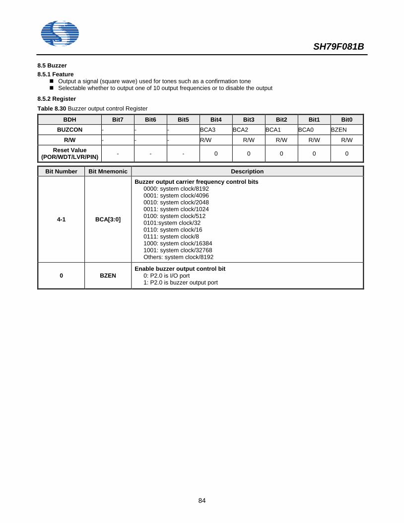
SH79F081B
84
8.5 Buzzer 8.5.1 Feature
Output a signal (square wave) used for tones such as a confirmation tone Selectable whether to output one of 10 output frequencies or to disable the output
8.5.2 Register Table 8.30 Buzzer output control Register
BDH Bit7 Bit6 Bit5 Bit4 Bit3 Bit2 Bit1 Bit0 BUZCON - - - BCA3 BCA2 BCA1 BCA0 BZEN
R/W - - - R/W R/W R/W R/W R/W
Reset Value (POR/WDT/LVR/PIN) - - - 0 0 0 0 0
Bit Number Bit Mnemonic Description
4-1 BCA[3:0]
Buzzer output carrier frequency control bits 0000: system clock/8192 0001: system clock/4096 0010: system clock/2048 0011: system clock/1024 0100: system clock/512 0101:system clock/32 0110: system clock/16 0111: system clock/8 1000: system clock/16384 1001: system clock/32768 Others: system clock/8192
0 BZEN Enable buzzer output control bit
0: P2.0 is I/O port 1: P2.0 is buzzer output port

SH79F081B
85
8.6 Low Voltage Reset (LVR) 8.6.1 Feature
Enabled by the code option and VLVR is 4.1V or 3.7V LVR de-bounce timer TLVR is about 30-60µs An internal reset flag indicates low voltage reset generates
The LVR function is used to monitor the supply voltage and generate an internal reset in the device when the supply voltage below the specified value VLVR. The LVR de-bounce timer TLVR is about 30µs. The LVR circuit has the following functions when the LVR function is enabled: (t means the time of the supply voltage below VLVR) Generates a system reset when VDD ≤ VLVR and t ≥ TLVR; Cancels the system reset when VDD > VLVR or VDD < VLVR, but t < TLVR. The LVR function is enabled by the code option. It is typically used in AC line or large battery supplier applications, where heavy loads may be switched on and cause the MCU supply-voltage temporarily falls below the minimum specified operating voltage. This feature can protect system from working under bad power supply environment.

SH79F081B
86
8.7 Watchdog Timer (WDT) and Reset State 8.7.1 Feature
Auto detect Program Counter (PC) over range, and generate OVL Reset WDT runs even in the Power-Down mode Selectable different WDT overflow frequency
Watchdog Timer The watchdog timer is a down counter, and its clock source is an independent built-in RC oscillator, so it always runs even in the Power-Down mode. The watchdog timer will generate a device reset when it overflows. It can be enabled or disabled permanently by the code option. The watchdog timer control bits (WDT.2-0) are used to select different overflow frequency. The watchdog timer overflow flag (WDOF) will be automatically set to “1” by hardware when overflow happens. To prevent overflow happen, by reading or writing the WDT register RSTSTAT, the watchdog timer should re-count before the overflow happens. OVL Reset To enhance the anti-noise ability, SH79F081B built in Program Counter (PC) over range detect circuit, if program counter value is larger than flash romsize, or detect operation code equal to A5H which is not exist in 8051 instruction set, a OVL reset will be generate to reset CPU, and set WDOF bit. So, to make use of this feature, you should fill unused flash rom with A5H. There are also some reset flags in this register as below:

SH79F081B
87
8.7.2 Register Table 8.31 Reset Control Register
B1H Bit7 Bit6 Bit5 Bit4 Bit3 Bit2 Bit1 Bit0 RSTSTAT WDOF - PORF LVRF CLRF WDT.2 WDT.1 WDT.0
R/W R/W - R/W R/W R/W R/W R/W R/W
Reset Value (POR) 0 - 1 0 0 0 0 0
Reset Value (WDT) 1 - u u u 0 0 0
Reset Value (LVR) u - u 1 u 0 0 0
Reset Value (PIN) u - u u 1 0 0 0
Bit Number Bit Mnemonic Description
7 WDOF
Watch Dog Timer Overflow or OVL Reset Flag Set by hardware when WDT overflow or OVL reset happened, cleared by software or Power On Reset 0: Watch Dog not overflows and no OVL reset generated 1: Watch Dog overflow or OVL reset occurred
5 PORF Power On Reset Flag
Set only by Power On Reset, cleared only by software 0: No Power On Reset. 1: Power On Reset occurred.
4 LVRF Low Voltage Reset Flag
Set only by Low Voltage Reset, cleared by software or Power On Reset 0: No Low Voltage Reset occurs 1: Low Voltage Reset occurred
3 CLRF Pin Reset Flag
Set only by pin reset, cleared by software or Power On Reset 0: No Pin Reset occurs 1: Pin Reset occurred
2-0 WDT[2:0]
WDT Overflow period control bit 000: Overflow period minimal value = 2730.6ms 001: Overflow period minimal value = 682.6ms 010: Overflow period minimal value = 170.6ms 011: Overflow period minimal value = 85.3ms 100: Overflow period minimal value = 42.6ms 101: Overflow period minimal value = 10.6ms 110: Overflow period minimal value = 2.6ms 111: Overflow period minimal value = 0.6ms
Notes: If WDT_opt is enable in application, you must clear Watchdog periodically, and the interval must be less than the value list above.

SH79F081B
88
8.8 Power Management 8.8.1 Feature
Two power saving modes: Idle mode and Power-Down mode Two ways to exit Idle and Power-Down mode: interrupt and reset
To reduce power consumption, SH79F081B supplies two power saving modes: Idle mode and Power-Down mode. These two modes are controlled by PCON & SUSLO register.
8.8.2 Idle Mode In this mode, the clock to CPU is frozen, the program execution is halted, and the CPU will stop at a defined state. But the peripherals continue to be clocked. When entering idle mode, all the CPU status before entering will be preserved. Such as: PSW, PC, SFR & RAM are all retained. By two consecutive instructions: setting SUSLO register as 0x55, and immediately followed by setting the IDL bit in PCON register, will make SH79F081B enter Idle mode. If the consecutive instruction sequence requirement is not met, the CPU will clear either SUSLO register or IDL bit in the next machine cycle. And the CPU will not enter Idle mode. The setting of IDL bit will be the last instruction that CPU executed. There are two ways to exit Idle mode: (1) An interrupt generated. After warm-up time, the clock to the CPU will be restored, and the hardware will clear SUSLO
register and IDL bit in PCON register. Then the program will execute the interrupt service routine first, and then jumps to the instruction immediately following the instruction that activated Idle mode.
(2) Reset signal (logic low on the RESET pin, WDT RESET if enabled, LVR REST if enabled), this will restore the clock to the CPU, the SUSLO register and the IDL bit in PCON register will be cleared by hardware, finally the SH79F081B will be reset. And the program will execute from address 0000H. The RAM will keep unchanged and the SFR value might be changed according to different function module.
8.8.3 Power-Down Mode The Power-Down mode places the SH79F081B in a very low power state. Power-Down mode will stop all the clocks including CPU and peripherals. If WDT is enabled, WDT block will keep on working. When entering Power-Down mode, all the CPU status before entering will be preserved. Such as: PSW, PC, SFR & RAM are all retained. By two consecutive instructions: setting SUSLO register as 0x55, and immediately followed by setting the PD bit in PCON register, will make SH79F081B enter Power-Down mode. If the consecutive instruction sequence requirement is not met, the CPU will clear either SUSLO register or PD bit in the next machine cycle. And the CPU will not enter Power-Down mode. The setting of PD bit will be the last instruction that CPU executed. Note: If IDL bit and PD bit are set simultaneously, the SH79F081B enters Power-Down mode. The CPU will not go in Idle mode when exiting from Power-Down mode, and the hardware will clear both IDL & PD bit after exit form Power-Down mode. There are two ways to exit the Power-Down mode: (1) An active external Interrupt such as INT0, INT1 & INT4 will make SH79F081B exit Power-Down mode. The oscillator will
start after interrupt happens, after warm-up time, the clocks to the CPU and peripheral will be restored, the SUSLO register and PD bit in PCON register will be cleared by hardware. Program execution resumes with the interrupt service routine. After completion of the interrupt service routine, program execution resumes with the instruction immediately following the instruction that activated Power-Down mode.
(2) Reset signal (logic low on the RESET pin, WDT RESET if enabled, LVR REST if enabled). This will restore the clock to the CPU after warm-up time, the SUSLO register and the PD bit in PCON register will be cleared by hardware, finally the SH79F081B will be reset. And the program will execute from address 0000H. The RAM will keep unchanged and the SFR value might be changed according to different function module.
Note: In order to entering Idle/Power-Down, it is necessary to add 3 NOPs after setting IDL/PD bit in PCON.

SH79F081B
89
8.8.4 Register Table 8.32 Power Control Register
87H Bit7 Bit6 Bit5 Bit4 Bit3 Bit2 Bit1 Bit0 PCON SMOD SSTAT - - GF1 GF0 PD IDL
R/W R/W R/W - - R/W R/W R/W R/W
Reset Value (POR/WDT/LVR/PIN) 0 0 - - 0 0 0 0
Bit Number Bit Mnemonic Description 7 SMOD Baud rate double bit 6 SSTAT SCON[7:5] function selection bit
3-2 GF[1:0] General purpose flags for software use
1 PD Power-Down mode control bit
0: Cleared by hardware when an interrupt or reset occurs 1: Set by software to activate the Power-Down mode
0 IDL Idle mode control bit
0: Cleared by hardware when an interrupt or reset occurs 1: Set by software to activate the Idle mode
Table 8.33 Suspend Mode Control Register
8EH Bit7 Bit6 Bit5 Bit4 Bit3 Bit2 Bit1 Bit0 SUSLO SUSLO.7 SUSLO.6 SUSLO.5 SUSLO.4 SUSLO.3 SUSLO.2 SUSLO.1 SUSLO.0
R/W R/W R/W R/W R/W R/W R/W R/W R/W
Reset Value (POR/WDT/LVR/PIN) 0 0 0 0 0 0 0 0
Bit Number Bit Mnemonic Description
7-0 SUSLO[7:0] This register is used to control the CPU enter suspend mode (Idle or Power-Down). Only consecutive instructions like below will make CPU enter suspend mode. Other wise the either SUSLO, IDL or PD bit will be cleared by hardware in the next machine cycle.
Example:
IDLE_MODE: MOV SUSLO, #55H ORL PCON, #01H NOP NOP NOP
POWERDOWN_MODE: MOV SUSLO, #55H ORL PCON, #02H NOP NOP NOP

SH79F081B
90
8.9 Warm-up Timer 8.9.1 Feature
Built-in power on warm-up counter to eliminate unstable state of power on Built-in oscillator warm-up counter to eliminate unstable state when oscillation startup
SH79F081B has a built-in power warm-up counter; it is designed to eliminate unstable state after power on or to do some internal initial operation such as read customer option etc. SH79F081B has also a built-in oscillator warm-up counter, it is designed to eliminate unstable state when oscillator starts oscillating in the following conditions: Power-on reset, Pin reset, LVR reset, Watchdog Reset and Wake up from Power-down mode. After power-on, SH79F081B will start power warm-up procedure first, and then oscillator warm-up procedure. Power Warm-up Time
Power On Reset/ Pin Reset/
Low Voltage Reset WDT Reset
(Not in Power-Down Mode) WDT Reset
(Wakeup from Power-Down Mode)
Wakeup from Power-Down Mode
(Only for interrupt)
TPWRT** OSC Warm up* TPWRT** OSC
Warm up* TPWRT** OSC Warm up* TPWRT** OSC
Warm up*
11ms YES 1000CKs NO 1000 CKs YES 64CKs YES
Note: * This count clock is a 2MHz internal RC. ** Oscillator warm-up time, please refer to the table below.
OSC Warm-up Time
Option: OP_WMT
Oscillator Type 00 01 10 11
Ceramic/Crystal 217 X Tosc 214 X Tosc 211 X Tosc 28 X Tosc
Internal RC 27 X Tosc

SH79F081B
91
8.10 Code Option OP_OSC:
0000: Internal 12.3MHz RC oscillator (Default) 0001: Internal 16MHz RC oscillator 1110: Crystal oscillator or Ceramic resonator Others: Internal 12.3MHz RC oscillator
OP_CRMC: 0: Oscillator frequency is 4M-16M (Default) 1: Oscillator frequency is 400K-2M
OP_HPEN: 0: Oscillator frequency is 4M-12M (Default) 1: Oscillator frequency is 16M Note: This Option is valid only when OP_CRMC = 0
OP_RST: 0: P1.7 used as RST pin (Default) 1: P1.7 used as I/O pin
OP_LVREN: 0: Disable LVR function (Default) 1: Enable LVR function
OP_LVRLE: 0: 4.1V LVR level 1 (Default) 1: 3.7V LVR level 2
OP_WDT: 0: Disable WDT function (Default) 1: Enable WDT function
OP_WDTPD: 0: Disable WDT function in Power-Down mode (Default) 1: Enable WDT function in Power-Down mode Note: This Option is valid only when OP_WDT = 1
OP_WMT: (Unavailable for Internal RC) 00: longest warm up time (Default) 01: longer warm up time 10: shorter warm up time 11: shortest warm up time
OP_OVL: 0: Generated OVL reset 1: Generated OVL interrupt (Default)
OP_SCM: 0: SCM is valid in warm up period (Default) 1: SCM is invalid in warm up period

SH79F081B
92
9. Instruction Set
ARITHMETIC OPERATIONS
Opcode Description Code Byte Cycle ADD A, Rn Add register to accumulator 0x28-0x2F 1 1 ADD A, direct Add direct byte to accumulator 0x25 2 2 ADD A, @Ri Add indirect RAM to accumulator 0x26-0x27 1 2 ADD A, #data Add immediate data to accumulator 0x24 2 2 ADDC A, Rn Add register to accumulator with carry flag 0x38-0x3F 1 1
ADDC A, direct Add direct byte to A with carry flag 0x35 2 2 ADDC A, @Ri Add indirect RAM to A with carry flag 0x36-0x37 1 2 ADDC A, #data Add immediate data to A with carry flag 0x34 2 2 SUBB A, Rn Subtract register from A with borrow 0x98-0x9F 1 1 SUBB A, direct Subtract direct byte from A with borrow 0x95 2 2 SUBB A, @Ri Subtract indirect RAM from A with borrow 0x96-0x97 1 2 SUBB A, #data Subtract immediate data from A with borrow 0x94 2 2 INC A Increment accumulator 0x04 1 1 INC Rn Increment register 0x08-0x0F 1 2 INC direct Increment direct byte 0x05 2 3 INC @Ri Increment indirect RAM 0x06-0x07 1 3 DEC A Decrement accumulator 0x14 1 1 DEC Rn Decrement register 0x18-0x1F 1 2 DEC direct Decrement direct byte 0x15 2 3 DEC @Ri Decrement indirect RAM 0x16-0x17 1 3 INC DPTR Increment data pointer 0xA3 1 4 MUL AB 8 X 8
16 X 8 Multiply A and B 0xA4 1 11 20
DIV AB 8 / 8 16 / 8 Divide A by B 0x84 1 11
20 DA A Decimal adjust accumulator 0xD4 1 1

SH79F081B
93
LOGIC OPERATIONS
Opcode Description Code Byte Cycle ANL A, Rn AND register to accumulator 0x58-0x5F 1 1 ANL A, direct AND direct byte to accumulator 0x55 2 2 ANL A, @Ri AND indirect RAM to accumulator 0x56-0x57 1 2 ANL A, #data AND immediate data to accumulator 0x54 2 2 ANL direct, A AND accumulator to direct byte 0x52 2 3 ANL direct, #data AND immediate data to direct byte 0x53 3 3 ORL A, Rn OR register to accumulator 0x48-0x4F 1 1 ORL A, direct OR direct byte to accumulator 0x45 2 2 ORL A, @Ri OR indirect RAM to accumulator 0x46-0x47 1 2 ORL A, #data OR immediate data to accumulator 0x44 2 2 ORL direct, A OR accumulator to direct byte 0x42 2 3 ORL direct, #data OR immediate data to direct byte 0x43 3 3 XRL A, Rn Exclusive OR register to accumulator 0x68-0x6F 1 1 XRL A, direct Exclusive OR direct byte to accumulator 0x65 2 2 XRL A, @Ri Exclusive OR indirect RAM to accumulator 0x66-0x67 1 2 XRL A, #data Exclusive OR immediate data to accumulator 0x64 2 2 XRL direct, A Exclusive OR accumulator to direct byte 0x62 2 3 XRL direct, #data Exclusive OR immediate data to direct byte 0x63 3 3 CLR A Clear accumulator 0xE4 1 1 CPL A Complement accumulator 0xF4 1 1 RL A Rotate accumulator left 0x23 1 1 RLC A Rotate accumulator left through carry 0x33 1 1 RR A Rotate accumulator right 0x03 1 1 RRC A Rotate accumulator right through carry 0x13 1 1 SWAP A Swap nibbles within the accumulator 0xC4 1 4

SH79F081B
94
DATA TRANSFERS
Opcode Description Code Byte Cycle MOV A, Rn Move register to accumulator 0xE8-0xEF 1 1 MOV A, direct Move direct byte to accumulator 0xE5 2 2 MOV A, @Ri Move indirect RAM to accumulator 0xE6-0xE7 1 2 MOV A, #data Move immediate data to accumulator 0x74 2 2 MOV Rn, A Move accumulator to register 0xF8-0xFF 1 2 MOV Rn, direct Move direct byte to register 0xA8-0xAF 2 3 MOV Rn, #data Move immediate data to register 0x78-0x7F 2 2 MOV direct, A Move accumulator to direct byte 0xF5 2 2 MOV direct, Rn Move register to direct byte 0x88-0x8F 2 2 MOV direct1, direct2 Move direct byte to direct byte 0x85 3 3 MOV direct, @Ri Move indirect RAM to direct byte 0x86-0x87 2 3 MOV direct, #data Move immediate data to direct byte 0x75 3 3 MOV @Ri, A Move accumulator to indirect RAM 0xF6-0xF7 1 2 MOV @Ri, direct Move direct byte to indirect RAM 0xA6-0xA7 2 3 MOV @Ri, #data Move immediate data to indirect RAM 0x76-0x77 2 2 MOV DPTR, #data16 Load data pointer with a 16-bit constant 0x90 3 3 MOVC A, @A+DPTR Move code byte relative to DPTR to A 0x93 1 7 MOVC A, @A+PC Move code byte relative to PC to A 0x83 1 8 MOVX A, @Ri Move external RAM (8-bit address) to A 0xE2-0xE3 1 5 MOVX A, @DPTR Move external RAM (16-bit address) to A 0xE0 1 6 MOVX @Ri, A Move A to external RAM (8-bit address) 0xF2-F3 1 4 MOVX @DPTR, A Move A to external RAM (16-bit address) 0xF0 1 5 PUSH direct Push direct byte onto stack 0xC0 2 5 POP direct Pop direct byte from stack 0xD0 2 4 XCH A, Rn Exchange register with accumulator 0xC8-0xCF 1 3 XCH A, direct Exchange direct byte with accumulator 0xC5 2 4 XCH A, @Ri Exchange indirect RAM with accumulator 0xC6-0xC7 1 4 XCHD A, @Ri Exchange low-order nibble indirect RAM with A 0xD6-0xD7 1 4

SH79F081B
95
PROGRAM BRANCHES
Opcode Description Code Byte Cycle ACALL addr11 Absolute subroutine call 0x11-0xF1 2 7 LCALL addr16 Long subroutine call 0x12 3 7 RET Return from subroutine 0x22 1 8 RETI Return from interrupt 0x32 1 8 AJMP addr11 Absolute jump 0x01-0xE1 2 4 LJMP addr16 Long jump 0x02 3 5 SJMP rel Short jump (relative address) 0x80 2 4 JMP @A+DPTR Jump indirect relative to the DPTR 0x73 1 6 JZ rel (not taken)
(taken) Jump if accumulator is zero 0x60 2 3 5
JNZ rel (not taken) (taken) Jump if accumulator is not zero 0x70 2 3
5 JC rel (not taken)
(taken) Jump if carry flag is set 0x40 2 2 4
JNC rel (not taken) (taken) Jump if carry flag is not set 0x50 2 2
4 JB bit, rel (not taken)
(taken) Jump if direct bit is set 0x20 3 4 6
JNB bit, rel (not taken) (taken) Jump if direct bit is not set 0x30 3 4
6 JBC bit, rel (not taken)
(taken) Jump if direct bit is set and clear bit 0x10 3 4 6
CJNE A, direct, rel (not taken) (taken) Compare direct byte to A and jump if not equal 0xB5 3 4
6 CJNE A, #data, rel (not taken)
(taken) Compare immediate to A and jump if not equal 0xB4 3 4 6
CJNE Rn, #data, rel (not taken) (taken) Compare immediate to reg. and jump if not equal 0xB8-0xBF 3 4
6 CJNE @Ri, #data, rel (not taken)
(taken) Compare immediate to Ri and jump if not equal 0xB6-0xB7 3 4 6
DJNZ Rn, rel (not taken) (taken) Decrement register and jump if not zero 0xD8-0xDF 2 3
5 DJNZ direct, rel (not taken)
(taken) Decrement direct byte and jump if not zero 0xD5 3 4 6
NOP No operation 0 1 1

SH79F081B
96
BOOLEAN MANIPULATION
Opcode Description Code Byte Cycle CLR C Clear carry flag 0xC3 1 1 CLR bit Clear direct bit 0xC2 2 3 SETB C Set carry flag 0xD3 1 1 SETB bit Set direct bit 0xD2 2 3 CPL C Complement carry flag 0xB3 1 1 CPL bit Complement direct bit 0xB2 2 3 ANL C, bit AND direct bit to carry flag 0x82 2 2 ANL C, /bit AND complement of direct bit to carry 0xB0 2 2 ORL C, bit OR direct bit to carry flag 0x72 2 2 ORL C, /bit OR complement of direct bit to carry 0xA0 2 2 MOV C, bit Move direct bit to carry flag 0xA2 2 2 MOV bit, C Move carry flag to direct bit 0x92 2 3

SH79F081B
97
10. Electrical Characteristics
Absolute Maximum Ratings* DC Supply Voltage . . . . . . . . . . . . . . . . . . . -0.3V to +6.0V
Input/Output Voltage. . . . . . . . . . . GND-0.3V to VDD+0.3V
Operating Ambient Temperature. . . . . . . . .-40°C to +85°C
Storage Temperature. . . . . . . . . . .. . . . . .-55°C to +125°C
*Comments Stresses exceed those listed under “Absolute Maximum Ratings” may cause permanent damage to this device. These are stress ratings only. Functional operation of this device at these or any other conditions above those indicated in the operational sections of this specification is not implied or intended. Exposure to the absolute maximum rating conditions for extended periods may affect device reliability.
DC Electrical Characteristics (VDD =3.6 - 5.5V, GND = 0V, TA = 25°C, unless otherwise specified)
Parameter Symbol Min. Typ. ∗ Max. Unit Condition Operating Voltage VDD 3.6 5.0 5.5 V 400kHz ≤ fOSC ≤ 16MHz
Operating Current
IOP1 - 5 8 mA
fOSC = 12MHz, VDD = 5.0V All output pins unload (including all digital input pins unfloating) CPU on (execute NOP instruction), WDT on, all other function block off
IOP2 - 8 12 mA
fOSC = 16MHz, VDD = 5.0V All output pins unload (including all digital input pins unfloating) CPU on (execute NOP instruction), WDT on, all other function block off
Stand by Current (IDLE)
ISB1 - 3 5 mA
fOSC = 12MHz, VDD = 5.0V All output pins unload (including all digital input pins unfloating) CPU on (execute NOP instruction), WDT on, all other function block off
ISB2 - 6 10 mA
fOSC = 16MHz, VDD = 5.0V All output pins unload (including all digital input pins unfloating) CPU on (execute NOP instruction), WDT on, all other function block off
Stand by Current (Power-Down) ISB3 - - 15 µA
Osc off, VDD = 5.0V All output pins unload(including all digital input pins unfloating), CPU off (Power-Down), LVR off, LCD off, WDT off, all other function block off
WDT Current IWDT - 1 3 µA All output pins unload, WDT on, VDD = 5.0V Input Low Voltage 1 VIL1 GND - 0.3 X VDD V I/O Ports Input High Voltage 1 VIH1 0.7 X VDD - VDD V I/O Ports
Input Low Voltage 2 VIL2 GND - 0.2 X VDD V RESET——-------——
, T0, T1, T2, INT0/1/2/3/4, SCK, T2EX, RXD (RXDCON[0] = 0), SS
———FLT MISO, MOSI
Input High Voltage 2 VIH2 0.8 X VDD - VDD V RESET——-------——
, T0, T1, T2, INT0/1/2/3/4, SCK, T2EX, RXD (RXDCON[0] = 0), SS
———FLT MISO, MOSI
Input Low Voltage 3 VIL3 GND - 0.2 X VDD V RXD (RXDCON[0] = 1), VDD = 3.6 - 5.5V Input High Voltage 3 VIH3 0.55 X VDD - VDD V RXD (RXDCON[0] = 1), VDD = 3.6 - 5.5V Input Leakage Current IIL -1 - 1 µA Input pad, VIN = VDD or GND Output Leakage Current IOL -1 - 1 µA Open-drain, Vout = VDD or GND Pull-high Resistor RPH - 20 - kΩ VDD = 5.0V, VIN = GND Output High Voltage VOH VDD - 0.7 - - V I/O Ports, IOH = -10mA, VDD = 5.0V Output Low Voltage VOL1 - - GND + 0.6 V I/O Ports, IOL = 15mA, VDD = 5.0V
Note: (1) “∗” Data in “Typ.” Column is at 5.0V, 25°C, unless otherwise specified. (2) Maximum value of the supply current to VDD is 150mA. (3) Maximum value of the output current from GND is 200mA.

SH79F081B
98
A/D Converter Electrical Characteristics (VDD = 3.6 - 5.5V, GND = 0V, TA = -25°C, unless otherwise specified)
Parameter Symbol Min. Typ. Max. Unit Condition Supply Voltage VAD 3.6 5.0 5.5 V Resolution NR - 10 - bit GND ≤ VAIN ≤ VREF A/D Input Voltage VAIN GND - VREF V A/D Input Resistor* RAIN 2 - - MΩ VIN = 5.0V Recommended impedance of analog voltage source
ZAIN - - 10 kΩ
A/D conversion current IAD - 1 3 mA ADC module operating, VDD = 5.0V A/D Input current IADIN - - 10 µA VDD = 5.0V Differential linearity error DLE - - ±1 LSB VDD = 5.0V Integral linearity error ILE - - ±2 LSB VDD = 5.0V Full scale error EF - ±1 ±3 LSB VDD = 5.0V Offset error EZ - ±0.5 ±2 LSB VDD = 5.0V Total Absolute error EAD - - ±3 LSB VDD = 5.0V Total Conversion time** TCON 14 - - tAD 10 bit Resolution, VDD = 5.0V
Note: (1) “∗” Here the A/D input Resistor is the DC input-resistance of A/D itself. (2) "**" Recommendations ADC connected signal source resistance of less than10kΩ
AC Electrical Characteristics (VDD = 3.6V - 5.5V, GND = 0V, TA = 25°C, fOSC = 16.6MHz, unless otherwise specified)
Parameter Symbol Min. Typ. Max. Unit Condition RESET pulse width tRESET 10 - - µs Low active
RESET Pull-high Resistor RRPH - 100 - kΩ VDD = 5.0V, VIN = GND
RC1 Frequency FRC1 - 12.3 - MHz VDD = 5V
RC2 Frequency FRC2 - 16 - MHz VDD = 5V
Frequency Stability (RC 12.3MHz) | ∆ F1|/F1
- - 0.5 % RC Oscillator 1: |F-12.3MHz|/12.3MHz (VDD = 3.6-5.5V, TA = +25°C)
- - 2 % RC Oscillator 1: |F-12.3MHz|/12.3MHz (VDD= 3.6-5.5V, TA = -40°C~85°C)
Frequency Stability (RC 16MHz) | ∆ F2|/F2
- - 0.5 % RC Oscillator 2: |F-16MHz|/16MHz (VDD = 3.6-5.5V, TA = +25°C)
- - 2 % RC Oscillator 2: |F-16MHz|/16MHz (VDD= 3.6-5.5V, TA = -40°C~85°C)
Low Voltage Reset Electrical Characteristics (VDD = 3.3V - 5.5V, GND = 0V, TA = +25°C, unless otherwise specified)
Parameter Symbol Min. Typ. Max. Unit Condition LVR Voltage1 VLVR 4.0 4.1 4.2 V LVR1 enabled (VDD = 3.6V - 5.5V) LVR Voltage2 VLVR 3.6 3.7 3.8 V LVR2 enabled (VDD = 3.6V - 5.5V)
Drop-Down Pulse Width for LVR TLVR - 30 - µs

SH79F081B
99
11. Ordering Information
Part No. Package
SH79F081BM/028MU 28 SOP

SH79F081B
100
12. Package Information SOP28L Outline Dimensions unit: inch/mm
1
E HE
L
c
14
See Detail F
Detail Fb
1528
A1
A2
A
D
Seating Plane
e
θ2
Symbol Dimensions in inches Dimensions in mm
Min Max Min Max A 0.085 0.104 2.15 2.65 A1 0.004 0.012 0.10 0.30 A2 0.081 0.098 2.05 2.50 b 0.013 0.02 0.33 0.51 c 0.006 0.014 0.15 0.36 D 0.697 0.715 17.70 18.15 E 0.291 0.303 7.40 7.70 e 0.050 (BSC) 1.27 (BSC)
HE 0.398 0.418 10.10 10.61 L 0.016 0.05 0.40 1.27
θ2 0° 8° 0° 8°
Notice: (1) Both package length and width do not include mold flash. (2) Tolerance is ±0.1mm if not specified. (3) Coplanarity: 0.1mm max. (4) Controlling dimension: mm.

SH79F081B
101
13. Product SPEC. Change Notice
Version Content Date
2.0 Update Package Information, Change Code Option OP_CRMC, OP_HPEN. Mar. 2019
1.0 Original Nov. 2016

SH79F081B
102
Content 1. FEATURES ..................................................................................................................................................................... 1 2. GENERAL DESCRIPTION .............................................................................................................................................. 1 3. BLOCK DIAGRAM .......................................................................................................................................................... 2 4. PIN CONFIGURATION ................................................................................................................................................... 3 28 SOP ........................................................................................................................................................................................................ 3
5. PIN DESCRIPTION ......................................................................................................................................................... 5 6. SFR MAPPING ................................................................................................................................................................ 7 7. NORMAL FUNCTION ................................................................................................................................................... 14 7.1 CPU .................................................................................................................................................................................................... 14
7.1.1 CPU Core SFR ............................................................................................................................................................................ 14 7.1.2 Enhanced CPU core SFRs ........................................................................................................................................................... 15
7.2 RAM ................................................................................................................................................................................................... 16 7.3 FLASH PROGRAM MEMORY .................................................................................................................................................................. 17
7.3.1 Features ....................................................................................................................................................................................... 17 7.3.2 Flash Operation in ICP Mode ..................................................................................................................................................... 19
7.4 SSP FUNCTION ..................................................................................................................................................................................... 20 7.4.1 SSP Register ................................................................................................................................................................................ 20 7.4.2 Flash Control Flow...................................................................................................................................................................... 23 7.4.3 SSP Programming Notice ............................................................................................................................................................ 24 7.4.4 Readable Random Code............................................................................................................................................................... 24
7.5 SYSTEM CLOCK AND OSCILLATOR ........................................................................................................................................................ 25 7.5.1 Feature ........................................................................................................................................................................................ 25 7.5.2 Clock Definition ........................................................................................................................................................................... 25 7.5.3 Oscillator Type ............................................................................................................................................................................ 26 7.5.4 Capacitor Selection for Oscillator ............................................................................................................................................... 26
7.6 SYSTEM CLOCK MONITOR (SCM) ........................................................................................................................................................ 27 7.7 I/O PORT .............................................................................................................................................................................................. 28
7.7.1 Feature ........................................................................................................................................................................................ 28 7.7.2 Register ........................................................................................................................................................................................ 28 7.7.3 Port Diagram ............................................................................................................................................................................... 30 7.7.4 Port Share .................................................................................................................................................................................... 31
7.8 TIMER .................................................................................................................................................................................................. 35 7.8.1 Feature ........................................................................................................................................................................................ 35 7.8.2 Timer0/1 ...................................................................................................................................................................................... 35 7.8.3 Timer2 ......................................................................................................................................................................................... 39
7.9 INTERRUPT ........................................................................................................................................................................................... 45 7.9.1 Feature ........................................................................................................................................................................................ 45 7.9.2 Program Over Range Interrupt (OVL) ........................................................................................................................................ 45 7.9.3 Interrupt Enable Control ............................................................................................................................................................. 46 7.9.4 Interrupt Flag .............................................................................................................................................................................. 48 7.9.5 Interrupt Vector ........................................................................................................................................................................... 50 7.9.6 Interrupt Priority ......................................................................................................................................................................... 50 7.9.7 Interrupt Handling ....................................................................................................................................................................... 51 7.9.8 Interrupt Response Time .............................................................................................................................................................. 51 7.9.9 External Interrupt Inputs ............................................................................................................................................................. 52 7.9.10 Interrupt Summary ..................................................................................................................................................................... 52
8. ENHANCED FUNCTION ............................................................................................................................................... 53 8.1 PWM (PULSE WIDTH MODULATION) ................................................................................................................................................... 53
8.1.1 Feature ........................................................................................................................................................................................ 53 8.1.2 12-bit PWM Timer ....................................................................................................................................................................... 54 8.1.3 8-bit PWM Timer ......................................................................................................................................................................... 57 8.1.4 PWM01/11/21 .............................................................................................................................................................................. 60 8.1.5 Dead Time ................................................................................................................................................................................... 60
8.2 SERIAL PERIPHERAL INTERFACE (SPI) .................................................................................................................................................. 62 8.2.1 Features ....................................................................................................................................................................................... 62 8.2.2 Signal Description ....................................................................................................................................................................... 62 8.2.3 Baud Rate .................................................................................................................................................................................... 63 8.2.4 Functional Description ................................................................................................................................................................ 63 8.2.5 Operating Modes ......................................................................................................................................................................... 64 8.2.6 Transmission Formats ................................................................................................................................................................. 66 8.2.7 Error Conditions .......................................................................................................................................................................... 67

SH79F081B
103
8.2.8 Interrupts ..................................................................................................................................................................................... 67 8.2.9 Registers ...................................................................................................................................................................................... 68
8.3 EUART ............................................................................................................................................................................................... 70 8.3.1 Feature ........................................................................................................................................................................................ 70 8.3.2 EUART Mode Description ........................................................................................................................................................... 70 8.3.3 Baud Rate Generate ..................................................................................................................................................................... 75 8.3.4 Multi-Processor Communication ................................................................................................................................................. 75 8.3.5 Error Detection ............................................................................................................................................................................ 76 8.3.6 Register ........................................................................................................................................................................................ 77
8.4 ANALOG DIGITAL CONVERTER (ADC) ................................................................................................................................................. 80 8.4.1 Feature ........................................................................................................................................................................................ 80 8.4.2 ADC Diagram .............................................................................................................................................................................. 80 8.4.3 ADC Register ............................................................................................................................................................................... 81
8.5 BUZZER ............................................................................................................................................................................................... 84 8.5.1 Feature ........................................................................................................................................................................................ 84 8.5.2 Register ........................................................................................................................................................................................ 84
8.6 LOW VOLTAGE RESET (LVR) ............................................................................................................................................................... 85 8.6.1 Feature ........................................................................................................................................................................................ 85
8.7 WATCHDOG TIMER (WDT) AND RESET STATE ..................................................................................................................................... 86 8.7.1 Feature ........................................................................................................................................................................................ 86 8.7.2 Register ........................................................................................................................................................................................ 87
8.8 POWER MANAGEMENT ......................................................................................................................................................................... 88 8.8.1 Feature ........................................................................................................................................................................................ 88 8.8.2 Idle Mode ..................................................................................................................................................................................... 88 8.8.3 Power-Down Mode ...................................................................................................................................................................... 88 8.8.4 Register ........................................................................................................................................................................................ 89
8.9 WARM-UP TIMER ................................................................................................................................................................................. 90 8.9.1 Feature ........................................................................................................................................................................................ 90
8.10 CODE OPTION .................................................................................................................................................................................... 91 9. INSTRUCTION SET ...................................................................................................................................................... 92 10. ELECTRICAL CHARACTERISTICS ............................................................................................................................. 97 11. ORDERING INFORMATION ......................................................................................................................................... 99 12. PACKAGE INFORMATION ......................................................................................................................................... 100 13. PRODUCT SPEC. CHANGE NOTICE ........................................................................................................................ 101