low standby power 8051 mcu with 64k/32k/16k flash and 2k ...ams.issi.com/ww/pdf/is32cs8964.pdf ·...
TRANSCRIPT

IS32CS8964
Low Standby Power 8051 MCU with 64K/32K/16K Flash and 2K/1K SRAM
CONFIDENTIAL INFORMATION
Revision 0A 2019-3-5
Integrated Silicon Solution, Inc. (ISSI) ams.issi.com
GENERAL DESCRIPTION
IS32CS8964 is a general-purpose microcontroller with extensive peripherals suitable for a wide range of applications. The CPU utilizes an enhanced 1-cycle 8051 core equivalent to ten times the speed of a conventional 12-T 8051. The total on-chip memory includes a 2KB SRAM and 64KB embedded flash memory that can be used as program memory which may also serve as the flash memory. The 8051 core has built-in T0/T1/T2/T3/T4/T5 timers and a 30-bit watchdog timer. Embedded in the CPU core are also a full-duplex UART ports, one I
2C master/slave and one
I2C pure slave controllers, up to 28 GPIO pins with each
GPIO pin configurable as external interrupt and wake up.
The flexibility in clock setting includes an on-chip precision oscillator with the accuracy deviation of +/-5%, or a slow power internal 100K Hz oscillator, and an external 4MHz to 24MHz crystal oscillator, or an ultra low power precision real time clock (RTC). Unused clock sources can be disabled or used as GPIO pins for system optimization. The clock selections are combined with flexible power management schemes, including PMM, IDLE, and STOP, SLEEP modes to balance CPU speed and power consumption.
On-chip peripherals include one SPI control interface, one I
2C master/slave and one I
2C pure slave
controllers. A Programmable Counter Array (PCA) with 6 channels of Capture/Compare/PWM modules can be used for varieties purposes controlling external devices. There is an additional 3 channel complementary 16-Bit center-aligned PWM for driving various kinds of motor.
Analog peripherals include a high performance 12-Bit Analog to Digital Converter (ADC) with 3.5usec conversion time, 4 analog comparators with programmable threshold levels, and a 10-bit Voltage Output Digital to Analog Converter (VDAC).
IS32CS8964 also provides a flexible means of flash programming that supports ISP and IAP. The protection of data loss is implemented in hardware. Access restriction on critical registers and low supply voltage detection allow reliable operations under harsh environments. The code security is reinforced with sophisticated writer commands and ISP commands. The on-chip break point processor also allows easy debugging which can be integrated with ISP.
Intended applications of IS32CS8964 include battery operated systems, home appliances, industrial control, motor control and other embedded applications.
FEATURES
CPU and Memory
1-Cycle 8051 CPU core up to 24MHz (16MHz Zero Wait State)
16-bit Timers T0/T1/T2/T3/T4 and 24-bit T5
Programmable 30-bit Watch Dog Timer
Integrated break point controller and debug port through I
2C slave
FEATURES Cont. One full-duplex UART0 port
Up to 8 external interrupts shared with GPIO pins
Power saving modes – PMM, IDLE, STOP, and SLEEP modes
256B Internal SRAM and 1792B XSRAM
64KB Flash Memory and 128B Information Block Configured to be shared by ISP code, program code,
and data flash
Code security and data loss protection
Endurance: 100K cycles
Retention: 10 years
Clock Sources
Adjustable Internal oscillator from 8MHz to 16MHz at +/- 2% accuracy@-40°C to 85°C; +/- 5% accuracy@-40°C to 105°C
Internal low power OSC of 100KHz
Crystal oscillator 4MHz – 24MHz
RTC - 32KHz of low power consumption
Digital Peripherals
16-bit PCA and 6 channel of CCP modules Capture/Compare/Timer Mode
8-Bit and 16-bit PWM Mode
8-Bit Windowed PWM Mode
16-bit PWM Controller 3 channels of center PWM with complementary outputs
2 channels ADC and interrupt triggering
Dead time setting
Emergency control
Two I2C Slave Controllers
One Master/Slave SPI Controller
One full-duplex LIN-capable EUART2
Analog Peripherals
12-Bit monotonic SAR ADC 1 channels with a built-in 7X PGA
4usec conversion time
2 S/H channels triggered by PWM16 or software
15 inputs multiplexed with GPIO
On-chip temperature sensor
4 analog comparators Two 8-bit programmable threshold or external threshold
Linked to PWM16 module for emergency
10-bit Voltage Output DAC Source resistance < 1KOhm
0 – VDD output range
Power on reset
Low voltage detection on supply voltage
Miscellaneous
Up to 28 GPIO pins
2.5V to 5.5V single supply with on-chip regulator
Low power standby (< 10uA) in SLEEP mode
Operating temperature -40℃ to 105℃
AEC-Q100 qualification (Pending)
QFN-32 package and RoHS compliant

IS32CS8964
Revision 0A 2019-3-5
This Data sheet contains confidential and proprietary information of ISSI. Recipient shall not disclose this confidential information to any other
person or entity, nor should use for the purpose of infringement or competition with ISSI.
Page 2 of 122
BLOCK DIAGRAM
1-CYCLE
8051
FL
AS
H
CO
NT
RO
L
64KB
FLASH
2KB
IRAM/XRAM
SIOSC
4 ANALOG
COMPARATOR
I/O
MU
LT
IPL
EX
ER
AN
D B
UF
FE
RS
I2CS1
SLAVE
I2CM0
MASTER
IOSC
I/O MULTIPLEXER AND BUFFERS
XOSCREGULATOR
UART0
EUART2
TIMER[0-5]
6 CH
CCP/PWM
PCA12-BIT SAR ADC
4 CH INPUT
PORT0
PORT1
PORT2
PORT3
128B
IFB
LOW
SUPPLY
DETECT
RESET
2-CH S/H
RTC
I2CS2
ISP/DBG
10-BIT
DAC
2CH TRG
3 CH of PWM
PWM16
REF
7X PGA

IS32CS8964
Revision 0A 2019-3-5
This Data sheet contains confidential and proprietary information of ISSI. Recipient shall not disclose this confidential information to any other
person or entity, nor should use for the purpose of infringement or competition with ISSI.
Page 3 of 122
PIN CONNECTION
Note: The part number of description in this section is only for pin assignment and not the actual marking or logo.
P1
.6/T
1/C
EX
0/P
WM
BP
/AD
D9
P1
.3/S
SC
L1
/CE
X3
/PW
MA
N/A
DD
8
P1
.2/S
SD
A1
/CE
X2
/PW
MA
P/A
DD
7
P3
.1/P
WM
CP
/CE
X3
/AD
D6
P3
.0/P
WM
CN
/CE
X2
/AD
D5
P1
.5/S
SD
A2
/MS
DA
/PW
MB
N/R
XIN
P1
.4/S
SC
L2
/MS
CL
/PW
MB
P/R
XO
UT
1
P1.1/PWMAN/CEX1/ADD4
P1.0/PWMAP/CEX0/ADD3
P0.7/RXD0/RXD2/ADD2
P0.6/TXD0/TXD2/ADC2
P0.5/XEMG/ADA3
P0.4/ADB3
P0.3/ADB1
P0.2/ADA1
VSS
P2.0/CEX4/MOSI/MSCL/SSCL1/XIN
P2.1/CEX5/MISO/MSDA/SSDA1/XOUT
P2.2/TXD2/SCK/XEMG/VDAC
P2.3/RXD2/SSN/XEMG/CMPTH
P2.4/T2/PWMCP/CMPD
P2.5/CEX4/PWMCN/CMPC
P2.6/CEX5/SSN/CMPB
P2
.7/X
EM
G/T
2E
X/S
CK
/CM
PA
P3
.2/C
EX
4/T
XD
2/M
OS
I/V
DA
C
P3
.3/C
EX
5/R
XD
2/M
ISO
/CM
PA
RS
TN
VD
D
VD
DC
P0
.0/C
EX
4/S
SN
/AD
A2
P0
.1/C
EX
5/A
DB
2
IS32CS8964QFN-32
1
P1
.7/T
0/C
EX
1/P
WM
BN
/VD
AC
IS32CS8964
Revision 0A 2019-3-5
This Data sheet contains confidential and proprietary information of ISSI. Recipient shall not disclose this confidential information to any other
person or entity, nor should use for the purpose of infringement or competition with ISSI.
Page 4 of 122
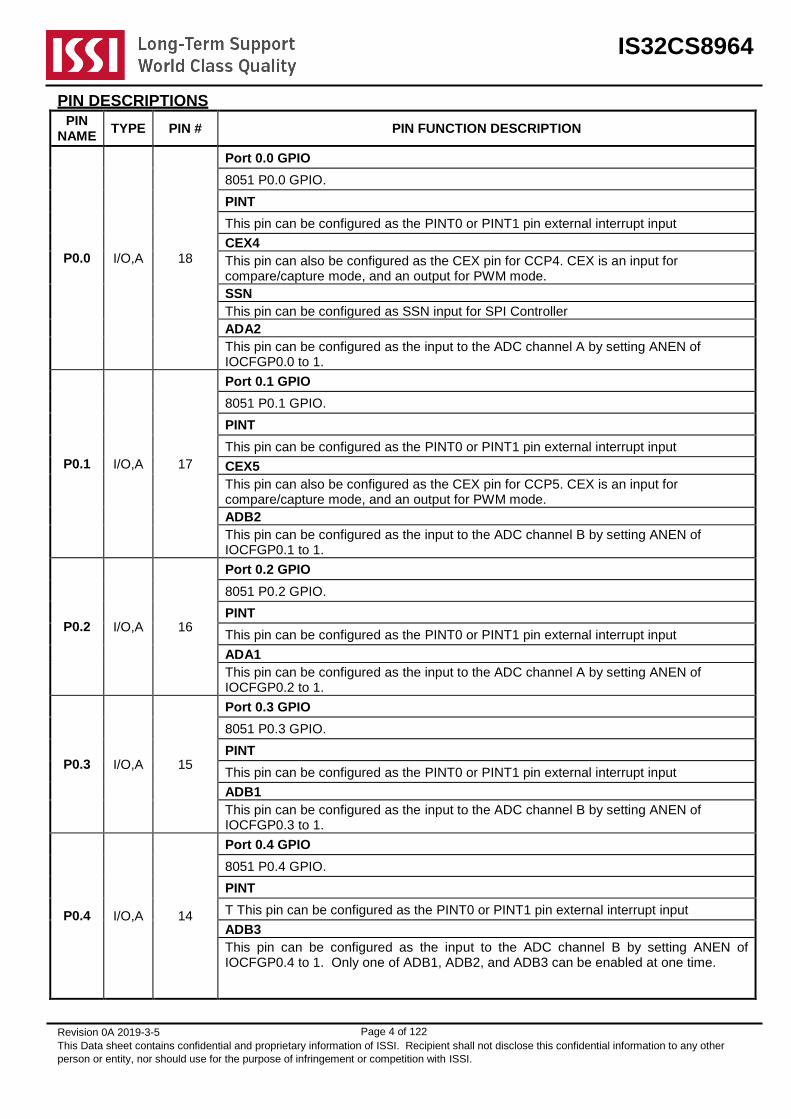
PIN DESCRIPTIONS
PIN NAME
TYPE PIN # PIN FUNCTION DESCRIPTION
P0.0 I/O,A 18
Port 0.0 GPIO
8051 P0.0 GPIO.
PINT
This pin can be configured as the PINT0 or PINT1 pin external interrupt input
CEX4
This pin can also be configured as the CEX pin for CCP4. CEX is an input for compare/capture mode, and an output for PWM mode.
SSN
This pin can be configured as SSN input for SPI Controller
ADA2
This pin can be configured as the input to the ADC channel A by setting ANEN of IOCFGP0.0 to 1.
P0.1 I/O,A 17
Port 0.1 GPIO
8051 P0.1 GPIO.
PINT
This pin can be configured as the PINT0 or PINT1 pin external interrupt input
CEX5
This pin can also be configured as the CEX pin for CCP5. CEX is an input for compare/capture mode, and an output for PWM mode.
ADB2
This pin can be configured as the input to the ADC channel B by setting ANEN of IOCFGP0.1 to 1.
P0.2 I/O,A 16
Port 0.2 GPIO
8051 P0.2 GPIO.
PINT
This pin can be configured as the PINT0 or PINT1 pin external interrupt input
ADA1
This pin can be configured as the input to the ADC channel A by setting ANEN of IOCFGP0.2 to 1.
P0.3 I/O,A 15
Port 0.3 GPIO
8051 P0.3 GPIO.
PINT
This pin can be configured as the PINT0 or PINT1 pin external interrupt input
ADB1
This pin can be configured as the input to the ADC channel B by setting ANEN of IOCFGP0.3 to 1.
P0.4 I/O,A 14
Port 0.4 GPIO
8051 P0.4 GPIO.
PINT
T This pin can be configured as the PINT0 or PINT1 pin external interrupt input
ADB3
This pin can be configured as the input to the ADC channel B by setting ANEN of IOCFGP0.4 to 1. Only one of ADB1, ADB2, and ADB3 can be enabled at one time.

IS32CS8964
Revision 0A 2019-3-5
This Data sheet contains confidential and proprietary information of ISSI. Recipient shall not disclose this confidential information to any other
person or entity, nor should use for the purpose of infringement or competition with ISSI.
Page 5 of 122
PIN NAME
TYPE PIN # PIN FUNCTION DESCRIPTION
P0.5 I/O,A 13
Port 0.5 GPIO
8051 P0.5 GPIO.
PINT
This pin can be configured as the PINT0 or PINT1 pin external interrupt input.
XEMG
This pin can also be configured as the XEMG input for PWM16. When XEMG is asserted, all PWM16 channel outputs are disabled.
ADA3
This pin can be configured as the input to the ADC channel A by setting ANEN of IOCFGP0.5 to 1.
P0.6 I/O,A 12
Port 0.6 GPIO
8051 P0.6 GPIO.
PINT
This pin can be configured as the PINT0 or PINT1 pin external interrupt input
TXD0
This pin can also be configured as the transmit output pin for UART0.
TXD2
This pin can also be configured as the transmit output pin for EUART2.
ADC2
This pin can be configured as the input to the ADC channel C by setting ANEN of IOCFGP0.6 to 1.
P0.7 I/O,A 11
Port 0.7 GPIO
8051 P0.6 GPIO.
PINT
This pin can be configured as the PINT0 or PINT1 pin external interrupt input
RXD0
This pin can also be configured as the receiving input pin for UART0.
RXD2
This pin can also be configured as the receiving input pin for EUART2.
ADD2
This pin can be configured as the input to the ADC channel D by setting ANEN of IOCFGP0.7 to 1.
P1.0 I/O,A 10
Port 1.0 GPIO
8051 P1.0 GPIO.
PINT
This pin can be configured as the PINT0 or PINT1 pin external interrupt input
PWNAP
This pin can be configured as PWM16 Channel A positive output
CEX0
This pin can also be configured as the CEX pin for CCP0. CEX is an input for compare/capture mode, and an output for PWM mode.
ADD3
This pin can be configured as the input to the ADC channel D by setting ANEN of IOCFGP1.0 to 1.
P1.1 I/O,A 9 Port 1.1 GPIO
8051 P1.1 GPIO.

IS32CS8964
Revision 0A 2019-3-5
This Data sheet contains confidential and proprietary information of ISSI. Recipient shall not disclose this confidential information to any other
person or entity, nor should use for the purpose of infringement or competition with ISSI.
Page 6 of 122
PIN NAME
TYPE PIN # PIN FUNCTION DESCRIPTION
PINT
This pin can be configured as the PINT0 or PINT1 pin external interrupt input
PWNAN
This pin can be configured as PWM16 Channel A negative output
CEX1
This pin can also be configured as the CEX pin for CCP1. CEX is an input for compare/capture mode, and an output for PWM mode.
ADD4
This pin can be configured as the input to the ADC channel D by setting ANEN of IOCFGP1.1 to 1.
P1.2 I/O,A 4
Port 1.2 GPIO
8051 P1.2 GPIO.
PINT
This pin can be configured as the PINT0 or PINT1 pin external interrupt input
SSDA1
This pin can be configured as I2CS1 SDA I/O. The IOCOFG must also be configured as Open-Drain and external pull up resistor connecting to VDD is necessary.
CEX2
This pin can also be configured as the CEX pin for CCP2. CEX is an input for compare/capture mode, and an output for PWM mode.
PWMAP
This pin can be configured as PWM16 Channel A positive output.
ADD7
This pin can be configured as the input to the ADC channel D by setting ANEN of IOCFGP1.2 to 1.
P1.3 I/O,A 3
Port 1.3 GPIO
8051 P1.3 GPIO.
PINT
This pin can be configured as the PINT0 or PINT1 pin external interrupt input
SSCL1
This pin can be configured as I2CS1 SCL I/O. The IOCOFG must also be configured as Open- Drain and external pull up resistor connecting to VDD is necessary.
CEX3
This pin can also be configured as the CEX pin for CCP3. CEX is an input for compare/capture mode, and an output for PWM mode.
PWMAN
This pin can be configured as PWM16 Channel A negative output.
ADD8
This pin can be configured as the input to the ADC channel D by setting ANEN of IOCFGP1.3 to 1.
P1.4 I/O,A 8
Port 1.4 GPIO
8051 P1.4 GPIO.
PINT
This pin can be configured as the PINT0 or PINT1 pin external interrupt input
SSCL2
This pin can be configured as I2CS2 SCL I/O. The IOCOFG must also be configured as Open- Drain and external pull up resistor connecting to VDD is necessary.
MSCL
IS32CS8964
Revision 0A 2019-3-5
This Data sheet contains confidential and proprietary information of ISSI. Recipient shall not disclose this confidential information to any other
person or entity, nor should use for the purpose of infringement or competition with ISSI.
Page 7 of 122
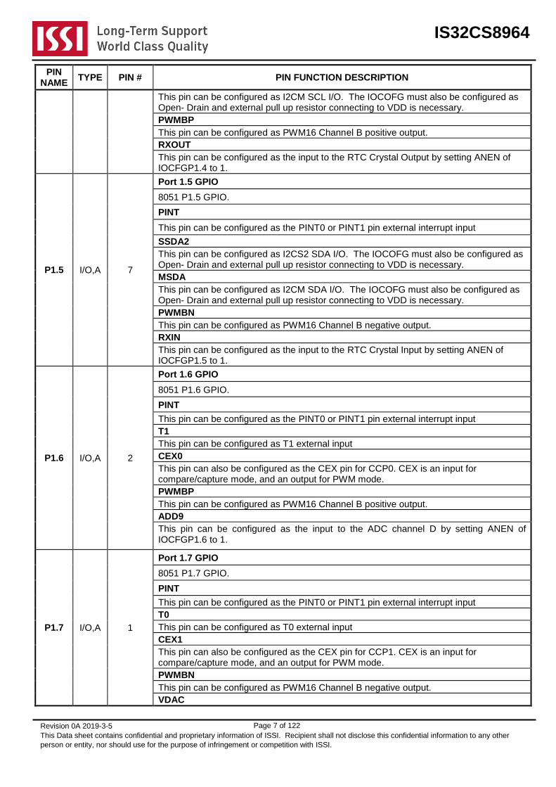
PIN NAME
TYPE PIN # PIN FUNCTION DESCRIPTION
This pin can be configured as I2CM SCL I/O. The IOCOFG must also be configured as Open- Drain and external pull up resistor connecting to VDD is necessary.
PWMBP
This pin can be configured as PWM16 Channel B positive output.
RXOUT
This pin can be configured as the input to the RTC Crystal Output by setting ANEN of IOCFGP1.4 to 1.
P1.5 I/O,A 7
Port 1.5 GPIO
8051 P1.5 GPIO.
PINT
This pin can be configured as the PINT0 or PINT1 pin external interrupt input
SSDA2
This pin can be configured as I2CS2 SDA I/O. The IOCOFG must also be configured as Open- Drain and external pull up resistor connecting to VDD is necessary.
MSDA
This pin can be configured as I2CM SDA I/O. The IOCOFG must also be configured as Open- Drain and external pull up resistor connecting to VDD is necessary.
PWMBN
This pin can be configured as PWM16 Channel B negative output.
RXIN
This pin can be configured as the input to the RTC Crystal Input by setting ANEN of IOCFGP1.5 to 1.
P1.6 I/O,A 2
Port 1.6 GPIO
8051 P1.6 GPIO.
PINT
This pin can be configured as the PINT0 or PINT1 pin external interrupt input
T1
This pin can be configured as T1 external input
CEX0
This pin can also be configured as the CEX pin for CCP0. CEX is an input for compare/capture mode, and an output for PWM mode.
PWMBP
This pin can be configured as PWM16 Channel B positive output.
ADD9
This pin can be configured as the input to the ADC channel D by setting ANEN of IOCFGP1.6 to 1.
P1.7 I/O,A 1
Port 1.7 GPIO
8051 P1.7 GPIO.
PINT
This pin can be configured as the PINT0 or PINT1 pin external interrupt input
T0
This pin can be configured as T0 external input
CEX1
This pin can also be configured as the CEX pin for CCP1. CEX is an input for compare/capture mode, and an output for PWM mode.
PWMBN
This pin can be configured as PWM16 Channel B negative output.
VDAC
IS32CS8964
Revision 0A 2019-3-5
This Data sheet contains confidential and proprietary information of ISSI. Recipient shall not disclose this confidential information to any other
person or entity, nor should use for the purpose of infringement or competition with ISSI.
Page 8 of 122
PIN NAME
TYPE PIN # PIN FUNCTION DESCRIPTION
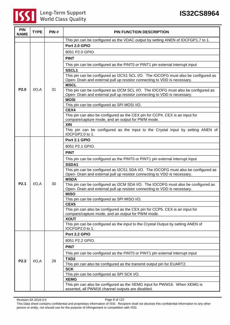
This pin can be configured as the VDAC output by setting ANEN of IOCFGP1.7 to 1.
P2.0 I/O,A 31
Port 2.0 GPIO
8051 P2.0 GPIO.
PINT
This pin can be configured as the PINT0 or PINT1 pin external interrupt input
SSCL1
This pin can be configured as I2CS1 SCL I/O. The IOCOFG must also be configured as Open- Drain and external pull up resistor connecting to VDD is necessary.
MSCL
This pin can be configured as I2CM SCL I/O. The IOCOFG must also be configured as Open- Drain and external pull up resistor connecting to VDD is necessary.
MOSI
This pin can be configured as SPI MOSI I/O.
CEX4
This pin can also be configured as the CEX pin for CCP4. CEX is an input for compare/capture mode, and an output for PWM mode.
XIN
This pin can be configured as the input to the Crystal Input by setting ANEN of IOCFGP2.0 to 1.
P2.1 I/O,A 30
Port 2.1 GPIO
8051 P2.1 GPIO.
PINT
This pin can be configured as the PINT0 or PINT1 pin external interrupt input
SSDA1
This pin can be configured as I2CS1 SDA I/O. The IOCOFG must also be configured as Open- Drain and external pull up resistor connecting to VDD is necessary.
MSDA
This pin can be configured as I2CM SDA I/O. The IOCOFG must also be configured as Open- Drain and external pull up resistor connecting to VDD is necessary.
MISO
This pin can be configured as SPI MISO I/O.
CEX5
This pin can also be configured as the CEX pin for CCP5. CEX is an input for compare/capture mode, and an output for PWM mode.
XOUT
This pin can be configured as the input to the Crystal Output by setting ANEN of IOCFGP2.0 to 1.
P2.2 I/O,A 29
Port 2.2 GPIO
8051 P2.2 GPIO.
PINT
This pin can be configured as the PINT0 or PINT1 pin external interrupt input
TXD2
This pin can also be configured as the transmit output pin for EUART2.
SCK
This pin can be configured as SPI SCK I/O.
XEMG
This pin can also be configured as the XEMG input for PWM16. When XEMG is asserted, all PWM16 channel outputs are disabled.

IS32CS8964
Revision 0A 2019-3-5
This Data sheet contains confidential and proprietary information of ISSI. Recipient shall not disclose this confidential information to any other
person or entity, nor should use for the purpose of infringement or competition with ISSI.
Page 9 of 122
PIN NAME
TYPE PIN # PIN FUNCTION DESCRIPTION
VDAC
This pin can be configured as the VDAC output by setting ANEN of IOCFGP2.2 to 1.
P2.3 I/O,A 28
Port 2.3 GPIO
8051 P2.3 GPIO.
PINT
This pin can be configured as the PINT0 or PINT1 pin external interrupt input
RXD2
This pin can also be configured as the receiving input pin for EUART2.
SSN
This pin can be configured as SPI SSN input.
XEMG
This pin can also be configured as the XEMG input for PWM16. When XEMG is asserted, all PWM16 channel outputs are disabled.
CMPTH
This pin can be configured as comparator external threshold by setting ANEN of IOCFGP2.3 to 1.
P2.4 I/O,A 27
Port 2.4 GPIO
8051 P2.4 GPIO.
PINT
This pin can be configured as the PINT0 or PINT1 pin external interrupt input
T2
This pin can be configured as T2 external input
PWMCP
This pin can be configured as PWM16 Channel C positive output.
CMPD
This pin can be configured as the comparator D input by setting ANEN of IOCFGP2.4 to 1.
P2.5 I/O,A 26
Port 2.5 GPIO
8051 P2.5 GPIO.
PINT
This pin can be configured as the PINT0 or PINT1 pin external interrupt input
CEX4
This pin can also be configured as the CEX pin for CCP4. CEX is an input for compare/capture mode, and an output for PWM mode.
PWMCN
This pin can be configured as PWM16 Channel C negative output.
CMPC
This pin can be configured as the comparator C input by setting ANEN of IOCFGP2.5 to 1.
P2.6 I/O,A 25
Port 2.6 GPIO
8051 P2.6 GPIO.
PINT
This pin can be configured as the PINT0 or PINT1 pin external interrupt input
CEX5
This pin can also be configured as the CEX pin for CCP5. CEX is an input for compare/capture mode, and an output for PWM mode.
SSN

IS32CS8964
Revision 0A 2019-3-5
This Data sheet contains confidential and proprietary information of ISSI. Recipient shall not disclose this confidential information to any other
person or entity, nor should use for the purpose of infringement or competition with ISSI.
Page 10 of 122
PIN NAME
TYPE PIN # PIN FUNCTION DESCRIPTION
This pin can be configured as SPI SSN input.
CMPB
This pin can be configured as the comparator B input by setting ANEN of IOCFGP2.6 to 1.
P2.7 I/O,A 24
Port 2.7 GPIO
8051 P2.7 GPIO.
PINT
This pin can be configured as the PINT0 or PINT1 pin external interrupt input
XEMG
This pin can also be configured as the XEMG input for PWM16. When XEMG is asserted, all PWM16 channel outputs are disabled.
SCK
This pin can be configured as SPI SCK I/O.
T2EX Timer 2 Trigger
This pin also can be configured as T2EX signal for Timer 2. T2EX is the Timer 2 trigger input.
CMPA
This pin can be configured as the comparator A input by setting ANEN of IOCFGP2.7 to 1.
P3.0 I/O,A 6
Port 3.0 GPIO
8051 P3.0 GPIO.
PINT
This pin can be configured as the PINT0 or PINT1 pin external interrupt input
CEX2
This pin can also be configured as the CEX pin for CCP2. CEX is an input for compare/capture mode, and an output for PWM mode.
PWMCN
This pin can be configured as PWM16 Channel C negative output.
ADD5
This pin can be configured as the input to the ADC channel D by setting ANEN of IOCFGP3.0 to 1.
P3.1 I/O,A 5
Port 3.0 GPIO
8051 P3.0 GPIO.
PINT
This pin can be configured as the PINT0 or PINT1 pin external interrupt input
CEX3
This pin can also be configured as the CEX pin for CCP3. CEX is an input for compare/capture mode, and an output for PWM mode.
PWMCP
This pin can be configured as PWM16 Channel C positive output.
ADD6
This pin can be configured as the input to the ADC channel D by setting ANEN of IOCFGP3.1 to 1.
P3.2 I/O,A 23
Port 3.2 GPIO
8051 P3.2 GPIO.
PINT
This pin can be configured as the PINT0 or PINT1 pin external interrupt input

IS32CS8964
Revision 0A 2019-3-5
This Data sheet contains confidential and proprietary information of ISSI. Recipient shall not disclose this confidential information to any other
person or entity, nor should use for the purpose of infringement or competition with ISSI.
Page 11 of 122
PIN NAME
TYPE PIN # PIN FUNCTION DESCRIPTION
CEX4
This pin can also be configured as the CEX pin for CCP4. CEX is an input for compare/capture mode, and an output for PWM mode.
TXD2
This pin can also be configured as the transmit output pin for EUART2.
MOSI
This pin can be configured as SPI MOSI I/O.
VDAC
This pin can be configured as the VDAC output by setting ANEN of IOCFGP3.2 to 1.
P3.3 I/O,A 22
Port 3.3 GPIO
8051 P3.3 GPIO.
PINT
This pin can be configured as the PINT0 or PINT1 pin external interrupt input
CEX5
This pin can also be configured as the CEX pin for CCP5. CEX is an input for compare/capture mode, and an output for PWM mode.
RXD2
This pin can also be configured as the receiving input pin for EUART2.
MISO
This pin can be configured as SPI MISOI I/O.
CMPA
This pin can be configured as the comparator A input by setting ANEN of IOCFGP3.3 to 1.
VSS G 32 Typical decoupling capacitors of 0.1uF and 4.7uF should be connected between VDDC and VSS.
VDDC P 19
Core Supply Voltage of on-chip 1.8V regulator output
A good decoupling capacitor between VDDC and VSS pins is critical for good performance. The decoupling capacitor also holds the stored charged during SLEEP mode. For extended period of SLEEP mode, a 4.7uF decoupling capacitor should be used.
VDD P 20
Supply Voltage input (2.5V – 5.5V)
VDD supplies power to I/O buffers as well as analog circuits such as ADC and comparators, and RTC oscillator. A good decoupling capacitor between VDD and VSS pins is critical for good performance.
RSTN I/O,A 21
Reset Low Active.
Typically connect a resistor to VDDC and a capacitor to VSS.
RSTN is pulled low actively when LVR occurs. The threshold of RSTN is set at 0.5VDDC. RSTN is also used for internal test mode when RSTN > VDDC + 1.0V.
Note: “P” denotes power supply pins
“G” denotes ground pins. All VSS pins are internally shorted resistively.
“O”, “IO”, “A” denotes output only, input/output, and analog types.
“PU” or “PD” denotes pins with internal pull-up or pull-down.

IS32CS8964
Revision 0A 2019-3-5
This Data sheet contains confidential and proprietary information of ISSI. Recipient shall not disclose this confidential information to any other
person or entity, nor should use for the purpose of infringement or competition with ISSI.
Page 12 of 122
MEMORY MAP
There are total 256 bytes internal RAM in IS32CS8964, the same as standard 8052. There are total 1792 bytes auxiliary RAM allocated in the 8051 extended RAM are at 0x0100h – 0x07FFh. Programs can use "MOVX" instruction to access the XRAM. The 64KB embedded flash occupies the code address space from 0x0000h – 0xFFFFh. The CPU reset to address 0xF000h. The memory map is shown in the following:
IRAMMOC A, Direct
Or
MOV A, @R
0x0000H
0x007FH
SFRMOV A, Direct
0x0080H
0x00FFH0x0100H
0x07FFH
RESERVED
0x0800H
0xA000H
0xAFFFH
RESERVED
0xB000H
0xFFFFH
XFRMOVX A, @DPTR
XRAMMOVX A, @DPTR
IRAMMOV A, @R
64K
EMBEDDED
FLASH
0x0000H
0xFFFFH
0xF000HRESET
DATA MEMORY
MAP
CODE MEMORY
MAP

IS32CS8964
Revision 0A 2019-3-5
This Data sheet contains confidential and proprietary information of ISSI. Recipient shall not disclose this confidential information to any other
person or entity, nor should use for the purpose of infringement or competition with ISSI.
Page 13 of 122
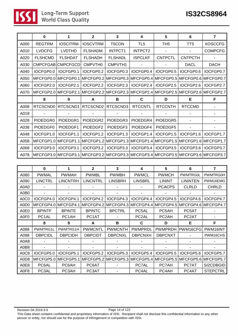
REGISTER MAP SFR(0x80 – 0xFF) and XFR (0xA000 – 0xAFFF)
The SFR address map maintains maximum compatibilities to most commonly used 8051 like MCU. The following table shows the SFR address map. Since SFR can be accessed by direct addressing mode, registers of built-in peripherals that require fast access are mostly located in SFR. XFR is mainly used for on-chip peripheral control and configurations.
0 1 2 3 4 5 6 7
0XF0 B - CLSR CHSR I2CMSA I2CMCR I2CMBUF I2CMTP
0XE0 ACC PCACON CCAP3L CCAP3H CCAP4L CCAP4H CCAP5L CCAP5H
0XD0 PSW PCAMOD CCAP0L CCAP0H CCAP1L CCAP1H CCAP2L CCAP2H
0XC0 - - SCON2 - PMR STATUS MCON TA
0XB0 P3 - CCAPM0 CCAPM1 CCAPM2 CCAPM3 CCAPM4 CCAPM5
0XA0 P2 SPICR SPIMR SPIST SPIDAT SFIFO2 SBUF2 SINT2
0X90 P1 EXIF WTST DPX CMPST DPX1 - -
0X80 P0 SP DPL DPH DPL1 DPH1 DPS PCON
8 9 A B C D E F
0XF8 EXIP MD0 MD1 MD2 MD3 MD4 MD5 ARCON
0XE8 EXIE CH MXAX I2CSCON1 I2CSST1 I2CSADR1 I2CSDAT1 P4
0XD8 WDCON CL DPXR I2CSCON2 I2CSST2 I2CSADR2 I2CSDAT2 P5
0XC8 T2CON TB RLDL RLDH TL2 TH2 ADCAVG T34CON
0XB8 IP ADCCHSL ADCAL ADCAH ADCBL ADCBH ADCCL ADCCH
0XA8 IE ADCCFG ADCDL ADCDH TL4 TH4 TL3 TH3
0X98 SCON0 SBUF0 - ESP - ACON I2CSADR3 WKMASK
0X88 TCON TMOD TL0 TL1 TH0 TH1 CKCON CKSEL
IS32CS8964
Revision 0A 2019-3-5
This Data sheet contains confidential and proprietary information of ISSI. Recipient shall not disclose this confidential information to any other
person or entity, nor should use for the purpose of infringement or competition with ISSI.
Page 14 of 122
0 1 2 3 4 5 6 7
A000 REGTRM IOSCITRM IOSCVTRM T5CON TL5 TH5 TT5 XOSCCFG
A010 LVDCFG LVDTHD FLSHADM INTPCT1 INTPCT2 - - COMPCFG
A020 FLSHCMD FLSHDAT FLSHADH FLSHADL ISPCLKF CNTPCTL CNTPCTH -
A030 CMPCFGAB CMPCFGCD CMPVTH0 CMPVTH1 - - DACL DACH
A040 IOCFGP0.0 IOCFGP0.1 IOCFGP0.2 IOCFGP0.3 IOCFGP0.4 IOCFGP0.5 IOCFGP0.6 IOCFGP0.7
A050 MFCFGP0.0 MFCFGP0.1 MFCFGP0.2 MFCFGP0.3 MFCFGP0.4 MFCFGP0.5 MFCFGP0.6 MFCFGP0.7
A060 IOCFGP2.0 IOCFGP2.1 IOCFGP2.2 IOCFGP2.3 IOCFGP2.4 IOCFGP2.5 IOCFGP2.6 IOCFGP2.7
A070 MFCFGP2.0 MFCFGP2.1 MFCFGP2.2 MFCFGP2.3 MFCFGP2.4 MFCFGP2.5 MFCFGP2.6 MFCFGP2.7
8 9 A B C D E F
A008 RTCSCND0 RTCSCND1 RTCSCND2 RTCSCND3 RTCCNTL RTCCNTH RTCCMD -
A018 - - - - - - - -
A028 PIOEDGR0 PIOEDGR1 PIOEDGR2 PIOEDGR3 PIOEDGR4 PIOEDGR5 - -
A038 PIOEDGF0 PIOEDGF1 PIOEDGF2 PIOEDGF3 PIOEDGF4 PIOEDGF5 - -
A048 IOCFGP1.0 IOCFGP1.1 IOCFGP1.2 IOCFGP1.3 IOCFGP1.4 IOCFGP1.5 IOCFGP1.6 IOCFGP1.7
A058 MFCFGP1.0 MFCFGP1.1 MFCFGP1.2 MFCFGP1.3 MFCFGP1.4 MFCFGP1.5 MFCFGP1.6 MFCFGP1.7
A068 IOCFGP3.0 IOCFGP3.1 IOCFGP3.2 IOCFGP3.3 IOCFGP3.4 IOCFGP3.5 IOCFGP3.6 IOCFGP3.7
A078 MFCFGP3.0 MFCFGP3.1 MFCFGP3.2 MFCFGP3.3 MFCFGP3.4 MFCFGP3.5 MFCFGP3.6 MFCFGP3.7
0 1 2 3 4 5 6 7
A080 PWMAL PWMAH PWMBL PWMBH PWMCL PWMCH PWMTRG0L PWMTRG0H
A090 LINCTRL LINCNTRH LINCNTRL LINSBRH LINSBRL LININT LININTEN PWM16EMG
A0A0 - - - - - PCACPS CLRLD CHRLD
A0B0 - - - - - - - -
A0C0 IOCFGP4.0 IOCFGP4.1 IOCFGP4.2 IOCFGP4.3 IOCFGP4.4 IOCFGP4.5 IOCFGP4.6 IOCFGP4.7
A0D0 MFCFGP4.0 MFCFGP4.1 MFCFGP4.2 MFCFGP4.3 MFCFGP4.4 MFCFGP4.5 MFCFGP4.6 MFCFGP4.7
A0E0 BPINTF BPINTE BPINTC BPCTRL PC5AL PC5AH PC5AT -
A0F0 PC1AL PC1AH PC1AT - PC2AL PC2AH PC2AT -
8 9 A B C D E F
A088 PWMTRG1L PWMTRG1H PWMCNTL PWMCNTH PWMPRDL PWMPRDH PWM16CFG PWM16INT
A098 DBPCIDL DBPCIDH DBPCIDT DBPCNXL DBPCNXH DBPCNXT - PWM16CHS
A0A8 - - - - - - - -
A0B8 - - - - - - - -
A0C8 IOCFGP5.0 IOCFGP5.1 IOCFGP5.2 IOCFGP5.3 IOCFGP5.4 IOCFGP5.5 IOCFGP5.6 IOCFGP5.7
A0D8 MFCFGP5.0 MFCFGP5.1 MFCFGP5.2 MFCFGP5.3 MFCFGP5.4 MFCFGP5.5 MFCFGP5.6 MFCFGP5.7
A0E8 PC6AL PC6AH PC6AT - PC7AL PC7AH PC7AT SI2CDBGID
A0F8 PC3AL PC3AH PC3AT - PC4AL PC4AH PC4AT STEPCTRL

IS32CS8964
Revision 0A 2019-3-5
This Data sheet contains confidential and proprietary information of ISSI. Recipient shall not disclose this confidential information to any other
person or entity, nor should use for the purpose of infringement or competition with ISSI.
Page 15 of 122
1. Enhanced 1-Cycle 8051 CPU
The CPU core is an enhanced version of standard 8051 used by series of ISSI’s MCU products. The CPU core is in RISC architecture and maintains binary instruction set compatible with the industry standard 8051. There is average 10 times performance enhancement in typical applications. The CPU operates at 20-bit addressing space that allows up to 1M bytes of program and data space for expansion. The CPU includes the following enhanced features compared with standard 8051:
16-bit LARGE addressing mode and 20-bit FLAT addressing mode control register ACON
Two data pointers DPTR and DPTR1, and additional DPS, DPX, DPX1, MXAX registers for MOVX instruction
8-bit stack pointer for LARGE mode and 16-bit extended stack pointer for FLAT mode control register ESP
Hardware Multiplication and Division Unit (MDU) provides 12 times faster performance using MD[5-0] and ARCON
Programmable wait state for program space for on-chip flash memory using WTST register
256 Bytes of Direct Data Memory
Enhanced Interrupt Controller allows 15 interrupt sources and 2 priority levels.
Power Saving modes include IDLE mode, Power Management mode (PMM), and STOP mode. The PMM mode also supports switchback features.
Access Control of critical registers - TA, and TB registers
Eight break pointers allows integration of common IDE
In addition to standard 8051 peripherals, the CPU core also integrates the following peripherals. These peripherals are in the same CPU clock domain.
Four 8-Bit I/O ports
16-bit Watch Dog Timer. WDT, WDCON, and CKCON registers
Three 16-bit Timers, T0/T1 and T2. TCON, RLDL, RLDH, TL2, TH2, and T2CON registers
UART0.
I2C Master Controller. I2CMSA, I2CMCR, I2CMBUF, and I2CMTP registers.
ALU
INTERRUPT
CONTROL
POWER
MANAGE
CLOCK
CONTROL
SFR
MEMORY
CONTROL
FLASH
CONTROLLER
SRAM
CONTROLLER
PROGRAM
SEQUENCER
AND DECODE
PORT
0/1/2/3
WDT
TIMER
0/1/2
I2C
MASTER
UART
0
EMBEDDED
FLASH MEMORY
ON-CHIP
SRAM
INT
ER
NA
L
OS
C
CPU CORE
XFR
OT
HE
R
PE
RIP
HE
RA
L
The following sections describe in detail these enhanced features and peripherals. Assuming readers are familiar with 8051 standard operations and peripherals, the compatible functions is not covered here.
IS32CS8964
Revision 0A 2019-3-5
This Data sheet contains confidential and proprietary information of ISSI. Recipient shall not disclose this confidential information to any other
person or entity, nor should use for the purpose of infringement or competition with ISSI.
Page 16 of 122
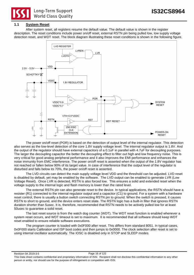
1.1 System Reset
After system reset, all registers resume the default value. The default value is shown in the register description. The reset conditions include power on/off reset, external RSTN pin being pulled low, low supply voltage detection reset, and WDT reset. The block diagram illustrating these reset conditions is shown in the following figure.
VDDC1.8V REGULATOR
VDDC*0.9
LVD REGISTER
LVDTH
LVREN
RSTNWDT RESET
SYSTEM
RESET
VTH=0.5*VDDC
POR
POWER-ON
RESET
VDD2.5V – 5.5V
SCHOTTKY
VDDC*0.7
LVR
RST
256 IOSC
CLK
EXTENSION
The power on/off reset (POR) is based on the detection of output level of the internal regulator. This detection also serves as the low-level detection of the core 1.8V supply voltage level. The internal regulator output is 1.8V. And the output of the regulator should have external capacitors of a 0.1uF in parallel with 4.7uF for decoupling purposes. The larger the decoupling capacitor the better the decoupling effect to filter out high and low frequency noise. This is very critical for good analog peripheral performance and it also improves the EMI performance and enhances the noise immunity from EMC interference. The power on/off reset is asserted when the output of the 1.8V regulator has not reached or fallen below 90% of its target value. In case of interference that the output level of the regulator is disturbed and falls below its 70%, the power on/off reset is asserted.
The LVD circuits can detect the main supply voltage level VDD and the threshold can be adjusted. LVD reset is disabled by default, yet may be enabled by the software. The LVD output can be enabled to generate LVR (Low Voltage Reset). Once LVR is detected, RSTN is also forced low. This ensures a solid and extended reset when the voltage supply to the internal logic and flash memory is lower than the rated level.
The external RSTN pin can also generate reset to the device. In typical applications, the RSTN should have a resister (R1) connected to the internal regulator output and a capacitor (C1) to ground. For a system with a hardware reset control, there is usually a button switch connecting RSTN pin to ground. When the switch is pressed, it causes RSTN to short to ground, and the device enters reset state. The RSTN logic has a built-in filter that ignores RSTN duration shorter than 5usec. It is, therefore, recommended that RSTN needs to be actively pulled low for at least 50usec to guarantee a solid reset.
The last reset source is from the watch dog counter (WDT). The WDT reset function is enabled whenever a system reset occurs, and WDT timeout is set to maximum. It is recommended that all software should keep WDT reset enabled to ensure reliable software executions.
The program counter is loaded with 0x0F000 after reset. This differs from standard 8051. In typical cases, 0x0F000 starts Calibration and ISP boot codes and then jumps to 0x0000. The clock selection after reset is set to using internal oscillator automatically. The IOSC is disabled only in STOP and SLEEP modes.

IS32CS8964
Revision 0A 2019-3-5
This Data sheet contains confidential and proprietary information of ISSI. Recipient shall not disclose this confidential information to any other
person or entity, nor should use for the purpose of infringement or competition with ISSI.
Page 17 of 122
1.2 CPU Registers
ACC (0xE0) Accumulator R/W (0x00)
7 6 5 4 3 2 1 0
RD ACC[7-0]
WR ACC[7-0]
ACC is the CPU accumulator register and is involved in direct operations of many instructions. ACC is bit addressable.
B (0xF0) B Register R/W (0x00)
7 6 5 4 3 2 1 0
RD B[7-0]
WR B[7-0]
B register is used in standard 8051 multiply and divide instructions and also used as an auxiliary register for temporary storage. B is also bit addressable.
PSW (0xD0) Program Status Word R/W (0x00)
7 6 5 4 3 2 1 0
RD CY AC FO RS1 RS0 OV UD P
WR CY AC FO RS1 RS0 OV UD P
CY Carry Flag
AC Auxiliary Carry Flag (BCD Operations)
F0 General Purpose
RS1,RS0 Register Bank Select
OV Overflow Flag
UD User Defined (reserved)
P Parity Flag
SP (0x81) Stack Pointer R/W (0x00)
7 6 5 4 3 2 1 0
RD SP[7-0]
WR SP[7-0]
PUSH will result ACC to be written to SP+1 address. POP will load ACC from IRAM with the address of SP.
ESP (0x9B) Extended Stack Pointer R/W (0x00)
7 6 5 4 3 2 1 0
RD ESP[7-0]
WR ESP[7-0]
In FLAT address mode, ESP and SP together form a 16-bit address for stack pointer. ESP holds the higher byte of the 16-bit address.
1.3 Addressing Mode and Memory Operations
The LARGE mode, addressing mode is compatible with standard 8051 in 16-bit address. FLAT mode extends the program address to 20-bit and expands the stack space to 16-bit data space. The data space is always 16-bit in either LARGE or FLAT mode.
ACON (0x9D) R/W (0x00) TA
7 6 5 4 3 2 1 0
RD - - - - DPXREN SA AM1 AM0
WR - - - - DPXREN SA AM1 AM0
ACON is addressing mode control register.
DPXREN DPXR Register Control Bit.
IS32CS8964
Revision 0A 2019-3-5
This Data sheet contains confidential and proprietary information of ISSI. Recipient shall not disclose this confidential information to any other
person or entity, nor should use for the purpose of infringement or competition with ISSI.
Page 18 of 122
If DPXREN is 0, “MOVX, @Ri” instruction uses P2 (0xA0) register and XRAM Address [15-8]. If DPXREN is 1 DPXR (0xDA) register and XRAM Address [15-8] is used .
SA Extended Stack Address Mode Indicator. This bit is read-only.
0 – 8051 standard stack mode where stack resides in internal 256-byte memory
1 – Extended stack mode. Stack pointer is ESP:SP in 16-bit addressing to data space.
AM1, AM0 AM1 and AM0 Address Mode Control Bits
00 – LARGE address mode in 16-bit
1x – FLAT address mode with 20-bit program address
DPXR (0xDA) R/W (0x00)
7 6 5 4 3 2 1 0
RD DPXR[7-0]
WR DPXR[7-0]
DPXR[7-0] is used to repplace P2[7-0] for high byte of XRAM address for ”MOVX, @R1” or ”MOVX, @R0” when DPXREN=1.
The clock speed of an MCU with embedded flash memory is usually limited by the access time of on-chip flash memory. While in modern process technology, the CPU can operate up to 100MHz to 200MHz, but the access time of flash memory is usually around 20 nanoseconds and thus limiting the clock rate to lower than 50MHz. To alleviate this problem, a programmable wait state function is incorporated to allow faster CPU clock rate however slower embedded flash memory. The wait state is controlled by WTST register as shown in the following,
WTST (0x92) R/W (0x07)
7 6 5 4 3 2 1 0
RD - - - - WTST3 WTST2 WTST1 WTST0
WR - - - - WTST3 WTST2 WTST1 WTST0
WTST is wait state register that controls the program access wait state only.

IS32CS8964
Revision 0A 2019-3-5
This Data sheet contains confidential and proprietary information of ISSI. Recipient shall not disclose this confidential information to any other
person or entity, nor should use for the purpose of infringement or competition with ISSI.
Page 19 of 122
WTST[3-0] Wait State Control register. WTST sets the wait state in CPU clock period
WTST3 WTST2 WTST1 WTST0 Wait State Cycle
0 0 0 0 1
0 0 0 1 2
0 0 1 0 3
0 0 1 1 4
0 1 0 0 5
0 1 0 1 6
0 1 1 0 7
0 1 1 1 8
1 0 0 0 9
1 0 0 1 10
1 0 1 0 11
1 0 1 1 12
1 1 0 0 13
1 1 0 1 14
1 1 1 0 15
1 1 1 1 16
The default setting of the program wait state register after reset is 0x07 and the software must initialize the setting to change the wait state setting. For typical embedded flash, the read access time is specified as 40 nsec. Therefore the user should set the WTST register according to the SYSCLK frequency. For example, using a SYSCLK of 4MHz, the WTST can be set to minimum because one clock period is 250 nsec which is longer than the embedded flash access time. If SYSCLK is above 16MHz, then WTST should be set higher than 1 to allow enough read access time.
1.4 Dual Data Pointers and MOVX operations
In standard 8051/8052, there is only one data pointers DPH:DPL to perform MOVX. The enhanced CPU provides 2
nd data pointer DPH1:DPL1 to speed up the movement, or copying of data block. The active DPTR is
selected and operation of DPTR is controlled by setting DPS (Data Pointer Select) register. Through the control DPS, efficient programming can be achieved.
DPS (0x86) R/W (0x00)
7 6 5 4 3 2 1 0
RD ID1 ID0 TSL - - - - SEL
WR ID1 ID0 TSL - - - - SEL
ID[1:0] Define the operation of Increment/Decrement functions of selected DPTR for INC DPTR instruction is executed.
ID1 ID0 SEL=0 SEL=1
0 0 INC DPTR INC DPTR1
0 1 DEC DPTR INC DPTR1
1 0 INC DPTR DEC DPTR1
1 1 DEC DPTR DEC DPTR1
TSL Enable toggling selection of DPTR selection. When this bit is set, the selection of DPTR is toggled when DPTR is used in an instruction and executed.
SEL DPTR selection bit. Set to select DPTR1, and clear to select DPTR. SEL is also affected by the state of ID[1:0] and TSL after DPTR is used in an instruction. When read, SEL reflects the current selection of command.

IS32CS8964
Revision 0A 2019-3-5
This Data sheet contains confidential and proprietary information of ISSI. Recipient shall not disclose this confidential information to any other
person or entity, nor should use for the purpose of infringement or competition with ISSI.
Page 20 of 122
DPL (0x82) Data Pointer Low R/W (0x00)
7 6 5 4 3 2 1 0
RD DPL[7-0]
WR DPL[7-0]
DPL register holds the low byte of data pointer, DPTR.
DPH (0x83) Data Pointer High R/W (0x00)
7 6 5 4 3 2 1 0
RD DPH[7-0]
WR DPH[7-0]
DPH register holds the high byte of data pointer, DPTR.
DPL1 (0x84) Extended Data Pointer Low R/W (0x00)
7 6 5 4 3 2 1 0
RD DPL1[7-0]
WR DPL1[7-0]
DPL1 register holds the low byte of extended data pointer 1, DPTR1.
DPH1 (0x85) Extended Data Pointer High R/W (0x00)
7 6 5 4 3 2 1 0
RD DPH1[7-0]
WR DPH1[7-0]
DPH1 register holds the high byte of extended data pointer 1, DPTR1.
DPX (0x93) Data Pointer Top R/W (0x00)
7 6 5 4 3 2 1 0
RD DPX[7-0]
WR DPX[7-0]
DPX is used to provide top 8-bit address of DPTR when address above 64KB. The lower 16-bit address is formed by DPH and DPL. Since IS32CS8964 only has on-chip data RAM space, DPX value has no effect.
DPX1 (0x95) Extended Data Pointer Top R/W (0x00)
7 6 5 4 3 2 1 0
RD DPX1[7-0]
WR DPX1[7-0]
DPX1 is used to provide top 8-bit address of DPTR when address above 64KB. The lower 16-bit address is formed by DPH and DPL. Since IS32CS8964 only has on-chip data RAM space, DPX value has no effect.
MXAX (0xEA) MOVX Extended Address Register R/W (0x00)
7 6 5 4 3 2 1 0
RD MXAX[7-0]
WR MXAX[7-0]
MXAX is used to provide top 8-bit address for an “MOVX @R0” or “MOVX @R1” instruction. The lower 16-bit address is formed by P2 and R0/R1 (if DPXREN=0), or formed by DPXR and R0/R1 (if DPXREN=1).
MCON (0xC6) XRAM Relocation Register R/W (0x00) TA Protected
7 6 5 4 3 2 1 0
RD MCON[7-0]
WR MCON[7-0]
IS32CS8964
Revision 0A 2019-3-5
This Data sheet contains confidential and proprietary information of ISSI. Recipient shall not disclose this confidential information to any other
person or entity, nor should use for the purpose of infringement or competition with ISSI.
Page 21 of 122
MCON holds the starting address of XRAM in 4KB steps. For example, if MCON[7-0]=0x01, the starting address is 0x001000h. MCON is not meaningful in IS32CS8964 because it only contains on-chip XRAM and MCON should not be modified from 0x00.
When accessing XRAM using “MOVX, @DPTR” instruction, the address of XRAM access is formed by DPHi:DPLi depending on which data pointer is selected. Another form of MOVX instruction is “MOVX, @Ri”. This instruction provides an efficient programming method to move content within a 256 byte data block. In “@RI” instruction, the XRAM address [15-7] can be derived from two sources. If ACON.DPXREN = 0, the high order address [15-8] is from P2 (0xA0), if ACON.DPXREN = 1, the high order address is from DPXR (0xDA) register.
The maximum addressing space of XRAM is up to 16MB thus requiring 24 bit address. For “MOVX, @DPTR”, the XRAMADDR [23-16] is from either DPX (0x93) or DPX1 (0x95) depending on which data pointer is selected. For “MOVX, @Ri”, the XRAMUADDR [23-16] is from MXAX (0xEA) register.
1.5 Interrupt System
The CPU implements an enhanced Interrupt Control that allows total 15 interrupt sources and each with two programmable priority levels. The interrupts are sampled at rising edge of SYSCLK. If interrupts are present and enabled, the CPU enters interrupt service routine by vectoring to the highest priority interrupt. Of the 15 interrupt sources, 7 of them are from CPU internal integrated peripherals, 6 of them are for on-chip external peripherals, and 2 of them are used for external pin interrupt expansion. When an interrupt is shared, the interrupt service routine must determine which source is requesting the interrupt by examining the corresponding interrupt flags of sharing peripherals.
The following table shows the interrupt sources and corresponding interrupt vectors. The Flag Reset column shows whether the corresponding interrupt flag is cleared by hardware (self-cleared) or software. Please note the software can only clear the interrupt flag but not set the interrupt flag. The Natural Priority column shows the inherent priority if more than one interrupts are assigned to the same priority level. Please note that the interrupts assigned with higher priority levels always get serviced first compared with interrupts assigned with lower priority levels regardless of the natural priority sequence.
Interrupt Peripheral Source Description Vectors FLAG RESET Natural Priority
PINT0 Expanded Pin INT0.x 0x03 Software 1
TF0 Timer 0 0x0B Hardware 2
PINT1 Expanded Pin INT1.x 0x13 Software 3
TF1 Timer 1 0x1B Hardware 4
TI0/RI0 UART0 0x23 Software 5
TF2 Timer 2 0x2B Software 6
TI2/RI2 EUART2/LIN 0x33 Software 7
I2CM I2C Master 0x3B Software 8
INT2 LVT/LVT18 0x43 Software 9
INT3 Comparator/EMG 0x4B Software 10
INT4 ADC (A-D) 0x53 Software 11
WDIF Watchdog 0x5B Software 12
INT6 PCA/CAPP/PWM16 0x63 Software 13
INT7 SPI/I2CS1/I2CS2 0x6B Software 14
INT8 RTC/Timer 3/Timer 4/Timer 5 0x73 Software 15
BKP Break Point 0x7B Software 0
DBG I2CS Debug 0x83 Software 0
In addition to the 15 peripheral interrupts, there are two highest priority interrupts associated with debugging and break point. DBG interrupt is generated when I
2C slave is configured as a debug port and a debug request from
the host matches the debug ID. BKP interrupt is generated when break point match condition occurs. DBG has higher priority than BKP. The BKP and DBG interrupts are not affected by global interrupt enable, EA bit, IE register (0xA8).

IS32CS8964
Revision 0A 2019-3-5
This Data sheet contains confidential and proprietary information of ISSI. Recipient shall not disclose this confidential information to any other
person or entity, nor should use for the purpose of infringement or competition with ISSI.
Page 22 of 122
The following diagram shows the interrupt sources and the expanded pin interrupts
PINT0EN[0]PINT0FG[0]PINT00
PINT0EN[1]PINT0FG[1]PINT01
IE[7] (EA)IE[0] (EINT0)
TCON[1] (IE0)
PINT1EN[0]PINT1[FG[0]PINT10
PINT1EN[1]PINT1FG[1]PINT11
PINT1EN[2]PINT1FG[2]PINT12
PINT1EN[3]PINT1FG[3]PINT13
PINT1EN[4]PINT1FG[4]PINT14
PINT1EN[5]PINT1FG[5]PINT15
IE[7] (EA)IE[2] (EINT1)TCON[3] (IE1)
IE[7] (EA)IE[1] (ET0)
TCON[5] (TF0)
IE[7] (EA)IE[3] (ET1)
TCON[7] (TF1)
SCON0[0] (RI0)SCON0[1] (TI0)
IE[7] (EA)IE[4] (ES0)
IE[7] (EA)EXIE[0]
EXIF[0] (I2CMIF)
IE[7] (EA)EXIE[1] (EINT2)EXIF[1] (INT2F)
CMPCFGAB[5] (INTENA)COMST[4] (CMPIFA)
LVDCFG[5] (LVTEN)LVDCFG[0] (LVTIF)
CMPCFGAB[1] (INTENB)COMST[5] (CMPIFB)
CMPCFGCD[5] (INTENC)COMST[6] (CMPIFC)
CMPCFGCD[1] (INTEND)COMST[7] (CMPIFD)
IE[7] (EA)EXIE[2] (EINT3)EXIF[2] (INT3F)
ADCCHSL[3] (CHAIF)ADCCFG[5] (ADCINTE)
ADCCHSL[2] (CHBIF)ADCCHSL[1] (CHCIF)ADCCHSL[0] (CHDIF)
IE[7] (EA)EXIE[3] (EINT4)EXIF[3] (INT4F)
IE[7] (EA)EXIE[4] (EWDI)
CMOD[0] (ECF)CCON[7] (CF)
CCAPM0[0] (ECCF)CCON[0] (CCF0)
CCAPM1[0] (ECCF)CCON[1] (CCF1)
CCAPM2[0] (ECCF)CCON[2] (CCF2)
CCAPM3[0] (ECCF)CCON[3] (CCF3)
CCAPM4[0] (ECCF)CCON[4] (CCF4)
CCAPM5[0] (ECCF)CCON[5] (CCF5)
IE[7] (EA)EXIE[5] (EINT6)
IE[7] (EA)EXIE[6] (EINT7)
SPICR[7] (SPIE)SPIST[7] (SPIINT)
CECCFG[4] (ETMOUTI)CECSTS[4] (TMOUTIF)
CECCFG[3] (ELNERRI)CECSTS[3] (LNERRIF)
CECCFG[2] (ETXERRI)CECSTS[2] (TXERRIF)
CECCFG[1] (ETXI)CECSTS[1] (TXIF)
CECCFG[0] (ERXI)
RTCCMD[7] (SECINTEN)RTCCMD[5] (SECINT)
RTCCMD[6] (ALMINTEN)RTCCMD[4] (ALMINT)
RTCCMD[3] (4HZINTEN)RTCCMD[2] (4HZINT)
IE[7] (EA)EXIE[7] (EINT8)
Interrupt to [ 0x03 ]
Interrupt to [ 0x0B ]
Interrupt to [ 0x13 ]
Interrupt to [ 0x1B ]
Interrupt to [ 0x23 ]
Interrupt to [ 0x3B ]
Interrupt to [ 0x43 ]
Interrupt to [ 0x4B ]
IE[7] (EA)IE[5] (ET2)
T2CON[7] (TF2)
SCON1[0] (RI1)SCON1[1] (TI1)
IE[7] (EA)IE[6] (ES1)
Interrupt to [ 0x2B ]
Interrupt to [ 0x33 ]
Interrupt to [ 0x53 ]
Interrupt to [ 0x5B ]
Interrupt to [ 0x63 ]
Interrupt to [ 0x6B ]
Interrupt to [ 0x73 ]
I2CSCON1[6] (EADDRMI)I2CSST1[6] (ADDRMI)
I2CSCON1[5] (ESTOPI)I2CSST1[5] (STOPI)
I2CSCON1[4] (ERPSTARTI)I2CSST1[4] (RPSTARTI)
I2CSCON1[3] (ETXBI)I2CSST1[3] (TXBI)
I2CSCON1[2] (ERCBI)I2CSST1[2] (RCBI)
I2CSCON2[6] (EADDRMI)I2CSST2[6] (ADDRMI)
I2CSCON1[5] (ESTOPI)I2CSST2[5] (STOPI)
I2CSCON1[4] (ERPSTARTI)I2CSST2[4] (RPSTARTI)
I2CSCON2[3] (ETXBI)I2CSST2[3] (TXBI)
I2CSCON2[2] (ERCBI)I2CSST2[2] (RCBI)
The interrupt related registers are listed in the following. Each interrupt can be individually enabled or disabled by setting or clearing corresponding bits in IE, EXIE and integrated peripherals’ control registers.
IE (0xA8) R/W (0x00)
7 6 5 4 3 2 1 0
RD EA ES2 ET2 ES0 ET1 PINT1EN ET0 PINT0EN
WR EA ES2 ET2 ES0 ET1 PINT1EN ET0 PINT0EN

IS32CS8964
Revision 0A 2019-3-5
This Data sheet contains confidential and proprietary information of ISSI. Recipient shall not disclose this confidential information to any other
person or entity, nor should use for the purpose of infringement or competition with ISSI.
Page 23 of 122
EA Global Interrupt Enable bit.
ES2 LIN-capable 16550-like UART2 Interrupt Enable bit.
ET2 Timer 2 Interrupt Enable bit.
ES0 UART0 Interrupt Enable bit.
ET1 Timer 1 Interrupt Enable bit.
PINT1EN Pin PINT1.x Interrupt Enable bit.
ET0 Timer 0 Interrupt Enable bit.
PINT0EN Pin PINT0.x Interrupt Enable bit.
EXIE (0xE8) R/W (0x00)
7 6 5 4 3 2 1 0
RD EINT8 EINT7 EINT6 EWDI EINT4 EINT3 EINT2 EI2CM
WR EINT8 EINT7 EINT6 EWDI EINT4 EINT3 EINT2 EI2CM
EINT8 RTC Interrupt Enable and Timer 3 Interrupt Enable bit.
EINT7 SPI and I2C Slave Interrupt Enable bit.
EINT6 PCA Interrupt Enable bit.
EWDI Watchdog Timer Interrupt Enable bit.
EINT4 ADC/PWM Interrupt Enable bit.
EINT3 Analog Comparator Interrupt and CAN Interrupt Enable bit.
EINT2 Low Voltage Detection Interrupt Enable bit.
EI2CM I2C Master Interrupt Enable bit.
Each interrupt can be individually assigned to either high or low. When the corresponding bit is set to 1, it indicates it is of high priority.
IP (0xB8) R/W (0x00)
7 6 5 4 3 2 1 0
RD - PS2 PT2 PS0 PT1 PX1 PT0 PX0
WR - PS2 PT2 PS0 PT1 PX1 PT0 PX0
PS2 LIN-capable 16550-like UART2 Priority bit.
PT2 Timer 2 Priority bit.
PS0 UART 0 Priority bit.
PT1 Timer 1 Priority bit.
PX1 Pin Interrupt INT1 Priority bit.
PT0 Timer 0 Priority bit.
PX0 Pin Interrupt INT0 Priority bit.
EXIP (0xF8) R/W (0x00)
7 6 5 4 3 2 1 0
RD EINT8 EINT7 EINT6 EWDI EINT4 EINT3 EINT2 EI2CM
WR EINT8 EINT7 EINT6 EWDI EINT4 EINT3 EINT2 EI2CM
EINT8 INT8 RTC Priority and Timer 3 Priority bit.
EINT7 INT7 SPI and I2C Slave Priority bit.
EINT6 INT6 PCA Priority bit.
EWDI Watchdog Priority bit.
EINT4 INT4 ADC/PWM Priority bit.
EINT3 INT3 Analog Comparator and CAN Controller Priority bit.
EINT2 INT2 Low Voltage Detection Priority bit.
EI2CM I2C Master Priority bit.

IS32CS8964
Revision 0A 2019-3-5
This Data sheet contains confidential and proprietary information of ISSI. Recipient shall not disclose this confidential information to any other
person or entity, nor should use for the purpose of infringement or competition with ISSI.
Page 24 of 122
EXIF (0x91) R/W (0x00)
7 6 5 4 3 2 1 0
RD INT8F INT7F INT6F - INT4F INT3F INT2F I2CMIF
WR - - - - - - - I2CMIF
INT8F INT8 RTC and Timer 3 Interrupt Flag bit
INT7F INT7 SPI and I2C Slave interrupt Flag bit
INT6F INT6 PCA Interrupt Flag bit
INT4F INT4 ADC/PWM Interrupt Flag bit
INT3F INT3 Analog Comparator Interrupt and CAN Interrupt Flag bit
INT2F INT2 Low Voltage Detection Interrupt Flag bit
I2CMIF I2C Master Interrupt Flag bit. This bit must be cleared by software
*** Writing to INT2F to INT8F has no effect.
The interrupt flag of internal peripherals are stored in the corresponding flag registers in the peripheral and EXIF registers. These peripherals include T0, T1, T2, and WDT. Therefore to clear the interrupt flags the software needs to clear the corresponding flags located in the peripherals (for T0, T1, and T2, and WDT). For I2CM, the interrupt flag is located in the EXIF register bit I2CMIF. This needs to be cleared by software.
INT2 to INT8 are used to connect to the external peripherals. INT2F to INT8F are direct equivalents of the interrupt flags from the corresponding peripherals. These peripherals include RTC, I
2Cs, PCA, ADC etc. Take RTC for
example; there are interrupt flags (SECINT, ALMINT, and 4HZINT) in RTCCMD register. The RTC interrupt is connected to INT8. When either one or more of SECINT, ALMINT, and 4HZINT of RTC is set, i.e., INT8F = (SECINT + ALMINT + 4HZINT), INT8F is set to 1. Software is required for clearing the origin of the interrupt flag in the RTC before exiting the service routine. In this example, if the service routine only clears one interrupt flag, i.e. SECINT but not ALMINT. After exiting, INT8F is still set and results in a re-entry of the interrupt service routine and then the service routine can take care of ALMINT.
PINT0 and PINT1 are used for external GPIO pin Interrupts. All GPIO pin can be enabled to generate the PINT0 or PINT1 depending on its MFCFG register setting. Each GPIO pin also contains the rising/falling edge detections and either or both edges can be used for interrupt triggering. The same signaling can be used for generating wake-up.
TCON (0x88) R/W (0x00)
7 6 5 4 3 2 1 0
RD TF1 TR1 TF0 TR0 PINT1F PINT1EG PINT0F PINT0EG
WR TF1 TR1 TF0 TR0 PINT1F PINT1EG PINT0F PINT0EG
TF1 Timer 1 Interrupt Flag bit. TF1 is cleared by hardware when entering the interrupt routine. TF1 can also be cleared by software.
TR1 Timer 1 Run Control bit. Set to enable Timer 1, and clear to disable Timer 1.
TF0 Timer 0 Interrupt Flag bit. TF0 is cleared by hardware when entering the interrupt routine. TF0 can also be cleared by software.
TR0 Timer 0 Run Control bit. Set to enable Timer 0, and clear to disable Timer 0.
PINT1F Pin INT1 Interrupt Flag bit. PINT1F is set to 1 by hardware when pin interrupt occurs. This must be cleared by software.
PINT1EG Pin Interrupt 1 Edge or Level Setting. PINT1EG=0 use level interrupt, and PINT1EG=1 use edge interrupt. In current implementations, PINT1EG must be set to 0 to ensure capture of interrupt.
PINT0F Pin INT0 Interrupt Flag bit. PINT0F is set to 1 by hardware when pin interrupt occurs. This must be cleared by software.
PINT0EG Pin Interrupt 0 Edge or Level Setting. PINT0EG=0 use level interrupt, and PINT0EG=1 use edge interrupt. In current implementations, PINT0EG must be set to 0 to ensure capture of interrupt.
1.6 Register Access Control
One important aspect of the embedded MCU is its reliable operations under a harsh environment. Many system failures results from the accidental loss of data or changes of critical registers that may lead to catastrophic effects. The CPU provides several protection mechanisms which are described in this section.

IS32CS8964
Revision 0A 2019-3-5
This Data sheet contains confidential and proprietary information of ISSI. Recipient shall not disclose this confidential information to any other
person or entity, nor should use for the purpose of infringement or competition with ISSI.
Page 25 of 122
TA (0xC7) Time Access A Control Register2 WO xxxxxxx0
7 6 5 4 3 2 1 0
RD - - - - - - - TASTAT
WR TA Register
TA access control emulates a ticket that must be purchased before modifying a critical register. To modify or write into a TA protected register, TA must be accessed in a predefined sequence to obtain the ticket. The ticket is used when an intended modification operation is done to the TA protected register. To obtain the next access a new ticket must be obtained again by performing the same predefined sequence on TA. TA does not limit the read access of the TA protected registers. The TA protected register includes WDCON (0xD8), MCON (0xC6), and ACON (0x9D) registers. The following predefined sequence is required to modify the content of MCON.
MOV TA, #0xAA;
MOV TA, #0x55;
MOV MCON, #0x01;
Once the access is granted, there is no time limitation of the access. The access is voided if any operation is performed in TA address. When read, the bit of TA indicates whether TA is locked or not (1 indicates “unlock” and 0 indicates “lock”).
TB (0xC9) Time Access B Control Register2 RW (0x00)
7 6 5 4 3 2 1 0
RD - - - - - - - TBSTAT
WR TB Register
TB access control functions are similar to TA control, except the ticket is for multiple uses with a time limit. Once access is granted, the access is open for 256 clock periods and then expires. The software can also read TB address to obtain the current TB status. The TB protected registers include two SFR registers, CKSEL (0x8F) and WKMASK (0x9F), and twelve XFR registers lodging REGTRM (0xA000), IOSCITRM (0xA001), IOSCVTRM (0xA002), XOSCCFG (0xA007), LVDCFG (0xA010), LVDTHD (0xA011), CNTPCTL (0xA025), CNTPCTH (0xA026), INTPCT1 (0xA013), INTPCT2 (0xA014), BPINTE (0xA0E1), and SI2C_DebugID (0xA0EF). To modify registers with TB protection, the following procedure must be performed.
MOV TB, #0xAA
MOV TB, #0x55
This action creates a timed window of 256 SYSCLK periods to allow write access of these TB protected registers. If any afore-mentioned operation sequences are repeated before the 128 cycles expires, a new 128 cycles is extended. The current 256 cycles can be terminated immediately by writing #0x00 to TB registers, such as
MOV TB, #0x00
It is recommended to terminate the TB access window once the user program finishes the modifications of TB protected registers.
Because TA and TB are critical reassurance of the reliable operation of the MCU that prevents accidental hazardous uncontrollable modifications of critical registers, the operation of these two registers should bear extreme cautions. It is strongly advised that these two registers should be turned on only when needed.. Both registers use synchronous CPU clock, therefore it is imperative that any running tasks of TA and TB should be terminated before entering IDLE mode or STOP mode. Both modes turn off the CPU clock and if TA and TB are enabled, they stay enabled until the CPU clock resumes thus may create vulnerabilities for critical registers.
Another reliability concern of embedded Flash MCU is that the important content on the Flash can be accidentally erased. This concern is addressed by the content protection in the Flash controller.
IS32CS8964
Revision 0A 2019-3-5
This Data sheet contains confidential and proprietary information of ISSI. Recipient shall not disclose this confidential information to any other
person or entity, nor should use for the purpose of infringement or competition with ISSI.
Page 26 of 122
1.7 Clock Control and Power Management Modes
This section describes the clock control and power saving modes of the CPU and its integrated peripherals. The settings are controlled by PCON (0x87) and PMR (0xC4) registers. The register description is defined as following.
PCON (0x87) R/W (0x00)
7 6 5 4 3 2 1 0
RD SMOD0 - - - - - - -
WR SMOD0 - - - - SLEEP STOP IDLE
SMOD0 UART 0 Baud Rate Control. This is used to select double baud rate in mode 1, 2 or 3 for UART0 using Timer 1 overflow. This definition is the same as standard 8051.
SLEEP Sleep Mode Control Bit. When this bit and the Stop bit are set to 1, the clock of the CPU and all peripherals is disabled and enters SLEEP mode. The SLEEP mode exits when non-clocked interrupts or resets occur. Upon exiting SLEEP mode, Sleep bit and Stop bit in PCON is automatically cleared. In terms of power consumption, the following relationship applies: IDLE mode > STOP mode > SLEEP mode. In essence, SLEEP mode is the same as STOP mode, except it also turns off the band gap and the regulator. It uses a very low power back-up regulator (< 5uA). When waking up from SLEEP mode, it takes longer time (< 64 IOSC clock cycles, compared with STOP mode) because the regulator requires more time to stabilize.
STOP Stop Mode Control Bit. The clock of the CPU and all peripherals is disabled and enters STOP mode if the Sleep bit is in the reset state. The STOP mode can only be terminated by non-clocked interrupts or resets. Upon exiting STOP mode, Stop bit in PCON is automatically cleared.
IDLE Idle Bit. If the IDLE bit is set, the system goes into IDLE mode. In Idle mode, CPU clock becomes inactive and the CPU and its integrated peripherals such as WDT, T0/T1/T2, and UART0 arrest. But the clocks of external peripherals and CPU like PCA, ADC, LIN-capable 16550-like UART2, SPI, T3, I
2C slave and the others are still active. This allows the
interrupts generated by these peripherals and external interrupts to wake the CPU. The exit mechanism of IDLE mode is the same as STOP mode. Idle bit is automatically cleared at the exit of the IDLE mode.
PMR (0xC4) R/W (010xxxxx)
7 6 5 4 3 2 1 0
RD CD1 CD0 SWB - - - - -
WR CD1 CD0 SWB - - - - -
CD1, CD0 Clock Divider Control bit. These two bits control the entry of PMM mode. When CD0=1, and CD1=0, full speed operation is in effect. When CD0=1, and CD1=1, the CPU enters PMM mode where CPU and its integrated peripherals operate at a clock rate divided by 257. Note that in PMM mode, all integrated peripherals such as UART0, WDT, and T0/T1/T2 run at this reduced rate, thus may not function properly. All external peripherals to CPU still operate at full speed in PMM mode.
SWB Switch Back Control bit. Setting this bit allows the actions to occur in integrated peripherals to automatically switch back to normal operation mode.
STATUS (0xC5) RO (0x00)
7 6 5 4 3 2 1 0
RD - HIP LIP - - - SPTA0 SPRA0
WR - - - - - - - -
STATUS register can be accessed by program to determine the status of critical events occurring in the integrated peripherals. The program should check status conditions before entering SLEEP, STOP, IDLE, or PMM modes to prevent loss of intended functions from delayed entry until these events are finished.
HIP High Priority Interrupt Status. This bit reads 1 when there is high priority interrupt processing.
LIP Low Priority Interrupt Status. This bit reads 1 when there is low priority interrupt processing.
SPTA0 UART0 Transmit Activity Status. This bit reads 1 when UART0 transmitter is activated.
SPRA0 UART0 Receive Activity Status. This bit reads 1 when UART0 receiver is activated.

IS32CS8964
Revision 0A 2019-3-5
This Data sheet contains confidential and proprietary information of ISSI. Recipient shall not disclose this confidential information to any other
person or entity, nor should use for the purpose of infringement or competition with ISSI.
Page 27 of 122
CKSEL (0x8F) R/W (0x80) System Clock Selection Register TB Protected
7 6 5 4 3 2 1 0
RD WKDLY[3] WKDLY[2] WKDLY[1] WKDLY[0] - - CLKSEL[1] CLKSEL[0]
WR WKDLY[3] WKDLY[2] WKDLY[1] WKDLY[0] - - CLKSEL[1] CLKSEL[0]
WKDLY[3-0] Wakeup Delay Timer
This register defines the resume delay time from the STOP or the SLEEP modes. The recommend value is 0xF.
WKDLY[3-0] Delay Time WKDLY[3-0] Delay Time
0x0 0 IOSC cycle 0x8 (default) 72 IOSC cycle
0x1 8 IOSC cycle 0x9 80 IOSC cycle
0x2 16 IOSC cycle 0xA 88 IOSC cycle
0x3 24 IOSC cycle 0xB 96 IOSC cycle
0x4 32 IOSC cycle 0xC 116 IOSC cycle
0x5 48 IOSC cycle 0xD 132 IOSC cycle
0x6 56 IOSC cycle 0xE 164 IOSC cycle
0x7 64 IOSC cycle 0xF (recommend) 196 IOSC cycle
CLKSEL[1-0] Clock Source Selection Bit.
These two bits define the clock source of the system clock SYSCLK. The selections are shown in the following table. The default setting after reset is IOSC.
CLKSEL[1] CLKSEL[0] SYSCLK
0 0 IOSC
0 1 XOSC
1 0 RTC
1 1 SOSC
WKMASK (0x9F) R/W (0xFF) Wake Up Mask Register TB Protected
7 6 5 4 3 2 1 0
RD WEINT8 WEINT7 WEINT6 WEINT4 WEINT3 WEINT2 WEPINT1 WEPINT0
WR WEINT8 WEINT7 WEINT6 WEINT4 WEINT3 WEINT2 WEPINT1 WEPINT0
WEINT8 Set this bit to allow INT8 to trigger the wake up of CPU from STOP modes.
WEINT7 Set this bit to allow INT7 to trigger the wake up of CPU from STOP modes.
WEINT6 Set this bit to allow INT6 to trigger the wake up of CPU from STOP modes.
WEINT4 Set this bit to allow INT4 to trigger the wake up of CPU from STOP modes.
WEINT3 Set this bit to allow INT3 to trigger the wake up of CPU from STOP modes.
WEINT2 Set this bit to allow INT2 to trigger the wake up of CPU from STOP modes.
WEPINT1 Set this bit to allow INT1 to trigger the wake up of CPU from STOP modes.
WEPINT0 Set this bit to allow INT0 to trigger the wake up of CPU from STOP modes.
WKMASK register defines the wake up control of the interrupt signals from the STOP mode. The wake-up is performed by these interrupts and if enabled the internal oscillator is turned on and SYSCLK resumes. The interrupt can be set as a level trigger or an edge trigger and the wake-up always runs in accordance with the edge. Please note the wake-up control is wired separately from the interrupt logic, therefore, after waking up, the CPU does not necessarily enter the interrupt service routine if the corresponding interrupt is not enabled. In this case, the CPU continues onto the next instruction which initiates the STOP mode. Extra attention should be exerted as designing the exit and re-entry of modes to ensure proper operation.
Please note that all clocks are stopped in STOP mode, therefore peripherals require clock such as I2C slave,
UARTx, ADC, LVD, and T3 cannot perform wake-up function. Only external pins and peripherals that do not require a clock can be used for wake up purposes. Such peripherals in IS32CS8964 are an analog comparator and a RTC.

IS32CS8964
Revision 0A 2019-3-5
This Data sheet contains confidential and proprietary information of ISSI. Recipient shall not disclose this confidential information to any other
person or entity, nor should use for the purpose of infringement or competition with ISSI.
Page 28 of 122
1.7.1 PMM mode
PMM mode is enabled by setting CD[1:0] bits in PMR register to both 1. In PMM mode, the CPU and its integrated peripheral such as WDT, UART0, T0/T1/T2, and I
2C Master operate at 257 times slower than SYSCLK. All
other external peripherals such as PCA, ADC etc. are still operating under normal clock. The PMM mode saves power because the CPU, internal Flash memory and SRAM by operating at much slower frequency. The program continues to run while the CPU is operating at a reduced rate. To further save power, the unused external peripherals can be turned off or disabled. Normal mode operation can be recovered from PMM mode by program itself that set CD[1:0] = 01. Another way of recovery is to enable the SWITCHBACK function by setting SWB bit to high in PMR register. When switchback is enabled, the following conditions trigger the CPU to exit PMM mode and resume normal operations.
External Interrupt INT0/1/2/3/4/6/7/8 and any external peripherals interrupt OR-ed with these interrupts.
UART0 receive Start bit detection
UART0 transmit buffer loaded
When an external interrupt is intended to be used to perform switchback, the corresponding interrupt must be enabled and not blocked by higher priority interrupts. In the case of UART-triggered switchback, the triggering is not generated by the UART-associated interrupt. This is because UART operating under PMM mode may not operate correctly to receive or transmit data. The switchback is thus initiated by the reception of the falling edge of the Start bit. The UART receive switchback is enabled only if the associated receive bit (SCON0.4 or SCON1.4) is set. The UART transmit initiated switchback is triggered when UART transmit buffer is loaded. Thus CPU operating under PMM mode recovers to normal mode automatically when it writes in the transmit buffer. Once it recovers, UART operates under normal frequency to correctly transmit the data.
The return of PMM mode after switchback must be activated manually with software. The exit of PMM mode occurs when WDT or external RSTN resets.
Since the purpose of the PMM mode is to save power consumption, the internal oscillator clock IOSC is recommended to be used as the system clock as IOSC consumes significantly less power than the crystal oscillator.
1.7.2 IDLE Mode
IDLE mode provides a further power saving than PMM mode by stopping the clock for CPU and its integrated peripherals while keeping the external peripherals at normal operating conditions. The external peripherals still function normally thus can generate interrupts that wake up the CPU from IDLE mode. The IDLE mode is introduced by setting Idle bits 1.
The CPU halts in the idle mode, hence no processing is possible. All integrated internal peripherals such as T0/T1/T2, UART0, and I
2C Master are inaccessible during idling.. The IDLE mode can be excited by hardware reset
through RSTN pin or by external interrupts as well as the interrupts from external peripherals that are ORed with the external interrupts. The triggering external interrupts need be enabled properly. Upon exiting from IDLE mode, the CPU resumes operation as the clock is being turned on. CPU immediately vectors to the interrupt service routine of the corresponding interrupt sources that wake up the CPU. When the interrupt service routine completes, RETI returns to the program and immediately follows the one that invokes the IDLE mode. Upon returning from IDLE mode to normal mode, Idle bit in PCON is automatically cleared. As the purpose of the IDLE mode is to save power, the use of IOSC clock is strongly recommended in place of SYSCLK before entering IDLE mode since it consumes significantly less power than the crystal oscillator or other clock sources.
1.7.3 STOP Mode
STOP mode provides the lowest power consumption by stopping clocks to all components in the system. STOP mode is entered by setting STOP=1. To achieve minimum power consumption, before entering STOP mode, it is essential to turn off all peripherals and the current operating clock oscillators such as crystal oscillator and PLL. It is also important that the software switches to the IOSC clock and disables all other clock generators such as crystal oscillator or PLL clock generator before entering STOP mode. This is critical to ensure a smooth transition when resuming its normal operations. Selecting other clock sources, such as XTAL oscillator or PLL clock as CPU system clock may burden the system as the clock sources may take a significant amount of time to stabilize during the wake-up. Upon entering STOP mode, the system uses the last edge of IOSC clock to shut down the IOSC clock generator. The minimum power consumption state is achieved through this mechanism.
Hardware reset through RSTN pin or by interrupts generated via external pins (INT0 and INT1) or INT2 to INT8 brings the system out of STOP mode. Since all clocks are inactive, none of the peripherals like UART, Timers, I2C master and slave, ADC, or LVD contribute to the exit of STOP mode. Peripherals like Analog comparator and
RTC interrupt; however, can be used to trigger the exit of STOP mode as they are implemented asynchronously or their own clock sources.
IS32CS8964
Revision 0A 2019-3-5
This Data sheet contains confidential and proprietary information of ISSI. Recipient shall not disclose this confidential information to any other
person or entity, nor should use for the purpose of infringement or competition with ISSI.
Page 29 of 122
The triggering interrupt source must be enabled and its Wake-up bit is set in the WKMASK register. External pins require LOW-level triggers; however the INT flags of on-chip external peripherals require HIGH-level triggers. The IOSC circuit is activated by triggering event and the CPU is woken up at the first IOSC clock edge. Please note that the IOSC is activated as soon as STOP mode exits. As CPU resumes the normal operation using the IOSC clock when an interrupt presents, the CPU immediately vectors to the interrupting service routine of the corresponding interrupt source. When the interrupt service routine completes, RETI returns to the program immediately to execute the instruction that invokes the STOP mode. The Stop bit in PCON is automatically cleared by hardware reset during the waking up.
Please note the wake-up control WKMASK register and interrupt enable registers IE and EXIE which are specifically responsible for the wake-up and interrupt. Extra attention should be taken while programming for coherent application design. In STOP mode, clocks of CPU and peripherals are disabled (except RTC). Therefore only external pins and peripherals such as analog comparator and RTC that do not require clock can be used to initiate the wake-up process. Peripherals such as UART, Timers, I
2C master and slave, ADC, or LVD can not generate wake-up
interrupt in this mode.
1.7.4 SLEEP Mode
In STOP mode, the main regulator providing 1.8V (VDDC) to internal logic, memory and flash circuits are still active. The regulator and its internal Bandgap reference circuits consumes approximately about 200uA. SLEEP mode is used to further reduce the standby power through turning off the regulator and reference circuits. The logic behavior of SLEEP mode is the same as STOP mode and is entered by setting both STOP and SLEEP bits to 1 in PCON register. In SLEEP mode, a very low-power back-up regulator is used to provide supply voltage to the internal logic, memory and flash circuits. The back-up regulator consumes about 10uA, and can supply up to 1mA of load. The output voltage of the back-up regulator is lower than the main regulator, and typically is around 1.45V.
The exit of SLEEP mode is the same as exit of STOP mode by wake-up events, and exits directly back to normal operation and the main regulator is turned on. Note the enabling time of the main regulator is about 10usec, therefore, after wake-up from SLEEP mode, the software should be kept at NOP for at least 20usec before resuming. It is also recommended that if SLEEP mode is used, the decoupling capacitor on VDDC should contains at least 10uF.
1.7.5 Clock Control
The clock selection is defined by CKSEL register (0x8F). An IOSC is a critical component in MCU although not integrated in the CPU core. It is enabled except in STOP mode. An IOSC also handles critical timing conformance for flash programming and the default manufactured calibrated IOSC is set at 16MHz. Although users can manually reset the IOSC frequency but reset value should not deviate more than 50% from its typical setting to avoid flash performance problems.
An IOSC is recommended that for the transition of clock-source-switching to ensure a smooth and glitch-free transition. This is also true for switching among different power saving modes. Please note that when waking up from STOP mode, the clock selection is switched automatically to IOSC. If other clock sources are preferred, optional configurations are available through software set-up.
When switching clock sources, it is also important to note the crystal oscillator, real time clock and the phase lock loop take a significant amount of time to stabilize. The software needs to be designed to turn on the corresponding clock source first and wait for the stabilization time before CKSEL settings take place.
The typical power dissipation relationship to the CPU frequency is shown in the following graph.

IS32CS8964
Revision 0A 2019-3-5
This Data sheet contains confidential and proprietary information of ISSI. Recipient shall not disclose this confidential information to any other
person or entity, nor should use for the purpose of infringement or competition with ISSI.
Page 30 of 122
Typical Power Dissipation (External X'tal)
0
2
4
6
8
10
12
14
16
1 2 3 4 5 6
Frequency
IDD
(m
A)
Normal Mode
Idle Mode
PMM Mode
Stop Mode(X'tal on)
Stop Mode(X'tal off)
The values of performance frequency in IDLE and PMM modes are close therefore the lines appear overlapped in the graph.
The IDD result does not include the power dissipation of the clock oscillator. The graph shows that during normal operation, the power dissipation increases approximately at ~0.36mA/MHz; in idle mode it increases at about ~0.2mA/MHz (the power dissipation still increases as the frequency increases due to operation of peripheral clock).
WARNING: If an uninstalled clock source is being selected, it may cause the system to hang. There is NO hardware protection against this peril. Therefore extreme precautions must be exerted during programming.
1.8 Break Point Controller
The CPU core also includes a Break Point Controller for software debugging purposes and handling exceptions. Program Counter break point triggers at PC address matching, and there are seven PC matching settings available. Single Step break point triggers at interaction return from an interrupt routine.
Upon the matching of break point conditions, the Break Point Controller issues BKP Interrupt for handling the break points. The BKP Interrupt vector is located at 0x7B. Upon entering the BKP ISR (Break Point Interrupt Service Routine), all interrupts and counters (WDT, T0, T1, and T2) are disabled. To allow further interrupts and continuing counting, the BKP ISR must be enabled. At the exiting, the BKP ISR setting must be restored to resume normal operations.
BPINTF (A0E0h) Break Point Interrupt Flag Register R/W (0x00)
7 6 5 4 3 2 1 0
RD STEP_IF PC7IF PC6IF PC5IF PC4IF PC3IF PC2IF PC1IF
WR STEP_IF PC7IF PC6IF PC5IF PC4IF PC3IF PC2IF PC1IF
IS32CS8964
Revision 0A 2019-3-5
This Data sheet contains confidential and proprietary information of ISSI. Recipient shall not disclose this confidential information to any other
person or entity, nor should use for the purpose of infringement or competition with ISSI.
Page 31 of 122
This register is for reading the Break Points interrupt flags.
STEP_IF This bit is set when the Break Point conditions set by a new instruction fetching from an interrupt routine. This bit must be cleared by software.
PC7IF – PC1IF These bits are set when Break Point conditions are set by PC7 – PC1 address. These bits must be cleared by software.
BPINTE (A0E1h) Break Point Interrupt Enable Register R/W (0x00) TB Protected
7 6 5 4 3 2 1 0
RD STEP_IE PC7IE PC6IE PC5IE PC4IE PC3IE PC2IE PC1IE
WR STEP_IE PC7IE PC6IE PC5IE PC4IE PC3IE PC2IE PC1IE
This register controls the enabling of individual Break Points interrupt.
STEP_IE Set this bit to enable Single Step event break point interrupt.
PC7IE – PC1IE Set these bits to enable PC7 to PC1 address match break point interrupts.
BPINTC (A0E2h) Break Point Interrupt Control Register R/W (0x00)
7 6 5 4 3 2 1 0
RD - - - - - - - -
WR - - - - - - - -
This register is reserved for other applications.
BPCTRL (A0E3h) DBG and BKP ISR Control and Status Register R/W (b’11111100)
7 6 5 4 3 2 1 0
RD DBGINTEN DBGWDTEN DBGT2EN DBGT1EN DBGT0EN - - DBGST
WR DBGINTEN DBGWDTEN DBGT2EN DBGT1EN DBGT0EN - - DBGST
When entering the DBG or BKP ISR (Interrupt Service Routine), all interrupts and timers are disabled. The enabled bits are cleared by hardware reset in this register. As the interrupts and timers are disabled, the ISR can process debugging requirement in a suspended state. If a specific timer should be kept active, it must be enabled by ISR after ISR entry. Before exit of DBG and BKP ISR, the control bits should be enabled to allow the timers to resume operating. This register should be modified only in Debug ISR.
DBGINTEN Set this bit to enable all interrupts (except WDT interrupt). This bit is cleared automatically at the entry of DBG and BKP ISR. Set this bit to allow ISR to be further interrupted by other interrupts. This is sometimes necessary if DBG or BKP ISR needs to use UART or I
2C, for
example.
DBGWDTEN Set this bit to allow WDT counting during the DBG and BKP ISR. This bit should always be set before exiting the ISR.
DBGT2EN Set this bit to allow T2 counting during the DBG and BKP ISR. This bit should always be set before exiting the ISR. This bit only controls the counting but not T2 interrupt.
DBGT1EN Set this bit to allow T1 counting during the DBG and BKP ISR. This bit should always be set before exiting the ISR. This bit only controls the counting but not T1 interrupt.
DBGT0EN Set this bit to allow T0 counting during the DBG and BKP ISR. This bit should always be set before exiting the ISR. This bit only controls the counting but not T0 interrupt.
DBGST This bit indicates the DBG and BKP ISR status. This bit is set to 1 when entering DBG and BKP ISR. This signal should be cleared when exiting the DBG and BKP ISR. Checking this bit allows other interrupt routine to determine whether it is a sub-service of the DBG and BKP ISR.
PC1AL (A0F0h) Program Counter Break Point 1 Low Address Register R/W (b’00000000)
7 6 5 4 3 2 1 0
RD PC1AL[7-0]
WR PC1AL[7-0]
This register defines the PC low address for PC match break point 1.

IS32CS8964
Revision 0A 2019-3-5
This Data sheet contains confidential and proprietary information of ISSI. Recipient shall not disclose this confidential information to any other
person or entity, nor should use for the purpose of infringement or competition with ISSI.
Page 32 of 122
PC1AH (A0F1h) Program Counter Break Point 1 High Address Register R/W (b’00000000)
7 6 5 4 3 2 1 0
RD PC1AH[7-0]
WR PC1AH[7-0]
This register defines the PC high address for PC match break point 1.
PC1AT (A0F2h) Program Counter Break Point 1 Top Address Register R/W (b’00000000)
7 6 5 4 3 2 1 0
RD PC1AT[7-0]
WR PC1AT[7-0]
This register defines the PC top address for PC match break point 1. PC1AT:PC1AH:PC1AL together form a 24 bit compare value of break point 1 for Program Counter.
PC2AL (A0F4h) Program Counter Break Point 2 Low Address Register R/W (b’00000000)
7 6 5 4 3 2 1 0
RD PC2AL[7-0]
WR PC2AL[7-0]
This register defines the PC low address for PC match break point 2.
PC2AH (A0F5h) Program Counter Break Point 2 High Address Register R/W (b’00000000)
7 6 5 4 3 2 1 0
RD PC2AH[7-0]
WR PC2AH[7-0]
This register defines the PC high address for PC match break point 2.
PC2AT (A0F6h) Program Counter Break Point 2 Top Address Register R/W (b’00000000)
7 6 5 4 3 2 1 0
RD PC2AT[7-0]
WR PC2AT[7-0]
This register defines the PC top address for PC match break point 2 PC2AT:PC2AH:PC2AL together form a 24-bit compare value of PC break point 2 for Program Counter.
PC3AL (A0F8h) Program Counter Break Point 3 Low Address Register R/W (b’00000000)
7 6 5 4 3 2 1 0
RD PC3AL[7-0]
WR PC3AL[7-0]
This register defines the PC low address for PC match break point 3.
PC3AH (A0F9h) Program Counter Break Point 3 High Address Register R/W (b’00000000)
7 6 5 4 3 2 1 0
RD PC3AH[7-0]
WR PC3AH[7-0]
This register defines the PC high address for PC match break point 3.
PC3AT (A0FAh) Program Counter Break Point 3 Top Address Register R/W (b’00000000)
7 6 5 4 3 2 1 0
RD PC3AT[7-0]
WR PC3AT[7-0]
IS32CS8964
Revision 0A 2019-3-5
This Data sheet contains confidential and proprietary information of ISSI. Recipient shall not disclose this confidential information to any other
person or entity, nor should use for the purpose of infringement or competition with ISSI.
Page 33 of 122
This register defines the PC top address for PC match break point 3. PC3AT:PC3AH:PC3AL together form a 24-bit compare value of break point 3 for Program Counter.
PC4AL (A0FCh) Program Counter Break Point 4 Low Address Register R/W (b’00000000)
7 6 5 4 3 2 1 0
RD PC4AL[7-0]
WR PC4AL[7-0]
This register defines the PC low address for PC match break point 4.
PC4AH (A0FDh) Program Counter Break Point 4 High Address Register R/W (b’00000000)
7 6 5 4 3 2 1 0
RD PC4AH[7-0]
WR PC4AH[7-0]
This register defines the PC high address for PC match break point 4.
PC4AT (A0FEh) Program Counter Break Point 4 Top Address Register R/W (b’00000000)
7 6 5 4 3 2 1 0
RD PC4AT[7-0]
WR PC4AT[7-0]
This register defines the PC top address for PC match break point 4. PC4AT:PC4AH:PC4AL together form a 24-bit compare value of break point 4 for Program Counter.
PC5AL (A0E4h) Program Counter Break Point 5 Low Address Register R/W (b’00000000)
7 6 5 4 3 2 1 0
RD PC5AL[7-0]
WR PC5AL[7-0]
This register defines the PC low address for PC match break point 5.
PC5AH (A0E5h) Program Counter Break Point 5 High Address Register R/W (b’00000000)
7 6 5 4 3 2 1 0
RD PC5AH[7-0]
WR PC5AH[7-0]
This register defines the PC high address for PC match break point 5.
PC5AT (A0E6h) Program Counter Break Point 5 Top Address Register R/W (b’00000000)
7 6 5 4 3 2 1 0
RD PC5AT[7-0]
WR PC5AT[7-0]
This register defines the PC top address for PC match break point 5. PC5AT:PC5AH:PC5AL together form a 24-bit compare value of break point 5 for Program Counter.
PC6AL (A0E8h) Program Counter Break Point 6 Low Address Register R/W (b’00000000)
7 6 5 4 3 2 1 0
RD PC6AL[7-0]
WR PC6AL[7-0]
This register defines the PC low address for PC match break point 6.

IS32CS8964
Revision 0A 2019-3-5
This Data sheet contains confidential and proprietary information of ISSI. Recipient shall not disclose this confidential information to any other
person or entity, nor should use for the purpose of infringement or competition with ISSI.
Page 34 of 122
PC6AH (A0E9h) Program Counter Break Point 6 High Address Register R/W (b’00000000)
7 6 5 4 3 2 1 0
RD PC6AH[7-0]
WR PC6AH[7-0]
This register defines the PC high address for PC match break point 6.
PC6AT (A0EAh) Program Counter Break Point 6 Top Address Register R/W (b’00000000)
7 6 5 4 3 2 1 0
RD PC6AT[7-0]
WR PC6AT[7-0]
This register defines the PC top address for PC match break point 6 PC6AT:PC6AH:PC6AL together form a 24-bit compare value of PC break point 6 for Program Counter.
PC7AL (A0ECh) Program Counter Break Point 7 Low Address Register R/W (b’00000000)
7 6 5 4 3 2 1 0
RD PC7AL[7-0]
WR PC7AL[7-0]
This register defines the PC low address for PC match break point 7.
PC7AH (A0EDh) Program Counter Break Point 7 High Address Register R/W (b’00000000)
7 6 5 4 3 2 1 0
RD PC7AH[7-0]
WR PC7AH[7-0]
This register defines the PC high address for PC match break point 7.
PC7AT (A0EEh) Program Counter Break Point 7 Top Address Register R/W (b’00000000)
7 6 5 4 3 2 1 0
RD PC7AT[7-0]
WR PC7AT[7-0]
This register defines the PC top address for PC match break point 7. PC7AT:PC7AH:PC7AL together form a 24-bit compare value of break point 7 for Program Counter.
STEPCTRL (A0FFh) Single Step Break Point Interrupt Control Register R/W (0x00)
7 6 5 4 3 2 1 0
RD - - - - - - - -
WR - - - - - - - -
The value “0x96” must be programed into this register to enable the single step break point interrupt.
Host or program can obtain the status of the break point controller through the current break point address and next PC address register. DBPCID[23-0] contains the PC address of just executed instruction when the break point occurs. DBNXPC[23-0] contains the next PC address to be executed when the break point occurs, therefore, it is usually exactly the same value of the break pointer setting.
DBPCIDL (A098h) Debug Program Counter Address Low Register RO (b’00000000)
7 6 5 4 3 2 1 0
RD DBPCID[7-0]
WR -
IS32CS8964
Revision 0A 2019-3-5
This Data sheet contains confidential and proprietary information of ISSI. Recipient shall not disclose this confidential information to any other
person or entity, nor should use for the purpose of infringement or competition with ISSI.
Page 35 of 122
DBPCIDH (A099h) Debug Program Counter Address High Register RO (b’00000000)
7 6 5 4 3 2 1 0
RD DBPCID[15-8]
WR -
DBPCIDT (A09Ah) Debug Program Counter Address Top Register RO (b’00000000)
7 6 5 4 3 2 1 0
RD DBPCID[23-16]
WR -
DBPCNXL (A09Bh) Debug Program Counter Next Address Low Register RO (b’00000000)
7 6 5 4 3 2 1 0
RD DBPCNX[7-0]
WR -
DBPCNXH (A09Ch) Debug Program Counter Next Address High Register RO (b’00000000)
7 6 5 4 3 2 1 0
RD DBPCNX[15-8]
WR -
DBPCNXT (A09Dh) Debug Program Counter Next Address Top Register RO (b’00000000)
7 6 5 4 3 2 1 0
RD DBPCNX[23-16]
WR -
1.9 Debug and ISP
The I2C Slave 2 (I2CS2) can be configured as the debug and ISP port for IS32CS8964. This is achieved by
assigning a predefined debug ID for the I2C Slave address. When a host issues an I
2C access to this special address,
a DBG interrupt is generated. DBG Interrupt has the highest priority. The DBG interrupt vector is located at 0x83. DBG ISR is used to communicate with the host and is usually closely associated with BKP ISR.
SI2CDBGID (A0EFh) Slave I2C Debug ID Register R/W (b’00110110) TB Protected
7 6 5 4 3 2 1 0
RD DBGSI2C2EN SI2CDBGID[6:0]
WR DBGSI2C2EN SI2CDBGID[6:0]
DBGSI2C2EN DBGSI2C2EN=1 enables I2CS2 as debug port. When I2CS2 receives an access of
I2C address matching SI2CDBGID[6:0], a debug interrupt is generated.
SI2CDBGID[6:0] Slave I2C ID address for debug function.
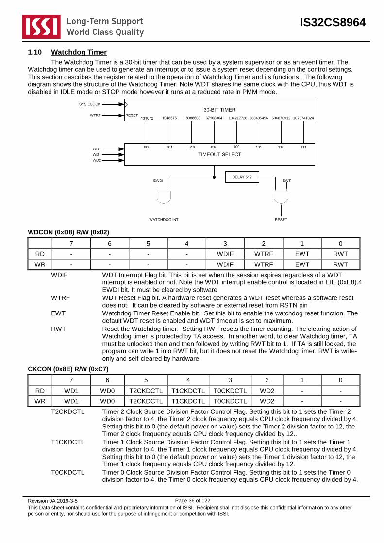
IS32CS8964
Revision 0A 2019-3-5
This Data sheet contains confidential and proprietary information of ISSI. Recipient shall not disclose this confidential information to any other
person or entity, nor should use for the purpose of infringement or competition with ISSI.
Page 36 of 122
1.10 Watchdog Timer
The Watchdog Timer is a 30-bit timer that can be used by a system supervisor or as an event timer. The Watchdog timer can be used to generate an interrupt or to issue a system reset depending on the control settings. This section describes the register related to the operation of Watchdog Timer and its functions. The following diagram shows the structure of the Watchdog Timer. Note WDT shares the same clock with the CPU, thus WDT is disabled in IDLE mode or STOP mode however it runs at a reduced rate in PMM mode.
SYS CLOCK
30-BIT TIMERWTRF RESET
TIMEOUT SELECT
6710886483886081048576131072
WD1
WD2
000 001 010 100
EWDIDELAY 512
EWT
WATCHDOG INT RESET
WD1
010 101 110 111
134217728 268435456 536870912 1073741824
WDCON (0xD8) R/W (0x02)
7 6 5 4 3 2 1 0
RD - - - - WDIF WTRF EWT RWT
WR - - - - WDIF WTRF EWT RWT
WDIF WDT Interrupt Flag bit. This bit is set when the session expires regardless of a WDT interrupt is enabled or not. Note the WDT interrupt enable control is located in EIE (0xE8).4 EWDI bit. It must be cleared by software
WTRF WDT Reset Flag bit. A hardware reset generates a WDT reset whereas a software reset does not. It can be cleared by software or external reset from RSTN pin
EWT Watchdog Timer Reset Enable bit. Set this bit to enable the watchdog reset function. The default WDT reset is enabled and WDT timeout is set to maximum.
RWT Reset the Watchdog timer. Setting RWT resets the timer counting. The clearing action of Watchdog timer is protected by TA access. In another word, to clear Watchdog timer, TA must be unlocked then and then followed by writing RWT bit to 1. If TA is still locked, the program can write 1 into RWT bit, but it does not reset the Watchdog timer. RWT is write-only and self-cleared by hardware.
CKCON (0x8E) R/W (0xC7)
7 6 5 4 3 2 1 0
RD WD1 WD0 T2CKDCTL T1CKDCTL T0CKDCTL WD2 - -
WR WD1 WD0 T2CKDCTL T1CKDCTL T0CKDCTL WD2 - -
T2CKDCTL Timer 2 Clock Source Division Factor Control Flag. Setting this bit to 1 sets the Timer 2 division factor to 4, the Timer 2 clock frequency equals CPU clock frequency divided by 4. Setting this bit to 0 (the default power on value) sets the Timer 2 division factor to 12, the Timer 2 clock frequency equals CPU clock frequency divided by 12..
T1CKDCTL Timer 1 Clock Source Division Factor Control Flag. Setting this bit to 1 sets the Timer 1 division factor to 4, the Timer 1 clock frequency equals CPU clock frequency divided by 4. Setting this bit to 0 (the default power on value) sets the Timer 1 division factor to 12, the Timer 1 clock frequency equals CPU clock frequency divided by 12.
T0CKDCTL Timer 0 Clock Source Division Factor Control Flag. Setting this bit to 1 sets the Timer 0 division factor to 4, the Timer 0 clock frequency equals CPU clock frequency divided by 4.

IS32CS8964
Revision 0A 2019-3-5
This Data sheet contains confidential and proprietary information of ISSI. Recipient shall not disclose this confidential information to any other
person or entity, nor should use for the purpose of infringement or competition with ISSI.
Page 37 of 122
Setting this bit to 0 (the default power on value) sets the Timer 0 division factor equals 12, the Timer 0 clock frequency equals CPU clock frequency divided by 12.
WD[2:0] This register controls the time out value of WDT as the following table. The time out value is shown as follows and the default is set to maximum:
WD2 WD1 WD0 Time Out Value
0 0 0 131072
0 0 1 1048576
0 1 0 8388608
0 1 1 67108864
1 0 0 134217728
1 0 1 268435456
1 1 0 536870912
1 1 1 1073741824
1.11 System Timers – T0 and T1
The CPU contains three 16-bit timers/counters, Timer 0, Timer 1 and Timer 2. In timer mode, Timer 0, Timer 1 registers are incremented every 12 SYSCLK period when the appropriate timer is enabled. In the timer mode, Timer 2 registers are incremented every 12 or 2 SYSCLK period (depending on the operating mode). In the counter mode, the timer registers are incremented every falling edge on their corresponding inputs: T0, T1, and T2. These inputs are read every SYSCLK period.
Timer 0 and Timer 1 are fully compatible with the standard 8051. Timer 0 and 1 are controlled by TCON (0x88) and TMOD (0x89) registers while each timer consists of two 8-bit registers TH0 (0x8C), TL0 (0x8A), TH1 (0x8D), TL1 (0x8B).
TCON (0x88h) Timer 0 and 1 Configuration Register
7 6 5 4 3 2 1 0
RD TF1 TR1 TF0 TR0 PINT1F PINT1EG PINT0F PINT0EG
WR TF1 TR1 TF0 TR0 PINT1F PINT1EG PINT0F PINT0EG
TF1 Timer 1 Interrupt Flag bit. TF1 is cleared by hardware when entering the interrupt routine. TF1 can also be cleared by software.
TR1 Timer 1 Run Control bit. Set to enable Timer 1, and clear to disable Timer 1.
TF0 Timer 0 Interrupt Flag bit. TF0 is cleared by hardware when entering the interrupt routine. TF0 can also be cleared by software.
TR0 Timer 0 Run Control bit. Set to enable Timer 0, and clear to disable Timer 0.
PINT1F/PINT1EG/PINT0F/PINT0EG
These bits are related to configurations of the expanded interrupt PINT1 and PINT0. These are described in the Interrupt System section.
TMOD (0x89h) Timer 0 and 1 Mode Control Register
7 6 5 4 3 2 1 0
RD GATE1 CT1 T1M1 T1M0 GATE0 CT0 T0M1 T0M0
WR GATE1 CT1 T1M1 T1M0 GATE0 CT0 T0M1 T0M0
GATE1 Timer 1 Gate Control bit. Set to enable external T1 to function as gating control of the counter.
CT1 Counter or Timer Mode Select bit. Set CT1 to access external T1 as the clock source. Clear CT1 to use internal clock.
T1M1 Timer 1 Mode Select bit.
T1M0 Timer 1 Mode Select bit.
GATE0 Timer 0 Gate Control bit. Set to enable external T0 to function as gating control of the counter.
CT0 Counter or Timer Mode Select bit. Set CT0 to use external T0 as the clock source. Clear CT0 to use internal clock.
T0M1 Timer 0 Mode Select bit.

IS32CS8964
Revision 0A 2019-3-5
This Data sheet contains confidential and proprietary information of ISSI. Recipient shall not disclose this confidential information to any other
person or entity, nor should use for the purpose of infringement or competition with ISSI.
Page 38 of 122
T0M0 Timer 0 Mode Select bit.
M1 M0 Mode Mode Descriptions
0 0 0 TL serves as a 5-bit pre-scaler and TH functions as an 8-bit counter/timer. They form a 13-bit operation.
0 1 1 TH and TL are cascaded to form a 16-bit counter/timer.
1 0 2 TL functions as an 8-bit counter/timer and auto-reloads from TH.
1 1 3
TL functions as an 8-bit counter/timer. TH functions as an 8-bit timer which is controlled by GATE1. Only Timer 0 can be configured in Mode 3. When this happens, Timer 1 can only be used where its interrupt is not required.
1.11.1 Mode 0
In this mode, TL serves as a 5-bit pre-scaler and TH functions as an 8-bit counter/timer, together working as a 13-bit counter/timer. The Mode 0 operation is shown in the following diagram.
DIV 4
or 12CPUCLK
MUXExternal
T0 or T1
0
1
CT
TR
GATE
TL
5-Bit
TH
8-BitOV INT FLAG
TF0/TF1
CKCON [TxCKDCTL]
1.11.2 Mode 1
Mode 1 operates the same way Mode 0 does, except TL is configured as 8-bit and thus forming a 16-bit counter/timer. This is shown as the following diagram.
DIV 4
or 12CPUCLK
MUXExternal
T0 or T1
0
1
CT
TR
GATE
TL
8-Bit
TH
8-BitOV INT FLAG
TF0/TF1
CKCON [TxCKDCTL]

IS32CS8964
Revision 0A 2019-3-5
This Data sheet contains confidential and proprietary information of ISSI. Recipient shall not disclose this confidential information to any other
person or entity, nor should use for the purpose of infringement or competition with ISSI.
Page 39 of 122
1.11.3 Mode 2
Mode 2 configures the timer as an 8-bit reloadable counter. The counter is TL while TH stores the reload data. The reload occurs when TL overflows. The operation is shown in the following diagram:
DIV 4
or 12CPUCLK
MUX
External
T0 or T1
0
1
CT
TR
GATE
TL
8-Bit
TH
8-Bit
OV INT FLAG
TF0/TF1
RELOAD
CKCON [TxCKDCTL]
1.11.4 Mode 3
Mode 3 is a special mode for Timer 0 only. In this mode, Timer 0 is configured as two separate 8-bit counters. TL0 uses control and interrupt flag of Timer 0, whereas TH0 uses control and interrupt flag of Timer 1. Since Timer 1’s control and flag are occupied, Timer 2 can only be used for counting purposes such as Baud rate generating while Timer 0 is in Mode 3. The operation flow of Mode 3 is shown in the following diagram.
DIV 4
or 12CPUCLK
MUX
T0
0
1
CT0
TR0
GATE0
TL0
8-Bit
TH0
8-Bit
OV INT FLAG
TF0
INT FLAG
TF1OV
TR1CKCON [TxCKDCTL]
1.12 System Timer – T2
Timer 2 is fully compatible with the standard 8052 timer 2. Timer 2 can be used as the reloadable counter, capture timer, or baud rate generator. Timer 2 uses five SFRs as counter registers, capture registers and a control register.
T2CON (0xC8h) Timer 2 Control and Configuration Register
7 6 5 4 3 2 1 0
RD TF2 EXF2 RCLK TCLK EXEN2 TR2 CT2 CPRL2
WR TF2 EXF2 RCLK TCLK EXEN2 TR2 CT2 CPRL2

IS32CS8964
Revision 0A 2019-3-5
This Data sheet contains confidential and proprietary information of ISSI. Recipient shall not disclose this confidential information to any other
person or entity, nor should use for the purpose of infringement or competition with ISSI.
Page 40 of 122
TF2 Timer 2 Interrupt Flag bit.
TF2 must be cleared by software. TF2 is not set when RCLK or TCLK is set (that means Timer 2 is used as a UART0 Baud rate generator).
EXF2 T2EX Falling Edge Flag bit.
This bit is set when T2EX has a falling edge when EXEN2=1. EXF2 must be cleared by software.
RCLK Receive Clock Enable bit
1 – UART0 receiver is clocked by Timer 2 overflow pulses
0 – UART0 receiver is clocked by Timer 1 overflow pulses
TCLK Transmit Clock Enable bit
1 – UART0 transmitter is clocked by Timer 2 overflow pulses
0 – UART0 transmitter is clocked by Timer 1 overflow pulses
EXEN2 T2EX Function Enable bit.
1 – Allows capture or reload as T2EX falling edge appears
0 – Ignore T2EX events
TR2 Start/Stop Timer 2 Control bit
1 – Start
0 – Stop
CT2 Timer 2 Timer/Counter Mode Select bit
1 – External event counter uses T2 pin as the clock source
0 – Internal clock timer mode
CPRL2 Capture/Reload Select bit
1 – Use T2EX pin falling edge for capture
0 – Automatic reload on Timer 2 overflow or falling edge of T2EX (when EXEN2=1). If RCLK or TCLK is set (Timer 2 is used as a baud rate generator), this bit is ignored and an automatic reload is forced on Timer 2 overflows.
Timer 2 can be configured in three modes of operations – Auto-reload Counter, Capture Timer, or Baud Rate Generator. These modes are defined by RCLK, TCLK, CPRL2 and TR2 bits of T2CON registers. The definition is illustrated in the following table:
RCLK or TCLK CPRL2 TR2 Mode Descriptions
0 0 1 16-bit Auto-reload Counter mode. Timer 2 overflow sets the TF2 interrupt flag and TH2/TL2 is reloaded with RLDH/RLHL register.
0 1 1 16-bit Capture Timer mode. Timer 2’s overflow sets TF2 interrupt flag. When EXEN2=1, TH2/TL2 content is captured into RLDH/RLDL when T2EX falling edge occurs.
1 X 1 Baud Rate Generator mode. Timer 2’s overflow is used for configuring UART0.
X X 0 Timer 2 is stopped.
The block diagram of the Timer 2 operating in Auto-reload Counter and Capture Timer modes are shown in the following diagram:
TL2:TH2
16-Bit
RLDL:RLDH
16-Bit
MUX
TR2
CT2
External T2
DIV 12CPUCLK
RELOAD CAPTURE
External T2EXFALLING
DET
EXEN2
T2EXF
T2OV
T2EXF INT FLAG
TF2
CPRL2

IS32CS8964
Revision 0A 2019-3-5
This Data sheet contains confidential and proprietary information of ISSI. Recipient shall not disclose this confidential information to any other
person or entity, nor should use for the purpose of infringement or competition with ISSI.
Page 41 of 122
The block diagram of the Timer 2 operating in Baud Rate Generator is shown in the following diagram:
TL2:TH2
16-Bit
RLDL:RLDH
16-Bit
RELOAD
T2OV MU
XM
UX
MU
X
DIV 2T1OV
DIV 16
DIV 16
RXC
TXC
RCLK
TCLK
PCON.SMOD0
TR2
MU
XDIV 2CPUCLK
External
T2
INT
FLAG
TF2
External
T2EX
FALLING
DET
EXEN2
1.13 System Timer – T3 and T4
Both Timer 3 and Timer 4 are simple 16-Bit reload timers or free-run counters and are clocked by the system clock. The block diagram is shown as below.
T[15-0]
COUNTER[15-0] OV
INTERRUPT
RELOAD
SYSCLK
TR
CPU
TF
TM=1
AUTO RELOAD
TIENTL[15-0]
=
COUNTER[15-0]
OVINTERRUPT
SYSCLK
TR
CPU
TF
TM=0
FREE-RUN
TIEN
T34CON (0xCFh) Timer 3 and Timer 4 Control and Status Register
7 6 5 4 3 2 1 0
RD TF4 TM4 TR4 T4IEN TF3 TM3 TR3 T3IEN
WR TF4 TM4 TR4 T4IEN TF3 TM3 TR3 T3IEN
TF4 Timer 4 Overflow Interrupt Flag bit.
TF4 is set by hardware when overflow condition occurs. TF4 must be cleared by software.
TM4 Timer 4 Mode Control bit. TM4 = 1 set timer 4 as auto reload, and TM4=0 set timer 4 as free-run.
TR4 Timer 4 Run Control bit. Set to enable Timer 4, and clear to stop Timer 4.
T4IEN Timer 4 Interrupt Enable bit.
T4IEN=0 disable the Timer 4 overflow interrupt
T4IEN=1 enable the Timer 4 overflow interrupt
TF3 Timer 3 Overflow Interrupt Flag bit.
TF3 is set by hardware when overflow condition occurs. TF3 must be cleared by software.
TM3 Timer 3 Mode Control bit. TM3 = 1 set timer 3 as auto reload, and TM3=0 set timer 3 as free-run.
TR3 Timer 3 Run Control bit. Set to enable Timer 3, and clear to stop Timer 3.
T3IEN Timer 3 Interrupt Enable bit.
T3IEN=0 disable the Timer 3 overflow interrupt
T3IEN=1 enable the Timer 3 overflow interrupt

IS32CS8964
Revision 0A 2019-3-5
This Data sheet contains confidential and proprietary information of ISSI. Recipient shall not disclose this confidential information to any other
person or entity, nor should use for the purpose of infringement or competition with ISSI.
Page 42 of 122
TL3 (0xAEh) Timer 3 Low Byte Register 0 R/W 00000000
7 6 5 4 3 2 1 0
RD T3[7-0]
WR T3[7-0]
TH3 (0xAFh) Timer 3 High Byte Register 0 R/W 00000000
7 6 5 4 3 2 1 0
RD T3[15-8]
WR T3[15-8]
TL4 (0xACh) Timer 4 Low Byte Register 0 R/W 00000000
7 6 5 4 3 2 1 0
RD T4[7-0]
WR T4[7-0]
TH4 (0xADh) Timer 4 High Byte Register 0 R/W 00000000
7 6 5 4 3 2 1 0
RD T4[15-8]
WR T4[15-8]
T3[15-0] and T4[15-0] function differently when been read or written. When written in auto-reload mode, its reload value register is written, and in free-run mode, the counter value is written immediately. When been read, the return value is always the present counter value. There is no snap-shot buffer in the read operation, so software should always read the high byte then the low byte.
1.14 System Timer – T5
T5 is a 24-Bit simple timer. It can select four different clock sources and can be used for extended sleep mode wake up. The clock sources include IOSC, XOSC, RTC and SIOSC. T5 can be configured either as free-run mode or auto-reload mode. Timer 5 does not depend on the SYSCLK, therefore it continues to count under STOP or SLEEP mode if the clock source is present. The following diagram shows the block diagram of Timer 5.
T5[23-0]
COUNTER[23-0] OV
INTERRUPT
RELOAD
T5CLK
TR
CPU
TF
TM=1
AUTO RELOAD
TIENT5[23-0]
=
COUNTER[23-0]
OV
INTERRUPT
T5CLK
TR
CPU
TF
TM=0
FREE-RUN
TIEN
T5CLK
MUX
T5SEL[1-0]
IOSC
XOSC
RTC
SOSC
00
01
11
10T5CLK
T5CON (0xA003h) Timer 5 Control and Status Register
7 6 5 4 3 2 1 0
RD TF5 T5SEL[1] T5SEL[0] TM5 TR5 - - T5IEN
WR TF5 T5SEL[1] T5SEL[0] TM5 TR5 - - T5IEN
TF5 Timer 5 Overflow Interrupt Flag bit.
TF5 is set by hardware when overflow condition occurs. TF5 must be cleared by software.
T5SEL[1-0] Timer 5 Clock Selection bits.
T5SEL[1-0] = 00, IOSC
T5SEL[1-0] = 01, XOSC
T5SEL[1-0] = 10, RTC
T5SEL[1-0] = 11, SIOSC

IS32CS8964
Revision 0A 2019-3-5
This Data sheet contains confidential and proprietary information of ISSI. Recipient shall not disclose this confidential information to any other
person or entity, nor should use for the purpose of infringement or competition with ISSI.
Page 43 of 122
TM5 Timer 5 Mode Control bit. TM5=1 set timer 5 as auto reload, and TM5=0 set timer 5 as free-run.
TR5 Timer 5 Run Control bit. Set to enable Timer 5, and clear to stop Timer 5.
T5IEN Timer 5 Interrupt Enable bit.
T5IEN=0 disable the Timer 5 overflow interrupt
T5IEN=1 enable the Timer 5 overflow interrupt
TL5 (0xA004) Timer 5 Low Byte Register 0 R/W 00000000
7 6 5 4 3 2 1 0
RD T5[7-0]
WR T5[7-0]
TH5 (0xA005) Timer 5 Medium Byte Register 0 R/W 00000000
7 6 5 4 3 2 1 0
RD T5[15-8]
WR T5[15-8]]
TT5 (0xA006) Timer 5 High Byte Register 0 R/W 00000000
7 6 5 4 3 2 1 0
RD T5[23-16]
WR T5[23-16]
T5[23-0] functions differently when been read or written. When written in auto-reload mode, its reload value register is written, and in free-run mode, the counter value is written immediately. When been read, the return value is always the present counter value. There is no snapshot buffer in the read operation, so software should always read the high byte then the low byte.
1.15 Multiplication and Division Unit (MDU)
MDU provides acceleration on unsigned integer operations of 16-bit multiplications, 32-bit division, and shifting and normalizing operations. The following table shows the execution characteristics of these operations. The MDU does not contain the operation completion status flag. Therefore the most efficient utilization of MDU uses NOP delay for the required clock time of the MDU operation types. The number of the clock cycles required for each operation is shown in the following table and it is counted from the last write of the writing sequence.
Operations Result Reminder # of Clock Cycle
32-bit division by 16-bit 32-bit 16-bit 17
16-bit division by 16-bit 16-bit 16-bit 9
16-bit multiplication by 16-bit 32-bit - 10
32-bit normalization - - 3 – 20
32-bit shift left/right - - 3 – 18
The MDU is accessed through MD0 to MD5 that contains the operands and the results, and the operation is controlled by ARCON register.
ARCON (0xFF) MDU Control R/W 00000000
7 6 5 4 3 2 1 0
RD MDEF MDOV SLR SC4 SC3 SC2 SC1 SC0
WR MDEF MDOV SLR SC4 SC3 SC2 SC1 SC0
MDEF MDU Error Flag bit. Set by hardware to indicate MDx being written before the previous operation completes. MDEF is automatically cleared after reading ARCON.
MDOV MDU Overflow Flag bit. MDOV is set by hardware if dividend is zero or the result of multiplication is greater than 0x0000FFFFh
SLR Shift Direction Control bit. SLR = 1 indicates a shift to the right and SLR =0 indicates a shift to the left.

IS32CS8964
Revision 0A 2019-3-5
This Data sheet contains confidential and proprietary information of ISSI. Recipient shall not disclose this confidential information to any other
person or entity, nor should use for the purpose of infringement or competition with ISSI.
Page 44 of 122
SC4-0 Shift Count Control and Result bit. If SC0-4 is written with 00000, the normalization operation performed by MDU. When the normalization is completed, SC4-0 contains the number of shift performed in the normalization. If SC4-0 is written with a non-zero value, then the shift operation is performed by MDU with the number of shift specified by SC4-0 value.
MD0 (0xF9) MDU Data Register 0 R/W 00000000
7 6 5 4 3 2 1 0
RD MD0[7-0]
WR MD0[7-0]
MD1 (0xFA) MDU Data Register 1 R/W 00000000
7 6 5 4 3 2 1 0
RD MD1[7-0]
WR MD1[7-0]
MD2 (0xFB) MDU Data Register 2 R/W 00000000
7 6 5 4 3 2 1 0
RD MD2[7-0]
WR MD2[7-0]
MD3 (0xFC) MDU Data Register 3 R/W 00000000
7 6 5 4 3 2 1 0
RD MD3[7-0]
WR MD3[7-0]
MD4 (0xFD) MDU Data Register 4 R/W 00000000
7 6 5 4 3 2 1 0
RD MD4[7-0]
WR MD4[7-0]
MD5 (0xFE) MDU Data Register 5 R/W 00000000
7 6 5 4 3 2 1 0
RD MD5[7-0]
WR MD5[7-0]
MDU operation consists of three phases.
Loading MD0 to MD5 data registers in an appropriate order depending on the operation.
Execution of the operation.
Reading result from MD0 to MD5 registers.
The following list shows the MDU read and write sequences. Each operation has its unique writing sequence and reading sequence of MD0 to MD5 registers therefore a precise access sequence is required.
1.15.1 Division – 32-bit divide by 16-bit or 16-bit divide by 16-bit
Follow the following write-sequence. The first write of MD0 resets the MDU and initiates the MDU error flag mechanism. The last write incites calculation of MDU.
Write MD0 with Dividend LSB byte
Write MD1 with Dividend LSB+1 byte
Write MD2 with Dividend LSB+2 byte (ignore this step for 16-bit divide by 16-bit)
Write MD3 with Dividend MSB byte (ignore this step for 16-bit divide by 16-bit)
Write MD4 with Divisor LSB byte
Write MD5 with Divisor MSB byte

IS32CS8964
Revision 0A 2019-3-5
This Data sheet contains confidential and proprietary information of ISSI. Recipient shall not disclose this confidential information to any other
person or entity, nor should use for the purpose of infringement or competition with ISSI.
Page 45 of 122
Then follow the following read-sequence. The last read prompts MDU for the next operations.
Read MD0 with Quotient LSB byte
Read MD1 with Quotient LSB+1 byte
Read MD2 with Quotient LSB+2 byte (ignore this step for 16-bit divide by 16-bit)
Read MD3 with Quotient MSB byte (ignore this step for 16-bit divide by 16-bit)
Read MD4 with Remainder LSB byte
Read MD5 with Remainder MSB byte
Read ARCON to determine error or overflow condition
Please note if the sequence is violated, the calculation may be interrupted and result in errors.
1.15.2 Multiplication – 16-bit multiply by 16-bit
Follow the following write sequence.
Write MD0 with Multiplicand LSB byte
Write MD4 with Multiplier LSB byte
Write MD1 with Multiplicand MSB byte
Write MD5 with Multiplier MSB byte
Then follow the following read sequence.
Read MD0 with Product LSB byte
Read MD1 with Product LSB+1 byte
Read MD2 with Product LSB+2 byte
Read MD3 with Product MSB byte
Read ARCON to determine error or overflow condition
1.15.3 Normalization – 32-bit
Normalization is obtained with integer variables stored in MD0 to MD3. After normalization, all leading zeroes are removed by shift left operations. To start the normalization operation, SC4-0 in ARCON is first written with 00000. After completion of the normalization, SC4-0 is updated with the number of leading zeroes and the normalized result is restored on MD0 to MD3. The number of the shift of the normalization can be used as exponents. The following write sequence should be followed. The last write to ARCON initiates the normalization operations by MDU.
Write MD0 with Operand LSB byte
Write MD1 with Operand LSB+1 byte
Write MD2 with Operand LSB+2 byte
Write MD3 with Operand MSB byte
Write ARCON with SC4-0 = 00000
Then follow the following read sequence.
Read MD0 with Result LSB byte
Read MD1 with Result LSB+1 byte
Read MD2 with Result LSB+2 byte
Read MD3 with Result MSB byte
Read SC[4-0] from ARCON for normalization count or error flag
1.15.4 Shift – 32-bit
Shift is done with integer variables stored in MD0 to MD3. To start the shift operation, SC4-0 in ARCON is first written with shift count and SLR with shift direction. After completion of the Shift, the result is stored back to MD0 to MD3. The following write sequence should be followed. The last write to ARCON initiates the normalization operations by MDU.
Write MD0 with Operand LSB byte
Write MD1 with Operand LSB+1 byte
Write MD2 with Operand LSB+2 byte
Write MD3 with Operand MSB byte
Write ARCON with SC4-0 = Shift count and SLR with shift direction
IS32CS8964
Revision 0A 2019-3-5
This Data sheet contains confidential and proprietary information of ISSI. Recipient shall not disclose this confidential information to any other
person or entity, nor should use for the purpose of infringement or competition with ISSI.
Page 46 of 122
Then follow the following read sequence.
Read MD0 with Result LSB byte
Read MD1 with Result LSB+1 byte
Read MD2 with Result LSB+2 byte
Read MD3 with Result MSB byte
Read ARCON’s for error flag
1.15.5 MDU Flag
The error flag (MDEF) of MDU indicates improperly performed operations. The error mechanism starts at the first MD0 write and finishes with the last read of MD result register. MDEF is set if current operation is interrupted or restarted by improper write of MD register before the operation completes. MDEF is cleared if the operations and proper write/read sequences successfully complete. The overflow flag (MDOV) of MDU indicates an error of operations. MDOV is set if
the divisor is zero
Multiplication overflows
Normalization operation is performed on already normalized variables (MD3.7 =1)
1.16 Serial Port – UART0
UART0 is full duplex and fully compatible with the standard 8052 UART. The receive path of the UART0 is double-buffered that can commence reception of second byte before previously received byte is read from the receive register. Writing to SBUF0 loads the transmit register while reading SBUF0, reads a physically separate receive register. The UART0 can operate in four modes: one synchronous (Mode 0) and three asynchronous modes (Mode 1, 2, and 3). Mode 2 and Mode 3 share a special provision for multi-processor communications. This feature is enabled by setting SM2 bit in SCON0 register. The master processor first sends out an address byte which identifies the slave. An address byte differs from a data byte in the 9
th bit: 1 defines an address byte whereas 0 defines a data byte. When
SM2 is set to 1, no slave can be interrupted by a data byte. An address byte can interrupt slaves. The addressed slave clears its SM2 bit and prepares to receive the following incoming data bytes. The slaves that are not addressed leave their SM2 set and ignore the incoming data. The UART0-related registers are SBUF0, SCON0, PCON, IE, and IP.
SCON0 (0x98h) UART0 Configuration Register
7 6 5 4 3 2 1 0
RD SM0 SM1 SM2 REN TB8 RB8 TIF RIF
WR SM0 SM1 SM2 REN TB8 RB8 TIF RIF
SM0, SM1 UART Operation Mode
MODE SM0 SM1 Description
0 0 0 Synchronous Shift Register Mode
Baud rate = CPUCLK/12
1 0 1 8-Bit UART Mode
Baud rate = Timer 1 or Timer 2 overflow rate. This is selected in T2CON registers.
2 1 0 9-Bit UART Mode, fix baud rate
Baud rate = CPUCLK/64 (PCON.SMOD0 = 0) or CPUCLK/32 (PCON.SMOD0 = 1)
3 1 1 9-Bit UART Mode, variable baud rate
Baud rate = Timer 1 or Timer 2 overflow rate. This is selected in TCON registers.
SM2 Set to enable a multiprocessor communication as a slave device.
REN Set REN=1 to enable UART PMM switch back function. REN=0 disables this function. In PMM mode, if REN=1, then any transition on RX of UART triggers the exit of PMM mode into normal mode.
TB8 The transmit-value of 9th bit in 9-bit UART mode (mode 2 and mode 3). Set or cleared by
CPU depending on the function of the 9th bit as a parity check bit or a multi-processor.
RB8 The receive-value of 9th bit in 9-bit UART mode (mode 2 and mode 3). Set or cleared by
hardware.

IS32CS8964
Revision 0A 2019-3-5
This Data sheet contains confidential and proprietary information of ISSI. Recipient shall not disclose this confidential information to any other
person or entity, nor should use for the purpose of infringement or competition with ISSI.
Page 47 of 122
TIF Transmit Interrupt Flag bit. Set by hardware after completion of a serial transmission and must be cleared by software. The interrupt enable bit is located in IE (0xA8) and the interrupt priority is located in IP (0xB8).
RIF Receive Interrupt Flag bit. Set by hardware after completion of a serial reception and must be cleared by software. The interrupt enable bit is located in IE (0xA8) and the interrupt priority is located in IP (0xB8).
SBUF0 (0x99h) UART0 Data Buffer Register
7 6 5 4 3 2 1 0
RD RB[7-0]
WR TB[7-0]
SBUF0 is used for both transmission and reception. Writing a data byte into SBUF0 puts this data in UART0’s transmit buffer and starts a transmission. Reading a byte from SBUF means data being read from the UART0’s receive buffer.
1.16.1 Mode 0
Mode 0 is a simple synchronous shift register mode. TXD0 outputs the shift clock which is fixed at CPUCLK/12. RXD0 is a bidirectional I/O port that serves as a data-shifting port. To utilize this mode, TXD0 pin must be enabled as an output pin, while RXD0 needs to be configured as an open-drain type of I/O port. The shift data changes at the rising edge of the shift clock and is valid at the falling edge of the shift clock. The transmission starts when a new byte is written in SBUF0 as TI is cleared to 0. When the byte is transmitted, TI is set and the UART0 waits for the next byte to be transmitted. The reception is initiated by setting REN=1 and RI cleared to 0. When a byte is received, RI is set by UART0.
1.16.2 Mode 1
8-bit UART mode. RXD0 is the serial input and TXD0 is the serial output. To utilize this mode, the corresponding RXD0 and TXD0 pin configuration should also be set correctly. 10-bit data (including a Start bit, 8 data bit, and a Stop bit) are transferred. For UART0, the baud rate is set by Timer 1 or Timer 2 overflow rate. The control is determined by SMOD0.PCON, and RCLK.T2CON, TCLK.T2CON. When SMOD0.PCON is 1, Timer 1 overflow is selected, and SMOD0.PCON is 0, Timer 1 overflow rate divided by 2 is selected. And if RCLK.T2CON, or TCLK.T2CON is set, the Timer 2 overflow rate is selected and overwrites the SMOD0 setting.
1.16.3 Mode 2
9-bit UART mode. RXD0 is the serial input and TXD0 is the serial output. To utilize this mode, the corresponding RXD0 and TXD0 pins should be configured correctly. 11-bit data including a Start bit (always 0), 8 data bits, a programmable 9
th bit, and a Stop bit (always 1) are transferred. The 9
th bit can be configured as a parity bit
configured by software through TB8 in SCON0. The received 9th bit can be read from TB8. The software determines
the correctness of the parity check. The baud rate in Mode 2 is fixed at 1/32 or 1/64 of CPU clock. This is controlled by SMOD0 in PCON register.
1.16.4 Mode 3
Similar to Mode 2 (9-bit UART mode). RXD0 is the serial input and TXD0 is the serial output. To utilize this mode, the corresponding RXD0 and TXD0 pins should also be configured properly. 11-bit data including a Start bit (always 0), 8 data bits, a programmable 9
th bit, and a Stop bit (always 1) are transferred. The 9
th bit can serve as a
parity bit configured by software through TB8 in SCON0. The received 9th bit can be read from TB8. The software
determines the correctness of the parity check. The mechanism of the baud rate control in Mode 3 is similar to which in Mode 1 that is determined by Timer 1 or Timer 2 overflow and is set by SMOD0, and T2CON.
1.17 I2C Master
The I2C master controller provides the interface to I
2C slave devices. It can be programmed to operate with
arbitration and clock synchronization to allow it to operate in multi-master configurations. The master uses SCL and SDA pins. The controller contains a built-in 8-bit timer to allow various I
2C bus speed.
I2CMTP (0xF7h) I2C Master Time Period R/W 00000000
7 6 5 4 3 2 1 0
RD I2CMTP[7-0]
WR I2CMTP[7-0]
This register set the period time of I2C bus clock – SCL. The SCL period time is set according to
SCLPERIOD = 8 * (1 + I2CMTP) * CPUCLK_PERIORD when the I2CMTP[7-0] is equal to or larger than 0x01. If

IS32CS8964
Revision 0A 2019-3-5
This Data sheet contains confidential and proprietary information of ISSI. Recipient shall not disclose this confidential information to any other
person or entity, nor should use for the purpose of infringement or competition with ISSI.
Page 48 of 122
I2CMTP[7-0] = 0x00, the maximum I2C bus speed is limited to SYSCLK/12.
I2CMSA (0xF4) I2C Master Slave Address R/W 00000000
7 6 5 4 3 2 1 0
RD SA[6-0] RS
WR SA[6-0] RS
SA[6-0] Slave Address. SA[6-0] defines the slave address the I2C master uses to communicate.
RS Receive/Send Bit. RS determines if the following operation is to RECEIVE (RS=1) or SEND (RS=0).
I2CMBUF (0xF6) I2C Master Data Buffer Register R/W 00000000
7 6 5 4 3 2 1 0
RD RD[7-0]
WR TD[7-0]
I2CMBUF functions as a transmit-data register when written and as a receive-data register when read. When written, TD is sent to the bus by the next SEND or BURST SEND operations. TD[7] is sent first. When read, RD contains the 8-bit data received from the bus upon the last RECEIVE or BURST RECEIVE operation.
I2CMCR (0xF5) I2C Master Control and Status Register R/W 00000000
7 6 5 4 3 2 1 0
RD - BUSBUSY IDLE ARBLOST DATAACK ADDRACK ERROR BUSY
WR I2CMRST INFILEN - HS ACK STOP START RUN
The I2CMCR register is used for setting control when it is written, and as a status signal when read.
I2CMRST Writing 1 to this bit forces the I2CM to perform reset and clear its internal state machine. At the end of the initialization, all SFRs will return to the default value. This bit is cleared automatically by hardware.
INFILEN Input Noise Filter Enable. When IFILEN is set, pulses shorter than 50 nsec on inputs of SDA and SCL are filtered out.
IDLE This bit indicates that I2C master is in the IDLE mode.
BUSY This bit indicates that I2C master is receiving or transmitting data, and other status bits are
not valid.
BUSBUSY This bit indicates that the external I2C bus is busy and access to the bus is not possible.
This bit is set/reset by START and STOP conditions.
ERROR This bit indicates that an error occurs in the last operation. The errors include slave address was not acknowledged, or transmitted data is not acknowledged, or the master controller loses arbitration.
ADDRERR This bit is automatically set when the last operation slave address transmitted is not acknowledged.
DATAERR This bit is automatically set when the last operation transmitted data is not acknowledged.
ARBLOST This bit is automatically set when the last operation I2C master controller loses the bus
arbitration.
START, STOP, RUN and HS, RS, ACK bits are used to drive I2C Master to initiate and terminate a transaction. The
Start bit generates START, or REPEAT START protocol. The Stop bit determines if the cycle stops at the end of the data cycle or continues to a burst. To generate a single read cycle, the designated address is written in SA, RS is set to 1, ACK=0, STOP=1, START=1, RUN=1 are set in I2CMCR to perform the operation and then STOP. When the operation is completed (or aborted due to errors), I
2C master generates an interrupt. The ACK bit must be set to 1.
This causes the controller to send an ACK automatically after each byte transaction. The ACK bit must be reset when set to 0 when the master operates in receive mode and not to receive further data from the slave devices.
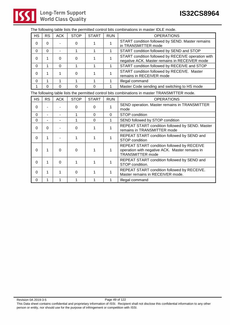
IS32CS8964
Revision 0A 2019-3-5
This Data sheet contains confidential and proprietary information of ISSI. Recipient shall not disclose this confidential information to any other
person or entity, nor should use for the purpose of infringement or competition with ISSI.
Page 49 of 122
The following table lists the permitted control bits combinations in master IDLE mode.
HS RS ACK STOP START RUN OPERATIONS
0 0 - 0 1 1 START condition followed by SEND. Master remains in TRANSMITTER mode
0 0 - 1 1 1 START condition followed by SEND and STOP
0 1 0 0 1 1 START condition followed by RECEIVE operation with negative ACK. Master remains in RECEIVER mode
0 1 0 1 1 1 START condition followed by RECEIVE and STOP
0 1 1 0 1 1 START condition followed by RECEIVE. Master remains in RECEIVER mode
0 1 1 1 1 1 Illegal command
1 0 0 0 0 1 Master Code sending and switching to HS mode
The following table lists the permitted control bits combinations in master TRANSMITTER mode.
HS RS ACK STOP START RUN OPERATIONS
0 - - 0 0 1 SEND operation. Master remains in TRANSMITTER mode
0 - - 1 0 0 STOP condition
0 - - 1 0 1 SEND followed by STOP condition
0 0 - 0 1 1 REPEAT START condition followed by SEND. Master remains in TRANSMITTER mode
0 1 - 1 1 1 REPEAT START condition followed by SEND and STOP condition
0 1 0 0 1 1 REPEAT START condition followed by RECEIVE operation with negative ACK. Master remains in TRANSMITTER mode
0 1 0 1 1 1 REPEAT START condition followed by SEND and STOP condition.
0 1 1 0 1 1 REPEAT START condition followed by RECEIVE. Master remains in RECEIVER mode.
0 1 1 1 1 1 Illegal command

IS32CS8964
Revision 0A 2019-3-5
This Data sheet contains confidential and proprietary information of ISSI. Recipient shall not disclose this confidential information to any other
person or entity, nor should use for the purpose of infringement or competition with ISSI.
Page 50 of 122
The following table lists the permitted control bits combinations in master RECEIVER mode.
HS RS ACK STOP START RUN OPERATIONS
0 - 0 0 0 1 RECEIVE operation with negative ACK. Master remains in RECEIVE mode
0 - - 1 0 0 STOP condition
0 - 0 1 0 1 RECEIVE followed by STOP condition
0 - 1 0 0 1 RECEIVE operation. Master remains in RECEIVER mode
0 - 1 1 0 1 Illegal command
0 1 0 0 1 1 REPEAT START condition followed by RECEIVE operation with negative ACK. Master remains in RECEIVER mode
0 1 0 1 1 1 REPEAT START condition followed by RECEIVE and STOP conditions
0 1 0 1 1 1 REPEAT START condition followed by RECEIVE. Master remains in RECEIVER mode
0 0 - 0 1 1 REPEAT START condition followed by SEND. Master remains in TRANSMITTER mode.
0 0 - 1 1 1 REPEAT START condition followed by SEND and STOP conditions.
All other control-bit combinations not included in three tables above are NOP. In Master RECEIVER mode, STOP should be generated only after data negative ACK executed by Master or address negative ACK executed by slave. Negative ACK means SDA is pulled low when the acknowledge clock pulse is generated.
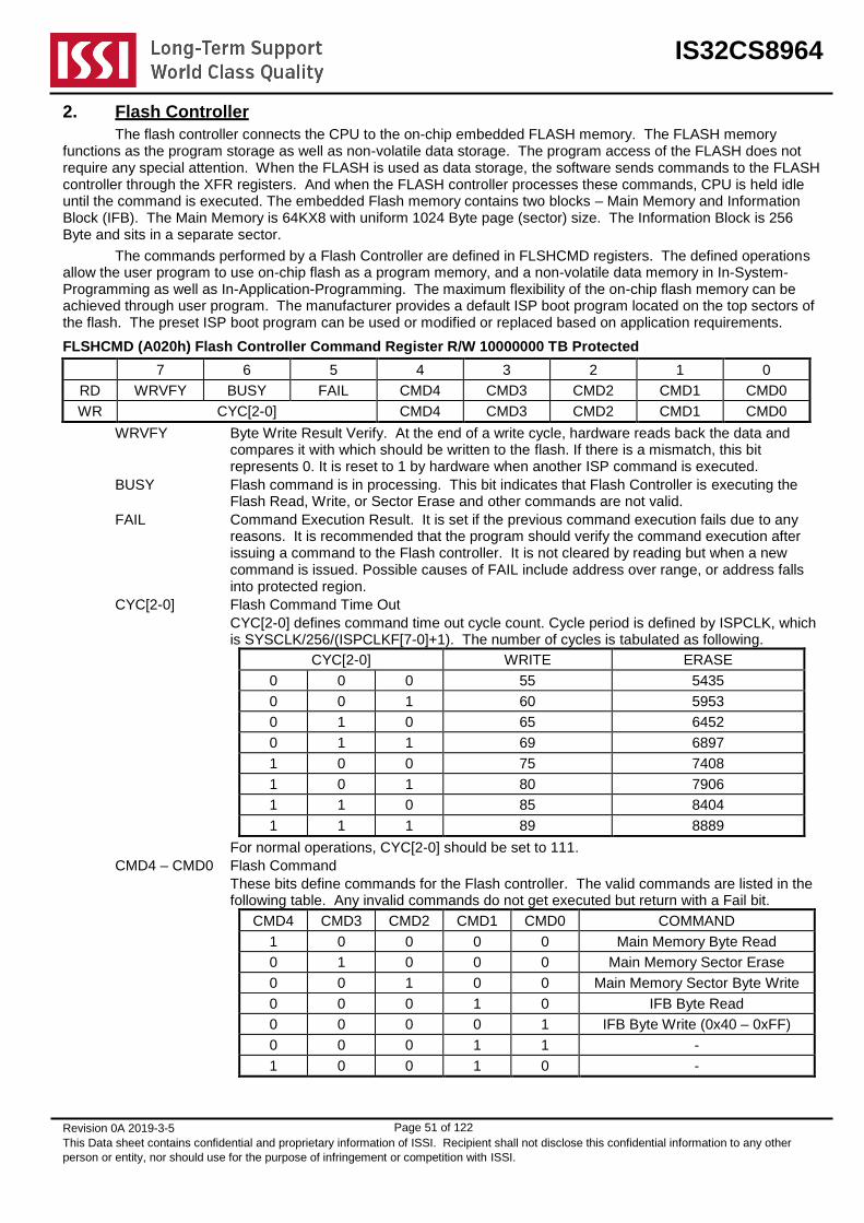
IS32CS8964
Revision 0A 2019-3-5
This Data sheet contains confidential and proprietary information of ISSI. Recipient shall not disclose this confidential information to any other
person or entity, nor should use for the purpose of infringement or competition with ISSI.
Page 51 of 122
2. Flash Controller
The flash controller connects the CPU to the on-chip embedded FLASH memory. The FLASH memory functions as the program storage as well as non-volatile data storage. The program access of the FLASH does not require any special attention. When the FLASH is used as data storage, the software sends commands to the FLASH controller through the XFR registers. And when the FLASH controller processes these commands, CPU is held idle until the command is executed. The embedded Flash memory contains two blocks – Main Memory and Information Block (IFB). The Main Memory is 64KX8 with uniform 1024 Byte page (sector) size. The Information Block is 256 Byte and sits in a separate sector.
The commands performed by a Flash Controller are defined in FLSHCMD registers. The defined operations allow the user program to use on-chip flash as a program memory, and a non-volatile data memory in In-System-Programming as well as In-Application-Programming. The maximum flexibility of the on-chip flash memory can be achieved through user program. The manufacturer provides a default ISP boot program located on the top sectors of the flash. The preset ISP boot program can be used or modified or replaced based on application requirements.
FLSHCMD (A020h) Flash Controller Command Register R/W 10000000 TB Protected
7 6 5 4 3 2 1 0
RD WRVFY BUSY FAIL CMD4 CMD3 CMD2 CMD1 CMD0
WR CYC[2-0] CMD4 CMD3 CMD2 CMD1 CMD0
WRVFY Byte Write Result Verify. At the end of a write cycle, hardware reads back the data and compares it with which should be written to the flash. If there is a mismatch, this bit represents 0. It is reset to 1 by hardware when another ISP command is executed.
BUSY Flash command is in processing. This bit indicates that Flash Controller is executing the Flash Read, Write, or Sector Erase and other commands are not valid.
FAIL Command Execution Result. It is set if the previous command execution fails due to any reasons. It is recommended that the program should verify the command execution after issuing a command to the Flash controller. It is not cleared by reading but when a new command is issued. Possible causes of FAIL include address over range, or address falls into protected region.
CYC[2-0] Flash Command Time Out
CYC[2-0] defines command time out cycle count. Cycle period is defined by ISPCLK, which is SYSCLK/256/(ISPCLKF[7-0]+1). The number of cycles is tabulated as following.
CYC[2-0] WRITE ERASE
0 0 0 55 5435
0 0 1 60 5953
0 1 0 65 6452
0 1 1 69 6897
1 0 0 75 7408
1 0 1 80 7906
1 1 0 85 8404
1 1 1 89 8889
For normal operations, CYC[2-0] should be set to 111.
CMD4 – CMD0 Flash Command
These bits define commands for the Flash controller. The valid commands are listed in the following table. Any invalid commands do not get executed but return with a Fail bit.
CMD4 CMD3 CMD2 CMD1 CMD0 COMMAND
1 0 0 0 0 Main Memory Byte Read
0 1 0 0 0 Main Memory Sector Erase
0 0 1 0 0 Main Memory Sector Byte Write
0 0 0 1 0 IFB Byte Read
0 0 0 0 1 IFB Byte Write (0x40 – 0xFF)
0 0 0 1 1 -
1 0 0 1 0 -
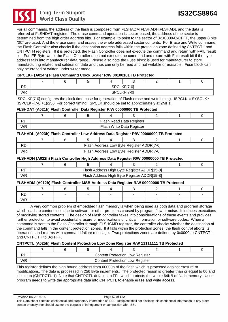
IS32CS8964
Revision 0A 2019-3-5
This Data sheet contains confidential and proprietary information of ISSI. Recipient shall not disclose this confidential information to any other
person or entity, nor should use for the purpose of infringement or competition with ISSI.
Page 52 of 122
For all commands, the address of the flash is composed from FLSHADM:FLSHADH:FLSHADL and the data is referred at FLSHDAT registers. The erase command operation is sector-based, the address of the sector is determined from the high order address bits. For example, to point to the sector of 0x0C000-0xCFFF, the upper 8 bits “0C” are used. And the erase command erases the whole addressed sector contents. For Erase and Write command, the Flash Controller also checks if the destination address falls within the protection zone defined by CNTPCTL and CNTPCTH registers. If it is protected, the Flash Controller does not execute the command and return with FAIL result bit. For IFB Byte-write, the Flash Controller does not execute the command and return with Fail result bit if the byte address falls into manufacturer data range. Please also note the Fuse block is used for manufacturer to store manufacturing related and calibration data and thus can only be read and not writable or erasable. Fuse block can only be erased or written under writer mode.
ISPCLKF (A024h) Flash Command Clock Scaler R/W 00100101 TB Protected
7 6 5 4 3 2 1 0
RD ISPCLKF[7-0]
WR ISPCLKF[7-0]
ISPCLKF[7-0] configures the clock time base for generation of Flash erase and write timing. ISPCLK = SYSCLK * (ISPCLKF[7-0]+1)/256. For correct timing, ISPCLK should be set to approximately at 2MHz.
FLSHDAT (A021h) Flash Controller Data Register R/W 00000000 TB Protected
7 6 5 4 3 2 1 0
RD Flash Read Data Register
WR Flash Write Data Register
FLSHADL (A023h) Flash Controller Low Address Data Register R/W 00000000 TB Protected
7 6 5 4 3 2 1 0
RD Flash Address Low Byte Register ADDR[7-0]
WR Flash Address Low Byte Register ADDR[7-0]
FLSHADH (A022h) Flash Controller High Address Data Register R/W 00000000 TB Protected
7 6 5 4 3 2 1 0
RD Flash Address High Byte Register ADDR[15-8]
WR Flash Address High Byte Register ADDR[15-8]
FLSHADM (A012h) Flash Controller MSB Address Data Register R/W 00000000 TB Protected
7 6 5 4 3 2 1 0
RD - - - - - - - -
WR - - - - - - - -
A very common problem of embedded flash memory is when being used as both data and program storage which leads to content loss due to software or other problems caused by program flow or noise. It induces executions of modifying stored contents. The design of Flash controller takes into considerations of these events and provides further protection to avoid accidental erasure or modifications of critical information or software codes. When a command is sent to the Flash Controller through FLSHCMD register, the controller checks whether the destination of the command falls in the content protection zones. If it falls within the protection zones, the flash control aborts its operations and returns with command failure message. Two protections zones are defined by 0x0000 to CNTPCTL and CNTPCTH to 0xFFFF.
CNTPCTL (A025h) Flash Content Protection Low Zone Register R/W 11111111 TB Protected
7 6 5 4 3 2 1 0
RD Content Protection Low Register
WR Content Protection Low Register
This register defines the high bound address from 00000h of the flash which is protected against erasure or modifications. The data is processed in 256 Byte increments. The protected region is greater than or equal to 00 and less than (CNTPCTL-1). Note that CNTPCTL defaults to FFh which protects the whole 64KB of flash memory. User program needs to write the appropriate data into CNTPCTL to enable erase and write access.

IS32CS8964
Revision 0A 2019-3-5
This Data sheet contains confidential and proprietary information of ISSI. Recipient shall not disclose this confidential information to any other
person or entity, nor should use for the purpose of infringement or competition with ISSI.
Page 53 of 122
CNTPCTH (A026h) Flash Content Protection High Zone Register R/W 00000000 TB Protected
7 6 5 4 3 2 1 0
RD Content Protection High Register
WR Content Protection High Register
This register defines the low bound address from 0xFFFF of the flash to be protected against erasure or modifications. The data is processed in the increments of 256 Byte. The protected region is greater than (CNTPCTH+1) and less than or equal to FF. Note that CNTPCTH1 defaults to 00h which means the protection of 64KB of flash memory is on. User program needs to write the appropriate data into CNTPCTH1 by reading IFB-protected information to protect boot code and expand the protection zone under application considerations.
There is an additional content protection against internal program. This protects sensitive data from unauthorized access. The protection range is from 0x1000 to 0xFFFF of embedded flash memory. The protection is achieved by two special registers, INTPCT1 (0xA013) and INTPCT2 (0xA014). After any reset condition such as power-up, RSTN, LVR, or WDT reset, INTPCT1 and INTPCT2 are initialized to 0x00. The bits in INTPCT1 and INTPCT2 can only be written to “1”. When the embedded flash memory has been protected, this means accessing this protected range returns with 0x00 either by program instruction such as “MOVC” or by Flash Main Memory Byte Read access. The internal protection is by default not turned on after reset because both INTPCT1 and INTPCT2 are 0x00. Both registers are protected by TB. To turn on the internal protection, INTPCEN must be enabled by writing a “0x80” into enable the Internal Protection function. When INTPCEN is set, user can define the protection range by program INTPCT1 or INTPCT2. The INTPCEN will be cleared and stuck-on zero after setting any protection range. In other words, the protection range is single time programmable. Once the protection is turned on, it can’t be turned off or modified because INTPCEN is stuck-on zero. To restore unprotected state, the chip must go through a reset. The internal protection should be enabled with extreme cautiousness. It is important that once it is turned on, program execution should not reach the protected zone, otherwise unpredicted program errors may occur.
INTPCT1 (A013h) Internal Protection Enable Register R/W 00000000 TB Protected
7 6 5 4 3 2 1 0
RD INTPCT1[7-0]
WR INTPCT1[7-0]
This register can be written to “1” only. Writing “0” into any bit of this register does not alter the content. This register is cleared to 0x00 after reset. And the value of this register can be cleared only by a reset.
INTPCT2 (A014h) Internal Protection Enable Register R/W 00000000 TB Protected
7 6 5 4 3 2 1 0
RD INTPCEN INTPCT2[6-0]
WR INTPCEN INTPCT2[6-0]
This register can be written to “1” only. Writing “0” into any bit of this register does not alter the content. This register is set to 0x00 after a reset. And the value of this register can be set only by a reset.
INTPCEN INTPCT1/INTPCT2 updates enable. This bit is single time programmable. After setting any protection range, this bit will be stuck-on zero and prohibit another protection updating. Because the INTPCEN is disabled in the initiation, a “0x80” must be programmed into INTPCT2 to enable INTPCEN. When INTPCEN is set, the expected program protection can be defined by setting INTPC1 or INTPC2[6-0].
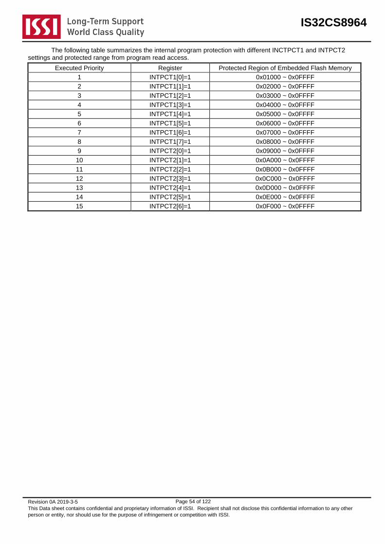
IS32CS8964
Revision 0A 2019-3-5
This Data sheet contains confidential and proprietary information of ISSI. Recipient shall not disclose this confidential information to any other
person or entity, nor should use for the purpose of infringement or competition with ISSI.
Page 54 of 122
The following table summarizes the internal program protection with different INCTPCT1 and INTPCT2 settings and protected range from program read access.
Executed Priority Register Protected Region of Embedded Flash Memory
1 INTPCT1[0]=1 0x01000 ~ 0x0FFFF
2 INTPCT1[1]=1 0x02000 ~ 0x0FFFF
3 INTPCT1[2]=1 0x03000 ~ 0x0FFFF
4 INTPCT1[3]=1 0x04000 ~ 0x0FFFF
5 INTPCT1[4]=1 0x05000 ~ 0x0FFFF
6 INTPCT1[5]=1 0x06000 ~ 0x0FFFF
7 INTPCT1[6]=1 0x07000 ~ 0x0FFFF
8 INTPCT1[7]=1 0x08000 ~ 0x0FFFF
9 INTPCT2[0]=1 0x09000 ~ 0x0FFFF
10 INTPCT2[1]=1 0x0A000 ~ 0x0FFFF
11 INTPCT2[2]=1 0x0B000 ~ 0x0FFFF
12 INTPCT2[3]=1 0x0C000 ~ 0x0FFFF
13 INTPCT2[4]=1 0x0D000 ~ 0x0FFFF
14 INTPCT2[5]=1 0x0E000 ~ 0x0FFFF
15 INTPCT2[6]=1 0x0F000 ~ 0x0FFFF

IS32CS8964
Revision 0A 2019-3-5
This Data sheet contains confidential and proprietary information of ISSI. Recipient shall not disclose this confidential information to any other
person or entity, nor should use for the purpose of infringement or competition with ISSI.
Page 55 of 122
3. I2C Slave Controller 1 (I2CS1)
The I2C Slave Controller 1 is a regular I
2C Slave controller with enhanced functions such as clock-stretching
and programmable hold time. These enhancements provide significant improvement on compatibilities. I2CS1 shares the SCL/SDA pins with the I2CM1. I2CS1 also can be configured to respond to two I
2C addresses – I2CADR1
and I2CADR3. These two addresses can be enabled separately.
In receive mode, the controller detects a valid matching address and issues an ADDRMI interrupt. At the same time, the data bit on SDA line is shifted into receive buffer. The RCBI interrupt is generated whenever a complete byte is received and is ready to be read from I2CSDAT. If for any reason, the software does not respond to RCBI interrupt in time (i.e. RCBI is not cleared), and a new byte is received, the controller either forces an NACK response on I
2C (if CLKSTREN bit is not set) or by pulling and holding SDA low (if CLKSTREN bit is set) to stretch the
SCL low duration to force the master into a wait state. In clock stretching mode, SCL is released when the software responds to RCBI interrupt and cleared RCBI flag.
In transmit mode, the controller detects a valid matching address and issue an ADDRMI interrupt. At the same time, the data preloaded in the transmit data register through I2CSDAT is transferred to the transmit shift register and is serially shifted out onto SDA line. When this occurs, the controller generates a TXBI interrupt to inform the software that a new byte can be written into I2CSDAT. When the shift register is empty and ready for the next transmit, the slave controller checks if the new byte is written to the I2CSDAT. If TXBI is not cleared, it indicates lack of new data and the slave controller holds SCL line low to stretch the current clock cycle if CLKSTREN is set. If the clock stretching is not enabled, the slave controller takes the old byte into the shift register and replies with NACK, thus causing data corruption. On the other hand, if the master returns the NACK after the byte transfer, this indicates the end of data to the I
2C slave. In this case, the I
2C slave releases the data line to allow the master to generate a STOP
or REPEAT START.
The I2C slave controller also implements the input noise spike filter. This is enabled by the INFILEN bit in the
I2CSCON register. The filter is implemented using digital circuit. When INFILEN is set, the spikes under 1/2 EPPCLK period on the input of SDA and SCL lines are filtered out. If INFILEN is low, no input filtering is done. The following registers are related to I
2C Slave Controller.
I2CSCON1 (0xEB) I2CS1 Configuration Register R/W (0x00)
7 6 5 4 3 2 1 0
RD - - - START - - - XMT
WR I2CSRST EADDRMI ESTOPI ERPSTARTI ETXBI ERCBI CLKSTREN INFILEN
I2CSRST I2C Slave Reset bit. Set this bit causes the Slave Controller to reset all internal state
machine. Clear this bit for normal operations. Setting this bit clears the I2CSADR1 (I2C slave
address x).
EADDRMI ADDRMI interrupt Enable bit. Set this bit to set ADDRMI interrupt as the I2C slave interrupt.
This interrupt is generated when I2C slave received a matching address.
ESTOPI STOPI Interrupt Enable bit. Set this bit to set STOPI interrupt as the I2C slave interrupt.
ERPSTARTI RPTSTARTI Interrupt Enable Bit. Set this bit to set RPTSTARTI interrupt as the I2C slave
interrupt.
ETXBI TXBI Interrupt Enable bit Set this bit to allow TXBI interrupt as the I2C slave interrupt.
ERCBI RCBI Interrupt Enable bit. Set this bit to allow RCBI interrupt as the I2C slave interrupt.
CLKSTREN Clock Stretching Enable bit. Set to enable the clock stretching function of the slave controller. Clock stretching is an optional feature defined in I
2C specification.
If the clock stretching option is enabled (for slave I2C), the data written into transmit buffer is
shifted out only after the occurrence of clock stretching, and the data cannot be loaded to transmit shift register. The programmer must write the same data again to the transmit buffer.
INFILEN Input Noise Filter Enable bit. Set this bit to enable the input noise filter of SDA and SCL lines. When the filter is enabled, it filters out the spike of less than 50nsec.
START Start Condition. This bit is set when the slave controller detects a START condition on the SCL and SDA lines. This bit is not very useful as the start of transaction can be indicated by address match interrupt. This read-only bit is cleared when STOP condition is detected.
XMT This bit is set by the controller when the I2C slave is in transmit operation; is clear when the
I2C slave controller is in receive operation.

IS32CS8964
Revision 0A 2019-3-5
This Data sheet contains confidential and proprietary information of ISSI. Recipient shall not disclose this confidential information to any other
person or entity, nor should use for the purpose of infringement or competition with ISSI.
Page 56 of 122
I2CSST1 (0xEC) I2CS1 Status Register R/W (0x00)
7 6 5 4 3 2 1 0
RD FIRSTBT ADDRMI STOPI RPSTARTI TXBI RCBI SADR3M NACK
WR - ADDRMI STOPI RPSTARTI HOLDT[3] HOLDT[2] HOLDT[1] HOLDT[0]
FIRSTBT This bit is set to indicate the data in the data register as the first byte received after address match. This bit is cleared after the first byte of the transaction is read. The bit is read only and generated by the slave controller.
ADDRMI Slave Address Match Interrupt Flag bit. This bit is set when the received address matches the address defined in I2CSADR1. If EADDMI is set, this generates an interrupt. This bit must be cleared by software.
STOPI Stop Condition Interrupt Flag bit. This bit is set when the slave controller detects a STOP condition on the SCL and SDA lines. This bit must be cleared by software.
RPTSARTI Repeat Start Condition Interrupt Flag bit. This bit is set when the slave controller detects a REPEAT START condition on the SCL and SDA lines. This bit must be cleared by software.
TXBI Transmit Buffer Interrupt Flag. This bit is set when the slave controller is ready to accept a new byte for transmit. This bit is cleared when new data is written into I2CSDAT register.
RCBI Receiver Buffer Interrupt Flag bit. This bit is set when the slave controller puts new data in the I2CSDAT and ready for software-reading. This bit is cleared after the software reads I2CSDAT.
SARD3M Slave Address Match Flag bit. This bit is meaningful only when SDDRMI is set.
SARD3M=0 indicates the received I2C address matches with I2CSADR1.
SARD3M=1 indicates the received I2C address matches with I2CSADR3.
This bit is cleared when ADDRMI is cleared.
NACK NACK Condition bit. This bit is set when the host responds with NACK in the byte transaction. This bit is only meaningful for slave-transmit operation. Please note if the master returns with NACK on the byte transaction, the slave does not upload new data into the shift register. And the slave transmits the old data again as the next transfer, and this re-transmission continues if NACK is repeated until the transmission is successful and returned with ACK. This bit is cleared when a new ACK is detected or it can be cleared by software.
HOLDT[3-0] These four bits define the hold time of the peripheral clock (EPPCLK) cycles between SDA to SCL. The I
2C specification requires for minimum of 300nsec hold time, so the condition
of “TEPPCLK*(HOLDT[3:0]+3) ≧300nsec hold time” equation must be met. For example, if
the peripheral clock cycle (EPPCLK) is 20MHz, then HOLD[3-0] should be set to ≧3.
I2CSADR1 (0xED) I2CS1 Slave Address Register R/W (0x00)
7 6 5 4 3 2 1 0
RD - - - - - - - -
WR I2CSEN ADDR[6-0]
I2CSEN Set this bit to enable the I2C slave controller and ADDR[6-0] for address matching
ADDR[6-0] 7-bit slave address.
I2CSDAT1 (0xEE) I2CS1 Data Register R/W (0x00)
7 6 5 4 3 2 1 0
RD I2C Slave Receive Data Register
WR I2C Slave Transmit Data Register

IS32CS8964
Revision 0A 2019-3-5
This Data sheet contains confidential and proprietary information of ISSI. Recipient shall not disclose this confidential information to any other
person or entity, nor should use for the purpose of infringement or competition with ISSI.
Page 57 of 122
I2CSADR3 (0x9E) I2CS1 2nd Slave Address Register R/W (0x00)
7 6 5 4 3 2 1 0
RD - - - - - - - -
WR I2CSEN ADDR[6-0]
I2CSEN Set this bit to enable the I2C slave controller and ADDR[6-0] for address matching. Please
note this can coexist with I2CSADR1.
ADDR[6-0] 7-bit slave address.
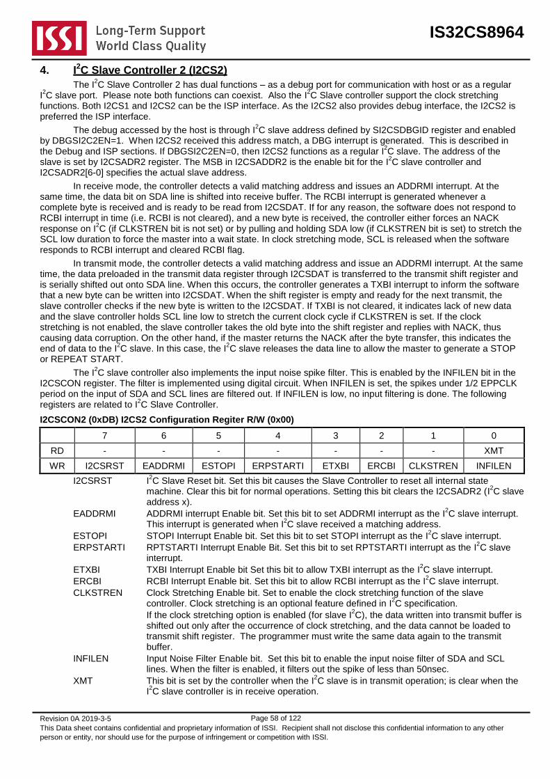
IS32CS8964
Revision 0A 2019-3-5
This Data sheet contains confidential and proprietary information of ISSI. Recipient shall not disclose this confidential information to any other
person or entity, nor should use for the purpose of infringement or competition with ISSI.
Page 58 of 122
4. I2C Slave Controller 2 (I2CS2)
The I2C Slave Controller 2 has dual functions – as a debug port for communication with host or as a regular
I2C slave port. Please note both functions can coexist. Also the I
2C Slave controller support the clock stretching
functions. Both I2CS1 and I2CS2 can be the ISP interface. As the I2CS2 also provides debug interface, the I2CS2 is preferred the ISP interface.
The debug accessed by the host is through I2C slave address defined by SI2CSDBGID register and enabled
by DBGSI2C2EN=1. When I2CS2 received this address match, a DBG interrupt is generated. This is described in the Debug and ISP sections. If DBGSI2C2EN=0, then I2CS2 functions as a regular I
2C slave. The address of the
slave is set by I2CSADR2 register. The MSB in I2CSADDR2 is the enable bit for the I2C slave controller and
I2CSADR2[6-0] specifies the actual slave address.
In receive mode, the controller detects a valid matching address and issues an ADDRMI interrupt. At the same time, the data bit on SDA line is shifted into receive buffer. The RCBI interrupt is generated whenever a complete byte is received and is ready to be read from I2CSDAT. If for any reason, the software does not respond to RCBI interrupt in time (i.e. RCBI is not cleared), and a new byte is received, the controller either forces an NACK response on I
2C (if CLKSTREN bit is not set) or by pulling and holding SDA low (if CLKSTREN bit is set) to stretch the
SCL low duration to force the master into a wait state. In clock stretching mode, SCL is released when the software responds to RCBI interrupt and cleared RCBI flag.
In transmit mode, the controller detects a valid matching address and issue an ADDRMI interrupt. At the same time, the data preloaded in the transmit data register through I2CSDAT is transferred to the transmit shift register and is serially shifted out onto SDA line. When this occurs, the controller generates a TXBI interrupt to inform the software that a new byte can be written into I2CSDAT. When the shift register is empty and ready for the next transmit, the slave controller checks if the new byte is written to the I2CSDAT. If TXBI is not cleared, it indicates lack of new data and the slave controller holds SCL line low to stretch the current clock cycle if CLKSTREN is set. If the clock stretching is not enabled, the slave controller takes the old byte into the shift register and replies with NACK, thus causing data corruption. On the other hand, if the master returns the NACK after the byte transfer, this indicates the end of data to the I
2C slave. In this case, the I
2C slave releases the data line to allow the master to generate a STOP
or REPEAT START.
The I2C slave controller also implements the input noise spike filter. This is enabled by the INFILEN bit in the
I2CSCON register. The filter is implemented using digital circuit. When INFILEN is set, the spikes under 1/2 EPPCLK period on the input of SDA and SCL lines are filtered out. If INFILEN is low, no input filtering is done. The following registers are related to I
2C Slave Controller.
I2CSCON2 (0xDB) I2CS2 Configuration Regiter R/W (0x00)
7 6 5 4 3 2 1 0
RD - - - - - - - XMT
WR I2CSRST EADDRMI ESTOPI ERPSTARTI ETXBI ERCBI CLKSTREN INFILEN
I2CSRST I2C Slave Reset bit. Set this bit causes the Slave Controller to reset all internal state
machine. Clear this bit for normal operations. Setting this bit clears the I2CSADR2 (I2C slave
address x).
EADDRMI ADDRMI interrupt Enable bit. Set this bit to set ADDRMI interrupt as the I2C slave interrupt.
This interrupt is generated when I2C slave received a matching address.
ESTOPI STOPI Interrupt Enable bit. Set this bit to set STOPI interrupt as the I2C slave interrupt.
ERPSTARTI RPTSTARTI Interrupt Enable Bit. Set this bit to set RPTSTARTI interrupt as the I2C slave
interrupt.
ETXBI TXBI Interrupt Enable bit Set this bit to allow TXBI interrupt as the I2C slave interrupt.
ERCBI RCBI Interrupt Enable bit. Set this bit to allow RCBI interrupt as the I2C slave interrupt.
CLKSTREN Clock Stretching Enable bit. Set to enable the clock stretching function of the slave controller. Clock stretching is an optional feature defined in I
2C specification.
If the clock stretching option is enabled (for slave I2C), the data written into transmit buffer is
shifted out only after the occurrence of clock stretching, and the data cannot be loaded to transmit shift register. The programmer must write the same data again to the transmit buffer.
INFILEN Input Noise Filter Enable bit. Set this bit to enable the input noise filter of SDA and SCL lines. When the filter is enabled, it filters out the spike of less than 50nsec.
XMT This bit is set by the controller when the I2C slave is in transmit operation; is clear when the
I2C slave controller is in receive operation.

IS32CS8964
Revision 0A 2019-3-5
This Data sheet contains confidential and proprietary information of ISSI. Recipient shall not disclose this confidential information to any other
person or entity, nor should use for the purpose of infringement or competition with ISSI.
Page 59 of 122
I2CSST2 (0xDC) I2CS2 Status Register R/W (0x00)
7 6 5 4 3 2 1 0
RD FIRSTBT ADDRMI STOPI RPSTARTI TXBI RCBI START NACK
WR - ADDRMI STOPI RPSTARTI HOLDT[3] HOLDT[2] HOLDT[1] HOLDT[0]
FIRSTBT This bit is set to indicate the data in the data register as the first byte received after address match. This bit is cleared after the first byte of the transaction is read. The bit is read only and generated by the slave controller.
ADDRMI Slave Address Match Interrupt Flag bit. This bit is set when the received address matches the address defined in I2CSADR2. If EADDMI is set, this generates an interrupt. This bit must be cleared by software.
STOPI Stop Condition Interrupt Flag bit. This bit is set when the slave controller detects a STOP condition on the SCL and SDA lines. This bit must be cleared by software.
RPTSARTI Repeat Start Condition Interrupt Flag bit. This bit is set when the slave controller detects a REPEAT START condition on the SCL and SDA lines. This bit must be cleared by software.
TXBI Transmit Buffer Interrupt Flag. This bit is set when the slave controller is ready to accept a new byte for transmit. This bit is cleared when new data is written into I2CSDAT register.
RCBI Receiver Buffer Interrupt Flag bit. This bit is set when the slave controller puts new data in the I2CSDAT and ready for software-reading. This bit is cleared after the software reads I2CSDAT.
START Start Condition. This bit is set when the slave controller detects a START condition on the SCL and SDA lines. This bit is not very useful as the start of transaction can be indicated by address match interrupt. This read-only bit is cleared when STOP condition is detected.
NACK NACK Condition. This bit is set when the host responds with NACK in the byte transaction. This bit is only meaningful for slave-transmit operation. Please note if the master returns with NACK on the byte transaction, the slave does not upload new data into the shift register. And the slave transmits the old data again as the next transfer, and this re-transmission continues if NACK is repeated until the transmission is successful and returned with ACK. This bit is cleared when a new ACK is detected or the start condition.
HOLDT[3-0] These four bits define the hold time of the peripheral clock (EPPCLK) cycles between SDA to SCL. The I
2C specification requires for minimum of 300nsec hold time, so the condition
of “TEPPCLK*(HOLDT[3:0]+3) ≧300nsec hold time” equation must be met. For example, if
the peripheral clock cycle (EPPCLK) is 20MHz, then HOLD[3-0] should be set to ≧3.
I2CSADR2 (0xDD) I2CS2 Slave Address Register R/W (0x00)
7 6 5 4 3 2 1 0
RD - - - - - - - -
WR I2CSEN ADDR[6-0]
I2CSENT Set this bit to enable the I2C slave controller.
ADDR[6-0] 7-bit slave address.
I2CSDAT2 (0xDE) I2CS2 Data Register R/W (0x00)
7 6 5 4 3 2 1 0
RD I2C Slave Receive Data Register
WR I2C Slave Transmit Data Register

IS32CS8964
Revision 0A 2019-3-5
This Data sheet contains confidential and proprietary information of ISSI. Recipient shall not disclose this confidential information to any other
person or entity, nor should use for the purpose of infringement or competition with ISSI.
Page 60 of 122
5. EUART2 with LIN Controller (EUART2)
LIN-capable 16550-like EUART2 is an enhanced UART controller (EUART) with separate transmit and receive FIFO. Both transmit and receive FIFO are 15-bytes deep and can be parameterized for interrupt triggering. The addition of FIFO significantly reduces the CPU load to handle high-speed serial interface. Transmit FIFO and receive FIFO have respective interrupt trigger levels that can be set based on optimal CPU performance adjustment. The EUART2 also has dedicated 16-bit Baud Rate generator and thus provides accurate baud rate under wide range of system clock frequency. The EUART2 also provides LIN extensions that incorporate message handling and baud-rate synchronization. The block diagram of EUART2 is shown in the following.
EUART_LINephclk
rsto
ramsfrdatao[7:0]
ramsfraddr[6:0]
sfroe
ephsfrwe
euart_rxd
sfrdatai[7:0]
euart_into
euart_txd
sfr_active
xaddr[15:0]
xdin[7:0]
xwr
xrd
lin_int
lin_xdout[7:0]
lin_xfr_active
lin_controller
LCTRL (A090H)
SBRL (A094H)
SBRH (A093H)
LINT (A095H)
LINTEN (A090H)
16-bit Counter
LCNTRH (A091h)
LCNTRL (A092h)
FSM
rx_rise
rx_fall
EUART_RCV
EUART_TX
send_break_o
rx_sync_byte
euart_si
sync_timeout
EUART_REGS
divisor[15:0] BR[15:0]divisor[15:0]
Load (start or rx_baud_out)
16-bit down counter
baudrate_cntr[15:0]
rx_baud_out =
(baudrate_cntr == 16'h00)
inh_rx_fifo
lin_en
The following registers are used for configurations of and interface with EUART2.
SCON2 (0xC2) UART2 Configuration Register 00000000, R/W
7 6 5 4 3 2 1 0
RD EUARTEN SB WLS[1] WLS[0] BREAK OP PERR SP
WR EUARTEN SB WLS[1] WLS[0] BREAK OP PE SP
EUARTEN Transmit and Receive Enable bit
Set to enable EUART2 transmit and receive functions: To transmit messages in the TX FIFO and to store received messages in the RX FIFO.
SB Stop Bit Control
Set to enable 2 Stop bits, and clear to enable 1 Stop bit.

IS32CS8964
Revision 0A 2019-3-5
This Data sheet contains confidential and proprietary information of ISSI. Recipient shall not disclose this confidential information to any other
person or entity, nor should use for the purpose of infringement or competition with ISSI.
Page 61 of 122
WLS[1-0] The number of bits of a data byte. This does not include the parity bit when parity is enabled.
00 - 5 bits
01 - 6 bits
10 - 7 bits
11 - 8 bits
BREAK Break Condition Control Bit.
Set to initiate a break condition on the UART interface by holding UART output at low until BREAK bit is cleared.
OP Odd/Even Parity Control Bit (0 = Even, 1 = Odd)
PE/PERR Parity Enable / Parity Error status
Set to enable parity and clear to disable parity checking functions. If read, PERR=1 indicates a parity error in the current data of RX FIFO.
SP Parity Set Control Bit
When SP is set, the parity bit is always transmitted as 1.
SFIFO2 (0xA5) UART2 FIFO Status/Control Register 00000000 R/W
7 6 5 4 3 2 1 0
RD RFL[3-0] TFL[3-0]
WR RFLT[33-0] TFLT[3-0]
RFL[3-0] Current Receive FIFO level. This is read only and indicate the current receive FIFO byte count.
RFLT[3-0] Receive FIFO trigger threshold. This is write-only. RDA interrupt will be generated when RFL[3-0] is greater than RFLT[3-0].
RFLT[3-0] Description
0000 RX FIFO trigger level = 0
0001 RX FIFO trigger level = 1
0010 RX FIFO trigger level = 2
0011 RX FIFO trigger level = 3
0100 RX FIFO trigger level = 4
0101 RX FIFO trigger level = 5
0110 RX FIFO trigger level = 6
0111 RX FIFO trigger level = 7
1000 RX FIFO trigger level = 8
1001 RX FIFO trigger level = 9
1010 RX FIFO trigger level = 10
1011 RX FIFO trigger level = 11
1100 RX FIFO trigger level = 12
1101 RX FIFO trigger level = 13
1110 RX FIFO trigger level = 14
1111 Reserved
TFL[3-0] Current Transmit FIFO level. This is read only and indicate the current transmit FIFO byte count.

IS32CS8964
Revision 0A 2019-3-5
This Data sheet contains confidential and proprietary information of ISSI. Recipient shall not disclose this confidential information to any other
person or entity, nor should use for the purpose of infringement or competition with ISSI.
Page 62 of 122
TFLT[3-0] Transmit FIFO trigger threshold. This is write-only. TRA interrupt will be generated when TFL[3-0] is less than TFLT[3-0].
TFLT[3-0] Description
0000 Reserved
0001 TX FIFO trigger level = 1
0010 TX FIFO trigger level = 2
0011 TX FIFO trigger level = 3
0100 TX FIFO trigger level = 4
0101 TX FIFO trigger level = 5
0110 TX FIFO trigger level = 6
0111 TX FIFO trigger level = 7
1000 TX FIFO trigger level = 8
1001 TX FIFO trigger level = 9
1010 TX FIFO trigger level = 10
1011 TX FIFO trigger level = 11
1100 TX FIFO trigger level = 12
1101 TX FIFO trigger level = 13
1110 TX FIFO trigger level = 14
1111 TX FIFO trigger level = 15
Receive and transmit FIFO can be reset by clear FIFO operation. This is done by setting BR[11-0]=0 and EUARTEN=0. This also clears RFO, RFU and TFO interrupt flags without writing the interrupt register. The LIN counter LCNTR is also cleared.
SINT2 (0xA7) UART2 Interrupt Status/Enable Register 00000000 R/W
7 6 5 4 3 2 1 0
RD INTEN TRA RDA RFO RFU TFO FERR TI
WR INTEN TRAEN RDAEN RFOEN RFUEN TFOEN FERREN TIEN
INTEN Interrupt Enable bit. Write only
Set to enable UART2 interrupt. Clear to disable interrupt. Default is 0.
TRA/TRAEN Transmit FIFO is ready to be filled.
This bit is set when transmit FIFO has been emptied below FIFO threshold. Write “1” to enable interrupt. The flag is automatically cleared when the condition is absent.
RDA/RDAEN Receive FIFO is ready to be read.
This bit is set by hardware when receive FIFO has been filled above the FIFO threshold. Write “1” to enable interrupt. RDA will also be set when RFL < RFLT for bus idle duration longer than RFLT * 16 * Baud Rate. This is to inform software that there are still remaining unread received bytes in the FIFO.
This flag is cleared when RFL < RFLT and writing “0” on the bit (the interrupt is disabled simultaneously).
RFO/RFOEN Receive FIFO Overflow Enable bit
This bit is set when overflow condition of receive FIFO occurs. Write “1” to enable interrupt. The flag can be cleared by software, writing “0” on the bit (the interrupt is disabled simultaneously), or by FIFO reset action.
RFU/RFUEN Receive FIFO Underflow Enable bit
This bit is set when underflow condition of receive FIFO occurs. Write “1” to enable interrupt. The flag can be cleared by software, writing “0” on the bit (the interrupt is disabled simultaneously), or by FIFO reset action.
TFO/TFOEN Transmit FIFO Overflow Interrupt Enable bit
This bit is set when overflow condition of transmit FIFO occurs. Write “1” to enable interrupt. The flag can be cleared by software, writing “0” on the bit (the interrupt is disabled simultaneously), or by FIFO reset action.

IS32CS8964
Revision 0A 2019-3-5
This Data sheet contains confidential and proprietary information of ISSI. Recipient shall not disclose this confidential information to any other
person or entity, nor should use for the purpose of infringement or competition with ISSI.
Page 63 of 122
FERR/FERREN Framing Error Enable bit
This bit is set when framing error occurs as the byte is received. Write “1” to enable interrupt. The flag must be cleared by software, writing “0” on the bit (the interrupt is disabled simultaneously).
TI/TIEN Transmit Message Completion Interrupt Enable bit
This bit is set when all messages in the TX FIFO are transmitted and thus the TX FIFO becomes empty. Write “1” to enable interrupt. The flag must be cleared by software, writing “0” on the bit (the interrupt is disabled simultaneously).
SBUF2 (0xA6) UART2 Data Buffer Register 0x00 R/W
7 6 5 4 3 2 1 0
RD EUART2 Receive Data Register
WR EUART2 Transmit Data Register
This register is the virtual data buffer register for both receive and transmit FIFO. When being read, it reads out the top byte of the RX FIFO; when being written, it writes into the top byte of the TX FIFO.
EUART2 can be configured to add LIN capability. The major enhancement of LIN includes master/slave configurations, auto baud-rate synchronization, and frame based protocol with header. Under LIN extension mode, all EUART2 registers and functions are still effective and operational. LIN is a single-wire bus and it requires external components to combine RX and TX signals externally. LIN is frame based and consists of message protocols with master/slave configurations. The following diagram shows the basic composition of a header message sent by the master. It starts with BREAK field, the SYNC field, PID field, DATA bytes, and CRC bytes. The LIN controller can handle the BREAK field and the SYNC field by hardware, for the PID field, DATA bytes and CRC bytes must be processed by software.
11 bit times
Break Break
delimiter
IDLE BREAK BREAK_OK BREAK_DEL
Start
bit
LSB
(bit 0)
MSB
(bit 7)Stop
bit
Byte field
BREAK_DEL SYNC_S SYNC_0 SYNC_1 SYNC_2 SYNC_3 SYNC_4 IDLE
A LIN frame structure is shown and the frame time matches the number of bits sent and has a fixed timing.
LIN bus protocol is based on frame. Each frame is partitioned into several parts as shown above. For master to initiate a frame, the software follows the following procedure.
Initiate a SBK command. (SW needs to check if the bus is in idle state, and there is no pending transmit data).
Write “55” into TFIFO.
Write “PID” into TFIFO.
Wait for SBK to complete interrupts and then write the following transmit data if applicable. (This is optional).
The following diagram shows Finite State Machine (FSM) of the LIN extension and is followed by registers within EUART2.

IS32CS8964
Revision 0A 2019-3-5
This Data sheet contains confidential and proprietary information of ISSI. Recipient shall not disclose this confidential information to any other
person or entity, nor should use for the purpose of infringement or competition with ISSI.
Page 64 of 122
IDLE
BREAK
BREAK_OK
BREAK_
DEL
SYNC_S
SYNC_0
SYNC_1
SYNC_2
SYNC_3
SYNC_4
TX_BREAK
TX_BREAK
_DEL
rx_rise
lcntr[3:0] == 4'hB
rx_fall & ~mas_en send_break & mas_en
lcntr[4:0] == bk_len[2:0] + 4'hD
sync_timeout
sync_timeout
sync_timeout
sync_timeout
rx_rise
rx_fall
rx_rise
rx_rise
rx_fall
rx_fall
sync_timeout
lcntr[5]
rx_rise
rx_baud_out
reset or ~LINEN
if data_reg[7:4] == 4'h5
rx_sync_ok <= 1'b1
sync_baud_reg <=
(lcntr/16)/4
inh_rx_fifo <= 1'b1
Clear LIN
Counter
(count in sysclk)
Clear LIN
Counter
(count in sysclk)
Clear LIN
Counter
(count in sysclk)
Clear LIN
Counter
(count in sysclk)
send_break <= 1'b0
tx_break_ok <= 1'b1lcntr[5]
sync_timeout
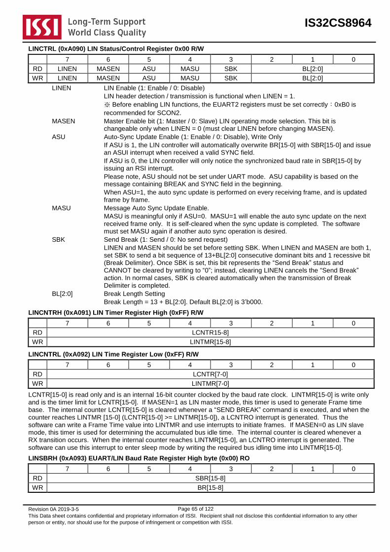
IS32CS8964
Revision 0A 2019-3-5
This Data sheet contains confidential and proprietary information of ISSI. Recipient shall not disclose this confidential information to any other
person or entity, nor should use for the purpose of infringement or competition with ISSI.
Page 65 of 122
LINCTRL (0xA090) LIN Status/Control Register 0x00 R/W
7 6 5 4 3 2 1 0
RD LINEN MASEN ASU MASU SBK BL[2:0]
WR LINEN MASEN ASU MASU SBK BL[2:0]
LINEN LIN Enable (1: Enable / 0: Disable)
LIN header detection / transmission is functional when LINEN = 1.
※ Before enabling LIN functions, the EUART2 registers must be set correctly:0xB0 is
recommended for SCON2.
MASEN Master Enable bit (1: Master / 0: Slave) LIN operating mode selection. This bit is changeable only when LINEN = 0 (must clear LINEN before changing MASEN).
ASU Auto-Sync Update Enable (1: Enable / 0: Disable), Write Only
If ASU is 1, the LIN controller will automatically overwrite BR[15-0] with SBR[15-0] and issue an ASUI interrupt when received a valid SYNC field.
If ASU is 0, the LIN controller will only notice the synchronized baud rate in SBR[15-0] by issuing an RSI interrupt.
Please note, ASU should not be set under UART mode. ASU capability is based on the message containing BREAK and SYNC field in the beginning.
When ASU=1, the auto sync update is performed on every receiving frame, and is updated frame by frame.
MASU Message Auto Sync Update Enable.
MASU is meaningful only if ASU=0. MASU=1 will enable the auto sync update on the next received frame only. It is self-cleared when the sync update is completed. The software must set MASU again if another auto sync operation is desired.
SBK Send Break (1: Send / 0: No send request)
LINEN and MASEN should be set before setting SBK. When LINEN and MASEN are both 1, set SBK to send a bit sequence of 13+BL[2:0] consecutive dominant bits and 1 recessive bit (Break Delimiter). Once SBK is set, this bit represents the “Send Break” status and CANNOT be cleared by writing to “0”; instead, clearing LINEN cancels the “Send Break” action. In normal cases, SBK is cleared automatically when the transmission of Break Delimiter is completed.
BL[2:0] Break Length Setting
Break Length = 13 + BL[2:0]. Default BL[2:0] is 3’b000.
LINCNTRH (0xA091) LIN Timer Register High (0xFF) R/W
7 6 5 4 3 2 1 0
RD LCNTR15-8]
WR LINTMR[15-8]
LINCNTRL (0xA092) LIN Time Register Low (0xFF) R/W
7 6 5 4 3 2 1 0
RD LCNTR[7-0]
WR LINTMR[7-0]
LCNTR[15-0] is read only and is an internal 16-bit counter clocked by the baud rate clock. LINTMR[15-0] is write only and is the timer limit for LCNTR[15-0]. If MASEN=1 as LIN master mode, this timer is used to generate Frame time base. The internal counter LCNTR[15-0] is cleared whenever a “SEND BREAK” command is executed, and when the counter reaches LINTMR [15-0] (LCNTR[15-0] >= LINTMR[15-0]), a LCNTRO interrupt is generated. Thus the software can write a Frame Time value into LINTMR and use interrupts to initiate frames. If MASEN=0 as LIN slave mode, this timer is used for determining the accumulated bus idle time. The internal counter is cleared whenever a RX transition occurs. When the internal counter reaches LINTMR[15-0], an LCNTRO interrupt is generated. The software can use this interrupt to enter sleep mode by writing the required bus idling time into LINTMR[15-0].
LINSBRH (0xA093) EUART/LIN Baud Rate Register High byte (0x00) RO
7 6 5 4 3 2 1 0
RD SBR[15-8]
WR BR[15-8]

IS32CS8964
Revision 0A 2019-3-5
This Data sheet contains confidential and proprietary information of ISSI. Recipient shall not disclose this confidential information to any other
person or entity, nor should use for the purpose of infringement or competition with ISSI.
Page 66 of 122
LINSBRL (0xA094) EUART/LIN Baud Rate Register Low byte (0x00) RO
7 6 5 4 3 2 1 0
RD SBR[7:0]
WR BR[7-0]
SBR[15-0] The acquired Baud Rate under LIN protocol. This is read-only.
SBR[15-0] is the acquired baud rate from last received valid sync byte. SBR is meaningful only in LIN-Slave mode.
BR[15-0] The Baud Rate Setting of EUART/LIN. This is write-only. BR[15-0] can not be 0.
BUAD RATE = SYSCLK/BR[15-0].
When a slave receives a BREAK followed by a valid SYNC field, an RSI interrupt is generated and the acquired baud rate from SYNC field is stored in SBR[15-0]. The acquired baud rate is BAUD RATE = SYSCLK/SBR[15-0]. The software can just update this acquired value into BR[15-0] to achieve synchronization with the master. If Auto-Sync Update (ASU) register bit is enabled under LIN slave mode, LIN controller will automatically perform the update of BR[15-0] with SBR[15-0] and issue another ASUI interrupt when received a valid SYNC field.
LININT (0xA095) LIN Interrupt Flag Register (0x00) R/W
7 6 5 4 3 2 1 0
RD - - LSTAT LIDLE ASUI SBKI RSI LCNTRO
WR - - - - ASUI SBKI RSI LCNTRO
LSTAT LIN Bus Status bit (1: Recessive / 0: Dominant), Read only.
LSTAT = 1 indicates that the LIN bus (RX pin) is in recessive state.
LIDLE LIDLE is 1 when LIN bus is idle and not transmitting/receiving LIN header or data bytes. This bit read only. It is 1 when LINEN = 0.
ASUI Auto-Sync Updated completion Interrupt (1: Set / 0: Clear)
This flag is set when auto baud rate synchronization has been completed and BR[15-0] has been updated with SBR[15-0] by hardware. It must be cleared by writing “1” on the bit.
SBKI Send Break Completion Interrupt bit (1: Set / 0: Clear)
This flag is set when Send Break completes. It must be cleared by writing “1” in the bit.
RSI Receive Sync Completion Interrupt bit (1: Set / 0: Clear)
This flag is set when a valid Sync byte is received following a Break. It must be cleared by writing “1” in the bit.
LCNTRO LIN Counter Overflow Interrupt bit (1: Set / 0: Clear).
This flag is set when the LIN counter reaches 0xFFFF. It must be cleared by writing “1” in the bit.
LININTEN (0xA096) LIN Interrupt Enable Register (0x00) R/W
7 6 5 4 3 2 1 0
RD LINTEN - - - ASUIE SBKIE RSIE LCNTRIE
WR LINTEN - - - ASUIE SBKIE RSIE LCNTRIE
LINTEN LIN Interrupt Enable (1: Enable / 0: Disable)
Set to enable all LIN interrupts. LINT flags should be checked before setting or modifying.
ASUIE Auto-Sync Update Interrupt Enable (1: Enable / 0: Disable)
SBKIE Send Break Completion Interrupt Enable (1: Enable / 0: Disable)
RSIE Receive Sync Completion Interrupt Enable (1: Enable / 0: Disable)
LCNTRIE LIN Counter Overflow Interrupt Enable (1: Enable / 0: Disable)

IS32CS8964
Revision 0A 2019-3-5
This Data sheet contains confidential and proprietary information of ISSI. Recipient shall not disclose this confidential information to any other
person or entity, nor should use for the purpose of infringement or competition with ISSI.
Page 67 of 122
6. Serial Peripheral Interface (SPI)
The Serial Peripheral Interface (SPI) is an enhanced synchronous serial hardware which is compatible with Motorola’s SPI specifications. The SPI Controller includes 4-bytes FIFO for both transmit and receive. SPI Interface uses Master-Out-Slave-In (MOSI), Master-In-Slave-Out (MISO), Serial Clock (SCK) and Slave Select (SSN) for interface. SSN is low active and only meaningful in slave mode.
SPICR (0xA1) SPI Configuration Register R/W (0b001000xx)
7 6 5 4 3 2 - 0
RD SPIE SPEN MSTR CPOL CPHA SCKE - -
WR SPIE SPEN MSTR CPOL CPHA SCKE - -
SPIE SPI interface Interrupt Enable bit.
SPEN SPI interface Enable bit.
MSTR SPI Master/Slave Switch.(set as a master; clear as a slave)
CPOL SPI interface Polarity bit: Set to configure the SCK to stay HIGH while the SPI interface is idling and clear to keep it LOW.
CPHA Clock Phase Control bit: If CPOL=0, set to shift output data at rising edge of SCK, and clear to shift output data at falling edge of SCK. If CPOL=1, set to shift output data at falling edge of SCK and clear to shift output data at rising edge of SCK.
SCKE Clock Selection bit in Master Mode: Set to use rising edge of SCK to sample the input data. Clear to use falling edge of SCK to sample the input data.
In Slave mode, the sampling phase is determined by the combinations of CPOL and CPHA setting shown in the following table.
CPOL CPHA (Slave mode) SCK edge used for sampling input data Data shift out
0 0 Rising edge Falling edge
0 1 Falling edge Rising edge
1 0 Falling edge Rising edge
1 1 Rising edge Falling edge
SPIMR (0xA2) SPI Mode Control Register R/W (0x00)
7 6 5 4 3 2 1 0
RD ICNT1 ICNT0 FCLR - SPR[2] SPR[1] SPR[0] DIR
WR ICNT1 ICNT0 FCLR - SPR[2] SPR[1] SPR[0] DIR
ICNT1, ICNT0 FIFO Byte Count Threshold.
This sets the FIFO threshold for generating SPI interrupts.
00 – the interrupt is generated after 1 byte is sent or received;
01 – the interrupt is generated after 2 bytes are sent or received;
10 – the interrupt is generated after 3 bytes are sent or received;
11 – the interrupt is generated after 4 bytes are sent or received.
FCLR FIFO Clear/Reset
Set to clear and reset transmit and receive FIFO
SPR[2-0] SPI Clock Rate Setting. This is used to control the SCK clock rate of SPI interface.
000 – SCK = SYSCLK/6;
001 – SCK = SYSCLK/8;
010 – SCK = SYSCLK/16;
011 – SCK = SYSCLK/32;
100 – SCK = SYSCLK/64;
101 – SCK = SYSCLK/128;
110 – SCK = SYSCLK/256;
111 – SCK = SYSCLK/512.
DIR Transfer Format
DIR=1 uses MSB-first format.
DIR=0 uses LSB-first format.

IS32CS8964
Revision 0A 2019-3-5
This Data sheet contains confidential and proprietary information of ISSI. Recipient shall not disclose this confidential information to any other
person or entity, nor should use for the purpose of infringement or competition with ISSI.
Page 68 of 122
SPIST (0xA3) SPI Status Register R/W (0x00)
7 6 5 4 3 2 1 0
RD SSPIF ROVR TOVR TUDR RFULL REMPT TFULL TEMPT
WR SSPIF ROVR TOVR TUDR - - - -
SSPIF SPI Interrupt Flag bit. Set by hardware to indicate the completion of data transfer. Clear by assigning this bit to 0 or disabling SPI.
ROVR Receive FIFO-overrun Error Flag bit. When Receiver FIFO Full Status occurs and SPI receives new data, ROVR is set and generates an interrupt. Clear by assigning this bit to 0 or disabling SPI.
TOVR Transmit FIFO-overrun Error Flag bit. When Transfers FIFO Full Status occurs and new data is written, TOVR is set and generates an interrupt. Clear by assigning this bit to 0 or disabling SPI.
TUDR Transmit Under-run Error Flag bit. When Transfers FIFO Empty Status and new data transmission occur, TUDR is set and generates an interrupt. Clear by written 0 to this bit or disable SPI.
RFULL Receive FIFO Full Status bit . Set when receiver FIFO is full. Read only.
REMPT Receive FIFO Empty Status bit . Set when receiver FIFO is empty. Read only.
TFULL Transmitter FIFO Full Status bit . Set when transfer FIFO is full. Read only.
TEMPT Transmitter FIF0 Empty Status bit . Set when transfer FIFO is empty. Read only.
SPIDAT (0xA4) SPI Data Register R/W (0xXX)
7 6 5 4 3 2 1 0
RD SPI Receive Data Register
WR SPI Transmit Data Register
6.1 SPI Master Timing Illustration
6.1.1 CPOL=0 CPHA=0
bit7 bit6 bit5 bit4 bit3 bit2 bit1 bit0
SPI MODE TIMING, MASTER MODE
SPEN
SCK(CPOL=0, CPHA=0)
MOSI
MISO (SCKE=1)
MISO (SCKE=0)
SSPIF
bit7
bit7
bit0
bit0

IS32CS8964
Revision 0A 2019-3-5
This Data sheet contains confidential and proprietary information of ISSI. Recipient shall not disclose this confidential information to any other
person or entity, nor should use for the purpose of infringement or competition with ISSI.
Page 69 of 122
6.1.2 CPOL=0 CPHA=1
bit7 bit6 bit5 bit4 bit3 bit2 bit1 bit0
SPI MODE TIMING, MASTER MODE
SPEN
SCK(CPOL=0, CPHA=1)
MOSI
MISO (SCKE=1)
MISO (SCKE=0)
SSPIF
bit7
bit7
bit0
bit0
6.1.3 CPOL=1 CPHA=0
bit7 bit6 bit5 bit4 bit3 bit2 bit1 bit0
SPI MODE TIMING, MASTER MODE
SPEN
SCK(CPOL=1, CPHA=0)
MOSI
MISO (SCKE=0)
MISO (SCKE=1)
SSPIF
bit7
bit7
bit0
bit0
6.1.4 CPOL=1 CPHA=1
bit7 bit6 bit5 bit4 bit3 bit2 bit1 bit0
SPI MODE TIMING, MASTER MODE
SPEN
SCK(CPOL=1, CPHA=1)
MOSI
MISO (SCKE=0)
MISO (SCKE=1)
SSPIF
bit7
bit7
bit0
bit0
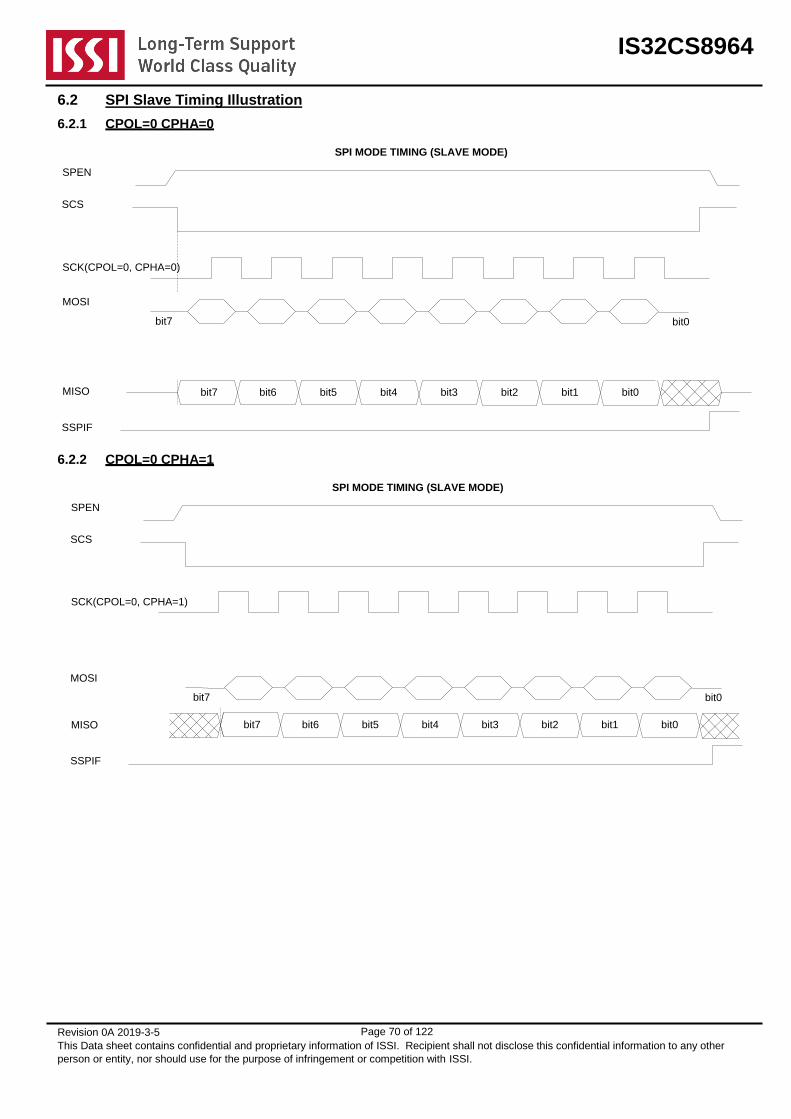
IS32CS8964
Revision 0A 2019-3-5
This Data sheet contains confidential and proprietary information of ISSI. Recipient shall not disclose this confidential information to any other
person or entity, nor should use for the purpose of infringement or competition with ISSI.
Page 70 of 122
6.2 SPI Slave Timing Illustration
6.2.1 CPOL=0 CPHA=0
bit7 bit6 bit5 bit4 bit3 bit2 bit1 bit0
SPI MODE TIMING (SLAVE MODE)
SPEN
MISO
MOSI
SSPIF
bit7 bit0
SCK(CPOL=0, CPHA=0)
SCS
6.2.2 CPOL=0 CPHA=1
bit7 bit6 bit5 bit4 bit3 bit2 bit1 bit0
SPI MODE TIMING (SLAVE MODE)
SPEN
MISO
MOSI
SSPIF
bit7 bit0
SCK(CPOL=0, CPHA=1)
SCS
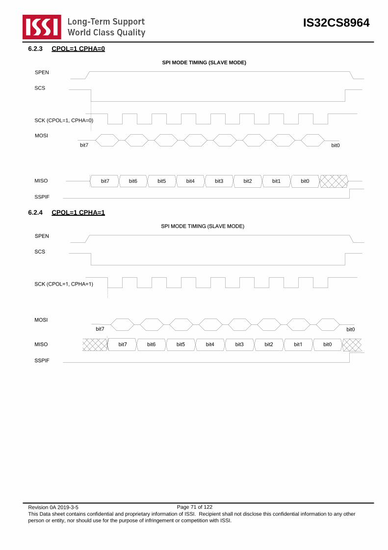
IS32CS8964
Revision 0A 2019-3-5
This Data sheet contains confidential and proprietary information of ISSI. Recipient shall not disclose this confidential information to any other
person or entity, nor should use for the purpose of infringement or competition with ISSI.
Page 71 of 122
6.2.3 CPOL=1 CPHA=0
SPI MODE TIMING (SLAVE MODE)
SPEN
MOSI
SSPIF
bit7 bit0
SCS
MISO bit7 bit6 bit5 bit4 bit3 bit2 bit1 bit0
SCK (CPOL=1, CPHA=0)
6.2.4 CPOL=1 CPHA=1
SPI MODE TIMING (SLAVE MODE)
SPEN
MOSI
SSPIF
bit7 bit0
SCS
MISO
SCK (CPOL=1, CPHA=1)
bit7 bit6 bit5 bit4 bit3 bit2 bit1 bit0

IS32CS8964
Revision 0A 2019-3-5
This Data sheet contains confidential and proprietary information of ISSI. Recipient shall not disclose this confidential information to any other
person or entity, nor should use for the purpose of infringement or competition with ISSI.
Page 72 of 122
7. Programmable Counter Array (PCA) and Compare/Capture/PWM (CCP)
The PCA provides enhanced timing functions with less CPU intervention than the standard 8051 timers T0, T1, and T2. The PCA is partitioned in three parts. The main PCA Counter consists of CH and CL. There are 6 channels of Compare/Capture/PWM modules.
8-BIT DIVIDER
PCACPS[7-0]CH[7-0] CL[7-0]
CHRLD[7-0] CLRLD[7-0]
AUTO RELOAD
CHSR[7-0] CLSR[7-0]
CL READ SNAPSHOT
CH:CL
CCAPH
CCAPM[7-0] CONFIGURATION
CCAPL
COMPARATOR
CCAP MODULE 5-0
PCACON[7-0]
PCAMOD[7-0]
CHIR[7-0]/DB CLIR[7-0]/DB CHIR:CLIR
==
CH:CL
CIF
The MAIN COUNTER (CH and CL) is configured and controlled by two registers, CMOD and PCACON. The counter value is accessed by CH and CL registers. The counter can be configured as either FREE-RUN or AUTO-RELOADED mode. The counter values of CH and CL can be captured in CHSR and CLSR triggered by software or hardware. There is also a counter compare register CHIR and CHLR. An interrupt can be enabled at CH:CL == CHIR:CLIR. This allows the PCA to easily synchronize with the software control. CHIR and CLIR are double-buffered.
PCACPS (0xA0A5) PCA Counter Clock Scaling Register R/W (0x00)
7 6 5 4 3 2 1 0
RD PCACPS[7-0]
WR PCACPS[7-0]
PCACPS sets the clock input to the PCA at SYSCLK/(PCACPS[7-0]+1).
PCAMOD (0xD1) PCA Mode Control Register R/W (0x00)
7 6 5 4 3 2 1 0
RD CIDL RLDEN COUNT8 OVF8EN PCAEN ECF CIFEN CMPTRIG
WR CIDL RLDEN COUNT8 OVF8EN PCAEN ECF CIFEN CMPTRIG
CIDL Counter Control bit in IDLE mode
When CIDL=1, PCA counting is disabled in IDLE mode.
When CIDL=0, normal counting of PCA in IDLE mode persists. PCAEN needs to be 1 for counting.
RLDEN: AUTO-RELOAD Mode Enable bit
Set RLDEN=1to enable AUTO-RELOAD mode. At overflow, the main counter is reloaded with CHRL and CHRH in 16-bit mode or CHRL in 8-bit mode.
When RLDEN=0: FREE-RUN mode.
COUNT8 8-Bit or 16-Bit Counter Mode Select bit
When COUNT8=1 the PCA is configured as an 8-Bit counter. In 8-bit counter mode, OVF8EN must be set as 1.
COUNT8=0 the PCA is configured as a16-Bit counter
OVF8EN 8-Bit Overflow Enable bit
When OVF8EN=1, the PCA overflow condition occurs at 0xXXFF to 0xXX00. In other words, the overflow condition (CF flag) is set every 256 count. This overflow condition also applies to the 16-bit counter mode.
When OVF8EN=0 the PCA overflow condition occurs at 0xFFFF to 0X0000. This does not work in 16-bit counter mode.
PCAEN PCA counter Enable bit
Set PCAEN=1 to enable the PCA counter
Set PCAEN=0 to disable the PCA and also clears the counter value. When PCAEN=0, all double buffer is loaded with reload values.
IS32CS8964
Revision 0A 2019-3-5
This Data sheet contains confidential and proprietary information of ISSI. Recipient shall not disclose this confidential information to any other
person or entity, nor should use for the purpose of infringement or competition with ISSI.
Page 73 of 122
ECF Counter Overflow Interrupt Flag bit
When ECF=1 the overflow condition interrupt is enabled.
When ECS=0 the overflow interrupt is disabled.
CIFEN Count Compare Interrupt Enable
Set IFEN=1 to enable CHIR:CLIR == CH:CL interrupt
Set IFEN=0 to disable this interrupt
CMPTRIG Comparator Trigger Enable
CMPTRIG=1 enables the snapshot of PCA count value into CHSR by analog comparator interrupt.
CMPTRIG=0 disables the triggering.
PCACON (0xE1) PCA Configuration Register R/W (0x00)
7 6 5 4 3 2 1 0
RD CF CIF CCF5 CCF4 CCF3 CCF2 CCF1 CCF0
WR CF CIF CCF5 CCF4 CCF3 CCF2 CCF1 CCF0
CF Counter Overflow Flag bit
CF is set to 1 by hardware when overflow condition occurs. The overflow condition occurs at either of 0xFFFF to 0x0000 (OVF8EN=0) or 0xXXFF to 0xXX00 (OVF8EN=1). This bit must be cleared by software.
CIF Count Compare Flag bit
CIF is set by hardware when CH:CL == CHIR:CLIR. This bit must be cleared by software.
CCF5 - CCF0 Module Interrupt Flag 5-0
This is set by hardware as its corresponding module generates an interrupt. These bits must be cleared by software.
CH (0xE9) PCA Main Counter High Byte R/W (0x00)
7 6 5 4 3 2 1 0
RD CH[7-0]
WR -
CH holds the upper 8-bit of the main counter value.
CL (0xD9) PCA Main Counter Low Byte R/W (0x00)
7 6 5 4 3 2 1 0
RD CL[7-0]
WR -
CL holds the lower 8-bit of the main counter value. Reading CL triggers a snapshot action to copy CH:CL to CHSR:CLSR.
CHRLD (0xA0A7) PCA Counter CH Reload Value Register R/W (0x00)
7 6 5 4 3 2 1 0
RD CHRLD[7-0]
WR CHRLD[7-0]
This register holds the reload value for CH in AUTO-RELOAD mode.
CLRLD (0xA0A6) PCA Counter CL Reload Value Register R/W (0x00)
7 6 5 4 3 2 1 0
RD CLRLD[7-0]
WR CLRLD[7-0]
This register holds the reload value for CL in AUTO-RELOAD mode.

IS32CS8964
Revision 0A 2019-3-5
This Data sheet contains confidential and proprietary information of ISSI. Recipient shall not disclose this confidential information to any other
person or entity, nor should use for the purpose of infringement or competition with ISSI.
Page 74 of 122
CHSR (0xF3) PCA Snapshot Register of CH RW (0x00)
7 6 5 4 3 2 1 0
RD CHSR[7-0]
WR CHIR[7-0]
CHSR[7-0] CH Snapshot Register. It is read-only.
CHIR[7-0] CH Counter Compare Interrupt . The compare value is double- buffered.
CLSR (0xF2) PCA Snapshot Register of CL RW (0x00)
7 6 5 4 3 2 1 0
RD CLSR[7-0]
WR CLIR[7-0]
CLSR[7-0] CL Snapshot Register. It is read-only.
CLIR[7-0] CL Counter Compare Interrupt The compare value is double-buffered.
The Compare/Capture modules receive the 16-bit count value from the main counter as the time base. Each module is configured by its mode register CCAPMn and contains two 8-bit registers used for comparing value holder or capturing value in storage. There are several basic modes of operation for CCP modules and each CCP module can be configured in the same or different modes.
CCAPMn CCP Module Configuration Register (0xB2, 0xB3, 0xB4, 0xB5, 0xB6, 0xB7) R/W (0x00)
7 6 5 4 3 2 1 0
RD OF ECOM CAPP CAPN MAT TOG PWM ECCF
WR OF ECOM CAPP CAPN MAT TOG PWM ECCF
OF, TOG When the module is configured as Timer/Comparator modes, these two bits determine the output flag status on pin CEX when timer is up or comparison matches. The setting only affects the CEX and does not impact the interrupt generation
OF TOG CEX
0 0 CEX is unchanged.
0 1 CEX toggles.
1 0 CEX change to low (or remains low).
1 1 CEX change to high (or remains high).
When the module is configured as PWM mode, OF is ignored. Set TOG=1 to enable CEX output to high regardless of PWM value.
ECOM Comparator Enable bit. Set to enable comparator function. Clear to disable the comparator.
CAPP Positive Edge Capture bit. Set to use a positive edge as the capture edge. Clear to disable positive edge capture.
CAPN Negative Edge Capture bit. Set to use a negative edge as the capture edge. Clear to disable negative edge capture
MAT Match Control bit. When MAT = 1, a match of CH/CL with CCAPH/CCAPL causes CCF to be set and generates an interrupt. It also enables a compare edge interrupt in WPWM mode.
PWM Pulse Width Modulation bit. Set to enable PWM function. CEX is the PWM output.
ECCF Enable Capture/Compare/PWM Interrupt bit. Set to enable the CCP module n (n = number of the designated module; there are 6 modules in this case) to generate the interrupt.
CCAPnL CCP Compare Value Low Register (0xD2, 0xD4, 0xD6, 0xE2, 0xE4, 0xE6) R/W (0x00)
7 6 5 4 3 2 1 0
RD CCAPnL[7-0]
WR CCAPnL[7-0]
CCAPnL register holds the compare value or capture value. It is used as PWM value register.

IS32CS8964
Revision 0A 2019-3-5
This Data sheet contains confidential and proprietary information of ISSI. Recipient shall not disclose this confidential information to any other
person or entity, nor should use for the purpose of infringement or competition with ISSI.
Page 75 of 122
CCAPnH CCP Compare Value High Register (0xD3, 0xD5, 0xD7, 0xE3, 0xE5, 0xE7) R/W (0x00)
7 6 5 4 3 2 1 0
RD CCAPnH[7-0]
WR CCAPnH[7-0]
CCAPnH register holds the compare value or capture value. It is used as PWM value register.
7.1 16-Bit Capture Mode
The capture mode is used to measure the elapse time of an external event between the edges of the enabled external signal when either CAPP or CAPN is set. The external CEX is sampled for transition. When a valid capture edge occurs in CEX, the current CH/CL count value is loaded into CCAPnH and CCAPnL registers. At the same time CCFn in PCACON register is set, and interrupt is generated if enabled. The block diagram of the configuration is shown below:
N-Edge DET
P-Edge DET
CAPP
CAPN
CEX CCAPnH CCAPnL
CH CL
LOAD
CCF
EECF
PCA INT
7.2 16-Bit COMPARE TIMER MODE
The COMPARE TIMER mode can be used as a software timer or to generate a PWM output. This mode is enabled when ECOM is set and CAPP CAPN are set to low. To allow the compare result to be used, MAT/ECCF also needs to be set. The CCAPnH and CCAPnL hold the 16-bit Timer value and are compared against the incrementing value CH and CL from the main counter. The compare value is double-buffered and is updated when the main counter overflows. This prevents any unexpected comparator output during updating a new value to CCAPnH and CCAPnL. When a match occurs, CCF is set and an interrupt is generated. The block diagram of this mode is shown as following.
16-BIT COMPARATOR
CH:CL
EQ
DOUBLE BUFFER
CCAPnH:CCAPnL
RELOAD
FFFF->0000 OVF
MAT
ECCF
OF/TOG
CCF
PCA INT
CEX
The match result can also be used to generate CEX output change. Depending on the CCAPM’s OF and TOG setting, CEX output is changed at the compare-match instant. However, the triggering of the change of CEX does not require MAT qualifier. Using CEX, waveform of precision duty cycle waveform or frequency modulation can be generated. The effect of OF/TOG on CEX is described in CCAPM register. To avoid unwanted glitches or a match condition when updating the CCAPnH and CCAPnL registers, when ECOM is set and the writing to CCAPnL causes ECOM to clear. Writing to CCAPnH sets ECOM to start the comparator. Therefore user program should update CCAPnL first and then CCAPnH. Of course, ECOM bit can be controlled directly through CCAPMn register.
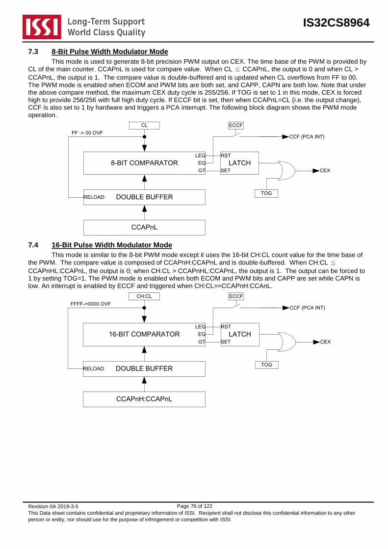
IS32CS8964
Revision 0A 2019-3-5
This Data sheet contains confidential and proprietary information of ISSI. Recipient shall not disclose this confidential information to any other
person or entity, nor should use for the purpose of infringement or competition with ISSI.
Page 76 of 122
7.3 8-Bit Pulse Width Modulator Mode
This mode is used to generate 8-bit precision PWM output on CEX. The time base of the PWM is provided by CL of the main counter. CCAPnL is used for compare value. When CL ≦ CCAPnL, the output is 0 and when CL >
CCAPnL, the output is 1. The compare value is double-buffered and is updated when CL overflows from FF to 00. The PWM mode is enabled when ECOM and PWM bits are both set, and CAPP, CAPN are both low. Note that under the above compare method, the maximum CEX duty cycle is 255/256. If TOG is set to 1 in this mode, CEX is forced high to provide 256/256 with full high duty cycle. If ECCF bit is set, then when CCAPnL=CL (i.e. the output change), CCF is also set to 1 by hardware and triggers a PCA interrupt. The following block diagram shows the PWM mode operation.
8-BIT COMPARATOR
CL
LEQ
DOUBLE BUFFER
CCAPnL
RELOAD
FF -> 00 OVF
GT
LATCH
RST
SET
TOG
CEX
EQ
ECCF
CCF (PCA INT)
7.4 16-Bit Pulse Width Modulator Mode
This mode is similar to the 8-bit PWM mode except it uses the 16-bit CH:CL count value for the time base of
the PWM. The compare value is composed of CCAPnH:CCAPnL and is double-buffered. When CH:CL ≦
CCAPnHL:CCAPnL, the output is 0; when CH:CL > CCAPnHL:CCAPnL, the output is 1. The output can be forced to 1 by setting TOG=1. The PWM mode is enabled when both ECOM and PWM bits and CAPP are set while CAPN is low. An interrupt is enabled by ECCF and triggered when CH:CL==CCAPnH:CCAnL.
16-BIT COMPARATOR
CH:CL
LEQ
DOUBLE BUFFER
CCAPnH:CCAPnL
RELOAD
FFFF->0000 OVF
GT
LATCH
RST
SET
TOG
CEX
EQ
ECCF
CCF (PCA INT)

IS32CS8964
Revision 0A 2019-3-5
This Data sheet contains confidential and proprietary information of ISSI. Recipient shall not disclose this confidential information to any other
person or entity, nor should use for the purpose of infringement or competition with ISSI.
Page 77 of 122
7.5 8-BIT Wnidowed Pulse Width Modulator (WPWM) Mode
This mode is used to generate 8-bit PWM output on CEX. The difference from regular PWM mode is that the CEX becomes high during a window of CL count. CEX becomes high when CL is greater than CCAPnL, CEX is reset to low when CL is greater than CCAPnH. The compare values are double-buffered. Therefore the value in CCAPnH must be larger than CCAPnL to prevent abnormal operations. The output of CEX can be inverted by setting TOG to 1. An interrupt can be enabled by ECCF, if MAT=0, then CL=CCAPnL generates an interrupt. Setting MAT to 1 and CL=CCAPnH also generates an interrupt.
8-BIT COMPARATOR
CL
GT
DOUBLE BUFFER
CCAPnL
RELOAD
FF -> 00 OVF
LATCH
SET
RST
TOG
CEX
8-BIT COMPARATOR
CL
GT
DOUBLE BUFFER
CCAPnH
RELOAD
FF -> 00 OVF
XOR
ECCF
CCF (PCA INT)
EQ
MAT
EQ
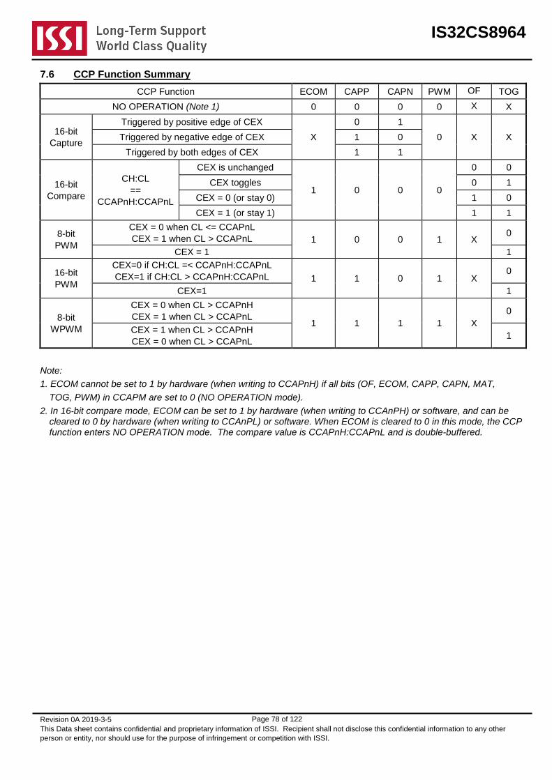
IS32CS8964
Revision 0A 2019-3-5
This Data sheet contains confidential and proprietary information of ISSI. Recipient shall not disclose this confidential information to any other
person or entity, nor should use for the purpose of infringement or competition with ISSI.
Page 78 of 122
7.6 CCP Function Summary
CCP Function ECOM CAPP CAPN PWM OF TOG
NO OPERATION (Note 1) 0 0 0 0 X X
16-bit
Capture
Triggered by positive edge of CEX
X
0 1
0 X X Triggered by negative edge of CEX 1 0
Triggered by both edges of CEX 1 1
16-bit
Compare
CH:CL
==
CCAPnH:CCAPnL
CEX is unchanged
1 0 0 0
0 0
CEX toggles 0 1
CEX = 0 (or stay 0) 1 0
CEX = 1 (or stay 1) 1 1
8-bit
PWM
CEX = 0 when CL <= CCAPnL
CEX = 1 when CL > CCAPnL 1 0 0 1 X 0
CEX = 1 1
16-bit
PWM
CEX=0 if CH:CL =< CCAPnH:CCAPnL
CEX=1 if CH:CL > CCAPnH:CCAPnL 1 1 0 1 X 0
CEX=1 1
8-bit
WPWM
CEX = 0 when CL > CCAPnH
CEX = 1 when CL > CCAPnL 1 1 1 1 X
0
CEX = 1 when CL > CCAPnH
CEX = 0 when CL > CCAPnL 1
Note:
1. ECOM cannot be set to 1 by hardware (when writing to CCAPnH) if all bits (OF, ECOM, CAPP, CAPN, MAT,
TOG, PWM) in CCAPM are set to 0 (NO OPERATION mode).
2. In 16-bit compare mode, ECOM can be set to 1 by hardware (when writing to CCAnPH) or software, and can be cleared to 0 by hardware (when writing to CCAnPL) or software. When ECOM is cleared to 0 in this mode, the CCP function enters NO OPERATION mode. The compare value is CCAPnH:CCAPnL and is double-buffered.

IS32CS8964
Revision 0A 2019-3-5
This Data sheet contains confidential and proprietary information of ISSI. Recipient shall not disclose this confidential information to any other
person or entity, nor should use for the purpose of infringement or competition with ISSI.
Page 79 of 122
8. 16-Bit PWM Controller (PWM16)
This PWM controller provides high precision up to 16-bit Pulse-Width Modulation output with programmable PWM base frequency. The PWM is center-based PWM. There are three channels complementary PWM output with dead time control. The block diagram of PWM control is shown in the following block diagram.
3-BIT
CLOCK SCALING
15-BIT
U/D COUNTER
PWMPRD[15-0]PWMA[14-0]
DB
COMPARE
>=
PWMCLK PWMA
DEADTIME
DEADTIME
PWMAP
PWMAN
PWM CHANNEL A
PWM CHANNEL B
PWMBP
PWMBN
PWM CHANNEL C
PWMCP
PWMCN
PWMCNT[15-0]
PWMTG0[15-0] DB
=
PWMCNT[15-0]
PWMTG1[15-0] DB
=
PWMCNT[15-0]
ADC TRIGGER
ADC TRIGGER
SYSCLK
XOR
PPOL
XOR
NPOL
EMG
EMG
PEMG
NEMG
The period of the PWM frequency is defined by PWNPRD[14-0]. PWMPRD[15] is the enable control of the PWM and when read it represents up/down direction. A 15-bit Up/Down counter is used to provide the time base of the PWM channels. The operation of the PWM waveform is illustrated in the following timing diagram.
PWMPRD[14-0]
PWMCNT[15]=0 PWMCNT[15]=1
PWMA[14-0]
PWMA
PWMAP
PWMA
PWMAN
DT
DT
There are additional two trigger setting PWMTG0[15-0] and PWMTG1[15-0]. The setting allows arbitrary setting of interrupt and ADC conversion triggers. All register are double buffered except PWMPRD and the buffer is updated when PWMCNT=0. The dead time is applied only to the 0 to 1 transition of the PWM outputs such as PWMAP and PWMAN as indicated in the timing diagram. The dead time is specified in SYSCLK period (not PWMCLK period). The following registers are used in PWM configurations and setting.
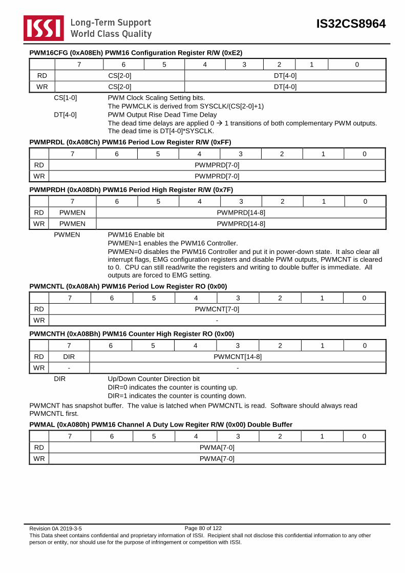
IS32CS8964
Revision 0A 2019-3-5
This Data sheet contains confidential and proprietary information of ISSI. Recipient shall not disclose this confidential information to any other
person or entity, nor should use for the purpose of infringement or competition with ISSI.
Page 80 of 122
PWM16CFG (0xA08Eh) PWM16 Configuration Register R/W (0xE2)
7 6 5 4 3 2 1 0
RD CS[2-0] DT[4-0]
WR CS[2-0] DT[4-0]
CS[1-0] PWM Clock Scaling Setting bits.
The PWMCLK is derived from SYSCLK/(CS[2-0]+1)
DT[4-0] PWM Output Rise Dead Time Delay
The dead time delays are applied 0 1 transitions of both complementary PWM outputs. The dead time is DT[4-0]*SYSCLK.
PWMPRDL (0xA08Ch) PWM16 Period Low Register R/W (0xFF)
7 6 5 4 3 2 1 0
RD PWMPRD[7-0]
WR PWMPRD[7-0]
PWMPRDH (0xA08Dh) PWM16 Period High Register R/W (0x7F)
7 6 5 4 3 2 1 0
RD PWMEN PWMPRD[14-8]
WR PWMEN PWMPRD[14-8]
PWMEN PWM16 Enable bit
PWMEN=1 enables the PWM16 Controller.
PWMEN=0 disables the PWM16 Controller and put it in power-down state. It also clear all interrupt flags, EMG configuration registers and disable PWM outputs, PWMCNT is cleared to 0. CPU can still read/write the registers and writing to double buffer is immediate. All outputs are forced to EMG setting.
PWMCNTL (0xA08Ah) PWM16 Period Low Register RO (0x00)
7 6 5 4 3 2 1 0
RD PWMCNT[7-0]
WR -
PWMCNTH (0xA08Bh) PWM16 Counter High Register RO (0x00)
7 6 5 4 3 2 1 0
RD DIR PWMCNT[14-8]
WR - -
DIR Up/Down Counter Direction bit
DIR=0 indicates the counter is counting up.
DIR=1 indicates the counter is counting down.
PWMCNT has snapshot buffer. The value is latched when PWMCNTL is read. Software should always read PWMCNTL first.
PWMAL (0xA080h) PWM16 Channel A Duty Low Regiter R/W (0x00) Double Buffer
7 6 5 4 3 2 1 0
RD PWMA[7-0]
WR PWMA[7-0]

IS32CS8964
Revision 0A 2019-3-5
This Data sheet contains confidential and proprietary information of ISSI. Recipient shall not disclose this confidential information to any other
person or entity, nor should use for the purpose of infringement or competition with ISSI.
Page 81 of 122
PWMAH (0xA081h) PWM16 Channel A Duty High Register RW (0x00) Double Buffer
7 6 5 4 3 2 1 0
RD - PWMA[14-8]
WR IMM PWMA[14-8]
IMM Immediate Write Control bit
If IMM=1 during write operation, both the high byte and low byte value is written into the holding register and immediately updated into the double buffer.
If IMM=0 during write operation, then the value is written to a holding register, and the compare value is updated under DBS setting.
The read operation always returns the value of the holding register.
PWMBL (0xA082h) PWM16 Channel B Duty Low Regiter R/W (0x00) Double Buffer
7 6 5 4 3 2 1 0
RD PWMB[7-0]
WR PWMB[7-0]
PWMBH (0xA083h) PWM16 Channel B Duty High Register RW (0x00) Double Buffer
7 6 5 4 3 2 1 0
RD - PWMB[14-8]
WR IMM PWMB[14-8]
IMM Immediate Write Control bit
If IMM=1 during write operation, both the high byte and low byte value is written into the holding register and immediately updated into the double buffer.
If IMM=0 during write operation, then the value is written to a holding register, and the compare value is updated under DBS setting.
The read operation always returns the value of the holding register.
PWMCL (0xA084h) PWM16 Channel C Duty Low Regiter R/W (0x00) Double Buffer
7 6 5 4 3 2 1 0
RD PWMC[7-0]
WR PWMC[7-0]
PWMCH (0xA085h) PWM16 Channel C Duty High Register RW (0x00) Double Buffer
7 6 5 4 3 2 1 0
RD - PWMC[14-8]
WR IMM PWMC[14-8]
IMM Immediate Write Control bit
If IMM=1 during write operation, both the high byte and low byte value is written into the holding register and immediately updated into the double buffer.
If IMM=0 during write operation, then the value is written to a holding register, and the compare value is updated under DBS setting.
The read operation always returns the value of the holding register.
The PWM controller can generate interrupts at its count equals to the period or when counting reaches 0. There are two additional trigger settings for generating interrupts or for ADC conversion triggering. These are configured by PWM16INT register.
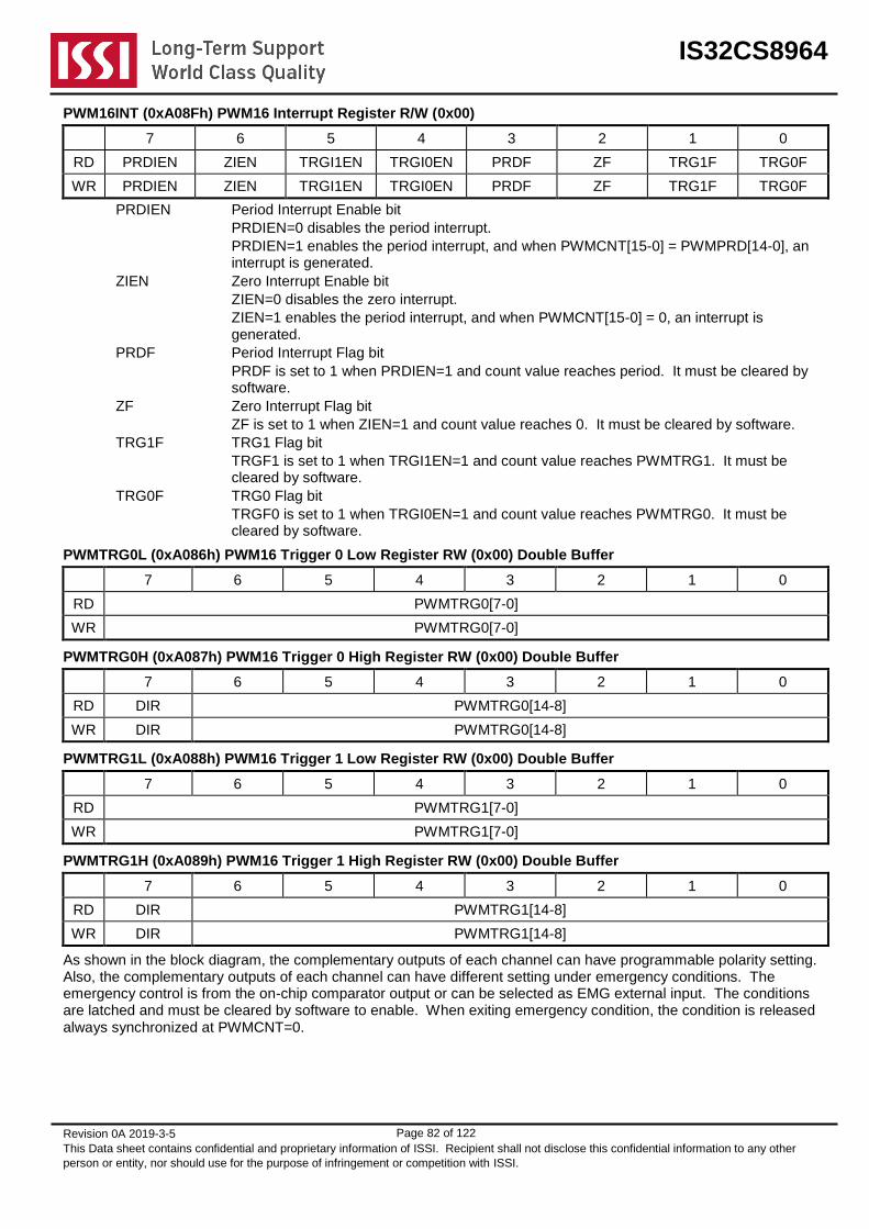
IS32CS8964
Revision 0A 2019-3-5
This Data sheet contains confidential and proprietary information of ISSI. Recipient shall not disclose this confidential information to any other
person or entity, nor should use for the purpose of infringement or competition with ISSI.
Page 82 of 122
PWM16INT (0xA08Fh) PWM16 Interrupt Register R/W (0x00)
7 6 5 4 3 2 1 0
RD PRDIEN ZIEN TRGI1EN TRGI0EN PRDF ZF TRG1F TRG0F
WR PRDIEN ZIEN TRGI1EN TRGI0EN PRDF ZF TRG1F TRG0F
PRDIEN Period Interrupt Enable bit
PRDIEN=0 disables the period interrupt.
PRDIEN=1 enables the period interrupt, and when PWMCNT[15-0] = PWMPRD[14-0], an interrupt is generated.
ZIEN Zero Interrupt Enable bit
ZIEN=0 disables the zero interrupt.
ZIEN=1 enables the period interrupt, and when PWMCNT[15-0] = 0, an interrupt is generated.
PRDF Period Interrupt Flag bit
PRDF is set to 1 when PRDIEN=1 and count value reaches period. It must be cleared by software.
ZF Zero Interrupt Flag bit
ZF is set to 1 when ZIEN=1 and count value reaches 0. It must be cleared by software.
TRG1F TRG1 Flag bit
TRGF1 is set to 1 when TRGI1EN=1 and count value reaches PWMTRG1. It must be cleared by software.
TRG0F TRG0 Flag bit
TRGF0 is set to 1 when TRGI0EN=1 and count value reaches PWMTRG0. It must be cleared by software.
PWMTRG0L (0xA086h) PWM16 Trigger 0 Low Register RW (0x00) Double Buffer
7 6 5 4 3 2 1 0
RD PWMTRG0[7-0]
WR PWMTRG0[7-0]
PWMTRG0H (0xA087h) PWM16 Trigger 0 High Register RW (0x00) Double Buffer
7 6 5 4 3 2 1 0
RD DIR PWMTRG0[14-8]
WR DIR PWMTRG0[14-8]
PWMTRG1L (0xA088h) PWM16 Trigger 1 Low Register RW (0x00) Double Buffer
7 6 5 4 3 2 1 0
RD PWMTRG1[7-0]
WR PWMTRG1[7-0]
PWMTRG1H (0xA089h) PWM16 Trigger 1 High Register RW (0x00) Double Buffer
7 6 5 4 3 2 1 0
RD DIR PWMTRG1[14-8]
WR DIR PWMTRG1[14-8]
As shown in the block diagram, the complementary outputs of each channel can have programmable polarity setting. Also, the complementary outputs of each channel can have different setting under emergency conditions. The emergency control is from the on-chip comparator output or can be selected as EMG external input. The conditions are latched and must be cleared by software to enable. When exiting emergency condition, the condition is released always synchronized at PWMCNT=0.

IS32CS8964
Revision 0A 2019-3-5
This Data sheet contains confidential and proprietary information of ISSI. Recipient shall not disclose this confidential information to any other
person or entity, nor should use for the purpose of infringement or competition with ISSI.
Page 83 of 122
PWM16CHS (0xA09Fh) PWM16 PN Channel Setting Register R/W (0x00)
7 6 5 4 3 2 1 0
RD NEMG[1-0] PEMG[1-0] EMGF[1-0] NPOL PPOL
WR NEMG[1-0] PEMG[1-0] EMGF[1-0] NPOL PPOL
NEMG[1-0] N Channel Emergency State Setting
This setting determines the output states to be forced during emergency condition and applies to A, B and C channels.
NEMG[1-0] = 00, N outputs are forced to Hi-Z
NEMG[1-0] = 01, N outputs are forced to Hi-Z
NEMG[1-0] = 10, N outputs are forced to 0
NEMG[1-0] = 11, N outputs are forced to 1
PEMG[1-0] P Channel Emergency State Setting
This setting determines the output states to be forced during emergency condition and applies to A, B and C channels.
PEMG[1-0] = 00, P outputs are forced to Hi-Z
PEMG[1-0] = 01, P outputs are forced to Hi-Z
PEMG[1-0] = 10, P outputs are forced to 0
PEMG[1-0] = 11, P outputs are forced to 1
EMGF[1-0] Emergency Condition Noise Filter
This setting defines the noise filters on emergency conditions meaning the minimum duration emergency conditions must elapse and hold valid to assert. This applies to external EMG input and the comparator inputs.
EMGF[1-0] = 00, no filter. The P/N channel outputs will be influenced by the XEMG inputs directly while PWNEN=1. Please make sure both the IO Buffer Configuration Registers and the Multi-function Configuration Registers were readied before enable the PWM controller.
EMGF[1-0] = 01, 1 system clock period.
EMGF[1-0] = 10, 2 system clock period.
EMGF[1-0] = 11, 3 system clock period.
NPOL N Channel Output Polarity
NPOL setting controls the N channels output polarity and applies to A, B, and C channels
NPOL=0, no inversion.
NPOL=1, inversion.
PPOL P Channel Output Polarity
PPOL setting controls the P channels output polarity and applies to A, B, and C channels
PPOL=0, no inversion.
PPOL=1, inversion.
PWM16EMG (0xA097h) PWM16 EMG Configuration Register R/W (0x00)
7 6 5 4 3 2 1 0
RD EMGEN LATEN - XEMGF CMPAF CMPBF CMPCF CMPDF
WR EMGEN LATEN - XEMGEN CMPAEN CMPBEN CMPCEN CMPDEN
All EMG Configuration Registers and EMG flags will be cleared to 0x00 if PWM is disabled. So the PWMEN shall be enabled before programming these configuration registers. Users can gate the PWM outputs by setting IO Buffer Configuration Registers and the Multi-function Configuration Registers to avoid unexpected PWM waveforms before finish EMG configuring.
EMGEN Emergency Function Enable bit
EMGEN=0 disable the Emergency control function of PWM output.
EMGEN=1 allows the internal comparator output and an external input as emergency control. When an emergency occurs, both complementary PWM channel outputs are forced to 0.
LATEN Condition Latch Enable bit
LATEN=0 treat these emergency conditions as real-time signals and disables the output only when the signals are valid.

IS32CS8964
Revision 0A 2019-3-5
This Data sheet contains confidential and proprietary information of ISSI. Recipient shall not disclose this confidential information to any other
person or entity, nor should use for the purpose of infringement or competition with ISSI.
Page 84 of 122
LATEN=1 treat these emergency conditions as triggering signals and will latch the conditions. The emergency condition persists until all the flags are cleared by software.
XEMGEN External EMG Input Enable bit
XENGEN=0 disables the external EMG input
XEMGEN=1 enables the external EMG input function.
XEMGF External EMG Flag bit
XEMGF reflects the external EMG input status if LATEN=0. If LATEN=1, it is the latched status of external EMG input and set by hardware. To clear the latched status, software must set XEMGEN=0. And then enable it again if desired.
CMPAEN Comparator A as EMG Input Enable bit
CMPAEN=0 disables the internal comparator A output as EMG condition
CMPAEN=1 enables the internal comparator A output as EMG condition
CMPAF Comparator A EMG flag bit
CMPAF reflects the comparator A output status if LATEN=0. If LATEN=1, it is the latched status of comparator A output and set by hardware. To clear the latched status, software must set CMPAEN=0. And then enable it again if desired.
CMPBEN Comparator B as EMG Input Enable bit
CMPBEN=0 disables the internal comparator B output as EMG condition
CMPBEN=1 enables the internal comparator B output as EMG condition
CMPBF Comparator B EMG flag bit
CMPBF reflects the comparator B output status if LATEN=0. If LATEN=1, it is the latched status of comparator B output and set by hardware. To clear the latched status, software must set CMPBEN=0. And then enable it again if desired.
CMPCEN Comparator C as EMG Input Enable bit
CMPCEN=0 disables the internal comparator C output as EMG condition
CMPCEN=1 enables the internal comparator C output as EMG condition
CMPCF Comparator C EMG flag bit
CMPCF reflects the comparator C output status if LATEN=0. If LATEN=1, it is the latched status of comparator C output and set by hardware. To clear the latched status, software must set CMPCEN=0. And then enable it again if desired.
CMPDEN Comparator D as EMG Input Enable bit
CMPDEN=0 disables the internal comparator D output as EMG condition
CMPDEN=1 enables the internal comparator D output as EMG condition
CMPDF Comparator DEMG flag bit
CMPDF reflects the comparator D output status if LATEN=0. If LATEN=1, it is the latched status of comparator D output and set by hardware. To clear the latched status, software must set CMPDEN=0. And then enable it again if desired.
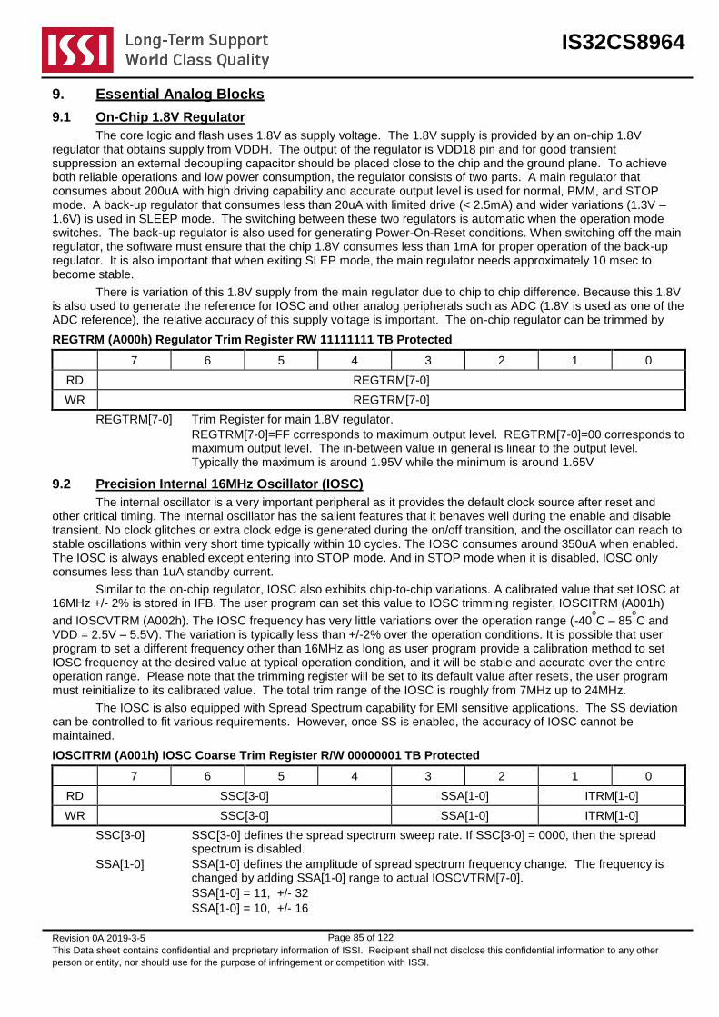
IS32CS8964
Revision 0A 2019-3-5
This Data sheet contains confidential and proprietary information of ISSI. Recipient shall not disclose this confidential information to any other
person or entity, nor should use for the purpose of infringement or competition with ISSI.
Page 85 of 122
9. Essential Analog Blocks
9.1 On-Chip 1.8V Regulator
The core logic and flash uses 1.8V as supply voltage. The 1.8V supply is provided by an on-chip 1.8V regulator that obtains supply from VDDH. The output of the regulator is VDD18 pin and for good transient suppression an external decoupling capacitor should be placed close to the chip and the ground plane. To achieve both reliable operations and low power consumption, the regulator consists of two parts. A main regulator that consumes about 200uA with high driving capability and accurate output level is used for normal, PMM, and STOP mode. A back-up regulator that consumes less than 20uA with limited drive (< 2.5mA) and wider variations (1.3V – 1.6V) is used in SLEEP mode. The switching between these two regulators is automatic when the operation mode switches. The back-up regulator is also used for generating Power-On-Reset conditions. When switching off the main regulator, the software must ensure that the chip 1.8V consumes less than 1mA for proper operation of the back-up regulator. It is also important that when exiting SLEP mode, the main regulator needs approximately 10 msec to become stable.
There is variation of this 1.8V supply from the main regulator due to chip to chip difference. Because this 1.8V is also used to generate the reference for IOSC and other analog peripherals such as ADC (1.8V is used as one of the ADC reference), the relative accuracy of this supply voltage is important. The on-chip regulator can be trimmed by
REGTRM (A000h) Regulator Trim Register RW 11111111 TB Protected
7 6 5 4 3 2 1 0
RD REGTRM[7-0]
WR REGTRM[7-0]
REGTRM[7-0] Trim Register for main 1.8V regulator.
REGTRM[7-0]=FF corresponds to maximum output level. REGTRM[7-0]=00 corresponds to maximum output level. The in-between value in general is linear to the output level. Typically the maximum is around 1.95V while the minimum is around 1.65V
9.2 Precision Internal 16MHz Oscillator (IOSC)
The internal oscillator is a very important peripheral as it provides the default clock source after reset and other critical timing. The internal oscillator has the salient features that it behaves well during the enable and disable transient. No clock glitches or extra clock edge is generated during the on/off transition, and the oscillator can reach to stable oscillations within very short time typically within 10 cycles. The IOSC consumes around 350uA when enabled. The IOSC is always enabled except entering into STOP mode. And in STOP mode when it is disabled, IOSC only consumes less than 1uA standby current.
Similar to the on-chip regulator, IOSC also exhibits chip-to-chip variations. A calibrated value that set IOSC at 16MHz +/- 2% is stored in IFB. The user program can set this value to IOSC trimming register, IOSCITRM (A001h)
and IOSCVTRM (A002h). The IOSC frequency has very little variations over the operation range (-40o
C – 85o
C and VDD = 2.5V – 5.5V). The variation is typically less than +/-2% over the operation conditions. It is possible that user program to set a different frequency other than 16MHz as long as user program provide a calibration method to set IOSC frequency at the desired value at typical operation condition, and it will be stable and accurate over the entire operation range. Please note that the trimming register will be set to its default value after resets, the user program must reinitialize to its calibrated value. The total trim range of the IOSC is roughly from 7MHz up to 24MHz.
The IOSC is also equipped with Spread Spectrum capability for EMI sensitive applications. The SS deviation can be controlled to fit various requirements. However, once SS is enabled, the accuracy of IOSC cannot be maintained.
IOSCITRM (A001h) IOSC Coarse Trim Register R/W 00000001 TB Protected
7 6 5 4 3 2 1 0
RD SSC[3-0] SSA[1-0] ITRM[1-0]
WR SSC[3-0] SSA[1-0] ITRM[1-0]
SSC[3-0] SSC[3-0] defines the spread spectrum sweep rate. If SSC[3-0] = 0000, then the spread spectrum is disabled.
SSA[1-0] SSA[1-0] defines the amplitude of spread spectrum frequency change. The frequency is changed by adding SSA[1-0] range to actual IOSCVTRM[7-0].
SSA[1-0] = 11, +/- 32
SSA[1-0] = 10, +/- 16

IS32CS8964
Revision 0A 2019-3-5
This Data sheet contains confidential and proprietary information of ISSI. Recipient shall not disclose this confidential information to any other
person or entity, nor should use for the purpose of infringement or competition with ISSI.
Page 86 of 122
SSA[1-0] = 01, +/- 8
SSA[1-0] = 00, +/- 4
ITRM[1-0] ITRM[1-0] is the coarse trimming of the IOSC.
IOSCVTRM (A002h) IOSC Fine Trim Register WO 10001110 TB Protected
7 6 5 4 3 2 1 0
RD IOSCVTRM[7-0]
WR IOSCVTRM[7-0]
This register provides fine trimming of the IOSC frequency. The higher the value of IOSCVTRM, the lower the frequency is.
The manufacturer trim value is stored in IFB and is trimmed to 16MHz. The user program provides the freedom to set the IOSC at a preferred frequency as long as the program is able to calibrate the frequency. Once set, the IOSC frequency has accuracy deviation within +/- 2% over the operation conditions. The following lists the range of the typical IOSC frequency for each trimming setting.
ITRM[1-0]=00, Frequency_of_IOSC= 3.2MHz - 4.2MHz - 6.2MHz (VTRM[7-0]= 00 - 80 - FF)
ITRM[1-0]=01, Frequency_of_IOSC= 5.1MHz - 10.2MHz (VTRM[7-0]= 00 - FF)
ITRM[1-0]=10, Frequency_of_IOSC= 9.99MHz -19MHz (VTRM[7-0]= 00 - FF)
ITRM[1-0]=11, Frequency_of_IOSC= 11.9MHz - 22.3MHz (VTRM[7-0]= 00 - FF)
The trimming of the IOSC should use the following procedure to obtain the default setting for 16MHz.
Set ITRM = 01, and
Set VTRM = 00, measure frequency
Set VTRM = FF, measure frequency
Set VTRM = 7F, measure frequency
Use binary search to obtain the closest setting for 16MHz
Note: The frequency versus VTRM setting is monotonic. When VTRM = 00, the frequency is highest, and when VTRM = FF, the frequency is lowest.
A hardware Spread Spectrum can be enabled for the IOSC. This is controlled by SSC[3-0]. When SSC[3-0] = 0, the spread spectrum is disabled, and IOSC functions normally as a fixed frequency oscillator. If SSC[3-0] is not 0, then Spread Spectrum is enabled and IOSC frequency is swept according to the setting of SSC[3-0] and SSA[1-0]. The spread is achieved by varying the actual VTRM output to the oscillator circuit thus effectively changes the oscillation frequency. The effect of SSC[3-0] and SSA[1-0] is shown in the following graph.
When Spread Spectrum is enabled, the actual controlling output to IOSC is VTRM[7-0] +/- SSA. This is shown in the graph above as the bold curve. The above example shows SSA[1:0] = 01, and the deviation is +/- 8. SSC[3-0] defines the update time in IOSC cycles. Then we can calculate the period of a complete sweep is 4*SSC*(2SSA+1) IOSC cycles, and we can obtain the sweep frequency from this period. When SS is enabled, the frequency of IOSC varies according to time and setting, therefore, the accuracy of IOSC frequency cannot be guaranteed. Please also note that VTRMOUT is VTRM[7-0] +/- SSA but is bounded by 0 and 255. Therefore for a linear non-clipped sweep, VTRM[7-0] needs to be within the range of SSA – 256-SSA, for example, SSA[10] = 01, then SSA is 8. VTRM[7-0] should be in the range from 8 to 248 to prevent the sweep from being clipped. As Spread Spectrum suggests, the total EMI energy is not reduced, but the energy is spread over wider frequency. It is recommended that SS usage should be carefully evaluated and the setting of spread amplitude and the sweep frequency should be chosen carefully for reducing EMI effect.
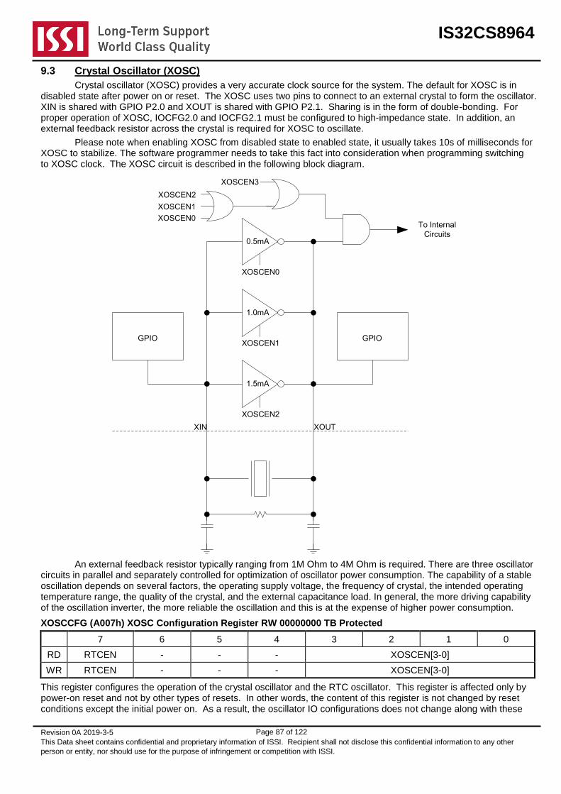
IS32CS8964
Revision 0A 2019-3-5
This Data sheet contains confidential and proprietary information of ISSI. Recipient shall not disclose this confidential information to any other
person or entity, nor should use for the purpose of infringement or competition with ISSI.
Page 87 of 122
9.3 Crystal Oscillator (XOSC)
Crystal oscillator (XOSC) provides a very accurate clock source for the system. The default for XOSC is in disabled state after power on or reset. The XOSC uses two pins to connect to an external crystal to form the oscillator. XIN is shared with GPIO P2.0 and XOUT is shared with GPIO P2.1. Sharing is in the form of double-bonding. For proper operation of XOSC, IOCFG2.0 and IOCFG2.1 must be configured to high-impedance state. In addition, an external feedback resistor across the crystal is required for XOSC to oscillate.
Please note when enabling XOSC from disabled state to enabled state, it usually takes 10s of milliseconds for XOSC to stabilize. The software programmer needs to take this fact into consideration when programming switching to XOSC clock. The XOSC circuit is described in the following block diagram.
XOSCEN0
0.5mA
XOSCEN1
1.0mA
XOSCEN2
1.5mA
GPIOGPIO
XIN XOUT
To Internal
Circuits
XOSCEN0
XOSCEN1
XOSCEN2
XOSCEN3
An external feedback resistor typically ranging from 1M Ohm to 4M Ohm is required. There are three oscillator circuits in parallel and separately controlled for optimization of oscillator power consumption. The capability of a stable oscillation depends on several factors, the operating supply voltage, the frequency of crystal, the intended operating temperature range, the quality of the crystal, and the external capacitance load. In general, the more driving capability of the oscillation inverter, the more reliable the oscillation and this is at the expense of higher power consumption.
XOSCCFG (A007h) XOSC Configuration Register RW 00000000 TB Protected
7 6 5 4 3 2 1 0
RD RTCEN - - - XOSCEN[3-0]
WR RTCEN - - - XOSCEN[3-0]
This register configures the operation of the crystal oscillator and the RTC oscillator. This register is affected only by power-on reset and not by other types of resets. In other words, the content of this register is not changed by reset conditions except the initial power on. As a result, the oscillator IO configurations does not change along with these
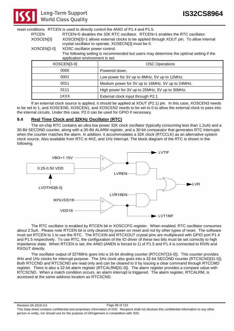
IS32CS8964
Revision 0A 2019-3-5
This Data sheet contains confidential and proprietary information of ISSI. Recipient shall not disclose this confidential information to any other
person or entity, nor should use for the purpose of infringement or competition with ISSI.
Page 88 of 122
reset conditions. RTCEN is used to directly control the ANIO of P1.4 and P1.5.
RTCEN RTCEN=0 disables the 32K RTC oscillator. RTCEN=1 enables the RTC oscillator.
XOSCEN[3] XOSCEN[3]=1 allows external clocks to be applied through XOUT pin. To allow internal crystal oscillator to operate, XOSECN[3] must be 0.
XOSCEN[2-0] XOSC oscillator power control.
The following setting is recommended but users may determine the optimal setting if the application environment is set.
XOSCEN[3-0] OSC Operations
0000 Powered down.
0001 Low power for 3V up to 8MHz, 5V up to 12MHz.
0011 Medium power for 3V up to 16MHz, 5V up to 24MHz.
0111 High power for 3V up to 25MHz, 5V up to 30MHz.
1XXX External clock input through P2.1
If an external clock source is applied, it should be applied at XOUT (P2.1) pin. In this case, XOSCEN3 needs to be set to 1, and XOSCEN0, XOSCEN1, and XOSCEN2 needs to be set to 0 to allow the external clock to pass into the internal circuits. Under this case, P2.0 can be used for GPIO if necessary.
9.4 Real Time Clock and 32KHz Oscillator (RTC)
The on-chip RTC contains an ultra low power 32K clock oscillator (typically consuming less than 1.2uA) and a 30-Bit SECOND counter, along with a 30-Bit ALARM register, and a 30-bit comparator that generates RTC interrupts when the counter matches the alarm. In addition, it accommodates a 32K clock (RTCCLK) as an alternative system clock source. Also available from RTC is 4HZ, and 1Hz interrupt. The block diagram of the RTC is shown in the following.
90%VDD18
LVR18EN
0.25-0.50 VDD
LVDTHD[6-0]
VBG=1.15V
LVTIF
LVR
LVT18IF
LVREN
VDD18
The RTC oscillator is enabled by RTCEN bit in XOSCCFG register. When enabled, RTC oscillator consumes about 2.5uA. Please note RTCEN bit is only cleared by power-on reset and not by other types of reset. The software must set RTCEN to 1 to use the RTC. The RTCXIN and RTCXOUT crystal pins are multiplexed with GPIO port P1.4 and P1.5 respectively. To use RTC, the configuration of the IO driver of these two bits must be set correctly to high impedance state. When RTCEN is set, the ANIO (ANEN is forced to 1) of P1.5 and P1.4 is connected to RXIN and RXOUT directly.
The oscillator output of 32768Hz goes into a 16-bit dividing counter (RTCCNT[15-0]). This counter provides 4Hz and 1Hz clocks for interrupt purpose. The 1Hz clock also goes into a 32-bit SECOND counter (RTCSCND[31-0]). Both RTCCND and RTCSCND are read only and can be cleared to 0 by issuing a clear command through RTCCMD register. There is also a 32-bit alarm register (RTCALRM[31-0]). The alarm register provides a compare value with RTCSCND. When a match condition occurs, an alarm interrupt is triggered. The alarm register, RTCALRM, is accessed at the same address location as RTCSCND.

IS32CS8964
Revision 0A 2019-3-5
This Data sheet contains confidential and proprietary information of ISSI. Recipient shall not disclose this confidential information to any other
person or entity, nor should use for the purpose of infringement or competition with ISSI.
Page 89 of 122
RTCCMD (0xA00E) RTC Configuration and Command Register RW 0000000
7 6 5 4 3 2 1 0
RD SECINTEN ALMINTEN SECINT ALMINT 4HZINTEN 4HZINT CLRSCND CLRCNT
WR SECINTEN ALMINTEN SECINT ALMINT 4HZINTEN 4HZINT CLRSCND CLRCNT
SECINTEN RTC Second Interrupt Enable bit, Set to enable RTC second interrupt. When SECINTEN = 1, RTC generates an interrupt every second.
ALMINTEN Alarm Interrupt Enable bit. Set to enable alarm interrupt.
SECINT Second Interrupt bit. This bit must be cleared by software.
ALMINT Alarm Interrupt bit. This bit must be cleared by software.
4HZINTEN 4Hz Interrupt Enable bit, Set to enable 4Hz interrupt.
4HZINT 4Hz Interrupt bit. Set by hardware every 250 millisecond if enabled. This bit must be cleared by software.
CLRSCND Clear (RTC) Second Counter bit
Set this bit to 1 to force the SECOND counter to 0. CLRSCND must be cleared to 0 to allow the SECOND counter to continue to count.
CLRCNT Clear (RTC) 32K Counter bit
Set this bit to 1 to force the 32768 divider counter to 0. CLRCNT must be cleared to 0 to allow RTC counter to continue to count.
RTCCNTL (0xA00C) RTC Counter Low Byte Register 0 RO 00000000
7 6 5 4 3 2 1 0
RD RTCCNT[7-0]
WR -
This register holds the value for the lower 8 bits of the RTC 32KHz divider counter. The counter value can be cleared by issuing CLRCNT.
RTCCNTH (0xA00D) RTC Counter High Byte Register 1 RO 00000000
7 6 5 4 3 2 1 0
RD RTCCNT[15-8]
WR -
This register holds the value for the upper 8 bits of the RTC 32KHz divider counter. The counter value can be cleared by issuing CLRCNT.
RTCSCND0 (0xA008) RTC SECOND Counter Register 0 RW 00000000
7 6 5 4 3 2 1 0
RD RTCSCND[7-0]
WR RTCALRM[7-0]
This register holds the value for the SECOND counter bit 7 to 0 locations. This is read only and can be cleared by CLRSCND. When written, it writes into the ALARM register.
RTCSCND1 (0xA009) RTC SECOND Counter Register 1 RW 00000000
7 6 5 4 3 2 1 0
RD RTCSCND[15-8]
WR RTCALRM[15-8]
This register holds the value for the SECOND counter bit 15 to 8 locations. This is read only and can be cleared by CLRSCND. When written, it writes into the ALARM register.
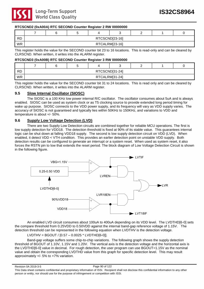
IS32CS8964
Revision 0A 2019-3-5
This Data sheet contains confidential and proprietary information of ISSI. Recipient shall not disclose this confidential information to any other
person or entity, nor should use for the purpose of infringement or competition with ISSI.
Page 90 of 122
RTCSCND2 (0xA00A) RTC SECOND Counter Register 2 RW 00000000
7 6 5 4 3 2 1 0
RD RTCSCND[23-16]
WR RTCALRM[23-16]
This register holds the value for the SECOND counter bit 23 to 16 locations. This is read-only and can be cleared by CLRSCND. When written, it writes into the ALARM register.
RTCSCND3 (0xA00B) RTC SECOND Counter Register 3 RW 00000000
7 6 5 4 3 2 1 0
RD RTCSCND[31-24]
WR RTCALRM[31-24]
This register holds the value for the SECOND counter bit 31 to 24 locations. This is read only and can be cleared by CLRSCND. When written, it writes into the ALARM register.
9.5 Slow Internal Oscillator (SIOSC)
The SIOSC is a 100 KHz low power internal R/C oscillator. The oscillator consumes about 5uA and is always enabled. SIOSC can be used as system clock or as T5 clocking source to provide extended long period timing for wake up purpose. SIOSC connects to the VDD power supply, and its frequency will vary as VDD supply varies. The accuracy of SIOSC is not guaranteed and typically lies within 50KHz to 150KHz, and variations to VDD and temperature is about +/- 50%.
9.6 Supply Low Voltage Detection (LVD)
There are two Supply Low Detection circuits are combined together for reliable MCU operations. The first is low supply detection for VDD18. The detection threshold is fixed at 90% of its stable value. This guarantees internal logic can be shut down at falling VDD18 supply. The second is low supply detection circuit on VDD (LVD). When enabled, it detect VDD < VTH condition. This provides an earlier detection point on unstable VDD supply. Both detection results can be configured to generate an interrupt or a system reset. When used as system reset, it also forces the RSTN pin to low that extends the reset period. The block diagram of Low Voltage Detection Circuit is shown in the following figure.
90%VDD18
LVR18EN
0.25-0.50 VDD
LVDTHD[6-0]
VBG=1.15V
LVTIF
LVR
LVT18IF
LVREN
VDD18
An enabled LVD circuit consumes about 100uA to 400uA depending on its VDD level. The LVDTHD[6-0] sets the compare threshold from 0.25VDD to 0.50VDD against the internal band-gap reference voltage of 1.15V. The detection threshold can be represented in the following equation when LVDTHV is the detection voltage.
LVDTHV = BGOUT / [0.57 – 0.0025 * LVDTHD[6-0]].
Band-gap voltage suffers some chip-to-chip variations. The following graph shows the supply detection threshold of BGOUT of 1.10V, 1.15V and 1.20V. The vertical axis is the detection voltage and the horizontal axis is the LVDTHD[6-0] value in decimal. For rough detection, the user program can use BGOUT=1.15V as the nominal value and obtain the corresponding LVDTHD value from this graph for specific detection level. This may result approximately +/- 5% to +7% variation.

IS32CS8964
Revision 0A 2019-3-5
This Data sheet contains confidential and proprietary information of ISSI. Recipient shall not disclose this confidential information to any other
person or entity, nor should use for the purpose of infringement or competition with ISSI.
Page 91 of 122
For very precise detection level, the manufacturing process stores the LVDTHD value for detection of 4.0V and 3.0V in IFB. The user program can then use these two values and obtain a real average BGOUT value using the above formula. Then use the real BGOUT value to obtain the specific LVDTHD value for an arbitrary detection level.
The user program enables the preferred configuration and sets the appropriate detection threshold level. When enabled, the LVD circuit needs about 10usec to get initialized. The following XFR registers are used for this purpose. Because in the SLEEP mode, the main regulator is turned off and VDD18 is supplied by backup regulator with lower than 1.8V level. LVR18 or LVT18 should be turned off too. This prevents false triggering of the LVR18 or LVT18. These should be turned off before entering SLEEP mode, and enabled after VDD18 is stable after exiting of the SLEEP mode. Typical stable time of VDD18 after the exiting of SLEEP mode is 20usec.
LVDCFG (A010h) Supply Low Voltage Detection Configuration Register RW 10000000 TB Protected
7 6 5 4 3 2 1 0
RD LVDEN LVREN LVTEN LVR18EN LVT18EN - LVT18IF LVTIF
WR LVDEN LVREN LVTEN LVR18EN LVT18EN - LVT18IF LVTIF
LVDEN LVD Enable bit. Set to turn on supply voltage detection circuits.
LVREN LVR Enable bit. LVREN = 1 allows low voltage detect condition to cause a system reset.
LVTEN LVT Enable bit. LVTEN = 1 allows low voltage detect condition to generate an interrupt.
LVR18EN LVR18 Enable bit. LVR18EN = 1 allows low voltage detect condition to cause a system reset.
LVT18EN LVT18 Enable bit. LVT18EN = 1 allows low voltage detect condition to generate an interrupt.
LVT18IF Core VDD18 Low Voltage Detect Interrupt Flag
LVT18IF is set by hardware when LVD detection occurs and must be cleared by software.
LVTIF Low Voltage Detect Interrupt Flag
LVTIF is set by hardware when LVD detection occurs and must be cleared by software.
LVDTHD (A011h) Supply Low Voltage Detection Threshold Register WO XX111111 TB Protected
7 6 5 4 3 2 1 0
RD - LVDTHD6 LVDTHD5 LVDTHD4 LVDTHD3 LVDTHD2 LVDTHD1 LVDTHD0
WR - LVDTHD6 LVDTHD5 LVDTHD4 LVDTHD3 LVDTHD2 LVDTHD1 LVDTHD0
LVDTHD = 00 will set the detection threshold at its minimum (approximately 2.2V), and LVDTHD = 7F will set the detection threshold at its maximum (approximately 4.5V).
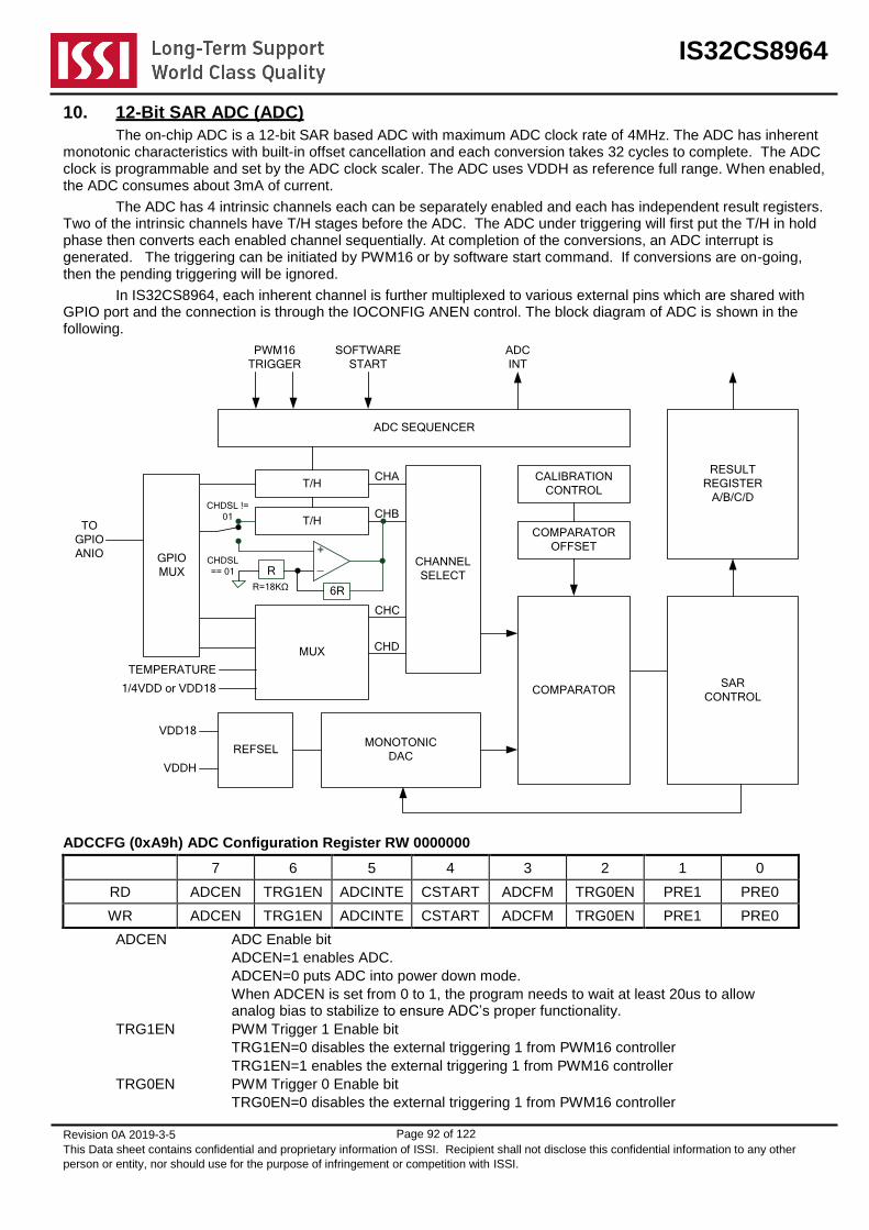
IS32CS8964
Revision 0A 2019-3-5
This Data sheet contains confidential and proprietary information of ISSI. Recipient shall not disclose this confidential information to any other
person or entity, nor should use for the purpose of infringement or competition with ISSI.
Page 92 of 122
10. 12-Bit SAR ADC (ADC)
The on-chip ADC is a 12-bit SAR based ADC with maximum ADC clock rate of 4MHz. The ADC has inherent monotonic characteristics with built-in offset cancellation and each conversion takes 32 cycles to complete. The ADC clock is programmable and set by the ADC clock scaler. The ADC uses VDDH as reference full range. When enabled, the ADC consumes about 3mA of current.
The ADC has 4 intrinsic channels each can be separately enabled and each has independent result registers. Two of the intrinsic channels have T/H stages before the ADC. The ADC under triggering will first put the T/H in hold phase then converts each enabled channel sequentially. At completion of the conversions, an ADC interrupt is generated. The triggering can be initiated by PWM16 or by software start command. If conversions are on-going, then the pending triggering will be ignored.
In IS32CS8964, each inherent channel is further multiplexed to various external pins which are shared with GPIO port and the connection is through the IOCONFIG ANEN control. The block diagram of ADC is shown in the following.
MONOTONIC
DAC
COMPARATOR
COMPARATOR
OFFSET
SAR
CONTROL
ADC SEQUENCER
CHANNEL
SELECT
T/H
T/H
TEMPERATURE
1/4VDD or VDD18
REFSEL
VDD18
VDDH
CALIBRATION
CONTROL
PWM16
TRIGGER
SOFTWARE
START
ADC
INT
RESULT
REGISTER
A/B/C/D
MUX
GPIO
MUX
CHA
CHB
CHC
CHD
TO
GPIO
ANIO
R
6RR=18KΩ
+
_
CHDSL !=
01
CHDSL
== 01
ADCCFG (0xA9h) ADC Configuration Register RW 0000000
7 6 5 4 3 2 1 0
RD ADCEN TRG1EN ADCINTE CSTART ADCFM TRG0EN PRE1 PRE0
WR ADCEN TRG1EN ADCINTE CSTART ADCFM TRG0EN PRE1 PRE0
ADCEN ADC Enable bit
ADCEN=1 enables ADC.
ADCEN=0 puts ADC into power down mode.
When ADCEN is set from 0 to 1, the program needs to wait at least 20us to allow analog bias to stabilize to ensure ADC’s proper functionality.
TRG1EN PWM Trigger 1 Enable bit
TRG1EN=0 disables the external triggering 1 from PWM16 controller
TRG1EN=1 enables the external triggering 1 from PWM16 controller
TRG0EN PWM Trigger 0 Enable bit
TRG0EN=0 disables the external triggering 1 from PWM16 controller
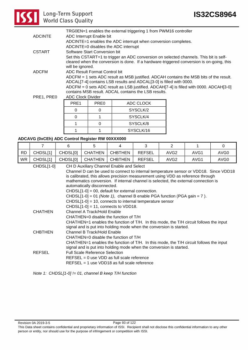
IS32CS8964
Revision 0A 2019-3-5
This Data sheet contains confidential and proprietary information of ISSI. Recipient shall not disclose this confidential information to any other
person or entity, nor should use for the purpose of infringement or competition with ISSI.
Page 93 of 122
TRG0EN=1 enables the external triggering 1 from PWM16 controller
ADCINTE ADC Interrupt Enable bit
ADCINTE=1 enables the ADC interrupt when conversion completes.
ADCINTE=0 disables the ADC interrupt
CSTART Software Start Conversion bit
Set this CSTART=1 to trigger an ADC conversion on selected channels. This bit is self-cleared when the conversion is done. If a hardware-triggered conversion is on-going, this will be ignored.
ADCFM ADC Result Format Control bit
ADCFM = 1 sets ADC result as MSB justified. ADCAH contains the MSB bits of the result. ADCAL[7-4] contains LSB results and ADCAL[3-0] is filled with 0000.
ADCFM = 0 sets ADC result as LSB justified. ADCAH[7-4] is filled with 0000. ADCAH[3-0] contains MSB result. ADCAL contains the LSB results.
PRE1, PRE0 ADC Clock Divider
PRE1 PRE0 ADC CLOCK
0 0 SYSCLK/2
0 1 SYSCLK/4
1 0 SYSCLK/8
1 1 SYSCLK/16
ADCAVG (0xCEh) ADC Control Register RW 00XXX000
7 6 5 4 3 2 1 0
RD CHDSL[1] CHDSL[0] CHATHEN CHBTHEN REFSEL AVG2 AVG1 AVG0
WR CHDSL[1] CHDSL[0] CHATHEN CHBTHEN REFSEL AVG2 AVG1 AVG0
CHDSL[1-0] CH D Auxiliary Channel Enable and Select
Channel D can be used to connect to internal temperature sensor or VDD18. Since VDD18 is calibrated, this allows precision measurement using VDD as reference through mathematics conversion. If internal channel is selected, the external connection is automatically disconnected.
CHDSL[1-0] = 00, default for external connection.
CHDSL[1-0] = 01 (Note 1), channel B enable PGA function (PGA gain = 7 ).
CHDSL[1-0] = 10, connects to internal temperature sensor
CHDSL[1-0] = 11, connects to VDD18.
CHATHEN Channel A Track/Hold Enable
CHATHEN=0 disable the function of T/H
CHATHEN=1 enables the function of T/H. In this mode, the T/H circuit follows the input signal and is put into holding mode when the conversion is started.
CHBTHEN Channel B Track/Hold Enable
CHATHEN=0 disable the function of T/H
CHATHEN=1 enables the function of T/H. In this mode, the T/H circuit follows the input signal and is put into holding mode when the conversion is started.
REFSEL Full Scale Reference Selection
REFSEL = 0 use VDD as full scale reference
REFSEL = 1 use VDD18 as full scale reference
Note 1: CHDSL[1-0] != 01, channel B keep T/H function

IS32CS8964
Revision 0A 2019-3-5
This Data sheet contains confidential and proprietary information of ISSI. Recipient shall not disclose this confidential information to any other
person or entity, nor should use for the purpose of infringement or competition with ISSI.
Page 94 of 122
AVG[2-0] AVG[2-0] controls the hardware averaging logic of ADC readout. It is recommended the
setting is changed only when ADC is stopped. If multiple channels are enabled, then each channel is averaged in sequence. The default is 000.
AVG2 AVG1 AVG0 ADC Result
0 0 0 1 Times Average
0 0 1 2 Times Average
0 1 0 4 Times Average
0 1 1 8 Times Average
1 0 0 16 Times Average
1 0 1 32 Times Average
1 1 0 64 Times Average
1 1 1 TEST MODE
ADCCHSL (0xB9h) ADC Channel Selection and Interrupt Status RW 0000XXXX
7 6 5 4 3 2 1 0
RD ADCCHA ADCCHB ADCCHC ADCCHD CHAIF CHBIF CHCIF CHDIF
WR ADCCHA ADCCHB ADCCHC ADCCHD - - - -
ADCCHA ADCCHA=1 enables ADC Channel A for conversion cycle
ADCCHB ADCCHB=1 enables ADC Channel B for conversion cycle
ADCCHC ADCCHC=1 enables ADC Channel C for conversion cycle
ADCCHD ADCCHD=1 enables ADC Channel D for conversion cycle
CHAIF Channel A Conversion Completion Interrupt Flag bit
CHAIF is set by hardware when the conversion is completed and new result is written to ADCAL and ADCAH result registers. If ADC interrupt is enabled, this also generates an interrupt. This bit is cleared when ADCAL is read. When this flag is set, no new conversion result is updated.
CHBIF Channel B Conversion Completion Interrupt Flag bit
CHBIF is set by hardware when the conversion is completed and new result is written to ADCBL and ADCBH result registers. If ADC interrupt is enabled, this also generates an interrupt. This bit is cleared when ADCBL is read. When this flag is set, no new conversion result is updated.
CHCIF Channel C Conversion Completion Interrupt Flag bit
CHCIF is set by hardware when the conversion is completed and new result is written to ADCCL and ADCCH result registers. If ADC interrupt is enabled, this also generates an interrupt. This bit is cleared when ADCCL is read. When this flag is set, no new conversion result is updated.
CHDIF Channel D Conversion Completion Interrupt Flag bit
CHDIF is set by hardware when the conversion is completed and new result is written to ADCDL and ADCDH result registers. If ADC interrupt is enabled, this also generates an interrupt. This bit is cleared when ADCDL is read. When this flag is set, no new conversion result is updated.
ADCAH to ADCDH and ADCAL to ADCDL are the low and high byte result registers respectively, and are read-only. Reading low byte result also clears its corresponding interrupt flag. If the flag is not cleared, no new result is updated. The software should always read the low byte last. The format of the high byte and low byte depends on ADCFM setting.
ADCAL (0xBAh) Channel A Result Register Low Byte RW XXXXXXXX
7 6 5 4 3 2 1 0
RD CH A Result
WR -

IS32CS8964
Revision 0A 2019-3-5
This Data sheet contains confidential and proprietary information of ISSI. Recipient shall not disclose this confidential information to any other
person or entity, nor should use for the purpose of infringement or competition with ISSI.
Page 95 of 122
ADCAH (0xBBh) Channel A Result Register High Byte RW XXXXXXXX
7 6 5 4 3 2 1 0
RD CH A Result
WR -
ADCBL (0xBCh) Channel B Result Register Low Byte RW XXXXXXXX
7 6 5 4 3 2 1 0
RD CH B Result
WR -
ADCBH (0xBDh) Channel B Result Register High Byte RW XXXXXXXX
7 6 5 4 3 2 1 0
RD CH B Result
WR -
ADCCL (0xBEh) Channel C Result Register Low Byte RO XXXXXXXX
7 6 5 4 3 2 1 0
RD CH C Result
WR -
ADCCH (0xBFh) Channel C Result Register High Byte RW XXXXXXXX
7 6 5 4 3 2 1 0
RD CH C Result
WR -
ADCDL (0xAAh) Channel D Result Register Low Byte RO XXXXXXXX
7 6 5 4 3 2 1 0
RD CH D Result
WR -
ADCDH (0xABh) Channel D Result Register High Byte RO XXXXXXXX
7 6 5 4 3 2 1 0
RD CH D Result
WR -

IS32CS8964
Revision 0A 2019-3-5
This Data sheet contains confidential and proprietary information of ISSI. Recipient shall not disclose this confidential information to any other
person or entity, nor should use for the purpose of infringement or competition with ISSI.
Page 96 of 122
11. Analog Comparators (ACMP)
IS32CS8964 has four analog comparators as its on-chip external peripherals. When enabled, each comparator consumes about 250uA. The input signal range is from 0 to VDD. There are two 8-bit R-2R DAC associated with the comparators to generate the compare threshold. The R-2R DAC uses the internal 1.8V supply as the full scale range thus limiting the comparator threshold from 0V to 1.8V in 256 steps. Channel B/C/D can select a common external threshold. The inputs of the comparators are multiplexed with multi-function GPIO pins, P2.7/P3.3, P2.6, P2.5, P2.4 and the external threshold is through P2.3. To use these ports as comparator inputs, the ANEN must be enabled and other drivers to be in high-impedance state.
The real-time outputs of the comparator can be read by the CPU directly through register access. The output is also sent to an edge-detector and any edge transition can be used to trigger an interrupt. The stabilization time from off state to enabled state of the comparator block is about 20usec. The block diagram of the analog comparator is shown in the following diagram.
MU
X EDGE
DETECTCMPA INT
CMPSTAVT
H0
VT
H1
CMPA
EN
MU
X EDGE
DETECTCMPB INT
CMPSTB
CMPB
EN
MU
X EDGE
DETECTCMPC INT
CMPSTC
CMPC
EN
MU
X EDGE
DETECTCMPD INT
CMPSTD
CMPD
EN
DAC
0 – VDD18
CMPTH
CMPTH0[7-0]
CMPTH1[7-0]
POLA
POLB
POLC
POLD
CMPCFGAB (0xA030h) Analog Comparator A/B Configuration Register RW 0000000
7 6 5 4 3 2 1 0
RD CMPENA THSELA INTENA POLA CMPENB THSELB INTENB POLB
WR CMPENA THSELA INTENA POLA CMPENB THSELB INTENB POLB
CMPENA Comparator A Enable bit. Set to enable the comparator.
When CMPENA is set from 0 to 1, the program needs to wait at least 20us allowing analog bias to stabilize to ensure comparator A’s proper functionality.
THSELA Comparator A Threshold Select bit. THSELA = 0, the comparator A uses VTH0 as the threshold. THSELA = 1, the comparator A uses VTH1 as the threshold.
INTENA Set to enable the comparator A interrupt.
POLA Channel A Output polarity control bit
POLA=0 set default polarity
POLA=1 reverse the output polarity of the comparator
CMPENB Comparator B Enable bit. Set to enable the comparator.
When CMPENB is set from 0 to 1, the program needs to wait at least 20us allowing analog bias to stabilize to ensure comparator B’s proper functionality.
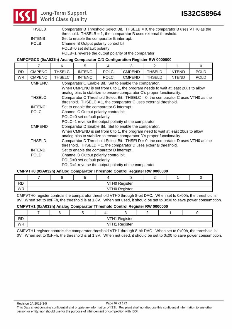
IS32CS8964
Revision 0A 2019-3-5
This Data sheet contains confidential and proprietary information of ISSI. Recipient shall not disclose this confidential information to any other
person or entity, nor should use for the purpose of infringement or competition with ISSI.
Page 97 of 122
THSELB Comparator B Threshold Select Bit. THSELB = 0, the comparator B uses VTH0 as the threshold. THSELB = 1, the comparator B uses external threshold.
INTENB Set to enable the comparator B interrupt.
POLB Channel B Output polarity control bit
POLB=0 set default polarity
POLB=1 reverse the output polarity of the comparator
CMPCFGCD (0xA031h) Analog Comparator C/D Configuration Register RW 0000000
7 6 5 4 3 2 1 0
RD CMPENC THSELC INTENC POLC CMPEND THSELD INTEND POLD
WR CMPENC THSELC INTENC POLC CMPEND THSELD INTEND POLD
CMPENC Comparator C Enable Bit. Set to enable the comparator.
When CMPENC is set from 0 to 1, the program needs to wait at least 20us to allow analog bias to stabilize to ensure comparator C’s proper functionality.
THSELC Comparator C Threshold Select Bit. THSELC = 0, the comparator C uses VTH0 as the threshold. THSELC = 1, the comparator C uses external threshold.
INTENC Set to enable the comparator C interrupt.
POLC Channel C Output polarity control bit
POLC=0 set default polarity
POLC=1 reverse the output polarity of the comparator
CMPEND Comparator D Enable Bit. Set to enable the comparator.
When CMPEND is set from 0 to 1, the program need to wait at least 20us to allow analog bias to stabilize to ensure comparator D’s proper functionality.
THSELD Comparator D Threshold Select Bit. THSELD = 0, the comparator D uses VTH0 as the threshold. THSELD = 1, the comparator D uses external threshold.
INTEND Set to enable the comparator D interrupt.
POLD Channel D Output polarity control bit
POLD=0 set default polarity
POLD=1 reverse the output polarity of the comparator
CMPVTH0 (0xA032h) Analog Comparator Threshold Control Register RW 0000000
7 6 5 4 3 2 1 0
RD VTH0 Register
WR VTH0 Register
CMPVTH0 register controls the comparator threshold VTH0 through 8-bit DAC. When set to 0x00h, the threshold is 0V. When set to 0xFFh, the threshold is at 1.8V. When not used, it should be set to 0x00 to save power consumption.
CMPVTH1 (0xA033h) Analog Comparator Threshold Control Register RW 0000000
7 6 5 4 3 2 1 0
RD VTH1 Register
WR VTH1 Register
CMPVTH1 register controls the comparator threshold VTH1 through 8-bit DAC. When set to 0x00h, the threshold is 0V. When set to 0xFFh, the threshold is at 1.8V. When not used, it should be set to 0x00 to save power consumption.
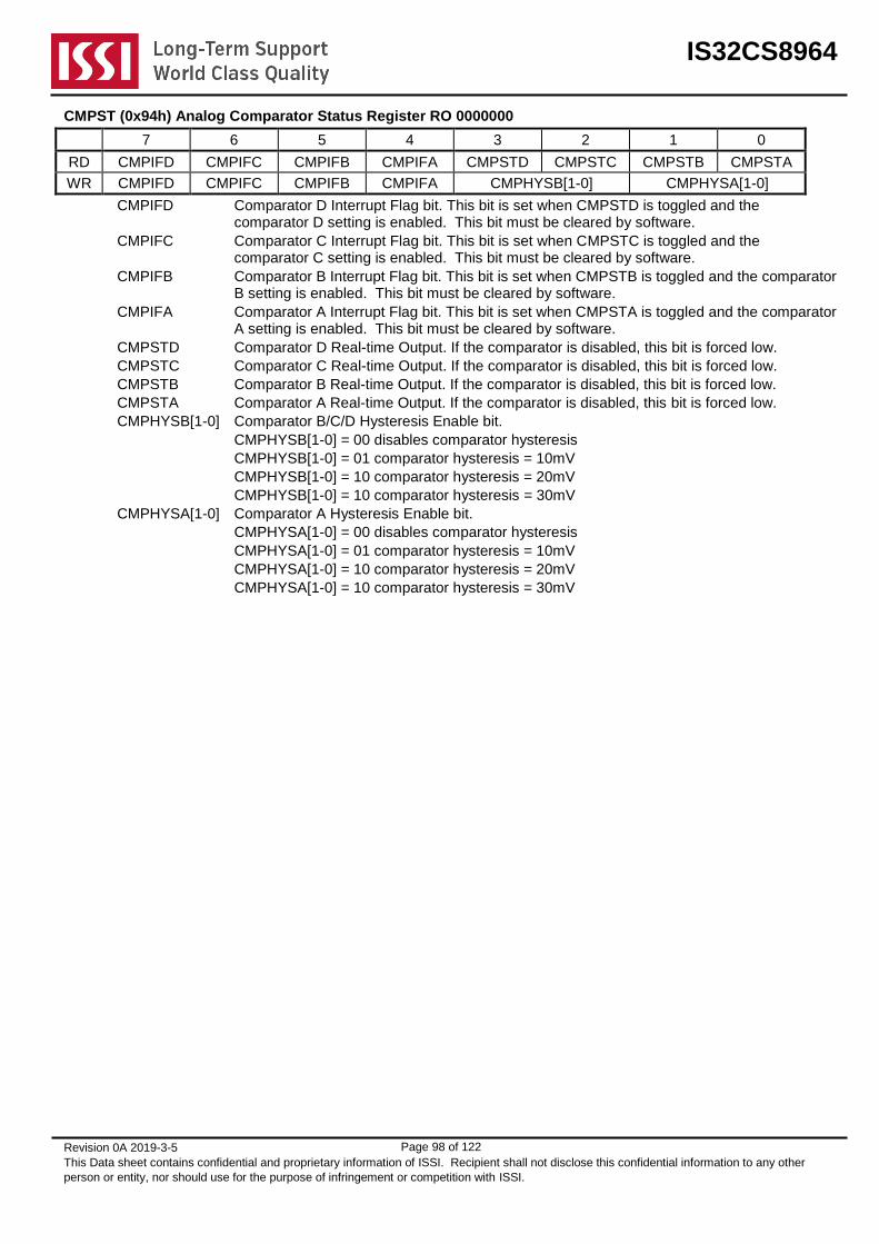
IS32CS8964
Revision 0A 2019-3-5
This Data sheet contains confidential and proprietary information of ISSI. Recipient shall not disclose this confidential information to any other
person or entity, nor should use for the purpose of infringement or competition with ISSI.
Page 98 of 122
CMPST (0x94h) Analog Comparator Status Register RO 0000000
7 6 5 4 3 2 1 0
RD CMPIFD CMPIFC CMPIFB CMPIFA CMPSTD CMPSTC CMPSTB CMPSTA
WR CMPIFD CMPIFC CMPIFB CMPIFA CMPHYSB[1-0] CMPHYSA[1-0]
CMPIFD Comparator D Interrupt Flag bit. This bit is set when CMPSTD is toggled and the comparator D setting is enabled. This bit must be cleared by software.
CMPIFC Comparator C Interrupt Flag bit. This bit is set when CMPSTC is toggled and the comparator C setting is enabled. This bit must be cleared by software.
CMPIFB Comparator B Interrupt Flag bit. This bit is set when CMPSTB is toggled and the comparator B setting is enabled. This bit must be cleared by software.
CMPIFA Comparator A Interrupt Flag bit. This bit is set when CMPSTA is toggled and the comparator A setting is enabled. This bit must be cleared by software.
CMPSTD Comparator D Real-time Output. If the comparator is disabled, this bit is forced low.
CMPSTC Comparator C Real-time Output. If the comparator is disabled, this bit is forced low.
CMPSTB Comparator B Real-time Output. If the comparator is disabled, this bit is forced low.
CMPSTA Comparator A Real-time Output. If the comparator is disabled, this bit is forced low.
CMPHYSB[1-0] Comparator B/C/D Hysteresis Enable bit.
CMPHYSB[1-0] = 00 disables comparator hysteresis
CMPHYSB[1-0] = 01 comparator hysteresis = 10mV
CMPHYSB[1-0] = 10 comparator hysteresis = 20mV
CMPHYSB[1-0] = 10 comparator hysteresis = 30mV
CMPHYSA[1-0] Comparator A Hysteresis Enable bit.
CMPHYSA[1-0] = 00 disables comparator hysteresis
CMPHYSA[1-0] = 01 comparator hysteresis = 10mV
CMPHYSA[1-0] = 10 comparator hysteresis = 20mV
CMPHYSA[1-0] = 10 comparator hysteresis = 30mV

IS32CS8964
Revision 0A 2019-3-5
This Data sheet contains confidential and proprietary information of ISSI. Recipient shall not disclose this confidential information to any other
person or entity, nor should use for the purpose of infringement or competition with ISSI.
Page 99 of 122
12. 10-Bit Voltage Output DAC (VDAC)
A 10-bit voltage output DAC is included. The DAC is composed of LSB 7-bit R2R and MSB 3-bit linear DAC. The output is buffered by unity configured OPAMP. The output range of the DAC is from 0V to VDD. Due to the circuit structure of the OPAMP, the output accuracy will suffer some loss from ¾ VDD to VDD. The output impedance of the buffer is less than 1K Ohm and should not drive high capacitance load. Please also note that the linearity and accuracy of the DAC will suffer when the output is close to rail or 0V because of the OPAMP. The update of DAC must start with low-byte first and then high-byte because the low-byte is double-buffered.
7-BIT
R2R
DACDAC
GPIO
MUXANIO
DACHDACL
3-BIT
DAC
DACL - DB
RS ~ 1K
[6-0] [9-7]
DACH (0xA037h) DAC High Register R/W 0x00
7 6 5 4 3 2 1 0
RD DACEN - - - - - DAC[9-8]
WR DACEN - - - - - DAC[9-8]
DACEN DAC Enable Control bit
DACEN=1 enables DAC
DACEN=0 disable DAC
DAC[9-8] DAC[9-8] Data bits
These two bits are MSB of 10-bit DAC data. Writing to this register updates the DAC output.
DACL (0xA036h) DAC Low Register R/W 0x00
7 6 5 4 3 2 1 0
RD DAC[7-0]
WR DAC[7-0]
This register is double-buffered and the output is not updated until DACH is written.

IS32CS8964
Revision 0A 2019-3-5
This Data sheet contains confidential and proprietary information of ISSI. Recipient shall not disclose this confidential information to any other
person or entity, nor should use for the purpose of infringement or competition with ISSI.
Page 100 of 122
13. GPIO Port Function and Pin Configurations
This section describes the pin functions and configurations. Almost all signal pins are multi-functional with default setting as a GPIO port pin. Therefore each signal pin requires two registers to configure the I/O capability and the function selection. The following describes the control and contents of these registers and the register names and pin names are referenced by their default GPIO port names. IS32CS8964 employs a configurable I/O buffer design. The standardized I/O design allows flexible configuration of the digital I/O function such as open-drain, open-source, pull-up, pull-down, bus-holder capabilities. In addition to digital I/O function, the standardized I/O also provides analog I/O capability that can be selected when the GPIO pin is shared with analog peripheral purposes such as analog OPAMP, ADC input or DAC output.
The supply voltage of the I/O buffer uses VDD (2.5V to 5.5V). The input and output level is referenced to VDD and 0V. Since the design is standardized, the I/O design offers a uniform ESD performance. The functional block diagram of the standard I/O buffer is shown in the following diagram.
PIN
ANALOG
SWITCHAIO
ANEN
ESD
DIODE
ESD
DIODE
PDRVEN
NDRVEN
NMOS
DRIVER
PMOS
DRIVER
DOUT
IPOL
DININEN
INPUT
SCHIMDT
BUFFER
BUS HOLDER
LATCH
PUEN
LATEN
PULL UP
RESISTOR
PULL DOWN
RESISTOR
PDEN
From the diagram, there are 7 control bits for the IOCFGPx.y register, and these registers are located at XFR 0xA040 – 0xA047 for P0.0 to P0.7, 0xA048 – 0xA04F for P1.0 to P1.7, 0xA060 – 0xA067 for P2.0 to P2.7, and 0xA068 – 0xA06F for P3.0 to P3.7. The definitions of IOCFGPx.y are described in the following table.
IOCFGPx.y (0xA040h – 0xA04Fh, 0xA060 – 0xA06F) IO Buffer Configuration Registers R/W (0x00)
7 6 5 4 3 2 1 0
RD INEN LATEN PUEN PDEN ANEN PDRVEN NDRVEN IPOL
WR INEN LATEN PUEN PDEN ANEN PDRVEN NDRVEN IPOL

IS32CS8964
Revision 0A 2019-3-5
This Data sheet contains confidential and proprietary information of ISSI. Recipient shall not disclose this confidential information to any other
person or entity, nor should use for the purpose of infringement or competition with ISSI.
Page 101 of 122
INEN Input buffer control. Set this bit to enable the GPIO input buffer. If the input buffer is not used, it should be disabled to prevent leakage current when pin is floating. DISABLE is the default value.
LATEN Bus holder latch control. Set this bit to enable the bus holder latch connected to the pin. When enabled, the bus holder holds the last actively driven state of the pin. The latch only provides a very weak drive therefore should not affect the signal when pin is actively driven. DISABLE is the default value.
PUEN Pull up resistor enable control. Set this bit to enable pull-up resistor connection to the pin. The pull-up resistor is approximately 100K Ohm. DISABLE is the default value.
PDEN Pull down resistor enable control. Set this bit to enable pull-down resistor connection to the pin. The pull-down resistor is approximately 100K Ohm. DISABLE is the default value.
ANEN Analog MUX enable control. Set this bit to connect the pin to the internal analog peripheral. DISABLE is the default value.
PDRVEN Output PMOS driver enable. Set this bit to enable the PMOS of the output driver. DISABLE is the default value.
NDRVEN Output NMOS driver enable. Set this bit to enable the NMOS of the output driver. DISABLE is the default value.
IPOL Input logic polarity. IPOL=0 for normal polarity and IPOL=1 for reverse polarity.
The following table shows various configurations of the I/O buffer.
IO Functions INEN LATEN PUEN PDEN ANEN PDRVEN NDRVEN
Input only 1 0 0 0 0 0 0
Input /w pull up 1 0 1 0 0 0 0
Input /w pull down 1 0 0 1 0 0 0
Input /w bus holder 1 1 0 0 0 0 0
Output with CMOS push-pull 0 0 0 0 0 1 1
Output /w NMOS open-drain (sink) 0 0 0 0 0 0 1
Output /w NMOS open-drain (sink) and weak pull up
0 0 1 0 0 0 1
Output /w PMOS open-drain (source) 0 0 0 0 0 1 0
Output /w PMOS open-drain (source) and weak pull down
0 0 0 1 0 1 0
I/O 8051 like 1 1 1 0 0 0 1
I/O CMOS 1 0 0 0 0 1 1
Analog function 0 0 0 0 1 0 0
Oscillator pin 0 0 0 0 0 0 0
Please note the following exceptions exist for IOCFG registers.
IOCFGP2.0 and IOCFGP2.1 are used for XIN and XOUT. When XOSC is enabled, P2.0 and P2.1 are forced to high impedance.
IOCFGP1.5 and IOCFGP1.4 are used for RXIN and RXOUT. When RTC is enabled, P1.5 and P1.4 have ANEN forced to 1.
Because each signal pin is a multi-functional and the function is shared with GPIO port, therefore each pin requires a MFCFGPx.y register to control which function is in effect and which peripherals are connected to the signal pins. These selection and definitions are pin specific and product specific. The following description describes the selection and control for IS32CS8964 signal pins.
MFCFGP0.0 (0xA050) GPIO P0.0 Function Configuration Register R/W (0x00)
7 6 5 4 3 2 1 0
RD ADA2EN - - CEX4EN SSNEN PINT1EN PINT0EN GPIOEN
WR ADA2EN - - CEX4EN SSNEN PINT1EN PINT0EN GPIOEN
ADA2EN ADC Channel A Enable bit.
CEX4EN CEX4EN=1 enable this pin as CEX I/O for CCP4.

IS32CS8964
Revision 0A 2019-3-5
This Data sheet contains confidential and proprietary information of ISSI. Recipient shall not disclose this confidential information to any other
person or entity, nor should use for the purpose of infringement or competition with ISSI.
Page 102 of 122
SSNEN SSNEN=1 uses this pin as SPI SSN input.
PINT1EN Pin Interrupt Enable Control Bit.
PINT1EN=1 configures this pin as an input condition to PINT1 interrupt. More than one pin can be assigned to PINT1. And one pin can be assigned to both PINT0 both PINT1.
PINT0EN Pin Interrupt Enable Control Bit.
PINT0EN=1 configures this pin as an input condition to PINT0 interrupt. More than one pin can be assigned to PINT0. And one pin can be assigned to both PINT0 both PINT1.
GPIOEN GPIO Function Enable Bit. Set this bit to enable GPIO function. DISABLE is the default value.
MFCFGP0.1 (0xA051h) GPIO P0.1 Function Configuration Register R/W (0x00)
7 6 5 4 3 2 1 0
RD ADB2EN - - CEX5EN - PINT1EN PINT0EN GPIOEN
WR ADB2EN - - CEX5EN - PINT1EN PINT0EN GPIOEN
ADB2EN ADC Channel B Enable bit.
CEX5EN CEX5EN=1 enable this pin as CEX I/O for CCP5.
PINT1EN Pin Interrupt Enable Control Bit.
PINT1EN=1 configures this pin as an input condition to PINT1interrupt. More than one pin can be assigned to PINT1. And one pin can be assigned to both PINT0 both PINT1.
PINT0EN Pin Interrupt Enable Control Bit.
PINT0EN=1 configures this pin as an input condition to PINT0 interrupt. More than one pin can be assigned to PINT0. And one pin can be assigned to both PINT0 both PINT1.
GPIOEN GPIO Function Enable Bit. Set this bit to enable GPIO function. DISABLE is the default value.
MFCFGP0.2 (0xA052h) GPIO P0.2 Function Configuration Register R/W (0x00)
7 6 5 4 3 2 1 0
RD ADA1EN - - - - PINT1EN PINT0EN GPIOEN
WR ADA1EN - - - - PINT1EN PINT0EN GPIOEN
ADA1EN ADC Channel A Enable bit.
PINT1EN Pin Interrupt Enable Control Bit.
PINT1EN=1 configures this pin as an input condition to PINT1 interrupt. More than one pin can be assigned to PINT1. And one pin can be assigned to both PINT0 both PINT1.
PINT0EN Pin Interrupt Enable Control Bit.
PINT0EN=1 configures this pin as an input condition to PINT0 interrupt. More than one pin can be assigned to PINT0. And one pin can be assigned to both PINT0 both PINT1.
GPIOEN GPIO Function Enable Bit. Set this bit to enable GPIO function. DISABLE is the default value.
MFCFGP0.3 (0xA053h) GPIO P0.3 Function Configuration Register R/W (0x00)
7 6 5 4 3 2 1 0
RD ADB1EN - - - - PINT1EN PINT0EN GPIOEN
WR ADB1EN - - - - PINT1EN PINT0EN GPIOEN
ADB1EN ADC Channel B Enable bit.
PINT1EN Pin Interrupt Enable Control Bit.
PINT1EN=1 configures this pin as an input condition to PINT1 interrupt. More than one pin can be assigned to PINT1. And one pin can be assigned to both PINT0 both PINT1.
PINT0EN Pin Interrupt Enable Control Bit.
PINT0EN=1 configures this pin as an input condition to PINT0 interrupt. More than one pin can be assigned to PINT0. And one pin can be assigned to both PINT0 both PINT1.
GPIOEN GPIO Function Enable Bit. Set this bit to enable GPIO function. DISABLE is the default value.
MFCFGP0.4 (0xA054h) GPIO P0.4 Function Configuration Register R/W (0x00)
7 6 5 4 3 2 1 0

IS32CS8964
Revision 0A 2019-3-5
This Data sheet contains confidential and proprietary information of ISSI. Recipient shall not disclose this confidential information to any other
person or entity, nor should use for the purpose of infringement or competition with ISSI.
Page 103 of 122
RD ADB3EN - - - - PINT1EN PINT0EN GPIOEN
WR ADB3EN - - - - PINT1EN PINT0EN GPIOEN
ADB3EN ADC Channel B Enable bit.
PINT1EN Pin Interrupt Enable Control Bit.
PINT1EN=1 configures this pin as an input condition to PINT1 interrupt. More than one pin can be assigned to PINT1. And one pin can be assigned to both PINT0 both PINT1.
PINT0EN Pin Interrupt Enable Control Bit.
PINT0EN=1 configures this pin as an input condition to PINT0 interrupt. More than one pin can be assigned to PINT0. And one pin can be assigned to both PINT0 both PINT1.
GPIOEN GPIO Function Enable Bit. Set this bit to enable GPIO function. DISABLE is the default value.
MFCFGP0.5 (0xA055h) GPIO P0.5 Function Configuration Register R/W (0x00)
7 6 5 4 3 2 1 0
RD ADA3EN - - XEMGEN - PINT1EN PINT0EN GPIOEN
WR ADA3EN - - XEMGEN - PINT1EN PINT0EN GPIOEN
ADA3EN ADC Channel A Enable bit.
XEMGEN XEMGEN=1 use this pin as XEMG input to PWM16 module.
PINT1EN Pin Interrupt Enable Control Bit.
PINT1EN=1 configures this pin as an input condition to PINT1 interrupt. More than one pin can be assigned to PINT1. And one pin can be assigned to both PINT0 both PINT1.
PINT0EN Pin Interrupt Enable Control Bit.
PINT0EN=1 configures this pin as an input condition to PINT0 interrupt. More than one pin can be assigned to PINT0. And one pin can be assigned to both PINT0 both PINT1.
GPIOEN GPIO Function Enable Bit. Set this bit to enable GPIO function. DISABLE is the default value.
MFCFGP0.6 (0xA056h) GPIO P0.6 Function Configuration Register R/W (0x00)
7 6 5 4 3 2 1 0
RD ADC2EN - TXD2EN TXD0EN - PINT1EN PINT0EN GPIOEN
WR ADC2EN - TXD2EN TXD0EN - PINT1EN PINT0EN GPIOEN
ADC2EN ADC Channel C Enable bit.
TXD2EN TXD2EN=1 use this pin as TXD output for EUART2
TXD0EN TXD0EN=1 uses this pin as TXD output for UART0
PINT1EN Pin Interrupt Enable Control Bit.
PINT1EN=1 configures this pin as an input condition to PINT1 interrupt. More than one pin can be assigned to PINT1. And one pin can be assigned to both PINT0 both PINT1.
PINT0EN Pin Interrupt Enable Control Bit.
PINT0EN=1 configures this pin as an input condition to PINT0 interrupt. More than one pin can be assigned to PINT0. And one pin can be assigned to both PINT0 both PINT1.
GPIOEN GPIO Function Enable Bit. Set this bit to enable GPIO function. DISABLE is the default value.
MFCFGP0.7 (0xA057h) GPIO P0.7 Function Configuration Register R/W (0x00)
7 6 5 4 3 2 1 0
RD ADD2EN - RXD2EN RXD0EN - PINT1EN PINT0EN GPIOEN
WR ADD2EN - RXD2EN RXD0EN - PINT1EN PINT0EN GPIOEN
ADD2EN ADC Channel D Enable bit.
RXD2EN RXD2EN=1 use this pin as RXD input for EUART2
RXD0EN RXD0EN=1 uses this pin as RXD input for UART0
PINT1EN Pin Interrupt Enable Control Bit.
PINT1EN=1 configures this pin as an input condition to PINT1 interrupt. More than one pin can be assigned to PINT1. And one pin can be assigned to both PINT0 both PINT1.
PINT0EN Pin Interrupt Enable Control Bit.
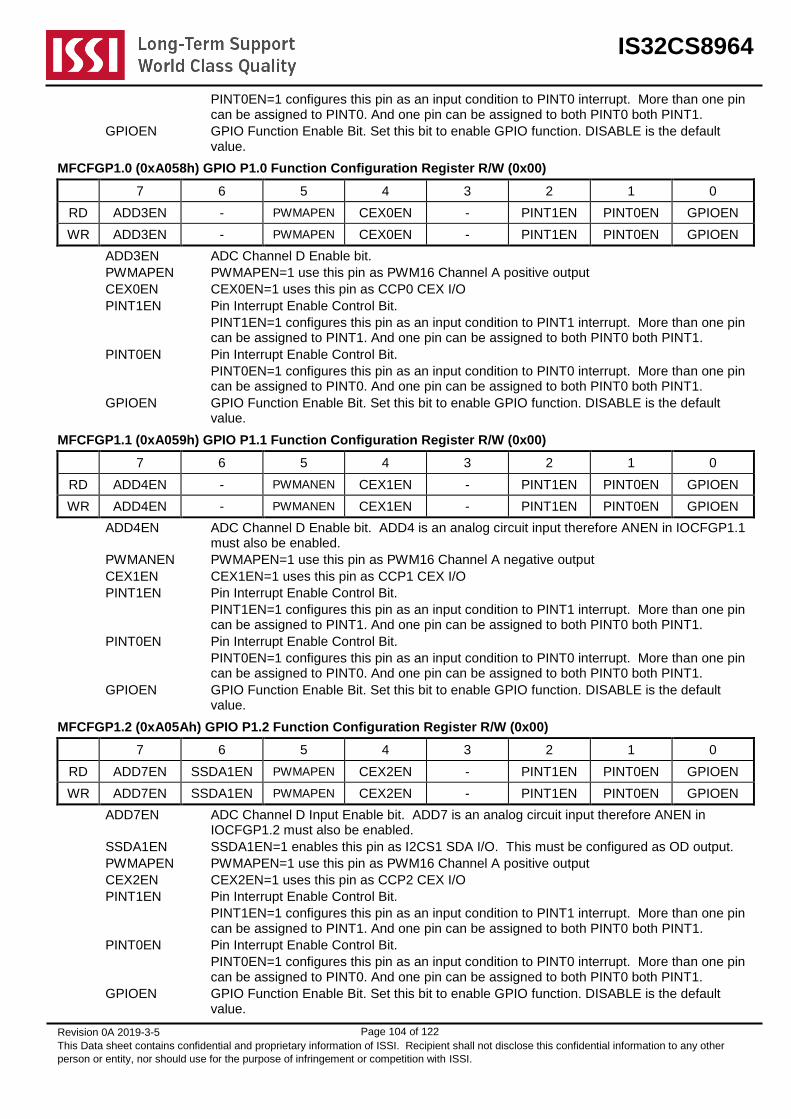
IS32CS8964
Revision 0A 2019-3-5
This Data sheet contains confidential and proprietary information of ISSI. Recipient shall not disclose this confidential information to any other
person or entity, nor should use for the purpose of infringement or competition with ISSI.
Page 104 of 122
PINT0EN=1 configures this pin as an input condition to PINT0 interrupt. More than one pin can be assigned to PINT0. And one pin can be assigned to both PINT0 both PINT1.
GPIOEN GPIO Function Enable Bit. Set this bit to enable GPIO function. DISABLE is the default value.
MFCFGP1.0 (0xA058h) GPIO P1.0 Function Configuration Register R/W (0x00)
7 6 5 4 3 2 1 0
RD ADD3EN - PWMAPEN CEX0EN - PINT1EN PINT0EN GPIOEN
WR ADD3EN - PWMAPEN CEX0EN - PINT1EN PINT0EN GPIOEN
ADD3EN ADC Channel D Enable bit.
PWMAPEN PWMAPEN=1 use this pin as PWM16 Channel A positive output
CEX0EN CEX0EN=1 uses this pin as CCP0 CEX I/O
PINT1EN Pin Interrupt Enable Control Bit.
PINT1EN=1 configures this pin as an input condition to PINT1 interrupt. More than one pin can be assigned to PINT1. And one pin can be assigned to both PINT0 both PINT1.
PINT0EN Pin Interrupt Enable Control Bit.
PINT0EN=1 configures this pin as an input condition to PINT0 interrupt. More than one pin can be assigned to PINT0. And one pin can be assigned to both PINT0 both PINT1.
GPIOEN GPIO Function Enable Bit. Set this bit to enable GPIO function. DISABLE is the default value.
MFCFGP1.1 (0xA059h) GPIO P1.1 Function Configuration Register R/W (0x00)
7 6 5 4 3 2 1 0
RD ADD4EN - PWMANEN CEX1EN - PINT1EN PINT0EN GPIOEN
WR ADD4EN - PWMANEN CEX1EN - PINT1EN PINT0EN GPIOEN
ADD4EN ADC Channel D Enable bit. ADD4 is an analog circuit input therefore ANEN in IOCFGP1.1 must also be enabled.
PWMANEN PWMAPEN=1 use this pin as PWM16 Channel A negative output
CEX1EN CEX1EN=1 uses this pin as CCP1 CEX I/O
PINT1EN Pin Interrupt Enable Control Bit.
PINT1EN=1 configures this pin as an input condition to PINT1 interrupt. More than one pin can be assigned to PINT1. And one pin can be assigned to both PINT0 both PINT1.
PINT0EN Pin Interrupt Enable Control Bit.
PINT0EN=1 configures this pin as an input condition to PINT0 interrupt. More than one pin can be assigned to PINT0. And one pin can be assigned to both PINT0 both PINT1.
GPIOEN GPIO Function Enable Bit. Set this bit to enable GPIO function. DISABLE is the default value.
MFCFGP1.2 (0xA05Ah) GPIO P1.2 Function Configuration Register R/W (0x00)
7 6 5 4 3 2 1 0
RD ADD7EN SSDA1EN PWMAPEN CEX2EN - PINT1EN PINT0EN GPIOEN
WR ADD7EN SSDA1EN PWMAPEN CEX2EN - PINT1EN PINT0EN GPIOEN
ADD7EN ADC Channel D Input Enable bit. ADD7 is an analog circuit input therefore ANEN in IOCFGP1.2 must also be enabled.
SSDA1EN SSDA1EN=1 enables this pin as I2CS1 SDA I/O. This must be configured as OD output.
PWMAPEN PWMAPEN=1 use this pin as PWM16 Channel A positive output
CEX2EN CEX2EN=1 uses this pin as CCP2 CEX I/O
PINT1EN Pin Interrupt Enable Control Bit.
PINT1EN=1 configures this pin as an input condition to PINT1 interrupt. More than one pin can be assigned to PINT1. And one pin can be assigned to both PINT0 both PINT1.
PINT0EN Pin Interrupt Enable Control Bit.
PINT0EN=1 configures this pin as an input condition to PINT0 interrupt. More than one pin can be assigned to PINT0. And one pin can be assigned to both PINT0 both PINT1.
GPIOEN GPIO Function Enable Bit. Set this bit to enable GPIO function. DISABLE is the default value.

IS32CS8964
Revision 0A 2019-3-5
This Data sheet contains confidential and proprietary information of ISSI. Recipient shall not disclose this confidential information to any other
person or entity, nor should use for the purpose of infringement or competition with ISSI.
Page 105 of 122
MFCFGP1.3 (0xA05Bh) GPIO P1.3 Function Configuration Register R/W (0x00)
7 6 5 4 3 2 1 0
RD ADD8EN SSCL1EN PWMANEN CEX3EN - PINT1EN PINT0EN GPIOEN
WR ADD8EN SSCL1EN PWMANEN CEX3EN - PINT1EN PINT0EN GPIOEN
ADD8EN ADC Channel D Input Enable bit. ADD8 is an analog circuit input therefore ANEN in IOCFGP1.3 must also be enabled.
SSCL1EN SSCL1EN=1 enables this pin as I2CS1 SCL I/O. This must be configured as OD output.
PWMANEN PWMANEN=1 use this pin as PWM16 Channel A negative output
CEX3EN CEX3EN=1 uses this pin as CCP3 CEX I/O
PINT1EN Pin Interrupt Enable Control Bit.
PINT1EN=1 configures this pin as an input condition to PINT1 interrupt. More than one pin can be assigned to PINT1. And one pin can be assigned to both PINT0 both PINT1.
PINT0EN Pin Interrupt Enable Control Bit.
PINT0EN=1 configures this pin as an input condition to PINT0 interrupt. More than one pin can be assigned to PINT0. And one pin can be assigned to both PINT0 both PINT1.
GPIOEN GPIO Function Enable Bit. Set this bit to enable GPIO function. DISABLE is the default value.
MFCFGP1.4 (0xA05Ch) GPIO P1.4 Function Configuration Register R/W (0x00)
7 6 5 4 3 2 1 0
RD RXOUTEN SSCL2EN PWMBPEN MSCLEN - PINT1EN PINT0EN GPIOEN
WR RXOUTEN SSCL2EN PWMBPEN MSCLEN - PINT1EN PINT0EN GPIOEN
RXOUTEN RTC Crystal Output Enable pin. RXOUT is an analog circuit output therefore ANEN in IOCFGP1.4 must also be enabled.
SSCL2EN SSCL2EN=1 enables this pin as I2CS2 SCL I/O. This must be configured as OD output.
PWMBPEN PWMBPEN=1 use this pin as PWM16 Channel B positive output.
MSCLEN MSCLEN=1 enables this pin as I2CM SCL I/O. This must be configured as OD output.
PINT1EN Pin Interrupt Enable Control Bit.
PINT1EN=1 configures this pin as an input condition to PINT1 interrupt. More than one pin can be assigned to PINT1. And one pin can be assigned to both PINT0 both PINT1.
PINT0EN Pin Interrupt Enable Control Bit.
PINT0EN=1 configures this pin as an input condition to PINT0 interrupt. More than one pin can be assigned to PINT0. And one pin can be assigned to both PINT0 both PINT1.
GPIOEN GPIO Function Enable Bit. Set this bit to enable GPIO function. DISABLE is the default value.
MFCFGP1.5 (0xA05Dh) GPIO P1.5 Function Configuration Register R/W (0x00)
7 6 5 4 3 2 1 0
RD RXINEN SSDA2EN PWMBNEN MSDAEN - PINT1EN PINT0EN GPIOEN
WR RXINEN SSDA2EN PWMBNEN MSDAEN - PINT1EN PINT0EN GPIOEN
RXINEN RTC Crystal IN Enable pin. RXIN is an analog circuit output therefore ANEN in IOCFGP1.5 must also be enabled.
SSDA2EN SSDA2EN=1 enables this pin as I2CS2 SDA I/O. This must be configured as OD output.
PWMBNEN PWMBNEN=1 use this pin as PWM16 Channel B negative output.
MSDAEN MSDAEN=1 enables this pin as I2CM SDA I/O. This must be configured as OD output.
PINT1EN Pin Interrupt Enable Control Bit.
PINT1EN=1 configures this pin as an input condition to PINT1 interrupt. More than one pin can be assigned to PINT1. And one pin can be assigned to both PINT0 both PINT1.
PINT0EN Pin Interrupt Enable Control Bit.
PINT0EN=1 configures this pin as an input condition to PINT0 interrupt. More than one pin can be assigned to PINT0. And one pin can be assigned to both PINT0 both PINT1.
GPIOEN GPIO Function Enable Bit. Set this bit to enable GPIO function. DISABLE is the default value.

IS32CS8964
Revision 0A 2019-3-5
This Data sheet contains confidential and proprietary information of ISSI. Recipient shall not disclose this confidential information to any other
person or entity, nor should use for the purpose of infringement or competition with ISSI.
Page 106 of 122
MFCFGP1.6 (0xA05Eh) GPIO P1.6 Function Configuration Register R/W (0x00)
7 6 5 4 3 2 1 0
RD ADD9EN T1EN PWMBPEN CEX0EN - PINT1EN PINT0EN GPIOEN
WR ADD9EN T1EN PWMBPEN CEX0EN - PINT1EN PINT0EN GPIOEN
ADD9EN ADC Channel D Input Enable bit. ADD9 is an analog circuit input therefore ANEN in IOCFGP1.6 must also be enabled.
T1EN T1EN=1 enables this pin as Timer 1 input. This must be configured as OD output.
PWMBPEN PWMBPEN=1 use this pin as PWM16 Channel B positive output.
CEX0EN CEX0EN=1 uses this pin as CCP0 CEX I/O.
PINT1EN Pin Interrupt Enable Control Bit.
PINT1EN=1 configures this pin as an input condition to PINT1 interrupt. More than one pin can be assigned to PINT1. And one pin can be assigned to both PINT0 both PINT1.
PINT0EN Pin Interrupt Enable Control Bit.
PINT0EN=1 configures this pin as an input condition to PINT0 interrupt. More than one pin can be assigned to PINT0. And one pin can be assigned to both PINT0 both PINT1.
GPIOEN GPIO Function Enable Bit. Set this bit to enable GPIO function. DISABLE is the default value.
MFCFGP1.7 (0xA05Fh) GPIO P1.7 Function Configuration Register R/W (0x00)
7 6 5 4 3 2 1 0
RD VDACEN T0EN PWMBNEN CEX1EN - PINT1EN PINT0EN GPIOEN
WR VDACEN T0EN PWMBNEN CEX1EN - PINT1EN PINT0EN GPIOEN
VDACEN Voltage DAC Output Enable bit. VDAC is an analog circuit output therefore ANEN in IOCFGP1.7 must also be enabled.
T0EN T0EN=1 enables this pin as Timer 0 input. This must be configured as OD output.
PWMBNEN PWMBNEN=1 use this pin as PWM16 Channel B negative output.
CEX1EN CEX1EN=1 uses this pin as CCP1 CEX I/O.
PINT1EN Pin Interrupt Enable Control Bit.
PINT1EN=1 configures this pin as an input condition to PINT1 interrupt. More than one pin can be assigned to PINT1. And one pin can be assigned to both PINT0 both PINT1.
PINT0EN Pin Interrupt Enable Control Bit.
PINT0EN=1 configures this pin as an input condition to PINT0 interrupt. More than one pin can be assigned to PINT0. And one pin can be assigned to both PINT0 both PINT1.
GPIOEN GPIO Function Enable Bit. Set this bit to enable GPIO function. DISABLE is the default value.
MFCFGP2.0 (0xA070h) GPIO P2.0 Function Configuration Register R/W (0x00)
7 6 5 4 3 2 1 0
RD XINEN MSCLEN SSCL1EN CEX4EN MOSIEN PINT1EN PINT0EN GPIOEN
WR XINEN MSCLEN SSCL1EN CEX4EN MOSIEN PINT1EN PINT0EN GPIOEN
XINEN Crystal IN Enable pin. XIN is an analog circuit output therefore ANEN in IOCFGP2.0 must also be enabled.
MSCLEN MSCLEN=1 enables this pin as I2CM SCL I/O. This must be configured as OD output.
SSCL1EN SSCL1EN=1 enables this pin as I2CSS1 SCL I/O. This must be configured as OD output.
CEX4EN CEX4EN=1 uses this pin as CCP4 CEX I/O.
MOSIEN MOSIEN=1 uses this pin as SPI MOSI I/O.
PINT1EN Pin Interrupt Enable Control Bit.
PINT1EN=1 configures this pin as an input condition to PINT1 interrupt. More than one pin can be assigned to PINT1. And one pin can be assigned to both PINT0 both PINT1.
PINT0EN Pin Interrupt Enable Control Bit.
PINT0EN=1 configures this pin as an input condition to PINT0 interrupt. More than one pin can be assigned to PINT0. And one pin can be assigned to both PINT0 both PINT1.
GPIOEN GPIO Function Enable Bit. Set this bit to enable GPIO function. DISABLE is the default value.

IS32CS8964
Revision 0A 2019-3-5
This Data sheet contains confidential and proprietary information of ISSI. Recipient shall not disclose this confidential information to any other
person or entity, nor should use for the purpose of infringement or competition with ISSI.
Page 107 of 122
MFCFGP2.1 (0xA071h) GPIO P2.1 Function Configuration Register R/W (0x00)
7 6 5 4 3 2 1 0
RD XOUTEN MSDAEN SSDA1EN CEX5EN MISOEN PINT1EN PINT0EN GPIOEN
WR XOUTEN MSDAEN SSDA1EN CEX5EN MISOEN PINT1EN PINT0EN GPIOEN
XOUTEN Crystal OUT Enable pin. XOUT is an analog circuit output therefore ANEN in IOCFGP2.1 must also be enabled.
MSDAEN MSDAEN=1 enables this pin as I2CM SDA I/O. This must be configured as OD output.
SSDA1EN SSDA1EN=1 enables this pin as I2CSS1 SDA I/O. This must be configured as OD output.
CEX5EN CEX5EN=1 uses this pin as CCP5 CEX I/O.
MISOEN MISOEN=1 uses this pin as SPI MISO I/O.
PINT1EN Pin Interrupt Enable Control Bit.
PINT1EN=1 configures this pin as an input condition to PINT1 interrupt. More than one pin can be assigned to PINT1. And one pin can be assigned to both PINT0 both PINT1.
PINT0EN Pin Interrupt Enable Control Bit.
PINT0EN=1 configures this pin as an input condition to PINT0 interrupt. More than one pin can be assigned to PINT0. And one pin can be assigned to both PINT0 both PINT1.
GPIOEN GPIO Function Enable Bit. Set this bit to enable GPIO function. DISABLE is the default value.
MFCFGP2.2 (0xA072h) GPIO P2.2 Function Configuration Register R/W (0x00)
7 6 5 4 3 2 1 0
RD VDACEN - XEMGEN TXD2EN SCKEN PINT1EN PINT0EN GPIOEN
WR VDACEN - XENGEN TXD2EN SCKEN PINT1EN PINT0EN GPIOEN
VDACEN Voltage DAC Output Enable bit. VDAC is an analog circuit output therefore ANEN in IOCFGP2.2 must also be enabled.
XEMGEN XEMGEN=1 enables this pin as EMG input of PWM16.
TXD2EN TXD2EN=1 uses this pin as EUART2 TXD output.
SCKEN SCKEN=1 uses this pin as SPI SCK I/O.
PINT1EN Pin Interrupt Enable Control Bit.
PINT1EN=1 configures this pin as an input condition to PINT1 interrupt. More than one pin can be assigned to PINT1. And one pin can be assigned to both PINT0 both PINT1.
PINT0EN Pin Interrupt Enable Control Bit.
PINT0EN=1 configures this pin as an input condition to PINT0 interrupt. More than one pin can be assigned to PINT0. And one pin can be assigned to both PINT0 both PINT1.
GPIOEN GPIO Function Enable Bit. Set this bit to enable GPIO function. DISABLE is the default value.
MFCFGP2.3 (0xA073h) GPIO P2.3 Function Configuration Register R/W (0x00)
7 6 5 4 3 2 1 0
RD CMPTHEN - XEMGEN RXD2EN SSNEN PINT1EN PINT0EN GPIOEN
WR CMPTHEN - XENGEN RXD2EN SSNEN PINT1EN PINT0EN GPIOEN
CMPTHEN Comparator External Threshold Enable bit. CMPTH is an analog circuit input therefore ANEN in IOCFGP2.3 must also be enabled.
XEMGEN XEMGEN=1 enables this pin as EMG input of PWM16.
RXD2EN RXD2EN=1 uses this pin as EUART2 RXD input.
SSNEN SSNEN=1 uses this pin as SPI SSN input.
PINT1EN Pin Interrupt Enable Control Bit.
PINT1EN=1 configures this pin as an input condition to PINT1 interrupt. More than one pin can be assigned to PINT1. And one pin can be assigned to both PINT0 both PINT1.
PINT0EN Pin Interrupt Enable Control Bit.
PINT0EN=1 configures this pin as an input condition to PINT0 interrupt. More than one pin can be assigned to PINT0. And one pin can be assigned to both PINT0 both PINT1.
GPIOEN GPIO Function Enable Bit. Set this bit to enable GPIO function. DISABLE is the default value.

IS32CS8964
Revision 0A 2019-3-5
This Data sheet contains confidential and proprietary information of ISSI. Recipient shall not disclose this confidential information to any other
person or entity, nor should use for the purpose of infringement or competition with ISSI.
Page 108 of 122
MFCFGP2.4 (0xA074h) GPIO P2.4 Function Configuration Register R/W (0x00)
7 6 5 4 3 2 1 0
RD CMPDEN - PWMCPEN T2EN - PINT1EN PINT0EN GPIOEN
WR CMPDEN - PWMCPEN T2EN - PINT1EN PINT0EN GPIOEN
CMPDEN Comparator D Input Enable bit. CMPD is an analog circuit input therefore ANEN in IOCFGP2.4 must also be enabled.
PWMCPEN PWMCPEN=1 use this pin as PWM16 Channel C positive output.
T2EN T2EN=1 uses this pin as Timer 2 Input.
PINT1EN Pin Interrupt Enable Control Bit.
PINT1EN=1 configures this pin as an input condition to PINT1 interrupt. More than one pin can be assigned to PINT1. And one pin can be assigned to both PINT0 both PINT1.
PINT0EN Pin Interrupt Enable Control Bit.
PINT0EN=1 configures this pin as an input condition to PINT0 interrupt. More than one pin can be assigned to PINT0. And one pin can be assigned to both PINT0 both PINT1.
GPIOEN GPIO Function Enable Bit. Set this bit to enable GPIO function. DISABLE is the default value.
MFCFGP2.5 (0xA075h) GPIO P2.5 Function Configuration Register R/W (0x00)
7 6 5 4 3 2 1 0
RD CMPCEN - PWMCNEN CEX4EN - PINT1EN PINT0EN GPIOEN
WR CMPCEN - PWMCNEN CEX4EN - PINT1EN PINT0EN GPIOEN
CMPCEN Comparator C Input Enable bit. CMPC is an analog circuit input therefore ANEN in IOCFGP2.5 must also be enabled.
PWMCNEN PWMCNEN=1 use this pin as PWM16 Channel C negative output.
CEX4EN CEX4EN=1 uses this pin as CCP4 CEX I/O.
PINT1EN Pin Interrupt Enable Control Bit.
PINT1EN=1 configures this pin as an input condition to PINT1 interrupt. More than one pin can be assigned to PINT1. And one pin can be assigned to both PINT0 both PINT1.
PINT0EN Pin Interrupt Enable Control Bit.
PINT0EN=1 configures this pin as an input condition to PINT0 interrupt. More than one pin can be assigned to PINT0. And one pin can be assigned to both PINT0 both PINT1.
GPIOEN GPIO Function Enable Bit. Set this bit to enable GPIO function. DISABLE is the default value.
MFCFGP2.6 (0xA076h) GPIO P2.6 Function Configuration Register R/W (0x00)
7 6 5 4 3 2 1 0
RD CMPBEN - XEMGEN CEX5EN SSNEN PINT1EN PINT0EN GPIOEN
WR CMPBEN - XEMGEN CEX5EN SSNEN PINT1EN PINT0EN GPIOEN
CMPBEN Comparator B Input Enable bit. CMPB is an analog circuit input therefore ANEN in IOCFGP2.6 must also be enabled.
XEMGEN XEMGEN=1 enables this pin as EMG input of PWM16.
CEX5EN CEX5EN=1 uses this pin as CCP5 CEX I/O.
SSNEN SSNEN=1 uses this pin as SPI SSN input.
PINT1EN Pin Interrupt Enable Control Bit.
PINT1EN=1 configures this pin as an input condition to PINT1 interrupt. More than one pin can be assigned to PINT1. And one pin can be assigned to both PINT0 both PINT1.
PINT0EN Pin Interrupt Enable Control Bit.
PINT0EN=1 configures this pin as an input condition to PINT0 interrupt. More than one pin can be assigned to PINT0. And one pin can be assigned to both PINT0 both PINT1.
GPIOEN GPIO Function Enable Bit. Set this bit to enable GPIO function. DISABLE is the default value.

IS32CS8964
Revision 0A 2019-3-5
This Data sheet contains confidential and proprietary information of ISSI. Recipient shall not disclose this confidential information to any other
person or entity, nor should use for the purpose of infringement or competition with ISSI.
Page 109 of 122
MFCFGP2.7 (0xA077h) GPIO P2.7 Function Configuration Register R/W (0x00)
7 6 5 4 3 2 1 0
RD CMPAEN - XEMGEN T2EXEN SCKEN PINT1EN PINT0EN GPIOEN
WR CMPAEN - XEMGEN T2EXEN SCKEN PINT1EN PINT0EN GPIOEN
CMPAEN Comparator A Input Enable bit. CMPA is an analog circuit input therefore ANEN in IOCFGP2.7 must also be enabled.
XEMGEN XEMGEN=1 enables this pin as EMG input of PWM16.
T2EXEN T2EXEN=1 enables this pin as T2EX input for Timer 2.
SCKEN SCKEN=1 uses this pin as SPI SCK I/O.
PINT1EN Pin Interrupt Enable Control Bit.
PINT1EN=1 configures this pin as an input condition to PINT1 interrupt. More than one pin can be assigned to PINT1. And one pin can be assigned to both PINT0 both PINT1.
PINT0EN Pin Interrupt Enable Control Bit.
PINT0EN=1 configures this pin as an input condition to PINT0 interrupt. More than one pin can be assigned to PINT0. And one pin can be assigned to both PINT0 both PINT1.
GPIOEN GPIO Function Enable Bit. Set this bit to enable GPIO function. DISABLE is the default value.
MFCFGP3.0 (0xA078h) GPIO P3.0 Function Configuration Register R/W (0x00)
7 6 5 4 3 2 1 0
RD ADD5EN - PWMCNEN CEX2EN - PINT1EN PINT0EN GPIOEN
WR ADD5EN - PWMCNEN CEX2EN - PINT1EN PINT0EN GPIOEN
ADD5EN ADC Channel D Input Enable bit. ADD5 is an analog circuit input therefore ANEN in IOCFGP3.0 must also be enabled.
PWMCNEN PWMCNEN=1 use this pin as PWM16 Channel C negative output.
CEX2EN CEX2EN=1 enable this pin as CCP2 CEX I/O.
PINT1EN Pin Interrupt Enable Control Bit.
PINT1EN=1 configures this pin as an input condition to PINT1 interrupt. More than one pin can be assigned to PINT1. And one pin can be assigned to both PINT0 both PINT1.
PINT0EN Pin Interrupt Enable Control Bit.
PINT0EN=1 configures this pin as an input condition to PINT0 interrupt. More than one pin can be assigned to PINT0. And one pin can be assigned to both PINT0 both PINT1.
GPIOEN GPIO Function Enable Bit. Set this bit to enable GPIO function. DISABLE is the default value.
MFCFGP3.1 (0xA079h) GPIO P3.1 Function Configuration Register R/W (0x00)
7 6 5 4 3 2 1 0
RD ADD6EN - PWMCPEN CEX3EN - PINT1EN PINT0EN GPIOEN
WR ADD6EN - PWMCPEN CEX3EN - PINT1EN PINT0EN GPIOEN
ADD6EN ADC Channel D Input Enable bit. ADD6 is an analog circuit input therefore ANEN in IOCFGP3.1 must also be enabled.
PWMCPEN PWMCPEN=1 use this pin as PWM16 Channel C positive output.
CEX3EN CEX3EN=1 enable this pin as CCP3 CEX I/O.
PINT1EN Pin Interrupt Enable Control Bit.
PINT1EN=1 configures this pin as an input condition to PINT1 interrupt. More than one pin can be assigned to PINT1. And one pin can be assigned to both PINT0 both PINT1.
PINT0EN Pin Interrupt Enable Control Bit.
PINT0EN=1 configures this pin as an input condition to PINT0 interrupt. More than one pin can be assigned to PINT0. And one pin can be assigned to both PINT0 both PINT1.
GPIOEN GPIO Function Enable Bit. Set this bit to enable GPIO function. DISABLE is the default value.

IS32CS8964
Revision 0A 2019-3-5
This Data sheet contains confidential and proprietary information of ISSI. Recipient shall not disclose this confidential information to any other
person or entity, nor should use for the purpose of infringement or competition with ISSI.
Page 110 of 122
MFCFGP3.2 (0xA07Ah) GPIO P3.2 Function Configuration Register R/W (0x00)
7 6 5 4 3 2 1 0
RD VDACEN - TXD2EN CEX4EN MOSIEN PINT1EN PINT0EN GPIOEN
WR VDACEN - TXD2EN CEX4EN MOSIEN PINT1EN PINT0EN GPIOEN
VDACEN Voltage DAC Output Enable bit. VDAC is an analog circuit output therefore ANEN in IOCFGP3.2 must also be enabled.
TXD2EN TXD2EN=1 uses this pin as EUART2 TXD output.
CEX4EN CEX4EN=1 enable this pin as CCP4 CEX I/O.
MOSIEN MOSIEN=1 uses this pin as SPI MOSI I/O.
PINT1EN Pin Interrupt Enable Control Bit.
PINT1EN=1 configures this pin as an input condition to PINT1 interrupt. More than one pin can be assigned to PINT1. And one pin can be assigned to both PINT0 both PINT1.
PINT0EN Pin Interrupt Enable Control Bit.
PINT0EN=1 configures this pin as an input condition to PINT0 interrupt. More than one pin can be assigned to PINT0. And one pin can be assigned to both PINT0 both PINT1.
GPIOEN GPIO Function Enable Bit. Set this bit to enable GPIO function. DISABLE is the default value.
MFCFGP3.3 (0xA07Bh) GPIO P3.3 Function Configuration Register R/W (0x00)
7 6 5 4 3 2 1 0
RD CMPAEN - RXD2EN CEX5EN MISOEN PINT1EN PINT0EN GPIOEN
WR CMPAEN - RXD2EN CEX5EN MISOEN PINT1EN PINT0EN GPIOEN
CMPAEN Comparator A Input Enable bit. CMPA is an analog circuit input therefore ANEN in IOCFGP2.7 must also be enabled.
RXD2EN RXD2EN=1 uses this pin as EUART2 RXD input.
CEX5EN CEX5EN=1 enable this pin as CCP5 CEX I/O.
MISOEN MISOEN=1 uses this pin as SPI MISO I/O.
PINT1EN Pin Interrupt Enable Control Bit.
PINT1EN=1 configures this pin as an input condition to PINT1 interrupt. More than one pin can be assigned to PINT1. And one pin can be assigned to both PINT0 both PINT1.
PINT0EN Pin Interrupt Enable Control Bit.
PINT0EN=1 configures this pin as an input condition to PINT0 interrupt. More than one pin can be assigned to PINT0. And one pin can be assigned to both PINT0 both PINT1.
GPIOEN GPIO Function Enable Bit. Set this bit to enable GPIO function. DISABLE is the default value.
The GPIO pins can be configured as external pin interrupt input or for wake up purpose. Each port has edge detection logic and latch for rising and falling edge detections.
PIOEDGR0 (0xA028h) Port0 IO Input Rising Edge Detection Register R/W (0x00)
7 6 5 4 3 2 1 0
RD PR0[7-0]
WR PREN0[7-0]
PR0[7-0] PORT0.0 to PORT0.7 Rising Edge Detection Status
PR0[i] is set by hardware when a rising edge is detected on PORT0.i input if PREN0[i]=0. PR0[i] is latched and must be cleared by software by writing PREN0[i]=0.
PR0[i] is also used to generate the PIN interrupt if corresponding port PINTEN is enabled.
PREN0[7-0] Port 0 Rising Edge Detection Enable
PREN0[i]=1 enables the rising edge detection.
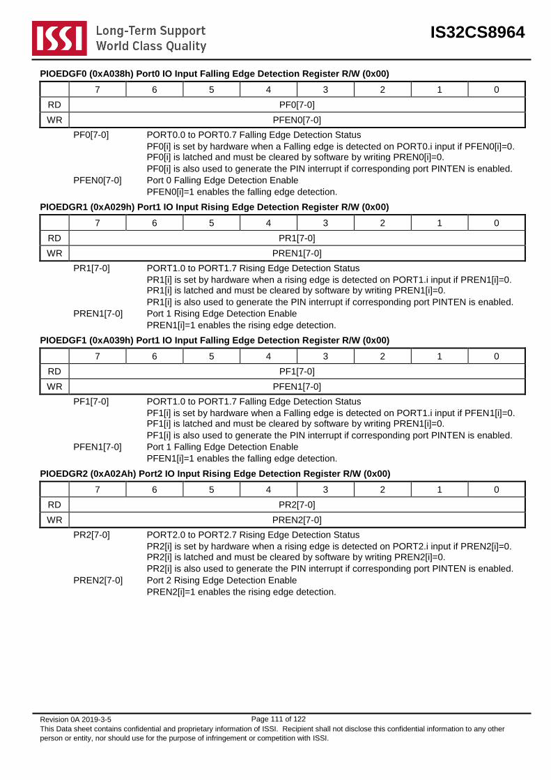
IS32CS8964
Revision 0A 2019-3-5
This Data sheet contains confidential and proprietary information of ISSI. Recipient shall not disclose this confidential information to any other
person or entity, nor should use for the purpose of infringement or competition with ISSI.
Page 111 of 122
PIOEDGF0 (0xA038h) Port0 IO Input Falling Edge Detection Register R/W (0x00)
7 6 5 4 3 2 1 0
RD PF0[7-0]
WR PFEN0[7-0]
PF0[7-0] PORT0.0 to PORT0.7 Falling Edge Detection Status
PF0[i] is set by hardware when a Falling edge is detected on PORT0.i input if PFEN0[i]=0. PF0[i] is latched and must be cleared by software by writing PREN0[i]=0.
PF0[i] is also used to generate the PIN interrupt if corresponding port PINTEN is enabled.
PFEN0[7-0] Port 0 Falling Edge Detection Enable
PFEN0[i]=1 enables the falling edge detection.
PIOEDGR1 (0xA029h) Port1 IO Input Rising Edge Detection Register R/W (0x00)
7 6 5 4 3 2 1 0
RD PR1[7-0]
WR PREN1[7-0]
PR1[7-0] PORT1.0 to PORT1.7 Rising Edge Detection Status
PR1[i] is set by hardware when a rising edge is detected on PORT1.i input if PREN1[i]=0. PR1[i] is latched and must be cleared by software by writing PREN1[i]=0.
PR1[i] is also used to generate the PIN interrupt if corresponding port PINTEN is enabled.
PREN1[7-0] Port 1 Rising Edge Detection Enable
PREN1[i]=1 enables the rising edge detection.
PIOEDGF1 (0xA039h) Port1 IO Input Falling Edge Detection Register R/W (0x00)
7 6 5 4 3 2 1 0
RD PF1[7-0]
WR PFEN1[7-0]
PF1[7-0] PORT1.0 to PORT1.7 Falling Edge Detection Status
PF1[i] is set by hardware when a Falling edge is detected on PORT1.i input if PFEN1[i]=0. PF1[i] is latched and must be cleared by software by writing PREN1[i]=0.
PF1[i] is also used to generate the PIN interrupt if corresponding port PINTEN is enabled.
PFEN1[7-0] Port 1 Falling Edge Detection Enable
PFEN1[i]=1 enables the falling edge detection.
PIOEDGR2 (0xA02Ah) Port2 IO Input Rising Edge Detection Register R/W (0x00)
7 6 5 4 3 2 1 0
RD PR2[7-0]
WR PREN2[7-0]
PR2[7-0] PORT2.0 to PORT2.7 Rising Edge Detection Status
PR2[i] is set by hardware when a rising edge is detected on PORT2.i input if PREN2[i]=0. PR2[i] is latched and must be cleared by software by writing PREN2[i]=0.
PR2[i] is also used to generate the PIN interrupt if corresponding port PINTEN is enabled.
PREN2[7-0] Port 2 Rising Edge Detection Enable
PREN2[i]=1 enables the rising edge detection.

IS32CS8964
Revision 0A 2019-3-5
This Data sheet contains confidential and proprietary information of ISSI. Recipient shall not disclose this confidential information to any other
person or entity, nor should use for the purpose of infringement or competition with ISSI.
Page 112 of 122
PIOEDGF2 (0xA03Ah) Port2 IO Input Falling Edge Detection Register R/W (0x00)
7 6 5 4 3 2 1 0
RD PF2[7-0]
WR PFEN2[7-0]
PF2[7-0] PORT2.0 to PORT2.7 Falling Edge Detection Status
PF2[i] is set by hardware when a Falling edge is detected on PORT2.i input if PFEN2[i]=0. PF2[i] is latched and must be cleared by software by writing PREN2[i]=0.
PF2[i] is also used to generate the PIN interrupt if corresponding port PINTEN is enabled.
PFEN2[7-0] Port 2 Falling Edge Detection Enable
PFEN2[i]=1 enables the falling edge detection.
PIOEDGR3 (0xA02Bh) Port3 IO Input Rising Edge Detection Register R/W (0x00)
7 6 5 4 3 2 1 0
RD PR3[7-0]
WR PREN3[7-0]
PR3[7-0] PORT3.0 to PORT3.7 Rising Edge Detection Status
PR3[i] is set by hardware when a rising edge is detected on PORT3.i input if PREN3[i]=0. PR3[i] is latched and must be cleared by software by writing PREN3[i]=0.
PR3[i] is also used to generate the PIN interrupt if corresponding port PINTEN is enabled.
PREN3[7-0] Port 3 Rising Edge Detection Enable
PREN3[i]=1 enables the rising edge detection.
PIOEDGF3 (0xA03Bh) Port3 IO Input Falling Edge Detection Register R/W (0x00)
7 6 5 4 3 2 1 0
RD PF3[7-0]
WR PFEN3[7-0]
PF3[7-0] PORT3.0 to PORT3.7 Falling Edge Detection Status
PF3[i] is set by hardware when a Falling edge is detected on PORT3.i input if PFEN3[i]=0. PF3[i] is latched and must be cleared by software by writing PREN3[i]=0.
PF3[i] is also used to generate the PIN interrupt if corresponding port PINTEN is enabled.
PFEN3[7-0] Port 3 Falling Edge Detection Enable
PFEN3[i]=1 enables the falling edge detection.
IS32CS8964
Revision 0A 2019-3-5
This Data sheet contains confidential and proprietary information of ISSI. Recipient shall not disclose this confidential information to any other
person or entity, nor should use for the purpose of infringement or competition with ISSI.
Page 113 of 122
14. IFB Block and Writer Mode and Boot Code/ISP
14.1 IFB Block
Except the main memory, the flash memory also contains a separate 256B Information Block (IFB). The IFB is partitioned into two parts. 00 to 3F range contains critical manufacture and calibration information. And 40 to FF range is user data which is one time programmable. The IFB cannot be erased but can be programmable through Flash Controller Command. IFB can be erased and written through Writer mode under privileged operations only, and should not be done by the user. The user data portion can only serves as One-Time-Programmable storage by the user. The following table shows the IFB contents.
ADDRESS TYPE DESCRIPTION
00 – 01 M IFB Version. 0x00 is MSB and 0x01 is LSB.
02 – 07 M Product Name. 0x02 and 0x03 is “CS”. These fields use ASCII coding.
08 – 09 M Package and Product Code
0A – 0B M Product Version and Revision. These fields use ASCII coding.
0C M
Flash Memory Size
This byte contains the effective FLASH memory variations. Each bit represents 1/16th of
the maximum memory size. For example the largest flash memory is 64KB, then BIT[7-0]=11111111 indicates 64KB. BIT[7-0]=00001111 indicates 32KB FLASH.
0D M
SRAM Memory Size
This byte contains the effective SRAM memory variations. Each bit represents 1/16th of
the maximum memory size. For example the largest flash memory is 2KB, then BIT[7-0]=11111111 indicates 2KB. BIT[7-0]=00001111 indicates 1KB SRAM.
0E – 0F M These bytes contain customer specific information and are used to differentiate shipment for specific customer. For standard distributions, these bytes remain for 0xFF.
10 M CP1 Information. This byte is written as 0x00 if CP1 is performed, otherwise 0xFF is present.
11 M CP2 Information. This byte is written as 0x00 if CP2 is performed, otherwise 0xFF is present.
12 M CP3 Version. This byte is written a value not equal to 0xFF to indicate CP3 is performed.
13 M CP3 BIN. The value is binary coding. If CP3 is not performed, this value is 0xFF.
14 M FT Version. This byte is written a value not equal to 0xFF to indicate FT is performed.
15 M FT BIN. The value is binary coding. If FT is not performed, this value is 0xFF.
16 – 1B M Last Test Date. These fields use ASCII coding.
1C – 1D M Boot Code Version. These two bytes contain the boot code version with two digits in ASCII code.
1E M Boot Code Segment. This byte contains the MSB byte of the address of the last instruction of the boot code. If no boot code is written, this value is 0xFF.
1F M Checksum for 0x00 – 0x1E. Checksum is the XOR results of all bytes.
20 M REGTRM value for 1.8V
21 M IOSC ITRM value for 16MHz
22 M IOSC VTRM value for 16MHz
23 M LVDTHD value for detection of 4.0V
24 M LVDTHD value for detection of 3.0V. If not calibrated, this byte should be written 0x00.
25 M IOSC ITRM value for 12MHz. If not calibrated, this byte should be written 0x00.
26 M IOSC VTRM value for 12MHz. If not calibrated, this byte should be written 0x00.
27 M IOSC ITRM value for 8MHz. If not calibrated, this byte should be written 0x00.
28 M IOSC VTRM value for 8MHz. If not calibrated, this byte should be written 0x00.
29 M IOSC ITRM value for 4MHz. If not calibrated, this byte should be written 0x00.
2A M IOSC VTRM value for 4MHz. If not calibrated, this byte should be written 0x00.
2B – 2C M Temperature Offset LSB/MSB. The ADC should use VDD18 as the full-scale reference. 0x2B is LSB and 0x2C is MSB. The upper 4-bit of the MSB is the offset of the calibration temperature from 20C. If not calibrated, these bytes should be written as 0x00.
2D M Temperature Coefficient. This byte contains the calibrated temperature coefficient for

IS32CS8964
Revision 0A 2019-3-5
This Data sheet contains confidential and proprietary information of ISSI. Recipient shall not disclose this confidential information to any other
person or entity, nor should use for the purpose of infringement or competition with ISSI.
Page 114 of 122
ADDRESS TYPE DESCRIPTION
10C in LSB of ADC. This is a binary number in 4.4 formats, i.e. the radix point is between bit 4 and bit 3. For example, 0b1011.1010 refers to 11.625 LSB. If calibration of temperature sensor is not done, then these two bytes should be written as 0x00.
2E – 2F M Internal Reference LSB/MSB
30 – 38 M Reserved. These bytes are reserved for future extensions and should be written as 0x00.
39 M Checksum for 0x20 – 0x39. Checksum is the XOR results of all bytes.
3A – 3F M Retention Value. These bytes are used to check general flash retention conditions.
40 M/U
Boot Code Wait Time. Boot code uses this byte to determine the ISP wait-time. This wait-time is necessary for stable ISP. After user program download, the wait time can be reduced to minimize power-on time.
Each “1” in bit [1-0] constitute 1 second and bits [3-2] constitute 2 second and bits [7-6] are I2CSCL2 and I2CSCL1 check. For example, 0b10000111 is 4 second waits time and also checks I2CSCL2 pad status. If I2CSCL2 is low, then wait time of 6 second is used regardless of bit [3-0] setting. The maximum wait time is 6 second, and minimum wait time is 0 second.
41 – FF U User One-Time Programmable Space
Note 1: M data cannot be modified and can only be written in writer mode when the entire Flash is erased.
Note 2: U data reads out as FF after the Flash is erased. It can only be programmed once after the Flash is mass erased.
****** The erasure of IFB or modifications of manufacture information in IFB void any manufacture warranty.
**** This table is for reference only. Please refer to most updated AP note and boot code documents.
14.2 Writer Mode
Writer Mode (WM) is used by the manufacturer or by users to program the flash (including IFB) through a dedicated hardware (Writer or Gang Writer). Under this set up, only WM related pins should be connected and all other unused pins left floating. Writer mode follows a proprietary protocol and is not released to general users. Users must obtain it through a formal written request to the manufacturer and must sign a strict Non-Disclosure-Agreement.
The Writer Mode provides the following commands.
ERASE Main Memory
ERASE Main Memory and IFB
READ AND VERIFY Main Memory (8-Byte)
WRITE BYTE Main Memory
READ BYTE IFB
WRITE BYTE IFB
Fast Continuous WRITE
Fast Continuous READ
The writer mode is protected against code piracy. The power-on state of the device deactivates the writer mode. Only ERASEMM and ERASEMMIFB, and READVERIFYMM commands can be executed. It is activated by READVERIFY the range of 0x0FFF8 to 0x0FFFF where a security key can be placed by the user program. The probability of guessing the key is 1 in 2^64 = 1.8E19. Since each trial of READVERIFY takes 10usec, it takes about 6E6 years to exhaust the combinations. If the key is unknown, a user can choose to issue the ERASEMM command then fully erase the entire contents (including the key). Once fully erased, all data in the flash is 0xFF, and it can be successfully unlocked by READVERIFYMM with 8-bytes of 0xFF.
The users must not erase the information in IFB. And the user should not modify the manufacturer data. Any violation of this results in the void of manufacturer warranty.
IS32CS8964
Revision 0A 2019-3-5
This Data sheet contains confidential and proprietary information of ISSI. Recipient shall not disclose this confidential information to any other
person or entity, nor should use for the purpose of infringement or competition with ISSI.
Page 115 of 122
14.2.1 Writer Mode Pins
PIN PIN# TYPE WRITER MODE PIN DESCRIPTION
VDD 20 P VDD should be connected to a solid 5.0V supply with good decoupling to VSS
VSS 32 G Tie to 0V and have good decoupling to VDD
VDD18 19 PO Have a 4.7uF and a 0.1uF good decoupling to VSS
RSTN 21 IN Pull to 5.0V through 1KOhm to enter to WRITER Mode.
P2.3 28 O BUSY status
P2.4 27 O TDO Data Output
P2.5 26 I TDI Data Input
P2.6 25 I TCLK Clock Input
P2.7 24 I TENB Test Enable Input. Low assertion.
14.3 Boot Code and In-System-Programming
After production testing of the packaged devices, the manufacture writes the manufacturer information and calibration data in the IFB. At the last stage, it writes a fixed boot-code in the main memory residing from 0x0F000 to 0xFFF8. The boot code is executed after resets. Firstly, the boot code scans the I
2C slave 1 and 2, as well as UART0
for any In-System-Programming request. This scanning takes about 10msec. If any valid request is valid during the scan, the host must send 'HOSTMD' command in the Boot Code wait time. Upon time out of the wait time, the boot code performs the cleanup and exit to user code. the boot-code proceeds to follow the request and performs the programming from the host. The default ISP commands available are
HOSTMD
UNLOCK
READ AND VERIFY Main Memory (8-Byte)
ERASE Main Memory exclude Boot Code
ERASE SECTOR Main Memory
WRITE BYTE Main Memory
SET ADDRESS
CONTINUOUSE WRITE
CONTINUOUS READ
READ BYTE IFB
WRITE BYTE IFB
Similar to writer mode, ISP is in default locked state. No command is accepted under locked state. To unlock the ISP, an 8-byte READVERIFY of 0x0FFF8 to 0x0FFFF must be successfully executed. Thus default ISP boot program provides similar code security as the Writer mode.
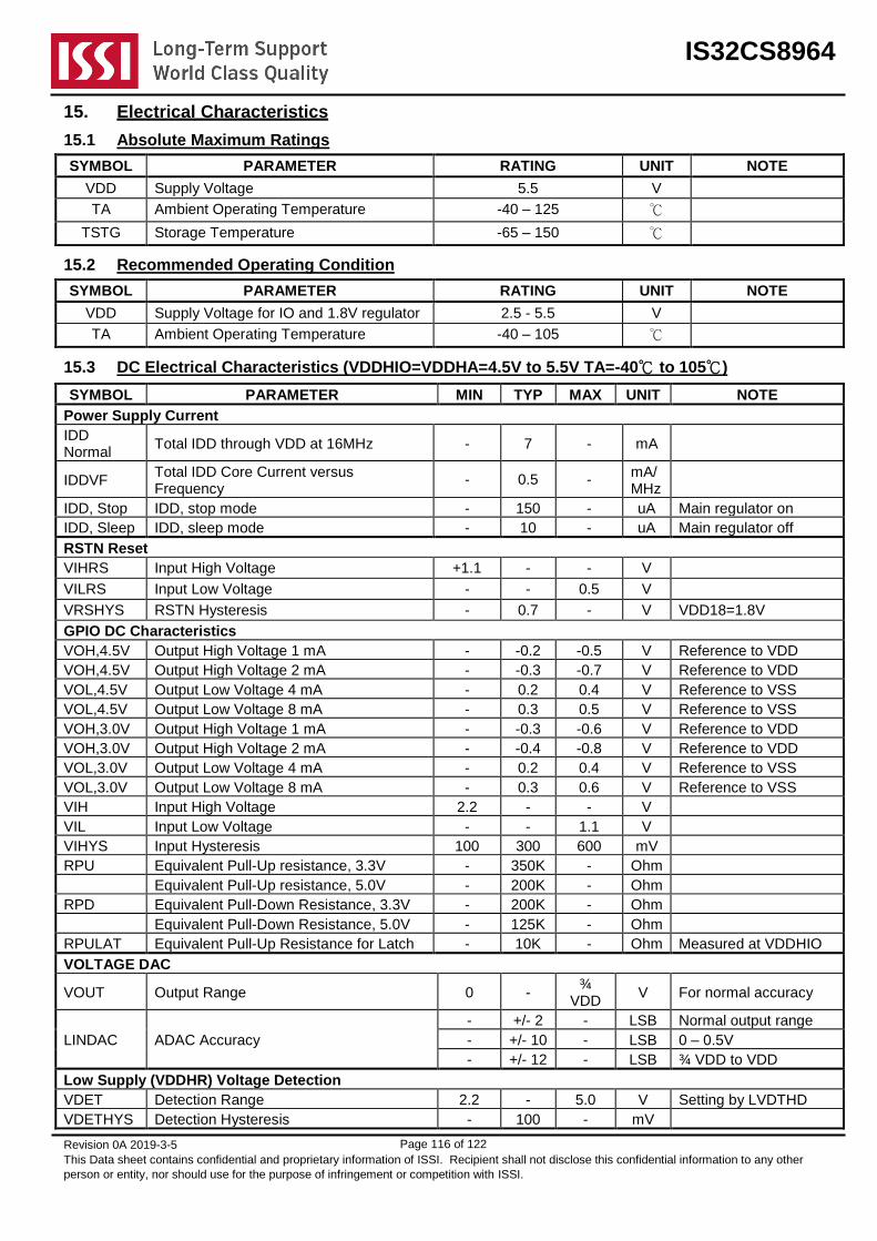
IS32CS8964
Revision 0A 2019-3-5
This Data sheet contains confidential and proprietary information of ISSI. Recipient shall not disclose this confidential information to any other
person or entity, nor should use for the purpose of infringement or competition with ISSI.
Page 116 of 122
15. Electrical Characteristics
15.1 Absolute Maximum Ratings
SYMBOL PARAMETER RATING UNIT NOTE
VDD Supply Voltage 5.5 V
TA Ambient Operating Temperature -40 – 125 ℃
TSTG Storage Temperature -65 – 150 ℃
15.2 Recommended Operating Condition
SYMBOL PARAMETER RATING UNIT NOTE
VDD Supply Voltage for IO and 1.8V regulator 2.5 - 5.5 V
TA Ambient Operating Temperature -40 – 105 ℃
15.3 DC Electrical Characteristics (VDDHIO=VDDHA=4.5V to 5.5V TA=-40℃ to 105℃)
SYMBOL PARAMETER MIN TYP MAX UNIT NOTE
Power Supply Current
IDD Normal
Total IDD through VDD at 16MHz - 7 - mA
IDDVF Total IDD Core Current versus Frequency
- 0.5 - mA/MHz
IDD, Stop IDD, stop mode - 150 - uA Main regulator on
IDD, Sleep IDD, sleep mode - 10 - uA Main regulator off
RSTN Reset
VIHRS Input High Voltage +1.1 - - V
VILRS Input Low Voltage - - 0.5 V
VRSHYS RSTN Hysteresis - 0.7 - V VDD18=1.8V
GPIO DC Characteristics
VOH,4.5V Output High Voltage 1 mA - -0.2 -0.5 V Reference to VDD
VOH,4.5V Output High Voltage 2 mA - -0.3 -0.7 V Reference to VDD
VOL,4.5V Output Low Voltage 4 mA - 0.2 0.4 V Reference to VSS
VOL,4.5V Output Low Voltage 8 mA - 0.3 0.5 V Reference to VSS
VOH,3.0V Output High Voltage 1 mA - -0.3 -0.6 V Reference to VDD
VOH,3.0V Output High Voltage 2 mA - -0.4 -0.8 V Reference to VDD
VOL,3.0V Output Low Voltage 4 mA - 0.2 0.4 V Reference to VSS
VOL,3.0V Output Low Voltage 8 mA - 0.3 0.6 V Reference to VSS
VIH Input High Voltage 2.2 - - V
VIL Input Low Voltage - - 1.1 V
VIHYS Input Hysteresis 100 300 600 mV
RPU Equivalent Pull-Up resistance, 3.3V - 350K - Ohm
Equivalent Pull-Up resistance, 5.0V - 200K - Ohm
RPD Equivalent Pull-Down Resistance, 3.3V - 200K - Ohm
Equivalent Pull-Down Resistance, 5.0V - 125K - Ohm
RPULAT Equivalent Pull-Up Resistance for Latch - 10K - Ohm Measured at VDDHIO
VOLTAGE DAC
VOUT Output Range 0 - ¾
VDD V For normal accuracy
LINDAC ADAC Accuracy
- +/- 2 - LSB Normal output range
- +/- 10 - LSB 0 – 0.5V
- +/- 12 - LSB ¾ VDD to VDD
Low Supply (VDDHR) Voltage Detection
VDET Detection Range 2.2 - 5.0 V Setting by LVDTHD
VDETHYS Detection Hysteresis - 100 - mV
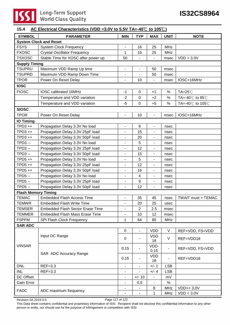
IS32CS8964
Revision 0A 2019-3-5
This Data sheet contains confidential and proprietary information of ISSI. Recipient shall not disclose this confidential information to any other
person or entity, nor should use for the purpose of infringement or competition with ISSI.
Page 117 of 122
15.4 AC Electrical Characteristics (VDD =3.0V to 5.5V TA=-40℃ to 105℃)
SYMBOL PARAMETER MIN TYP MAX UNIT NOTE
System Clock and Reset
FSYS System Clock Frequency - 16 25 MHz
FXOSC Crystal Oscillator Frequency 1 16 25 MHz
TSXOSC Stable Time for XOSC after power up 50 - - msec VDD > 3.0V
Supply Timing
TSUPRU Maximum VDD Ramp Up time - - 50 msec
TSUPRD Maximum VDD Ramp Down Time - - 50 msec
TPOR Power On Reset Delay - 10 - msec IOSC=16MHz
IOSC
FIOSC IOSC calibrated 16MHz -1 0 +1 % TA=25℃
Temperature and VDD variation -2 0 +2 % TA=-40℃ to 85℃
Temperature and VDD variation -5 0 +5 % TA=-40℃ to 105℃
SIOSC
TPOR Power On Reset Delay - 10 - msec IOSC=16MHz
IO Timing
TPD3 ++ Propagation Delay 3.3V No load - 6 - nsec
TPD3 ++ Propagation Delay 3.3V 25pF load - 15 - nsec
TPD3 ++ Propagation Delay 3.3V 50pF load - 20 - nsec
TPD3 -- Propagation Delay 3.3V No load - 5 - nsec
TPD3 -- Propagation Delay 3.3V 25pF load - 12 - nsec
TPD3 -- Propagation Delay 3.3V 50pF load - 15 - nsec
TPD5 ++ Propagation Delay 3.3V No load - 5 - nsec
TPD5 ++ Propagation Delay 3.3V 25pF load - 12 - nsec
TPD5 ++ Propagation Delay 3.3V 50pF load - 16 - nsec
TPD5 -- Propagation Delay 3.3V No load - 4 - nsec
TPD5 -- Propagation Delay 3.3V 25pF load - 9 - nsec
TPD5 -- Propagation Delay 3.3V 50pF load - 12 - nsec
Flash Memory Timing
TEMAC Embedded Flash Access Time - 35 45 nsec TWAIT must > TEMAC
TEMWR Embedded Flash Write Time - 20 25 usec
TEMSER Embedded Flash Sector Erase Time - 2 2.5 msec
TEMMER Embedded Flash Mass Erase Time - 10 12 msec
FSPFM SPI Flash Clock Frequency 1 64 80 MHz
SAR ADC
VINSAR
Input DC Range
0 - VDD V REF=VDD, FS=VDD
0 - VDD18
V REF=VDD18
SAR ADC Accuracy Range
0.15 - VDD-0.15
- REF=VDD, FS=VDD
0.15 - VDD18
- REF=VDD18
DNL REF=3.3 - - +/- 1 LSB
INL REF=3.3 - - +/- 4 LSB
DC Offset - +/- 10 - mV
Gain Error - 0.5 - %
FADC ADC maximum frequency - - 8 MHz VDD>= 3.0V
- - 1 MHz VDD < 3.0V
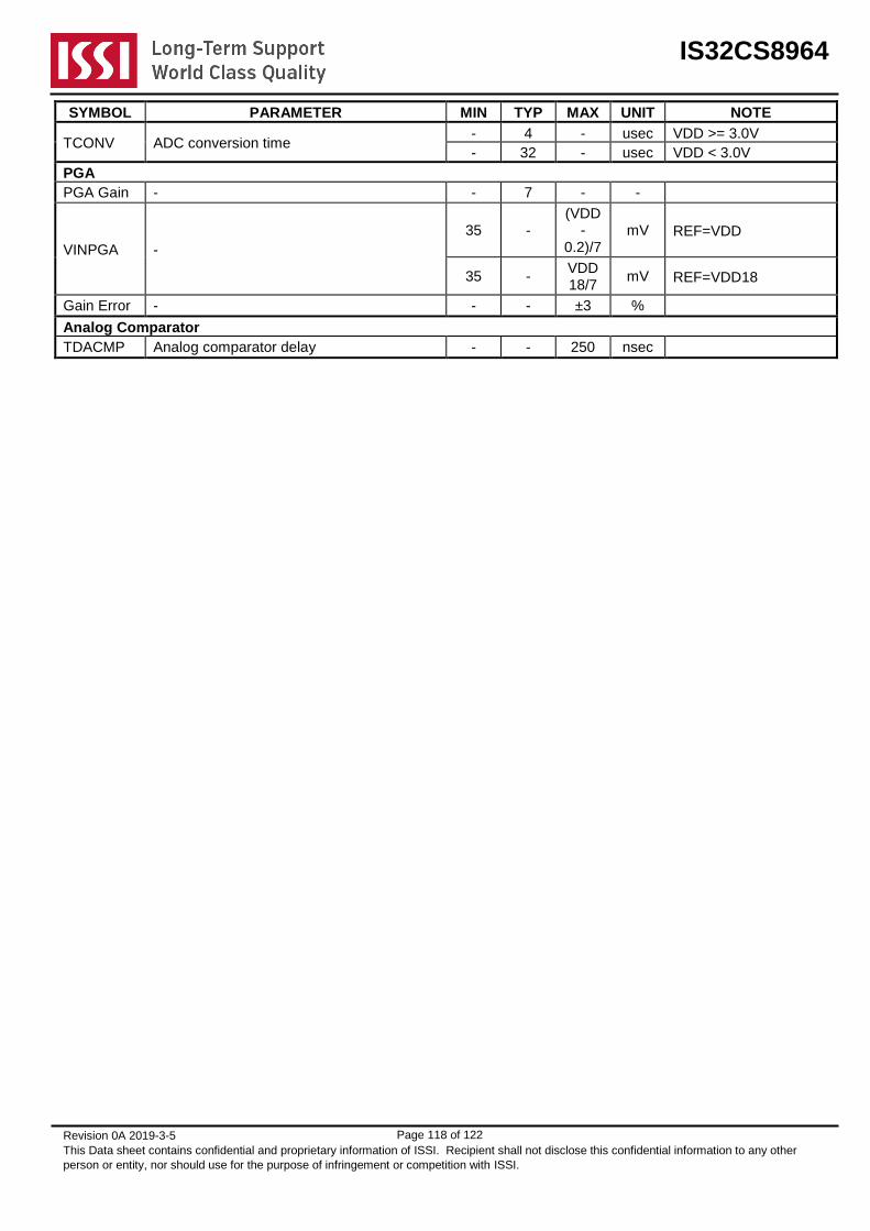
IS32CS8964
Revision 0A 2019-3-5
This Data sheet contains confidential and proprietary information of ISSI. Recipient shall not disclose this confidential information to any other
person or entity, nor should use for the purpose of infringement or competition with ISSI.
Page 118 of 122
SYMBOL PARAMETER MIN TYP MAX UNIT NOTE
TCONV ADC conversion time - 4 - usec VDD >= 3.0V
- 32 - usec VDD < 3.0V
PGA
PGA Gain - - 7 - -
VINPGA -
35 - (VDD
-0.2)/7
mV REF=VDD
35 - VDD18/7
mV REF=VDD18
Gain Error - - - ±3 %
Analog Comparator
TDACMP Analog comparator delay - - 250 nsec

IS32CS8964
Revision 0A 2019-3-5
This Data sheet contains confidential and proprietary information of ISSI. Recipient shall not disclose this confidential information to any other
person or entity, nor should use for the purpose of infringement or competition with ISSI.
Page 119 of 122
16. PACKAGE OUTLINE
32-pin QFN
L K
16 9
8
1
25
24
17
E2
D2
D
E
C0.35X45o
b
e
A1
A3
A
0.0
8 M
AX
.C
C
2
32
Symbol Dimensions in Millimeters
MIN. NOM. MAX.
A 0.70 0.75 0.80
A1 0.00 0.02 0.05
A3 0.203 REF.
b 0.18 0.25 0.30
D 4.90 5.00 5.10
E 4.90 5.00 5.10
e 0.50 BSC.
L 0.35 0.40 0.45
K 0.20 - -
NOTES:
1. JEDEC OUTLINE: N/A
2. DIMENSION b APPLIES TO METALLIZED TERMINAL AND IS MEASURED BETWEEN 0.15mm AND 0.30mm FROM THE TERMINAL TIP. IF THE TERMINAL HAS THE OPTIONAL RADIUS ON THE OTHER END OF THE TERMINAL. THE DIMENSION b SHOULD NOT BE MEASURED IN THAT RADIUS AREA.
3. THE MINIMUM “K” VALUE OF 0.20mm APPLIES.
4. BILATERAL COPLANARITY ZONE APPLIES TO THE EXPOSED HEAT SINK SLUG AS WELL AS THE TERMINALS.
Dimensions in Millimeters
D2 E2
EXPOSED PAD MIN. NOM. MAX. MIN. NOM. MAX.
3.2X3.2 3.10 3.20 3.30 3.10 3.20 3.30

IS32CS8964
Revision 0A 2019-3-5
This Data sheet contains confidential and proprietary information of ISSI. Recipient shall not disclose this confidential information to any other
person or entity, nor should use for the purpose of infringement or competition with ISSI.
Page 120 of 122
17. ORDERING INFORMATION
Operating temperature -40°C to 105°C
Order Part No. Package QTY
IS32CS8964-QWLA2 QFN-32, Lead-free 490/Tray
DISCLAIMER AND DECLARATION 1. Copyright © 2018 Integrated Silicon Solution, Inc. All rights reserved. ISSI reserves the right to make changes to
this specification and its products at any time without notice. ISSI assumes no liability arising out of the application or use of any information, products or services described herein. Customers are advised to obtain the latest version of this device specification before relying on any published information and before placing orders for products. Integrated Silicon Solution, Inc. does not recommend the use of any of its products in life support applications where the failure or malfunction of the product can reasonably be expected to cause failure of the life support system or to significantly affect its safety or effectiveness. Products are not authorized for use in such applications unless Integrated Silicon Solution, Inc. receives written assurance to its satisfaction, that: a.) The risk of injury or damage has been minimized; b.) The user assume all such risks; and c.) Potential liability of Integrated Silicon Solution, Inc is adequately protected under the circumstances.
2. Applications in medical appliances, life support devices system or flight vehicle using ISSI’s products are not authorized without express written approval of ISSI.

IS32CS8964
Revision 0A 2019-3-5
This Data sheet contains confidential and proprietary information of ISSI. Recipient shall not disclose this confidential information to any other
person or entity, nor should use for the purpose of infringement or competition with ISSI.
Page 121 of 122
18. Revision History
Revision 0A
1. Revise register map XFR table PWMCH (0xA085), PWMCNTH (0xA08B), TL5 (0xA004), TH5 (0xA005), TT5 (0xA006).
2. Revise register map SFR table TL4 (0xAC), TH4 (0xAD), TL3 (0xAE), TH3 (0xAF).
3. Revise bit-name EWDI at bit4 of EXIE (0xE8)
4. Revise bit-name DBGST and DBGWDTEN at bit0 and bit6 of BPCTRL (A0E3h)
5. Modify timer 2 block diagram in section 1.12
6. Revise I2C master speed description at I2CMTP (0xF7h)
7. Add description at SCON2 (0xC2)
8. Revise register name LINCTRL (0xA090), LINCNTRH (0xA091), LINCNTRL (0xA092), LINSBRH (0xA093), LINSBRL (0xA094) and LININT (0xA095) in section 5
9. Revise TUDR at SPIST (0xA3)
10. Modify 16-Bit Capture Mode diagram in section 7.1
11. Add description at PWM16EMG (0xA097h)
12. Revise RTCEN at XOSCCFG (A007h)
13. Revise RTCSCND0 (0xA008)
14. Revise SPIDAT (0xA4)
15. Revise CEX5EN at MFCFGP2.1 (0xA071h) and at MFCFGP2.6 (0xA076h)
16. The NACK in I2CSSTI and I2CSST2 cannot be cleared by S/W
V1.31
1. Update order part no.
V1.3
1. Update IOSC trim setting while ITRM[1-0]=00
2. Remove the STATUS (0xC5) description from section 1.2 and merge it into section 1.7
3. Revise TCON
V1.2
1. Update 16-bit PWM Controller
2. Add IPOL description in IO Buffer Configuration
V 1.1
1. Change product description
2. Update IFB table with the AP note v1.2
V 1.0
1. Revise PGA gain error to ±3%
V0.92
1. Revise RDA description and add some LIN controller description in EUART2
2. Revise TCON description
3. Remove UART2 and T3 from PMM and IDLE mode description
3. Add STEPCTRL
4. Revise I2CMCR
5. Add QFN-32 package and remove SSOP-28 package
6. Add WKDLY into CKSEL, and the recommend value is 0xF
7. Recommend a 4.7uF decoupling capacitor for VDDC pad in PIN DESCRIPTIONS
8. Modify IOSC adjusted range from 8MHz to 16MHz
9. Add 7X PGA into ADC CHDSEL[1-0] and the figure

IS32CS8964
Revision 0A 2019-3-5
This Data sheet contains confidential and proprietary information of ISSI. Recipient shall not disclose this confidential information to any other
person or entity, nor should use for the purpose of infringement or competition with ISSI.
Page 122 of 122
V0.90
1. Change LVD detection description
2. Change RSTN VIH=1.0V VIL=0.5V
3. P04 and P05 ADC channel change
4. Other misc. typing error