energy meter ic family - maxim integrated · 71m6531/71m6533/71m6534 . energy meter ic family ....
TRANSCRIPT

71M6531/71M6533/71M6534 Energy Meter IC Family
SOFTWARE USER’S GUIDE
5/8/2008
TERIDIAN Semiconductor Corporation 6440 Oak Canyon Rd., Suite 100
Irvine, CA 92618-5201
Ph: (714) 508-8800 ▪ Fax: (714) 508-8878
http://www.teridian.com/

71M653X Software User’s Guide
v1.1 TERIDIAN Proprietary 2 of 116
© Copyright 2005-2008 TERIDIAN Semiconductor Corporation
TERIDIAN Semiconductor Corporation makes no warranty for the use of its products, other than expressly contained in the Company’s warranty detailed in the TERIDIAN Semiconductor Corporation standard Terms and Conditions. The company assumes no responsibility for any errors which may appear in this document, reserves the right to change devices or specifications detailed herein at any time without notice and does not make any commitment to update the information contained herein.

71M653X Software User’s Guide
v1.1 TERIDIAN Proprietary 3 of 116
© Copyright 2005-2008 TERIDIAN Semiconductor Corporation
71M653X Energy Meter IC FAMILY
SOFTWARE USER’S GUIDE
71M653X Software User’s Guide
Table of Contents1 INTRODUCTION............................................................................................................................ 11
1.1 Using this Document .............................................................................................................. 11 1.2 Related Documentation ......................................................................................................... 12 1.3 Compatibility Statement ......................................................................................................... 12
2 DESIGN GUIDE ............................................................................................................................. 13 2.1 Hardware Requirements ........................................................................................................ 13 2.2 Software Requirements ......................................................................................................... 13 2.3 Software Architecture ............................................................................................................ 14 2.4 Utilities ..................................................................................................................................... 15 2.4.1 D_MERGE ............................................................................................................................. 15 2.4.2 CE_MERGE ........................................................................................................................... 15 2.4.3 BANK_MERGE ...................................................................................................................... 16
3 DESIGN REFERENCE .................................................................................................................. 17 3.1 Program Memory .................................................................................................................... 17 3.2 Data Memory ........................................................................................................................... 17 3.3 Programming the 71M653X Chips ........................................................................................ 18 3.4 Debugging of the 71M653X Chips ......................................................................................... 18 3.5 Test Tools ................................................................................................................................ 18 3.5.1 Running the 653X_Demo.hex Program.................................................................................. 19 3.5.2 CLI Commands ...................................................................................................................... 20 3.5.3 Command (Macro) Files ......................................................................................................... 20
4 TOOL INSTALLATION GUIDE ..................................................................................................... 21 4.1 Installing the Programs for the ADM51 Emulator ............................................................... 21 4.2 Installing the Wemu Program (Chameleon Debugger) ....................................................... 21 4.3 Installing the ADM51 USB Driver .......................................................................................... 22 4.4 Installing Updates to the Emulator Program and Hardware .............................................. 23 4.5 Creating a Project ................................................................................................................... 24 4.6 Installing the Keil Compiler ................................................................................................... 27 4.7 Creating a Project for the Keil Compiler .............................................................................. 28 4.7.1 Directory Structure ................................................................................................................. 28 4.7.2 Adjusting the Keil Compiler Settings ...................................................................................... 29 4.7.3 Manually Controlling the Keil Compiler Settings ..................................................................... 30 4.8 Output File Format .................................................................................................................. 32 4.8.1 Basic Intel Hex Format ........................................................................................................... 33 4.8.2 Intel Hex386 File Format ........................................................................................................ 34 4.9 Writing Bank-Switched Code ................................................................................................ 35 4.9.1 Hardware Overview ................................................................................................................ 35 4.9.2 Software Overview ................................................................................................................. 35 4.9.3 Software Tool Versions .......................................................................................................... 36
v1.1v1.1 TERIDIAN Proprietary 4 of 116
© Copyright 2005-2008 TERIDIAN Semiconductor Corporation
71M653X Software User’s Guide
4.9.4 Setup of the Compiler Project ................................................................................................ 36 4.9.5 Startup ................................................................................................................................... 37 4.9.6 Bank-Switching Code ............................................................................................................. 37 4.9.7 Page Table Setup and Debug ................................................................................................ 37 4.9.8 Producing a Banked Hex File ................................................................................................. 39 4.9.9 Placing Interrupts in Banked Code ......................................................................................... 39 4.9.10 Calling Banked Functions via Function Pointers .................................................................... 39 4.9.11 Putting Constants in Banks .................................................................................................... 40 4.9.12 Write-Protecting Flash in the 653X ......................................................................................... 40 4.10 Project Management Tools .................................................................................................... 41 4.11 Alternative Compilers ............................................................................................................. 41 4.12 Alternative Editors .................................................................................................................. 41 4.13 Alternative Linkers ................................................................................................................. 42
5 Demo Code Description .............................................................................................................. 43 5.1 80515 Data Types and Compiler-Specific Information ....................................................... 43 5.1.1 Data Types ............................................................................................................................. 43 5.1.2 Compiler-Specific Information ................................................................................................ 46 5.2 Demo Code Options and Program Size................................................................................ 47 5.3 Program Flow .......................................................................................................................... 51 5.3.1 Startup and Initialization ......................................................................................................... 52 5.4 Basic Code Architecture ........................................................................................................ 52 5.4.1 Initialization ............................................................................................................................ 53 5.4.2 Interrupts ................................................................................................................................ 53
5.4.2.1 Pulse Counting Interrupts ................................................................................................ 54 5.4.2.2 FWCOL0 and FWCOL1 ................................................................................................... 55 5.4.2.3 CE_BUSY Interrupt .......................................................................................................... 55 5.4.2.4 PLL_ISR ........................................................................................................................... 55 5.4.2.5 EEPROM Isr ..................................................................................................................... 56 5.4.2.6 Timer Interrupt .................................................................................................................. 56 5.4.2.7 The XFER_BUSY, RTC and NEAR_OVERFLOW Interrupt ............................................ 56 5.4.2.8 SERIAL Interrupt .............................................................................................................. 57
5.4.3 Background Tasks ................................................................................................................. 57 5.4.3.1 meter_run() ...................................................................................................................... 57 5.4.3.2 Command Line Interpreter (CLI) ...................................................................................... 58 5.4.3.3 Auto-Calibration ............................................................................................................... 58 5.4.3.4 EEPROM Read/Write ...................................................................................................... 61 5.4.3.5 Battery Test ...................................................................................................................... 61 5.4.3.6 Power Factor Measurement............................................................................................. 61
5.4.4 Watchdog Timer ..................................................................................................................... 62 5.4.5 Real-Time Clock (RTC) .......................................................................................................... 62 5.5 Managing Mission and Battery Modes ................................................................................. 62 5.6 Data Flow ................................................................................................................................. 63 5.7 CE/MPU Interface .................................................................................................................... 64
v1.1v1.1 TERIDIAN Proprietary 5 of 116
© Copyright 2005-2008 TERIDIAN Semiconductor Corporation

71M653X Software User’s Guide
5.8 Boot Loader ............................................................................................................................. 64 5.9 Source Files ............................................................................................................................ 64 5.10 Auxiliary Files.......................................................................................................................... 66 5.11 Include/Header Files ............................................................................................................... 66 5.11.1 OPTIONS.H ........................................................................................................................... 66 5.11.2 Register Definitions ................................................................................................................ 67 5.11.3 Other Include/Header Files .................................................................................................... 67 5.12 CE Image Files ........................................................................................................................ 68 5.13 Common MPU Addresses ...................................................................................................... 69 5.14 Firmware Application Information ........................................................................................ 77 5.14.1 General Design Considerations ............................................................................................. 77
5.14.1.1 Multitasking ................................................................................................................... 77 5.14.1.2 Synchronization ............................................................................................................ 77 5.14.1.3 Bank Switching ............................................................................................................. 77 5.14.1.4 Economic Usage of RAM.............................................................................................. 78 5.14.1.5 Trading Space for Speed .............................................................................................. 78 5.14.1.6 Object-Oriented Design ................................................................................................ 78 5.14.1.7 Reconfiguring “Glue Logic” ........................................................................................... 79 5.14.1.8 DSP Operations ............................................................................................................ 79 5.14.1.9 Coping with Various Current Sensors .......................................................................... 79 5.14.1.10 User Interface ............................................................................................................... 79 5.14.1.11 Operating without User Interface .................................................................................. 79 5.14.1.12 Communication with a Computer ................................................................................. 79 5.14.1.13 Support of Automatic Meter Reading ........................................................................... 79 5.14.1.14 Communication between MPU and CE ........................................................................ 80 5.14.1.15 Timing Control .............................................................................................................. 80 5.14.1.16 6531: Calculation of max(VA*IA, VA*IB) Option, Equation 0 ....................................... 80 5.14.1.17 6534: Calculation of VA*IA+VB*IB+VC*IC Option, Equation 5 .................................... 81 5.14.1.18 How Register Data is Stored ........................................................................................ 82 5.14.1.19 Managing Power Failures ............................................................................................. 83 5.14.1.20 Pulse Counting ............................................................................................................. 83 5.14.1.21 Battery Modes ............................................................................................................... 83 5.14.1.22 Real-Time Performance................................................................................................ 83
5.14.2 Firmware Application: Selected Tasks ................................................................................... 84 5.14.2.1 Sag Detection ............................................................................................................... 84 5.14.2.2 Temperature Measurement .......................................................................................... 84 5.14.2.3 Temperature Compensation for Measurements ........................................................... 85 5.14.2.4 Temperature Compensation for the RTC ..................................................................... 85 5.14.2.5 Validating the Battery .................................................................................................... 86
5.15 Alphabetical Function Reference .......................................................................................... 87 5.16 Errata ........................................................................................................................................ 98 5.17 Porting 71M6511/6513 Code to the 71M653x ....................................................................... 99
v1.1v1.1 TERIDIAN Proprietary 6 of 116
© Copyright 2005-2008 TERIDIAN Semiconductor Corporation
71M653X Software User’s Guide
v1.1v1.1 TERIDIAN Proprietary 7 of 116
© Copyright 2005-2008 TERIDIAN Semiconductor Corporation
5.17.1 Flash Use ............................................................................................................................... 99 5.17.2 Extra RAM .............................................................................................................................. 99 5.17.3 CE Data Location is at XDATA 0x0000 .................................................................................. 99 5.17.4 CE Data Access is Transparent to the MPU .......................................................................... 99 5.17.5 Read-only areas in MPU RAM ............................................................................................... 99 5.17.6 CE Code Location .................................................................................................................. 99 5.17.7 CE Causes Flash Write-Protection ......................................................................................... 99 5.17.8 Watchdog Location .............................................................................................................. 100 5.17.9 Software Watchdog Now Deprecated .................................................................................. 100 5.17.10 Real Time Clock Compensation ........................................................................................... 100 5.17.11 Battery Modes ...................................................................................................................... 100 5.18 Porting 71M6521 Code to the 71M653x .............................................................................. 101 5.18.1 Flash Use ............................................................................................................................. 101 5.18.2 Extra RAM ............................................................................................................................ 101 5.18.3 CE Data Location is at XDATA 0x0000 ................................................................................ 102 5.18.4 CE Data Access is Transparent to the MPU ........................................................................ 102 5.18.5 Read-only areas in MPU RAM ............................................................................................. 102 5.18.6 CE Code Location ................................................................................................................ 102 5.18.7 CE Causes Flash Write-Protection ....................................................................................... 102 5.18.8 Watchdog Location .............................................................................................................. 102 5.18.9 Software Watchdog Now Deprecated .................................................................................. 102 5.18.10 Real Time Clock Compensation ........................................................................................... 103 5.18.11 Battery Modes ...................................................................................................................... 103 5.18.12 Watchdog Reset .................................................................................................................. 103 5.18.13 Temperature Compensation ................................................................................................ 103
6 80515 MPU REFERENCE ........................................................................................................... 105 6.1 The 80515 Instruction Set .................................................................................................... 105 6.1.1 Instructions Ordered by Function ......................................................................................... 106 6.1.2 Instructions Ordered by Opcode (Hexadecimal) .................................................................. 110 6.1.3 Instructions that Affect Flags ................................................................................................ 113
7 Appendix ..................................................................................................................................... 115 7.1 Acronyms .............................................................................................................................. 115 7.2 Revision History ................................................................................................................... 116

71M653X Software User’s Guide
List of FiguresFigure 2-1: Software Structure ....................................................................................................................................... 14 Figure 3-1: Port Speed and Handshake Setup ............................................................................................................... 19 Figure 4-1, Setup of Keil Compiler for bank-switched code ............................................................................................ 36 Figure 4-2, Selecting a Bank for a File Group in Keil C .................................................................................................. 37 Figure 4-3, Setting Keil’s Linker for Bank-switched Code ............................................................................................... 38 Figure 5-1: Sag and Dip Conditions ............................................................................................................................... 84 Figure 5-2: Sag Event .................................................................................................................................................... 84 Figure 5-3: Crystal Frequency over Temperature........................................................................................................... 85 Figure 5-4: Crystal Compensation .................................................................................................................................. 86 Figure 5-5, State Diagram of Operating Modes ............................................................................................................ 101
List of TablesTable 3-1: Memory Map ................................................................................................................................................. 17 Table 4-1: Code Bank Memory Addresses and Availability ............................................................................................ 35 Table 5-1: Internal Data Memory Map ............................................................................................................................ 43 Table 5-2: Internal Data Types ....................................................................................................................................... 46 Table 5-3: Demo Code Versions .................................................................................................................................... 47 Table 5-4: Current Sensing Options ............................................................................................................................... 47 Table 5-5: Compensation Features ................................................................................................................................ 48 Table 5-6: Power Registers and Pulse Output Features ................................................................................................ 49 Table 5-7: Creep Functions ............................................................................................................................................ 50 Table 5-8: Operating Modes ........................................................................................................................................... 50 Table 5-9: Calibration and Various Services .................................................................................................................. 51 Table 5-10: Interrupt Service Routines ........................................................................................................................... 53 Table 5-11: Interrupt Priority Assignment ....................................................................................................................... 54 Table 5-12: MPU Memory Locations .............................................................................................................................. 74 Table 5-13: MPU Status Bits .......................................................................................................................................... 76 Table 5-14: Frequency over Temperature ...................................................................................................................... 85 Table 6-7: Notes on Data Addressing Modes ............................................................................................................... 105 Table 6-8: Notes on Program Addressing Modes ........................................................................................................ 105 Table 6-9: Arithmetic Operations .................................................................................................................................. 106 Table 6-10: Logic Operations ....................................................................................................................................... 107 Table 6-11: Data Transfer Operations .......................................................................................................................... 108 Table 6-12: Program Branches .................................................................................................................................... 109 Table 6-13: Boolean Manipulations .............................................................................................................................. 109 Table 6-14: Instruction Set in Hexadecimal Order ........................................................................................................ 110 Table 6-15: Instruction Set in Hexadecimal Order ........................................................................................................ 111 Table 6-16: Instruction Set in Hexadecimal Order ........................................................................................................ 112 Table 6-17: Instructions Affecting Flags ....................................................................................................................... 113
v1.1v1.1 TERIDIAN Proprietary 8 of 116
© Copyright 2005-2008 TERIDIAN Semiconductor Corporation

71M653X Software User’s Guide
LIMITED USE LICENSE AGREEMENT
Acceptance: By using the Application Programming Interface and / or other software described in this document (“Licensed Software”) and provided by TERIDIAN Semiconductor Corporation (“TSC”), the recipient of the software (“Licensee”) accepts, and agrees to be bound by the terms and conditions hereof.
Acknowledgment: The Licensed Software has been developed for use specifically and exclusively in conjunction with TSC’s meter products: 71M6531, 71M6534, and 71M653xB. Licensee acknowledges that the Licensed Software was not designed for use with, nor has it been checked for performance with, any other devices.
Title: Title to the Licensed Software and related documentation remains with TSC and its licensors. Nothing contained in this Agreement shall be construed as transferring any right, title, or interest in the Licensed Software to Licensee except as expressly set forth herein. TSC expressly disclaims liability for any patent infringement claims based upon use of the Licensed Software either solely or in conjunction with third party software or hardware.
Licensee shall not make nor to permit the making of copies of the Licensed Software (including its documentation) except as authorized by this License Agreement or otherwise authorized in writing by TSC. Licensee further agrees not to engage in, nor to permit the recompilation, disassembly, or other reverse engineering of the Licensed Software.
License Grant: TSC grants Licensee a limited, non-exclusive, non-sub licensable, non-assignable and non-trans-ferable license to use the software solely in conjunction with the meter devices manufactured and sold by TSC.
Non-disclosure and confidentiality: For the purpose of this Agreement, “Confidential Information” shall mean the Licensed Software and related documentation and information received by Licensee from TSC. All Confidential Information shall be maintained in confidence by Licensee and shall not be disclosed to any third party and shall be protected with the same degree of care as the Licensee normally uses in the protection of its own confidential information, but in no case with any less degree than reasonable care. Licensee further agrees not to use any Confidential Information received from TSC except as contemplated by the license granted herein.
Disclaimer of Warranty: TSC makes no representations or warranties, express or implied, regarding the Licensed Software, including any implied warranty of title, no infringement, merchantability, or fitness for a particular purpose, regardless of whether TSC knows or has reason to know Licensee’s particular needs. TSC does not warrant that the functions of the Licensed Software will be free from error or will meet Licensee’s requirements. TSC shall have no responsibility or liability for errors or product malfunction resulting from Licensee’s use and/or modification of the Licensed Software.
Limitation of Damages/Liability: IN NO EVENT WILL TSC NOR ITS VENDORS OR AGENTS BE LIABLE TO LICENSEE FOR INDIRECT, INCIDENTAL, SPECIAL OR CONSEQUENTIAL DAMAGES IN CONNECTION WITH, OR ARISING OUT OF, THIS LICENSE AGREEMENT OR USE OF THE LICENSED SOFTWARE.
Export: Licensee shall adhere to the U.S. Export Administration Laws and Regulations (“EAR”) and shall not export or re-export any technical data or products received from TSC or the direct product of such technical data to any proscribed country listed in the EAR unless properly authorized by the U.S. Government.
Termination: TSC shall have the right to terminate the license granted herein in the event Licensee fails to cure any material breach within thirty (30) days from receipt of notice from TSC. Upon termination, Licensee shall return or, at TSC’s option certify destruction of, all copies of the Licensed Software in its possession.
Law: This Agreement shall be construed in accordance with the laws of the State of California. The Courts located in Orange County, CA shall have exclusive jurisdiction over any legal action between TSC and Licensee arising out of this License Agreement.
Integration: This License Agreement constitutes the entire agreement of the parties as to the subject matter hereof. No modification of the terms hereof shall be binding unless approved in writing by TSC.
v1.1v1.1 TERIDIAN Proprietary 9 of 116
© Copyright 2005-2008 TERIDIAN Semiconductor Corporation

71M653X Software User’s Guide
v1.1v1.1 TERIDIAN Proprietary 10 of 116
© Copyright 2005-2008 TERIDIAN Semiconductor Corporation
71M653X Software User’s Guide
1
1 INTRODUCTION TERIDIAN Semiconductor Corporation’s (TSC) 71M653X single chip Energy Meter Controllers are a family of Systems-on-Chip that supports all the functionalities required to build energy meters. Demo Boards are available for each chip (71M6531, 71M6532, 71M6533, 71M6534) to allow development of embedded applications, in conjunction with an In-Circuit Emulator.
Development of a 71M653X application can be started in either 80515 assembly language, or preferably in C using the Demo Boards. TSC provides, along with the 71M653X Demo Boards, a development toolkit that includes a demonstration program (“Demo Code”) written in ANSI C that controls all features present on the Demo Boards. This Demo Code includes functions to manage the low level 80515 core such as memory, clock, power modes, interrupts; and high level functions such as the LCD, Real Time Clock, Serial interfaces and I/Os. The use of Demo Code portions will help reduce development time dramatically, since they allow the developer to focus on developing the application without dealing with the low-level layer such as hardware control, timing, etc. This document describes the different software layers and how to use them.
The Demo Code should allow customers to evaluate various resources of the 653X ICs but should not be regarded as production code. The Demo Code and all its components, with the exception of the CE code, are only example code and the use of it is “as is” and without implied guarantees. Customers may use the Demo Code as a starting point at any given released revision level but should keep themselves informed about subsequent revisions of the Demo Code. Demo Code revisions may not be directly compatible with previously released revisions and/or embedded software used by customers. Customers need to adapt the Demo Code or other example code supplied by TERIDIAN Application Engineering to their own code base, and in this context TERIDIAN Semiconductor can only provide indirect assistance and support.
This Software User’s Guide provides information on the following separate subjects:
• General software architecture and minimum requirements (Design Guide)
• Memory model, programming, test tools (Design Reference)
• Demo code structure, data flow, functions (Demo Code Description)
• Installing and using the EEP, compiler, ICE (Tool Installation Guide)
• Understanding and using the 80515 micro controller (80515 Reference)
1.1 USING THIS DOCUMENT The reader should have a basic familiarity with microprocessors, particularly the 80515 architecture, firmware, software development and power meter applications. Prior experience with, or knowledge of, the applicable ANSI and/or IEC standards will also be helpful.
This document presents the features included in the 71M653X Demo Boards in terms of software and some hardware. To get the most out of this document, the reader should also have available other 71M653X publications such as the 71M653X Demo Board User’s Manual, respective data-sheets, errata list and application notes for additional details and recent developments.
v1.1v1.1 TERIDIAN Proprietary 11 of 116
© Copyright 2005-2008 TERIDIAN Semiconductor Corporation
71M653X Software User’s Guide
1.2 RELATED DOCUMENTATION Please refer to the following documents for further information:
• 71M653X Demo Board User’s Manual for the IC of interest
• 71M653X Data Sheet for the IC of interest.
• Signum Systems ADM-51 In-Circuit Emulator Manual (Software Version 3.11.4 or later)
• Keil Compiler Manual (Version 7.5 or later)
• μVision2 (Version 2.20a or later) Manual
TERIDIAN’s web site (http://www.teridian.com) should be frequently checked for updates, application notes and other helpful information.
Questions to TERIDIAN Applications Engineering can be directed via e-mail to the address:
1.3 COMPATIBILITY STATEMENT Information presented in this manual applies to the following hardware and software revisions:
• 71M6531 and 71M6534 Demo Code Revision 4.4.15
• 71M6531 and Demo Board D6531N12A1 (68-pin QFN) Revision 1.0 or later
• 71M6534 Demo Board D6534T4A1 (120-pin LQFP) Revision 1.0 or later
• Signum Systems Wemu51 Software 4.4.11 (8/15/2007) or later
• Signum Systems ADM51 firmware version 4.4.11 (2007/07/15) or later
The revision 4.15 of the Demo Board Code is the basis for all discussed sources, commands, register addresses and so forth. If applicable, known issues with revision 4.15 are disclosed within the code description, and workarounds or improvements are shown.
v1.1v1.1 TERIDIAN Proprietary 12 of 116
© Copyright 2005-2008 TERIDIAN Semiconductor Corporation

71M653X Software User’s Guide
2
2 DESIGN GUIDE This section provides designers with some basic guidance in developing power meter applications utilizing the TSC 71M653X devices. There are two types of applications that can be developed:
• Embedded application using the sources provided by TERIDIAN, or
• Embedded application using only customer generated functions.
2.1 HARDWARE REQUIREMENTS The following are the minimum hardware requirements for developing custom programs:
• TERIDIAN 71M6531 Demo Board. This board interfaces with a PC via the RS232 serial interface (COM port).
• AC Adaptor (AC/DC output) or variable power supply.
• PC Pentium with 512MB RAM and 10GB hard drive, 1 COM port and 1 USB port, running either Windows 2000, or Windows ME or Windows XP.
• Signum Systems ADM-51 In-Circuit Emulator (for loading and debugging the embedded application) and its associated cables. Signum references this device as ADM-51.
2.2 SOFTWARE REQUIREMENTS The following are the minimum software requirements for embedded application programming:
• Keil Compiler version 8.03a or later.
• μVision2 version 3.33 (Note: this version comes with Keil Compiler version 8.03a).
• Signum Systems software Wemu51 (comes with Signum Systems ADM-51 ICE hardware).
The following software tools/programs are included in the 71M653X development kit and should be present on the development PC:
• Demo Code with Command Line Interface (CLI) - Used to interface directly to metering functions and to the chip hardware.
• Source files
• Demo Code object file (hex file).
v1.1v1.1 TERIDIAN Proprietary 13 of 116
© Copyright 2005-2008 TERIDIAN Semiconductor Corporation

71M653X Software User’s Guide
In order to generate and test software, the Keil compiler and the Signum in-circuit emulator (ICE) must be installed per the instructions in section 4. The include files and header files must also be present on the development PC. Typically, a design session consists of the following steps:
• Editing C source code using µVision2
• Compiling the source code using the Keil compiler
• Modifying the source code and recompiling until all compiler error messages are resolved
• Using the assembler and linker to generate executable code
• Downloading the executable code to the ICE
• Executing the code and watching its effects on the target
2.3 SOFTWARE ARCHITECTURE The 71M653X software architecture is partitioned into three separate layers:
1. The lowest level is the device or hardware layer, i.e. the layer that directly communicates with the discrete functional blocks of the chip and the peripheral components (“hardware”), such as serial interfaces, AFE, LCD etc.
2. The second layer consists of buffers needed for some functions.
3. The third layer is the application layer. This layer is partially implemented by the Demo Code for evaluation purposes, but extensions and enhancements can be added by the application software developer to design suitable electronic power meter applications.
Figure 2-1: shows the partitions of each software component. As illustrated, there are many different designs an application can develop depending on its usage. Section 5 describes in more detail the functions within each component.
ApplicationLayer
Hardware
HardwareLayer
BufferLayer
Meter
Totals (Meter Data)
CLI
SerCLI FLAG
Ser0 Ser1LCD
LCD
AFE
CE RAM
UART0 UART1
CE
Display Sensors Terminal/PC
AMR
Figure 2-1: Software Structure
v1.1v1.1 TERIDIAN Proprietary 14 of 116
© Copyright 2005-2008 TERIDIAN Semiconductor Corporation

71M653X Software User’s Guide
The Demo Code is modular. Each device in the chip and on the Demo Board has a corresponding set of driver software in the Hardware Layer. These driver software modules are very basic, enabling customers to easily locate and reuse the logic. For the serial devices and for the CE, the buffer handling has been separated from the driver modules.
Where there are several similar devices (e.g. ser0, ser1, or tmr0, tmr1), the Demo Code simulates a virtual object base class using C preprocessor macros. For example, to initialize the first serial interface, ser0, the source file can include ser0.h, and then call ser_initialize(). To transmit a byte on ser0, the file can include ser0.h, and then call ser_xmit(). The convenience is that high-level code can be ported to another device by just (for example) including ser1.h, rather than ser0.h. Just by making variables static, entire high-level protocols can be written and maintained by copying the code debugged on one device, and having it include the other device’s .h file.
The demo firmware uses this technique for the command line interface (ser0cli.c, ser1cli.c), the FLAG AMR interface (flag0.c, flag1.c) and for the software timer module (stm.c). The base-class emulation uses macros because on the 80515 MPU macros execute faster and are also more compact than the standard C++ (object-oriented) design with an implicit structure containing function pointers.
The Demo Code is also designed with an “options.h” file, which enables and disables entire features in the firmware.
The macro approach combined with the “options.h” file permitted the firmware team to adapt the same Demo Code to both the 6531 and 6534 versions.
2.4 UTILITIES Three utilities are offered that make it possible to perform certain operations on the object (HEX) files without having to use a compiler:
• D_MERGE.EXE allows combining the object file with a text script in order to change certain default settings of the program. For example, modified calibration coefficients resulting from an actual calibration can be inserted into the object file.
• CE_MERGE.EXE allows combining the object file with an updated image of the CE code.
• BANK_MERGE.EXE combines the hex files the Keil tools provide for each code bank.
All utilities are executed from a DOS window (DOS command prompt). To invoke the DOS window, the “command prompt” option is selected after selecting Start – All Programs – Accessories.
The GUI subdirectory contains an unsupported MS Windows .NET implementation of a FLAG hand-held unit.
2.4.1 D_MERGE
Many changes to the firmware’s defaults can be made permanent by merging them into the object file. The first step for this is to create a macro file (macro.txt) containing the commands adjusting the I/O RAM or other defaults, such as the following commands affecting calibration:
]8=+16381
]9=+16397
]E=+237
The d_merge program updates the 653x_demo.hex file with the values contained in the macro file. The d_merge program must be in the same directory as the source files, or a path to the executable must be declared. Executing the d_merge program with no arguments will display the syntax description. To merge the file macro.txt and the object file old_653x_demo.hex into the new object file new_653x_demo.hex, use the command:
d_merge old_653x_demo.hex macro.txt new_653x_demo.hex
2.4.2 CE_MERGE The ce_merge program updates the 653x_demo.hex file with the CE program image contained in the CE.CE file and the data image CE.DAT. Both CE.CE and CE.DAT must be in Intel HEX format, i.e. both files are not in the source format but in the compiled format (intel hex). These files will be made available from Teridian in the cases when updates to the CE images are necessary. To merge the object file old_653x_demo.hex with CE.CE and CE.DAT into the new object file new_653x_demo.hex, use the command:
v1.1v1.1 TERIDIAN Proprietary 15 of 116
© Copyright 2005-2008 TERIDIAN Semiconductor Corporation

71M653X Software User’s Guide
ce_merge old_653x_demo.hex ce.ce ce.dat 653x_demo.hex
2.4.3 BANK_MERGE
If using Keil’s professional package, bank_merge.exe is not needed to produce Intel-386 files from banked code. Simply go to the pull-down hex file selection in the output section of the project configuration of uVision, and select “i386”. Keil’s premium OHX51 hex file converter will automatically produce a single intel-386 file containing all the code banks.
If producing banked code with Keil’s standard package, the BL51 linker is tightly coupled to the OC51 and OH51 code converters. These produce one 64K Intel hex file for each code bank. The Signum emulator and TSC’s TFP (in-circuit programmer) require that banked code be in a different format, a single Intel-386 hex file.
Bank_merge.exe is a program that converts Keils’ multiple hex files into a single Intel-386 hex file.
Usage: bank_merge <Number of Banks> <ROM Size> <Input Name> <Output>\n");
<Number of Bank> - 3 for 6531, and 7 for 6534");
<ROM Size> - The memory size of ROM in kbyte (128,256,...)"
<Input> - Compiled files' name without extension"
<Output> - Output file name. Must have '.hex' extension\n");
For example:
bank_merge 3 128 banktest31 new_code.hex
This merges the three compiled hex files, banktest31.H01, banktest31.H02, banktest31.H03 and produces new_code.hex in a 128kbyte intel-386 hex file.
v1.1v1.1 TERIDIAN Proprietary 16 of 116
© Copyright 2005-2008 TERIDIAN Semiconductor Corporation
71M653X Software User’s Guide
3
3 DESIGN REFERENCE As depicted in Figure 1 of section 2, the 71M653X provides a great deal of design flexibility for the application de-veloper. Programming details are described below.
3.1 PROGRAM MEMORY The embedded 80515 MPU within the 71M653X has separate program (128K or 256K bytes) and data memory (4K bytes). The code for the Compute Engine program resides in the MPU program memory (flash).
The Flash program memory is addressed as a 64KB block. The upper 32K is a window on a code banked. It can be switched to other code banks by writing a banke numbe rto the banked register FL_BANK. The flash memory is further segmented in 512-byte pages which can be individually erased. Selection of these individual blocks is accomplished using the function calls related to flash memory, which are described in more detail below.
3.2 DATA MEMORY The 71M653X has 4K bytes of Data Memory used by the embedded 80C515 MPU, and shared with the proprietary computer-engine (CE). In most configurations, the CE uses 1K of this RAM, leaving 3K for use by the MPU. See Table 3-1: for a summary.
Address
(hex) Memory
Technology Memory Type Typical Usage Wait States (at 5MHz)
Memory Size (bytes)
0000-7FFF Flash Memory Non-volatile Common code area for the program and non-volatile data.
0 32K
8000-FFFF Flash Memory Non-volatile
Bank window code area for the program and non-volatile data. The 6531, 32, and 33 have 3 banks yielding 128K total. The 6534 has 7 banks, yielding 256K total
0 32K
0000-03FF Static RAM Volatile
CE data, actual last byte may be somewhat less than 1K, depending on the CE code.
0 1KB
0400-1000 Static RAM Volatile MPU data 0 3KB
2000-20FF Static RAM Miscellaneous I/O RAM (configuration RAM) Volatile 0 256
Table 3-1: Memory Map
v1.1v1.1 TERIDIAN Proprietary 17 of 116
© Copyright 2005-2008 TERIDIAN Semiconductor Corporation

71M653X Software User’s Guide
3.3 PROGRAMMING THE 71M653X CHIPS There are two ways to download a hex file to the 71M653X Flash Memory:
• Using a Signum Systems ADM-51 ICE.
• Using the TERIDIAN Semiconductor Flash Download FDBM-TFP-2 Stand-Alone Module
Note: For both programming and debugging code it is important that the hardware watchdog timer is disabled. See the Demo Board User’s Manual for details.
Before downloading code to a 71M653x:
• Stop the MPU
• Disable the CE by writing a 0 to XDATA at address 0x2000.
• Erase the flash memory.
3.4 DEBUGGING OF THE 71M653X CHIPS When debugging with the ADM51 in-circuit emulator, the CE continues to run, and this disables flash memory access because the code of the CE is located in flash memory.
When setting breakpoints, only two breakpoints can be used, because the first two breakpoints are “hardware” breakpoints, while the rest attempt to write to flash memory.
3.5 TEST TOOLS A command line interface operated via the serial interface of the 71M653X MPU provides a test tool that can be used to exercise the functions provided by the low-level libraries. The command-line interface requires the following environment:
1) Demo Code (653X_demo.hex) must be resident in flash memory
2) The Demo Board is connected via a Debug Board to a PC running Hyperterminal or another type of terminal program.
3) The communication parameters are set at 300 bps, 7N2, XON/XOFF flow control, as described in section 3.5.1 .
v1.1v1.1 TERIDIAN Proprietary 18 of 116
© Copyright 2005-2008 TERIDIAN Semiconductor Corporation

71M653X Software User’s Guide
3.5.1 Running the 653X_Demo.hex Program
This object file is the 71M653X embedded application developed by TERIDIAN to exercise all low-level function calls using a serial interface. Demo Boards ship pre-installed with this program. To run this program:
• Connect a serial cable between the serial port of the Debug Board RS232 and a COM port of a Windows PC.
• Open a Windows’ Hyperterminal session at 2400 or 300 bps (depending on jumper settings – see the DBUM), 8N1, one stop bit with XON/XOFF flow control enabled. The setup dialog box is shown in Figure 3-1: Port Speed and Handshake Setup.
• Power on the Demo Board and hit <CR> a few times on the PC keyboard until ‘>’ is displayed on the Hyperterminal screen.
• Type a command from the CLI Reference ( 3.5.2 )
• All references to ‘c’ (lower case c) indicate any ASCII character, all other lowercase letters are one-byte numbers
• Numbers can be entered in decimal by preceding them with a plus-sign (e.g. hex 20 = +32)
The 71M653x Demo Board User’s Manual contains instructions on how to connect the serial cable.
Figure 3-1: Port Speed and Handshake Setup
Note: HyperTerminal can be found by selecting Programs Accessories Communications from the Windows© start menu. The connection parameters are configured by selecting File Properties and then by pressing the Configure button. Port speed and flow control are configured under the General tab, bit settings are configured by pressing the Configure button (Figure 3-1: Port Speed and Handshake Setup) as shown below.
v1.1v1.1 TERIDIAN Proprietary 19 of 116
© Copyright 2005-2008 TERIDIAN Semiconductor Corporation

71M653X Software User’s Guide
3.5.2 CLI Commands
The Demo Board User’s Manual (DBUM) for the 71M653x contains a complete list of the available commands.
3.5.3 Command (Macro) Files
Commands or series of commands may be stored in text (ASCII) files and sent to the 71M653X using the “Transfer – Send Text File” command of Hyperterminal or any other terminal program.
v1.1v1.1 TERIDIAN Proprietary 20 of 116
© Copyright 2005-2008 TERIDIAN Semiconductor Corporation

71M653X Software User’s Guide
4
4 TOOL INSTALLATION GUIDE This section provides detailed installation instructions for the Signum ADM-51 in-circuit emulator and for the Keil compiler.
4.1 INSTALLING THE PROGRAMS FOR THE ADM51 EMULATOR The AMD51 ICE interfaces with the PC is via the USB serial interface.
The installation process consists of the following steps:
1. Installing the Chameleon Debugger used with the Signum ICE 2. Installing the ADM51 USB driver 3. Installing updates 4. Creating a project
4.2 INSTALLING THE WEMU PROGRAM (CHAMELEON DEBUGGER) Insert the CD from Signum Systems and connect the ICE ADM51 to the PC with the provided USB cable.
The following dialog box will appear (this dialog box also shows the release date of the program):
Click on “Chameleon Debugger” and then select “ADM51 Emulator”.
Follow the instructions given by the installation program.
v1.1v1.1 TERIDIAN Proprietary 21 of 116
© Copyright 2005-2008 TERIDIAN Semiconductor Corporation

71M653X Software User’s Guide
4.3 INSTALLING THE ADM51 USB DRIVER The Wemu51 program communicates with the emulator ADM51 via the USB interface of the PC. The USB driver for the ADM51 has to be installed prior to using the emulator. After plugging in the USB cable into the PC and the ADM51 ICE the status light of the ADM51 emulator should come on.
A dialog box will appear, asking you to install the ADM51 driver.
Click Next. Another dialog box will appear, asking how to search for the driver. Use the recommended method.
Click Next.
Another screen (not shown) will appear asking to locate the driver. Select Specific Path and browse to:
C:\Program Files\Signum Systems\Wemu51\Drivers\USB. Click Next.
v1.1v1.1 TERIDIAN Proprietary 22 of 116
© Copyright 2005-2008 TERIDIAN Semiconductor Corporation

71M653X Software User’s Guide
Click Finish.
Click Finish again.
Note: USB 1.1 is sufficient for operation of the ADM51. If higher performance is desired and no USB 2.0 port is available on the host PC, a USB 2.0 card can be installed as an option.
4.4 INSTALLING UPDATES TO THE EMULATOR PROGRAM AND HARDWARE If the Wemu51 program is revision 3.11.4 or later, no special precautions have to be taken. Otherwise, the program should be updated using the Signum Systems web site (www.signum.com).
When running the Wemu51 program revision 3.11.4 or later, the firmware in the ADM51 will be checked automatically. ADM51 emulators with outdated firmware will not function properly. The Wemu51 will offer an automatic update for the ADM51, if necessary. For a successful upgrade it is vital to follow the instructions on screen precisely.
v1.1v1.1 TERIDIAN Proprietary 23 of 116
© Copyright 2005-2008 TERIDIAN Semiconductor Corporation

71M653X Software User’s Guide
4.5 CREATING A PROJECT Double click on the WEMU51 icon to start the Chameleon debugger.
Click Project/Create New Project. The following screen will appear:
Follow the instructions of the Create Project Wizard by selecting Next.
v1.1v1.1 TERIDIAN Proprietary 24 of 116
© Copyright 2005-2008 TERIDIAN Semiconductor Corporation

71M653X Software User’s Guide
When prompted for the project name to be used, type a convenient project name. Click Next.
When prompted for the project directory to be used, select an existing folder on the PC. Do NOT select any folder in the Wemu51 installation directory! Click Next.
When prompted for the emulator to be used, select ADM51 Emulator. Click Next.
v1.1v1.1 TERIDIAN Proprietary 25 of 116
© Copyright 2005-2008 TERIDIAN Semiconductor Corporation
71M653X Software User’s Guide
When prompted for the communication device to be used, select USB ADM51. Click Next.
When prompted for the processor to be used, select the correct IC. Click Next.
Click Finish.
v1.1v1.1 TERIDIAN Proprietary 26 of 116
© Copyright 2005-2008 TERIDIAN Semiconductor Corporation

71M653X Software User’s Guide
4.6 INSTALLING THE KEIL COMPILER After inserting the Keil CD-ROM into the CD drive of the PC, the on-screen instructions should be followed to install the Keil compiler.
The installer will display the following screen:
Select Install Products & Updates
Select C51 Compiler and Tools
Follow the on-screen instructions of the installation program. When prompted for the add-on disk, insert the disk in the floppy drive and click Next or browse to the location of the files (if they were previously copied to the hard drive of the PC) by clicking Browse.
v1.1v1.1 TERIDIAN Proprietary 27 of 116
© Copyright 2005-2008 TERIDIAN Semiconductor Corporation

71M653X Software User’s Guide
4.7 CREATING A PROJECT FOR THE KEIL COMPILER
4.7.1 Directory Structure
The following directory structure is established when the files from the archive 653X_Demo.zip are unpacked while maintaining the structure of subdirectories:
<drive letter>:\…\meter project\
<drive letter>:\…\meter project\CE
<drive letter>:\…\meter project\CLI
<drive letter>:\…\meter project\docs
<drive letter>:\…\meter project\flag
<drive letter>:\…\meter project\IO
<drive letter>:\…\meter project\Main
<drive letter>:\…\meter project\Main_653x_CLI
<drive letter>:\…\meter project\Meter
<drive letter>:\…\meter project\Util
The project control file 653X_demo.uv2 will be in the directory <drive letter>:\…\meter project. The Keil compiler can be configured easily by loading the file 653X_demo.uv2, using the Project Menu and selecting the Open Project command.
The window shown below should appear when the project control file is opened.
The Project Workspace screen on the left side of the window shows the main components of the source (CE, CLI, IO, Main, Meter, Utils) in folders. Folders can be opened by clicking on the plus sign next to them. Opening the folders will display the source files associated with them.
v1.1v1.1 TERIDIAN Proprietary 28 of 116
© Copyright 2005-2008 TERIDIAN Semiconductor Corporation

71M653X Software User’s Guide
It should be noted that not all header files are physically present in the project directory. The files absacc.h, string.h, ctype.h, and setjmp.h are provided by the compiler manufacturer, and they are located in the Keil\C51\INC directory.
4.7.2 Adjusting the Keil Compiler Settings
Once, the Keil compiler is installed, the most convenient method to start the project is to double-click on the file 653x.UV2 (or 653x.UV3). This will start the Keil compiler with the proper settings stored in the 653x.UV2 file.
Directory structures and drive names vary from PC to PC. The settings for the compiler can be adjusted using the following method:
1. Select “target1” in the leftmost window.
2. Select “project” from the top menu and then select “options for target 1”.
3. Select the “C51” tab.
4. Click the button right next to the “Include Paths” window. Three paths will be listed, pointing to meter projects, meter projects\demo, and meter projects\demo\header files.
5. If necessary, delete these path entries (X button) and replace them with the corresponding path entries for your PC ( button).
The dialog box should look like shown below. After making the necessary changes, the project file (653X_demo.UV2) should be stored.
v1.1v1.1 TERIDIAN Proprietary 29 of 116
© Copyright 2005-2008 TERIDIAN Semiconductor Corporation
71M653X Software User’s Guide
4.7.3 Manually Controlling the Keil Compiler Settings
If the method described in section “Adjusting the Keil Compiler Settings” is not used, the Keil compiler settings can also be controlled manually.
The target options should be selected in order to adapt the compiler controls properly to the target. The uVision compiler environment is started by selecting Programs Keil uVision2. uVision should start up and present the following window:
Under Project Options for Target1, select the Device tab and check the selected device. Newer versions of the Keil Compiler offer selection of TERIDIAN (labeled “TDK”) 71M653x devices:
v1.1v1.1 TERIDIAN Proprietary 30 of 116
© Copyright 2005-2008 TERIDIAN Semiconductor Corporation

71M653X Software User’s Guide
For older versions of the Keil compiler, select the TERIDIAN folder (labeled “TDK”), open it by clicking on the + sign and select 73M2910L as the target device. Confirm by clicking OK.
Under Project Options for Target1, select the Target tab and enter the values in the fields as shown above. Confirm by clicking OK.
v1.1v1.1 TERIDIAN Proprietary 31 of 116
© Copyright 2005-2008 TERIDIAN Semiconductor Corporation
71M653X Software User’s Guide
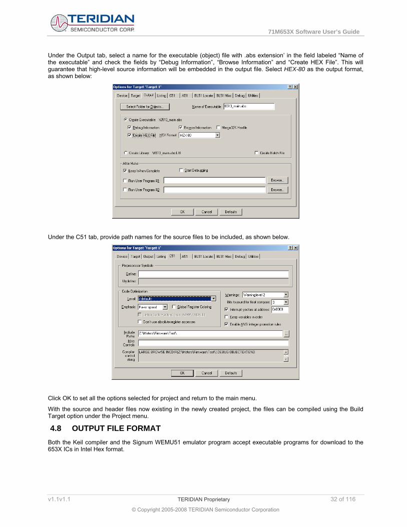
Under the Output tab, select a name for the executable (object) file with .abs extension’ in the field labeled “Name of the executable” and check the fields by “Debug Information”, “Browse Information” and “Create HEX File”. This will guarantee that high-level source information will be embedded in the output file. Select HEX-80 as the output format, as shown below:
Under the C51 tab, provide path names for the source files to be included, as shown below.
Click OK to set all the options selected for project and return to the main menu.
With the source and header files now existing in the newly created project, the files can be compiled using the Build Target option under the Project menu.
4.8 OUTPUT FILE FORMAT Both the Keil compiler and the Signum WEMU51 emulator program accept executable programs for download to the 653X ICs in Intel Hex format.
v1.1v1.1 TERIDIAN Proprietary 32 of 116
© Copyright 2005-2008 TERIDIAN Semiconductor Corporation

71M653X Software User’s Guide
4.8.1 Basic Intel Hex Format
The Intel HEX file is an ASCII text file with lines of text that follow the Intel HEX file format. Each line in an Intel HEX file contains one HEX record. These records are made up of hexadecimal numbers that represent machine language code and/or constant data. Intel HEX files are often used to transfer the program and data that would be stored in a ROM or EPROM. Most EPROM programmers or emulators can use Intel HEX files.
Record Format
An Intel HEX file is composed of any number of HEX records. Each record is made up of five fields that are arranged in the following format:
:llaaaatt[dd...]cc
Each group of letters corresponds to a different field, and each letter represents a single hexadecimal digit. Each field is composed of at least two hexadecimal digits-which make up a byte-as described below:
: is the colon that starts every Intel HEX record. ll is the record-length field that represents the number of data bytes (dd) in the record. aaaa is the address field that represents the starting address for subsequent data in the record. tt is the field that represents the HEX record type, which may be one of the following:
00 - data record 01 - end-of-file record 02 - extended segment address record 04 - extended linear address record
dd is a data field that represents one byte of data. A record may have multiple data bytes. The number of data bytes in the record must match the number specified by the ll field.
cc is the checksum field that represents the checksum of the record. The checksum is calculated by summing the values of all hexadecimal digit pairs in the record modulo 256 and taking the two's complement.
Data Records
The Intel HEX file is made up of any number of data records that are terminated with a carriage return and a linefeed. Data records appear as follows: :10246200464C5549442050524F46494C4500464C33
This record is decoded as follows:
:10246200464C5549442050524F46494C4500464C33 ||||||||||| CC->Checksum |||||||||DD->Data |||||||TT->Record Type |||AAAA->Address |LL->Record Length :->Colon
where:
10 is the number of data bytes in the record. 2462 is the address where the data are to be located in memory. 00 is the record type 00 (a data record). 464C...464C is the data. 33 is the checksum of the record.
v1.1v1.1 TERIDIAN Proprietary 33 of 116
© Copyright 2005-2008 TERIDIAN Semiconductor Corporation

71M653X Software User’s Guide
4.8.2 Intel Hex386 File Format
For banked code, the Intel Hex386 file format (Extended Linear Address Records) is used:
Extended linear address records are also known as 32-bit address records and HEX386 records. These records contain the upper 16 bits (bits 16-31) of the data address. The extended linear address record always has two data bytes and appears as follows:
:02000004FFFFFC
where:
02 is the number of data bytes in the record. 0000 is the address field. For the extended linear address record, this field is always 0000. 04 is the record type 04 (an extended linear address record). FFFF is the upper 16 bits of the address. FC is the checksum of the record and is calculated as
01h + NOT(02h + 00h + 00h + 04h + FFh + FFh).
When an extended linear address record is read, the extended linear address stored in the data field is saved and is applied to subsequent records read from the Intel HEX file. The linear address remains effective until changed by another extended address record.
The absolute-memory address of a data record is obtained by adding the address field in the record to the shifted address data from the extended linear address record. The following example illustrates this process:
Address from the data record's address field 2462 Extended linear address record data field FFFF -------- Absolute-memory address FFFF2462
v1.1v1.1 TERIDIAN Proprietary 34 of 116
© Copyright 2005-2008 TERIDIAN Semiconductor Corporation

71M653X Software User’s Guide
4.9 WRITING BANK-SWITCHED CODE The 80515 microcontroller contained in the 71M653X Energy Meter chips can only address 64Kbytes of code. This section explains how to design firmware with more than 64K of code for the 71M653X Energy Meter chips.
4.9.1 Hardware Overview
In the 71M6531 there is a 32K area from code address 0x0000 to 0x7FFF. The code in this area is always available to the 8051. This area is “common” and is the same memory area as “bank 0”. Since it is always present, it never needs to be switched into the bank area.
A 32K bank is selected by writing the bank’s number in the register FL_BANK, an SFR at 0xB6. After this, the bank’s code is visible to the MPU in addresses 0x8000 to 0xFFFF.
The 71M6531 has four 32K banks (128K bytes total). Bank 0 is the common area. Banks 1, 2, and 3 are the banked code areas selected by FL_BANK.
The 71M6534 has eight 32K banks (256K total). Bank 0 is the common area. Banks 1 through 7 are the banked code areas selected by FL_BANK.
A reset sets FL_BANK to 1, so any 71M653x IC can run 64K of non-bank-switching code.
The 71M653x ICs have two write protect registers to protect ranges at the beginning and end of flash.
The beginning is protected by BOOT_SIZE, XDATA 0x20A7 when WRPROT_BT is set in FLSHCTL, SFR 0xB2.
The end can be protected by placing the CE program at the start of the area to protect, and setting WRPROT_CE in FLSHCTL, SFR 0xB2.
FL_BANK [2:0]
Address Range for Lower Bank (Common)
(0x000-0x7FFF)
Address Range for Upper Bank
(0x8000-0xFFFF)
6531 128KB
6533 128KB
6534 256KB
000 0x0000-0x7FFF 0x0000-0x7FFF X X X 001 0x0000-0x7FFF 0x8000-0xFFFF X X X 010 0x0000-0x7FFF 0x10000-0x17FFF X X X 011 0x0000-0x7FFF 0x18000-0x1FFFF X X X 100 0x0000-0x7FFF 0x20000-0x27000 X 101 0x0000-0x7FFF 0x28000-0x2FFFF X 110 0x0000-0x7FFF 0x30000-0x37FFF X 111 0x0000-0x7FFF 0x38000-0x3FFFF X
Table 4-1: Code Bank Memory Addresses and Availability
The 71M653x ICs’ flash memory are very similar to the ROM arrangement in Keil’s example “Banking With Common Area” of chapter 9 (linker) of Keil’s “Macro assembler and Utilities” manual.
4.9.2 Software Overview
Teridian’s demonstration code uses the Keil compiler’s standard bank switching system (www.Keil.com).
This is completely supported by Keil, a major compiler vendor for 8051s, and Signum, the emulator vendor. Code can be ported from non-banked projects, and full symbolic banked debugging is available.
Keil’s scheme puts a “page table” in common memory. Code calls an entry in the page table. Each entry is a bit of code that switches to the subroutine’s bank, and jumps to the subroutine in the bank.
Keil’s linker automatically produces the page table. In Teridian’s demo code, the size of this table is less than 1K.
Code using the page table is slower than native 16-bit code, because it has to set the page register.
v1.1v1.1 TERIDIAN Proprietary 35 of 116
© Copyright 2005-2008 TERIDIAN Semiconductor Corporation

71M653X Software User’s Guide
Interrupts must start in the common (non-banked) area, because the bank register could have any value.
Calls via function pointers (e.g. “callback routines”) are supported, but need to be made global, and mapped to their caller with the linker’s overlay functions. Keil’s linker often omits callback routines from the page table when it optimizes the page table, and this causes incorrect operation.
Constant values have to be accessed from the same bank, or common code. When accessed from common code the bank has to be switched manually with switchbank(), a subroutine in the bank logic.
4.9.3 Software Tool Versions
The development software used with these examples was Keil C version 8.03, with the BL51 linker (the Lx51 linker is actually easier to use, but not shown). The Signum emulator software used was version 3.11.04.
4.9.4 Setup of the Compiler Project
This dialogue is for the project options of a 71M6531, which has 4 banks (see Figure 4-1).
Figure 4-1, Setup of Keil Compiler for bank-switched code
When opening individual files by right-clicking on the file names (after opening the group folders listed under “Target”) , file options can be edited. These options can be set to assign code to pages (as shown in Figure 4-2, ).
v1.1v1.1 TERIDIAN Proprietary 36 of 116
© Copyright 2005-2008 TERIDIAN Semiconductor Corporation

71M653X Software User’s Guide
Figure 4-2, Selecting a Bank for a File Group in Keil C
4.9.5 Startup
TSC provides special start-up code on the CD-ROMs shipped with the 71M653X Demo Kits. The code can be found at Util\startup_30_banked.a51. This file sets up the bank-switching logic. It must be included in the build. Any other startup.a51 file must be removed.
4.9.6 Bank-Switching Code
TSC has already ported Keil’s bank-switching code, Util\L51_bank.a51. TSC’s version of this file should be included in the build. TSC has already selected the fastest standard bank-switching method as the default.
During performance testing, TSC made a good-faith attempt to port the other bank-switching methods in this code, including features needed by Keil’s advanced Lx51 linker. However these versions are not extensively tested.
4.9.7 Page Table Setup and Debug
Keil’s linkers produce the page table automatically, once paging is selected in the Microvision options->target dialogue. Keil usually places the page table at an address of 0x100 in the common bank. It is visible in the linker .m51 file. To see how it works, one can use the emulator to single-step through at a banked function call at the assembly language level.
To call a paged subroutine, Keil’s linker arranges to call one of the entries of the page table. The page table consists of one entry per subroutine. Each entry is a small piece of code that loads the address of the banked subroutine into the 8051 register DPTR, and then jumps to paging code. The paging code sets the bank register FL_BANK, and then jumps to the banked code’s address contained in the DPTR.
v1.1v1.1 TERIDIAN Proprietary 37 of 116
© Copyright 2005-2008 TERIDIAN Semiconductor Corporation
71M653X Software User’s Guide
Keil’s linkers minimize the size of the page table. A subroutine has an entry in the page table only if:
1. The subroutine is in a bank, and
2. The subroutine is called from outside its bank.
Most problems with banking code occur because the linker omits a function from the page table. The result is that the call to a function in a different bank goes to code in the current bank, causing unexpected code in the current bank to be executed.
One major cause of this is a callback subroutine called via a function pointer. Another is an interrupt defined in banked assembly language file (fortunately, Keil detects and flags banked interrupts in C code).
To solve problems stemming from callback routines, all subroutines called from other banks should be made global, so that the linker can use their data.
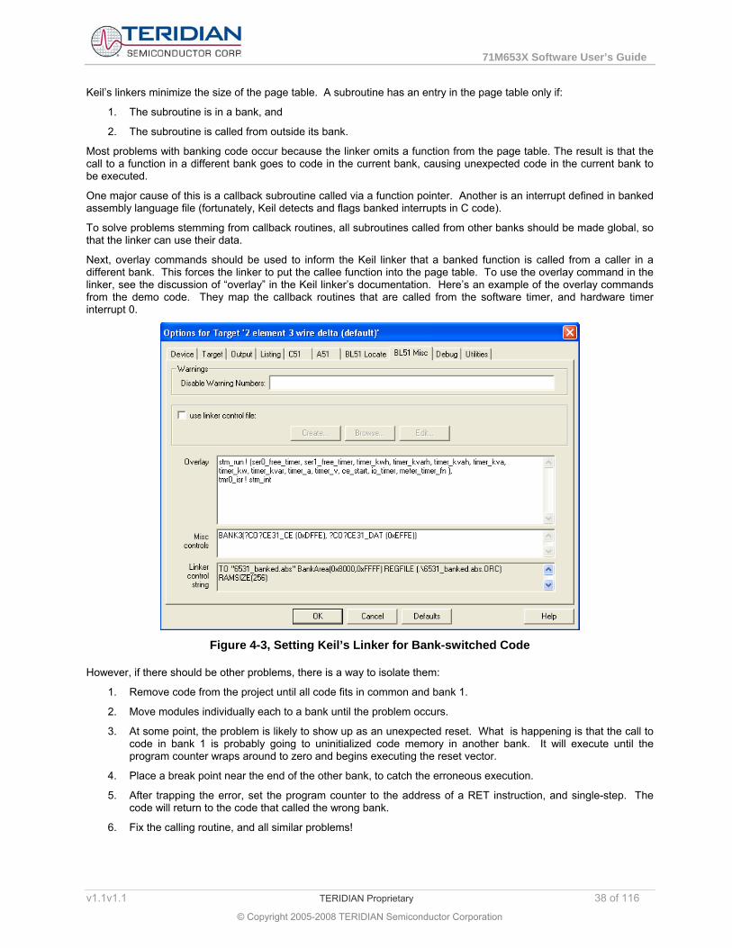
Next, overlay commands should be used to inform the Keil linker that a banked function is called from a caller in a different bank. This forces the linker to put the callee function into the page table. To use the overlay command in the linker, see the discussion of “overlay” in the Keil linker’s documentation. Here’s an example of the overlay commands from the demo code. They map the callback routines that are called from the software timer, and hardware timer interrupt 0.
Figure 4-3, Setting Keil’s Linker for Bank-switched Code
However, if there should be other problems, there is a way to isolate them:
1. Remove code from the project until all code fits in common and bank 1.
2. Move modules individually each to a bank until the problem occurs.
3. At some point, the problem is likely to show up as an unexpected reset. What is happening is that the call to code in bank 1 is probably going to uninitialized code memory in another bank. It will execute until the program counter wraps around to zero and begins executing the reset vector.
4. Place a break point near the end of the other bank, to catch the erroneous execution.
5. After trapping the error, set the program counter to the address of a RET instruction, and single-step. The code will return to the code that called the wrong bank.
6. Fix the calling routine, and all similar problems!
v1.1v1.1 TERIDIAN Proprietary 38 of 116
© Copyright 2005-2008 TERIDIAN Semiconductor Corporation
71M653X Software User’s Guide
4.9.8 Producing a Banked Hex File
The BL51 linker and its associated hex converter produce a separate Intel hex file for each bank. These files end with names such as .H01 for bank 1, .H02 for bank 2, etc. The emulator and the production programmer expect a single Intel 386 hex file with a .HEX ending.
TSC’s demo CD ROM has a utility called bank_merge.exe. It runs in a DOS command window and merges the bank files from Keil’s hex converter into one Intel-386 hex file. This can be placed in the build automatically. (how?)
Another manual solution is to erase the flash, load the .abs file to an emulator, and then use the file->save range: All menu selection to save a copy of flash as an Intel hex file.
When using Keil’s Lx51 advanced linker, the output dialog contains a pull-down list of hex formats. Select the “i386” hex file option.
The emulator’s verification option is a convenient way to verify that the .abs and .hex file have the same content. To use it, invoke the menu File->Load, then check the verify box, but not the load box.
4.9.9 Placing Interrupts in Banked Code
The interrupts must start in the common code. TSC starts most interrupts from a “trampoline” routine that saves and restores the bank register. The demo code’s trampoline routines are in Meter\io653x.c, with the stub interrupts and decoded interrupts. An example of a trampoline is this serial interrupt from Meter\io653x.c, used to service UART0:
#pragma save
#pragma REGISTERBANK (ES0_BANK)
void es0_trampoline (void) small reentrant interrupt ES0_IV using ES0_BANK
{
uint8_t my_fl_bank = FL_BANK; // save the bank register
FL_BANK = BANK_DEFAULT; // BANK_DEFAULT is 1
es0_isr();
FL_BANK = my_fl_bank; // restore the bank register
}
#pragma restore
This is clumsy and slow. Why do this?
A trampoline lets most interrupt code be in bank-switched code space with other code from the same file. This may make the code easier to read. It also leaves more space in common memory, and permits a larger system to exist. The penalty is a few tens of microseconds per interrupt.
Very frequent interrupts should not use trampoline routines. In TSC’s demo code, the CE code, Meter\ce.c has an interrupt that runs every 396 microseconds (ce_busy_isr()). ce.c is placed in the common area, and ce_busy’s trampoline is disabled (in Meter\io653x.c).
If an interrupt calls code in a bank, as above, it must save and restore the bank-switching register, FL_BANK.
Keil’s Lx51 advanced linker has an option to automatically save and restore the bank register in an interrupt. TSC’s L51_bank.a51 code provides the necessary symbols.
4.9.10 Calling Banked Functions via Function Pointers
In a banking system, functions placed in function pointers cannot have the word “static” in front of their definition. They must be global.
Also, the linker must be informed of the actual caller of the function in the function pointers. For example, in the TERIDIAN Demo Code, the software timer module (Util\stm.c) calls many routines. There is also an interrupt for hardware timer 1 that calls the software timer’s interrupt code. This linker dialogue tells the linker the true relationship. The command to the linker is “caller ! callee” or “caller ! (callee_1, callee_2, …)” (See the linker command figure, 0-3).
Why do this? If a function pointer points at a function’s entry in the page table, the function pointer can be executed from any bank, at any time. So, in theory, function pointers are supported via the page table.
v1.1v1.1 TERIDIAN Proprietary 39 of 116
© Copyright 2005-2008 TERIDIAN Semiconductor Corporation

71M653X Software User’s Guide
In practice, the Keil linker tries to save space in the page table. So, it only puts global functions into the page table if they are in a bank area and are called from outside the bank. Often, function pointers are used for callback routines. In these cases, the linker often does not detect the true caller and so cannot detect the cross-bank function call. Then, it places a banked address into the code that sets the function pointer. If this is executed from another bank, the code jumps to code in the current, wrong bank!
Using overlay commands informs the linker of the actual caller, so it can detect cross-bank calls.
To increase reliability, the demo code that sets a function pointer also checks to make sure that the pointer is in common memory rather than a bank. The code looks like this:
if (((uint16_t)fn_ptr) > 0x7FFF) // only accept functions in common
{
main_software_error (); // report a software error at a central breakpoint.
return NULL; // indicate a failure to the caller
}
4.9.11 Putting Constants in Banks
Space in the common code area can be precious. It often helps to put large tables in a different code bank. The TERIDIAN Demo Code, places the help text, CE code and the CE’s data initialization table into banked flash.
In order for this to work, every reference to the data must be from the same bank or from common.
In the demo code, the largest set of constant tables is the help text. The help text (CLI\Help.c) is in the same bank as the printing routines, which copy the text into RAM for use by the serial interrupts (see CLI\io.c). Since the help text is in the same bank as the accessing routines, no other special coding is needed.
In the demo code, the CE code is referenced from the Meter\ce.c. ce.c could not be placed in the last bank with the tables because it also has a very fast interrupt, ce_busy_isr(), so ce.c was placed in common. Also, the CE code is in the last bank, so the code in ce.c had to explicitly switch it in to read it.
Designers must be careful that any code in common is smaller than the data table! Some systems may need a library routine in common to copy part of the banked data to RAM for use by banked code.
Next, the data should be located in the desired bank, using compiler and linker’s BANK commands. (See the compiler and linker command figures, 0-2, 0-3)
The code using the banked data should include Util\bank.h, which defines switchbank() to access banked data.In the code that accesses the data, the bank must be switched in. For example, when the demo code copies the starting data for the CE (ce_init() in Meter\ce.c), it executes the following code:
switchbank (BANK_CE);
memcpy_cer (
(int32x_t *)CE_DATA_BASE,
(int32r_t *)&CeData[0],
(uint8_t)(0xff & NumCeData)
);
switchbank () sets the bank register without side effects for other bank switching. It is defined in Util\bank.h. BANK_CE is the bank number containing the CE initialization table (in Main_6531\options.h or Main_6534\Options.h). memcpy_cer () copies 32-bit words from code to CE memory. CE_DATA_BASE is the start of CE memory, 0x0000 in XDATA in 71M653x ICs. CeData[] is the array of 32-bit integers containing the CE’s default data. NumCeData is the count of data words in the table, a constant value that precedes the CE default data table.
4.9.12 Write-Protecting Flash in the 653X
Besides safety interlocks in software that prevent accidental write operations to flash, the 71M653x ICs also have a write-protection mechanism implemented in hardware. Some systems might permit code or customization tables to be downloaded to flash, and designers might wish to assure that this process cannot corrupt other code or data.
v1.1v1.1 TERIDIAN Proprietary 40 of 116
© Copyright 2005-2008 TERIDIAN Semiconductor Corporation

71M653X Software User’s Guide
To protect flash starting at address 0x00000, write the number of 1,024-byte blocks into BOOT_SIZE (at XDATA 0x20A7), and set WRPROT_BT (bit 5 of SFR 0xB2). Since this range covers the code’s interrupt vectors, it is perfect for protecting a boot loader (i.e. code that can load other code into the system). It is also the logical choice for general-purpose write-protection.
To protect flash near the end of memory, place the CE’s data area at that point (and set CE_LCTN, XDATA 0x20A8), and set the WRPROT_CE (bit 4 of SFR 0xB2). This protects not only the CE code, but also all flash memory after it. This is excellent for protecting the CE code and calibration tables stored in flash. The demo code uses this method to protect the CE code and its default initialization table.
4.10 PROJECT MANAGEMENT TOOLS With large software projects involving a multitude of source, object, list and other files in various revisions, it is very helpful to use a version control tool.
To manage file versions under Windows, Tortoise CVS, a free version control utility, might be useful. This utility can be found at http://www.tortoisecvs.org/ .
4.11 ALTERNATIVE COMPILERS The Demo Code was written for the Keil compiler. However, alternative compilers may be used if the code is modified to ensure compatibility with the alternative compiler. One example of an alternative compiler is SDCC, a free compiler available from www. Sourceforge.net.
Note: The Keil extensions for the 8051 are not compatible with the 8051 extensions used by the SDCC.
The batch file BUILD653X.BAT is provided with the Demo Kit to support building object files using alternative compilers. This batch file uses the Keil compiler calls with the applicable compiler options and can therefore serve as examples on how to invoke alternative compilers. The linker control file LINK653x.TXT called by the batch files can show how to properly invoke linkers.
To compile with DOS-style tools, arrange for a DOS batch file to invoke the tools and set the properties of the batch file to leave the window open, so that errors can be seen. Then, to compile, double click on this batch file in Windows explorer.
4.12 ALTERNATIVE EDITORS Many modern text editors have a feature called “tag jumping” that helps a programmer to read and understand unfa-miliar code. TERIDIAN Semiconductor recommends using such an editor to read, understand and modify demonstration code. Tag jumping is a feature that is not supported by the Keil uVision editor.
This is how tag jumping works:
1. A “tag file generator” program is run on some directories full of .c or .h files. TERIDIAN Semiconductor recommends placing the tag file generator in a DOS batch file in the same directory as the project’s make file. Wattmeter demonstration code includes such a batch file: “T.BAT”. To run a batch file, double-click it in windows explorer. A DOS batch file is just an ASCII file (like a .C file) containing DOS commands. DOS commands are described at http://www.computerhope.com/msdos.htm .
2. The tag file should then be copied to convenient places for a text editor. TERIDIAN Semiconductor recommends copying the tag file into each source code directory. In that way, the default tag file location for most editors becomes just “.\tags” for all projects, and multiple projects do not conflict. Copying the tag file can be an automatic part of the DOS batch file that generates the tag file.
3. It is easiest if Windows explorer opens .C files automatically with the editor when they are clicked. To do this, change file associations. (See Windows help.)
4. Inside the editor, select a subroutine name or variable, then use the editor’s “tag jump” feature. The editor immediately opens the file at the line where the subroutine or variable is defined. Or, if the same symbol is in several places, it offers a choice of files.
TERIDIAN Semiconductor recommends the “exuberant CTAGs utility” for generating tag files. The code can be found for free at: http://ctags.sourceforge.net/. The choice of a text editor is very personal. Many editors support Exuberant CTAGS. See the list of supporting tools at http://ctags.sourceforge.net/tools.html.
v1.1v1.1 TERIDIAN Proprietary 41 of 116
© Copyright 2005-2008 TERIDIAN Semiconductor Corporation

71M653X Software User’s Guide
Some editors to be considered are:
• VIM, see http://www.vim.org/ a free VI editor. VIM is available in full-featured versions for Windows. VI is part of the POSIX standard, so using it is a portable skill. VIM wins awards for usability.
• UltraEdit http://www.ultraedit.com/ , an inexpensive (not free), professional Windows programming editor. This editor works like all other Windows applications, with extra features to support programming languages. NEDIT (The Nirvana Editor) is very similar, at http://www.nedit.org/. NEDIT runs on Unix with Motif, and also supports exuberant CTAGs.
• GNU Emacs, a free editor, also supports exuberant CTAGs. See: http://www.gnu.org/software/emacs/emacs.html
4.13 ALTERNATIVE LINKERS Compiled and linked code can be significantly compacted by using the linker available with the Professional Compiler Kit PK51 from Keil (www.keil.com).
The LX51 Enhanced Linker supplied with the PK51 kit (http://www.keil.com/c51/lx51.asp) is capable of code compression by up to 8% by rearranging code segments for AJMP and ACALL usage.
All executables supplied with the Demo Boards were generated using the conventional compilers and linkers from Keil. That way, the supplied sources compile and link to the same code size as the pre-compiled object files.
If it is desired to add more options to the source code than the BL51 linker can pack into a given code space, the LX51 Enhanced Linker should be considered.
v1.1v1.1 TERIDIAN Proprietary 42 of 116
© Copyright 2005-2008 TERIDIAN Semiconductor Corporation

71M653X Software User’s Guide
5 5 DEMO CODE DESCRIPTION
5.1 80515 DATA TYPES AND COMPILER-SPECIFIC INFORMATION
5.1.1 Data Types
The 80515 MPU core is an 8-bit micro controller (MPU); thus operations that use 8-bit data types such as “char” or “unsigned char” work more efficiently than operations that use multi-byte types, such as “int” or “long”. The Keil C51 compiler supports ANSI C data types as well as data types that are unique to the generic 8051 controller family. Table 5-2 lists available data types. Please refer to the Keil Cx51 Compiler User’s Guide for more details.
Various types of address spaces are available for the 80515 MPU core of the 71M653X, and in order to utilize the various memory space types efficiently, the Demo Code uses variable type definitions (typedefs.) presented in this chapter.
To understand the data types, it helps to examine the internal data memory map of the 80515 MPU core, as shown in Table 5-1: .
Address Direct addressing Indirect addressing 0xFF Special Function Registers
(SFRs) RAM 0x80 0x7F
Byte-addressable area 0x30 0x2F
Bit-addressable area 0x20 0x1F
Register banks R0…R7 0x00
Table 5-1: Internal Data Memory Map
v1.1v1.1 TERIDIAN Proprietary 43 of 116
© Copyright 2005-2008 TERIDIAN Semiconductor Corporation

71M653X Software User’s Guide
The demo software defines standard integers in util\stdint.h following the industry-standard notation.
General data type definitions:
typedef unsigned char uint8_t; // an 8-bit byte, unsigned
typedef unsigned short uint16_t; // a 16-bit unsigned integer
typedef unsigned long uint32_t; // a 32-bit unsigned integer
typedef signed char int8_t; // a signed 8-bit integer
typedef signed short int16_t; // a signed 16-bit integer
typedef signed long int32_t; // a signed 32-bit integer
Type definitions for internal data, lower 128 bytes, addressed directly:
typedef unsigned char data uint8d_t;
typedef unsigned short data uint16d_t;
typedef unsigned long data uint32d_t;
typedef signed char data int8d_t;
typedef signed short data int16d_t;
typedef signed long data int32d_t;
Internal data is the fastest available memory (except registers), not battery-backed-up, but competes with stack, registers, booleans, and idata for space.
Note: For portability, see uint_fast8_t and its sisters, which are POSIX standard.
Type definitions for internal data, 16 bytes (0x20 to0x2F), addressed directly, and bit addressable:
typedef unsigned char bdata uint8b_t;
typedef unsigned short bdata uint16b_t;
typedef unsigned long bdata uint32b_t;
typedef signed char bdata int8b_t;
typedef signed short bdata int16b_t;
typedef signed long bdata int32b_t;
Bit addressable memory is the fastest available memory, but it is not battery-backed-up. It competes with stack, registers, bools, data, and idata for space. The space is valuable for boolean globals and should not be wasted.
Booleans are not a normal part of stdint.h, but they are fairly portable. When using the Keil compiler, the Booleans are stored in the address range 0x20 to 0x2F. Keil functions return bools in the carry bit, which makes code that's fast and small.
typedef bit bool;
#define TRUE 1
#define FALSE 0
#define ON 1
#define OFF 0
v1.1v1.1 TERIDIAN Proprietary 44 of 116
© Copyright 2005-2008 TERIDIAN Semiconductor Corporation

71M653X Software User’s Guide
Type definitions for internal data, 256 bytes, in the upper 128 bytes addressed indirectly:
typedef unsigned char idata uint8i_t;
typedef unsigned short idata uint16i_t;
typedef unsigned long idata uint32i_t;
typedef signed char idata int8i_t;
typedef signed short idata int16i_t;
typedef signed long idata int32i_t;
Indirectly addressed internal memory is fairly fast, not battery-backed-up, slower than the data in the lower 128 bytes of internal memory. Competes with data for space.
Type definitions for external data, 256 bytes of 2K of CMOS RAM:
typedef unsigned char pdata uint8p_t;
typedef unsigned short pdata uint16p_t;
typedef unsigned long pdata uint32p_t;
typedef signed char pdata int8p_t;
typedef signed short pdata int16p_t;
typedef signed long pdata int32p_t;
The upper byte of the XDATA address is supplied by the SFR 0xBF (ADRMSB or USERP) on the 71M653x meter ICs. On other 8051 processors, P2 is used for this purpose. This memory range is accessed indirectly, still fairly fast, not battery backed-up. This is a logical place for nonvolatile globals like power registers and configuration data.
Type definitions for external data, 2Kbytes of CMOS RAM, accessed indirectly via a 16-bit register:
This is the slowest but largest memory area, not battery backed-up. It can be used for everything possible. On Keil's large memory model, this is the default.
typedef unsigned char xdata uint8x_t;
typedef unsigned short xdata uint16x_t;
typedef unsigned long xdata uint32x_t;
typedef signed char xdata int8x_t;
typedef signed short xdata int16x_t;
typedef signed long xdata int32x_t;
Type definitions for external read-only data, located in code space:
typedef unsigned char code uint8r_t;
typedef unsigned short code uint16r_t;
typedef unsigned long code uint32r_t;
typedef signed char code int8r_t;
typedef signed short code int16r_t;
typedef signed long code int32r_t;
Access is indirect via a 16-bit register. This is the slowest but largest space, nonvolatile programmable flash memory. It should be used for constants and tables. If the table is in banked space, the banking function switchbank() (defined in utils\bank.h and L51_BANK.A51) may be needed to bring the code bank into the address space.
v1.1v1.1 TERIDIAN Proprietary 45 of 116
© Copyright 2005-2008 TERIDIAN Semiconductor Corporation
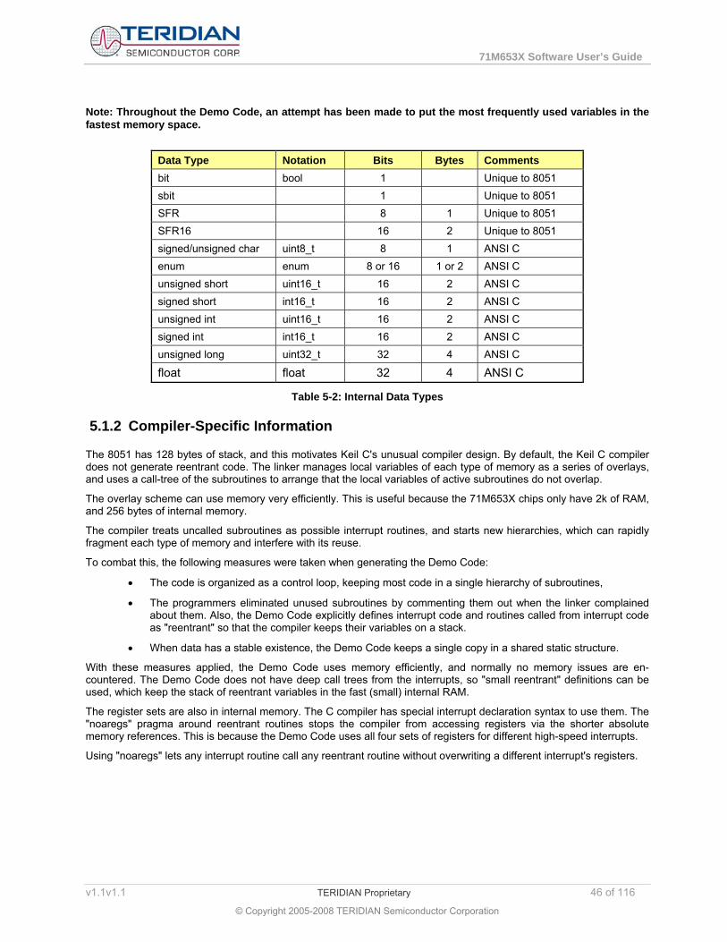
71M653X Software User’s Guide
Note: Throughout the Demo Code, an attempt has been made to put the most frequently used variables in the fastest memory space.
Data Type Notation Bits Bytes Comments bit bool 1 Unique to 8051 sbit 1 Unique to 8051 SFR 8 1 Unique to 8051 SFR16 16 2 Unique to 8051 signed/unsigned char uint8_t 8 1 ANSI C enum enum 8 or 16 1 or 2 ANSI C unsigned short uint16_t 16 2 ANSI C signed short int16_t 16 2 ANSI C unsigned int uint16_t 16 2 ANSI C signed int int16_t 16 2 ANSI C unsigned long uint32_t 32 4 ANSI C
float float 32 4 ANSI C
Table 5-2: Internal Data Types
5.1.2 Compiler-Specific Information
The 8051 has 128 bytes of stack, and this motivates Keil C's unusual compiler design. By default, the Keil C compiler does not generate reentrant code. The linker manages local variables of each type of memory as a series of overlays, and uses a call-tree of the subroutines to arrange that the local variables of active subroutines do not overlap.
The overlay scheme can use memory very efficiently. This is useful because the 71M653X chips only have 2k of RAM, and 256 bytes of internal memory.
The compiler treats uncalled subroutines as possible interrupt routines, and starts new hierarchies, which can rapidly fragment each type of memory and interfere with its reuse.
To combat this, the following measures were taken when generating the Demo Code:
• The code is organized as a control loop, keeping most code in a single hierarchy of subroutines,
• The programmers eliminated unused subroutines by commenting them out when the linker complained about them. Also, the Demo Code explicitly defines interrupt code and routines called from interrupt code as "reentrant" so that the compiler keeps their variables on a stack.
• When data has a stable existence, the Demo Code keeps a single copy in a shared static structure.
With these measures applied, the Demo Code uses memory efficiently, and normally no memory issues are en-countered. The Demo Code does not have deep call trees from the interrupts, so "small reentrant" definitions can be used, which keep the stack of reentrant variables in the fast (small) internal RAM.
The register sets are also in internal memory. The C compiler has special interrupt declaration syntax to use them. The "noaregs" pragma around reentrant routines stops the compiler from accessing registers via the shorter absolute memory references. This is because the Demo Code uses all four sets of registers for different high-speed interrupts.
Using "noaregs" lets any interrupt routine call any reentrant routine without overwriting a different interrupt's registers.
v1.1v1.1 TERIDIAN Proprietary 46 of 116
© Copyright 2005-2008 TERIDIAN Semiconductor Corporation

71M653X Software User’s Guide
There is a known defect in version 7.50a of the Keil compiler:
Memory types must be explicitly defined in local variables. Using a predefined type is not explicit enough, i.e. "char xdata c;" is ok. "typedef char int8_t; ... int8_t data c;" is OK,
but "typedef char data int8d_t; ... int8d_t c;" is not OK.
5.2 DEMO CODE OPTIONS AND PROGRAM SIZE Since the 71M6531 is single phase, and the 71M6534 is tree-phase, different versions of the Demo Code are provided that take into account the different features (see Table 5-3). An attempt has been made to provide the most common features in each version of the Demo Code. Flexibility is provided by the source code for users when recompiling the source code: If a certain feature is not required, it can be left out and replaced with a different feature.
The object files contained in the Demo Kits have been generated with the following Keil compiler versions: • C compiler: C51.exe, V8.05a • Assembler: A51.exe, V8.00b • Linker/Locator: BL51.exe, V6.05 • Librarian: LIB51.exe, V4.24 • Hex-converter: OH51.exe, V2.6
Version Flash Code Size Description
Single Phase ~45KB Demonstrates a single phase meter. The software offers calibration and nonvolatile energy registers. It utilizes one set of CE code for 1 element two wire meters, and another set for 1 element three wire, and 2 element three wire delta.
Three Phase ~49KB Demonstrates a three-phase meter. The software is easy to reconfigure by recompiling. It has calibration and nonvolatile energy registers. The software demonstrates a full feature set.
Table 5-3: Demo Code Versions
In addition to providing flexibility, an attempt has been made to leave a certain amount of unoccupied memory space when generating the Demo Code. This should provide some room for users who want to modify the Demo Code and experiment with small changes.
The tables presented below show the features available for the three versions of the Demo Code plus the code size required for each feature. Entries for code size are approximated and depend on code module combination.
Y means that the feature is implemented, N means that it is not. N/opt means that the feature may be implemented if enough memory space is available.
Feature Code
Size 1φ 3φ Description
CT and shunt resistors
1KB to 2.5KB
Y Y Configurations include all 2 element 3 wire delta, and 3 element 4 wire wye with neutral current. These were selected for demonstration because they permit easy measurements of individual elements.
Rogowski coils 2.5KB N N Needs special CE code; contact factory
Table 5-4: Current Sensing Options
v1.1v1.1 TERIDIAN Proprietary 47 of 116
© Copyright 2005-2008 TERIDIAN Semiconductor Corporation
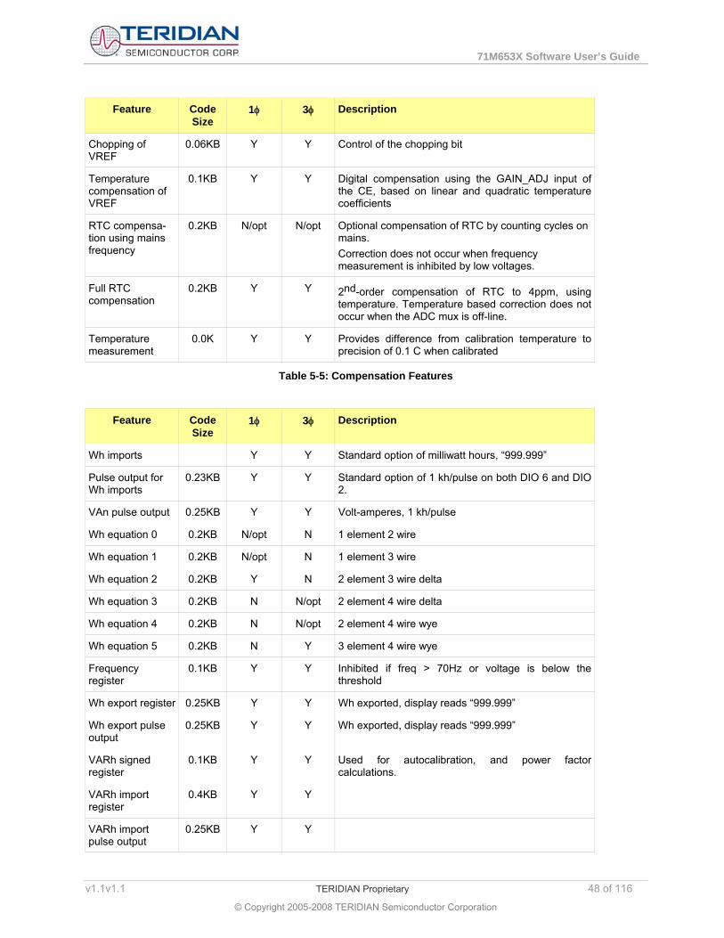
71M653X Software User’s Guide
Feature Code
Size 1φ 3φ Description
Chopping of VREF
0.06KB Y Y Control of the chopping bit
Temperature compensation of VREF
0.1KB Y Y Digital compensation using the GAIN_ADJ input of the CE, based on linear and quadratic temperature coefficients
RTC compensa-tion using mains frequency
0.2KB N/opt N/opt Optional compensation of RTC by counting cycles on mains. Correction does not occur when frequency measurement is inhibited by low voltages.
Full RTC compensation
0.2KB Y Y 2nd-order compensation of RTC to 4ppm, using temperature. Temperature based correction does not occur when the ADC mux is off-line.
Temperature measurement
0.0K Y Y Provides difference from calibration temperature to precision of 0.1 C when calibrated
Table 5-5: Compensation Features
Code Size
1φ 3φ Description Feature
Wh imports Y Y Standard option of milliwatt hours, “999.999”
Pulse output for Wh imports
0.23KB Y Y Standard option of 1 kh/pulse on both DIO 6 and DIO 2.
VAn pulse output 0.25KB Y Y Volt-amperes, 1 kh/pulse
Wh equation 0 0.2KB N/opt N 1 element 2 wire
Wh equation 1 0.2KB N/opt N 1 element 3 wire
Wh equation 2 0.2KB Y N 2 element 3 wire delta
Wh equation 3 0.2KB N N/opt 2 element 4 wire delta
Wh equation 4 0.2KB N N/opt 2 element 4 wire wye
Wh equation 5 0.2KB N Y 3 element 4 wire wye
Frequency register
0.1KB Y Y Inhibited if freq > 70Hz or voltage is below the threshold
Wh export register 0.25KB Y Y Wh exported, display reads “999.999”
Wh export pulse output
0.25KB Y Y Wh exported, display reads “999.999”
VARh signed register
0.1KB Y Y Used for autocalibration, and power factor calculations.
VARh import register
0.4KB Y Y
VARh import pulse output
0.25KB Y Y
v1.1v1.1 TERIDIAN Proprietary 48 of 116
© Copyright 2005-2008 TERIDIAN Semiconductor Corporation

71M653X Software User’s Guide
Code Size
1φ 3φ Description Feature
VARh export register
0.4KB Y Y
VARh export pulse output
0.25KB Y Y
Operating hours register
0.36KB Y Y “99999.9” Nonvolatile count of hundredths of hours of powered operation since first cold start.
RTC time register 0.18KB Y Y
RTC date register 0.21KB Y Y
Pulse source selection
0.4KB Y Y This is the ability to route most calculated energy values to a pulse output.
Dual IMAX registers
0.2KB Y N IMAX2 adjusts current, Wh and VARh from channel B to same units as A. Creep thresholds are required, but need not be adjusted when IMAX2 changes.
Neutral Current 0.3KB N Y This includes not just a measurement, but also a limit, and a count of overcurrent events.
RMS current register
0.2KB Y Y Implemented for all phases “000.000” Includes element currents, arithmetic sum of currents and (if supported) neutral current.
RMS voltage register
0.2KB Y Y Implemented for all elements “000.000”
Power factor register
0.3KB Y Y All phases are displayed with sign. Volatile.
Pulse count 1.2KB Y Y Both the Wh and VARh pulses are counted.
Mains edge count 0.3KB Y Y Counts total zero crossings, and zero crossings in the last accumulation interval, of element A.
Table 5-6: Power Registers and Pulse Output Features
v1.1v1.1 TERIDIAN Proprietary 49 of 116
© Copyright 2005-2008 TERIDIAN Semiconductor Corporation

71M653X Software User’s Guide
Feature
Feature Code Size
1φ 3φ Description
Creep mode 0.37KB Y Y Adjustable at calibration. If V < Vthreshold and I < Ithreshold for all elements, then creep.
Zero accumulator of CE
N/A Y Y The pulse accumulation register in the CE is cleared to prevent spurious pulses from low current noise.
Current threshold N/A Y Y Adjustable at calibration.
Set If max(abs(IA2), abs(IB2)) < Current threshold then creep mode. Current is calculated from RMS if possible, or, if below 0.1A, from VA / V, where VA is calculated as sqrt(Wh^2 + VARh^2) For all elements.
Voltage threshold 0.12KB Y Y Adjustable at calibration.
If max(abs(VA2), abs(VB2)) < Volt threshold inhibit frequency measurement, (frequency of zero) Inhibit use of zero crossing counts, (main edge count is zero), iInhibit voltage phase measurement (if any) This feature is needed only if frequency or mains edge count is present.
Table 5-7: Creep Functions
Feature Code
Size 1φ 3φ Description
Brownout mode 0.1KB Y Y Used to enter sleep and LCD modes. Command line interface is available (32KB) when resetting into this mode. Command prompt in this mode to be “B>”.
LCD mode 0.5KB Y Y Is entered automatically when power fails. Displays the Wh register, waits 7 sec using wakeup timer, then initiates sleep mode.
Wake button 0.5KB Y Y When in sleep mode, enters LCD mode.
Wake timer 0.5KB Y Y Used to exit the LCD mode, and enter sleep mode.
Table 5-8: Operating Modes
Note: The sleep mode does not require any support by MPU code. The mission mode performs the other code features.
v1.1v1.1 TERIDIAN Proprietary 50 of 116
© Copyright 2005-2008 TERIDIAN Semiconductor Corporation

71M653X Software User’s Guide
Feature
Feature Code Size
1φ 3φ Description
Reception of calibration parameters via the serial interface
2.0KB Y Y Simple serial calibration system to read and set data and calibration values, including CE data, MPU calibration and RTC settings. Meter operation is not required when this feature is in use. Intel hex records are used.
Count of calibrations since first cold reset.
01.KB Y Y Counts calibrations. 0..254, 255 = “many”. The count is protected by a checksum. The first cold reset is detected by an invalid EEPROM. This is a tamper-detection feature.
Auto-calibration 3.5KB Y Y Internal automatic calibration, from command line interface. Calibration adjusts phase, as in the “fast calibration” described in the DBUM.
Command Line Interface (CLI)
23KB Y Y Text-based commands give access to CE data, RAM, IO registers. Includes on-line help. No profile or load features..
Save registers when sag occurs
0.75KB Y Y Saves power and error registers on sag detection.
Save to flash memory
0.9KB N/opt N/opt Compilation option to save calibration, error and power register data to internal flash. When a flash area is used-up, it is marked, and the next one is used. When all areas are used up, an error is recorded and write operations are inhibited.
Save to and restore from EEPROM
0.7KB Y Y Saves and restores calibration, error and power register data to and from EEPROM. When an EEPROM area is used-up, it is marked, and the next one is used. When all areas are used up, an error is recorded and write operations are inhibited.
Checksum 0.2KB Y Y Each revenue-affecting data area is protected by a simple checksum
0.4KB Y Y Errors are recorded. Error data is protected by a checksum. The time stamp (minute, hour, day and month of assertion) and the bit number of the five most recent errors are saved.
Error recording and saving
Microwire EEPROM
0.2KB N/opt N/opt Compilation option
I2C EEPROM 0.2KB Y Y For an Atmel AT24C256.
Table 5-9: Calibration and Various Services
5.3 PROGRAM FLOW This section should be read with a PC that has demo code’s source code installed. This section is supposed to help you learn to find and change things in the demo code, not just learn theory.
So please, put the demo code sources on a PC now, and sit next to it!
v1.1v1.1 TERIDIAN Proprietary 51 of 116
© Copyright 2005-2008 TERIDIAN Semiconductor Corporation

71M653X Software User’s Guide
5.3.1 Startup and Initialization
The top-level functionality of the Demo Board is controlled by the high-level functions. The start-up code and main loop is in the main() program (in main\main.c). It performs the following steps:
1. Reset watchdog timer
2. Process the pushbutton (PB) when in BROWNOUT mode.
3. Initialize hardware, pointers, metering variables, UART buffers and pointers, CE, restoration of calibration co-efficients, initialization of LCD w/ “HELLO” message), enabling CE and pulse generators.
4. Execute the main_run() routine in an endless loop. In this loop, the background tasks, such as metering, processing of timers, etc. are performed. In this loop, if a command is waiting, the command line interface (CLI) reads it and does it.
Before the MPU gets to execute the main() program, it will execute the startup code contained in the STARTUP.A51 assembly program. This code jumps form the reset vector, at address 0x0000, to C_START, the startof the initialization code.
After disabligninterrupts, setting the security bit (if needed) and clearing memory, STARTUP.A51 jumps to C_START, in Keil’s assembly program init.A51 (in Keil/C51/LIB). Init.A51 sets up the 8051 for Keil C and jumps to main(). The startup files are described in section 5.10 .
The stack is located at 0x80, growing to higher values, while the reentrant stack is located at 0xFF, growing down-wards.
Once operating, the main() program expects regular interrupts from the CE.
The main() program calls the main_init()and the main_run() routines. main_init() initializes the meter’s hardware and software. main_run() is the main loop.
5.4 BASIC CODE ARCHITECTURE The TERIDIAN 71M653X firmware can be divided into two code parts, the main loop (or “background”), and the interrupts (or “foreground”).
The initialization and main loop takes care of the non time-critical functions. After the meter is initialized, the main loop runs all the time. The main loop is a small loop near the end of main() in main\main.c.
The main loop performs multitasking by calling a different subroutine for each major system task. The subroutines called in the main loop are usually either waiting for data, or the data is available and they can process it.
If they are waiting, they test a flag or counter and then return to the main loop, freeing the MPU to call other subroutines. The meter doesn’t have many tasks, so checking flags is much faster than putting event records in a queue and then interpreting them. (Queuing is the other common scheme.) It’s also easier to read the code.
These task routines will be discussed more below.
As much code as possible is called from the main loop. This helps the Keil linker to use less RAM when it organizes the overlays for the temporary variables. Also, code for the main loop is easier to write than interrupt code. For example, the software timers’ update routine, stm_run() (Util\stm.c) is called from the main loop (see main_background() in main\main.c) instead of a timer interrupt, because it reduces the chances that a timer routine will be called in an unexpected way at an unexpected time.
The meter has to keep running while waiting for serial input or output from the user. So, the main loop has two parts (see main_run()and main_background() in main\main.c). The serial input and output routines call main_background() to keep the meter running while waiting for serial input from or output. For example, see Serial0_CTx() in cli\ser0cli.c. main_background() calls the task subroutines needed to keep the meter running. main_run() calls the serial input and output code (e.g. the command line interface or an AMR system) in addition to calling main_background() to run the meter. Thus, no routine called from main_background() should perform serial I/O, because the serial I/O might try to call main_background() and this could cause an infinite recursion that would overflow the stack. The Keil linker automatically generates a “recursion error” if such code is written.
The second part is the interrupt-driven code (Foreground), such as the CE_BUSY Interrupt, Timer Interrupt, and other Interrupt service routines. The interrupt service routines (ISRs) get the data, and set a flag or counter to tell the background routine to stop waiting. These will be discussed more below.
v1.1v1.1 TERIDIAN Proprietary 52 of 116
© Copyright 2005-2008 TERIDIAN Semiconductor Corporation

71M653X Software User’s Guide
5.4.1 Initialization
When the power applied for the first time or RESETZ is asserted, the 71M653X device executes the code pointed to by the reset vector.
5.4.2 Interrupts
There are 13 interrupts available for the 80515, and the revision 4.4 Demo Code uses 11 interrupts. Table 5-10 shows the interrupt service routines (ISRs), the corresponding vectors (Table 6-58 in section 6.3.5.4) and their priority, as assigned by the MPU using the IP0 and IP1 registers (see section 6.3.5.2). In general, stubbed interrupts or shared interrupt code is defined in meter\io653x.c.
Interrupt Source Interrupt Service
Routine External or
Internal Interrupt
In source file Vector Priority (3 =
highest) Pulse count pcnt_w_isr() EXT0 Meter\pcnt.c 0x03 0 Pulse count pcnt_v_isr() EXT1 Meter\pcnt.c 0x13 3 Flash-Write collision fwcol0
fwcol_isr() EXT2 Meter\io653x.c 0x4B 0
Flash-Write collision fwcol1
fwcol_isr() EXT2 Meter\io653x.c 0x4B 0
CE Busy ce_busyz_int() EXT3 Meter\ce.c 0x53 3 Power fail/power return pll_isr() EXT4 Main\batmodes
.c 0x5B 3
EEPROM eeprom_isr() EXT5 IO\eeprom.c 0x63 0 XFER busy ce_xfer_busyz_isr () EXT6 (shared
w/ RTC) Meter\ce.c 0x6B 2
RTC rtc_isr() EXT6 (shared w/ XFER)
IO\rtc_30.c 0x6B 2
NEAR_OVERFLOW xfer_rtc_isr () EXT6 (shared w/ XFER)
Meter\io653x.c 0x6B 2
Timer0 tmr0_isr() IO\tmr0.c 0x0B 0 Timer1 tmr1_isr() IO\tmr1.c 0x1B 3 UART 0 es0_isr IO\serial.c 0x23 0 UART 1 es1_isr IO\serial.c 0x83 0
Table 5-10: Interrupt Service Routines
In general, a higher priority interrupt can preempt lower-priority interrupt code. The interrupt priority hardware is controlled by two registers, IP and IP1 (named IPL and IPH in the demo code). The MPU supports four priorities, and a fifth is possible with a small amount of software support.
The best practice is to set priorities once, near the start of initialization. Setting priorities dynamically while interrupts occur can have undefined results. Since some of the interrupts detect power failures that can occur at any time, changing interrupt priorities in the middle of the code is not recommended.
In the 653x demo code, interrupt priorities are set higher for urgent tasks. Among equally-urgent tasks, priorities are set higher for faster interrupts. The following describes interrupt priorities for the version 4.3.3 of the Demo Code:
The priority is set once, in main_init() of main\Main.c. It is also cleared to 0s in the soft reset routine, but this is followed by logic that calls four RTIs to reset the interrupt acknowledge logic for all four hardware interrupt levels. The system priority value is assembled from constants in Main\options_gbl.h. The constants are defined in Util\priority2x.h.
The highest priority interrupt group is the PLL_OK interrupt (external interrupt 4, see Main\batmodes.c), and timer 1. PLL_OK is urgent because it indicates power supply failure, and the software must start battery modes. Timer 1 shares the same priority bits, and is currently unused (sample code is in Io\tmr1.c, &.h), though earlier versions used it to set the real-time-clock.
v1.1v1.1 TERIDIAN Proprietary 53 of 116
© Copyright 2005-2008 TERIDIAN Semiconductor Corporation
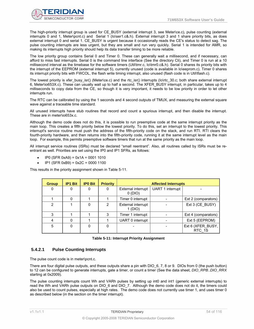
71M653X Software User’s Guide
The high-priority interrupt group is used for CE_BUSY (external interrupt 3, see Meter\ce.c), pulse counting (external interrupts 0 and 1, Meter\pcnt.c) and Serial 1 (Io\ser1.c&.h). External interrupt 3 and 1 share priority bits, as does external interrupt 0 and serial 1. CE_BUSY is urgent because it occasionally reads the CE's status to detect sag. The pulse counting interrupts are less urgent, but they are small and run very quickly. Serial 1 is intended for AMR, so making its interrupts high priority should help its data transfer timing to be more reliable.
The low priority group contains Serial 0 and Timer 0. These can generally wait a millisecond, and if necessary, can afford to miss fast interrupts. Serial 0 is the command line interface (See the directory Cli), and Timer 0 is run at a 10 millisecond interval as the timebase for the software timers (Util\tmr.c, Io\tmr0.c&.h). Serial 0 shares its priority bits with the interrupt of the EEPROM (external interrupt 5), currently unused (code is available in Io\eeprom.c). Timer 0 shares its interrupt priority bits with FWCOL, the flash write timing interrupt, also unused (flash code is in Util\flash.c).
The lowest priority is xfer_busy_isr() (Meter\ce.c) and the rtc_isr() interrupts (Io\rtc_30.c; both share external interrupt 6, Meter\io653X.c). These can usually wait up to half a second. The XFER_BUSY interrupt, in particular, takes up to 4 milliseconds to copy data from the CE, so though it is very important, it needs to be low priority in order to let other interrupts run.
The RTC can be calibrated by using the 1 seconds and 4 second outputs of TMUX, and measuring the external square wave against a traceable time standard.
All unused interrupts have stub routines that record and count a spurious interrupt, and then disable the interrupt. These are in meter\io653x.c.
Although the demo code does not do this, it is possible to run preemptive code at the same interrupt priority as the main loop. This creates a fifth priority below the lowest priority. To do this, set an interrupt to the lowest priority. This interrupt's service routine must push the address of the fifth-priority code on the stack, and run RTI. RTI clears the fourth-priority hardware, and then returns into the fifth-priority code, running it at the same interrupt level as the main loop. For example, this permits preemptive software timers that run at the same priority as the main loop.
All interrupt service routines (ISRs) must be declared “small reentrant”. Also, all routines called by ISRs must be re-entrant as well. Priorities are set using the IP0 and IP1 SFRs, as follows:
• IP0 (SFR 0xA9) = 0x1A = 0001 1010 • IP1 (SFR 0xB9) = 0x2C = 0000 1100
This results in the priority assignment shown in Table 5-11.
Group IP1 Bit IP0 Bit Priority Affected Interrupts 0 0 0 0 External interrupt
0 (DIO) UART 1 interrupt -
1 0 1 1 Timer 0 interrupt - Ext 2 (comparators)2 1 0 2 External interrupt
1 (DIO) - Ext 3 (CE_BUSY)
3 1 1 3 Timer 1 interrupt - Ext 4 (comparators)4 0 1 1 UART 0 interrupt - Ext 5 (EEPROM) 5 0 0 0 - - Ext 6 (XFER_BUSY,
RTC_1S
Table 5-11: Interrupt Priority Assignment
5.4.2.1 Pulse Counting Interrupts
The pulse count code is in meter\pcnt.c.
There are four digital pulse outputs, and these outputs share a pin with DIO_6, 7, 8 or 9. DIOs from 0 (the push button) to 12 can be configured to generate interrupts, gate a timer, or count a timer (See the data sheet, DIO_RPB..DIO_RRX starting at 0x2009).
The pulse counting interrupts count Wh and VARh pulses by setting up int0 and int1 (generic external interrupts) to read the Wh and VARh pulse outputs on DIO_6 and DIO_7. Although the demo code does not do it, the timers could also be used to count pulses, especially at high rates. The demo code does not currently use timer 1, and uses timer 0 as described below (in the section on the timer interrupt).
v1.1v1.1 TERIDIAN Proprietary 54 of 116
© Copyright 2005-2008 TERIDIAN Semiconductor Corporation

71M653X Software User’s Guide
Once per second, the RTC_1_SEC interrupt runs. It calls a pulse counting routine that takes the counts from the pulse interrupts, and adds them to global pulse counts. These pulse counts roll over at one million (1x10⁶). This step is needed to synchronize the pulse counts with real time, since most tests of the pulse counts compare them against real time.
TSC deprecates pulse counting because the direct CE registers are more precise, and easier to synchronize. The accuracies are the same, because the pulse outputs are driven from CE register data.
5.4.2.2 FWCOL0 and FWCOL1
These occur when the CE is active, and there’s an attempt to erase or write to flash.
TSC’s demo code has no flash write routines in the standard release, so these interrupts are directed to a stub that detects spurious interrupts.
5.4.2.3 CE_BUSY Interrupt
The CE_BUSY interrupt (ce_busy_isr() in meter\ce.c) detects mains power failure by reading the CE’s status. If there’s a power failure, it saves two copies of the power registers.
Why two copies? The meter cannot predict when a power failure will occur. So, it always has to have valid data. The first copy is updated by the meter calculations. The second is copied after the first one is done. So, one copy or the other always has good data.
Both copies have a check for bad data. When the meter starts up, it uses the first copy with good data.
Many power grids have reclosers, circuit breakers that reset automatically several times. When a recloser trips, the power grid rapidly switches from two to ten times. The time between reclosings varies, but is usually near 100 milliseconds.
Some utilities simulate recloser operation and test meters for anomalies. Some meters have anomalies from recloser operation.
The demo code copes with reclosers by saving registers on the first power failure, and then ignoring following power failures for up to 1/3 second. It ignores them by testing a counter (sag_timer) for zero, before saving registers. It restarts the counter when the CE starts up and each time power fails. It counts down on normal ce_busy interrupts.
This interrupt occurs very often, 2500 times per second. So, the interrupt saves MPU time by running all the logic only 1/8 of the time. It has a counter.
5.4.2.4 PLL_ISR
When V1 goes below the comparison voltage, the meter IC switches to battery power. At the same time, the IC’s electronics automatically takes action to reduce the power use. It switches off the CE, ADCs and phase-locked loop, and switches the MPU clock from the phase-locked loop to 28kHz (7/8 of the crystal rate, but able to operate the serial ports at 300 BAUD).
It then sets the PLL_FALL bit, which causes an interrupt.
The interrupt code (pll_isr() in main\batmodes.c) tests to see if a battery exists.
Since some meter ICs can operate the MPU with VCC as low as 1.5V, when there is no battery the MPU can corrupt some EEPROMs by trying to write to them. So, if there’s no battery, the interrupt waits forever for the power to come back. If the power does not return, the loop in this high priority interrupt prevents the MPU from trying to write to the EEPROM. Basically, the loop confines the MPU’s low-power behavior to the loop.
If there’s no battery and the power returns while the interrupt is waiting, the code simulates a reset to start up the meter again. When leaving brownout, the code could just restore the system state in some way, but the CE was turned off, and its filters have unlocked from the mains. A simulated reset reuses reliable pre-existing code, and still starts up the meter well before the CE could regain PLL lock.
If there is a battery, the code immediately performs a simulated reset to quickly get to the battery mode code in main\main.c
The simulated reset in the battery case keeps the battery mode code in one place. The sleep and LCD-only states start the MPU from the reset vector. So, some location on the reset path is the only place in which all system restart
v1.1v1.1 TERIDIAN Proprietary 55 of 116
© Copyright 2005-2008 TERIDIAN Semiconductor Corporation

71M653X Software User’s Guide
execution paths can be made to occur. The early part of main() is convenient, and a simulated reset is an easy, reliable way to get there.
The code does not display the normal reset indications when doing simulated resets, because when debugging electrostatic discharge problems, displaying reset indications causes engineers to try to fix the reset pin, rather than V1.
5.4.2.5 EEPROM Isr
The IC’s two-wire interface operates at the standard clock rate of about 30kHz. It can be operated reasonably efficiently with a polling interface or an interrupting interface.
The interrupting interface (IO\eeprom.c) is installed in the demo code as an example. It uses less CPU time, and interacts less with other system software. The interrupt steps through a state machine that writes the needed bytes to read or write data to an Atmel EEPROM with 19-bit addressing.
A polling interface to the IC’s two-wire interface works well, and TSC uses one to support drivers for many other types of EEPROMs. To install them, see the all-options code set (in io\iiceep.c, io\eepromp.c, io\eep24c08.c) or contact factory support.
Bit-banging drivers are not recommended for the two-wire interface. In the two-wire interface, each 8 data bits sent are followed by a received “ACK” bit. Some EEPROMs start the ack bit as soon as 50 nanoseconds after the clock line falls. This can easily be before the bit-banging driver switches the data line to an input. The resulting brief, high-frequency electrical short can cause system anomalies.
Typical EEPROMs delay 1.5 microseconds before asserting ACK, so bit-banging will usually work on the bench, but in high-volume production, an occasional EEPROM will cause bus contention. It is possible to reduce the contention current by placing a 1K resistor in the data line, but it’s even better to use non-contending driver software using the IC’s two-wire electronics.
5.4.2.6 Timer Interrupt
timer0 of the MPU is the main system timer (IO\tmr0.c, .h). The demo code has it call a callback routine, so that the timer code can be applied to any need. Also, the timer code can automatically run the timer as a periodic timer.
In the demo code, timer 0 is used to generate a 10ms timer tick, which is adjusted for the MPU’s clock speed. The timer tick (variable tck_cnt) is started from and used to update the software timers (See Util\stm.c). The software timers are updated by the stm_run() function in the main loop of the background task. Eight software timers can be simultaneously running.
If it is desired to change the system timer to timer1, the include file called out in stm.c has to be changed to tmr1.h.
timer1 is unused, and may be used for other purposes. Tested code to operate timer 1 is available in the extended code release.
Various macros are available to control the timers:
• tmr_start(A, B, C) has three parameters: A is the timer time, the number of ticks to reload on each interrupt. B is true if the timer should restart itself when it expires. C is a pointer to a reentrant function.
• tmr_stop() stops the timer.
• tmr_running() returns TRUE if the timer is running.
These routines are very similar to the software timer commands, in stm.h.
5.4.2.7 The XFER_BUSY, RTC and NEAR_OVERFLOW Interrupt
All of these slow events share one external interrupt. The interrupt is decoded by an interrupt routine in Meter\io653x.c.
The XFER Busy interrupt (xfer_busyz_isr() in Meter\ce.c) is requested by the CE at the conclusion of every accumulation interval. In the 6530 series, waits until the CE is operating, then it enables the pulse outputs. After that, for every interrupt it just sets a flag to tell the background data that fresh metering data is available. The CE’s data is read directly from CE RAM.
After reset the first second of data from the CE is discarded. It takes about one second for the PLL in the CE to settle and (therefore) for the filtering to be reliable (variable ce_first_pass).
v1.1v1.1 TERIDIAN Proprietary 56 of 116
© Copyright 2005-2008 TERIDIAN Semiconductor Corporation
71M653X Software User’s Guide
The RTC interrupt performs any resynchronization of the real-time clock. In the 6530, this loads the latest timing adjustment, and transfers pulse counts.
The near overflow interrupt is a diagnostic tool to find code that causes a watchdog interrupt.
5.4.2.8 SERIAL Interrupt
es0_isr() (IO\ser0.c, CLI\serial0.c) is the ISR servicing UART 0. This isr is just the hardware layer. It calls an input macro (SER0_RCV_INT), and an output macro (SER0_XMIT_INT) that buffer the data. The macros are defined in the options.h include file. They map to cli0_in() and cli0_out() (in CLI\ser0cli.c). An AMR routine can be spliced in just by writing the input and output code, and changing the options.h file.
In this ISR, the UART data is sent and received using XON/XOFF flow control. Parity and other serial controls are managed in this ISR. The guts of the code are in ser0cli.c.
cli0_in() takes a character in, and decides if it is XON or XOFF. If not, it puts it into a circular buffer and counts it. The circular buffer’s index is made to restart by masking (logical anding) it. If the count of data in the buffer is too big, it sends an XOFF. The XON is sent later, by the code that takes data out of the buffer: see the code that calls flow_on().
cli0_out() first sees if it has to write a flow character. If not, then if there’s no more characters to send, it disables the transmit interrupt. If there’s more to send, and the flow is enabled, it gets a character out of the circular transmit buffer and sends it. If the flow is turned off, it disables the transmit interrupt.
The output code is designed to switch a driving pin, as well. There’s a flag “has_run”, which is polled by a software timer routine, ser0_free_timer(). If has_run is not set, the timer switches off the external pin or driver. In the demo code, this switches DIO2 between OPT_TX from serial output 1, and WPULSE. The timer is used so that the output switches well after the last character is sent. The serial interrupt overhead is low, because the timer routine is only allocated once, at the start of transmission. Pulse outputs change so slowly that they are invisible to most UARTs.
The alternative serial port, UART 1 uses an ISR with identical code structure and function (es1_isr in IO\ser1.c and CLI\ser1cli.c). The code can be identical because it uses a different .h file to define different serial IO macros that have the same names. The buffer-level code was written once, and then ported instantly by copying the code and just testing it.
Both serial ports are enabled at all times.
5.4.3 Background Tasks
5.4.3.1 meter_run()
This does all the metering calculations. It’s in Meter\meter.c, called from the main loop main_background() in Main\main.c Putting the calculations in the background makes the code faster because the local variables don’t have to be on Keil’s reentrant stack. They can be statically allocated overlays, instead.
First, it checks to see if there’s more meter data. That is, whether an accumulation interval finished and caused a xfer_busy interrupt. It checks the flag, xfer_update set by the xfer_busy() interrupt in meter\ce.c.
If the flag is clear, then there’s no new meter data, so it returns to the main loop. If there’s new data, it processes it.
In the processing, first it checks to see if there was a request to clear the metering registers (“)1=2” clears the metering registers). The clearing has to be synchronized with the meter calculation.
Next it counts accumulation intervals (variable cai). This count is useful to find the exact number of accumulation intervals for calibration or meter tests. In a real meter, this number is useful in a demand calculation, because the average demand in a demand interval is the total VAh in a demand interval, divided by the number of accumulation intervals. Util\math.c has a routine s2f() to convert a power register into a floating point number. Accumulating demand in a power register, and then dividing avoids any possibility of floating point underflow in the demand calculation. The demo code does not include a demand calculation because most customers have preferred algorithms.
The while loop synchronizes the meter calculation with the CE’s accumulation interval.
RescalePhaseB() is used only in the single-phase demo code. Some customers use a shunt on one element, and a current transformer on the other. These elements have different Wh/count, and rescaling adjusts PhaseB, usually the lower-accuracy, in terms of PhaseA, usually the higher accuracy current sensor.
v1.1v1.1 TERIDIAN Proprietary 57 of 116
© Copyright 2005-2008 TERIDIAN Semiconductor Corporation

71M653X Software User’s Guide
ComputeRMS() derives the voltages and current numbers used for creep detection.
ComputeSmallRMS() divides the Wh or VAh by the voltage to derive more accurate current values at small currents. This works because the Wh and VARh have better filtering and a lower noise floor than the basic current calculation. This calculation is especially useful to prevent creep using shunts.
ApplyCreepThreshold() (meter\meter.c) clears the Wh to zero if either the volts or current are below the minimum thresholds VThrshld and IThreshld.
The calculation is designed for use in an AMR system. Basically, as long as XFER_UPDATE is true, the meter calculation is in progress. TSC has code for a FLAG interface in the all options code set.
Wh_Accumulate() (meter\Wh.c) adds up the watt-hours. Since the CE’s output is signed, true four-quadrant metering is possible. The demo code separates code into imports and exports. Antitamper “absolute value” versions are available as well. The phase shift behavior, DC response, and other signal-processing traits depend on the CE’s code. For special signal processing needs, contact the factory.
VARh_Accumulate() (meter\VARh.c) adds up the volt-amp-reactive-hours. Since the CE’s output is signed, true four-quadrant metering is possible. The demo code separates VARh into imports and exports. Antitamper “absolute value” versions are available as well. The 6530 does IEEE “pure” signed VARh measurements. They have the same accuracy as the Wh measurements. The phase shift behavior and other signal-processing traits depend on the CE’s code. For special signal processing needs, contact the factory.
SelectPulses() (meter\pulse_src.c) selects the pulse sources to emit to the pulse outputs. Every element’s Wh, VARh and VAh are available, as well as totals, A2h, and V2h.
DetermineFrequency() (meter\freq.c) handles the creep associated with frequency and the mains edge count. The mains edge count is important when the real-time-clock is slaved to the line frequency.
DeterminePeaks() (meter\Peak.c) detects peaks and sags, over-current, and also temperature excursions, which can be a sign of over-current.
ComputePowerFactor() performs the power factor calculation once and caches it. TSC also has sample code to calculate phase angles and phase-to-phase voltages. Contact the factory or see the code set with all options.
GainCompensation() adjusts the meter’s rate for the current temperature, using a quadratic adjustment. This is the logic that uses PPMC1 and PPMC2 to adjust for the ADC’s voltage reference, and temperature-based changes in the current and voltage sensors.
RTCCompensation() adjusts the rate of the meter’s real-time-clock for temperature, using a quadratic adjustment. This is the logic that uses Y_CAL0, Y_CAL1 and Y_CAL2.
5.4.3.2 Command Line Interpreter (CLI)
The command line interpreter is cli(), (in cli\cli.c) called from main_run() (in main\main.c).
In main_run(), cmd_pending() (in CLI\io.c) gets a line of text from the user. Then, it returns a nonzero to indicate that the line buffer has data. cmd_pending() is complicated because it echos the characters, and edits the line using backspace.
main_run() then calls cli() to interpret the characters in the line buffer. cli() calls routines like get_upper() (CLI\io.c) to get characters from the line buffer.
While the idea is simple, the code is surprisingly large, and resists simplification.
5.4.3.3 Auto-Calibration
The auto-calibration is an automated version of the “fast” calibration discussed in the DBUM. This section describes the code, then derives the mathematics.
Before the calibration starts, the applied (ideal) voltage and current have to be entered by the user in the MPU memory locations VCAL and ICAL. TSC’s experience is that optimal results are obtained with the default two second calibration, but this time can be extended by writing the number of accumulation intervals to SCAL.
The procedure of this calibration method is the same as for the fast calibration procedure, as described in the DBUM: The tangent of the ratio of VARh and Wh determines the phase angle. The ratio between applied (ideal) and measured voltage determines the voltage gain. However, whereas the calibration spreadsheet uses extensive trigonometric
v1.1v1.1 TERIDIAN Proprietary 58 of 116
© Copyright 2005-2008 TERIDIAN Semiconductor Corporation
71M653X Software User’s Guide
functions, the same equations were rewritten in the Demo Code to use much simpler mathematical operations that are closer to the capabilities of the MPU.
As with the procedure presented in the DBUM, a signal with the described voltage and current should be applied to the meter and held constant during the auto-calibration process.
The cal_begin() routine starts the calibration state-machine by setting the flag cal_flag to YES, after setting the calibration factors to default values, recording the calibration temperature, calculating the temperature compensation coefficients and setting the counter cs for calibration cycles.
The calibration state machine is the routine Calibrate() (in meter\calphased.c) called by meter_run() (in meter\meter.c). After calibration is started by cal_begin(), meter_run() calls Calibrate() once per accumulation interval, when new metering data is available.
Calibrate() uses the variable cs (count of seconds) to control the stabilization delay, measurement time and adjustment phase. cs counts down.
1) If cs > Scal: The state machine waits for the CE to settle after the unity gain and temperature compensation data are loaded in the routine cal_begin().
2) If cs = Scal: The variables for cumulative V, Wh and VARh are cleared.
3) If 0 <= cs <= Scal: For V, Wh and VARh are added to the variables. Using two accumulation intervals is enough because it covers both chop polarities of temperature measurements.
4) If cs = 0: This signals the end of the calibration. measurements are then used to calculate and set the calibration coefficients for phase, voltage and currents in CE DRAM.
5) The adjustments are saved to nonvolatile memory.
The calibration is fast because the measurements are collected from all the elements simultaneously during the measurement interval. When the gains and phases are adjusted, the code quickly steps through a table of indexes, reading the data from each element and writing the adjustments for each element.
The calibration is so fast that TSC believes that it may pay to use this method to calibrate a meter in equation 2 or 5, and then change to the actual metering equation, possibly even reloading the code.
High accuracy temperature calibration:
For accuracies up to 0.5%, standard values can compensate the ADC and voltage regulator for temperature. For 0.2% or better accuracy, high accuracy “trimmed” parts are usually required. The trimmed parts have a temperature response that is characterized at the factory, and programmed into the part.
The demo code has sample code to adjust the quadratic temperature parameters of a meter containing a trimmed part. See compensation() in meter\calphased.c
In these meters, the current and voltage sensors also usually have temperature compensation curves, and these usually need to be compensated as well. The demo code has an explicit place to combine the data into a single quadratic compensation. See compensation() in meter\calphased.c.
Contact factory support for information about trimmed parts.
Linear (non-phase-adjusted) calibration:
In the extended code set, TSC maintains autocalibration code that does a linear adjustment of the gains for current and voltage, without adjusting phase.
Derivation of the calibration equations:
These calculations assume that during the meter's calibration measurements, the CE gains are unity, 16384, and the phase adjustments are zero. The applied signal is assumed to be a sine applied to both the current and voltage measurement with no phase shift.
A non-trignometric derivation for the fast calibration is generally superior because the cos() of the typically tiny corrective angle Φ is just not that accurate.
v1.1v1.1 TERIDIAN Proprietary 59 of 116
© Copyright 2005-2008 TERIDIAN Semiconductor Corporation

71M653X Software User’s Guide
Here's how it is derived: To calculate phase correction:
tan (Φ) = -VARh_measured/Wh_measured The value of tan(Φ) can be used directly without calculating trigonometric values. For 60Hz metering, from the data sheet,
ce_phase_corr = 1048576 * ((0.02229 * tan(Φ))/(0.1487 - (0.0131 * tan(Φ)))) For 50Hz metering, from the data sheet,
ce_phase_corr = 1048576 * ((0.0155 * tan(Φ))/(0.1241 - (0.009695 * tan(Φ)))) For the volts:
V_gain = Volts_applied/Volts_measured But, the CE’s value for unity is 16,384, so:
ce_v_gain = 16384 * V_gain For the current: The meter's signal is a vector sum of the real (Wh) and imaginary (VARh) parts of the power. i_gain, the current gain, needs scaling to eliminate power errors, and rotation in the complex plane to eliminate phase error. Let Φ be the phase adjust angle. A vector is rotated by multiplying by a 2x2 matrix:
cos(Φ) -sin(Φ) sin(Φ) cos(Φ)
The linear adjustment vector is:
{Wh_applied/(Wh_measured * V_gain), VARh_applied/(VARh_measured * V_gain)} i_gain is the real part of multiplying the rotation matrix by the linear adjustment vector.:
i_gain = cos(Phi)(Wh_Applied/(Wh_measured * V_gain)) + sin(Phi)(VARh_Applied/(VARh_measured * V_gain))
But, the applied signal's VARh_applied = 0, so that term is negligible:
i_gain = cos(Phi)(Wh_Applied/(Wh_measured * V_gain)) Further, cos(Phi) = Wh_measured/VAh_measured; So substituting, one gets a classic fast current-calibration equation for a meter:
i_gain = Wh_applied / (VAh_measured * V_gain) VAh_measured is easy to calculate, and the meter's signal processing gives it good linearity and repeatability, so we keep it and calculate it:
VAh_measured = sqrt(Wh_measured^2 + VARh_measured^2) The CE's value for unity is 16384. Substituting:
v1.1v1.1 TERIDIAN Proprietary 60 of 116
© Copyright 2005-2008 TERIDIAN Semiconductor Corporation
71M653X Software User’s Guide
ce_i_gain = (16384 * Wh_applied) / (VAh_measured * V_gain)
See the source file meter\calphased.c for more details.
5.4.3.4 EEPROM Read/Write
The interrupt code is eeprom_isr() in io\eeprom.c. The read and write commands set variables and then start the interrupt.
On each interrupt, the code reads or writes the next byte to send or receive to the EEPROM data register (EEDATA, SFR 0x9E), and then writes a command to the command register (EECTRL, SFR 0x9F).
For information on the sequence and content of bytes, see the data sheet for an Atmel AT24C256.
The demo code is designed to run any 19-bit address Atmel EEPROM (i.e. it will also run AT24C1024, AT24C512, AT24C128). However, different sizes of Atmel EEPROMs have different page sizes. The page size is set in the options.h file.
If the EEPROM interrupt service routine (INT5) returns the value 0x80 (illegal command), the loop should be exited, all registers should be refreshed and the operation should be restarted.
Notes:
• The extended code set has non-interrupting code to run both 19 and 11-bit Atmel EEPROMs (e.g. AT24C02s) as well as a variety of others. The non-interrupting EEPROM driver code is easier to modify because it just reads and writes the bytes that go to and from the EEPROM.
• For larger EEPROMs, 1010xxR can be the first command (R=1 for read, R = 0 for write operation).
• The START command should be sent to the EEPROM before any read or write operation
• The algorithms cover single and multi-byte operations limited to a single page.
• Special precautions apply when a page boundary is crossed for write operations: When the end of a page is reached, the write to the next page has to be preceded by a START command.
• EEPROMs typically respond to START commands with 5ms delay.
5.4.3.5 Battery Test
The battery test is based on sampling the voltage applied to the VBAT pin during an alternative multiplexer cycle. The function used for calculating the battery voltage from the count obtained from the ADC is int32_t mVBat (int32_t v).
In this function, the ADC sample count is shifted right 9 bits (to account for the left-shift operation automatically done by the ADC). The measured value is not very accurate, since the chip-to-chip variations in offset and LSB resolution are not calibrated (these may have 5% variations).
The routine battest_start() may be invoked from the command line interface. battest_start() sets the variable bat_sample_cnt to 2. This signals to the XFER_BUSY interrupt (in ce.c) to take two measurement (to account for the variations caused by the amplifier chopping). The RTC date is recorded in the structure last_day. That way, an automated battery test is run only once per day (when the date changes right after midnight).
The routine battest_run (void) is called from the part of meter_run() that only operates when the CE is active. This is because the battery test can only run when the CE is active. The routine battest_run (void) compares the current date with last_day. If it detects a difference, indicating that the date has just changed), it calls battest_start ().
5.4.3.6 Power Factor Measurement
The power-factor option provides both instantaneous and accumulated (over fractions of an hour) display of power factor by phase. All power factor calculations are performed using floating point variables.
The power factor (PF = cosϕ) calculation is based on the equations:
P = S * cosϕ = S * PF
==> PF = P/S,
with P = real energy, S = apparent energy, PF = power factor
v1.1v1.1 TERIDIAN Proprietary 61 of 116
© Copyright 2005-2008 TERIDIAN Semiconductor Corporation

71M653X Software User’s Guide
v1.1v1.1 TERIDIAN Proprietary 62 of 116
© Copyright 2005-2008 TERIDIAN Semiconductor Corporation
or VAh divided by Wh.
5.4.4 Watchdog Timer
The Demo Code revision 4.4 uses only the hardware watchdog timer provided by the 80515. This fixed-duration timer is controlled with SFR register INTBITS (0xF8).
The hardware watchdog timer requires a refresh by the MPU firmware, i.e. bit 7 of INTBITS set, at least every 1.5 seconds. If this refresh does not occur, the hardware watchdog timer overflows, and the 80515 is reset as if RESETZ were pulled low. When overflow occurs, the bit WD_OVF is set in the configuration RAM. Using the WD_OVF bit, the MPU can determine whether a reset or a hardware watchdog timer overflow occurred. The WD_OVF bit is cleared when RESETZ is pulled low.
5.4.5 Real-Time Clock (RTC)
The RTC is accessible through the I/O RAM (Configuration RAM) registers RTC_SEC through RTC_YR (addresses 0x2015 through 0x201B), as described in the data sheets.
The RTC can be updated any time after the second turns over. So, when the clock is set, the demo code clears the subsecond counter, forcing the second to start now, and then writes the rest of the data to the clock.
One tricky part of the code is the calculation of the digital adjustment (PREG and QREG), based on temperatures. The code first calculates the adjustment in parts per billion, and then scales it to the adjustment register.
Another tricky part is that the code includes date and calendar calculations (Julian() and Unjulian()).. Julian() converts a date and time to a count of seconds since 00:00 January 1, 2000. Unjulian() takes a number of seconds, and converts it to a date and time. The routines are based on standard astronomical julian day calculations. The spreadsheet used to develop the algorithm is Doc\JulianDays.xls
The combination of routines is powerful. One can easily figure the day of week or day of year, find the time between two dates, adjust from GMT to civil time, and validate dates.
The routines were validated by having another piece of code implement a simulated clock and calendar, and then running the combination on a PC. The test verified that all three routines agreed about the time and date for every second of a day, and for every day between January 1, 2000 and December 31, 2100.
5.5 MANAGING MISSION AND BATTERY MODES After a reset or power up, the processor must first decide what mode it is in and then take the appropriate action. It is useful to concentrate all activities related to power modes and reset into one centralized module. The Demo Code revision 4.4 does the switching of modes in the main() routine, based on decisions made in batmodes.c.
It first decides what the next state should be, then enters the state.
The code uses the following inputs and flags to determine which mode to enter:
• Battery mode enable jumper (see the DBUM for a detailed description of this input) • PLL_OK flag • RESET input • PB input
Precautions when adding a battery: When a battery or other DC supply is added to a Demo Board that is powered down, the 71M653x Demo Code will cause the chip to enter Brownout mode and stay in Brownout mode. It is possible that the VBAT pins of the chip draws up to 1mA in this state, since the I/O pins are not
initialized when Brownout mode is entered from a state where the chip is powered down (if Brownout mode is entered from Mission mode, the I/O pins are properly initialized, and the chip will enter Sleep mode automatically causing much lower supply current into the VBAT).
In general, to work in an operational meter (not a demo meter), the firmware has to be written to handle the case of connecting a battery to a powered-down board (since in a factory setting, batteries will most likely be added to meter boards that are powered down). The firmware must immediately enter sleep mode in this situation.
71M653X Software User’s Guide
5.6 DATA FLOW The ADC collects data from the electrical inputs on a cycle that repeats at 2520Hz. On each ADC cycle, the compute engine (CE) code digitally filters and adjusts the data using gain parameters (CAL_Ix, CAL_Vx) and phase adjustment parameters (PHADJ_x).
Normally, a calibration operation during manufacturing defines these adjustments and stores them in flash or EEPROM to be placed into CE memory. The Demo Code includes a fast self-calibration function that can typically reach 0.05% accuracy. (See Calibration() in meter\calphased.c, called from meter_run(0 in meter\meter.c).
The calibration save and restore operations (cal_save() and cal_restore() ) save and restore all adjustment variables, such as the constants for the real-time clock, not just the ones for electrical measurements.
On each ADC cycle, 2520 times per second, the CE performs the following tasks:
1. It calculates intermediate results for that set of samples.
2. It runs a debounced check for sagging mains, with a configurable debounce.
3. It has three equally-spaced opportunities to pulse each pulse output.
On each ADC cycle, an MPU interrupt, "ce_busy" (see ce.c, ce_busy_isr() ) is generated. Normally, the interrupt service routine checks the CE's status word for the sag detection bits, and begins sag logic processing if a sag of the line voltage is detected.
In the event of a sag detection (announcing a momentary brownout condition or even a blackout), the cumulative quantities in memory are written to the EEPROM.
By the end of each accumulation interval, each second on the Demo Code, the CE performs the following tasks:
1. It calculates deviation from nominal calibration temperature (TEMP_X).
2. It calculates the frequency on a particular phase (FREQ_X).
3. It calculates watt hours (Wh) for each conductor, and the meter (WxSUM_X).
4. It calculates var hours (VARh) for each phase and the meter (VARxSUM_X).
5. It calculates summed squares of currents for each phase (IxSQSUM_X).
6. It calculates summed squares of voltages for each phase (VxSQSUM_X).
7. It counts zero crossings on the same phase as the frequency (MAINEDGE_X).
The CE code (see ce\ce3x_ce.c) digitally filters out the line frequency component of the signals, eliminating any long-term inaccuracy caused by heterodyning between the line frequency and the sampling or calculation rates. This also permits a meter to be used at 50 or 60Hz, or with inaccurate line frequencies.
The CE has several equations of calculation, so that it can calculate according to the most common methods.
Once per accumulation interval, the MPU requests the CE code to fetch an alternative measurement (alternate multi-plexer cycle).
At the end of each accumulation interval, an MPU interrupt, the "xfer_interrupt" occurs (see meter\ce.c, xfer_busy_isr()) occurs. This is the signal for the MPU to use the CE’s data.
At this time, the MPU performs creep detection (ce.c Apply_Creep() ). If the current or the accumulated energy (watt hours) are below the minimum, no current or watts are reported. If volts are below the threshold, no frequency or edge counts are reported. The MPU's creep thresholds are configurable (VThrshld, IThrshld). If Ithrshld is 0, creep logic is disabled.
The MPU calculates human-readable values, and accumulates cumulative quantities (see meter\meter.c, meter_run() ). The MPU scales these values to the PCB's voltage and current sensors (see VMAX and IMAX).
The CE’s Wh and VARh quantities are signed, permitting the MPU to perform net metering by assigning negative values to "export" and positive values to "import" (see meter.c. Wh.c, VAh.c and VARh.c.
The calculations needed for a meter require more precision than standard C floating point provides. The Demo Code has a “meter math” package to add CE Wh or VARh data to a meter register without overflow (see Util\math.c). There are also routines to add a meter register to another meter register (add8), and a routine to convert a meter register to a floating point value (s2f(), useful to calculate ratios).
v1.1v1.1 TERIDIAN Proprietary 63 of 116
© Copyright 2005-2008 TERIDIAN Semiconductor Corporation

71M653X Software User’s Guide
The MPU also places a scaled value into the CE RAM for each pulse output (meter\meter.c, meter_run(), meter\pulse_src.c, selectpulses() ). This adjusts the pulse output frequency in such a way as to reflect that accumulation's contribution to the total pulse interval. Pulse intervals are cumulative, and cumulatively accurate, even though the frequency is updated only periodically.
Placing the pulse value selection logic into the MPU software means that any quantity from any phase or combination of phases can control either pulse output (see PulseSrcFunc[] for a list of transfer functions).
The MPU also performs temperature adjustments of the real-time clock (rtc_30.c, RTC_Trim(), RTC_Adjust_Trim() ). The Demo Code can adjust the clock speed to a resolution of 1 part per billion, roughly one second per thirty years. The adjustments include offset (Y_CAL), temperature-linear (Y_CALC) and temperature-squared (Y_CALC2) parameters.
Once a human-readable quantity is available, it can be translated into a set of segments (meter.c, lcd.c) to display on the liquid crystal display, or read from a register in memory by means of the command-line interface (cli.c), or possibly some other serial protocol such as Flag (see flag.c) or NEMA.
5.7 CE/MPU INTERFACE The interface between the CE and the MPU is described completely in the 71M653x Data Sheet.
5.8 BOOT LOADER It is possible to implement code that functions as a boot loader. This feature is useful for field updates and various test scenarios.
See the TERIDIAN Application Note number 031 for details.
5.9 SOURCE FILES The functionality of the Demo Code is implemented in the following files and directories:
1. CLI: Command Line Interface – General Commands access.c SFR, I/O RAM, MPU and CE memory access routines access_x.c extended memory access routines c_serial.c parser for command line interface cli.c command line interface routines cmd_ce.c sub-parser for CE commands cmd_misc.c sub-parser for RTC, EEPROM, trim and PS commands help.c display of help text io.c number conversion functions and auxiliary routines for CLI load.c upload and download profile.c data collection for support of profile command ser0cli.c ser1cli.c sercli.c buffer serial I/O for the CLI
These files take about 19Kbytes of program space. In production meters, this code can easily be removed without major changes to the software.
2. IO: Input/Output cal_ldr.c load routines for calibration factors eep24C08.c routines supporting the 24C08 EEPROM eeprom.c interrupt-driven serial EEPROM routines eepromp.c high-speed polling EEPROM routines eepromp3.c polling interface for µWire EEPROM iiceep.c I2C bus interface using the chip’s I2C hardware iolite.c IO subroutines for use by the calibration loader (cal_ldr.c) lcd.c initialization, configuration, read and write routines for LCDs rtc_30.c RTC read, write, reset, and trim routines ser.c baud rate table shared by ser0.c and ser1.c ser0.c initialization, configuration, interrupt, read and write routines for SER0 ser1.c initialization, configuration, interrupt, read and write routines for SER1
v1.1v1.1 TERIDIAN Proprietary 64 of 116
© Copyright 2005-2008 TERIDIAN Semiconductor Corporation

71M653X Software User’s Guide
tmr0.c initiali zation, configuration, interrupt, read and write routines for TMR0 tmr1.c initialization, configuration, interrupt, read and write routines for TMR1 uwrdio.c 3-wire interface using direct control of DIO4 and DIO5. It can be adapted to nonstandard clock polarities and edges, 4-wire SPI EEPROMs, and TSC chips other than the 71M653x (see comments in the source file) uwreep.c a 3-wire interface using the high-speed 3-wire interface hardware of the 71M653x
3. LCD_VIM828 Code for the Varitronix VIM-828 Display
Lcd_symbols.h Code to describe which segments are on and off for each character.
Lcd_vim828_ext.c Displays modes correctly.
Lcd_vim828_31.c Tables for the segments used on a 71M6531 demo PCB.
Lcd_vim828_34.c Tables for the segments used on a 71M6534 demo PCB.
4. Main: Main top-level tasks, 653x-specific batmodes.c battery mode logic defaults.c contains the table of start-up default values main.c main() with startup sequence and main task switch main.c initialization and main loop
5. Meter: Metering Functions calphased.c auto-calibration ce.c initialization, configuration, interrupt, read and write routines for the compute engine ce653X.c data exchange between CE data RAM and XRAM error.c error recording and logging freq.c routines to calculate and display frequency io653X.c control of analog front end, multiplexer, RTM, I/O pins meter.c contains overall meter logic to calculate and display meter data misc.c unused legacy code for managing interrupts and priorities pcnt.c code for counting output pulses peak_alerts.c detects out-of-range line values phase_angle.c calculates and displays voltage-to-current phase angles psoft.c generates two additional pulse outputs using DIO pins pulse_src.c directs line measurements to any pulse output pwrfct.c routines for calculating the power factor rms.c calculates and displays Vrms and Irms vah.c calculates VAh varh.c calculates VARh vphase.c calculates voltage-to-voltage phase angles for multiphase meters wh.c calculates Wh
6. Util: Utilities dead.c defines unused flash space for the boot loader dio.h defines high-level access to DIO pins flash.c flash memory read, write, erase, compare and checksum calculation irq.c securely disables and enables interrupts library.c routines for memory copy, compare, CRC calculation, string length math.c contains routines for multiple-precision math onek_c.asm test code that must be included in ROMmable images oscope.h a utility to trigger oscilloscope loops using DIO7 priority.h header file defining priorities for IP0 and IP1 sfrs.c access to SFRs startup.a51 startup assembly code startup_boot.a51 startup_boot_secure.a51 startup_secure.a51 stm.c software timer routines timers.c unused software timer legacy code wd.c routines that support the hardware watchdog
v1.1v1.1 TERIDIAN Proprietary 65 of 116
© Copyright 2005-2008 TERIDIAN Semiconductor Corporation
71M653X Software User’s Guide
5.10 AUXILIARY FILES A variety of startup files is provided with the Demo Kits. The function of these files is as follows:
1. STARTUP_30.A51: This file provides memory and stack initialization. It is derived from the Keil compiler package.
2. STARTUP_30_BANKED.A51: This file provides memory and stack initialization for a 6530 using code banks. It is derived from the Keil compiler package.
3. STARTUP_SECURE_30.A51: This file is almost identical to STARTUP.A51. The only difference is that this variation sets the SECURE bit. This bit enables security provisions that prevent external reading of flash memory and CE program memory. The code segment below sets the security bit located at SFR register address 0xB2: STARTUP1: CLR 0xA8^7 ; Disable interrupts MOV 0B2h,#40h ; Set security bit. MOV 0E8h,#0FFh ; Refresh nonmaskable watchdog
4. L51_BANK.A51: This file provides bank-switching logic for a 6530 using code banks. It is derived from the Keil compiler package.
5. INIT.A51: A secondary startup file. It is part of the Keil compiler package. This code is executed, if the application program contains initialized variables at file level.
6. STARTUP_BOOT.A51: This startup file is to be used when the code is to be compiled as a bootloader.
5.11 INCLUDE/HEADER FILES In line with common industry practice, each C file in the Demo Code source code has a corresponding header file that ends in .H and that provides the interface to the C file’s code. A number of include files are special cases, and provide global data or hardware definitions.
• Main_653x\options.h selects the features used by the code
• main\option_gbl.h defines global configuration values used in all meter versions.
• meter\meter.h defines the meter’s configuration and power registers.
• meter\ce653X.h defines the CE memory used to communicate with the MPU.
• meter\io653X.h defines the memory-mapped registers of the 653X chips.
• util\reg653X.h defines the special function registers of the 653X chips.
• Util\reg80515.h defines the registers common to TSC meter chip 8051s
• util\stdint.h defines standard integers for TSC meter chips using 8051s.
5.11.1 OPTIONS.H
TSC normally can provide two versions of the demo code. One version has optional code removed using the utility SUNIFDEF.EXE. This code is small and easier to read, but inflexible. In this code, options.h documents the features that are present and absent in the code.
TSC’s software engineers develop meter code from a single code set with optional configurations, the “all options” version. It is more complex, and has files for most TSC meter ICs, all meter equations and other optional features that TSC has developed. It is usually provided “as is” with minimal or no testing.
The two code sets are validated during release by assuring that both code sets produce the same binary when compiled with the same compiler.
v1.1v1.1 TERIDIAN Proprietary 66 of 116
© Copyright 2005-2008 TERIDIAN Semiconductor Corporation
71M653X Software User’s Guide
The file OPTIONS.H controls entire features in the “all options” code set. When an option is 1, it means that the feature is to be compiled and linked into the build. The idea is that by adding or subtracting features, a customer or TSC application engineer can quickly tune the code to approximate a desired meter configuration. If the comments in OPTIONS.H are not clear, feel free to use grep, or another code-searching tool to locate where the flags occur in the code. While TERIDIAN has made a good-faith effort to test representative combinations of compile flags, there are too many combinations to test exhaustively.
When OPTIONS.H is changed in the all-options code, there are three usual results. Either the build complains that it needs some subroutines, or it complains that it has too many subroutines, or it is good. When it needs subroutines, enable the option flags for the needed subroutines. When it has too many subroutines, try to disable the option flags for the unneeded subroutines.
On smaller ICs, if the resulting build is too big to fit the available program memory, then more features must be disabled. Usually this is not an issue on the 653x series.
Usually, the option flags are tested either right after options.h is included in a file, or around the subroutines.
5.11.2 Register Definitions
Register definitions can be found in the following files:
• REG80515.H - Register definition for the 80515 MPU core
• REG653X.H - Register definition of 653X SFRs and I/Os
• IO653X.H and IO653x.c - I/O RAM register definitions
• CE653X.H and CE653X.C - CE data and structure declarations
5.11.3 Other Include/Header Files
Other Include/Header files are: • CLI.H - Result code and Common ASCII code definition used for CLI • HELP.H - HELP message prototype declarations • IO.H – I/O subroutines for CLI • SER0CLI.H, SER1CLI.H – hardware access layer for UART0/UART1 • SERCLI.H – include definitions for UART 0/1 debug routines • FLAG0.H, FLAG1.H, FLAG.H – shared logic for all FLAG interfaces • EEPROM.H – EEPROM • II2.H – I2C Interface • LCD.H – LCD • RTC.H – Real-Time clock • SER0.H, SER1.H, SER.H – serial interface • SERIAL.H – serial interface API prototypes and definitions • TMR0.H, TMR1.H – timer routines • UWR.H – microwire (µwire), or three-wire interface • BATMODES.H – battery modes (BROWNLOUT, LCD, SLEEP) • DEFAULTS.H – default values • OPTIONS_GBL.H – global compile-time options • OPTIONS.H – general compile-timeoptions, defining meter functionality • CALIBRATION.H – calibration • CE.H – compute engine interface includes • FREQ.H – frequency and main-edge count • METER.H – meter structures, enumerates and definitions • PCNT.H – pulse counting • PEAK_ALERTS.H – voltage/current peak alerts
v1.1v1.1 TERIDIAN Proprietary 67 of 116
© Copyright 2005-2008 TERIDIAN Semiconductor Corporation

71M653X Software User’s Guide
• PHASE_ANGLE.H – phase angle calculation • PSOFT.H – pulse generation by MPU software (external pulse generation) • PULSE_SRC.H – pulse source definitions and support • RMS.H – RMS calculation • VAH.H – VAh accumulation • VARH.H – VARh accumulation • WH.H – Wh accumulation • DIO.H – DIO structures, enumerations and definitions • FLASH.H – flash copy and CRC routines • IRQ.H – interrupt kernel • LIBRARY.H – library routines • MATH.H – meter math library • PRIORITY.H – interrupt masks and priority definitions • SERIAL.H – serial interface structures, enumerates and definitions • SFRS.H – low-level API for SFRs and memory • STDINT.H – standard integer definitions • STM.H – software timer definitions • WD.H – watchdog bit definitions
5.12 CE IMAGE FILES The CE code uses pre-designed, pre-validated algorithms and calculations, which are accurate to the noise floor of the integrated circuit, saving substantial engineering and development time.
The source code for the CE is proprietary. Only the code and data images (binary images) are available to the user. The code image must be merged with the MPU code residing in flash memory.
Images of the CE data and program code are provided with the Demo Kits. They are to be linked into the object code. CE images are provided by the following files:
1. CE31_CE.C: This file provides the image of the 71M6531 CE program in C notation.
2. CE31_DAT.C: This file provides the image of the 71M6531 CE default data in C notation.
3. CE34_CE.C: This file provides the image of the 71M6534 CE program in C notation.
4. CE34_DAT.C: This file provides the image of the 71M6534 CE default data in C notation.
v1.1v1.1 TERIDIAN Proprietary 68 of 116
© Copyright 2005-2008 TERIDIAN Semiconductor Corporation
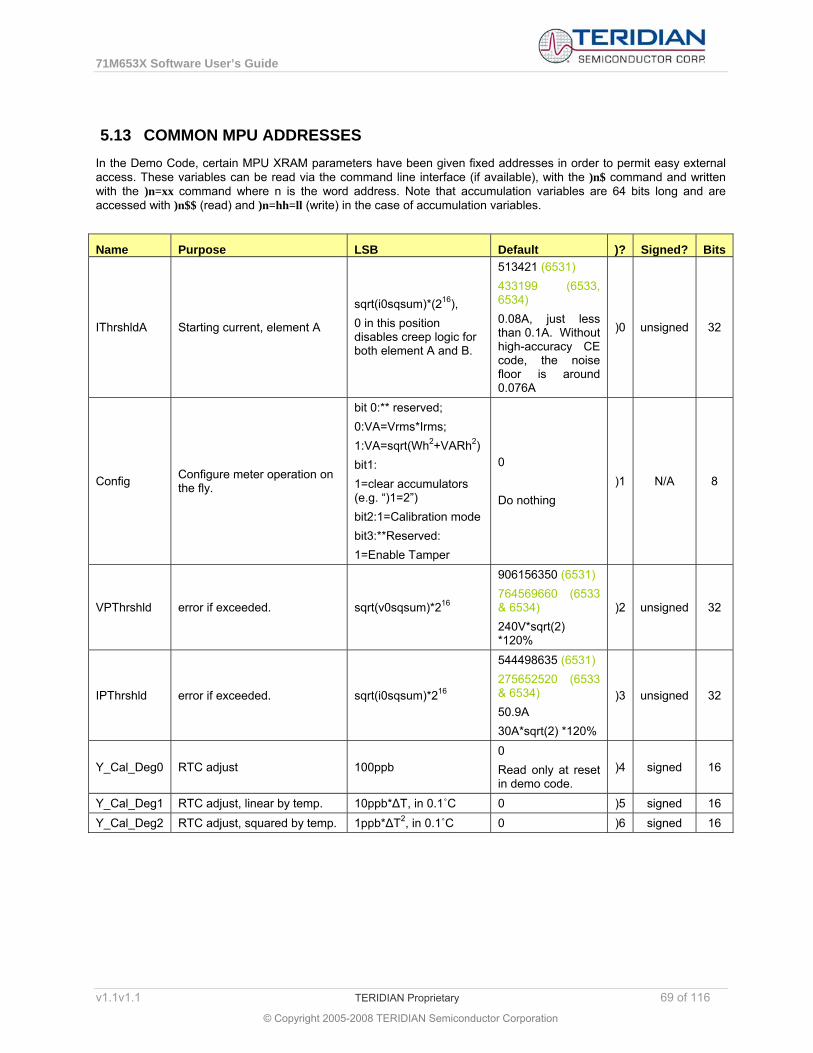
71M653X Software User’s Guide
5.13 COMMON MPU ADDRESSES In the Demo Code, certain MPU XRAM parameters have been given fixed addresses in order to permit easy external access. These variables can be read via the command line interface (if available), with the )n$ command and written with the )n=xx command where n is the word address. Note that accumulation variables are 64 bits long and are accessed with )n$$ (read) and )n=hh=ll (write) in the case of accumulation variables.
Name Purpose LSB Default )? Signed? Bits
IThrshldA Starting current, element A
sqrt(i0sqsum)*(216), 0 in this position disables creep logic for both element A and B.
513421 (6531) 433199 (6533, 6534) 0.08A, just less than 0.1A. Without high-accuracy CE code, the noise floor is around 0.076A
)0 unsigned 32
Config Configure meter operation on the fly.
bit 0:** reserved; 0:VA=Vrms*Irms; 1:VA=sqrt(Wh2+VARh2) bit1: 1=clear accumulators (e.g. “)1=2”) bit2:1=Calibration mode bit3:**Reserved: 1=Enable Tamper
0 Do nothing
)1 N/A 8
VPThrshld sqrt(v0sqsum)*216
906156350 (6531) 764569660 (6533 & 6534) 240V*sqrt(2) *120%
)2 unsigned 32 error if exceeded.
error if exceeded. sqrt(i0sqsum)*216
544498635 (6531) 275652520 (6533 & 6534) 50.9A 30A*sqrt(2) *120%
)3 unsigned IPThrshld 32
Y_Cal_Deg0 RTC adjust 100ppb 0 Read only at reset in demo code.
)4 signed 16
Y_Cal_Deg1 RTC adjust, linear by temp. 10ppb*ΔT, in 0.1˚C 0 )5 signed 16 Y_Cal_Deg2 RTC adjust, squared by temp. 1ppb*ΔT2, in 0.1˚C 0 )6 signed 16
v1.1v1.1 TERIDIAN Proprietary 69 of 116
© Copyright 2005-2008 TERIDIAN Semiconductor Corporation

71M653X Software User’s Guide
PulseWSource PulseVSource
Wh Pulse source, VARh pulse source selection
0=wsum 1=w0sum 2=w1sum 3=w2sum‡ 4=varsum 5=var0sum 6=var1sum 7=var2sum‡ 8=i0sqsum 9=i1sqsum 10=i2sqsum‡ 11=insqsum 12=v0sqsum 13=v1sqsum† 14=v2sqsum‡ 15=vasum** 16=va0sum** 17=va1sum** 18=va2sum‡ 19=wsum_i** 20=w0sum_i** 21=w1sum_i** 22=w2sum_i‡ 23=varsum_i* 24=var0sum_i* 25=var1sum_i* 26=var2sum_i‡ 27=wsum_e** 28=w0sum_e** 29=w1sum_e** 30=w2sum_e‡ 31=varsum_e** 32=var0sum_e** 33=var1sum_e** 34=var2sum_e‡
0 (wsum) 4 (varsum) In demo code, these are the values from the element with the maximum current. A different equation can be chosen as a compilation option, and these become sums.
)7 )8
unsigned 8
v1.1v1.1 TERIDIAN Proprietary 70 of 116
© Copyright 2005-2008 TERIDIAN Semiconductor Corporation

71M653X Software User’s Guide
Vmax Scaling Maximum Volts for PCB 0.1V
6000 600.0V, from the PCB’s design.
)9 unsigned 16
ImaxA Scaling Maximum Volts for PCB element A
0.1A 2080 208.0A, from the PCB’s design.
)A unsigned 16
ppmc1 ADC linear adjust with temperature
parts per million per degree centigrade
0 temp_nom, )14, must be set to a real value from ]7B before this can work. Then it should become -150
)B signed 16
ppmc2 ADC quadratic adjust with temperature
parts per million per degree centigrade squared
0 Should become -392 after setting temp_nom
)C signed 16
Pulse 3 source
Source for software pulse output 3** Indexed as )7
0 wsum; requires software pulse module.
)D unsigned 8
Pulse 4 source
Source for software pulse output 4** Indexed as )7
4 varsum; requires software pulse module.
)E unsigned 8
Scal Accumulation intervals of autocalibration**
Count of accumulation intervals of calibration.
2 2 accumulation intervals covers both chop polarities.
)F unsigned 16
Vcal Volts of autocalibration**
0.1V rms of AC signal applied to all elements during calibration.
2400 240V is a standard full-scale set-up for meter test.
)10 unsigned 16
Ical Amps of autocalibration**
0.1A rms of AC signal applied to all elements during calibration. Power factor must be 1.
300 30A is a standard full-scale set-up for meter test.
)11 unsigned 16
VThrshld
Volts at which to measure frequency, zero crossing, etc.
sqrt(v0sqsum)*216
88992958 (6531) 75087832 (6533 & 6534) 40V A real meter should use sag, but the demo operates with a power supply.
)12 unsigned 16
v1.1v1.1 TERIDIAN Proprietary 71 of 116
© Copyright 2005-2008 TERIDIAN Semiconductor Corporation
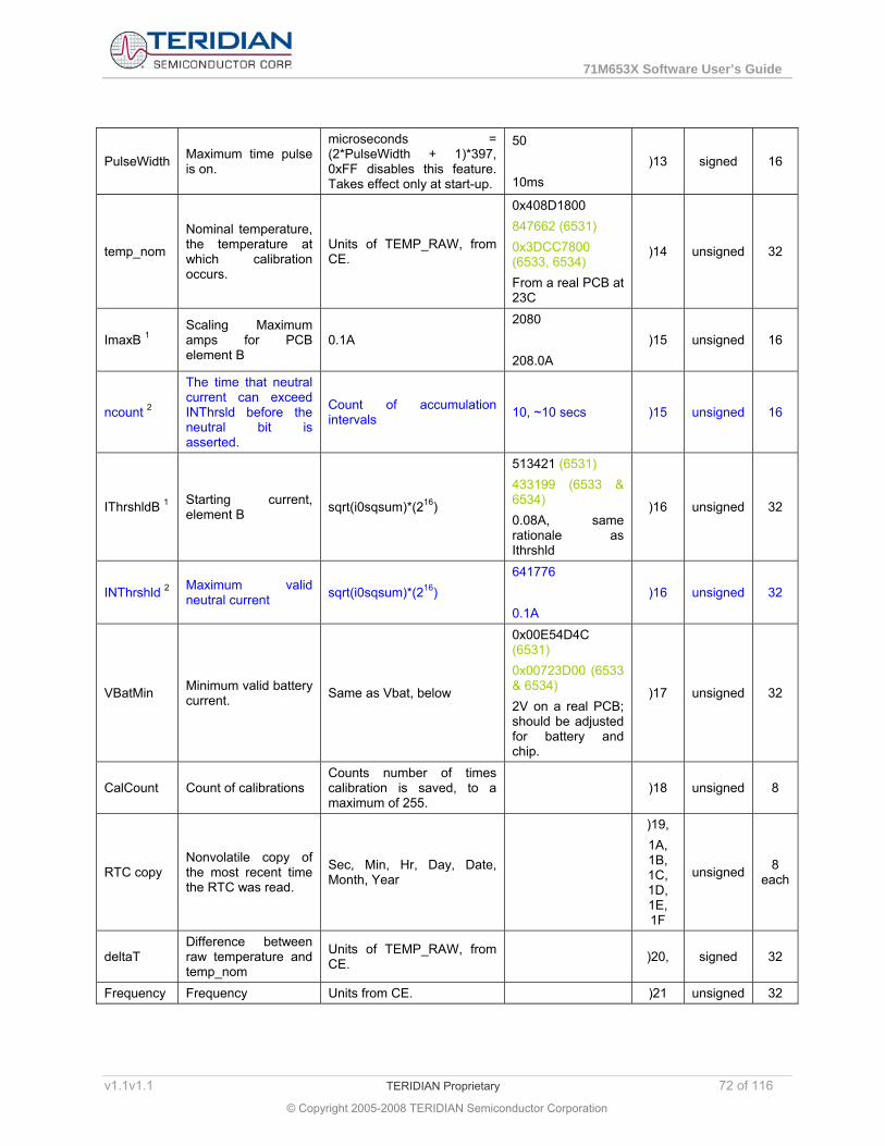
71M653X Software User’s Guide
PulseWidth Maximum time pulse is on.
microseconds = (2*PulseWidth + 1)*397, 0xFF disables this feature. Takes effect only at start-up.
50 10ms
)13 signed 16
temp_nom
Nominal temperature, the temperature at which calibration occurs.
Units of TEMP_RAW, from CE.
0x408D1800 847662 (6531) 0x3DCC7800 (6533, 6534) From a real PCB at 23C
)14 unsigned 32
ImaxB 1 Scaling Maximum amps for PCB element B
0.1A 2080 208.0A
)15 unsigned 16
ncount 2
The time that neutral current can exceed INThrsld before the neutral bit is asserted.
Count of accumulation intervals 10, ~10 secs )15 unsigned 16
Starting current, element B sqrt(i0sqsum)*(216)
513421 (6531) 433199 (6533 & 6534) 0.08A, same rationale as Ithrshld
)16 unsigned 32 IThrshldB 1
Maximum valid neutral current sqrt(i0sqsum)*(216)
641776 0.1A
)16 unsigned INThrshld 2 32
VBatMin Minimum valid battery current. Same as Vbat, below
0x00E54D4C (6531) 0x00723D00 (6533 & 6534) 2V on a real PCB; should be adjusted for battery and chip.
)17 unsigned 32
CalCount Count of calibrations Counts number of times calibration is saved, to a maximum of 255.
)18 unsigned 8
RTC copy Nonvolatile copy of the most recent time the RTC was read.
Sec, Min, Hr, Day, Date, Month, Year
)19, 1A, 1B, 1C, 1D, 1E, 1F
unsigned 8 each
deltaT Difference between raw temperature and temp_nom
Units of TEMP_RAW, from CE. )20, signed 32
Frequency Frequency Units from CE. )21 unsigned 32
v1.1v1.1 TERIDIAN Proprietary 72 of 116
© Copyright 2005-2008 TERIDIAN Semiconductor Corporation

71M653X Software User’s Guide
Vbat Last measured battery voltage.* (Note: battery voltage is measured once per day, except when it is being displayed).
]7 / (2^9) (ADC counts, logically shifted right 9 bits) )22 unsigned 32
Vrms_A Vrms, element A sqrt(v0sqsum)*(216) )24 unsigned 32 Irms_A Irms, element A sqrt(i0sqsum)*(216) )25 unsigned 32 Vrms_B Vrms, element B**,† sqrt(v1sqsum)*(216) )26 unsigned 32 Irms_B Irms, element B sqrt(i1sqsum)*(216) )27 unsigned 32 Vrms_C Vrms, element C‡ sqrt(v2sqsum)*(216) )28 unsigned 32 Irms_C Irms, element C‡ sqrt(i2sqsum)*(216) )29 unsigned 32
Status Status of meter Bits: See table below.
)2A unsigned 32
CAI Count of accumulation intervals since reset, or last clear (“)1=2”) count )2b signed 32
Whi** Imported Wh, all elements. LSB of w0sum )2c signed 64 Whi_A** Imported Wh, element A “ )2e signed 64 Whi_B** Imported Wh, element B “ )30 signed 64 Whi_C**‡ Imported Wh, element C “ )32 signed 64 VARhi* Imported VARh, all elements. LSB of w0sum )34 signed 64 VARhi_A Imported VARh, element A “ )36 signed 64 VARhi_B Imported VARh, element B “ )38 signed 64 VARhi_C*‡ Imported VARh, element C “ )3A signed 64 VAh** Volt-amps, all elements. LSB of w0sum )3C signed 64 VAh_A** Volt-amps, element A “ )3e signed 64 VAh_B** Volt-amps, element B “ )40 signed 64 VAh_C**‡ Volt-amps, element C “ )42 signed 64 Whe** Exported Wh, all elements. LSB of w0sum )44 signed 64 Whe_A** Exported Wh, element A “ )46 signed 64 Whe_B** Exported Wh, element B “ )48 signed 64 Whe_C**‡ Exported Wh, element C “ )4A signed 64 VARhe** Exported VARh, all elements. LSB of w0sum )4C signed 64 VARhe_A** Exported VARh, element A “ )4e signed 64 VARhe_B** Exported VARh, element B “ )50 signed 64 VARhe_C**‡ Exported VARh, element C “ )52 signed 64 Whn Net metered, all elements LSB of w0sum )54 signed 64 Whn_A Net metered Wh, element A, for autocalibration “ )56 signed 64 Whn_B Net metered Wh, element B, for autocalibration “ )58 signed 64 Whn_C‡ Net metered Wh, element C, for autocalibration “ )5A signed 64 VARhn Net metered VARh, sum, all elements LSB of w0sum )5c signed 64
VARhn_A Net metered VARh, element A, for autocalibration “ )5e signed 64
v1.1v1.1 TERIDIAN Proprietary 73 of 116
© Copyright 2005-2008 TERIDIAN Semiconductor Corporation

71M653X Software User’s Guide
VARhn_B Net metered VARh, element B, for autocalibration “ )60 signed 64 VARhn_C*‡ Net metered VARh, element C, for autocalibration “ )62 signed 64 MainEdgeCnt Count of edges Count of zero-crossings. )64 unsigned 32 Wh Default sum of Wh, nonvolatile LSB of w0sum )65 signed 64 Wh_A Wh, element A, nonvolatile “ )67 signed 64 Wh_B Wh, element B, nonvolatile “ )69 signed 64 Wh_C‡ Wh, element C, nonvolatile “ )6B signed 64 StatusNv Nonvolatile status See Status )6D n/a 32
‡ Three phase chips (i.e. 6533, 6534) only. 1 Two phase chips (i.e. 6531), this compilation option is normally on to enable mixing a shunt and CT as current sensors. Uses same space as neutral current threshold. 2 Three phase chips (i.e. 6533. 6534) with neutral current, this compilation option is normally on to enable tests of neutral current. Uses same space as Threshold B.
Table 5-12: MPU Memory Locations
v1.1v1.1 TERIDIAN Proprietary 74 of 116
© Copyright 2005-2008 TERIDIAN Semiconductor Corporation

71M653X Software User’s Guide
Discussion of the bits in Status:
Bit No.
Discussion Name
CREEP 0 Indicates that all elements are in creep mode. The CE’s pulse variables will be “jammed” with a constant value on every accumulation interval to prevent spurious pulses. Note that creep mode therefore halts pulsing even when the CE’s pulse mode is “internal”.
MINVC‡ 1 Element C has a voltage below VThrshld. This forces that element into creep mode.
PB_PRESS 2 A push button press was recorded at the most recent reset or wake from a battery mode. Recorded because the push button flag in the hardware must be cleared in order to reenter a power-saving mode. May be unused in some softwares.
SPURIOUS 3 An unexpected interrupt was detected.
MINVB 4 Element B has a voltage below VThrshld. This forces that element into creep mode.
MAXVA 5 Element A has a voltage above VThrshldP.
MAXVB 6 Element B has a voltage above VThrshldP.
MAXVC‡ 7 Element C has a voltage above VThrshldP.
MINVA 8 Element A has a voltage below VThrshld. This forces that element into creep mode. It also forces the frequency and main edge count to zero.
WD_DETECT 9 The most recent reset was a watchdog reset. This usually indicates a software error.
MAXIN‡ 10 The neutral current is over INThrshld. In a real meter this could indicate faulty distribution or tampering.
MAXIA 11 The current of element A is over IThrshld. In a real meter this could indicate overload.
MAXIB 12 The current of element B is over IThrshld. In a real meter this could indicate overload.
MAXIC‡ 13 The current of element C is over IThrshld. In a real meter this could indicate overload.
MINT 14 The temperature is below the minimum, -40C, established in option_gbl.h, This is not very accurate in the demo code, because the calibration temperature is usually poorly controlled, and the default temp_nom is usually many degrees off. –40C is the minimum recommended operating temperature of the chip.
MAXT 15 The temperature is above the maximum, 85C, established in option_gbl.h, This is not very accurate in the demo code, because the calibration temperature is usually poorly controlled, and the default temp_nom is usually many degrees off. 85C is the maximum recommended operating temperature of the chip.
BATTERY_BAD 16 Just after midnight, the demo code sets this bit if VBat < VBatMin. The read is infrequent to reduce battery loading to very low values. When the battery voltage is being displayed, the read occurs every second, for up to 20 seconds.
CLOCK_TAMPER 17 Clock set to a new value more than two hours from the previous value.
CAL_BAD 18 Set after reset when the read of the calibration data has a bad longitudinal redundancy check or read failure.
CLOCK_UNSET 19 Set when the clock’s current reading is A) More than a year after the previously saved reading, or B) Earlier than the previously saved reading, or C) There is no previously saved reading. In this case, the clock’s time is preserved, but clock software cannot compensate for drift while it was turned off, because it cannot find the interval of the power failure.
POWER_BAD 20 Set after reset when the read of the power register data has a bad longitudinal redundancy check or read failure in both copies. Two copies are used because a power failure can occur while one of the copies is being updated.
GNDNEUTRAL 21 Indicates that a grounded neutral was detected.
TAMPER 22 Tamper was detected †**
v1.1v1.1 TERIDIAN Proprietary 75 of 116
© Copyright 2005-2008 TERIDIAN Semiconductor Corporation

71M653X Software User’s Guide
Bit No.
Discussion Name
SOFTWARE 23 A software defect was detected. error_software() was called. E.g.: In banked code, a subroutine address outside common code is given as a callback routine. Or: irq_enable() (interrupt disable) is called more than irq_disable().
SAGA 25 Element A has a sag. Set in real time by the CE and detected by the ce_busy interrupt (ce_busy_isr() in ce.c) within 8 sample intervals, about 2.6ms. A transition from normal operation to SAGA causes the power registers to be saved, because the demo PCB is powered from element A. For a multiphase power supply, modify the bit mask constant POWERED_PHASE, in options.h to select the sag bits from the most-significant 8 bits of Status, then recompile. In this case, all the bits in POWERED_PHASE must become asserted to cause a save of the powered registers.
SAGB 26 Element A has a sag. Set in real time by the CE and detected by the ce_busy interrupt (ce_busy_isr() in ce.c) within 8 sample intervals, about 2.6ms. On the 6520, the demo code operates with an equation that does not use element B’s voltage, but the meter simulates this by wiring element A’s V to VB on the chip.
SAGC‡ 27 Element C has a sag. Works like other sag bits.
F0_CE 28 A square wave at the line frequency, with a jitter of up to 8 sample intervals, about 2.6ms. The jitter is caused because the ce_busy interrupt only executes all of its code every 8th sample interval.
ONE_SEC 31 Changes each accumulation interval.
‡ Three phase chips (i.e. 6533, 6534) only.
Table 5-13: MPU Status Bits
v1.1v1.1 TERIDIAN Proprietary 76 of 116
© Copyright 2005-2008 TERIDIAN Semiconductor Corporation

71M653X Software User’s Guide
5.14 FIRMWARE APPLICATION INFORMATION
5.14.1 General Design Considerations
5.14.1.1 Multitasking
The meter appears to do many things at once. How does this happen?
Each “task” is a subroutine call in the main loop in Main\main.c: main_run(). The tasks are called repeatedly by the main loop, giving each of them many opportunities to use the MPU. They usually check for “data present”, and then either exit or process the data and then exit. Prominent examples include: meter_run() in meter\meter.c (the meter’s main process), cli() in cli\cli.c (the command line interface’s process), stm_run() in Util\stm.c (the software timers’ update task).
This scheme is well suited to such a small system, but it also has problems when an IO process must wait for input or output. This happens in only two major subsystems, the serial command line interface, and the metering system.
While the serial command logic is waiting for another serial character, it calls a subset of the main loop, in Main\main.c main_background(). main_background() does all of the meter’s main loop except for serial protocols. In that way, the meter keeps “running” while the serial IO is “waiting.”
The main metering routine, Meter\meter.c meter_run(), skips most of its logic until a flag, ce_update, is set. At this point meter_run() runs to completion. meter_run() performs many calculations. These calculations stop the rest of the main loop from running for up to several hundred milliseconds (depends on clock speed). This delay is nearly impossible for a person to see, so it does not affect human I/O at all. The time-critical machine I/O during this period is handled by interrupts that buffer data for the main loop.
5.14.1.2 Synchronization
Interrupts do the work that needs immediate attention, then set a flag or count to start code that runs in the main loop. To keep the main loop simple, the flag, the routine to run in the main loop, and the interrupt code should be defined in the class’s .c file. The main loop should just call the “run” routine continually.
Software timers (Util\stm.c, .h) are started by an interrupt that counts every 10 milliseconds in real time. In the main loop, stm_run() decrements software timer variables and runs the associated callback routine if a timer expires. stm_run() calculates the real interval since its last invocation in order to reduce jitter.
The code also has a shared, calibrated delay loop routine, in IO/delay.c. It’s calibrated in the normal clock modes, and runs at reasonable rates in all clock modes, including brownout mode.
State machines are invoked in the main loop. The main loop will just call a “run” routine with no parameters and no returns. No state variables or other state-machine logic will be defined in the main loop.
5.14.1.3 Bank Switching
The code has to be able to grow to fill the 128KB to 256KB memory space of this chip. So, it is bank-switched.
Keil’s standard bank-switching schemes were all tested for speed, and then the fastest was left installed. See Util\L51_BANK.A51, for the modified Keil assembly file that performs the bank switching.
The selected Keil scheme sets the bank-sfr register FL_BANK directly, from code. Keil’s bank-switching scheme has the linker build a table of global subroutine entry-points in common memory. Calls to global subroutines are actually to an entry in the table, which switches the bank and jumps to the the bank-switching routines. The SUG has more details, including debugging suggestions.
Fast interrupts has to be in the common page, so that their code is always available. Slower interrupts have a trampoline in the common page that performs a bank-switching call to the main interrupt code. This permits entire modules to be placed in different banks, so that the code’s functionally-pure structure doesn’t have to be damaged in order to do bank-switching. The trampolines are in Meter\io653x.c, with other shared interrupt logic.
v1.1v1.1 TERIDIAN Proprietary 77 of 116
© Copyright 2005-2008 TERIDIAN Semiconductor Corporation

71M653X Software User’s Guide
The Keil linker’s dependency command must be used to tell the linker about the caller of every routine called via a function pointer. If this is not done, Keil’s address for the called routine is often in a bank, and the bank is rarely the current bank. So, the caller goes to the called routine’s address, but in the wrong bank. This doesn’t work.
When the linker is told that a called routine is called from a caller, then it places a bank-switching stub for that routine in the common bank, and the call via function pointer works splendidly.
The function pointer issue is a problem for the timer code, and the software timer code. These call an error function when they get function pointer addresses greater than 0x7FFF.
5.14.1.4 Economic Usage of RAM
The IC has only 3K of RAM for use by the MPU. There are two main tricks to fit the data in:
• The main-loop organization lets Keil’s linker use overlays to maximum advantage, multiplying the utility of the small amount of RAM.
• Also, the big pieces of stable data are global, and shared. Most of them are in Totals, a large C structure defined in meter\meter.h. Totals contains all MPU calibration and register items. The CE interface is in CE, a large C structure defined in meter\ce653x.h.
The largest unshared items are the serial buffers, defined in serial0cli.c and serial1cli.c. For most people, removing serial1 has no effect at all on the usability of the debug interface, and it frees the port and RAM for use by an AMR system.
5.14.1.5 Trading Space for Speed
The 8051 has seven types of memory space. If used correctly, they can help code run faster.
The Keil compiler provides memory type names like “data” “xdata” and “pdata” so that the programmer can place particular data items in particular memory spaces. See the manual for more information.
Some memory areas are faster to access, because the code to access the memory is shorter. In decreasing order:
The code keeps a few critical high-speed bit-flags in BDATA, the fastest, rarest memory.
The code keeps a few high-speed counters in DATA, a fast data space. This is intentionally underutilized to make room for customer data.
The code makes very little use of IDATA in order to conserve stack space.
The CE’s output registers are mapped to PDATA. This gives the math fast access to the CE output values.
XDATA is used for most variable data.
CODE is used for code, and a few large tables, like the CE’s code and initialization data.
5.14.1.6 Object-Oriented Design
First, is it worth it? An object-oriented design can use the same control code to run similar electronics or data. This has several advantages. The big one for firmware is that the higher levels of the firmware can quickly change to use other related devices with a minimum of introduced defects.
The trick in a small embedded system is to implement a base class (the “integration interface”) in a way that is efficient and not too hard to understand.
In this design, a base class is an include file of macros (i.e. a “.h” file). Two schemes will be used.
When there are several devices or data structures and switching is not needed, each device will have its own .h file. The macros and function prototypes will provide an interface that is the same for all callers. For example, instead of including ser.h, and calling ser0_getc(), this scheme will have the caller include ser0.h, and then call ser_getc(). By including ser1.h, the same calling code can be instantly ported to serial port 1.
If dynamic calling is needed, the .h file can conceal switching code that tests a bit and selects a daughter-class’s methods. For example Cli\sercli.c conceals an interface that can write to either UART, based on a port parameter.
These schemes are efficient in the 8051, producing code as fast as individual calls for each daughter class.
v1.1v1.1 TERIDIAN Proprietary 78 of 116
© Copyright 2005-2008 TERIDIAN Semiconductor Corporation
71M653X Software User’s Guide
The classic C++ scheme uses a table of subroutine pointers for each class. It performs poorly on the 8051. The 8051 accesses tables of indirect addresses rather slowly.
5.14.1.7 Reconfiguring “Glue Logic”
Compilation switches enable cases. In many cases, code can include a different include (.h) file to customize for a different device. If code is not enabled, it shouldn’t run or be in the code.
For released code, or other point releases, an “unifdef” utility will be used to remove unused conditional code. This makes the code easier to read, but reduces flexibility.
5.14.1.8 DSP Operations
Teridian’s solution for providing a superios electricity metering IC has been to use a simplified 32-bit digital signal processor, the CE, triggered by the ADC multiplexer. Since DSP Code is too hard to develop, prewritten DSP code is provided for the CE. This code is suitable for most metering applications, with optimized performance going right to the chip’s noise floor. It helps that metering is a standard application for most customers.
5.14.1.9 Coping with Various Current Sensors
The MPU code has Imax and Imax2. The calculations automatically convert data from phase B into the same units as phase A, if the “dual Imax” compilation option is set. See meter\meter.c RescalePhaseB().
5.14.1.10 User Interface
The main user interface is an RS-232 command line interface with a help system. This consumes a surprisingly large amount of code because it performs line editing.
There is code that controls an LCD. The meter chip has bits in its I/O area that turn each LCD segment on and off. The segments form segments of numerals, etc. Software arranges to turn the right segments on and off in order to show numbers and annunciators. The code for this looks up a bit mask for each character to decide which pieces of numeral to turn on and off.
In this demo software, pressing the pushbutton changes the display items, or wakes the meter from its low power mode. Most meters have at least one operating switch. The classic is a magnetic reed switch controlled by a magnet outside the meter enclosure. Real meters (but not this demo software) use it to step through a menu system.
5.14.1.11 Operating without User Interface
The EEPROM can be initialized in a programmer with the calibration data. This saves the code and data needed by the meter.
5.14.1.12 Communication with a Computer
This demo code implements both a CLI, and the CP. Code is available for FLAG.
The classic scheme, not provided by this demo code, is to use a serial port communicating via either an infra-red LED and phototdiode, or a low-speed current-loop. The infrared interface is popular in areas where the meter-reader has access to the meter. The current-loop is popular when the meters are inside a building. In this case, a connector is avialable on the outside of the building to read all the meters within it.
5.14.1.13 Support of Automatic Meter Reading
The meter must keep running, but must also present a consistent set of data for the asynchronous meter-reading system. The solution is to make a stable copy at a controlled time in the metering cycle, and then let the AMR system read the stable data.
When the hand-held unit logs on, the serial protocol sets a flag (update_register) asking the meter to copy the registers to stable storage. See Meter\meter.c, the call to Update_register() in meter_run(). When the stable copy is available, the flag register_available is set to true.
If a read request occurs while the copy is going on (i.e. register_available is false), the protocol requests that the message be resent (see Flag\Flag0.c orflag1.c, case “R” of the NoError case of do_cmd()). This negative
v1.1v1.1 TERIDIAN Proprietary 79 of 116
© Copyright 2005-2008 TERIDIAN Semiconductor Corporation

71M653X Software User’s Guide
acknowledge is supposed to occur when the message was garbled, but in this case has the effect of delaying the read command until the copy is complete and a stable copy of the meter data is available for use by the protocol.
When the AMR system logs-off, or the AMR interface times out, the flags are reset to mark the stable copy invalid.
5.14.1.14 Communication between MPU and CE
The communication between CE and MPU has evolved since early versions. The current best practice is to divide the CE’s data into four parts.
1. Configuration data set by the MPU, and read by the CE. This includes gains and other static adjustments.
2. Constant data needed by the CE, and never adjusted by the MPU. The MPU simply sets it. It could be fixed, stored in the CE’s program code, but isn’t.
3. Data read and written by both CE and MPU. These usually begin execution as constant values. This includes pulse input values set by the MPU, which can alternatively be set by the CE’s native code, and the main gain adjustment for making the meter run at different speed in different temperatures.
4. Data written by the CE, and initialized by the MPU to zero. This includes all of the CE’s output values.
Parts 1, 2, and 3 are set to defaults from a table of constants in the MPU’s code area.
Part 1 is saved and restored as part of the EEPROM configuration, as an overlay of the constants.
Part 4 is cleared to zero by the MPU, to permit the table of constants to be as small as possible.
In the 6530, unlike earlier versions, reading and writing the CE is transparent because the CE and MPU share the RAM. No copy is necessary, which saves both MPU time, and RAM. The destination table and CE was moved to start of RAM location zero. The CE’s output data was moved to location 0x0200, so that PDATA can still be used to access it quickly.
5.14.1.15 Timing Control
The chip has two high-speed timers. It also has an electronic clock. Further, there is a timer to wake the chip from its low power modes. The demo code has facilities to demonstrate all of these.
5.14.1.16 6531: Calculation of max(VA*IA, VA*IB) Option, Equation 0
The global flow of Wh calculation is an important optimization, and will be selected by compile flag:
Vrms_A = sqrt(v0sqsum) from the CE.
Irms_A = sqrt(i0sqsum) from the CE.
Irms_B = sqrt(i1sqsum) from the CE.
Volts and Current are now available for all elements.
Figure Wh, VARh and VAh for this accumulation interval:
If Vrms_A < Vthreshold (i.e. there’s no voltage, probably tampering)
Figure watts with a default voltage, but don’t lie about sensed voltage:
Vrms_A = 0
if abs(Irms_A) > IThreshold,
va0sum = Irms_A * defaultV
w0sum = va0sum
else
set them to zero
varh0 = 0
Repeat for element B
else
v1.1v1.1 TERIDIAN Proprietary 80 of 116
© Copyright 2005-2008 TERIDIAN Semiconductor Corporation
71M653X Software User’s Guide
Get Wh (wxsum) and VARh (varxsum) from CE:
w0sum, w1sum (element Wh for one accumulation interval),
var0sum, var1sum (element VARhs are from CE.
va0sum = sqrt(w0sum2 + var0sum2)
va1sum = sqrt(w0sum2 + var0sum2)
endif
va0sum, va1sum, w0sum, w1sum, var0sum, var1sum are now available.
Figure current, the best available way:
If Irms_A < noise-floor of current measurement && Vrms_A > 0
Irms_A = va0sum/Vrms_A
If Irms_N < noise-floor of current measurement && Vrms_A > 0
Irms_B = va1sum/Vrms_A
Do the creep calculation:
If (Vrms_A < Vthreshold)
creep mode, set element A and B’s voltage, current and watts to zero
else
if (Irms_A < Ithreshold)
creep mode: set element A’s current and watts to zero
if (Irms_B < Ithreshold)
creep mode: set element B’s current and watts to zero
Set the pulse outputs.
Sum positive values to normal registers, negative values to export registers.
5.14.1.17 6534: Calculation of VA*IA+VB*IB+VC*IC Option, Equation 5
The global flow of Wh calculation is an important optimization, and will be selected by compile flag:
Vrms_A = sqrt(v0sqsum) from the CE.
Irms_A = sqrt(i0sqsum) from the CE.
etc. for B and C
Volts and Current are now available for all elements.
Figure Wh, VARh and VAh for this accumulation interval:
If Vrms_A < Vthreshold (i.e. there’s no voltage, probably tampering)
Figure watts with a default voltage, but don’t lie about sensed voltage:
Vrms_A = 0
if abs(Irms_A) > IThreshold,
va0sum = Irms_A * defaultV
w0sum = va0sum
else
set them to zero
varh0 = 0
else
v1.1v1.1 TERIDIAN Proprietary 81 of 116
© Copyright 2005-2008 TERIDIAN Semiconductor Corporation

71M653X Software User’s Guide
Get Wh (w0sum) and VARh (var0sum) from CE:
va0sum = sqrt(w0sum2 + var0sum2)
endif
Repeat for elements B and C
va0sum,.. va2sum, w0sum,.. w2sum, var0sum,.. var2sum are now available.
Figure current, the best available way:
If Irms_A < noise-floor of current measurement && Vrms_A > 0
Irms_A = va0sum/Vrms_A
Repeat for elements B and C
Do the creep calculation:
If (Vrms_A < Vthreshold)
creep mode, set element A’s voltage, current and watts to zero
else
if (Irms_A < Ithreshold)
creep mode: set element A’s current and watts to zero
Repeat for element B and C
Set the pulse outputs.
Sum positive values to normal registers, negative values to export registers.
5.14.1.18 How Register Data is Stored
The registers cannot just be kept as a floating point number. When floating point numbers are added, the mantissa of the smaller number has to be shifted to the right, losing precision, so that it can be added to the mantissa of the larger. In less than an hour, a meter implemented with 32-bit floating point arithmetic begins losing billing revenue because of underflow.
In the Teridian implementation, a variable wh_cnt contains the number of CE counts per Wh.
The registers are stored as a 32-bit count of Wh, and a 32-bit remainder in CE counts. The math adds the new CE value to the fractional part, and then transfers even Whs to the Wh count. To do that, it divides the fraction by wh_cnt to get the new Wh to add to the count of Wh. Then, it multiples the number of Wh by wh_cnt to get the number of CE counts to subtract from the fractional CE count. This logic is in normalize8() inUtil\math.c.
This scheme has no underflow. It has a tiny, controlled round-off of ½ of a CE LSB per Wh, which the CE calibration arranges to average to zero. Otherwise, all the fractional data is preserved. The overflow is perfectly controlled, and is made to wrap around to zero at a decimal limit.
The register logic is applied so that the registers only increase. Negative values of watt hours are subtracted from an “export” register.
wh_cnt does not usually change; in a real meter, this would be a constant, not a variable. However, in TSC’s demo meter, the Imax and Vmax (see glossary) are variables, and therefore so must the CE counts per Wh. So, wh_cnt is recalculated on each accumulation interval by the routine wh_cnt_set(), defined in Util\math.c.
Unlike earlier demo code versions, this register math is easy to modify to use realistic units. The WH_RESOLUTION (in Util\mmath.h) is already realistic number, 1.0 (Wh), with a UNITS_RANGE limit of a billion (1x10⁹) Wh.
The display routines (in Meter\wh.c) can divide the registers by 1000 in order to display KWh. This is controlled by a compilation flag, DISPLAY_KWH, which also changes the decimal points and labels for the LCD.
The registers cannot be kept only in RAM. If there is a power failure, they would be lost. The logical scheme is to write them to the EEPROM once each accumulation interval. The problem is that the EEPROM has only 1 million writes, and these would be used up in a few years. So, the revenue registers are kept in a special block of memory, the C structure Totals.Acc. This data is saved only when there is a power failure.
v1.1v1.1 TERIDIAN Proprietary 82 of 116
© Copyright 2005-2008 TERIDIAN Semiconductor Corporation
71M653X Software User’s Guide
5.14.1.19 Managing Power Failures
There is no way to delay power failure to a convenient time, so the meter must always have a valid value for its revenue registers. There are two copies of the register data: Totals.Acc, and Totals.AccB. When Totals.Acc is valid, and its checksum is calculated, it is copied to Totals.AccB. Therefore, in normal operation, one of these is always valid.
Both are saved by the power failure detection logic. When the meter starts up, it checks both, and uses the first one with a valid checksum.
Version 4.6 and later implement a true power failure interrupt from the CE. External interrupt INT0 on the MPU is set up on DIO_9, the same pin as Y_PULSE, one of the spare pulse outputs from the CE (see meter\ce_30.c ce_init()). The CE’s configuration variable CE_STATE has four additional bits, 16:19 which enable and select the elements sensed for power failure. The CE detects power failures as before, but now checks selected status bits in order to cause an MPU interrupt. When all of the elements fail, the CE pulses Y_PULSE, causing an MPU interrupt, which saves the power registers to the EEPROM (see ce_sag_isr () in Meter\ce_30.c).
Before version 4.6, the CE detected power failures by detecting when each mains voltage stayed below a threshold for a configurable number of samples, usually 80 decimal, about two cycles. The MPU discovered this state by reading the CE’s status register. The polling test if the CE’s status registers was done in the CE busy interrupt (\meter\ce.c\ce_busy_isr ()), that occurs once per sample time, about every 396 microseconds. To save the MPU’s time, the sample is compared only once per sample.
5.14.1.20 Pulse Counting
In version 4.6 and later, INT0 is used for the sag interrupt, therefore it cannot be used to count pulses. Therefore, the pulse counting assigns timer 1 (formerly unused) to count the watt-hour pulse. The gate of timer 1 is set to the correct DIO, and timer 1 is set to be a 16 bit counter. (see pcnt_init() in Meter\pcnt_30.c)
The counter is read once per second, in the real-time-clock’s timer interrupt.
The counter is read as two 8-bit values. The lower value could turn over while being read. So, the logic re-reads the lower value if the upper value changes. The exact logic is read-upper, read-lower, read-upper second time. If the second time of the upper counter is different from the first, read the lower again.
After that, each second the number of pulses in that second is the current value of the timer’s register less the previous value. This math automatically handles turn-over of the counter as long as less than 32768 pulses occurred in the last second . For example, say the timer turns over from 0xFFFE to 0x0002. In signed 16 bit math, this is 2 – (-2), or 4.
int1 is still used to count VARh, with one interrupt per pulse.
Before version 4.6, int0 counted watt-hour pulses, and int1 counted var-hour pulses.
5.14.1.21 Battery Modes
The IC has several battery modes. See the section on the battery mode logic for more information, including a state diagram, and special problems.
The demo code displays the main watt-hours when the pushbutton is pressed, as an example of a typical need in a real meter. It does this with full use of the battery modes for minimum power.
5.14.1.22 Real-Time Performance
The main figure of merit is the time to update the registers and display a new result. This is about 50 milliseconds when the MPU runs at 5MHz. This is faster than earlier demo codes (i.e. 200ms on the 6513) because:
1. The data from the CE is not copied.
2. CE data is accessed as PDATA. This permits any register to be used as an indirection pointer.
3. The calculations use fast floating point logic, rather than the custom-written 64-bit multiple-precision math of some earlier versions.
v1.1v1.1 TERIDIAN Proprietary 83 of 116
© Copyright 2005-2008 TERIDIAN Semiconductor Corporation

71M653X Software User’s Guide
v1.1v1.1 TERIDIAN Proprietary 84 of 116
© Copyright 2005-2008 TERIDIAN Semiconductor Corporation
5.14.2 Firmware Application: Selected Tasks
5.14.2.1 Sag Detection
A sag is an undervoltage condition that persists for more than one period. A shorter undervoltage condition is called a dip (see Figure Figure 5-1). The occurrence of sags can announce an impending loss of power. Since accumulated energy values etc. in the meter will have to be saved to non-volatile memory in the case of loss of power, a sag can be used to initiate data saving operations. Some applications may instead save or count the sag event for the purpose of recording power quality data.
dip
sag
Figure 5-1: Sag and Dip Conditions
Sag detection is performed by the CE, based on the CE DRAM registers SAG_THR and SAG_CNT. SAG_THR defines the threshold which the input voltage has to be continuously below, and SAG_CNT defines the number of samples required to trigger the sag bit (see Figure 5-2).
16.67ms
SAG_THR
SAG_CNT
84 samples
16.67ms16.67ms
SAG_THR
SAG_CNT
84 samples
Figure 5-2: Sag Event
When the CE detects a sag that meets the sag conditions specified in SAG_THR and SAG_CNT on one of the input voltage channels, it will reflect this in the corresponding bit (SAG for single-phase, or SAG_A, SAG_B, SAG_C for poly-phase) of the CE STATUS Word. See the CE Interface section in the 653X Data Sheet for details.
The demo code saves the power registers to the EEPROM when a sag is detected. It also has a timer to avoid multiple saves because of grid-switching from a recloser or noisy power when the grid starts up. See the 5.4.2.3 about the CE_BUSY interrupt for more information.
See Application Note AN651X_044 for more information.
5.14.2.2 Temperature Measurement
The temperature output of the on-chip temperature sensor (TEMP_RAW) is provided by the CE in CE DRAM location 0x7B. The relative chip temperature deltaT (MPU location 0x20) is derived by subtracting the raw temperature from the nominal temperature (TEMP_NOM) and multiplying it with a constant factor. Thus, once the raw temperature obtained at a known environmental temperature is stored in TEMP_NOM, deltaT will always reflect the deviation from nominal temperature. The scaling is in tenths of Centigrades, i.e. a reading of 75 means that the measured temperature is 7.5°C higher than the reference temperature.

71M653X Software User’s Guide
5.14.2.3 Temperature Compensation for Measurements
The internal voltage reference of the 653X ICs is calibrated during device manufacture. Trim data is stored in on-chip fuses. The temperature coefficients TC1 and TC2 are given as constants that represent typical component behavior.
The bandgap temperature is provided to the embedded MPU, which then may digitally compensate the power outputs. This permits a system-wide temperature correction over the entire system rather than local to the chip. The incorporated thermal coefficients may include the current sensors, the voltage sensors, and other influences. Since the band gap is chopper stabilized via the CHOP_EN bits, the most significant long-term drift mechanism in the voltage reference is removed.
The CE applies the gain supplied by the MPU in GAIN_ADJ. This external type of compensation enables the MPU to control the CE gain based on any variable, and when EXT_TEMP = 15, GAIN_ADJ is an input to the CE.
5.14.2.4 Temperature Compensation for the RTC
The flexibility provided by the MPU allows for compensation of the RTC using the substrate temperature. To achieve this, the crystal has to be characterized over temperature and the three coefficients Y_CAL, Y_CALC, and Y_CAL_C2 have to be calculated. Provided the IC substrate temperatures tracks the crystal temperature the coefficients can be used in the MPU firmware to trigger occasional corrections of the RTC seconds count, using the RTC_DEC_SEC or RTC_INC_SEC registers in I/O RAM.
Example: Let us assume a crystal characterized by the measurements shown in Table 5-14.
Deviation from
Nominal Temperature [°C]
Measured Frequency [Hz]
Deviation from Nominal
Frequency [PPM] +50 32767.98 -0.61 +25 32768.28 8.545
0 32768.38 11.597 -25 32768.08 2.441 -50 32767.58 -12.817
Table 5-14: Frequency over Temperature
The values show that even at nominal temperature (the temperature at which the chip was calibrated for energy), the deviation from the ideal crystal frequency is 11.6 PPM, resulting in about one second inaccuracy per day, i.e. more than some standards allow. As Figure 5-3 shows, even a constant compensation would not bring much improvement, since the temperature characteristics of the crystal are a mix of constant, linear, and quadratic effects.
32767.532767.632767.732767.832767.9
3276832768.132768.232768.332768.432768.5
-50 -25 0 25 50
Figure 5-3: Crystal Frequency over Temperature
v1.1v1.1 TERIDIAN Proprietary 85 of 116
© Copyright 2005-2008 TERIDIAN Semiconductor Corporation

71M653X Software User’s Guide
One method to correct the temperature characteristics of the crystal is to obtain coefficients from the curve in Figure 31 by curve-fitting the PPM deviations A fairly close curve fit is achieved with the coefficients a = 10.89, b = 0.122, and c = –0.00714 (see Figure 32).
f = fnom * (1 + a/106 + T * b/106 + T2* c/106) When applying the inverted coefficients, a curve (see Figure 5-4) will result that effectively neutralizes the original crystal characteristics. The frequencies were calculated using the fit coefficients as follows:
32767.532767.632767.732767.832767.9
3276832768.132768.232768.332768.432768.5
-50 -25 0 25 50
crystalcurve fitinverse curve
Figure 5-4: Crystal Compensation
The MPU Demo Code supplied with the TERIDIAN Demo Kits has a direct interface for these coefficients and it directly controls the QREG and PREG registers. This interface is implemented by the MPU variables Y_CAL, Y_CALC, and Y_CALC2 (MPU addresses 0x04, 0x05, 0x06). For the Demo Code, the coefficients have to be entered in the form:
10002_
100_
10_)( 2 CALCYTCALCYTCALYppmCORRECTION ⋅+⋅+=
Note that the coefficients are scaled by 10, 100, and 1000 to provide more resolution. For our example case, the coefficients would then become (after rounding):
Y_CAL = 109, Y_CALC = 12, Y_CALC2 = 7
Alternatively, the mains frequency may be used to stabilize or check the function of the RTC. For this purpose, the CE provides a count of the zero crossings detected for the selected line voltage in the MAIN_EDGE_X address. This count is equivalent to twice the line frequency, and can be used to synchronize and/or correct the RTC.
5.14.2.5 Validating the Battery
For applications that utilize the RTC it is very important to validate the battery. A brief loss of battery power when the 653X IC is powered down may result in corrupted RTC data.
The battery monitor function can be used to obtain the battery charge status.
After battery power is lost, the RTC is usually invalid, and the MPU start-up code will then set it to read the year 2001, the month January, and the day 1 (2001/01/01). The time information will be 01:01:01. If the MPU firmware program detects the date 01/01/2001 upon power-up or reset, it is safe to conclude that the RTC is corrupted, most likely due to a missing or low-voltage battery.
v1.1v1.1 TERIDIAN Proprietary 86 of 116
© Copyright 2005-2008 TERIDIAN Semiconductor Corporation
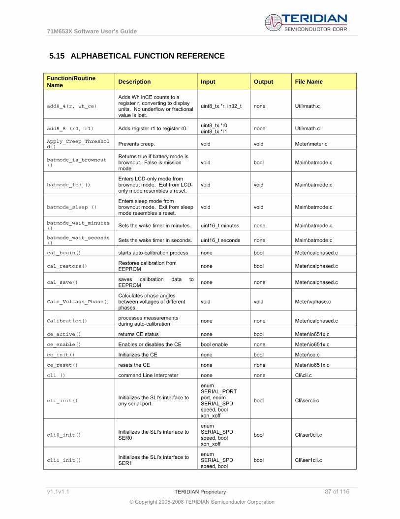
71M653X Software User’s Guide
5.15 ALPHABETICAL FUNCTION REFERENCE Function/Routine Name Description Input Output File Name
add8_4(r, wh_ce)
Adds Wh inCE counts to a register r, converting to display units. No underflow or fractional value is lost.
uint8_tx *r, in32_t none Util\math.c
add8_8 (r0, r1) Adds register r1 to register r0. uint8_tx *r0, uint8_tx *r1 none Util\math.c
Apply_Creep_Threshold() Prevents creep. void void Meter\meter.c
batmode_is_brownout ()
Returns true if battery mode is brownout. False is mission mode
void bool Main\batmode.c
batmode_lcd () Enters LCD-only mode from brownout mode. Exit from LCD-only mode resembles a reset.
void void Main\batmode.c
batmode_sleep () Enters sleep mode from brownout mode. Exit from sleep mode resembles a reset.
void void Main\batmode.c
batmode_wait_minutes () Sets the wake timer in minutes. uint16_t minutes none Main\batmode.c
batmode_wait_seconds () Sets the wake timer in seconds. uint16_t seconds none Main\batmode.c
cal_begin() starts auto-calibration process none bool Meter\calphased.c
cal_restore() Restores calibration from EEPROM none bool Meter\calphased.c
cal_save() saves calibration data to EEPROM none none Meter\calphased.c
Calc_Voltage_Phase() Calculates phase angles between voltages of different phases.
void void Meter\vphase.c
Calibration() processes measurements during auto-calibration none none Meter\calphased.c
ce_active() returns CE status none bool Meter\io651x.c
ce_enable() Enables or disables the CE bool enable none Meter\io651x.c
ce_init() Initializes the CE none bool Meter\ce.c
ce_reset() resets the CE none none Meter\io651x.c
cli () command Line Interpreter none none Cli\cli.c
cli_init() Initializes the SLI's interface to any serial port.
enum SERIAL_PORT port, enum SERIAL_SPD speed, bool xon_xoff
bool Cli\sercli.c
cli0_init() Initializes the SLI's interface to SER0
enum SERIAL_SPD speed, bool xon_xoff
bool Cli\ser0cli.c
cli1_init() Initializes the SLI's interface to SER1
enum SERIAL_SPD speed, bool
bool Cli\ser1cli.c
v1.1v1.1 TERIDIAN Proprietary 87 of 116
© Copyright 2005-2008 TERIDIAN Semiconductor Corporation

71M653X Software User’s Guide
Function/Routine Name Description Input Output File Name
xon_xoff
cmax() returns maximum of unsigned char 'a' and 'b'. uint8_t a, uint8_t b uint8_t Util\math.c
cmd_ce () processes CE commands none none cmd_ce.c
cmd_ce_data_access() Processes context for CE DATA none none Cli\access.c
cmd_download() downloads/uploads code/data between various sources and serial port
none none Cli\load.c
cmd_eeprom() processes EEPROM commands none none Cli\cmd_misc.c
cmd_error() assigns generic command mode error result code none none Cli\cli.c
cmd_load() implements user dialog for data/code download/upload none none Cli\load.c
cmd_meter() processes "M" commands none none Meter\meter.c
cmd_mpu_data_access()
processes context for MPU DATA none none Cli\access.c
cmd_power_save() processes power save command none none Cli\cmd_misc.c
cmd_rtc() processes RTC commands none none Cli\cmd_misc.c
cmd_trim() processes trim commands none none Cli\cmd_misc.c
cmin() returns minimum of unsigned char 'a' and 'b'. uint8_t a, uint8_t b uint8_t Util\math.c
Compute_Phase_Angle() Computes the V/I phase angle. void void Meter\phase_angle.c
Compute_RMS() Computes Vrms and Irms. void void Meter\rms.c
CRC_Calc() calculates standard 16-bit CRC polynomial per ISO/IEC 3309 on flash memory (x16+x12+x5+1)
uint8_tr *ptr, uint16_t len, U01 set
bool Util\flash.c
CRC_Calc_NVR() calculates the 16-bit CRC polynomial per ISO/IEC 3309 on NVRAM
uint8_tx *ptr, uint16_t len, U01 set
bool Util\math.c
ctoh() converts ascii hex character to hexadecimal digit uint8_t c uint8_t Cli\load.c
date_lcd () Displays the current date. void void IO\rtc_30.c
Delta_Time () Figure the elapsed time between two times.
struct RTC_t start, struct RTC_t end
int32_t seconds IO\rtc_30.c
Determine_Frequency()
Sets the frequency. Uses sag status and voltage thresholds to return 0 if the voltages are off.
void void Meter\freq.c
Determine_Peaks()
Sets status bits if voltages, currents or temperature are outside limits. Sag tests are in xfer_busy_int()
void void Meter\peak_alerts.c
divide() *u /= *v uint8_tx *u, uint8_tx *v, m, n, uint8_tx *v0
uint8_t Util\math.c
divide_ () *u /= *v uint8_tx *u, uint8_tx *v, m, n, uint8_tx *v0
none Util\math.c
divide_1() *x /= y uint8_tx *x, y, n none Util\math.c
v1.1v1.1 TERIDIAN Proprietary 88 of 116
© Copyright 2005-2008 TERIDIAN Semiconductor Corporation

71M653X Software User’s Guide
Function/Routine Name Description Input Output File Name
done() exits control uint8_td *c *c Cli\cli.c
EEProm_Config() connects/disconnects DIO4/5 for I2C interface to serial EEPROM
bool access, uint16_t page_size, uint8_t tWr
none IO\eeprom.c, IO\eepromp3.c
es0_isr () serial port 0 service routine none none IO\ser0.c
es1_isr() serial port 1 service routine none none IO\ser1.c
frequency_lcd () Displays the frequency on the LCD. void void Meter\freq.c
get_ce_constants()
Copies CE configuration constants to a data structure so they can be viewed in the emulator.
void void Meter\ce.c
get_char() gets next character from CLI buffer none uint8_t cli\io.c
get_char_d() gets next character from CLI buffer uint8_t idata *d uint8_t cli\io.c
get_digit() gets next decimal (or hex) digit from CLI buffer uint8_t idata *d uint8_t cli\io.c
get_long() converts ascii decimal (or hex) long to binary number none int32_t cli\io.c
get_long_decimal() converts ascii decimal long to binary number. uint8_t c int32_t cli\io.c
get_long_hex() converts ASCII hexadecimal number to binary number none U32 cli\io.c
get_num() converts ascii decimal (or hex) number to binary number none S08 cli\io.c
get_num_decimal() converts ascii decimal number to binary number none S08 cli\io.c
get_num_hex() converts ascii hexdecimal byte to binary number none uint8_t cli\io.c
get_short() converts ascii decimal (or hex) short to binary number none int16_t cli\io.c
get_short_decimal() converts ascii decimal short to binary number none int16_t cli\io.c
get_short_hex() converts ascii hexdecimal short to binary number none uint16_t cli\io.c
htoc() converts hexadecimal digit to ascii hex character uint8_t c uint8_t Cli\load.c
IICGetBit() gets a bit, used to reset some parts none uint8_t io\iiceep.c
IICInit() initializes DIO4/5 as EEPROM interface none none io\iiceep.c
IICStart() IIC bus's start condition none none io\iiceep.c
IICStop() IIC bus's stop condition none none io\iiceep.c
init_meter() Initializes meter to default values none none defaults.c
IRQ_DEFINES Defines variables used by macros to enable and disable interrupts.
n/a n/a util\irq.h
v1.1v1.1 TERIDIAN Proprietary 89 of 116
© Copyright 2005-2008 TERIDIAN Semiconductor Corporation

71M653X Software User’s Guide
Function/Routine Name Description Input Output File Name
irq_disable() Disables interrupts. void void util\irq.c
IRQ_DISABLE()
The fastest way to disable interrupts. Requires IRQ_DEFINES to be earlier in the code, or that the needed symbols be defined.
n/a n/a util\irq.h
irq_enable() Enables interrupts void void util\irq.c
IRQ_ENABLE()
The fastest way to enable interrupts. Requires IRQ_DEFINES to be earlier in the code, or that the needed symbols be defined.
n/a n/a util\irq.h
irq_init() Initializes interrupt control. void void util\irq.c
labsx() returns the absolute value int32_t x S332 Util\math.c
latan2() returns the arcTangent int32_t sy, int32_t sx U32 Util\math.c
LCD_CE_Off() displays “CE OFF” on LCD none none io\lcd.c
LCD_Command() turns LCD on or off, clears display uint8_t LcdCmd none io\lcd.c
LCD_Config() configures LCD parameters
uint8_t num, enum eLCD_mode bias, enum LCD_CLK clock
none io\lcd.c
LCD_Data_Read() reads from selected icon of LCD uint8_t Icon uint16_t io\lcd.c
LCD_Data_Write() writes to selected icon of LCD uint8_t icon, uint16_t Mask none io\lcd.c
LCD_Hello() displays “HELLO” on LCD none none io\lcd.c
LCD_Init() clears LCD, enables LCD segment drivers none none io\lcd.c
LCD_Mode Display a mode number. Uint8_t mode none io\lcd.c
LCD_Number() Displays a number on the LCD.
Int32_t number uint8_t num_digits_before_decimal_point, uint8_t num_digits_after_decimal_point
none io\lcd.c
lmax() returns maximum of unsigned long ‘a’ and ‘b’. U32 a, U32 b U32 Util\math.c
lmin() returns minimum of unsigned long ‘a’ and ‘b’. U32 a, U32 b U32 Util\math.c
log2() returns binary logarithm uint16_t k uint8_t Util\math.c
LRC_Calc_NVR () Calculates a longitudinal redundancy check (bitwise parity)
Bool (ok/bad) Pointer, length, set Util\library.c
Lroundf() Returns long rounded from float. Standard C99 library routine not provided by Keil
Long Float Util\math.c
main_background() executes background processing none none main.c
main_edge_cnt_lcd () Displays either the Uint8_t select void Meter\freq.c
v1.1v1.1 TERIDIAN Proprietary 90 of 116
© Copyright 2005-2008 TERIDIAN Semiconductor Corporation
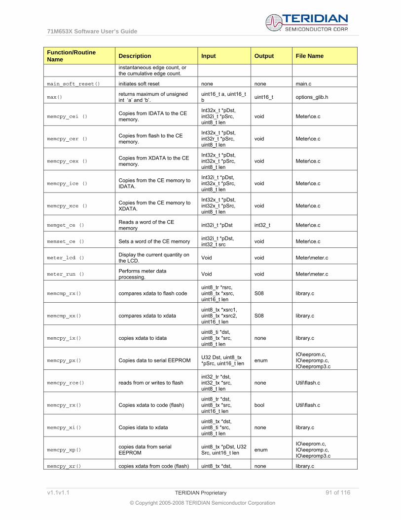
71M653X Software User’s Guide
Input Output File Name Function/Routine Name Description
instantaneous edge count, or the cumulative edge count.
initiates soft reset main_soft_reset() none none main.c
max() returns maximum of unsigned int ‘a’ and ‘b’.
uint16_t a, uint16_t b uint16_t options_glib.h
memcpy_cei () Copies from IDATA to the CE memory.
Int32x_t *pDst, int32i_t *pSrc, uint8_t len
void Meter\ce.c
memcpy_cer () Copies from flash to the CE memory.
Int32x_t *pDst, int32r_t *pSrc, uint8_t len
void Meter\ce.c
memcpy_cex () Copies from XDATA to the CE memory.
Int32x_t *pDst, int32x_t *pSrc, uint8_t len
void Meter\ce.c
memcpy_ice () Copies from the CE memory to IDATA.
Int32i_t *pDst, int32x_t *pSrc, uint8_t len
void Meter\ce.c
memcpy_xce () Copies from the CE memory to XDATA.
Int32x_t *pDst, int32x_t *pSrc, uint8_t len
void Meter\ce.c
memget_ce () Reads a word of the CE memory int32i_t *pDst int32_t Meter\ce.c
memset_ce () Sets a word of the CE memory int32i_t *pDst, int32_t src void Meter\ce.c
meter_lcd () Display the current quantity on the LCD. Void void Meter\meter.c
meter_run () Performs meter data processing. Void void Meter\meter.c
memcmp_rx() compares xdata to flash code uint8_tr *rsrc, uint8_tx *xsrc, uint16_t len
S08 library.c
memcmp_xx() compares xdata to xdata uint8_tx *xsrc1, uint8_tx *xsrc2, uint16_t len
S08 library.c
memcpy_ix() copies xdata to idata uint8_ti *dst, uint8_tx *src, uint8_t len
none library.c
memcpy_px() Copies data to serial EEPROM U32 Dst, uint8_tx *pSrc, uint16_t len enum
IO\eeprom.c, IO\eepromp.c, IO\eepromp3.c
memcpy_rce() reads from or writes to flash int32_tr *dst, int32_tx *src, uint8_t len
none Util\flash.c
memcpy_rx() Copies xdata to code (flash) uint8_tr *dst, uint8_tx *src, uint16_t len
bool Util\flash.c
memcpy_xi() Copies idata to xdata uint8_tx *dst, uint8_ti *src, uint8_t len
none library.c
memcpy_xp() copies data from serial EEPROM
uint8_tx *pDst, U32 Src, uint16_t len enum
IO\eeprom.c, IO\eepromp.c, IO\eepromp3.c
memcpy_xr() copies xdata from code (flash) uint8_tx *dst, none library.c
v1.1v1.1 TERIDIAN Proprietary 91 of 116
© Copyright 2005-2008 TERIDIAN Semiconductor Corporation

71M653X Software User’s Guide
Function/Routine Name Description Input Output File Name
uint8_tr *src, uint16_t len
memcpy_xx() copies xdata to xdata uint8_tx *dst, uint8_tx *src, uint16_t len
none library.c
memset_x() sets xdata to specified value uint8_tx *dst, uint8_t s, uint16_t len
none library.c
meter_initialize() initializes most I/O functions thaty read line power none none meter.c
meter_totals () Display a selected quantity on the LCD.
Uint8_t select,uint8_t phase
void meter.c
microseconds2tmr_reg() Converts to timer’s count. Number uint16_t tmr0.h, tmr1.h
milliseconds() Converts milliseconds to clock ticks, usually for a software timer.
Any number uint16_t stm.h
milliseconds2tmr_reg() Converts to timer’s count. Number uint16_t tmr0.h, tmr1.h
min() returns minimum of unsigned int ‘a’ and ‘b’.
uint16_t a, uint16_t b uint16_t options_glib.h
MPU_Clk_Select() selects MPU clock speed enum MPU_SPD speed bool IO\serial.c
MPU_Clk_Select() Describes the clock speed of the MPU to a serial interface.
Enum SERIAL_PORT port, enum eMPU_DIV speed
bool Cli\sercli.c
MPU_Clk_Select0() Describes the clock speed of the MPU to the serial interface.
Enum eMPU_DIV speed bool Cli\ser0cli.c
MPU_Clk_Select1() Describes the clock speed of the MPU to the serial interface.
Enum eMPU_DIV speed bool Cli\ser1cli.c
multiply_1() W = x * y uint8_tx *w, uint8_tx *x, y, n uint8_t Util\math.c
multiply_4_1() (uint32_t) w = (uint32_t) x * (uint8_t) y
uint8_tx *w, uint8_tx *x, y uint8_t Util\math.c
multiply_4_4() (uint64_t) w = (uint32_t) x * (uint32_t) y
uint8_tx *w, uint8_tx *x, uint8_tx *y
none Util\math.c
multiply_8_1() (uint64_t) w = (uint64_t) x * (uint8_t) y
uint8_tx *w, uint8_tx *x, y uint8_t Util\math.c
multiply_8_4() (uint96_t) w = (uint64_t) x * (uint32_t) y
uint8_tx *w, uint8_tx *x, uint8_tx *y
none Util\math.c
normalize8()
Puts a register into normal form. I.e., fractional part is less than one display unit, both units and fraction are positive or zero, and display units is less than the UNITS_RANGE.
Uint8_tx *r void Util\math.c
operating_lcd () Displays the number of hours of operation. Void void Io\rtc_30.c
OperatingHours() Calculates hours of operation from the last valid mark. None int32_t hours Io\rtc_30.c
v1.1v1.1 TERIDIAN Proprietary 92 of 116
© Copyright 2005-2008 TERIDIAN Semiconductor Corporation

71M653X Software User’s Guide
Function/Routine Name Description Input Output File Name
OSCOPE_INIT Defines DIO_7, the VAR pulse output as a DIO. N/a n/a Util\oscope.h
OSCOPE_ONE Set DIO_7, the same pin as the VARh pulse output, to high. N/a n/a Util\oscope.h
OSCOPE_TOGGLE Inverts DIO_7, the same pin as the VARh pulse output. N/a n/a Util\oscope.h
OSCOPE_ZERO Set DIO_7, the same pin as the VARh pulse output, to low. N/a n/a Util\oscope.h
pcnt_accumulate() Accumulates counts from the previous second. Void void Meter\pcnt.c
pcnt_init () Initialize logic to count output pulses. Void void Meter\pcnt.c
pcnt_lcd() Display pulse count on LCD uint8_t select void Meter\pcnt.c
pcnt_start() Starts plse-counting for a fixed number of seconds. Int16_t seconds void Meter\pcnt.c
pcnt_update() Synchronizes pulse counts with noninterrupting code. Void void Meter\pcnt.c
phase_angle_lcd () Displays a V/I phase angle. Uint8_t phase void meter\phase_angle.c
psoft_init () Initializes software pulse outputs. Void void Meter\psoft.c
psoft_out() Generates two additional pulse outputs. Call from ce_busy_isr void void Meter\psoft.c
psoft_update ()
The inputs are watt hours, as generated by the CE, and set the extra pulse generators to blink at the same rate as CE pulse outputs, with the same units. This should be called each time a new accumulation interval has data.
int32_t pulse3_in, int32_t pulse4_in void Meter\psoft.c
put_char() puts character into CLI buffer uint8_t idata *c none cli\io.c
Read_Trim() reads the trim value for selected trim word enum eTRIM select S08 Meter\io653x.c
rms_I_lcd() Displays current. Uint8_t phase void Meter\rms.c
rms_v_lcd() Displays voltage. Uint8_t phase void Meter\rms.c
RTC_Adjust_Trim() Safely sets the compensation variables.
Bool clr_cnt, int32_t value none IO\rtc_30.c
RTC_Compensation() Calculates and adjusts the temperature compensation for the RTC.
None none IO\rtc_30.c
rtc_isr () Interrupt code to adjust clock each second. Void void IO\rtc_30.c
RTClk_Read() reads current values of RTC none none IO\rtc_30.c
RTClk_Reset() resets the RTC none none IO\rtc_30.c
RTC_Trim() Calculates the temperature compensation using Y_Cals none int32_t ppb IO\rtc_30.c
RTClk_Write() writes/sets to RTC none none IO\rtc_30.c
s2f() Returns the floating point CE units value closest to the register value. Can lose up to
uint8x_t *register float util\math.c
v1.1v1.1 TERIDIAN Proprietary 93 of 116
© Copyright 2005-2008 TERIDIAN Semiconductor Corporation
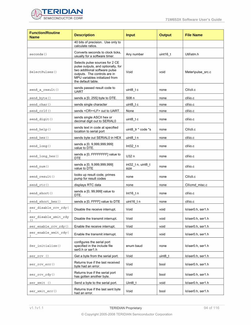
71M653X Software User’s Guide
Input Output File Name Function/Routine Name Description
40 bits of precision. Use only to calculate ratios.
Converts seconds to clock ticks, usually for a software timer. seconds() Any number uint16_t Util\stm.h
SelectPulses()
Selects pulse sources for 2 CE pulse outputs, and optionally, for two additional software pulse outputs. The controls are in MPU variables initialized from the default table.
Void void Meter\pulse_src.c
send_a_result() sends passed result code to UART uint8_t c none Cli\cli.c
send_byte() sends a [0, 255] byte to DTE. S08 n none cli\io.c
send_char() sends single character uint8_t c none cli\io.c
send_crlf() sends <CR><LF> out to UART. None none cli\io.c
send_digit() sends single ASCII hex or decimal digit out to SERIAL0 uint8_t c none cli\io.c
send_help() sends text in code at specified location to serial port uint8_tr * code *s none Cli\cli.c
send_hex() sends byte out SERIAL0 in HEX uint8_t n none cli\io.c
send_long() sends a [0, 9,999,999,999] value to DTE. Int32_t n none cli\io.c
send_long_hex() sends a [0, FFFFFFFF] value to DTE U32 n none cli\io.c
send_num() sends a [0, 9,999,999,999] value to DTE
int32_t n, uint8_t size none cli\io.c
send_result() looks up result code, primes pump for result codes none none Cli\cli.c
send_rtc() displays RTC data none none Cli\cmd_misc.c
send_short() sends a [0, 99,999] value to DTE. Int16_t n none cli\io.c
send_short_hex() sends a [0, FFFF] value to DTE uint16_t n none cli\io.c
ser_disable_rcv_rdy() Disable the receive interrupt. Void void Io\ser0.h, ser1.h
ser_disable_xmit_rdy() Disable the transmit interrupt. Void void Io\ser0.h, ser1.h
ser_enable_rcv_rdy() Enable the receive interrupt. Void void Io\ser0.h, ser1.h
ser_enable_xmit_rdy() Enable the transmit interrupt. Void void Io\ser0.h, ser1.h
Ser_initialize() configures the serial port specified in the include file ser0.h or ser1.h
enum baud none Io\ser0.h, ser1.h
ser_rcv () Get a byte from the serial port. Void uint8_t Io\ser0.h, ser1.h
ser_rcv_err() Returns true if the last received byte had an error. Void bool Io\ser0.h, ser1.h
ser_rcv_rdy() Returns true if the serial port has gotten another byte. Void bool Io\ser0.h, ser1.h
ser_xmit () Send a byte to the serial port. Uint8_t void Io\ser0.h, ser1.h
ser_xmit_err() Returns true if the last sent byte had an error. Void bool Io\ser0.h, ser1.h
v1.1v1.1 TERIDIAN Proprietary 94 of 116
© Copyright 2005-2008 TERIDIAN Semiconductor Corporation

71M653X Software User’s Guide
Function/Routine Name Description Input Output File Name
ser_xmit_free () Unimplemented routine to permit other uses of transmit electronics.
Void void Io\ser0.h, ser1.h
ser_xmit_off () Unimplemented routine to disable transmit electronics. Void void Io\ser0.h, ser1.h
ser_xmit_on () Unimplemented routine to enable transmit electronics. Void void Io\ser0.h, ser1.h
ser_xmit_rdy() Returns true if the serial port can send another byte. Void bool Io\ser0.h, ser1.h
Serial_CRx() Receive a string up to a maximum length.
Enum SERIAL_PORT port, uint8x_t *buffer, uint16_t len
uint16_t length-received
Cli\sercli.c
Serial_CTx() Transmit a string up to a maximum length.
Enum SERIAL_PORT port, uint8x_t *buffer, uint16_t len
uint16_t length-sent Cli\sercli.c
Serial_CRx() gets additional bytes from the receive buffer
enum SERIAL_PORT port, uint8_tx *buffer, uint16_t len
uint16_t Io\sercli.c
Serial_CTx () puts additional bytes into the transmit buffer
enum SERIAL_PORT port, uint8_tx *buffer, uint16_t len
uint16_t Io\sercli.c
Serial_Rx() Receive a string of any length.
Enum SERIAL_PORT port, uint8x_t *buffer, uint16_t len
none Cli\sercli.c
Serial_Rx () sets up receive buffer and starts receiving
enum SERIAL_PORT port, uint8_tx *buffer, uint16_t len
enum SERIAL_RC data
Io\sercli.c
Serial_RxFlowOff() Force an XOFF to be sent on the selected port.
Enum SERIAL_PORT port
none Cli\sercli.c
Serial_RxFlowOn() Force an XON to be sent on the selected port.
Enum SERIAL_PORT port
none Cli\sercli.c
Serial_RxLen() returns the number of bytes received
enum SERIAL_PORT port
uint16_t Io\sercli.c
Serial_Tx() Transmit a string of any length.
Enum SERIAL_PORT port, uint8x_t *buffer, uint16_t len
none Io\sercli.c
Serial_Tx() sets up transmission buffer and starts transmission
enum SERIAL_PORT port, uint8_tx *buffer, uint16_t len
enum SERIAL_RC data
Io\sercli.c
Serial_TxLen() returns the number of bytes left to transmit
enum SERIAL_PORT port
uint16_t Io\sercli.c
Serial0_CRx() Receive a string up to a maximum length.
Uint8x_t *buffer, uint16_t len
uint16_t length- Cli\ser0cli.c
v1.1v1.1 TERIDIAN Proprietary 95 of 116
© Copyright 2005-2008 TERIDIAN Semiconductor Corporation
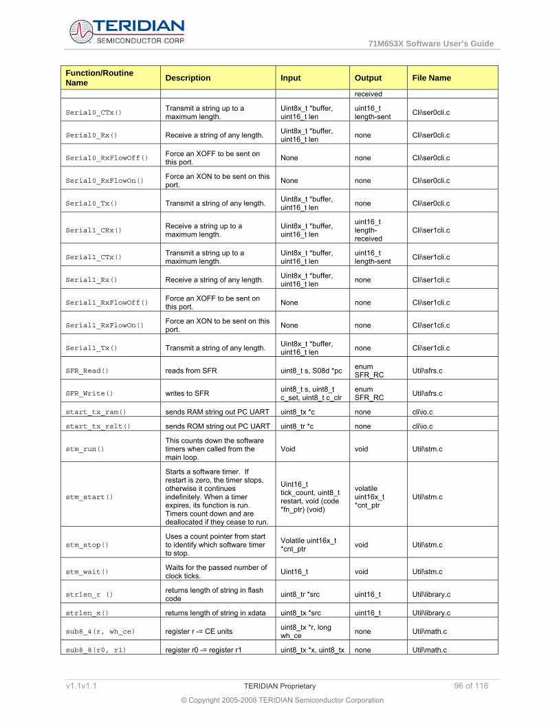
71M653X Software User’s Guide
Function/Routine Name Description Input Output File Name
received
Serial0_CTx() Transmit a string up to a maximum length.
Uint8x_t *buffer, uint16_t len
uint16_t length-sent Cli\ser0cli.c
Serial0_Rx() Receive a string of any length. Uint8x_t *buffer, uint16_t len none Cli\ser0cli.c
Serial0_RxFlowOff() Force an XOFF to be sent on this port. None none Cli\ser0cli.c
Serial0_RxFlowOn() Force an XON to be sent on this port. None none Cli\ser0cli.c
Serial0_Tx() Transmit a string of any length. Uint8x_t *buffer, uint16_t len none Cli\ser0cli.c
Serial1_CRx() Receive a string up to a maximum length.
Uint8x_t *buffer, uint16_t len
uint16_t length-received
Cli\ser1cli.c
Serial1_CTx() Transmit a string up to a maximum length.
Uint8x_t *buffer, uint16_t len
uint16_t length-sent Cli\ser1cli.c
Serial1_Rx() Receive a string of any length. Uint8x_t *buffer, uint16_t len none Cli\ser1cli.c
Serial1_RxFlowOff() Force an XOFF to be sent on this port. None none Cli\ser1cli.c
Serial1_RxFlowOn() Force an XON to be sent on this port. None none Cli\ser1cli.c
Serial1_Tx() Transmit a string of any length. Uint8x_t *buffer, uint16_t len none Cli\ser1cli.c
SFR_Read() reads from SFR uint8_t s, S08d *pc enum SFR_RC Util\sfrs.c
SFR_Write() writes to SFR uint8_t s, uint8_t c_set, uint8_t c_clr
enum SFR_RC Util\sfrs.c
start_tx_ram() sends RAM string out PC UART uint8_tx *c none cli\io.c
start_tx_rslt() sends ROM string out PC UART uint8_tr *c none cli\io.c
stm_run() This counts down the software timers when called from the main loop.
Void void Util\stm.c
stm_start()
Starts a software timer. If restart is zero, the timer stops, otherwise it continues indefinitely. When a timer expires, its function is run. Timers count down and are deallocated if they cease to run.
Uint16_t tick_count, uint8_t restart, void (code *fn_ptr) (void)
volatile uint16x_t *cnt_ptr
Util\stm.c
stm_stop() Uses a count pointer from start to identify which software timer to stop.
Volatile uint16x_t *cnt_ptr void Util\stm.c
stm_wait() Waits for the passed number of clock ticks. Uint16_t void Util\stm.c
strlen_r () returns length of string in flash code uint8_tr *src uint16_t Util\library.c
strlen_x() returns length of string in xdata uint8_tx *src uint16_t Util\library.c
sub8_4(r, wh_ce) register r -= CE units uint8_tx *r, long wh_ce none Util\math.c
sub8_8(r0, r1) register r0 -= register r1 uint8_tx *x, uint8_tx none Util\math.c
v1.1v1.1 TERIDIAN Proprietary 96 of 116
© Copyright 2005-2008 TERIDIAN Semiconductor Corporation

71M653X Software User’s Guide
Function/Routine Name Description Input Output File Name
*y
temperature_lcd() Displays the current delta from the calibration temperature in degrees C on the LCD.
Void void Meter\meter.c
time_lcd () Displays the current time. Void void io\rtc_30.c
tmr_disable () Halt a timer. None none io\tmr0.h, tmr1.h
tmr_enable () Lets a timer run (timer start does this by default) none none io\tmr0.h, tmr1.h
tmr_running () Returns true if the timer is running. none bool io\tmr0.h, tmr1.h
tmr_start () Starts a hardware timer.
Uint16_t time (in timer units), uint8_t restart_flag (zero means interrupt once), void (code *pfn) (void) (code to execute)
none io\tmr0.h, tmr1.h, tmr0.c, tmr1.c
tmr_stop () Stops a hardware timer. None none io\tmr0.h, tmr1.h
tmr0_isr () Timer interrupt for TMR0 none none io\tmr0.c
tmr1_isr () Timer interrupt for TMR1 none none io\tmr1.c
update_register () Move data from AMR’s copy of power registers into power registers.
Void void Meter\meter.c
uwr_busy_wait () Wait for programming complete indication. None none io\uwrdio.c, uwreep.c2
uwr_init () Initialize a 3-wire (similar to uWire™) interface none none io\uwrdio.c, uwreep.c2
uwr_read () Get a counted string of bytes. Uint8x_t *pbOut, uint16_t cnt none io\uwrdio.c, uwreep.c2
uwr_select () Select a chip by passing its address; 0 = none; This must be ported to new PCBs.
Uint8_t address none io\uwrdio.c, uwreep.c2
uwr_write () Transmit a counted string of bytes.
Uint8x_t *pbOut, uint16_t cnt
bool true = success. Io\uwrdio.c, uwreep.c2
Ah_Accumulate() Calculates VAh void void meter\vah.c
VARh_Accumulate() Calculates VARh void void meter\varh.c
voltage_phase_lcd() Display voltage phases on LCD. Uint8_t select void meter\vphase.c
wd_create() Creates a software watchdog. Uint8_t wd void util\wd.c
wd_destroy() Destroys a software watchdog. Uint8_t wd void util\wd.c
wd_reset()
Resets a software watchdog. If all software watchdogs have been reset, the hardware watchdog is reset.
Uint8_t wd void util\wd.c
wh_accumulate() Calculate watt hours. Void void meter\wh.c
wh_brownout_to_lcd() Displays a precalculated 6-digit number. Uint32_t number void meter\wh.c
wh_cnt_set() Sets wh_cnt to the number of CE Wh units per display unit. void void util\math/c
wh_lcd() Displays a watt-hour value on the LCD in milliwatt-hours. uint8_t *val void meter\wh.c
v1.1v1.1 TERIDIAN Proprietary 97 of 116
© Copyright 2005-2008 TERIDIAN Semiconductor Corporation

71M653X Software User’s Guide
Function/Routine Name Description Input Output File Name
wh_sum_export () Adds (0 - w1) to s, only if w1 is negative, yielding a total of exported power in w.
uint8x_t *s, int32i_t *wl void meter\wh.c
Adds w1 to s, only if w1 is positive, yielding a total of imported power in w.
wh_sum_import () uint8x_t *s, int32i_t *wl void meter\wh.c
wh_sum_net() Adds w1 to s, yielding a net sum of watthours in s.
uint8x_t *s, int32i_t *wl void meter\wh.c
wh_to_long ()
Convert a 64-bit internal watts count to a 6-digit value (i.e. this is the routine that precalculates values for wh_brownout_to_lcd()).
uint8_t *val uint32_t meter\wh.c
5.16 ERRATA The up-to-date list of known issues with revision 4.4.15 of the Demo Code can be found in the readme.txt file contained in the 653x_demo ZIP file shipped with the Demo Kits.
The factory should be contacted for updates to the Demo Code.
Known Firmware Errata for version 4.4.15 are listed in the table below. Number Issue Comment
v1.1v1.1 TERIDIAN Proprietary 98 of 116
© Copyright 2005-2008 TERIDIAN Semiconductor Corporation
71M653X Software User’s Guide
5.17 PORTING 71M6511/6513 CODE TO THE 71M653X
5.17.1 Flash Use
The biggest issue when moving code from the 6511/6513 to the 71M653x is the increased program memory. While the 71M6511 and 6513 have 64K, the 71M6531 has 128K and the 71M6534 has 256K. The 653x defaults to a 64K configuration, so code from earlier meter chips will fit easily.
Creating banked code that uses the extra flash is a substantial discussion in itself. See the section “Creating banked code.”
5.17.2 Extra RAM
The MPU now has access to 4K of RAM, up from 2K. Roughly 1K is allocated to the CE, leaving 3K.
5.17.3 CE Data Location is at XDATA 0x0000
CE data now resides in roughly the first 1K bytes of RAM, from 0x0000 to 0x03FF. The exact CE RAM usage varies with different CE code versions, with single-phased CE codes taking less RAM, and three-phase CE codes taking up to the limit. Nonstandard CE codes may take more than 1K, but these will come with instructions.
Standard CE configuration begins at 0x0010. Standard CE output areas begin at 0x0200.
The Keil compiler must be configured to avoid the CE RAM. If not, both the CE code and MPU code will misbehave when the MPU writes data into the CE code’s internal data area and vice-versa.
5.17.4 CE Data Access is Transparent to the MPU
The MPU can now simply read and write the CE RAM. No special buffering or access routines are required.
The demo code, for example, no longer copies data from the CE’s output area to the MPU RAM. The Keil C code simply uses the CE’s output data.
It’s fast to access the CE’s output as PDATA variables, so in the demo code, the PDATA page register (SFR 0xB7) is set to 0x200. The CE output registers begin on a page boundary, 0x200.
5.17.5 Read-only areas in MPU RAM
The direct-memory-access ADC writes automatically to XDATA locations 0x0000..0x000E, so these are not stable for memory tests, and there is no way to disable the writes. Also 0x000F is a read-only alternate location of the chip’s version identification.
5.17.6 CE Code Location
Another difference between 71M6511/6513 and the 71M653x is that the CE code now resides in the flash. It is not copied to the CE program RAM as in the 71M651X chips. Instead, the register CE_LCTN, bits 0…7 at XDATA 0x20A8 is set to the most significant 8 bits of the program flash address where the CE program resides. It is best to place the CE program in a high code bank so it does not compete with the MPU for flash. The demo code puts it near the end of the last bank.
5.17.7 CE Causes Flash Write-Protection
Since the CE resides in flash memory, there are safeguards that prevent the CE program memory from being erased or reprogrammed while the CE is running.
When programming flash memory from an emulator, the CE must first be disabled by writing 00 to XDATA 0x2000. Only then, programming of the flash memory can occur.
Most practical flash write code simply disables the CE, writes the flash, and enables the CE. This is the fastest way to write the flash, and the metering values for the disabled period can be interpolated.
Automated flash writes with the CE running are theoretically possible. The writes have to be synchronized with an interrupt from the correct (trailing) edge of the CE_BUSY signal. Also, with three phase CE code, there is usually only
v1.1v1.1 TERIDIAN Proprietary 99 of 116
© Copyright 2005-2008 TERIDIAN Semiconductor Corporation

71M653X Software User’s Guide
enough time to write one byte before the next CE run starts. This would confine a transparent flash write scheme to a maximum data rate of 2520 bytes per second. If the MPU disables interrupts at all, the write can miss the window and fail. In this case, the write can detect a failure to write by examining and clearing the FWCOL0 bit. If the FWCOL1 bit is set, the write was in progress when the CE pass should have started. In this case, the code must count the failed CE code passes and prorate the metering data. Prorating the metering data is unacceptable to many users.
5.17.8 Watchdog Location
The watchdog reset bit moved to bit 7 of SFR 0xF8. The other bits of this register are read-only.
5.17.9 Software Watchdog Now Deprecated
The 651x series had a software watchdog that was part of the 8051 core, and which could be disabled by software. The 653x series no longer supports the core’s watchdog. Instead, use the standard watchdog, which cannot be disabled by software.
5.17.10 Real Time Clock Compensation
The real-time clock compensation is very different from the 651x series. Fixed rate adjustments are nonvolatile and automatic, so that they continue when the MPU is not operating.
The 32 KHz crystal rate can be measured precisely in the factory by using a precision frequency counter to measure the 1 second or 4 second output from the TMUX pin. During this measurement, the RTCA_ADJ register should be set to the middle of its range, 0x40, and PREG and QREG should be set to the middle of their range.
After this, the capacitance driving the crystal can be adjusted by have the meter software write and preserve a value for the real time clock analog adjustment, RTCA_ADJ XDATA 0x2011.
After RTCA_ADJ is set, the clock rate can be remeasured using the frequency counter with TMUX.
In operation the clock’s rate can be digitally adjusted for temperature or to follow the line frequency by adjusting the PREG and QREG registers. These are actually a single register that adds or subtracts a count after a certain number of counts.
Setting PREG and QREG to zero will cause the seconds register to count at ½ Hz, rather than 1 Hz.
5.17.11 Battery Modes
One of the most significant innovations for the 71M653x is the battery-power feature. This feature provides three operational modes that apply when the supply voltage is removed and the chip is powered by the battery. The operation modes and their transitions are shown in Figure 5-5, State Diagram of Operating Modes.
In the brownout mode, operation continues at 32kHz, and RAM and DIO pins remain powered. However, the clock slows down and is so slow that the timers and serial port give dramatically different timings. Only the RTC, and its 1-second interrupt run at an unchanged speed.
In addition to the flags given in Figure 5-5, State Diagram of Operating Modes, the following considerations apply to state transitions:
• Mission to brownout mode: The MPU keeps running, but the clock slows down.
• Brownout to mission mode: The MPU keeps running, but the clock speeds up.
• LCD or sleep mode to brownout mode: The MPU will start code execution at address 0x000.
The sleep and LCD modes shut down all of the 71M653x’s internal and XDATA RAM, as well as the pin drivers for DIOs, and most of the memory cells that store the hardware configuration.
The lack of nonvolatile memory during the battery modes can be disconcerting at first. Only GP0..GP7 and the clock are guaranteed nonvolatile. GP0..GP7 are cleared on reset.
In particular, the meter should be designed so that the DIO pins and serial port outputs do not need to be powered in battery modes.
The data sheet for the 71M653x shows which bits are reset, and which are maintained in the battery modes.
The transitions between the modes are managed by changes in supply voltage, transitions of the push button pin signal, and a wake-up timer.
v1.1v1.1 TERIDIAN Proprietary 100 of 116
© Copyright 2005-2008 TERIDIAN Semiconductor Corporation

71M653X Software User’s Guide
The push-button operation is very simple: Pressing the button wakes the part from LCD or sleep mode into brownout mode. Afterward, a bit is set: IE_PB, bit 4 of IFLAGS, SFR E8.
One of the characteristics of the 71M653x is that it is not able to enter LCD or sleep mode if IE_PB or IE_WAKE (the wake timer’s bit, see below) are set. The Demo Code clears these bits at the earliest convenient instant, transferring their state to bits in the demo firmware’s status variable. This technique preserves data about how the chip last woke, but also permits the chip to transition to the LCD and sleep modes easily.
V3P3SYSrises
V3P3SYSfalls
MISSION
BROWNOUT
LCD
SLEEP or
V1 > VBIASV1 <= VBIAS
LCD_ONLY
RESET &VBAT_OK
RESET
IE_PLLRISE-> 1
IE_PLLFALL-> 1
IE_PB -> 1IE_WAKE ->
1PB
timer
timerPB
RESET &
V3P3SYSrises
V3P3SYSrises
VBAT_OK
VBAT_OK
VBAT_OK
VBAT_OK
SLEEP
Figure 5-5, State Diagram of Operating Modes
5.18 PORTING 71M6521 CODE TO THE 71M653X
5.18.1 Flash Use
The biggest issue when moving code from the 6521 to the 71M653x is the increased program memory. While the 71M6521 has 32K, most 653x series have at least 128K and the 71M6534 has 256K. The 653x defaults to a 64K configuration, so code from earlier meter chips will fit easily.
Creating banked code that uses the extra flash is a substantial discussion in itself. See the section “Creating banked code.”
5.18.2 Extra RAM
The MPU now has access to 4K of RAM, up from 2K. Roughly 1K is allocated to the CE, leaving 3K.
v1.1v1.1 TERIDIAN Proprietary 101 of 116
© Copyright 2005-2008 TERIDIAN Semiconductor Corporation

71M653X Software User’s Guide
5.18.3 CE Data Location is at XDATA 0x0000
CE data now resides in roughly the first 1K bytes of RAM, from 0x0000 to 0x03FF. The exact CE RAM usage varies with different CE code versions, with single-phased CE codes taking less RAM, and three-phase CE codes taking up to the limit. Nonstandard CE codes may take more than 1K, but these will come with instructions.
Standard CE configuration begins at 0x0010. Standard CE output areas begin at 0x0200.
The Keil compiler must be configured to avoid the CE RAM. If not, both the CE code and MPU code will misbehave when the MPU writes data into the CE code’s internal data area and vice-versa.
5.18.4 CE Data Access is Transparent to the MPU
The MPU can now simply read and write the CE RAM. No special buffering or access routines are required.
The demo code, for example, no longer copies data from the CE’s output area to the MPU RAM. The Keil C code simply uses the CE’s output data.
It’s fast to access the CE’s output as PDATA variables, so in the demo code, the PDATA page register (SFR 0xB7) is set to 0x200. The CE output registers begin on a page boundary, 0x200.
5.18.5 Read-only areas in MPU RAM
The direct-memory-access ADC writes automatically to XDATA locations 0x0000..0x000E, so these are not stable for memory tests, and there is no way to disable the writes. Also 0x000F is a write-only alternate location of the chip’s version identification.
5.18.6 CE Code Location
The 6521 also keeps CE code in flash. However the CE_LCTN register in the 653x series has 6 or 7 bits. It’s prudent to move the CE code out of page zero. Page zero often becomes crowded with data and tables in a banked application, and the CE code and data initialization are relatively large tables that are easy to move. It is best to place the CE program in a high code bank so it does not compete with the MPU for flash. The demo code puts it near the end of the last bank.
5.18.7 CE Causes Flash Write-Protection
Like the 6521, since the CE resides in flash memory, there are safeguards that prevent the CE program memory from being erased or reprogrammed while the CE is running.
When programming flash memory from an emulator, the CE must first be disabled by writing 00 to XDATA 0x2000. Only then, programming of the flash memory can occur.
Most practical flash write code simply disables the CE, writes the flash, and enables the CE. This is the fastest way to write the flash, and the metering values for the disabled period can be interpolated.
Automated flash writes with the CE running are theoretically possible. The writes have to be synchronized with an interrupt from the correct (trailing) edge of the CE_BUSY signal. Also, with three phase CE code, there is usually only enough time to write one byte before the next CE run starts. This would confine a transparent flash write scheme to a maximum data rate of 2520 bytes per second. If the MPU disables interrupts at all, the write can miss the window and fail. In this case, the write can detect a failure to write by examining and clearing the FWCOL0 bit. If the FWCOL1 bit is set, the write was in progress when the CE pass should have started. In this case, the code must count the failed CE code passes and prorate the metering data. Prorating the metering data is unacceptable to many users.
5.18.8 Watchdog Location
The watchdog reset bit moved to bit 7 of SFR 0xF8. The other bits of this register are read-only.
5.18.9 Software Watchdog Now Deprecated
The 652x series had a software watchdog that was part of the 8051 core, and which could be disabled by software. The 653x series no longer supports the core’s watchdog. Instead, use the standard watchdog, which cannot be disabled by software.
v1.1v1.1 TERIDIAN Proprietary 102 of 116
© Copyright 2005-2008 TERIDIAN Semiconductor Corporation
71M653X Software User’s Guide
5.18.10 Real Time Clock Compensation
The real-time clock compensation is very different from the 652x series. Fixed rate adjustments are nonvolatile and automatic, so that they continue when the MPU is not operating.
The 32 KHz crystal rate can be measured precisely in the factory by using a precision frequency counter to measure the 1 second or 4 second output from the TMUX pin. During this measurement, the RTCA_ADJ register should be set to the middle of its range, 0x40, and PREG and QREG should be set to the middle of their range.
After this, the capacitance driving the crystal can be adjusted by have the meter software write and preserve a value for the real time clock analog adjustment, RTCA_ADJ XDATA 0x2011.
After RTCA_ADJ is set, the clock rate can be remeasured using the frequency counter with TMUX.
In operation the clock’s rate can be digitally adjusted for temperature or to follow the line frequency by adjusting the PREG and QREG registers. These are actually a single register that adds or subtracts a count after a certain number of counts.
Setting PREG and QREG to zero will cause the seconds register to count at ½ Hz, rather than 1 Hz.
5.18.11 Battery Modes
The battery modes strongly resemble the 6521. In particular, the RAM is unpowered in sleep and LCD-only mode.
In the 653X the LCD registers are also unpowered in sleep mode to save power.
The 653x has 8 bytes of nonvolatile RAM, GP0..GP7. At this time, in A01 and A02 versions of the IC, GP0..7 are cleared at reset, but remain unchanged in battery modes. Later versions may preserve these register in reset.
In the 653x, fixed-rate clock compensation is in hardware and continues to run in sleep mode. Code is not needed to compensate the clock when leaving sleep mode.
The 653x sleep mode consumes less than 1 microamp, far better than the 6521.
5.18.12 Watchdog Reset
In the 653x, the watchdog reset is equivalent to the reset pin. So, after a watchdog reset, the 653x does not require reinitialization to a reset state, and the 6521 did.
5.18.13 Temperature Compensation
When operating with “internal” temperature compensation, the 71M653X uses MPU-based temperature compensation similar to the 6521 for the metering.
The real time clock’s temperature compensation is also MPU-based, but has a different algorithm, because it must set the hardware rate register.
v1.1v1.1 TERIDIAN Proprietary 103 of 116
© Copyright 2005-2008 TERIDIAN Semiconductor Corporation

71M653X Software User’s Guide
v1.1v1.1 TERIDIAN Proprietary 104 of 116
© Copyright 2005-2008 TERIDIAN Semiconductor Corporation
71M653X Software User’s Guide
16
6 80515 MPU REFERENCE An 80515 core is implemented on the TERIDIAN 71M653X chips. This section is intended for software engineers who plan to use the 80515.
The MPU core is described in detail in the 6531, 6533, and 6534 data sheets, except for the instruction set, which is presented in this chapter.
6.1 THE 80515 INSTRUCTION SET All 80515 instructions are binary code compatible and perform the same functions as they do with the industry standard 8051. The following tables give a summary of the instruction set cycles of the 80515 MPU core.
Table 6-7 and Table 6-8 contain notes for mnemonics used in instruction set tables.
Table 6-9 through Table 6-17 show the instruction hexadecimal codes, the number of bytes, and the number of machine cycles required for each instruction to execute.
Rn Working register R0-R7 direct 256 internal RAM locations, any Special Function Registers @Ri Indirect internal or external RAM location addressed by register R0 or R1 #data 8-bit constant included in instruction #data 16 16-bit constant included as bytes 2 and 3 of instruction bit 256 software flags, any bit-addressable l/O pin, control or status bit A Accumulator
Table 6-1: Notes on Data Addressing Modes
addr16 Destination address for LCALL and LJMP may be anywhere within the 64-kB of program memory
address space. addr11 Destination address for ACALL and AJMP will be within the same 2-kB page of program memory
as the first byte of the following instruction. rel SJMP and all conditional jumps include an 8-bit offset byte. Range is +127/-128 bytes relative to
the first byte of the following instruction
Table 6-2: Notes on Program Addressing Modes
v1.1v1.1 TERIDIAN Proprietary 105 of 116
© Copyright 2005-2008 TERIDIAN Semiconductor Corporation
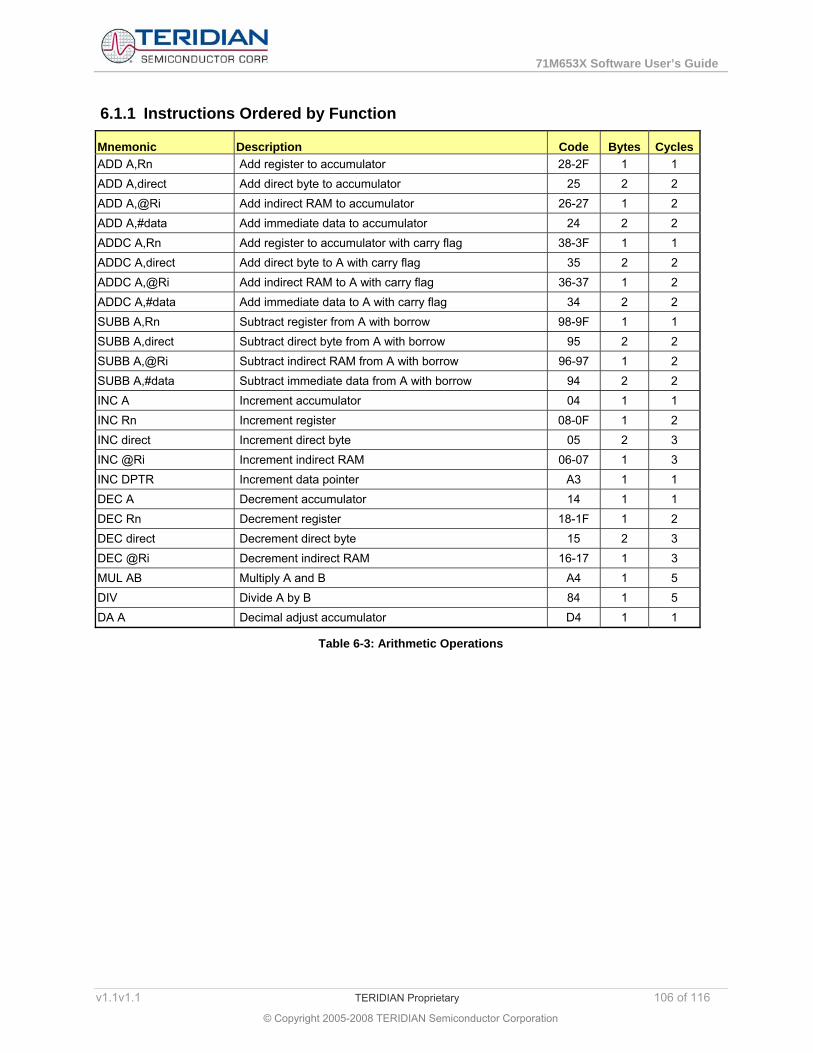
71M653X Software User’s Guide
6.1.1 Instructions Ordered by Function
Mnemonic Description Code Bytes CyclesADD A,Rn Add register to accumulator 28-2F 1 1 ADD A,direct Add direct byte to accumulator 25 2 2 ADD A,@Ri Add indirect RAM to accumulator 26-27 1 2 ADD A,#data Add immediate data to accumulator 24 2 2 ADDC A,Rn Add register to accumulator with carry flag 38-3F 1 1 ADDC A,direct Add direct byte to A with carry flag 35 2 2 ADDC A,@Ri Add indirect RAM to A with carry flag 36-37 1 2 ADDC A,#data Add immediate data to A with carry flag 34 2 2 SUBB A,Rn Subtract register from A with borrow 98-9F 1 1 SUBB A,direct Subtract direct byte from A with borrow 95 2 2 SUBB A,@Ri Subtract indirect RAM from A with borrow 96-97 1 2 SUBB A,#data Subtract immediate data from A with borrow 94 2 2 INC A Increment accumulator 04 1 1 INC Rn Increment register 08-0F 1 2 INC direct Increment direct byte 05 2 3 INC @Ri Increment indirect RAM 06-07 1 3 INC DPTR Increment data pointer A3 1 1 DEC A Decrement accumulator 14 1 1 DEC Rn Decrement register 18-1F 1 2 DEC direct Decrement direct byte 15 2 3 DEC @Ri Decrement indirect RAM 16-17 1 3 MUL AB Multiply A and B A4 1 5 DIV Divide A by B 84 1 5 DA A Decimal adjust accumulator D4 1 1
Table 6-3: Arithmetic Operations
v1.1v1.1 TERIDIAN Proprietary 106 of 116
© Copyright 2005-2008 TERIDIAN Semiconductor Corporation
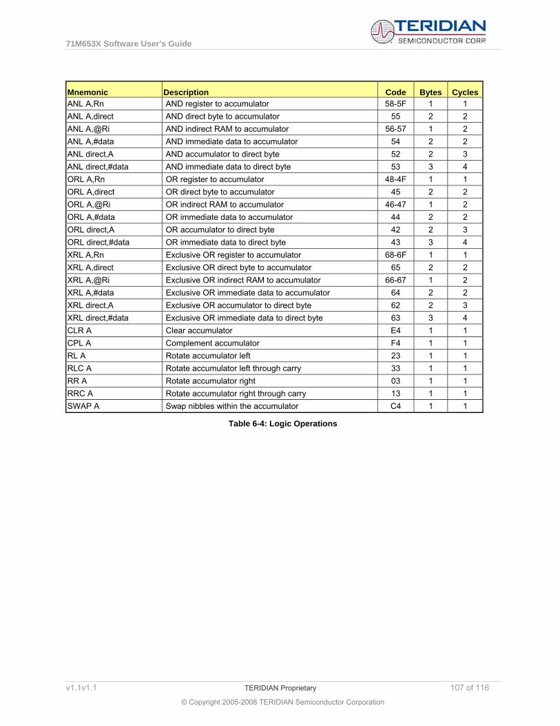
71M653X Software User’s Guide
Mnemonic Description Code Bytes CyclesANL A,Rn AND register to accumulator 58-5F 1 1 ANL A,direct AND direct byte to accumulator 55 2 2 ANL A,@Ri AND indirect RAM to accumulator 56-57 1 2 ANL A,#data AND immediate data to accumulator 54 2 2 ANL direct,A AND accumulator to direct byte 52 2 3 ANL direct,#data AND immediate data to direct byte 53 3 4 ORL A,Rn OR register to accumulator 48-4F 1 1 ORL A,direct OR direct byte to accumulator 45 2 2 ORL A,@Ri OR indirect RAM to accumulator 46-47 1 2 ORL A,#data OR immediate data to accumulator 44 2 2 ORL direct,A OR accumulator to direct byte 42 2 3 ORL direct,#data OR immediate data to direct byte 43 3 4 XRL A,Rn Exclusive OR register to accumulator 68-6F 1 1 XRL A,direct Exclusive OR direct byte to accumulator 65 2 2 XRL A,@Ri Exclusive OR indirect RAM to accumulator 66-67 1 2 XRL A,#data Exclusive OR immediate data to accumulator 64 2 2 XRL direct,A Exclusive OR accumulator to direct byte 62 2 3 XRL direct,#data Exclusive OR immediate data to direct byte 63 3 4 CLR A Clear accumulator E4 1 1 CPL A Complement accumulator F4 1 1 RL A Rotate accumulator left 23 1 1 RLC A Rotate accumulator left through carry 33 1 1 RR A Rotate accumulator right 03 1 1 RRC A Rotate accumulator right through carry 13 1 1 SWAP A Swap nibbles within the accumulator C4 1 1
Table 6-4: Logic Operations
v1.1v1.1 TERIDIAN Proprietary 107 of 116
© Copyright 2005-2008 TERIDIAN Semiconductor Corporation

71M653X Software User’s Guide
Mnemonic Description Code Bytes CyclesMOV A,Rn Move register to accumulator E8-EF 1 1 MOV A,direct Move direct byte to accumulator E5 2 2 MOV A,@Ri Move indirect RAM to accumulator E6-E7 1 2 MOV A,#data Move immediate data to accumulator 74 2 2 MOV Rn,A Move accumulator to register F8-FF 1 2 MOV Rn,direct Move direct byte to register A8-AF 2 4 MOV Rn,#data Move immediate data to register 78-7F 2 2 MOV direct,A Move accumulator to direct byte F5 2 3 MOV direct,Rn Move register to direct byte 88-8F 2 3 MOV direct1,direct2 Move direct byte to direct byte 85 3 4 MOV direct,@Ri Move indirect RAM to direct byte 86-87 2 4 MOV direct,#data Move immediate data to direct byte 75 3 3 MOV @Ri,A Move accumulator to indirect RAM F6-F7 1 3 MOV @Ri,direct Move direct byte to indirect RAM A6-A7 2 5 MOV @Ri,#data Move immediate data to indirect RAM 76-77 2 3 MOV DPTR,#data16 Load data pointer with a 16-bit constant 90 3 3 MOVC A,@A+DPTR Move code byte relative to DPTR to accumulator 93 1 3 MOVC A,@A+PC Move code byte relative to PC to accumulator 83 1 3 MOVX A,@Ri Move external RAM (8-bit addr.) to A E2-E3 1 3-10 MOVX A,@DPTR Move external RAM (16-bit addr.) to A E0 1 3-10 MOVX @Ri,A Move A to external RAM (8-bit addr.) F2-F3 1 4-11 MOVX @DPTR,A Move A to external RAM (16-bit addr.) F0 1 4-11 PUSH direct Push direct byte onto stack C0 2 4 POP direct Pop direct byte from stack D0 2 3 XCH A,Rn Exchange register with accumulator C8-CF 1 2 XCH A,direct Exchange direct byte with accumulator C5 2 3 XCH A,@Ri Exchange indirect RAM with accumulator C6-C7 1 3 XCHD A,@Ri Exchange low-order nibble indirect RAM with A D6-D7 1 3
Table 6-5: Data Transfer Operations
v1.1v1.1 TERIDIAN Proprietary 108 of 116
© Copyright 2005-2008 TERIDIAN Semiconductor Corporation
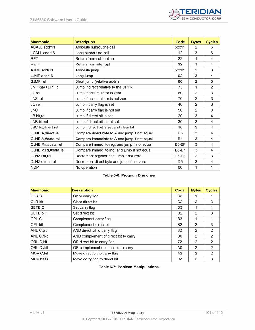
71M653X Software User’s Guide
Mnemonic Description Code Bytes CyclesACALL addr11 Absolute subroutine call xxx11 2 6 LCALL addr16 Long subroutine call 12 3 6 RET Return from subroutine 22 1 4 RETI Return from interrupt 32 1 4 AJMP addr11 Absolute jump xxx01 2 3 LJMP addr16 Long jump 02 3 4 SJMP rel Short jump (relative addr.) 80 2 3 JMP @A+DPTR Jump indirect relative to the DPTR 73 1 2 JZ rel Jump if accumulator is zero 60 2 3 JNZ rel Jump if accumulator is not zero 70 2 3 JC rel Jump if carry flag is set 40 2 3 JNC Jump if carry flag is not set 50 2 3 JB bit,rel Jump if direct bit is set 20 3 4 JNB bit,rel Jump if direct bit is not set 30 3 4 JBC bit,direct rel Jump if direct bit is set and clear bit 10 3 4 CJNE A,direct rel Compare direct byte to A and jump if not equal B5 3 4 CJNE A,#data rel Compare immediate to A and jump if not equal B4 3 4 CJNE Rn,#data rel Compare immed. to reg. and jump if not equal B8-BF 3 4 CJNE @Ri,#data rel Compare immed. to ind. and jump if not equal B6-B7 3 4 DJNZ Rn,rel Decrement register and jump if not zero D8-DF 2 3 DJNZ direct,rel Decrement direct byte and jump if not zero D5 3 4 NOP No operation 00 1 1
Table 6-6: Program Branches
Mnemonic Description Code Bytes CyclesCLR C Clear carry flag C3 1 1 CLR bit Clear direct bit C2 2 3 SETB C Set carry flag D3 1 1 SETB bit Set direct bit D2 2 3 CPL C Complement carry flag B3 1 1 CPL bit Complement direct bit B2 2 3 ANL C,bit AND direct bit to carry flag 82 2 2 ANL C,/bit AND complement of direct bit to carry B0 2 2 ORL C,bit OR direct bit to carry flag 72 2 2 ORL C,/bit OR complement of direct bit to carry A0 2 2 MOV C,bit Move direct bit to carry flag A2 2 2 MOV bit,C Move carry flag to direct bit 92 2 3
Table 6-7: Boolean Manipulations
v1.1v1.1 TERIDIAN Proprietary 109 of 116
© Copyright 2005-2008 TERIDIAN Semiconductor Corporation

71M653X Software User’s Guide
6.1.2 Instructions Ordered by Opcode (Hexadecimal)
Opcode Mnemonic Opcode Mnemonic Opcode Mnemonic 0x00 NOP 0x20 JB bit.rel 0x40 JC rel 0x01 AJMP addr11 0x21 AJMP addr11 0x41 AJMP addr11 0x02 LJMP addr16 0x22 RET 0x42 ORL direct,A 0x03 RR A 0x23 RL A 0x43 ORL direct,#data0x04 INC A 0x24 ADD A,#data 0x44 ORL A,#data 0x05 INC direct 0x25 ADD A,direct 0x45 ORL A,direct 0x06 INC @R0 0x26 ADD A,@R0 0x46 ORL A,@R0 0x07 INC @R1 0x27 ADD A,@R1 0x47 ORL A,@R1 0x08 INC R0 0x28 ADD A,R0 0x48 ORL A,R0 0x09 INC R1 0x29 ADD A,R1 0x49 ORL A,R1 0x0A INC R2 0x2A ADD A,R2 0x4A ORL A,R2 0x0B INC R3 0x2B ADD A,R3 0x4B ORL A,R3 0x0C INC R4 0x2C ADD A,R4 0x4C ORL A,R4 0x0D INC R5 0x2D ADD A,R5 0x4D ORL A,R5 0x0E INC R6 0x2E ADD A,R6 0x4E ORL A,R6 0x0F INC R7 0x2F ADD A,R7 0x4F ORL A,R7 0x10 JBC bit,rel 0x30 JNB bit.rel 0x50 JNC rel 0x11 ACALL addr11 0x31 ACALL addr11 0x51 ACALL addr11 0x12 LCALL addr16 0x32 RETI 0x52 ANL direct,A 0x13 RRC A 0x33 RLC A 0x53 ANL direct,#data 0x14 DEC A 0x34 ADDC A,#data 0x54 ANL A,#data 0x15 DEC direct 0x35 ADDC A,direct 0x55 ANL A,direct 0x16 DEC @R0 0x36 ADDC A,@R0 0x56 ANL A,@R0 0x17 DEC @R1 0x37 ADDC A,@R1 0x57 ANL A,@R1 0x18 DEC R0 0x38 ADDC A,R0 0x58 ANL A,R0 0x19 DEC R1 0x39 ADDC A,R1 0x59 ANL A,R1 0x1A DEC R2 0x3A ADDC A,R2 0x5A ANL A,R2 0x1B DEC R3 0x3B ADDC A,R3 0x5B ANL A,R3 0x1C DEC R4 0x3C ADDC A,R4 0x5C ANL A,R4 0x1D DEC R5 0x3D ADDC A,R5 0x5D ANL A,R5 0x1E DEC R6 0x3E ADDC A,R6 0x5E ANL A,R6 0x1F DEC R7 0x3F ADDC A,R7 0x5F ANL A,R7
Table 6-8: Instruction Set in Hexadecimal Order
v1.1v1.1 TERIDIAN Proprietary 110 of 116
© Copyright 2005-2008 TERIDIAN Semiconductor Corporation

71M653X Software User’s Guide
Opcode Mnemonic Opcode Mnemonic Opcode Mnemonic 0x60 JZ rel 0x80 SJMP rel 0xA0 ORL C,bit 0x61 AJMP addr11 0x81 AJMP addr11 0xA1 AJMP addr11 0x62 XRL direct,A 0x82 ANL C,bit 0xA2 MOV C,bit 0x63 XRL direct,#data 0x83 MOVC A,@A+PC 0xA3 INC DPTR 0x64 XRL A,#data 0x84 DIV AB 0xA4 MUL AB 0x65 XRL A,direct 0x85 MOV direct,direct 0xA5 Reserved 0x66 XRL A,@R0 0x86 MOV direct,@R0 0xA6 MOV @R0,direct 0x67 XRL A,@R1 0x87 MOV direct,@R1 0xA7 MOV @R1,direct 0x68 XRL A,R0 0x88 MOV direct,R0 0xA8 MOV R0,direct 0x69 XRL A,R1 0x89 MOV direct,R1 0xA9 MOV R1,direct 0x6A XRL A,R2 0x8A MOV direct,R2 0xAA MOV R2,direct 0x6B XRL A,R3 0x8B MOV direct,R3 0xAB MOV R3,direct 0x6C XRL A,R4 0x8C MOV direct,R4 0xAC MOV R4,direct 0x6D XRL A,R5 0x8D MOV direct,R5 0xAD MOV R5,direct 0x6E XRL A,R6 0x8E MOV direct,R6 0xAE MOV R6,direct 0x6F XRL A,R7 0x8F MOV direct,R7 0xAF MOV R7,direct 0x70 JNZ rel 0x90 MOV
DPTR,#data16 0xB0 ANL C,bit
0x71 ACALL addr11 0x91 ACALL addr11 0xB1 ACALL addr11 0x72 ORL C,direct 0x92 MOV bit,C 0xB2 CPL bit 0x73 JMP @A+DPTR 0x93 MOVC
A,@A+DPTR 0xB3 CPL C
0x74 MOV A,#data 0x94 SUBB A,#data 0xB4 CJNE A,#data,rel 0x75 MOV direct,#data 0x95 SUBB A,direct 0xB5 CJNE A,direct,rel 0x76 MOV @R0,#data 0x96 SUBB A,@R0 0xB6 CJNE @R0,#data,rel0x77 MOV @R1,#data 0x97 SUBB A,@R1 0xB7 CJNE @R1,#data,rel0x78 MOV R0.#data 0x98 SUBB A,R0 0xB8 CJNE R0,#data,rel 0x79 MOV R1.#data 0x99 SUBB A,R1 0xB9 CJNE R1,#data,rel 0x7A MOV R2.#data 0x9A SUBB A,R2 0xBA CJNE R2,#data,rel 0x7B MOV R3.#data 0x9B SUBB A,R3 0xBB CJNE R3,#data,rel 0x7C MOV R4.#data 0x9C SUBB A,R4 0xBC CJNE R4,#data,rel 0x7D MOV R5.#data 0x9D SUBB A,R5 0xBD CJNE R5,#data,rel 0x7E MOV R6.#data 0x9E SUBB A,R6 0xBE CJNE R6,#data,rel 0x7F MOV R7.#data 0x9F SUBB A,R7 0xBF CJNE R7,#data,rel
Table 6-9: Instruction Set in Hexadecimal Order
v1.1v1.1 TERIDIAN Proprietary 111 of 116
© Copyright 2005-2008 TERIDIAN Semiconductor Corporation
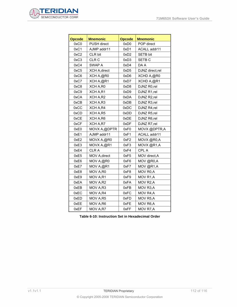
71M653X Software User’s Guide
Opcode Mnemonic Opcode Mnemonic 0xC0 PUSH direct 0xD0 POP direct 0xC1 AJMP addr11 0xD1 ACALL addr11 0xC2 CLR bit 0xD2 SETB bit 0xC3 CLR C 0xD3 SETB C 0xC4 SWAP A 0xD4 DA A 0xC5 XCH A,direct 0xD5 DJNZ direct,rel 0xC6 XCH A,@R0 0xD6 XCHD A,@R0 0xC7 XCH A,@R1 0xD7 XCHD A,@R1 0xC8 XCH A,R0 0xD8 DJNZ R0,rel 0xC9 XCH A,R1 0xD9 DJNZ R1,rel 0xCA XCH A,R2 0xDA DJNZ R2,rel 0xCB XCH A,R3 0xDB DJNZ R3,rel 0xCC XCH A,R4 0xDC DJNZ R4,rel 0xCD XCH A,R5 0xDD DJNZ R5,rel 0xCE XCH A,R6 0xDE DJNZ R6,rel 0xCF XCH A,R7 0xDF DJNZ R7,rel 0xE0 MOVX A,@DPTR 0xF0 MOVX @DPTR,A 0xE1 AJMP addr11 0xF1 ACALL addr11 0xE2 MOVX A,@R0 0xF2 MOVX @R0,A 0xE3 MOVX A,@R1 0xF3 MOVX @R1,A 0xE4 CLR A 0xF4 CPL A 0xE5 MOV A,direct 0xF5 MOV direct,A 0xE6 MOV A,@R0 0xF6 MOV @R0,A 0xE7 MOV A,@R1 0xF7 MOV @R1,A 0xE8 MOV A,R0 0xF8 MOV R0,A 0xE9 MOV A,R1 0xF9 MOV R1,A 0xEA MOV A,R2 0xFA MOV R2,A 0xEB MOV A,R3 0xFB MOV R3,A 0xEC MOV A,R4 0xFC MOV R4,A 0xED MOV A,R5 0xFD MOV R5,A 0xEE MOV A,R6 0xFE MOV R6,A 0xEF MOV A,R7 0xFF MOV R7,A
Table 6-10: Instruction Set in Hexadecimal Order
v1.1v1.1 TERIDIAN Proprietary 112 of 116
© Copyright 2005-2008 TERIDIAN Semiconductor Corporation

71M653X Software User’s Guide
6.1.3 Instructions that Affect Flags
Instruction Affected Flag Instruction Affected Flag
C OV AC C OV AC ADD X X X CLR C 0
ADDC X X X CPL C X SUBB X X X ANL C, bit X MUL 0 X ANL C, /bit X DIV 0 X ORL C, bit X DA X ORL C, /bit X
RRC X MOV C, bit X RLC X CJNE X
SETB C 1
Table 6-11: Instructions Affecting Flags
Note: Operations affecting the PSW or bits in the PSW will also affect flag settings
v1.1v1.1 TERIDIAN Proprietary 113 of 116
© Copyright 2005-2008 TERIDIAN Semiconductor Corporation

71M653X Software User’s Guide
v1.1v1.1 TERIDIAN Proprietary 114 of 116
© Copyright 2005-2008 TERIDIAN Semiconductor Corporation

71M653X Software User’s Guide
7 7 APPENDIX
7.1 ACRONYMS AC Alternating Current – current with changing polarity
AMR Automated Meter Reading, usually performed via an optical port or modem
ANSI American National Standardization Institution, part of ISO
ANSI C C Programming Language, standardized by ANSI in 1983. Keil C, used throughout this User’s Guide is not strictly ANSI compliant.
API Application Programming Interface
C The C Programming Language, as defined by Kernighan and Ritchie
CE Computation Engine
<CR> Carriage Return or Enter Key on PC Keyboard
COM Communication Port
CPU Control Processor Unit (MPU)
DC Direct Current
EEP Engineering Evaluation Platform (Demo Board)
EEPROM Electrically Erasable PROM
FLAG An international protocol for reading of meters using an optical port, initially developed by Ferranti and Landis&Gyr
GB Gigabyte(s)
ICE In-Circuit Emulator
IDE Integrated Development Environment – usually a combination of editor, compiler, assembler, linker, debugger, ICE
IEC International Electrotechnical Commission (Geneva, Switzerland)
INT Interrupt
ISO International Standards Organization
ISR Interrupt Service Routine
KB Kilobyte(s) – 1,024 bytes
LCD Liquid Crystal Display
<LF> Line-feed character
LSB Least Significant Bit
MB Megabyte(s) – 1,024 kilobytes
MPU Microprocessor/microcontroller Unit
v1.1v1.1 TERIDIAN Proprietary 115 of 116
© Copyright 2005-2008 TERIDIAN Semiconductor Corporation

71M653X Software User’s Guide
MSB Most Siginificant Bit
NV Non-Volatile
PC Personal Computer, Program Counter
PROM Programmable ROM
PSU Power Supply Unit
PSW Program Status Word
RAM Random Access Memory
ROM Read Only Memory
SFR Special Function Register (of the 8051 MPU)
TOU Time-of-Use (variable metering tariffs usually based on time of day)
TSC TERIDIAN Semiconductor Corporation
USB Universal Serial Bus
VA Volt-Amperes (apparent power unit)
VAh Volt-Ampere-Hour (apparent energy unit)
VAR Reactive Power
VARh Reactive energy unit
W Watt (power unit)
WD Watchdog
WDT Watchdog timer
WEMU51 The emulator control program by Signum Systems
Wh Watt-Hour (energy unit)
7.2 REVISION HISTORY
Revision Date Description 1.0 11-2-2007 Initial release
1.1 5-7-2008 Added useful excerpts from the SDD. Removed most of 80515 MPU core description (contained in data sheets), except op-code tables. Added description of Intel Hex File formats for regular and banked code.
Software User Guide: This User Guide contains proprietary product definition information of TERIDIAN Semiconductor Corporation (TSC) and is made available for informational purposes only. TERIDIAN assumes no obligation regarding future manufacture, unless agreed to in writing. If and when manufactured and sold, this product is sold subject to the terms and conditions of sale supplied at the time of order acknowledgment, including those pertaining to warranty, patent infringement and limitation of liability. TERIDIAN Semiconductor Corporation (TSC) reserves the right to make changes in specifications at any time without notice. Accordingly, the reader is cautioned to verify that a data sheet is current before placing orders. TSC assumes no liability for applications assistance.
TERIDIAN Semiconductor Corp., 6440 Oak Canyon Road, Suite 100, Irvine, CA 92618-5201 TEL (714) 508-8800, FAX (714) 508-8877, http://www.teridian.com
5/8/2008
v1.1v1.1 TERIDIAN Proprietary 116 of 116
© Copyright 2005-2008 TERIDIAN Semiconductor Corporation