empower - ucf department of eecs · 1.1 project motivation …………………………… ......
TRANSCRIPT

eMpower Solar Powered mobile device
charger with remote control
Members Group 32 Kellman Pryor, Anjanett Exum, Stephen Sheldon, Bernard Feeser
Sponsors Water Missions International, Progress Energy

ii
Table of Contents Page
1. Executive Summary …………………………………..………………… 1 1.1 Project Motivation ………………………………..………………… 2 2. Project Requirements and Specifications …………….………………... 3 2.1 Water Mission Specifications ………………………………………. 4 2.2 Robustness and Safety ……………………………………………… 5
2.3 Serviceability ………………………………………………………… 6
3. Research Related to Project Definition …………………………………. 8 3.1 Existing Similar Project/Products …………………………………… 8 3.1.1 GSM/GPRS Controlled Devices ………………………………… 8 3.1.1.1 Past Senior Design Projects ………………………………… 9 3.1.1.2 Current Hardware …………………………………………… 9 3.1.2 Mobile Device Charging Kiosk …………………………………. 12 3.1.3 Phone Chargers ………………………………………………….. 14
3.2 GSM/GPRS Research ………………………………………………. 16 3.2.1 GSM GPRS Requirements ……………………………………… 16 3.2.2 GSM/GPRS Device Comparison ………………………………. 17 3.2.2.1 Telit GE865-QUAD …………………………………………. 19 3.2.2.2 SIMCom SIM900 ……………………………………..……. 20 3.3 Power Regulation Research ………………………………………… 25 3.3.1 Primary Power Distribution ………………………………. ….. 25 3.3.2 Secondary Power distribution …………………………………. 30 3.4 Central Processor/Controller Research ……………………………. 31 3.4.1 PIC Microcontrollers …………………………………………… 32 3.4.2 MSP430 Microcontrollers ……………………………………... 34 3.4.3 Parallax Propeller Microcontrollers ……………………………. 36 3.4.4 Atmel ATmega Microcontrollers ………………………………. 37 3.4.5 Microcontroller Choice …………………………………………. 40 3.5 User Interface Research …………………………………………….. 40 3.5.1 Grayhill 4x4 Switch Keypad Research …………………………. 41 3.5.2 LCD Screen ………………………………………………………. 44 3.5.3 Visual Display Research ………………………………………… 45 3.5.3.1 Sharp TFT-LCD …………………………………………….. 45 3.5.3.2 Longtech Optics LCD Display ………………………………. 46 3.6 Non-Volatile Memory Storage Research ……………………………. 48 3.6.1 MicroSD Card Interface …………………………………………. 48 3.7 Charging port Control Research ………………………………. ……. 49 3.7.1 Port Power Control ……………………………………………… 49 3.7.2 Secondary Microcontroller Research ……..……………………. 51 3.7.3 Intersystem Communication ………………………………. …… 54 4. Project Hardware / Software Design Details ……………………………. 56
4.1 Hardware Design ……………………………………………………. 56
4.1.1 Master Unit ……………………………………………………… 57
4.1.1.1 Primary Power Supply …………………………………….. 58

iii
4.1.1.2 Secondary Power Supply ……………………………………. 61 4.1.1.3 Main Communications System Design ……………………… 62 4.1.1.4 GPRS Shield …………………………………………………. 65 4.1.1.5 Keypad ………………………………………………………. 65 4.1.1.6 LCD Display ………………………………………………… 65 4.1.1.7 SD Card ……………………………………………………… 65 4.1.2 Slave Unit ………………………………………………………… 66
4.2 Software Design ……………………………………………………… 68
4.2.1 User Interaction Workflow ……………………………………… 68 4.2.2 Interface State Diagram …………………………………………. 73 4.2.3 GSM/GPRS Communications Software Workflow ……………… 75 4.2.3.1 Remote SMS Receiving ……………………………………… 76 4.2.3.2 Command Execution Confirmation ………………………… 77 4.2.3.3 Command Execution Testing ………………………………. 78 4.2.4 Software Design Summary of Communications Board …………. 79 4.2.5 GSM Shield Library ……………………………………………… 80 4.2.6 Keypad Library …………………………………………………… 82 4.2.7 SD Card Library …………………………………………………. 83 5. Parts Acquisition ………………………………………………………… 83 5.1 Parts Lists ……………………………………………………………. 84 5.2 BOMs ………………………………………………………………… 85 6. Project Prototype Testing ………………………………………………… 97 6.1 Hardware Specific Testing …………………………………………... 97 6.2 Software Specific Testing …………………………………………… 98 6.2.1 Phase One – With development board …………………………. 98 6.2.1.1 Keypad Only ………………………………………………… 98 6.2.1.2 LCD Only ……………………………………………………. 100 6.2.1.3 GSM/GPRS Module Only ………………………………….. 101 6.2.1.4 Keypad/LCD/GSM Together ………………………………. 101 6.2.1.5 Server Side Testing …………………………………………. 103 6.2.1.6 SD Card Storage Testing …………………………………… 104 6.3 Testing Protocols ……………………………………………………. 104 7. Administrative Content …………………………………………………. 119 7.1 Turnover to Water Missions ……………………………………….. 122 7.2 Budget and Finance Discussion ……………………………………. 124 7.2.1 Budget Sheet Breakdown ………………………………………. 125 Appendix A …………………………………………………………………. I Appendix B …………………………………………………………………. XIII
iv
Table of Figures
Figure 1 Open Electronics GSM Remote Control – 2 IN and 2 OUT .............................. 11
Figure 2 Rocket Scream’s TraLog Schematic .................................................................. 12
Figure 3 GoCharge’s Themis Free standing charging kiosk ............................................ 14
Figure 4 NV3 Technologies’ NTC-1912 Cell phone charging kiosk ............................... 14
Figure 5 Brightbox charging kiosk ................................................................................... 15
Figure 6 Apple Charging Unit .......................................................................................... 16
Figure 7 Apple iphone Charger Schematic ....................................................................... 16
Figure 8 GSM Network Structure .................................................................................... 19
Figure 9 Sparkfun GE865 Breakout Board Schematic ..................................................... 20
Figure 10 SIMCom Sim900 Breakout Board from Open Electronics ............................. 21
Figure 11 SIM900 Breakout Board from Open Electronics ............................................. 22
Figure 12 GSM/GPRS Shield Schematic from Open Electronics .................................... 23
Figure 13 GSM/GPRS Shield from Open Electronics ...................................................... 24
Figure 14 Seeed Studio GPRS Shield ............................................................................... 24
Figure 15 Seeed Studio GPRS Shield Schematic ............................................................. 25
Figure 16 Buck Controller Topology ................................................................................ 28
Figure 17 Buck-Boost Controller Topology ..................................................................... 28
Figure 18 SEPIC Controller Topology ............................................................................. 29
Figure 19 Flyback Controller Topology .......................................................................... 30
Figure 20 Forward Controller Topology........................................................................... 30
Figure 21 PIC18F8723 Functional Diagram..................................................................... 34
Figure 22 MSP430F2619 Functional Diagram ................................................................. 36
Figure 23 MSP430F5438A Function Diagram ................................................................. 36
Figure 24 Propeller P8X32A-Q44 Functional Diagram ................................................... 38
Figure 25 ATmega328P-PU Functional Diagram ............................................................ 39
Figure 26 ATmega2560-16AU Functional Diagram ........................................................ 40
Figure 27 Front view of charging unit showing location of LCD and keypad ................. 42
Figure 28 Grayhill 4x4 Keypad Layout ............................................................................ 43
Figure 29 Grayhill 4x4 Keypad ........................................................................................ 44
Figure 30 Grayhill Series 86 4x4 Keypad Terminations and Truth Table ...................... 44
Figure 31 LCM2004SD-NSW-BBW 20x4 LCD .............................................................. 45
Figure 32 LCD Screen layout ........................................................................................... 46
Figure 33 Pin layout .......................................................................................................... 46
Figure 34 Sharp TFT-LCD Display .................................................................................. 47
Figure 35 Longtech Optics LCD Display ......................................................................... 48
Figure 36 Adafruit microSD breakout board. ................................................................... 50
Figure 37 Application circuit of TPS2511 ........................................................................ 52
Figure 38 I2C Addressing Circuit ..................................................................................... 56
Figure 39 Master Unit Block Diagram ............................................................................. 58
Figure 40 Primary Power Supply First Stage ................................................................... 62
Figure 41Primary Power Second Stage Schematic ........................................................... 63
Figure 42 Secondary Power Schematic ............................. Error! Bookmark not defined.
Figure 43 Schematic of Main Communications Module .................................................. 65

v
Figure 44 Mega2560 USB Interface ................................................................................. 65
Figure 45 Pin Mapping of Arduino Mega......................................................................... 66
Figure 46 Slave Unit Block Diagram................................................................................ 69
Figure 47 Sample Client Account ..................................................................................... 71
Figure 48 Initial menu for phone number ......................................................................... 72
Figure 49 Initial menu for pin number .............................................................................. 72
Figure 50 Main Menu setting up port ............................................................................... 73
Figure 51 Main Menu checking minutes .......................................................................... 74
Figure 52 Main Menu choosing to exit ............................................................................. 75
Figure 53 Device side state diagram ................................................................................. 76
Figure 54 Client side state diagram .................................................................................. 77
Figure 55 Initial SMS Receiving Workflow ..................................................................... 79
Figure 56 Command Execution Confirmation Flow Chart ............................................... 80
Figure 57 Command Execution Testing Flow Chart ........................................................ 81
Figure 58 Keypad configuration ....................................................................................... 92
Figure 59 Output on LCD with four lines ......................................................................... 94
Figure 60 LCD Splash Screen ........................................................................................... 95
Figure 61 Printout of Account Totals ............................................................................... 96

vi
Table of Tables
Table 1 PIC18F8723 Specifications ................................................................................. 33
Table 2 MSP430 Microcontroller Specifications ............................................................. 35
Table 3 Propeller Microcontroller Specifications ............................................................. 37
Table 4 ATmega Microcontroller Specifications ............................................................. 39
Table 5 DC Characteristics of Longtech Display ............................................................. 49
Table 6 Port control unit MCU I/O quantity determination ............................................. 53
Table 7 MCU Comparison Chart ...................................................................................... 54
Table 8 First stage specifications ....................................... Error! Bookmark not defined.
Table 9 Second stage specifications ................................................................................. 62
Table 10 Secondary Power stage specifications ............................................................... 64
Table 11 Table of some of the available SMS functions of the GSMSHIELD library .... 82
Table 12 Table of some of the available GPRS functions of the GSMSHIELD library .. 83
Table 13 Master Unit Parts List ........................................................................................ 86
Table 14 Slave Unit Parts List .......................................................................................... 86
Table 15 Primary Power Supply BOM .............................. Error! Bookmark not defined.
Table 16 Secondary Power Supply BOM .......................... Error! Bookmark not defined.
Table 17 Communication Control BOM .......................................................................... 87
Table 18 Central Control BOM ........................................................................................ 88
Table 19 Charge Port Control BOM ................................................................................. 89
Table 20 Fall 2012 Breakdown .......................................... Error! Bookmark not defined.
Table 21 Spring 2013 Breakdown ..................................... Error! Bookmark not defined.
Table 22 Mobile Charging Device Budget ..................................................................... 106
1
1.1 Executive Summary
The eMpower solar powered mobile device charger is a device that provides a safe way for remote water pump stations to provide mobile device charging capabilities. The sponsor, Water Missions International (www.watermissions.org) is a nonprofit organization that focuses on creating safe water and sanitation systems for people in developing countries. More often than not these water treatment systems include solar panels to power the pumps. Water Missions’ engineers typically oversize the solar panel array so that there will be enough power to run the water treatment system under different weather conditions. A few months ago an operator of one of Water Missions’ systems wired a power strip in parallel with the pump and plugged in cell phone chargers to start charging cell phones. Surprisingly, his set up worked and his business has been quite successful, charging dozens of phones per day. The charging business is so successful that it is bringing in more income than the water sales. The eMpower device introduces a safer setup as well as features that will allow Water Missions International to control the device remotely. Given the specifications from Water Missions International, the team proceeded to design a device with the following primary objectives.
- Provide a mobile device charging interface using USB ports - Provide an account management interface to include local and remote
management trough SMS. - Provide a unit that can be reproduced with minimal cost per complete unit.
Secondary objectives to the projects will be to include a wide input power supply in order to seamlessly integrate with all Water Missions International project sites. Another secondary objective is to provide an expandable mobile device charging interface that connects to the main unit, and is expandable to multiple “slave” units. Car charging ports and diagnostics features will also be secondary objectives.
The team researched several topologies and components in order to provide circuits that would not only meet the specifications, but also provided cost effective options in order to keep the final price of the device under the minimum price range of $100. Using a dual stage buck and fly back converter, the primary power input is converted to the necessary voltages that will be needed throughout the device. The charge port module will route and switch the required 5 and 12 VDC to the individual ports to charge the mobile devices. The charge port module will also communicate the status of each port to the central processor. The central processor will communicate via SMS to the server several commands and logs, as well as determine which port the user will use. The central processor will also turn on and off each port as necessary and log the time each account uses. It will also send the command to turn off a port when the time on the account is exhausted.

2
The unit is specified to have a pre-determined number of ports per master unit. A slave unit will also be designed in order to allow for the expansion of charging capabilities. The central processor will detect the presence of the slave unit or units and employ the use of the added ports in the decision making scheme for users phone charging.
1.2 Project Motivation
According to the World Health Organization, an estimated 780 million people lack access to safe drinking water in 2010, and that number is rapidly growing. It appears that a lack of funding and motivation of getting filtration systems and pumps installed in areas of need is the reason why so many people remain deprived of this essential need. The real problem is that an estimated 30% of all hand pumps installed in sub-Saharan Africa over the past two decades have failed prematurely and water points in some areas such as the Chikwawa and Phalombe districts of Malawi are less than 50% functional. We initially contacted Water Missions International to see if they had any available projects that we could work on. They proposed that we help create a solution to their problem by creating a mobile phone device charging system that can be remotely monitored and controlled over a GSM and GPRS network. This device will be applicable to not only Water Missions Internationals project but to various other projects. Our goal is to design a safe, scalable product that has expandable features that can be deployed on Water Missions International’s and many other renewable energy project sites. Since Water Missions International is a nonprofit organization who must fundraise every dollar that is spent, affordability of these units while meeting the requirements is very important. While looking at the possible solutions, being cost-effective and creative is highly encouraged during the solution creation process. The result of this project being able to create revenue for Water Missions or any other organization is a real motivator on the sustainability of the project. This will allow people that do not have access to receive power at a nominal fee, and this fee will make sure that the project can endure for many years. This was important due to the increasing numbers of projects that are sitting dormant in other countries due to their lack of ability to be sustainable. This device will be able to be attached to any device that is set up to get sustainable power like a wind turbine, solar array, or any other project that produces power. That means that eMpower will make use of any lost power from other systems that aren’t put to use.
2. Project Requirements and Specifications

3
The following specifications are put forth by the Water Missions group. They are a list of specifications of the final field worthy unit that Water Missions wishes to employ in their many field locations alongside their solar water pumps. After thorough research, portions of the desired specification were eliminated in order to conform to the desired price point. Some features were not implemented but rather provisions for the feature were implemented in order to allow Water Missions the flexibility to add the desired feature in future revisions of the product.
2.1 Water Mission Specifications
The input voltages are a best estimate by the Water Missions group and are based off of the output voltages of their solar array that is already in place for their solar water pumps. The final project will include all the hardware and software needed to complete the solar charging unit but will not be turned over as a field ready device. It will rather be turned over as an advanced prototype model for future expansion. The expanded device will then be used to clone and deploy to the field. Due to the nature of solar arrays the range of input voltage is varying depending on if the sun is out or only partially exposed to the array.
• Charge attached devices with a fluctuating supply voltage range of 12-240 VDC.
Goal: (12-300 VDC)
• There will be 10 USB 2.0 type A sockets for charging at 5 V DC (up to 0.5 A
each)
• There will be an additional port where a hub can be plugged into to another 10
USB type A sockets. The hub will have an additional port where another hub can
be plugged into, so they are daisy-chained. This hub’s circuit board will also be
required to be designed and priced as an option.
• There will be 2 different cigarette lighter socket ports for 12 V outputs (up to 5 A
each).
• There will be some type of resettable fuse to protect too much current from being
drawn from each USB and cigarette lighter port
• Each port will have an LED to indicate the status of whether the port is charging
or not
• There will be two leads for an external battery (12-24V) that can be attached. This
battery will power the unit when solar power is not available but will not allow
the mobile devices to be charged through it.
• If power is lost while this unit is operating and the external battery is not attached,
when power is available again, the unit will automatically resume its normal
functionality (as well has having the correct date and time)

4
• The cumulative energy (kWh) used in charging the mobile devices’ batteries will
be logged at a configurable interval with a date and time stamp
• The cumulative energy used and a date time stamp will be sent through an
integrated Quad band GSM device (SMS or GPRS, you can help decide) to a
configurable cell phone number/domain at a configurable interval (daily, weekly
or monthly at noon). Multiple energy and date and time stamps will be sent per
message/packet.
• The Quadband GSM device can receive commands through SMS to configure and
control the unit. The following commands are required:
o Command to turn all charging ports on or off. This command can be used
through a reset command
o Command to send a custom text message (for entering the code to add
credit to prepaid SIM card in the unit) It can be used to update the account
of a client.
o There will be a prepaid option of adding energy credit to the unit. This
amount of energy credit is added by a SMS command. The unit will be
powered on as long as the energy credit is more than the value of the
energy sold. Once the unit’s credit is used up, then the unit disables
charging and sends a SMS notification (up to 4 phone numbers). When
more credit is added, then charging is enabled, until the credit is used up
again, then charging is disabled.
o Command to enable an alert to send an SMS to a configurable phone
number (up to 4 different phone numbers) when available energy (kWh)
credit is below a configurable value. If there is not any phone numbers
entered, SMSs are not sent. This command will be separate from a SMS
message to the client’s cell phone in order to alert the client of stats due to
their activity on their account.
o Command to configure the energy credit difference when a low
notification notice is sent
o Command to query how much energy credit is available on the unit in
reference to each client’s account
o Command to query the cumulative energy used with date time stamp on
the unit. It will return the total amount of energy granted to the clients’
accounts
o Command to update the interval (in minutes) how often the cumulative
energy used is logged into memory
o Command to query the date and time. The format will be in the order of
month, day, and year

5
o Command to update the date and time to the current time in case of
different time zones
o Command(s) to update where the SMS sends to (this includes up to 4
different phone numbers) or GPRS connects to (APN settings, domain,
protocol, etc.) to track where messages were sent and to where these
messages are sent
o Command to update the reporting frequency of cumulative kWh (daily,
weekly or monthly) This will require for a ongoing compiling or resources
and retrieval of this data.
o Command to update the unit’s ID number so that no two units will have
the same number for polling reasons
o Each command will have a success or failure reply message. That will
return a 1 for success or a 0 for failure of transmission in order to check
the validity of the results
o Each command will need a correct password entered before the command
is run. This password will precede the command and be in the same SMS.
There will be a different password for querying data and configuring the
unit. Unrecognized SMS will be ignored.
o Command to update the passwords for the overall security of the system
and protection of the clients’ accounts
o Command to query all the settings on the unit for status and reporting
format to include setting follow by the status of that setting where each
setting in separated by a blank line
• There will be a way to determine and troubleshoot the unit when there are
configuration issues and the unit can’t connect to the cell phone network. This is
not specified and can be determined by the completion team. It could be through a
hard wire to the unit itself.
• There will be a ON and OFF switch for the unit. This switch should not be easily
accessed by the clients.
• There will be a LED to show when the unit has power (on when there is power,
off when there is not any power)
• There will be a LED to show when charging ports are enabled because there is
sufficient energy credit (on when enabled, off when disabled) There can be a
color or flashing to determine the state of the port where it could be green when
on and red when off, If the account is nearing the end of its time or minutes
allowed the LED could blink
• The unit will be operated within the temperature range 0—45 degrees C, this is 0
– 113degrees F
• The unit will be stored in within the temperature range -20—60°C, this is -4 – 140
degrees F

6
2.2 eMpower Specifications
• Charge attached devices with a supply voltage range of 30 VDC.
• There will be 10 USB 2.0 type A sockets for charging at 5 V DC (up to 0.5 A
each)
• There will be an additional port where a hub can be plugged into to another 10
USB type A sockets. The hub will have an additional port where another hub can
be plugged into, so they are daisy-chained. This hub’s circuit board will also be
required to be designed and priced as an option.
• There will be 2 different cigarette lighter socket ports for 12 V outputs (up to 2A
each).
• Each port will have an LED to indicate the status of whether the port is charging
or not
• There will be provisions for an external battery (12-24V) that can be attached.
This battery will power the unit when solar power is not available but will not
allow the mobile devices to be charged through it. If power is lost while this unit
is operating and the external battery is not attached, when power is available
again, the unit will automatically resume its normal functionality.
• The Quadband GSM device can receive commands through SMS to configure and
control the unit. The following commands are required:
o Command to turn all charging ports on or off. This command can be used
through a reset command.
o Command to configure the time credit difference when a low notification
notice is sent.
o Command(s) to update where the SMS sends to (this includes up to 4
different phone numbers).
o Command to update the unit’s ID number so that no two units will have
the same number for polling reasons
o Each command will have a success or failure reply message. That will
return a 1 for success or a 0 for failure of transmission in order to check
the validity of the results
o Each command will need a correct password entered before the command
is run. This password will precede the command and be in the same SMS.
There will be a different password for querying data and configuring the
unit. Unrecognized SMS will be ignored.
o Command to update the passwords for the overall security of the system
and protection of the clients’ accounts

7
• There will be a way to determine and troubleshoot the unit when there are
configuration issues and the unit can’t connect to the cell phone network.
• There will be an ON and OFF switch for the unit.
• There will be a LED to show when charging ports are enabled because there is
sufficient energy credit (on when enabled, off when disabled) There can be a
color or flashing to determine the state of the port where it could be green when
on and red when off, If the account is nearing the end of its time or minutes
allowed the LED could blink
• The unit will be operated within the temperature range 0—45 degrees C, this is 0
– 113degrees F
• The unit will be stored in within the temperature range -20—60°C, this is -4 – 140
degrees F
2.4 Robustness and Safety
The robustness of the system is imperative due the nature of it providing and managing a
service that has financial implications to its users. The system must have a high uptime
ratio in order for the user to justify the expense of using the service. High quality
components with a long history of application and verified performance should be used in
the implementation of your design. Manufacture example application circuits should be
referenced where possible to reduce unexpected results in the field and reference designs
should be consulted when available.
User safety should be regarded as the primary design consideration. This system will be
located in remote villages where the equipment may be exposed to the elements. Users
are not expected to identify hazards or safety concerns and must not be allowed contact
with hazardous parts. The specific users of this system have little to no experience with
electricity and may not have the same regard for the potential danger of an unmaintained
or damaged electrical system as would a user from a society where electrical devices are
used on a daily basis. Grounding, lightning protection, moisture protection, and isolation
should be properly implemented. In regards to safety, ANSI/ISA S82.01 and ICASA’s
(Independent Communications Authority of South Africa) “Regulations in Respect of
Technical Standards for Electronic Communications Equipment” should be followed as
the final design will be used daily by the general population. Electric shock is not the
only aspect of electrical equipment safety design.

8
Fire hazards and burns result when equipment is not designed correctly, overloaded,
malfunctioning, or is not provided with proper heat dissipation. Thought must also be
given to the mechanical design of the unit. Injury or damage resulting from contact with
sharp edges or corners of the unit, movable parts, or being improperly secured or
mounted should be avoided at all times. Likely faults, power surges, and foreseeable
misuse should all be considered.
In order to protect attached devices, as well as the eMpower unit from damaged attached
devices, each charging port should be individually protected. The system should protect
against EMF noise caused by the connecting and disconnecting of devices as well as the
environment.
2.5 Serviceability
Serviceability must be considered in the design process to permit the operators to be able
to safely and reliably troubleshoot, repair, and expand the system. The specification
provided by Water Missions International requires that the unit be fitted with LEDs to
indicate when the unit has sufficient power. In the event that the unit shuts down, this
will provide the operator with an indication of whether proper power is simply not being
supplied by the power source, or if a malfunction has occurred and the unit its self is in
need of service.
Additionally, the provided specification calls for a system power switch that will be
incorporated in the system, which the operator may utilize to power down the unit. The
unit may be powered down in order to:
• Safely service the unit
• Reset the unit in the event of a malfunction
• Eliminate load on the power supply system
• Power off unit when not in service
Particular consideration to safety should be given in the design of how the unit will be
serviced. Since the unit will have a power supply of up to 30 volts the system should be
designed so that the switch shuts off power on the high potential voltage side of the
circuit in order to reduce or eliminate the risk of electrical shock. Any conductors within
the enclosure that have the capability of electrical shock should be properly insolated and
protected to prevent accidental contact. Capacitors that can have a discharge time greater

9
than several seconds should be protected against accidental shorting or contact. The
switch should also completely eliminate all loads to the primary power supply, in order to
provide the maximum amount of power to the water pump system in times of high
demand.
While not detailed in the provided specification, the system should be designed in a way
that it can be safely and easily serviced by the average individual that will be in charge of
daily management and upkeep the unit. The remote nature of the sites where these units
will be installed can hinder timely response of experienced support personnel. We
assume the primary servicer is proficient in the use of basic hand tools and has some
experience with several common types of electrical connectors. We assume no electronic
troubleshooting skills. In order to simplify the serviceability of the system in the event of
component malfunction, the units various subsystems should be designed and constructed
into several separate components, hereafter referred to “boards”. The various boards will
be:
• Main Board (1 per site)
• Power Supply Board (1per unit)
• Port Control board (1 per Unit)
If more charging ports are required at a later time, or if a unit is in need of replacement,
the master unit will automatically detect and configure expansion units each time it
powers up. This will eliminate the need of any onsite software configuration or
addressing as the system is expanded. The power regulator boards and charging port
boards that are found in all units should be standardized and interchangeable. All parts
should be labeled with dates and some sort of identification, such as a part number, so
that if any components of the system are redesigned at a later time, correct replacement
parts can be obtained without confusion.
Basic troubleshooting procedures and self-diagnostic tests should be provided to the
servicer to aid in assessing system malfunctions. Certain diagnostic tests are required to
have the ability to be performed remotely via the cellular communications system as
described in the administrative menu description portion of this document.
3. Research Related to Project Definition

10
The following is a compilation of the research of components that are included in the device including existing similar Projects and Products and research of technology and hardware.
3.1 Existing Similar Project/Products
It was found that the research of a similar device is very useful in the development of a final product. The fact that a similar device is a proven concept assisted directly with the design of the eMpower unit.
3.1.1 GSM/GPRS Controlled Devices
When initially researching what it would take to meet the requirements of this project it was important to consider what other people had done that was similar in the past. Several former Senior Design projects at the University of Central Florida have included GSM support, such as, Child and Pet Safety Notification System from Fall 2007 and The LiteBike from Spring 2011.
3.1.1.1 Past Senior Design Projects
The Child and Pet Safety Notification System was made to detect when a child or animal is in a vehicle and notify the owner when the inside temperature of the vehicle reaches levels considered hazardous to either the child or animal. GSM technology was incorporated in this project by using a GSM module in order to send an ‘alarm’ text to notify the owner of the vehicle once the motion detector detects movements and the temperature sensor detects unsafe temperature levels. This group used a Telit GM862-GPS GSM module along with an evaluation board from Spark fun. The LiteBike was a Senior Design project that was aimed at creating a safer bike by providing more visibility at night via a four part lighting system. It also incorporated a three-tier security system in order to prevent theft. Bike owners are to be alerted through text messages if the bike is potentially being stolen. GSM was also used to communicate GPS coordinate to the bike owner so that the owner could track the bike at any given time. This group used a Telit GE865 along with a breakout board developed by Sparkfun. This specific group decided to choose a Parallax Propeller microcontroller to communicate with their GSM module.

11
3.1.1.2 Current Hardware
Current hardware exists for the purposes of remotely controlling electrically controlled units and also acquiring data from electronic sensors. Open Electronics offers several GSM remote control development boards. One particular offering is a 2-in 2-out GSM remote control. It is powered by a PIC18F46K20-I/PT and contains two relays. This product was designed to interface with a SIMCOM900 GSM/GPRS module; taking commands from the module and sending commands to the two relays connected to the device. The schematics for this particular board can be seen below in Figure 1.
Figure 1 Open Electronics GSM Remote Control – 2 IN and 2 OUT
Reprinted from www.Open-Electronics.org

12
Another board that incorporates similar features as to what this project’s requirements are is the TraLog developed by Rocket Scream. Unlike the previous examples this board incorporates a microSD interface on it as well. It uses a Sierra Wireless WISMO228 GSM/GPRS module. The schematic for this particular board can be seen in Figure 2 below.
Figure 2 Rocket Scream’s TraLog Schematic
Reprinted with permission from www.rocketscream.com

13
3.1.2 Mobile Device Charging Kiosk
Mobile charging kiosk are gaining popularity in many venues where cellular device users
may be without access to a wall outlet for an extended period of time such as
conferences, universities, theme parks , and airports. These devices are also being used
in locations where cellular device users may likely be in need of a charge but there isn’t a
place to charge them such as lounges and bars. Some of the devices most prevalent in the
market are:
• Bright Box
• NV3 Technologies
• Go Charge
Most of these charging kiosks either allow users to charge their devices for free and profit
from advertising content presented on a screen mounted on the unit, or use a credit card
billing system. The latter utilize 3rd party cellular credit card processors that take care of
all communication services. No user account information is stored on these units,
simplifying their operation and reducing the liability of maintaining account balance
information.
These units are powered either by a standard AC service, or by a dedicated, fixed output
solar array. This eliminates the need for complicated and expensive wide range power
input conditioning. Many of these units are fitted with hardened 12” to 18” color touch
screens to provide user interface. These large color screens allow instructions to be
presented to the users along with images to make the users understanding as clear and
simple as possible.
To provide physical security to the user’s device while it is being charged, lockable
compartments are often provided to the customer. These lockers are unlocked by
entering a previously entered pin number or by swiping the same card on which the fee
was paid. The cardholder’s name, which is encoded on the magstrip of the card, is used
so that the credit card number does not need to be stored within the unit, increasing
security.

14
Figure 3 GoCharge’s Themis Free standing charging kiosk
Reprinted from: http://gochargenow.com/products.cfm?pid=106&ref=themis
permission pending
Figure 4 NV3 Technologies’ NTC-1912 Cell phone charging kiosk
Reprinted From: http://nv3tech.com/pc/products.php#ntc1912 permission pending

15
Figure 5 Brightbox charging kiosk
Reprinted From: http://nv3tech.com/pc/products.php#ntc1912 permission pending
3.1.3 Phone Chargers
Each mobile device manufacture supplies a charger that is recommended with their device. In recent years, most manufactures have moved toward standardization of their charging ports. Most mobile devices not only need a way to charge the battery, but also a way to transfer data to a computer. The USB architecture was chosen as the standard for this data transfer. USB 2.0 permitted 500mA to be provided to each port. As mobile devices demand more and more power, and battery capacity increases to meet those demands, 500 mA is becoming increasing insufficient and leads to long charge times. In an effort to reduce this charge time a number of originations have been involved in creating special charging previsions for the standard. The “USB-IF” and “OMTP” have the two most highly regarded standards. Some mobile platforms, like the Apple line of products, use a proprietary plug on the mobile device side of the connection cord. The ability to charge from a USB port is almost always supported by the use of a charging cable with the perspective ends. Apple implements some more sophisticated circuit protection that provides the ability for it to further determine the capabilities of the supplying device. This additional circuitry prevents Apple devices from being able to be charged on non-compliant devices that draw higher than 500mA. Ultimately we will examine an apple branded charger in order to reference our charging circuit from.
A comparison of the careful design and quality of components found in Apple’s iPhone charger to that of a standard aftermarket phone charger reveal the high importance that Apple has placed on providing proper current and clean voltage to their devices. Apple has implemented a switching power supply that operates around 70KHz in order to get

16
the exact output voltage required. By utilizing the recent advancements in semiconductor technology, they have produced a unit that is not only small, but highly efficient.
Figure 6 Apple Charging Unit
The AC line power is first converted to high voltage DC Using a full bridge rectifier. The DC is switched on and off by a transistor controlled by a power supply controller IC. A fly back transformer is then used to reduce the voltage and provide isolation between the high voltage line and the USB output. This low voltage power is not regulated or steady, so it is connected to a capacitor and filters before supplying the USB plug.
Figure 7 Apple iphone Charger Schematic
Reprinted from: http://www.arcfn.com/2012/05/apple-iphone-charger-teardown-
quality.html Permission Pending

17
The iPhone in unique in the way that it departs “Battery Charging Specification Rev 1.2” set forth by both the USB Forum and the “Open Mobile Terminal Platform’s” standard. These standards detail that the mobile device will attempt to draw as much current as possible up to 500mA as specified in the USB 2.0 rating. The standard also declares that if 2 of the 4 conductors used by the USB are shorted together, it is identified as a dedicated charging device and can supply 1000mA. Instead of measuring for a short, Apple chargers look for 2.8v on data “+” and 2.2v on Data “-“. The ratio of these two wires varies from charger model so that as more powerful chargers are designed the phone will know it is able to draw more power. This is the cause of Apple’s charger incompatibility, even between Apples own products. In Addition it permits devices to easily identify the power available to them allowing them to charge as fast as possible and not risk supply overload.
3.2 GSM/GPRS Research
The use of GSM and GPRS technologies is required to meet the design specifications of the project. Research was undertaken in order to better understand GSM and GPRS technologies and how they would be applied to this project. The following sections describe why these technologies are relevant to the project and the background research on how the technology works.
3.2.1 GSM GPRS Requirements
The project requires the use a GSM (Global System for Mobile communications) and GPRS (General Packet Radio Service) in order to meet certain communication requirements. GSM will be used for its SMS abilities. The project requires that we use a quad-band GSM device that is capable of receiving commands through SMS used to configure and control the charging unit. The project requires that SMS commands be used for the following features:
• Command to turn all charging ports on or off
• Command to send a custom text message (for entering the code to add
credit to prepaid SIM card in the eMpower box)
• Command(s) to update where the SMS sends to (up to 4 different
phone numbers) or GPRS connects to (APN settings, domain,
protocol, etc)
• Each command will need a correct password entered before the
command is run. This password will precede the command and be in

18
the same SMS. There will be a different password for querying data
and configuring the unit. Unrecognized SMS will be ignored.
3.2.2 GSM/GPRS Device Comparison
GSM is a protocol standard that was developed to replace the original 1G analog system. GSM, often referred to as 2G, was the digital replacement for the former analog system and eventually evolved in to GPRS. GPRS, often referred to as 2.5G, allows your phone to act as a modem, assigning it a dynamic IP address, creating a packet oriented mobile data service. Although most first world countries today use Edge or LTE technologies for cellular communication; third world countries in which most of Water Missions water filtration systems are used are still using GSM and GPRS technologies.
GSM networks consists of a mobile station (MS), base station subsystem (BSS) and network station subsystem (NSS) and GPRS core network, if GPRS is supported by the network. GSM uses circuit-switched technology which allows for lower power consumption on the device and more reliability from the network which are important factors for the device due the scarceness of electricity and remoteness of the locations in which these devices will be used.
The subscriber identity module, which is part of the mobile station, is embedded into a card and used to store the international mobile subscriber identity (IMSI). The importance of the SIM card is that it contains all the information for the network to recognize and authenticate the individual mobile device in which you insert the card in to. The SIM also contains network information, security features, stored phone numbers and stored SMS messages. In Figure 8 you can see a basic diagram of what a GSM network structure looks like.

19
Figure 8 GSM Network Structure
Depending on the country, GSM operates on different bands. The requirement for the project that the GSM module be quad-band is to expand its ability to be used in multiple countries. Quad-band modules are able to work on 850, 900, 1800, and 1900 MHz frequencies. The majority of current production GSM/GPRS modules are usually quad-band by default so this requirement is easily met. The M2M market is flooded with a large array of manufacturers of GSM/GPRS modules. Two of the most popular manufacturers in which modules were considered are Telit and Simcom.
3.2.2.1 Telit GE865-QUAD
The Telit GE865-Quad band GSM/GPRS module was considered for this project. Telit has a large market share in the M2M market and is known for their quality support. From

20
research conducted it seems that the GE865 is a popular GSM/GPRS module among hobbyist thus there is a large amount of information and support for it through online resources. An example of a GE865 breakout board schematic can be seen below in Figure 9.
Figure 9 Sparkfun GE865 Breakout Board Schematic
Reprinted from www.sparkfun.com
3.2.2.2 SIMCom SIM900
The SIMCom SIM900 GSM/GPRS module is also very popular among hobbyist. From research conducted this module seems to currently have the most active online community. Unlike the GE865, there a numerous breakout boards available for the

21
SIM900 which shows that it is currently more popular among the hobbyist community and for a good reason. The SIM900 is a cheaper alternative to the Telit module. It was decided that the SIM900 would be used for the project due to its current larger community knowledge based support and cost. Several SIMCom SIM900 shields are currently available on the market, some having more features than others. The first that was considered was from OpenElectronics.com. The breakout board already had all the pins easily broken out which saved the trouble of BGA soldering and reinventing the wheel by designing a board that simply breaks out the modules pins. The schematic for the board can be seen in figure 2 while the actual board itself can be seen in Figure 10.
Figure 10 SIMCom Sim900 Breakout Board from Open Electronics
Reprinted from: www.Open-Electronics.org

22
Figure 11 SIM900 Breakout Board from Open Electronics
Reprinted from www.Open-Electronics.org
Once a breakout board was chosen then the issue arose of converting logic levels between the ATMega2560 and the SIM900. The ATMega runs on 5V logic while the SIM900 runs on 2.8V logic. Open electronics has a shield for the specific breakout board that was chosen that does the logic conversions. Unfortunately Open Electronics breakout board does not take care of logic level conversions required for serial communication so a separate shield is sold alongside the breakout board. This shield is designed to utilize all of the SIM900’s features. However, this shield also has many unnecessary features that are not needed for this project such as 3.5 mm jacks to utilize the SIM900’s voice in and audio out. This operates along with the pins that allow the use of SIMCom’s SIM908 module which will not be used for this project. Below in Figure 12 you can see the schematic for Open Electronics GSM/GPRS shield along with the actual shield in Figure 13. Unfortunately for this setup it requires the use of two different boards and an antenna must be purchased separately. The total estimated price would end up being around $80 USD which is more than what is ideally intended to spend on this specific part of the project.

23
Figure 12 GSM/GPRS Shield Schematic from Open Electronics
Reprinted from www.Open-Electronics.org

24
Figure 13 GSM/GPRS Shield from Open Electronics
Reprinted from www.Open-Electronics.org
The next GPRS shield that was looked at was from Seeed Studio. It includes all the same features as the Open Electronics shield however it comes all on one board along with an antenna. The price for this shield is $59.90 USD from www.seeedstudio.com. Like the other shields this one uses either a hardware UART interface or a software UART interface that emulates a hardware UART interface. The Seeed Studio shield was chosen primarily due to the price being cheaper while including more hardware such as the antenna. A picture of the shield can be seen below in figure 6. The schematic for the board can be seen in figure 7.
Figure 14 Seeed Studio GPRS Shield
Reprinted from www.seeedstudio.com permission pending

25
Figure 15 Seeed Studio GPRS Shield Schematic
Reprinted from www.seeedstudio.com permission pending

26
3.3 Power Regulation Research
Water Missions specified that the device must be compatible with their varied solar cells. Their solar powered water pumps have the ability to operate in a variety of DC voltage range depending on the scale of their solar cell system. Water Missions specified that the device operate in the supply voltage range of 12 VDC to 240 VDC. The 12 VDC specifications come from the specification to use a 12VDC “car battery”. Further clarification with Water Missions discovered that the ideal voltage range was 30 VDC to 300 VDC. The device must provide output voltages of 12 VDC for the two cigarette lighter receptacle, and 5 VDC for the ten USB ports.
Based on the specifications for the device, the power distribution of the device can be divided into two sections.
• Primary Power Distribution – This system must receive the 30 VDC to 300 VDC supply power and convert it to the necessary 12 VDC and 5 VDC output to power the various circuits within the device.
• Secondary Power Distribution - This system must receive the 12 VDC from a battery cell (such as a car battery) and convert it to the necessary 12 VDC output to power the various circuits within the device.
It is important to note that the secondary power distribution will not provide power to the charging circuit. Furthermore, upon detection of stable primary power, the secondary power distribution circuit should switch to primary power.
3.3.1 Primary Power Distribution
There are two types of power supply circuits that could be employed in this system in order to step down the 30 VDC to 300 VDC supply voltage range to the required voltages for the various circuits within the device.
The first decision that is presented in this situation revolves around the type of power supply that could be used in the device. The two main choices are linear power regulation or switching mode power regulation. Linear power supplies has the ability to step down the supply voltage to a specified voltage. A linear power supply was eliminated due to the lack of efficiency and bulkiness of linear power supply circuits. The solar cells circuits, while robustly made, have the primary purpose of supplying power to the water pumps. The efficiency of the power circuit becomes somewhat

27
critical in order to eliminate the necessity of wasted power due to heat dissipation often common in a linear power supply circuit. The specification of size given by Water Missions further eliminates a linear power supply as an option in order to accommodate the various circuits also necessary for the device. Switching mode power supplies, while more efficient, also have a propensity to generate electromagnetic interference (EMI) and noise. It was determined that with proper component placement and other noise reducing circuits the disadvantages to a switching mode power supply could be overcome without reducing our efficiency.
The primary power distribution relies on the supply voltage of 30 VDC to 300 VDC. This specification further narrows down the availability switching mode DC to DC converter circuits that can step down the voltage to our desired ranges. The remaining choices were further eliminated by the desire to provide an isolated circuit. The target user of the device is not guaranteed to have prior electrical circuit knowledge. In the chance that an individual feels the need to enter the device chassis, it is important to provide a relatively safe environment within the device. Galvanic isolation not only protects against electric shock, but also suppresses electrical noise. Given the voltage sensitivity of other circuits, galvanic isolation became a limiting factor in our choices. After considering all the limiting parameters of our specifications the remaining choices are as follows:
• Buck Converter
• Buck-Boost Converter
• SEPIC Converter
• Fly back Converter
• Forward Converter
Buck Converter – This type of converter is a popular choice for interfacing between a varying input voltage source, and sensitive electronics. A feedback system can be used with the buck converter in order to regulate the output as the input voltage or the load changes. A buck converter employs the use of a semiconductor switch (FET or Transistor) with a specified duty cycle that will switch the transistor in order to obtain a new waveform with a new rms value. The switching of the transistor is not unique to the buck converter, but rather unique to a switching power supply converter. The buck converter is an attractive choice for this device due to the fact that we can adjust the duty cycle in order to maintain a specified output voltage. Furthermore, a feedback system can be easily added to adjust the duty cycle in order to maintain a rather stable voltage range output. In this type of converter the inductor is used to transfer energy between the input and output. Unlike other applications, the boost converter does not provide galvanic isolation.

28
Figure 16 Buck Controller Topology
Courtesy of Texas Instruments
Buck-Boost Converter – In a buck-boost converter configuration the duty cycle can be varied to either provide an output voltage that is greater or lower than the input voltage. This type of converter has the ability to operate as a buck (step down) for voltages higher than the design output voltage, and a boost (step up) for voltages lower than the design output voltage. Similar to the buck converter configuration, the buck-boost converter can also provide a constant output voltage. It also uses an inductor to transfer energy from the input to the output of the circuit. Like the Buck converter, the buck-boost converter does not provide any type of galvanic isolation.
Figure 17 Buck-Boost Controller Topology
Courtesy of Texas Instruments

29
SEPIC Converter – The single-ended primary inductor converter (SEPIC) has the advantage that it can either step-up or step-down the input voltage to the desired output voltage. This type of converter is similar to the buck-boost converter but has the advantage that its output is not inverted from its input. The inherent design of a SEPIC converter makes the output capacitor see a pulse of current, which will make it noisier than the buck converter. The SEPIC converter does not provide galvanic isolation.
Figure 18 SEPIC Controller Topology
Courtesy of Texas Instruments
Fly-back Converter – The fly-back converter is another type of switching mode power supply that provides the advantage of galvanic isolation. This galvanic isolation can be used over several outputs of the fly-back converter. This type of converter is mostly used for low output power applications. This converter also uses a controllable switch such as a MOSFET.

30
Figure 19 Flyback Controller Topology
Courtesy of Texas Instruments
Forward Converter – The forward converter is very similar to the fly-back converter, in that it can provide galvanic isolation to multiple outputs. However, it also provides outputs in the higher power range than the fly-back converter. This converter also uses a controllable switch such as a MOSFET.
Figure 20 Forward Controller Topology
Courtesy of Texas Instruments
The evaluation of these choices uncovered a critical obstacle in the design of the primary power distribution circuit. While each of these choices is effective at stepping down the supply voltage to a specified range, they could not effectively alone handle the wide

31
supply voltage range. To handle the wide input voltage range the decision was made to employ the use of not just one but two DC to DC converters. The first stage can drop voltage ranges between 39 VDC to 300 VDC and to 30 VDC. The output of this first stage can then be provided to a second stage that can then further drop down the second stage input voltage to our desired voltage range necessary for the different device circuits.
The power supply does not need to be of high power so a fly-back converter will be used to convert the 30VDC to 60VDC input from the first stage into the appropriate voltage levels. The advantage of the galvanic isolation that can be designed into the fly-back converter will provide the necessary safety feature. This second stage of the primary power distribution will provide the necessary 5 VDC for the charge port module that will provide the voltage for each USB port. It will also provide the necessary 12 VDC that the charge port module will need for the cigarette lighter ports. It will also provide a separate 12 VDC necessary for the communication modules discussed later on this paper.
The buck converter was chosen to take the unregulated 30 VDC to 300 VDC input and convert it to the 30 VDC to 60VDC output range provided to the fly-back converter.
3.3.2 Secondary Power distribution
The primary purpose of the secondary power distribution circuit is to provide the 12 VDC necessary to power the communication circuitry. The secondary power distribution uses a battery input, such as a car battery. The specifications given by Water Missions specify that our device will not charge the battery and it will not provide charge to any ports. The function of the secondary power distribution is to provide power to the communication circuits. The primary power distribution provides a separate 12 VDC output in addition to the other outputs, while the secondary power distribution only provides a single 12 VDC output.
With this information simple voltage converter may be selected to provide the necessary 12 VDC output. The secondary power distribution circuit must also detect the absence of primary power and autonomously switch to the secondary power. This circuit must also detect the presence of primary power and autonomously switch back to a primary power distribution convention while ceasing to use the secondary power battery input.
Car batteries can provide 12.6 VDC at full charge and 11.7 VDC at little to no charge. The secondary power distribution should both boost the 11.7 VDC to 12VDC and buck down the 12.6 VDC to 12VDC and everything in between.

32
There are two topologies of DC converters that can both raise the output voltage or lower the output voltage from the input voltage. In the previous section both the SEPIC and Buck-Boost topologies were discussed as options for the primary power distribution. While the SEPIC and Buck-Boost topologies did not provide the best solution for our primary power distribution, given the limited use of the secondary power distribution they may be considered.
To recap, the SEPIC topology can boost or buck the input voltage to provide a steady output voltage without inverting the input. However, the SEPIC converter has the disadvantage that it is noisier than the buck-boost converter. The buck-boost topology can also boosts or buck the input voltage to provide a steady output voltage, but it does invert the input. Because the input voltages are all DC, the inverting feature of the buck-boost converter may be overlooked.
Due to the noisy disadvantage of the SEPIC topology, the buck-boost topology was chosen for the secondary power distribution. There exist many buck-boost controllers that may be used in order to simplify our circuit and provide voltage stability needed for the 12 VDC output. The TI LM25118 buck boost controller provides a wide input voltage range that may be configured for the expected 11.7 VDC to 12.6 VDC in order to convert it to the desired 12 VDC. This controller was chosen due to its ability to handle a wide voltage range of 3 V to 42 V. While our device specifications require a 12 VDC battery input, the circuitry will provide the ability to reconfigure the system to handle several secondary power sources of a different voltage range. In the case that Water Missions chooses a different backup system, only the auxiliary circuitry in the secondary power distribution circuit need be changed in order to accommodate a higher or lower voltage, and it will still retain the capability of providing the steady 12 VDC output for the communication circuits.
3.4 Central Processor/Controller Research
The project will consist of two microcontrollers. The main microcontroller will be connected to the SD card, LCD display, keypad, GSM/GPRS module and the secondary microcontroller. Consideration was taken of several microcontrollers when deciding which one to choose. A comparison was taken of the MSP430, PIC, ARM, and Atmel microcontrollers. Our biggest concerns were ease of use, number of programmable I/O ports and flash memory size and cost. Note that all costs for the devices were referenced from www.mouser.com.

33
3.4.1 PIC Microcontrollers
Microchip technology’s PIC series of microcontrollers are Harvard architecture based microcontrollers. PIC microcontrollers can be programmed either using PIC micro assembly or C. PIC offers a free assembler called MPLAB as well as a C compiler called MPLAB C. PIC’s, being one of the first microcontrollers aimed towards hobbyist have a loyal following with online support. Two of the more popular forums for PIC support are www.PIClist.com and Microchip’s own forum on their website. PIC offers a large array of 8-bit, 16-bit and 32-bit microcontrollers. When choosing a PIC microcontroller it was necessary to compare each of Microchip’s offers to see which one best suit the application of the device. For the application in which the microcontroller was to be used, consideration was taken of the 8-bit architecture line which consists of the PIC10, PIC12, PIC16 and PIC18 family of microcontrollers. The primary PIC18 microcontroller that was considered was the PIC18F8723 which fulfilled many of the requirements such as a large amount of flash memory and I/O pins. The specifications for this specific microcontroller can be seen below in Table 1
Parameter PIC18F8723
Operating Voltage 4.2-5.5 V
Data Bus Width 8 bit
Programmable I/O Lines 70
Flash Memory 128 KB
EEPROM 1 KB
SRAM 4 KB
Max Clock Speed 40 MHz
Cost $14.53
Table 1 PIC18F8723 Specifications

34
Figure 21 PIC18F8723 Functional Diagram
Reprinted from www.microchip.com permission pending

35
3.4.2 MSP430 Microcontrollers
The MSP430 is a 16-bit, Von Neumann architecture based microcontroller developed by Texas Instruments. Texas Instruments offers a wide range of selections for their MSP430’s. For the application of the device consideration was given to the MSP430 2-series and 5-series lines of microcontrollers. The MSP430 can be programmed in either assembly language or the C programming language. TI supports two primary IDEs, CCS and IAR. CSS requires a very expensive licensing fee, as does IAR however IAR does have a free version limited to only 4/8/16KB depending on the device. There exists several free IDEs such as the GCC Toolchain and the Naken430asm. The MSP430 is a very appealing microcontroller due to its low operating voltage of 1.8-3.6 volts and huge amount of SRAM. Several downsides to the MSP430 are that it has no onboard EEPROM and the TI supported IDE’s have expensive licensing fees. Consideration was taken of two specific MSP430 microcontrollers, the MSP430F2619 and MSP430F5438A. The specifications for both microcontrollers can be seen below in Table 2. A functional diagram for the MSP430F2619 can be seen in Figure 22, while a functional diagram of the MSP430F5438A can be seen in Figure 23.
Parameter MSP430F2619 MSP430F5438A
Operating Voltage 1.8-3.8 V 1.8-3.8 V
Data Bus Width 16 bit 16 bit
Programmable I/O Lines 48 87
Flash Memory 120 KB 256 KB
EEPROM NA NA
SRAM 4 KB 16 KB
Max Clock Speed 16 MHz 25 MHz
Cost $13.15 $11.36
Table 2 MSP430 Microcontroller Specifications

36
Figure 22 MSP430F2619 Functional Diagram
Courtesy of Texas Instruments
Figure 23 MSP430F5438A Function Diagram
Courtesy of Texas Instruments

37
3.4.3 Parallax Propeller Microcontrollers
The Parallax Propeller series of microcontrollers is a multi-core architecture parallel, 8-core 32-bit RISC CPU, microcontroller. The Propeller can be programmed in Propeller Assembly, C, basic and Spin, a high-level object-oriented language. The Propeller can be programmed in C or assembly using Parallax’s Brad’s Spin Tool and a variety of third party IDE’s that support different programming languages. Some advantages the Propeller has over the other microcontrollers are the low operating voltage, data bus width, large SRAM size and high clock speed. Two downsides however are the low amount of flash memory and the lack of onboard EEPROM. For the needs of the project consideration was taken of one specific Propeller microcontroller called the P8X32A. The specifications for this microcontroller can be seen below in Table 3.
Parameter P8X32A-Q44
Operating Voltage 2.7-3.6 V
Data Bus Width 32 bit
Programmable I/O Lines 32
Flash Memory 32 KB
EEPROM NA
SRAM 32 KB
Max Clock Speed 80 MHz
Cost $11.53
Table 3 Propeller Microcontroller Specifications

38
Figure 24 Propeller P8X32A-Q44 Functional Diagram
Reprinted from www.parallax.com permission pending
3.4.4 Atmel ATmega Microcontrollers
Atmel’s AVR microcontroller is an 8-bit modified Harvard Architecture. AVR microcontrollers can be programmed in either assembly or the C programming language. There are numerous compilers that support AVR microcontrollers, the most popular being AVRDude and Arduino, both of which are free. Two specific Atmel AVR microcontrollers were considered the ATmega 328 and ATmega 2560. The ATmega328 had a very appealing price and operating voltage requirements. The ATmega2560 offers numerous I/O pins, a large flash memory and onboard EEPROM. The specifications for each microcontroller can be seen below in Table 4. Functional diagrams of the ATmega328P-PU and ATmega2560-16AU can be seen in Figures 25 and 26.

39
Parameter ATmega328P-PU ATmega2560-16AU
Operating Voltage 1.8-5.5 V 4.5-5.5 V
Data Bus Width 8 bit 8 bit
Programmable I/O Lines 23 86
Flash Memory 32 KB 256 KB
EEPROM 1 KB 4 KB
SRAM 2 KB 8 KB
Max Clock Speed 16 Mhz 16 Mhz
Cost $2.24 $14.21
Table 4 ATmega Microcontroller Specifications
Figure 25 ATmega328P-PU Functional Diagram
Reprinted with permission from www.atmel.com

40
Figure 26 ATmega2560-16AU Functional Diagram
Reprinted with permission from www.atmel.com

41
3.4.5 Microcontroller Choice
It was found that that when the libraries that are to be used for programming the LCD, SD card memory storage, keypad control, and GSM/GPRS module communication would take roughly 18KB, over half of the ATmega328’s flash memory. With a limited number of 23 programmable I/O pins, the ATmega328 didn’t allow for much expansion if in the future more devices needed to be connected. These factors influenced the decision to use the ATmega2560 over the ATmega328. The final decision to use the ATmega2560 over other microcontrollers was influenced by the fact that the ATmega2560 has a large number of programmable I/O lines, large SRAM size, and it supports the Arduino bootloader. By using the Arduino bootloader it will allow the use of numerous premade libraries that will be useful in the programming of this device. The Arduino bootloader also has a large community following which makes support for using this bootloader readily available. The Arduino bootloader can be burned on to the board by using an Atmel AVRISP mkII programmer to burn the chip over ICSP. From there you can simply program the device with the Arduino IDE using the ICSP connection and the AVRISP mkII programmer.
3.5 User Interface Research
The user interface consists of a keypad and a LCD screen. The charging unit is affixed with a keypad on the housing and a LCD screen as seen in the figure below. The device is a prototype so the LCD will not be water proof. Their location may be altered depending on availability of space, but they will be located near each other so the client can read the LCD while using the keypad.
• Grayhill – 86JB2 – 201 switch keypad(5x4)
• LCM2004SD-NSW-BBW Serial(20x4)
42
Figure 27 View of charging unit showing location of LCD and keypad
3.5.1 Grayhill 4x4 Switch Keypad
Research
The project employs the use of a keypad so that users can enter and query account information and so that on site administrators can run diagnostics. The keypad provides visual feedback through the LCD. The keypad is a very important feature of this project as it allows local administrators on-site to troubleshoot the device when some aspect of the device is not functioning properly. The specific keypad chosen from this application was the Grayhill Series 86 4x4 keypad. The keypad legends are interchangeable which allows the user to customize what characters to display on the keys. The keypad that was implemented in this project will use a very similar key layout except the ‘star’ and ‘pound’ legends will be replaced by ‘back’ and enter ‘legends.’ The keypad is very durable which will be needed for the type of environment that the field ready charging device will be subjected to. This unit has a life expectancy of 3,000,000 operations per button and an operating temperature of -40 to 80 degrees

43
Celsius which is -40 to 176 degrees Fahrenheit which is well within the specifications given by Water Missions. In addition the keypad can be mounted using the four mounting points located in the corners of the keypad. The keypad can be seen below in figure 28. The termination and truth table can be seen below in Figure 28.
The Grayhill 4x4 switch keypad is the keypad of choice for the charging device. The keypad is not waterproof but does come with a flange so it will help to keep water and condensation from entering the charging device. It was chosen for its versatile design which includes the use of sixteen different keys. The keys have interchangeable touch pads. This will be very useful for further development of the charging device. The functions of the keys will be set as labeled in Figure 28. This configuration can be changed due to the interchangeable keys that are affixed on the keypad itself. The numbers on the keypad will be used to input the user’s phone number including their area code. The back key is used if the client needs to change their phone number when initially input. The back key is also be used to choose the previous menu from the screen. The enter key is used to enter the clients phone number and it will also be used to choose a menu item from the keypad. The A,B,C and D keys are\
used to choose between the different menu items. Finally, the last four keys are used for future development to include any additional software commands or added menu items.
1
4
7
back
2
5
8
0
3
6
9
A
enter
B
C
D
Figure 28 Grayhill 4x4 Keypad Layout
The keypad is very durable which will be needed for the type of environment that the field ready charging device will be subjected to. This unit has a life expectancy of 3,000,000 operations per button and an operating temperature of -40 to 80 degrees Celsius which is -40 to 176 degrees Fahrenheit which is well within the specifications

44
given by Water Missions. In addition the keypad can be mounted using the four mounting points located in the corners of the keypad. The layout of the actual keypad can be seen in Figure 29 below.
Figure 29 Grayhill 4x4 Keypad
Reprinted from www.grayhill.com permission pending
Figure 30 Grayhill Series 86 4x4 Keypad Terminations and Truth Table

45
Reprinted from www.grayhill.com permission pending
3.5.2 LCD Screen
The LCD screens’ model number is LCM2004SD-NSW-BBW as seen in Figure 31. It has a 20 x 4 Screen which will allow this model to display four lines on the screen. This will allow the LCD to display all of the lines as needed and laid out in section 4.1.1. An example of the LCD’s screen layout can be seen in Figure 32 The LCD has the capability of changing the brightness which will be necessary in the field due to the environment and the fact that the unit may be located under a gazebo or other open air facility. This model also can be run with just one serial pin location which will free up many of the pins on our microcontroller. The Pin location can be seen in Figure 33.
Figure 31 LCM2004SD-NSW-BBW 20x4 LCD

46
Figure 32 LCD Screen layout
Figure 33 Pin layout
The Charging device will be used in some extreme environments like Africa and other areas that could get very cold at night. The LCD can operate in areas from -20 degrees to +70 degree Celsius which is -40 degrees to 158 degrees Fahrenheit which will be well within the threshold set by Water Missions. The baud rate of the device must be set to 9600 in order to communicate with the devices microprocessor any other rate will display random characters.
3.5.3 Visual Display Research
The project will require a display of some sort in order for users to interact with the device. Types of LCD’s that were considered for this project ranged from TFT graphical LCD displays to simple matrix character LCD displays The idea of the display is the allow both local administrators and users interface with the device. The keypad will provide input from the administrator or user while the LCD will provide feedback to acknowledge any input given to the device via the keyboard. The goal was to find a cheap, yet robust display, which featured a backlight and had several different options for interfacing with the microcontroller on the communications board. Fewer pins required for communications was considered a good thing. These sections will list displays that were considered for the project along with the one that was chosen.

47
3.5.3.1 Sharp TFT-LCD
Sharp’s TFT-LCD display, specifically the LQ043T3DX02, the same that is used in the PlayStation PSP was considered. This LCD display can be seen below in figure 1. It can display graphics and texts on a 480x3x272 dots panel with about 16 million colors. The large amount of colors that can be displayed is due to the 24 bit data signals which control individual pixel coloration. While this display looks phenomenal and comes at a decent price of $39.99 from Sparkfun; the 24-bit interface for controlling individual pixel color takes a very powerful microcontroller. The only redeeming quality of this display to the project was the screen size (10.9 cm diagonal) and the color range. The large amount of processing power would require a more expensive microcontroller such as an ARM7 or ARM9. It was decided that this display was overkill for the project and no further research was necessary to determine it was inadequate.
Figure 34 Sharp TFT-LCD Display
Reprinted from www.sparkfun.com

48
3.5.3.2 Longtech Optics LCD Display
Longtech Optics makes a very appealing 20x4 Serial LCD Module, specifically the LCM2004SD-NSW-BBW. This display has several different serial interfaces including serial TTL, i2c and SPI. This module can be connected to a microcontroller with only three wires by using serial TTL, VCC, GND and RX. This requires the use of only one I/O pin which is what made this LCD display really stand out. The backlight on the display is also adjustable. Many features of the display can be adjusted by sending hexadecimal values to it through serial communication. Arduino also has a library for this specific LCD which will also make it much easier to interface with the chosen microcontroller. It was found that the 20x4 character display would be sufficient for the requirements of the project. The Longtech optics LCD display can be seen below in Figure 35. The DC characteristics of the LCD display can be seen below in Table 5.
Figure 35 Longtech Optics LCD Display
Parameter Symbol Conditions Min. Typ. Max. Unit
Input Voltage VDD - 4.7 5 5.5 V
Supply Current IDD Ta=25°C, VDD=5.0V
- 248 - mA
Input Leakage Current ILKG - - - 1 uA
"H" Level Input Voltage VIH - 2.2 - VDD V

49
"L" Level Input Voltage VIL Twice initial value or less
0 - 0.6 V
"H" Level Output Voltage VOH LOH=-0.25mA 2.4 - - V
"L" Level Output Voltage VOL LOH=1.6mA - - 0.4 V
Table 5 DC Characteristics of Longtech Display
3.6 Non-Volatile Memory Storage Research
On board non-volatile memory is very important to this project due to the need to store user account information along with device information. The primary microcontroller that was chosen for the project has on board EEPROM of 4Kbytes. The on board EEPROM memory size would severely limit the amount of users account information that can be stored at any given time. An alternative was considered, using an SD card to store user account and device information. SD cards come in several different families and sizes. SD cards are ‘raw’ memory that can be formatted to file systems, for this projects specific application, either FAT16 or FAT 32. A standard high-capacity micro-SD interface was ideal for its size factor. Costs differences between full size SD cards and microSD cards are negligible, so choosing a microSD interface was an obvious choice.
3.6.1 MicroSD Card Interface
SD and microSD cards communicate over serial peripheral interface bus (SPI). SD cards normally run off 3.3V, draw currents up to 100mA or more when writing, have 3.3V logic with very sensitive SPI pins. It is best to use logic level shifters when needing to convert logic levels. When connecting the SD card SPI lines it will be necessary to use logic shifters since the primary microcontroller runs off 5v logic. SPI communications consists of 4 lines, serial clock, serial data in, serial data out, and slave transmit enable. The serial clock pin just synchronizes the clock with the microcontroller’s clock, the serial data in and out pins are for serial data communication and the slave transmit enable allocates the SD card reader as the slave and the microcontroller as the master. SD card breakout boards are generally pretty much the same, consisting of logic shifters and several other small components such as resistors. There is also a card detect pin that shorts to ground when a card is inserted, this allows the microcontroller to know if a card has been inserted in to the SD card socket. The microSD card board that was chosen for this project was Adafruit’s microSD card breakout board. A picture of the board can be seen below in Figure 36.

50
Figure 36 Adafruit microSD breakout board.
Reprinted with permission from www.adafruit.com
3.7 Charging port Control Research
The charging port control module is the module that will house each charging port. As per the specifications, each device shall have (10) USB ports as well as (2) cigarette lighter socket ports. Each port should also be fused in order to protect the device in the case of an over current condition. There are some LED indicators that are also part of the charging port module, as well as a microcontroller to communicate with the central controller.
3.7.1 Port Power Control
As previously mentioned different mobile devices are designed to be charged with different charging devises but most of these devises utilize a common plug type, the USB, as the socket for connection. Plugging a device designed for a particular charging device into a charging device designed for use by another device causes the mobile

51
device set its maximum current draw to the USB 2.0 standard of 500 mA or fails to charge altogether. This low current draw requires a relatively long time to fully charge devices with larger capacity batteries, particularly tablet devises. It can be safely assumed, by observing current demand trends, that future devises will continue to require higher currents than do today’s devises. To charge devises quickly, the charger must support the data handshaking protocol used by the device. The most common protocols are:
• Common Charging and Local Data Connectivity o Published by Open Mobile Terminal Platform (OMTP) Limited o Proposal for global-wide standardization o Freely distributed o Prioritizes energy efficiency
• EN 62684:2010 o Published by European Committee for Electro technical
Standardization (CENELEC) o Primary standard used in European Union.
• Technical Requirements and Test Method of Charger and Interface for Mobile Telecommunication Terminal Equipment
o Published by China Communications Standards Association (CCSA)
o Since 2006, the Chinese government mandates that all new phones to adhere to standard.
• Battery Charging Specification 1.2 o Published by USB Implementers Forum, Inc. o Extension of original USB standard o Most commonly used standard
The eMpower unit should be designed universally offering optimum performance to as many potently connected devices as reasonable. In order for this to be met, the charger must support the data handshaking protocol required to support not only USB 2.0 but also BC 1.2, and Driver mode devises such as iPad and iPhone. There are several newly available ICs that readily provide these services by determining the phones requirements and then issuing the proper data handshake.
One such device is Texas Instrument’s TPS2511 USB Charging Port Power Switch and Controller. This chip has the following features:
• Meets Battery Charging Specification BC1.2 for DCP.
• Supports Sleep-Mode Charging for most avaible Apple devises.
• Compatible with USB 2.0 and 3.0 Power Switch requirements.
• 70-mohm, high-side MOSFET for low power dissipation

52
Figure 37 Application circuit of TPS2511
Courtesy of Texas Instruments
The TPS2540 is intended to provide dedicated charging services to a single charging port and is compatible with two different modes that include the divider mode and BC1.2. Once the device is attached, this chip senses the mode of the device and then provides the perspective handshake. Divider mode presents 2.7 V and 2.0 V on pins DP and DM on the data terminals of the USB connector, and is used on Apple branded devices. BC1.2 mode shorts the two data pins. 1.2/1.2 V charging modes brings the two data terminals to 1.2 volts.
3.7.2 Secondary Microcontroller Research
The central control unit must be able to control the power of each charging port and the status LEDs independently. It must also monitor the status of each port to determine if a device has been unplugged. The input/output breakdown is given in Table 6.

53
Description: I/O Qty.: MCU Configuration:
Charging port control 12 Output
Charging port status
sense
12 Input
Port status LEDs 12 Output
Power supply monitor 3 Inputs
MCU address bus 4 Inputs
Unit status LED 1 Output
Spare inputs for furture
use
2 Input
Spare outputs for
furture use
2 Output
Total Minimum I/O
count
48
Table 6 Port control unit MCU I/O quantity determination
Considering that several expansion units, each containing an additional port control system, may be controlled by a single central control unit, the required quantity of I/Os would quickly surpass the finite number of I/O pins on the central control MCU if direct pin connection was used. To overcome this problem, a secondary MCU or “slave” will be dedicated to I/O control of each attached Port control board. This MCU will need to provide the required inputs and outputs, support communication to the central control unit, and have enough flash memory to store the required machine code. Table 7 compares several of the considered MCUs. Cost was one of several primary concerns. The target cost of the unit is around $100, so keeping the budget in mind when selecting components is critical. Support was also highly weighted in determining a microcontroller because this project will be turned over to a group that must produce, maintain, and refine this prototype. The Amtel ATmega169A was chosen because of Amtel’s reputation of quality and support, the MCU’s low cost, vender availability, and its fulfillment of minimum requirements.

54
Table 7 MCU Comparison Chart

55
3.7.3 Intersystem Communication
In order for the central control system’s microcontrollers to communicate with the microcontrollers associated with the various subsystems (see section 3.2.4.1), a common communication protocol must be determined. Many different communication methods exist for various applications, and some protocols enjoy built in support on various microcontrollers. The 3 most common microcontroller communication protocols where considered and are compared below.
• SPI o Advantages
� Low processor Overhead � High Speed
o Disadvantages � Short distances (a few inches) � Needs 4 wires/MCU pins
• I2C/TWI o Advantages
� Needs 2 wires/MCU pins � Each node has unique address to bus � Can control may IC directly (A/D, Memory, I/O expanders) � Error checking � Long distances (several feet)
o Disadvantages � Not self-addressing � Slow, compared to some other protocols.
• USB o Advantages
� High speed � Dynamically adjusts to channel conditions (noise) � Plug and play/ self-addressing � Supports direct connection to service terminals (laptops)
o Disadvantages � Costly to implement � High processor overhead
I2C has features that provide the greatest benefit to our implementation. The I2C Protocol uses only 2 to wires make up the physical bus. This will only require 2 I/O pins from each MCU, minimizing necessary I/O pin quantity, thus reducing cost. While each unit requires an address, the address is software programmable, yielding flexibility in how the central controller identifies the location of each unit for port number identification. The

56
I2C protocol features services to improve channel throughput and reliability such as collision detection and high noise immunity. While if compared to some other protocalls I2C is relatively slow, nevertheless its 100 kbits/s is ample speed for our application. As described in Section 2.2, It is desirable for the additional expansion units to be hot-swappable, or so-called “plug and play”. This will require each attached expansion unit to auto address as it is attached to the system. The microcontrollers can be programmed to address themselves based upon the status of predetermined inputs pins. Using this feature, 4 additional lines will be added to the communication bus which will be responsible for sequential addressing of the MCUs located within the attached expansion units. For each port control bus, the 4 incoming address control wires will be tied not only to the MCU’s addressing pins, but also to a 4 bit full adder. The carry- in bit (CIN) will be hard wired on (1). This will increment the output of the circuit’s address control lines by one, thus addressing the next MCU one greater. See Figure 38.
Figure 38 I2C Addressing Circuit
A similar addressing scheme could have been implemented by allowing each MCU to take care of the adding function itself, but of one MCU where to fail; subsequent MCU addresses would not be guaranteed.

57
4. Project Hardware / Software Design
Details
After extensive research was completed on all pertinent areas, the hardware and software design details can be completed. Having chosen topologies and particular technologies relevant to our device, the details of each module were decided upon. Once a component is chosen, special care is taken to ensure that the best practices recommended by the manufacturer are observed. This is done in order to ensure each component is operated for their intended purpose as well as the maximum efficiency each component can deliver. In the following sections the hardware and software design details will be discussed. The major components of each module are chosen, as well as the generation of schematics necessary for the development of a physical prototype, or bread-board prototype necessary for initial testing. The software flowcharts are also provided in order to facilitate programming during the development phase of the project. While in the research phase, several communication components were discussed and chosen. These components will be discussed again in the software design section of this document where the development of software is instrumental to their efficient use.
4.1 Hardware Design
This section specifies the major hardware components needed to complete each module within the eMpower device. The input power regulation module and the charge control module employ several components that must be designed carefully in order to achieve not only the intended results, but also adhere to the manufactures recommendation for their proper use. In the power regulation module, several components need to be chosen, mainly the MOSFET and pulse width modulation (PWM) controller. The MOSFET is the switching device that together with the PWM controller converts the input voltage in to the desired output voltage. In the charge port control module, the microcontroller and power isolator are important components that not only ensure the proper charging of the consumer’s device, but also prevent damage to their equipment.

58
4.1.1 Master Unit
Per the specification provided by Water Missions there is a master unit that will house (10) USB port charging locations as well as (2) car lighter socket ports. This main unit will house both primary and secondary power conversion modules. This unit will also contain all the communication modules, as well as a central controller unit responsible for the managing of data and memory necessary for the efficient and accurate operation of the device. With the components for the communication module and the central controller module already decided, the power supply components are further discussed in this section. Asides from the communication specifications provided by Water Missions, the master unit also provides the ability for user interaction via a keypad and LCD screen. As has been previously discussed the user will be provided information from this LCD screen, as well as direction for the assigned port location for charging their cellular device. Each charging port within the unit also has LED indicators to let the user know that the particular port is on (green LED) or has been disabled (red LED).
Figure 39 Master Unit Block Diagram

59
As can be observed by the master unit block diagram, there is an option for the addition of slave units which will communicate with the central control module. These slave units will employ the use of their own power control module and charge port control modules.
4.1.1.1 Power Supply
The Power Supply Board provides the necessary power to the device. It can receive a primary input voltage ranging from 12VDC to 32VDC, as well as a secondary input voltage ranging from 10VDC to 24VDC. Each input is switched and fused before being routed to the input receptacle in the power supply board. The diode circuit in the following figure determines the presence of primary power or secondary power.
Figure 4040 Diode Selector Circuit and Status Relay
When primary power is available the status relay is energized and provides the status to the port control board, enabling the charging of all ports. When primary power is lost and secondary power is available, the relay is de-energized providing the status to the port control board in order to disable the charging of all ports. When the unit is utilizing running on secondary power, all charge ports are disabled in order to conserve battery energy.
60
Figure 4141 +12 VDC Schematic
Both primary power supply stages require the choice of several important components that will work together in order to make the appropriate voltage components. This can be observed in previous sections the switching topologies require the use of a way to switch the MOSFET component at a selected rate. Furthermore, the MOSFET component must be properly sized in order to optimize efficiency. The fact that our conversion ratio is very high (input to output voltage ratio), is another important reason for ensure that the correct MOSFET / PWM combination is chosen.
The first decision in choosing the correct MOSFET comes from the expected input voltage to the system. The voltage rating of the MOSFET must be greater than the input voltage of 300VDC. Taking into account voltage variations and changes at low temperatures, the MOSFET chosen must be rated above 400 VDC. Choosing a MOSFET that is rated at 600 VDC would allow room for voltage spikes as well.
There are several MOSFETS in the market today, ranging in die sizes and characteristics. The MOSFET chosen for the first stage of the power supply converter is a 600VDC 55A SJ MOSFET. This MOSFET is a high speed power switching device tailored for switching power supplies.
The second stage of the power supply will have an input voltage of 30 VDC. With the 30 VDC input voltage, a 100 VDC MOSFET was chosen. The SPP21N10 MOSFET is appropriate for the second stage of the power supply.
Once the MOSFET is chosen, the PWM can be selected. The right PWM can be chosen by determining the desired duty cycle and frequency. A great number of PWM controller duty cycles may be varied using external circuitry, so the controller for the primary power supply circuit simply needs to include the desired frequency. Due to the low current demand of the device, a duty cycle of 25% or less may be used.

61
The AP3101 PWM controller is a controller that is often used in battery charger applications. With the use of an external resistor the oscillating frequency may be sent to the desired range in order to achieve the target duty cycle. This controller also has the advantage of a low start-up current of 30µA and a low operating current of 3mA. This reduces standby power dissipation in the start-up resistor, thus improving efficiency.

62
Figure 421 Primary Power Supply First Stage
Generated and Reprinted with permission from www.poweresim.com
Input Parameters
Vin max 35 VDC
Vin min 25 VDC
Vout1 12 VDC
Iout1 5 A
Vout2 12 VDC
Iout2 10 A
Vout3 5 VDC
Iout3 25 A
Table 8 Second stage specifications

63
Figure 432 Primary Power Second Stage Schematic
Generated and Reprinted with permission from www.poweresim.com
4.1.1.2 Secondary Power Supply
The secondary power supply research provided several solutions for converting the supply voltage of 12 VDC into the necessary 12VDC output voltages needed for the operation of the device. The chosen buck-boost topology is available in an integrated circuit from Texas Instruments. Using the complementary Webench design tool courtesy of Texas Instruments, the secondary power supply was designed. The following table provides the specifications provided in order to generate the design.

64
Input Parameters
Vin max 10 VDC
Vin min 15VDC
Vout 12 VDC
I out 5 A
Table 9 Secondary Power stage specifications
Figure 4443+12 VDC Schematic
4.1.1.3 Main Communications System
Design
The primary microcontroller will be based off the Arduino Mega 2560. The Arduino provides a good starting point for the design of the primary control unit However, unnecessary features such as the Arduino Mega 2560’s on board ATMega 16U2 microcontroller which is programmed as a USB-to-serial converter will be deleted. The Schematic can be seen in the figure below. Originally the Arduino boot loader was going to be utilized in order to allow uploading sketches through the serial interface. However in order to save flash memory the ATMega 2560 will be programmed with Arduino sketches via the ICPS pins which uses a SPI interface. Programming it through the ICPS pins will be done using the Atmel AVRISP mkII. The primary reason is that it will save 8 KB of flash memory that would normally be allocated for the Arduino boot loader on the microcontroller. The Pin layout will be the same on our board as the Arduino Mega. With 4 UARTs, 54 digital I/O pins and 16 analog in pins there will not be a shortage of pins and the extra digital pins will provide for further expanding the communication system in the future. The pin mapping can be seen in the figure below.

65
Figure 45 Schematic of Main Communications Module
Reprinted from www.sparkfun.com
Figure 46 Mega2560 USB Interface
Reprinted from www.sparkfun.com

66
Figure 47 Pin Mapping of Arduino Mega
Reprinted with permission from www.atmel.com
4.1.1.4 GPRS Shield
The GPRS shield will use hardware serial TTL for communication with the ATmega 2560. This will require use of one of the four UART’s available from the microcontroller. The Seeed Studio GPRS shield comes with a quad band antenna that can be connected through an on board SMA connector. The Seeed Studio GPRS shield comes with a antenna but it is directly connected to the board. Depending on how the enclosure is made it may be necessary to extend the antenna. This can be accomplished using a cable with both male and female SMA connectors. The length of the cable however can have a degrading effect on the signal so a compromise will need to be made when the final board and enclosure are designed.
4.1.1.5 Keypad

67
Interfacing the keypad with the ATmega 2560 is a simple task. Essentially it will require eight digital I/O pins of the ATmega 2560. The interfacing will be done in a matrix fashion where each pin represents either a row or column. The ATmega communications board, similar with the Arduino Mega board will have a total of 54 I/O pins, so a shortage of I/O pins will not be a problem.
4.1.1.6 LCD Display
The LCD will interface with the ATmega 2560 by using serial TTL. The advantage is that it only requires to use of one RX pin, ground and power. The ATmega 2560 has four UARTs available so one of the transmit pins will be used to send serial data to be displayed to the LCD.
4.1.1.7 SD Card
The SD card breakout board will interface with the ATmega 2560 by using SPI. SPI will utilize a total of seven pins from the ATmega. First it will use the 5v and ground pins. It will use pin 52, SCK, which will synchronize the clock for the serial read and write. It will also use the serial data in, MOSI, which is pin 41 and serial data out, MISO which is pin 50, for reading and writing to the SD card. The chip select pin, CS, will be connected to pin 53 and will be used to tell the ATmega which I/O port the chip is on. Card detection will be implemented by connecting it to a 10kohm pull up resistor and connecting it to a digital I/O port. This pin shorts to ground when a card is inserted so that the ATmega will know if a card has been inserted.
4.1.2 Slave Unit
Per the specification provided by Water Missions, the eMpower device shall be expandable to have additional ports to meet specific location requirements. Using a Master/Slave unit topology would enable the device to either work independently, or support a number of slave units. The slave units need only contain (10) USB port charging location without the car lighter socket ports as is with the master unit. Due to the nature and purpose of this device, it is important to take into account not only the locations for the eMpower devices, but also the abilities of the administrative personal that will oversee the day to day operations of the units. It is for this very reason that the slave units need to have the ability to employ a plug-and-play topology. As is true for many devices that we use today in popular electronic systems, upon connection of a slave
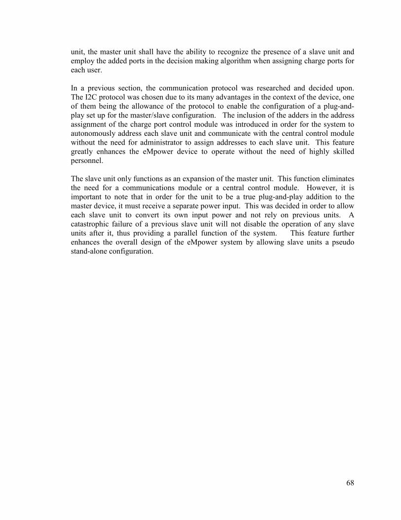
68
unit, the master unit shall have the ability to recognize the presence of a slave unit and employ the added ports in the decision making algorithm when assigning charge ports for each user. In a previous section, the communication protocol was researched and decided upon. The I2C protocol was chosen due to its many advantages in the context of the device, one of them being the allowance of the protocol to enable the configuration of a plug-and-play set up for the master/slave configuration. The inclusion of the adders in the address assignment of the charge port control module was introduced in order for the system to autonomously address each slave unit and communicate with the central control module without the need for administrator to assign addresses to each slave unit. This feature greatly enhances the eMpower device to operate without the need of highly skilled personnel. The slave unit only functions as an expansion of the master unit. This function eliminates the need for a communications module or a central control module. However, it is important to note that in order for the unit to be a true plug-and-play addition to the master device, it must receive a separate power input. This was decided in order to allow each slave unit to convert its own input power and not rely on previous units. A catastrophic failure of a previous slave unit will not disable the operation of any slave units after it, thus providing a parallel function of the system. This feature further enhances the overall design of the eMpower system by allowing slave units a pseudo stand-alone configuration.

69
Figure 48 Slave Unit Block Diagram
The slave unit need only contain a power regulation module and a charge port module. The elimination of unnecessary modules also decreases the cost of the slave unit, which is in keeping with the necessity of Water Missions to keep the units at a minimum cost. Each slave unit also retains the capability of an ON/OFF feature, as well as indicator LED’s for each port to inform the users when a port has been enabled (green LED) or disabled (red LED).

70
4.2 Software Design
The software design was approached using a top down method. This includes the view
from the device level to the client down to the actual action events of the software acting
upon the device. The Workflow was first explored to discuss the events that lead up to
the interactions of the client and the response of the unit. This clearly shows the events as
the client interfaces with the device and the feedback of the device from the keypad to the
LCD screen.
The Interface State Diagram was explored next to show the events from a state view of
the software acting upon the device. This shows the states that the device will be in as
events are initiated by the client as they interact with the keyboard in response to the
devices menu items.
4.2.1 User Interaction Workflow
The following Action and Response Sketch simulates the actions of the client and the charging devices interface. It demonstrates the activities of the client as they set up an account and how they will interact with the interface on the charging device to charge their phone.
The client will pay for the time he will use in blocks of a minute to the water missions team by whatever means are provided by Water Missions. This will be the sole responsibility of Water Missions and not the development team.
The server is set up with a new account or minutes are added to an existing account at the server level with Water Missions. A sample account on the server can be seen in the figure below. You can note that each solar charging device has its own unique ID number that will not be changed.

71
Figure 49 Sample Client Account
The charging device will communicate with the server every ten minutes to save in the overhead of the GSM communication fees. In the ten minutes the charging unit will do the following only on the client’s accounts that are inactive.
• Add new accounts to the charging device
• Update the existing accounts on the device
The client will enter their account number which is their phone number with area code and country code at the keypad where it will display the account number on the screen as they type it. This screen can be seen in Figure 48 below. If they need to change anything they can press the back key on the keypad in order to correct any mistakes. If they enter the wrong account number the device will repeat the entry screen again. The device will just loop until they enter the correct account number. They will then receive a message on the LCD that will ask for their pin number as seen in Figure 49 below. The pin was assigned to them when they paid for their minutes at the first step. They again will have the option of using the backspace to correct any mistakes that they make when entering their pin number. If they enter the incorrect pin number they will be given a total number of three tries before the device will go back to the entry screen for the entry of their account number again. When the client enters the correct pin number and presses the enter key a menu will appear as you can see in Figure 49 below.

72
Figure 50 Initial menu for phone number
Figure 51 Initial menu for pin number
The first choice will be “A: Start Charging”, if this option is chosen by the client the device will bring up another menu to determine if the client needs a USB or Cigarette Port as seen in the figure below. When the client chooses one the device will first check to see if a port is open for charging then assign a port. The port number will be assigned to the client and its light will turn on red indicating that the port is ready for use. If the client plugs their device into the port within 30 seconds the light will turn green indicating that the client is charging. If there aren’t any ports open then the LCD will display a message letting the client know that there are not any available ports and reset its self to the enter account number screen and not charge anything to the client. The client will be taken back to the main screen after charging has begun.

73
Figure 52 Main Menu setting up port
If the client unplugs their phone before their minutes are up then the device will stop charging their device. The light next to the port they are using will turn off and the LCD will show how many minutes they were charged for and how many minutes that is left on the account.
If the client is charging and they only have one minute left on their account then the light will turn red and begin flashing until the client either unplugs, where the device will respond as stated previously. If they wait until all their minutes are used up the light will turn off and stop charging their phone. In addition the display will show how many minutes they used and how many they have left on their account.
The second choice will be “B: See minutes remaining on your account”. If this option is chosen then the minutes will be displayed as seen in Figure 51where it will show the total minutes the client used in this session, total minutes the client has ever used, and how many more minutes are left on the account. The client will be taken back to the main screen after the minutes have been displayed for 5 seconds.

74
Figure 53 Main Menu checking minutes
The third choice will be “C: Exit my account” as seen in the figure below. If this option is chosen the clients will exit their account and the screen will loop to the first screen asking for their account number. If they are charging the device will continue to charge their device.

75
Figure 54 Main Menu choosing to exit
4.2.2 Interface State Diagram
The following in Figures 53 and 54 below are the state diagrams of the device during the Interfacing of its subsystems. This diagram will show the state of the unit from the server side and the device side.

76
Figure 55 Device side state diagram

77
Figure 56 Client side state diagram
4.2.3 GSM/GPRS Communications
Software Workflow
GSM/GPRS devices are controlled through a series of Attention (AT) Commands. These Attention Commands tell the GSM/GPRS module to do things such as send a text message, for example. Water Missions International has a certain set of criteria they would like us to meet in a custom command workflow for the device. These commands are specified as follows:
• Command to turn all charging ports on or off
• Command to send a custom text message (for entering the code to add
credit to prepaid SIM card in the eMpower box)
• Command to query the cumulative energy used with date time stamp
on the eMpower unit
• Command to update the interval (in minutes) how often the cumulative
energy used is logged into memory
• Command to query the date and time
• Command to update the date and time

78
• Command(s) to update where the SMS sends to (up to 4 different
phone numbers) or GPRS connects to (APN settings, domain,
protocol, etc)
• Command to update the reporting frequency of cumulative kWh
(daily, weekly or monthly)
• Command to update the eMpower unit’s ID number
• Each command will have a success or failure reply message.
• Each command will need a correct password entered before the
command is run. This password will precede the command and be in
the same SMS. There will be a different password for querying data
and configuring the unit. Unrecognized SMS will be ignored.
• Command to update the passwords
• Command to query all the settings on the eMpower unit
The first thing to address is how the device will be controlled remotely from an off-site administrator. Due to the GPRS side of the module having a dynamical IP address, there is no easy way to send data to the GSM/GPRS module. Data will be sent back to one of Water Mission Internationals MySQL servers through a TCP stack over the GPRS side of the network.
4.2.3.1 Remote SMS Receiving
The logical place to start, is how the device would receive commands by SMS from an off-site administrator. One of Water Missions International’s project specifications was that a password precedes every SMS command in order for security purposes. There will be a twofold security system. The first would be to parse the password from the SMS module and comparing it to the stored value within the SD card. If it passes this test it will then have the option of authorizing the senders telephone number by referencing the on board SIM card’s phone book to see if that telephone number is stored in it. If this authorization is successful then the microcontroller will continue on the parse the text within the SMS following the password and deciding what command to do. This secondary level of security will be optional; administrators will be able to decide whether or not they want it. If either one of these tests fail the program will continue to loop while waiting for new, unread text messages. You can see this first part of the program in the figure below.
79
Figure 57 Initial SMS Receiving Workflow
4.2.3.2 Command Execution Confirmation
All commands send to the device will give the sender feedback as to whether the device successfully executed the command. Feedback will include a string consisting of either “Command Success” or “Command Failure”. Additionally an option may be added to give a specific error code to so that the sending administrator can reference it to determine why the command was not executed. Reference codes will be stored in the SD card. An outline of this process can be seen below in the figure below.

80
Figure 58 Command Execution Confirmation Flow Chart
4.2.3.3 Command Execution Testing
The testing as to whether or not a command has been successfully executed can be taken into a more micro view. The process of executing the SMS can have several outcomes. Commands can be broken down into several broad categories. They can request data to the remote administrator, change data or add new data to the device’s SD card. Storage system Information that will be stored in the SD card memory will include the active user accounts information, such as their specific phone number, ID number and balance in minute intervals. Administrative passwords, device error codes, device logs and device parameters will also be stored on the SD card. At this point the SMS has now been

81
authorized to execute a command. The command execution testing phase can be seen in the figure below.
Figure 59 Command Execution Testing Flow Chart
The code to do all this will have certain checkpoints where specific segments of code check to make sure a function has been executed properly. If not it will debug to try to find the potential error and then reference the error to a specific error code within the library. However, if an error occurs with library communication and the microcontroller is unable to pull an error code from the SD card module, then it will either pull an error code from the microcontroller flash memory or EEPROM to reference an error code that library communication is currently not working.
4.2.4 Software Design Summary of
Communications Board
The software that will be used on the communications board will consists of some standard C, C++ and Arduino libraries that will be modified for our specific use. Fortunately Arduino has many libraries that will help in coding this project. It should be noted that the use of Arduino or any other libraries will take up space in the flash memory of the microcontroller. This in turn could limit the amount of code that can be used in the programming of your device and in turn limit the choices of microcontrollers to use on the device.

82
4.2.5 GSM Shield Library
The Arduino GSMSHIELD library contains a number of useful functions as a layer of abstraction that requires less code from the user to obtain the same results. Normally to do something such as send an SMS through the GSM module it would be necessary to write to it over serial the AT Command with the necessary parameters, followed by the text and then finally write an ending character to let the GSM module know that the command has been finished. When send an AT Command to read an SMS, for example, the SIMCOM900 returns a number of values such as the position of the text in the SIM cards memory, the sender’s phone number and the text within the SMS. This specific library was developed to support Open Electronic GSM/GPRS Shield board, but will be modified to work with our Seeed Studio board. It already has been modified and verified that this will indeed work with the Seeed Studio board.
This provides that the user write a lot of code to complete something as simple as reading and parsing text from an unread text message. Fortunately this library takes care of all of this. This library takes care of basic functions such as reading an SMS, checking for unread or read SMS’s stored within the SIM’s memory and a number of other features. Just a few functions included in this library can be seen in Table 11 below.
Table 10 Table of some of the available SMS functions of the GSMSHIELD library

83
Reprinted from www.open-elecontrics.org, permission pending
Of course this library only takes care of most of the basic functions of the SIMCOM900 so it will be modified to include custom functions that will accommodate the necessary design requirements. It also includes some useful functions that will be used for our GPRS communications with the server. Some of these functions can be seen below in Table 12.
Table 11 Table of some of the available GPRS functions of the GSMSHIELD library
84
Reprinted from www.open-electronics.org, permission pending
4.2.6 Keypad Library
Arduino has a great little library for using matrix based keypad implementations that will fit perfect for this project. This library lets you map out your keypad in a matrix fashion by row and column. It includes the following functions that will be utilized for the implementation of the keypad in to this project.
• void begin(makeKeymap(userKeymap)) o Initializes the internal keymap to be equal to userKeymap
• char waitForKey() o This function will wait forever until someone presses a key. Warning: It
blocks all other code until a key is pressed. That means no blinking LED's, no LCD screen updates, with the exception of interrupt routines.
• char getKey() o Returns the key that is pressed, if any. This function is non-blocking.
• KeyState getState() o Returns the current state of any of the keys.
The four states are IDLE, PRESSED, RELEASED and HOLD.
• boolean keyStateChanged() o New in version 2.0: Let's you know when the key has changed from one
state to another. For example, instead of just testing for a valid key you can test for when a key was pressed.
• setHoldTime(unsigned int time) o Set the amount of milliseconds the user will have to hold a button until the
HOLD state is triggered.

85
• setDebounceTime(unsigned int time) o Set the amount of milliseconds the keypad will wait until it accepts a new
keypress/keyEvent. This is the "time delay" debounce method.
• addEventListener(keypadEvent) o Trigger an event if the keypad is used.
4.2.7 SD Card Library
The Arduino SD card library provides a number of useful functions that will be used in this project. Although these functions are for the most part basic, such as finding if a director exists, removing a directory, and opening a file, just to name a few, it will be modified for our specific purposes. Modifications will include functions to search for strings of certain parameters stored within .txt files, search for specific strings within .txt files, and finally adding strings and removing string from the .txt files.
5. Parts Acquisition
The Acquisition of parts will be done mostly by use of the internet electronic sales sites. The sites that we have explored thus far include Newark, Avnet Express, Mouser, Digi-key and Octopart. It was found that Newark and Digi-key had the highest prices but they also had a lot of deals on free shipping. Digi-key seemed to maintain the most stock of items and Mouser and Avnet Express had the lowest prices. The approach to ordering online will depend on not only the price but the availability. If the product is needed now then looking at a distributer that offers fast delivery and who has the product in stock may be the way to go. If we aren’t in any rush then we may just go with the cheapest approach as long as they are in stock or can get the product in a reasonable amount of time. It is worth mentioning that some of the items needed can be purchased through local dealers such as Skycraft and Radio Shack. In fact, it was a surprise that Radio Shack actually carried one of the GSM modules that we were considering. This would be a real advantage if time was of the essence. In conclusion it is impossible to say which method will be used in the acquisition of parts due to its dependency on how soon we need the part or how much we can spend on it.

86
5.1 Parts List
eMpower Master Unit Parts List Item Reference
Designator
Description Part Number Manufacturer Quantity
1 PS Power supply Module EMP-001 Water Missions 1
2 CPC Change port control
Module
EMP-002 Water Missions 1
3 CC Communication control
Module
EMP-003 Water Missions 1
4 CEC Central control Module EMP-004 Water Missions 1
5 KP 4x4 Keypad 96BB2-006-F Grayhill 1
6 LCD 4 x 20 LCD screen LCM2004SD-NSW-BBW Grayhill 1
7 SW1 SPST ON/OFF Rocker
Switch
PRCSA1-20L-BB0CW TE Connectivity 1
8 -- Housing EMP-005 Earnest Products 1
Table 12 Master Unit Parts List
EMpower Slave Unit Parts List
Item Reference
Designator
Description Part Number Manufacturer Quantity
1 PS Power supply Module EMP-001 Water Missions 1
2 CPC Change port control
Module
EMP-002 Water Missions 1
3 -- Housing EMP-006 Earnest Products 1
Table 13 Slave Unit Parts List

87
5.2 BOMs
Communication Control BOM Item Reference
Designator
Description Part Number Manufacturer Quantity
1 -- GPRS Shield SLD33149P Seeed 1
2 -- GSM Module GE865 Tellit 1
Table 145 Communication Control BOM
Central Control BOM Item Reference
Designator
Description Part Number Manufacturer Quantity
1 U1 Microcontroller mega2560 ATMEGA2560-16AU 1
2 U2 Microcontroller mega8 ATMEGA8U2-MU 1
3 D1 LED(YELLOW) HSMG-C170 1
4 D2 LED(GREEN) HSMG-C190 1
5 D3 LED(RED) HSMG-C150 2
6 R1 Resistors 10K CAY16-103J4LF 8
7 R2 Resistors 1K CAY16-102J4LF 8
8 R3 Resistor 1M CR0603-FX-1004ELF 2
9 C1 Capacitor 22pf C0603C220J5GACTU 5
10 C2 Capacitor 100nf TYC0603B104KDT 11
14 C3 Capacitor 1uf C0603ZRY5V6BB105 1
15 SW1 Reset Button B3F-1000 1

88
16 RES 16MHZ Resonator FOXSLF/160-20 2
17 P1 Pinheader 1x8 825433-8 4
18 P2 Pinheader 1x5 825433-5 2
Table 156 Central Control BOM
Charge Port Control BOM Item Reference
Designator
Description Part Number Manufacturer Quantity
1 PCB PC Board, 35 sqin, 2 layer TBD TBD 1
2 MCU2 AVR Microcontroller, 16KB ROM ATMega 169A Atmel 1
3 R1,3,6-12 220 Ohm resistors Standard - 8
4 R2,4 1k Ohm Resistor Standard - 2
5 R13 10k Ohm resistor Standard - 1
6 C1,2 10 uF capacitors Standard - 2
7 RES1 16 MHz clock crystal 774-ATS16B CTS 2
8 C3,4 22 pF capacitors Standard - 4
9 I1 60 ohm @20Mhz BEAD MPZ1608S101A TDK 1
10 PB1 Reset tac button 506-FSM6JH Alcoswitch 1
14 IC1-10 USB charging port controller TPS2511 Texas Instruments 10
15 IC11-12 USB Plugs 931 Keystone 10
16 P11,12 Socket Cigerette Screw lock plug ZA2060 MDP 2
17 IC13 4 bit full adder DIP 74HC283N,652 NXP Semiconductor 1
18 FU1,2 PCB blade fuse holder 01000057Z Littelfuse 4
19 LED1-
12,25,26
Green LED LTL-307G Lite-On 14

89
20 LED13-24 Red LED LTL-307E Lite-On 12
21 MT1-26 LED Holders CB55 Kingbright 26
22 - 20 g wire, Red (feet) 4
23 - 20 g wire, Black(feet) 4
Table 167 Charge Port Control BOM

90
6. Project Prototype Testing
In order to ensure that all specifications provided by Water Missions were met, several testing protocols were created. Each protocol described is comprised of several sections.
• Protocol number – This assigns a number to each testing protocol for easy tracking
• Objective – describes the purpose of the testing protocol
• Goals – Describes the given specifications given
• Test Equipment – Describes the necessary test equipment to complete the procedure
• Procedure – Describes the steps to be taken in order to prove the desired outcome
• Documentation – provides a template to document the testing results
For both the hardware and software testing protocols this same template will be used, in order to provide a well-documented testing procedure that can then be surrendered to Water Missions.
6.1 Hardware Specific Testing
The primary objective of hardware testing is to provide the developers with a well-documented procedure to ensure that the device is in compliance with the given specifications. These procedures include the following:
• Communication and data saving devices continue to operate with a secondary
supply voltage of 12 VDC (#H01)
• Secondary power supply disengages upon detection of a primary supply voltage
(#H03)
• Slave unit is recognized by the master unit (#H04)
• Each USB and car lighter socket port function as specified (#H05)
Though the given specifications from Water Missions specify a storage and operating
temperature range, the current scope of the hardware testing will not include
environmental testing. The decision to exclude environmental testing was made upon
conclusion that the cost of such testing would exceed the budget for this project. All test
data will be provided to Water Missions upon completion of the development of the
device.

91
6.2 Software Specific Testing
The primary purpose of this section is to ensure that the software developed meet or exceeds the required specifications of Water Missions. Furthermore, a few other protocols were developed to ensure that the interconnectivity between all devices that communicate with the central control module is operational. The following protocols were developed for this purpose.
• Ensure required SMS commands are executed within the device (#S01)
While the testing protocols serve as a way to document that the device meets the requested specifications they are not the only testing that will be conducted by the developers in order to meet and exceed the given criteria by Water Missions. While in the development stage, the software will be tested in three phases. The first phase will be performed on a development board. These boards will be used to determine that the components that we plan to use will work for the project specifications as noted in Water Missions specifications. Each component will be tested with the development board, then when all tests have been completed all the components of that block will be connected and testing will be performed on those components working in succession of each other. When the components are connected individually an interface will be necessary to see the results from the testing. This interface will be the Arduino open-source environment. The second phase of testing will be done on a prototype mockup of a board of our own design that is based off of the development board used in the previous testing phase. This board will then be tested in the same manner where each component will be tested separately then together as a unit. The last phase consists of using the finished PCB (printed circuit board) and will entail the use all the components since they will all be attached to the board at once.
6.2.1 Phase One – With development board
6.2.1.1 Keypad Only
The first set of tests will use the Arduino uno in conjuction with the open-source Arduino environment with the keypad:

92
• Step No: 1
Step Description: Plug in the Arduino to the computer and make sure the Arduino environment running on the PC has a connection with the Uno board by sending a command to turn the on board LED.
Expected Results: When the sketch is uploaded the LED should turn on
• Step No: 2
Step Description: Connect the keypad to the Arduino Uno and press the keys on the keypad from the upper top left corner by column and then by row until all the buttons have been pressed once.
Expected Results: The output of the Arduino interface should coincide with the keypad as shown in the figure below.
1
4
7
back
2
5
8
0
3
6
9
A
enter
B
C
D
Figure 60 Keypad configuration
• Step No: 3
Step Description: A key on the key pad will be held down for 5 seconds and then released.
Expected Results: The output on the Arduino interface should only show one output of the key that was depressed.
• Step No: 4
Step Description: A key on the keypad will be held down then a second key will be pressed while the first is still being held down. Both keys will then be released.

93
Expected Results: The first key depressed should be the only number displayed on the Arduino interface.
• Step No: 5
Step Description: A key will be depressed repeatedly as fast as the user can depress the key of a single key.
Expected Results: The key should be repeated as fast as the key is depressed showing a one for one feedback on the Arduino interface.
• Step No: 6
Step Description: Many keys will be depressed on a one by one bases as fast as can be done.
Expected Results: All the keys that were depressed should show up on the Arduino interface.
6.2.1.2 LCD Only
• Step No: 1
Step Description: Plug in the Arduino to the computer and make sure the Arduino environment running on the PC has a connection with the Uno board by sending a command to turn the on board LED. Expected Results: When the sketch is uploaded the LED should turn on
• Step No: 2
Step Description: Plug the LCD into the board set the backlight to its brightest and send a printout to the LCD screen.
Expected Results: The printout should be readable in low to high lights environments.
• Step No: 3
Step Description: Print four lines of code to the LCD that should display on four different lines of the screen.
Expected Results: The four lines should be displayed on the LCD where each has its own line and they are in the order they were sent as can be seen in figure 7.4.1.2a below.

94
Figure 61 Output on LCD with four lines
6.2.1.3 GSM/GPRS Module Only
• Step No: 1
Step Description: Connect the Module to the development board and make a connection to the cell provider.
Expected Results: The output should be that the module is connected and send back a ready signal
• Step No: 2
Step Description: Send a text from the module to an telephone and send a text from a telephone to the module.
Expected Results: The module should receive the text and display its contents on the interface screen and when sending a text it should be received by the telephone and display the correct characters.
6.2.1.4 Keypad/LCD/GSM Together
At this point all the components have been tested individually. They will now be tested to make sure that there software will work together on the development board.
• Step No: 1
Step Description: The unit will be powered up.

95
Expected Results: The LCD will display a welcome screen that includes the current date and time as seen in the figure below.
Figure 62 LCD Splash Screen
• Step No: 2
Step Description: On the menu screen a valid account number will be entered using the keypad followed by the enter key.
Expected Results: The LCD will ask for the pin number to the account.
• Step No: 3
Step Description: A valid pin number will be entered on the keypad followed by the enter key.
Expected Results: The main menu will come up displaying options “A: Start Charging”, “B: See minutes remaining on account”, and “C:Exit”
• Step No: 4
Step Description: An “A” will be entered at the main menu for “Start Charging”, using the keypad followed by the enter key.
Expected Results: The LCD will respond with the question on if you need a USB or Cigarette port.
• Step No: 5
Step Description: An “A” or “B” will be entered on the keypad followed by enter on the main menu.
Expected Results: The LCD will show the choice followed by the port number that is assigned. That port will then be active for charging
• Step No: 6
Step Description: A “B” is entered at the main menu for “See min…..”, followed by the enter key.
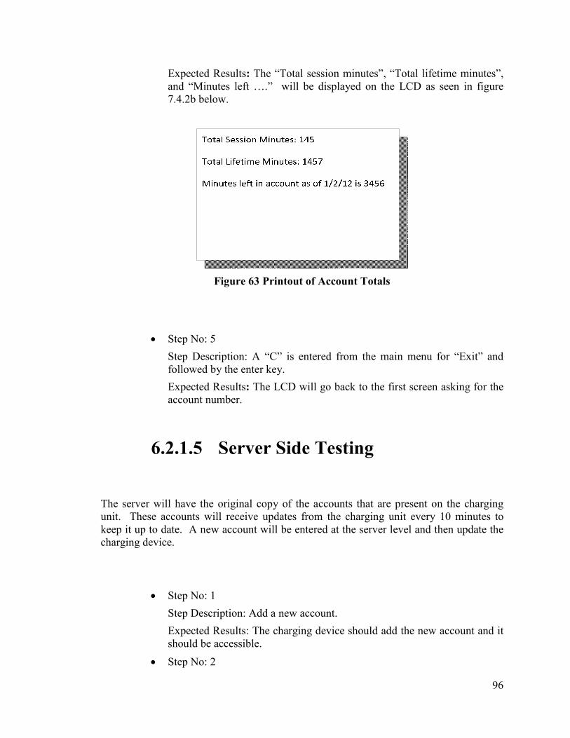
96
Expected Results: The “Total session minutes”, “Total lifetime minutes”, and “Minutes left ….” will be displayed on the LCD as seen in figure 7.4.2b below.
Figure 63 Printout of Account Totals
• Step No: 5
Step Description: A “C” is entered from the main menu for “Exit” and followed by the enter key.
Expected Results: The LCD will go back to the first screen asking for the account number.
6.2.1.5 Server Side Testing
The server will have the original copy of the accounts that are present on the charging unit. These accounts will receive updates from the charging unit every 10 minutes to keep it up to date. A new account will be entered at the server level and then update the charging device.
• Step No: 1
Step Description: Add a new account.
Expected Results: The charging device should add the new account and it should be accessible.
• Step No: 2

97
Step Description: Add minutes to an existing account.
Expected Results: The account on the charging device should be updated with the new amount of minutes.
• Step No: 3
Step Description: Delete a account.
Expected Results: The corresponding account on the charging device should be deleted.
• Step No: 4
Step Description: Add more than one account
Expected Results: There should be more then one account
6.2.1.6 SD Card Storage Testing
• Step No: 1
Step Description: Send SD Card new information
Expected Results: New information should be stored within the SD card
• Step No: 2
Step Description: Pull Information from SD card
Expected Results: Information will be pulled from the SD card to the microcontroller
6.3 Testing Protocols
The following section contains all testing protocols developed for this device. The testing protocols serve as a verification tool to provide to Water Missions a way to ensure that the devices meets and exceeds specifications. This documentation will be turned over to Water Missions upon completion of the device.
Protocol # H01
Port Testing Protocol

98
Turn on Delay and Rise Time with 22-uF Load:
The purpose of this is to verify that there are no detrimental voltage spikes or EMF noise created when a device is plugged in or unplugged:
Turn on delay rise time – Actual measured 2.48ms
Turn on delay rise time – Per datasheet: 3.0ms

99
Turn off Delay and Fall Time with 22-uF Load:
Turn off delay fall time – Actual measured 46.8ms
Turn off delay fall time – Per datasheet: 2.0ms

100
Handshaking between TPS 2511 USB Controller and mobile device (DCP Auto-
detect):
This is a the BC1.2 DCP handshaking auto-detect. It should be included in the section describing eather the handshaking or the testing.
DM (data 0) – Yellow DP (data 1) – Blue
Step 1) 2.4v on DM, 2.6v on DP at t= 0ms, to stimulate handshaking feature in mobile
device.
Step 2) 3.0v impulse on both DM and DP at t = 100ms from mobile device, to
acknowledge proper handshake received.

101
Step 3) 2.7 on both DM and DP to begin charging at t = 200ms, to provide charging to
the BC1.2 compliment device.
Protocol # S01
SMS Command Testing Protocol
All necessary safety precautions must be observed when performing all testing protocols. Special care should be taken when using the device in voltages higher than 60 VDC.
Objective:
Ensure that each SMS command executes as required
Goals:
• Send each SMS command to the device.
• Confirm receipt and execution of desired action
• Send SMS commands to the server
• Confirm receipt and execution of desired action
Test Equipment:
• SMS Device
Procedure:
1. Ensure proper connection of all modules.
2. Provide the Master unit primary input with a DC Voltage of 30 VDC.
3. Send SMS commands to the device and verify desired action is executed.
4. Record results in the documentation section of this testing protocol.

102
5. Repeat for each SMS command in the section
6. Disconnect all power from the master unit
Documentation:
SMS Command Name Action Pass/ Fail
a ALL PORTS ON Command to turn all ports on Pass
b ADD CREDIT Command to initialize add credit routine Pass
c CREDIT Command to query available credit Pass
d ENERGY Command to query energy used Pass
e ENERGY INTERVAL Command to update interval time Pass
f DATE TIME Command to query date and time Pass
g CHANGE DATE TIME Command to change date and time Pass
h UPDATE SMS Command to change where the SMS sends
Pass
i UPDATE ID Command to update eMpowers unit ID Pass
j SETTINGS Command to query all settings Pass
7. Administrative Content
The following is a copulation of the milestones that the team will meet as the project moves forward in a week by week progression. It will in turn consist of a budget and financial discussion of how much was budgeted for the project and what actions are to be taken due to different scenarios of monetary support. In Addition, the goal of the project is to turn the device over to Water Missions , but this must be done in a professional and organized manner.
7.1 Turnover to Water Missions
The project will be in an advanced prototype phase when turned over to the Water Missions Group. This means that although the project is a prototype it will have some of the qualities of a finished ready for field model. The field model portion will include all

103
the input and output voltage ranges as specified, all the charging ports including and not limited to 10 USB and 2 cigarette lighter socket ports, all of which will be fashioned with resettable fuses and LED’s indicator lights. The housing will be made from a punched out aluminum body that will be to exact specifications, to promote reuse in the finalization of the field model and to stay consistent with Water Missions goals of recyclability. There will be a second satellite housing that will have the same qualities stated previously in the main housing. It will be an extension to the main housing for additional charging ports. The LCD and Keypad will meet with the expectations of the temperature highs and lows in Africa and other tropical environments, but will not be water resistant and cannot be exposed to direct contact with the elements and precipitation. This limitation is why the device is considered advanced prototype phase as opposed to field ready. In addition the coding of the device will allow for the updating and usage of accounts on the device. It will connect with a land based server that will be used to send updates to the device for field usage. The client will have the ability to access a newly created account or an existing one by use of the keypad and login using a password to charge their device on one of the ports provided. The software will turn on the charging port when a device is plugged in and cease charging once that device is unplugged. In turn, the device will update itself as the clients minutes expire, therefore alerting the LED’s on the device to respond accordingly. The code will only allow for the client to charge when they have minutes and will update the land based server after the client unplugs their charging devices. The device will meet or exceed all specifications as noted in 2.4.1 Water Missions specifications
The orders of events leading up to the turnover of the device are as follows:
• Completion of documentation to Water Missions
• Testing of the device
• Communication to Water Missions on Status
• Training to Water Missions of Functions and operation of the device
• Signing over of ownership to Water Missions
• Follow up
The documentation will include all the code to the project so it can be expanded upon for future deployment of the device. The engineers will be educated on how the device generally works with the code and how to manipulate the code to change parameters for such things as updating of the server, port recognition or whatever else they may need to change to fit their needs. The code will include a good deal of documentation to assist in the education of the Water Missions engineers understanding of the code. The documentation will also include a user manual for the operation of the device and troubleshooting techniques.

104
The device will be tested before the turn over for a final testing to make sure that there was no damage done to the device in the final hours of its completion. It will be tested using our testing procedures that are laid out within this documentation. If there are any problems, there will be field repairs attempted and if that is unsuccessful then the turnover will be delayed until such repairs can be made.
When the device is tested and has passed the entire test for a final time, the device will be ready for turnover and therefore Water Mission will be contacted to set up a meeting for the next phase of training to their staff. The meeting will consist of all the completion team and split into two categories. One team will handle the implementation of the hardware and the other will involve the implementation of the software. The meeting will be set up in a place convenient to both parties and will follow a series of events as noted in the following procedures.
The staff will be trained in the operation of the device including setting up accounts, polling the System, account management, and device troubleshooting. They will be given the training manual and monitored to determine if they can set up the device for deployment and operate the device using the manual exclusively. If there are any discrepancies with the manual these discrepancies will be corrected and the staff will be re-tested until the staff is confident that the device can be deployed in the field and others be trained using the manual and operated to produce the required results.
When the staff is adequately trained on the device it will be turned over to them for further testing and upgrades by their core of engineers. They will have full ownership of the device at this time and will be able to add any functions that are needed to support their mission or alter any of the hardware or software to meet the Water Missions goals and objectives. They will then be able to use this prototype to create a field worthy device that will be able to be recreated or cloned to meet present and future needs of deployment of such devices to other Water Missions projects.
Follow up will be provided to help support Water Missions goals. The completion team will provide any help with hardware knowledge for further implementation and with the discretion of the team member they will stay involved as much as they deem necessary to enhance the abilities of Water Missions engineers. The team will provide software as well as hardware support to the device through email and phone, and if needed the team member can choose to provide their personal services to help Water Missions in the further development of the device or deployment of said device.

105
7.2 Budget and Finance Discussion
The budget can be seen in Figure 62. It consisted of the budget of the project organized by the sub categories of the different module blocks followed by any other contributing budget expenses. This is then followed by other contributing budget expenses. The budget sheet includes the cost and estimated shipping if it applies to the line item. At the end each category is subtotaled and a cushion of 5 percent is added and a final total is added the end. The budget will be presented to Progress Energy for evaluation and possible funding. If they do not fund the project or only partially fund the project, then Water Missions will be approached to fund all or part of the project. If the project is still not funded completely then the decision would have to be made to either split up the project expenses equally to the team members or go back and try to finish the project more inexpensively. This could be accomplished by ordering on price only and not be as concerned on the turnaround time or order other brands of the more expensive items to save money. An alternative could also be to look for other funding from nonprofits that may work with Water Missions or an outside nonprofit that has interests in third world charity.
7.2.1 Budget Sheet Breakdown
It was determined to be easier to follow the layout in this manner due to the organization of the document by the different blocks that are to be created in senior design 2. It was found that there are a lot of underlying expenses to building a project and these are included in at the end to give a holistic compilation of the costs that will be incurred by the end of the project. Most of the items on the sheet have the correct cost of the items to be ordered and the site we got the cost from. A section to include the tax and shipping was added due to the high shipping cost of many of the items. This was found to increase the budget by a reasonable amount so was included with its own column. Each sub category was subtotaled with a final total to illuminate the expense for each subcategory for further evaluation in the case of possible cutbacks due to a lack of funding. The funding will not be known until possibly the beginning of the Spring 2013 so it was determined that this format would streamline any possible cuts or further bargain shopping due to budget needs. It was determined that every possible expense would not be accounted for so a risk cushion of 5 percent was added to cover any unforeseen expense that may be incurred. This would also include the possibility any accidents with the modules that would necessitate there replacement reconstruction.

106
Sub Category Task Description CostTax &
ShipTotal
Surge Protection fusable l ink, mouser.com $10.00 $2.00 $12.00
DC/DC converter lpa series eico electonics $200.00 $7.00 $207.00
Circuit board(PCB) www.pcb.net up to 4 layers, up to 60 square in $50.00 $5.00 $55.00
Subtotal 1 $260.00 $14.00 $274.00
Power interruptor Digital I/o IC, 12 *1.50, mouser.com $18.00 $2.00 $20.00
Power Regulator Voltage Regulator IC 25 * .50, mouser.com $12.50 $2.00 $14.50
Curr/Volt Monitor Analog to Digital convertor IC's , mouser.com $50.00 $2.00 $52.00
Interface Plugs 12 * usb, 2 * Cigarette, mouser.com $20.00 $2.00 $22.00
Misc. Elect. Comp. mouser.com, resistors, capacitors, etc.. $30.00 $3.00 $33.00
Circuit board(PCB) www.pcb.net up to 4 layers, up to 60 square in $50.00 $5.00 $55.00
Subtotal 2 $180.50 $16.00 $196.50
Circuit board(PCB) www.pcb.net up to 4 layers, up to 60 square in $50.00 $5.00 $55.00
AssT components usb. Barrel jack, resister, cap,crystal $40.00 $2.00 $42.00
Microcontroller AT Mega 2650 $16.00 $3.00 $19.00
Subtotal 3 $106.00 $10.00 $116.00
GSM Module Telit www.newark.com part no. GE863GPS730 $136.85 $7.00 $143.85
simcard T-mobile $100.00 prepaid phone card dataplan $50.00 $0.00 $50.00
Antenna ADA-0062Q/U-SMA, gsm antenna,newark $15.11 $5.00 $20.11
Simcard slot newark 101-00306-82 - MEMORY SOCKET, SIM, 6POS $1.50 $0.00 $1.50
Circuit board(PCB) www.pcb.net up to 4 layers, up to 60 square in $50.00 $5.00 $55.00
Subtotal 4 $253.46 $17.00 $270.46
Shop time UCF Mecanical Engineering lab $20.00 $0.00 $20.00
Housing fab. Southern Manufacturing, longwood florida $50.00 $0.00 $50.00
Tools Soldering Iron, flux, Multimeter, varies clamps $50.00 $5.00 $55.00
Lcd screen store.nkcelectronics.com, 20x4 lcd, white backlight $25.00 $5.00 $30.00
Keypad digikey.com, 16 key black, mgr1549-nd $44.00 $1.00 $45.00
Bread board Ramsey WBU206 Breadboard 2390 tie points,amazon $30.00 $3.00 $33.00
Deep Cell Battery www.batteriesplus.com $60.00 $10.00 $70.00
BATT-BACK Chgr $15.00 $4.00 $19.00
Slave Unit Includes all comp. except Gsm module and batt $752.35 $37.00 789.35
Solar Panels 45 watt, harbourfreight.com $189.99 $15.00 $204.99
Subtotal 5 $1,236.34 $80.00 $1,316.34
$2,036.30 $137.00 $2,173.30
$108.67
$2,036.30 $137.00 $2,281.97
Other Contributing Budget Expenses
Subtotals
Risk Cushion(5%)
Total
Mobile Charging Device BudgetBudget by Project Block including Misc. Expenses
Input Power Regulation / Protection
Power and Charge Control
Central Control
Communication Control
Table 17 Mobile Charging Device Budget

I
Appendix A Image Permission Requests
1. Open-Electronics www.open-electronics.org is an archive of opensource electronic projects created by Elettronica In. Information featured on this website is available for everyone to use, including but not limited to reviewing and modifying the source code. This open source site allows for modification, redistribution and commercial use.
Figure 64 Open Electronics GSM Remote Control – 2 IN and 2 OUT Figure 65 SIMCom Sim900 Breakout Board from Open Electronics Figure 66 SIM900 Breakout Board from Open Electronics Figure 67 GSM/GPRS Shield Schematic from Open Electronics Figure 68 GSM/GPRS Shield from Open Electronics
2. Rocket Scream Permission was requested from www.rocketstream.com via email. A response was received and included here.
Figure 69 Rocket Scream’s TraLog Schematic

II
www.rocketscream.com Permission to use Images
3. GoCharge Permission was requested from www.gochargenow.com via email A response was received and included here.
Figure 70 GoCharge’s Themis Free standing charging kiosk
Response from www.gocharge.com

III
4. NV3 Technologies Permission was requested from www.nv3tech.com via email. As of the printing date of this document, a response has not been received.
Figure 71 NV3 Technologies’ NTC-1912 Cell phone charging kiosk Figure 72 Brightbox charging kiosk
www.nv3technologies.com Permission to use Images
5. Ken Shirriff’s blog Permission was requested from www.arcfn.com via email. As of the printing date of this document, a response has not been received.
Figure 73 Apple iphone Charger Schematic
6. Sparkfun In www.sparkfun.com/static/about graphics downloads section, the site authorizes the use of graphics and photos for “personal, non-commercial use” and for the use in “project documentation or reports”
Figure 74 Sparkfun GE865 Breakout Board Schematic
Figure 75 Sharp TFT-LCD Display

IV
Figure 76 Schematic of Main Communications Module
Figure 77 Mega2560 USB Interface
www.sparkfun.com Graphics Use Policy
7. Seeed Permission was requested from www.seeedsutido.com via email. As of the printing date of this document, a response has not been received.
Figure 78 Seeed Studio GPRS Shield Figure 79 Seeed Studio GPRS Shield Schematic
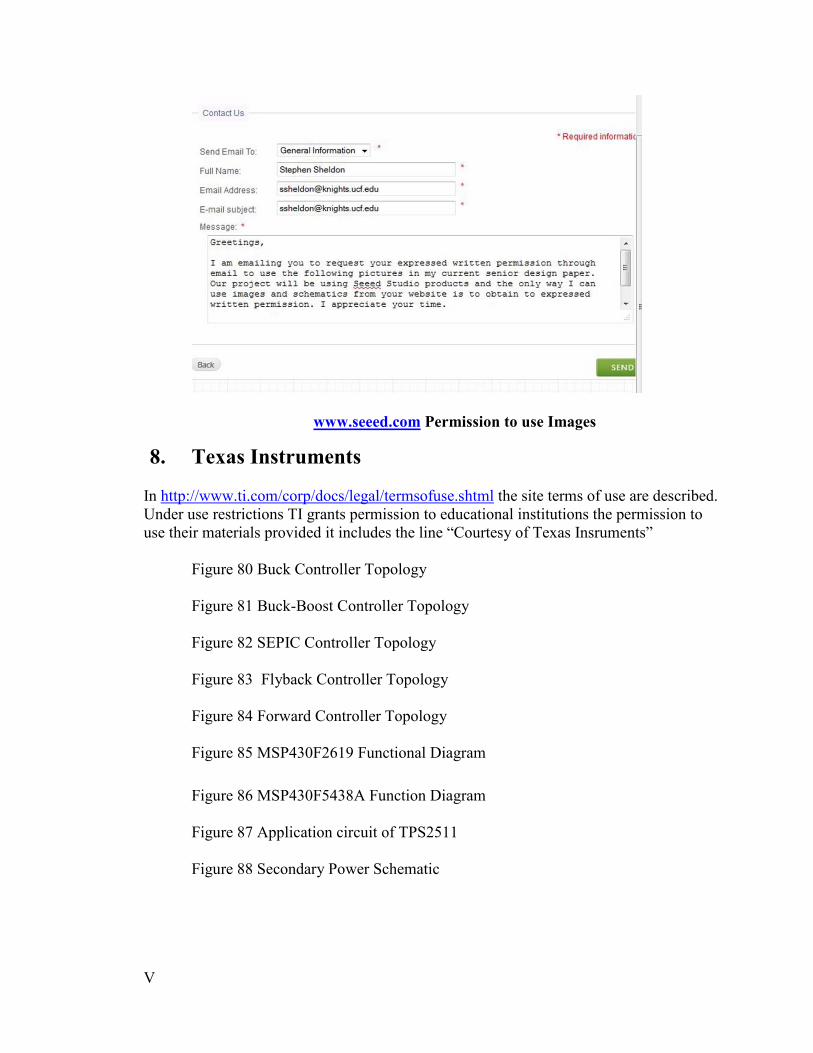
V
www.seeed.com Permission to use Images
8. Texas Instruments In http://www.ti.com/corp/docs/legal/termsofuse.shtml the site terms of use are described. Under use restrictions TI grants permission to educational institutions the permission to use their materials provided it includes the line “Courtesy of Texas Insruments”
Figure 80 Buck Controller Topology Figure 81 Buck-Boost Controller Topology Figure 82 SEPIC Controller Topology Figure 83 Flyback Controller Topology Figure 84 Forward Controller Topology Figure 85 MSP430F2619 Functional Diagram
Figure 86 MSP430F5438A Function Diagram Figure 87 Application circuit of TPS2511 Figure 88 Secondary Power Schematic
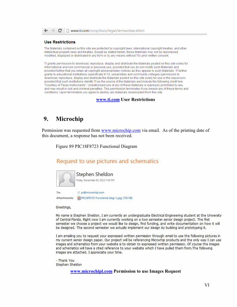
VI
www.ti.com User Restrictions
9. Microchip Permission was requested from www.microchip.com via email. As of the printing date of this document, a response has not been received.
Figure 89 PIC18F8723 Functional Diagram
www.microchipl.com Permission to use Images Request

VII
10. Parallax Permission was requested from www.parallax.com via email. As of the printing date of this document, a response has not been received.
Figure 90 Propeller P8X32A-Q44 Functional Diagram
www.parallax.com Permission to use Images Request
11. Atmel Permission was requested from www.atmel.com via email. . A response was received and included here.
Figure 91 ATmega328P-PU Functional Diagram Figure 92 ATmega2560-16AU Functional Diagram Figure 93 Pin Mapping of Arduino Mega

VIII
www.atmel.com permission to use images
12. Grayhill Permission was requested from www.grayhill.com via email. . As of the printing date of this document, a response has not been received.
Figure 94 Grayhill 4x4 Keypad Figure 95 Grayhill Series 86 4x4 Keypad Terminations and Truth Table

IX
www.grayhill.com Permission to use Images Request
13. Adafruit Permission was requested from www.adafruit.com via email. . A response was received and included here.
Figure 96 Adafruit microSD breakout board.

X
14. Poweresim Permission was requested from www.poweresim.com via email. . A response was received and included here.
Figure 97 Primary Power Supply First Stage Figure 98 Primary Power Second Stage Schematic

XI
www.poweresim.com Permission to use schematics
15. Group 32 Images In the case of the figures listed below, the members of group 32 snapped photos, created diagrams and or schematics. These images are original content and are printed here with the expressed consent of each group memeber
Figure 99 Apple Charging Unit Figure 100 GSM Network Structure Figure 101 Front view of charging unit showing location of LCD and keypad Figure 102 Grayhill 4x4 Keypad Layout Figure 103 LCM2004SD-NSW-BBW 20x4 LCD Figure 104 LCD Screen layout Figure 105 Pin layout Figure 106 Longtech Optics LCD Display Figure 107 I2C Addressing Circuit Figure 108 Master Unit Block Diagram Figure 109 Slave Unit Block Diagram Figure 110 Sample Client Account

XII
Figure 111 Initial menu for phone number Figure 112 Initial menu for pin number Figure 113 Main Menu setting up port Figure 114 Main Menu checking minutes Figure 115 Main Menu choosing to exit Figure 116 Device side state diagram Figure 117 Client side state diagram Figure 118 Initial SMS Receiving Workflow Figure 119 Command Execution Confirmation Flow Chart Figure 120 Command Execution Testing Flow Chart Figure 121 Keypad configuration Figure 122 Output on LCD with four lines Figure 123 LCD Splash Screen Figure 124 Printout of Account Totals

XIII
Appendix B Bibliography
“GSM Remote Control – 2 IN and 2 OUT Part 2 – Schematic” Open Electronics, January
2011 <http://www.open-electronics.org/gsm-remote-control-2-in-and-2-out-part-2-
schematic/>.
“GSM Remote Control – 2 in and 2 out”, Open Electronics Store, 2012 <http://store.open-electronics.org/Remote-control/GSM%20Remote%20Control/GSM%20Remote%20Control%20%E2%80%93%202%20IN%20and%202%20OUT>. GSM Remote Control – GSM Module, Open Electronics, January 2011 <http://www.open-electronics.org/gsm-remote-control-part-6-gsm-module/>. “Color 24-Bit LCD 4.3 PSP 480x272”, Sparkfun Electronics, 2011 <https://www.sparkfun.com/products/8335>. “PIC vs. AVR”, ladyada.net, April 2012 <http://www.ladyada.net/library/picvsavr.html>. “Using Microcontrollers(Atmel AVR and Microchip PIC”, Jumper One, October 12, 2011 <http://jumperone.com/2011/10/using-microcontrollers/>. “Memory Organization”, Romux.com, 2009 <http://www.romux.com/tutorials/pic-tutorial/memory-organization>. “Products”, Microchip, 2011 <http://www.microchip.com>. “8 bit Microcontrollers”, Mouser Electronics, 1996 <http://www.mouser.com/ProductDetail/Microchip-Technology/PIC18F8722-I-PT/?qs=sGAEpiMZZMtLck3p7ZBovTx1%2fOIQ%252baq2>. “TI MSP430”, Wikipedia, November 2012 <http://en.wikipedia.org/wiki/TI_MSP430>. “Texas Instruments MSP430F5438AIPZ”, Mouser Electronics, unknown <http://www.mouser.com/ProductDetail/Texas-Instruments/MSP430F5438AIPZ/?qs=sGAEpiMZZMu7K1a5XxETusGnaMgswLgC>. “MSP430F2619”, Texas Instruments, unknown <http://www.ti.com/product/msp430f2619>. “Atmel AVR”, Wikipedia, November 10, 2012 <http://en.wikipedia.org/wiki/Atmel_AVR>.

XIV
“Programmers”, Atmel, unknown <http://store.atmel.com/PartDetail.aspx?q=p:10500054>. “Parallax Propeller”, Wikipedia, October 7, 2012 <http://en.wikipedia.org/wiki/Parallax_Propeller>. “Using the AVR ISP mkii (USB) to burn the bootloader on MacOS”, Arduino Playground, unknown <http://arduino.cc/playground/Code/OSXISPMKII>. “ATmega bootloader programmer”, Gammon Software Solutions forum, May 2010 <http://www.gammon.com.au/forum/?id=11635>. “Burn arduino bootloader with arduino mega!”, instructables, 2012 <http://www.instructables.com/id/Burn-Arduino-Bootloader-with-Arduino-MEGA/>. “Bootloader for Arduino Mega256, avr developers.com, unknown <http://www.avr-developers.com/bootloaderdocs/index.html>. “Arduino Mega 2560 bootloader”, Arduino Forum, December 2, 2012 <http://arduino.cc/forum/index.php?topic=131232.0>.
“What is GSM cellular signal, and How does it work”, Yahoo Voices, December 29, 2008 <http://voices.yahoo.com/what-gsm-cellular-signal-does-work-2269266.html>. “GSM”, Wikipedia, Novermber 12, 2012 <http://en.wikipedia.org/wiki/GSM>. “Subscriber identity module”, Wikipedia, December 1, 2012 <http://en.wikipedia.org/wiki/Subscriber_identity_module>. “GSM GPS shield for Arduino”, Open Electronics, September 3, 2012 <http://www.open-electronics.org/gsm-gps-shield-for-arduino/>. “GSM/GPRS certified module selection, M2M.com, February 29, 2012 <http://m2m.com/thread/2157>. “Telit GE865”, jensilly.dk, October 5, 2012 <http://jenswilly.dk/category/telit-ge865/>. “Small Breakout for SIM900 GSM Module”, Open Electronics, May 27, 2011 <http://www.open-electronics.org/small-breakout-for-sim900-gsm-module/>. “E.123”, Wikipedia”, November 16, 2012 <http://en.wikipedia.org/wiki/E.123>. “How to add storage with microSD (and SD) cards, April 27, 2012 <http://www.ladyada.net/products/microsd/>.

XV
“Secure digital”, Wikipedia, November 27, 2012 <http://en.wikipedia.org/wiki/Secure_Digital#SDIO>. “The power to transform devices”, SD Association, 2012 https://www.sdcard.org/developers/overview/sdio/. “Burning sketches to the arduino board with an external programmer”, Arduino, unknown <http://arduino.cc/en/Hacking/Programmer>. “Arduino Serial Port Communication background”, Binglong’s space”, unknown <http://binglongx.wordpress.com/2011/10/26/arduino-serial-port-communication/>. “AVRISP mkll”, Atmel, unknown <http://www.atmel.com/tools/avrispmkii.aspx>. “ICSP to upload a sketch”, adafruit industries, February 27, 2012 <http://forums.adafruit.com/viewtopic.php?f=25&t=26584>. “Solving problems with uploading programs to your Arduino”, Gammon Software Solutions forum, May 14, 2012 <http://www.gammon.com.au/forum/?id=11643>. “Arduino uno rev3 pinouts photo”, Gammon software solutions forum, December 22, 2011 <http://www.gammon.com.au/forum/?id=11473>. “Async(Serial)peripheral interface- for Arduino”, Gammon software solutions forum, January 25, 2011 <http://www.gammon.com.au/forum/?id=10894>. “1-wire peripheral interface – for Arduino” Gammon Software Solutions forum, January 29, 2011 <http://www.gammon.com.au/forum/?id=10902>. “OneWire Library”, PJRC, unknown <http://www.pjrc.com/teensy/td_libs_OneWire.html>. “Wire Library”, Arduino, unknown <http://www.arduino.cc/en/Reference/Wire>. Atmega2560 Breakout (Arduino Compatable )”, JK Devices, unknown <http://jkdevices.com/index.php?route=product/product&product_id=49>. “Keypad for arduino”, Arduino Playground, unknown <http://arduino.cc/playground/Code/Keypad>.