eln5622 embedded systems class 4 spring, 2003 aaron itskovich [email protected]
TRANSCRIPT

Serial IO
Why use serial IO?– If transmission distance is large, parallel data
transmission may prove to be to expensive to implement
– If using the phone system, only have the serial option
– Pins are expensive (Board’s real estate and chip packaging)

Serial IO
Interfaces– Logical: performs the parallel to serial and
serial to parallel conversion– Physical: Transforms signal to that of the media
etc. RS232
LogicalParalell access PhysicalSerial bus Media

Serial IO
Direction of transmission– Duplex– Half duplex– Simplex
Timing– Asynchronous– Synchronous

Serial IO
EIA standards include RS232, RS423, RS422, and RS485
Differences in the standards include – Mode of transmission (single vs. differential)– Data transmission rates– Type of transmission line and its length

Serial IO
Parameter RS-232C
RS-423A
RS-422A RS-485
Mode Single-ended
Single-ended
Differential Differential
No. of drivers and receivers
1 / 1 1 / 10 1 / 10 32 / 32
Max cable length (ft)
50 4000 4000 4000
Max data rate (bps)
20k 100K @ 40’, 1K @ 4000’
10M @ 40’, 100K @4000’
10M

68HC11 Serial IO
The 68HC11 supports both asynchronous and synchronous serial communications– SCI (serial communications interface) system provides
asynchronous transfers
– SPI (serial peripheral interface) system provides synchronous transfers
– Both the SCI and the SPI use pins on port D to perform their transfers
• SCI uses pins 0 and 1
• SPI uses pins 2-5

Synchronous Serial Peripheral Interface - SPI For communicating with peripheral devices Supports Multi-master systems Can be the master or slave Up to 1MHz Can interface directly with standard
peripherals, such as:– Shift Registers– LCD Display– A/D– D/A
8 bit data

SPI Function Data is simultaneously transmitted (shifted
out serially) and received (shifted in serially).
A clock line is used to drive output data and sample input data.
Slave Select line used to select a peripheral for transfer.
Additional Features:– Error-detection logic
• Write-collision detector
• Multi-master mode-fault detector

SPI Bus topology

SPI Registers SPI Status Register (SPSR)
– SPIF: SPI Finished• Cleared by reading SPSR followed by SPDR
– WCOL: Write Collision Error– MODF: Mode-Fault
SPI Data Register (SPDR)– Master writes to begin transfer.– Master and slave reads to read received byte after SPIF was
set SPI Control Register (SPCR)
– SPE: SPI Enable– MSTR: Master vs. Slave– SPIE: SPI Interrupt Enable– DWOM: Port D Wired OR Mode– CPOL: Clock Polarity– CPHA: Clock Phase Select– SPR1/0: Bit Rate Select bits

SPI Registers
DDRDDDRD5 (Master) 0 = SS input to detect mode fault
1 = SS is general purpose outputSlave = always input
DDRD4 (Master) 0 = SCK output disabled1 = SCK output enabledSlave = always input
DDRD3 (Master) 0 = MOSI output disabled1 = MOSI output enabledSlave = always input
DDRD2 (Slave) 0 = MISO output disabled1 = MISO output enabledMaster = always input

SPI Master operation

SPI Slave operation

SPI

Asynchronous Serial Communication Interface - SCI Full-Duplex UART-type Asynchronous system Uses standard NRZ format with:
– One start bit (always 0, idle line always 1)– 8 or 9 data bits– One stop bit (1.5, 2 stop bits mode not supported)– Data byte is transmitted LSB first– Parity
• Can be used to detect single-bit errors• Quantity of 1 bits in data byte
– Does not include start and stop bits
• Even vs. odd parity• Parity bit sent after MSB• Not directly supported by HC11
– Must be implemented in software– Peripheral chips (e.g. 8251 UART) do support it

SCI On-chip programmable baud rate generator Tx & Rx both double-buffered.
Tx & Rx use same Baud Rate 5v TTL (not +-12v RS-232) only logical block
implemented.

SCI Data Format

SCI Ports,pins and registers
Port pin PD1 is the transmit line TxD Port pin PD0 is the receive line RxD Data is written and read from SCI data register,
SCDR Port is initialized by setting SCI Control Registers
1 and 2 Desired baud rate based on division factors in the
Baud Rate Control Register Port status is reported in register SCSR
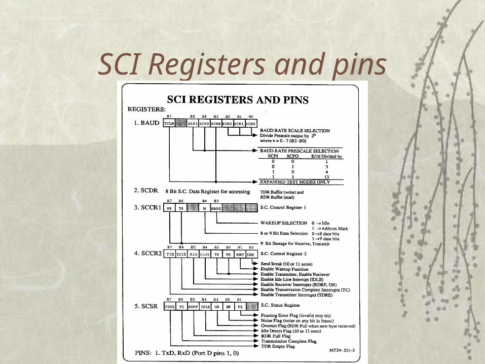
SCI Registers and pins
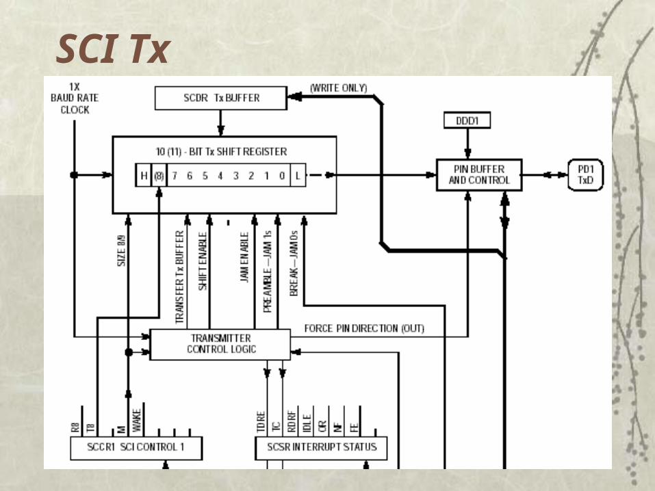
SCI Tx

SCI Rx

SCI configuration
Select desired baud rate -- write to baud rate register (bits SCP0-1, SCR0-2)
Select word length and wake up -- write to SCCR1
Select interrupt operations, TxD and RxD operations, etc. -- write to SCCR2
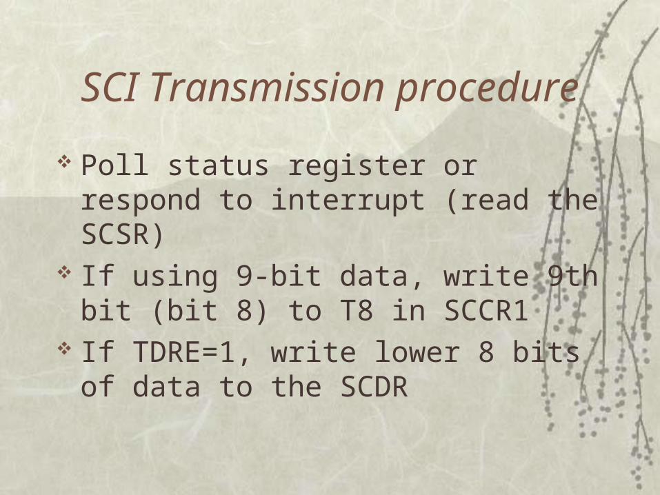
SCI Transmission procedure
Poll status register or respond to interrupt (read the SCSR)
If using 9-bit data, write 9th bit (bit 8) to T8 in SCCR1
If TDRE=1, write lower 8 bits of data to the SCDR

SCI Receiving procedure
Poll status register or react to interrupt (read the SCSR)
If RDRF=1, read SCDR If 9-bit data, read bit 8 from SCCR1

SCI Receive errors Overrun Error
– Occurs when new character is received before previous character is read from SCDR
• New character is lost– Sets OR flag in SCSR
Noise Error– Receiver samples data line at 16 times the bit rate– If samples in middle don’t match, there may be noise on the line– Sets NF flag in SCSR
Framing Error– Occurs when an invalid stop bit is detected
• May be due to baud rate mismatch, framing protocol mismatch, or noise
– Sets FE flag in SCSR

Abstract Data Types

Abstract Data Types Beyond the basic data types
– Unsigned Byte / Word– Signed Byte / Word– Char
Used for modeling Separate parts of a larger programming task
from the rest of the program Allows for better structuring Enables multiple programmers to work on the
same project. Can be used to build libraries with code that can
be incorporated into many different projects

Abstract Data Types: Records A new data type made up of old data types.
record t_POINT { X : signed double Y : signed double}
record t_LINE { begin_pt_x : signed double begin_pt_y : signed double end_pt_x : signed double end_pt_y : signed double}

Abstract Data Types: Records* record POINT_tPOINT_X EQU 0POINT_Y EQU 2POINT_t EQU 4
* MyPoint Global VariableMyPoint: RMB POINT_t
* MyPoint.X <- 5 LDX # MyPoint LDA #5 STA X,POINT_X* MyPoint.Y <- 5 LDA #5 STA X,POINT_Y

Abstract Data TypesContainers
Sequential– FIFO– LIFO (Stack)
Random access– Array

Abstract Data Types: Stacks
Stack– Last-in, first-out (LIFO) structure– Operations
• Push– Places an item on the stack
• Pull– Removes an item from the stack– Some architectures use the term “pop”
– “Bottom” of the stack is at highest memory address, “top” of the stack is at the lowest address
• Stack grows from high to low address

Stack Management
Important to pull data in reverse order that you pushed it
Remember to initialize SP at beginning of program
Note that SP points to empty memory location– Location where next value will be stored

Stack ManagementStack purpose
General data storage (limited) Temporary data storage
• 68HC11 has limited number of registers• Use stack to preserve register values
Example: Multiply ACCA and ACCB, round to 8 bitsPSHB ; save value in ACCBMUL ; ACCD = ACCA*ACCBADCA #$00 ; round to 8 bitsPULB ; restore ACCB
Parameter and control information storage for subroutines
Usually it’s a good idea to embed statistics

State Machines
Capture behavior at high level– Easy to describe and understand.– Well understood theory. – Good supply of simulation and verification
tools.

Statecharts
Statecharts =
FSM +
Hierarchy +
Orthogonality +
Structured transitions +
Broadcast communications

Hierarchy
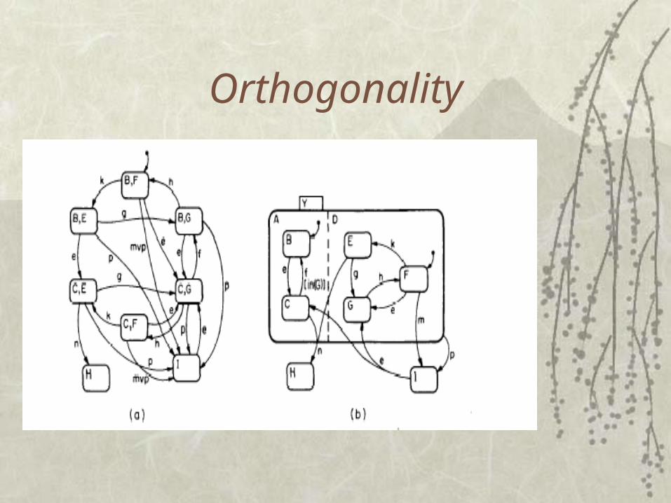
Orthogonality

Broadcast communications
Bus Interfacing and Timing This section focuses on the ability to interface external devices to the
microprocessor Interfacing requires
– Hardware interface -- electrical and mechanical considerations of the interface
– Software interface -- programming necessary to permit the external device and the processor exchange information
The "bus"– The set of signal lines used to connect the processor and the
peripheral devices using read/write operations– Can be a simple extension of the processor pins or can consist of
modifications of the pins – Bus signals can be divided into 3 categories
• Address• Data• Control

Bus Interfacing and Timing
Many microcontrollers use a multiplexed address and data bus– The data bus and (part of) the address bus use
the same physical lines– Address and data signals cannot appear on the
bus at the same time– Requires extra logic to demultiplex
• Usually need to latch the address bits
– Why do we use a multiplexed bus?

General Bus Operation– Processor places desired peripheral's address onto address bus
– Processor (or peripheral) places data onto data bus for a write (read) operation
– Peripheral (processor) gates the data into its internal registers to complete the operation
– Operation is directed by the various control lines that are included in the bus
• Clock signals
• Address strobe / latch
• Device enable signals
• Data direction signals -- read vs. write operations
• Type of reference -- standard or memory mapped I/O -- IO/M*
• Data ready

General Bus Operation
The bus is not a static connection mechanism– Peripheral devices must be enabled (given
access to write to the bus) only when they are participating in a data transfer
– Only 1 device can be driving the bus at any given time -- otherwise bus contention results
• Other devices should be tristated– High-impedance state

General Bus OperationControl signals
Usually an active-low signal Referred to as E*
– Sometimes S* or CS* Device must be enabled before you can write to it or read from it E* is usually derived from address lines Other signals
– R/W*
• May be separate signals
– G*
• Synchronizes data transfer
• Sometimes CLK or E
– Other address lines

General Bus Operation Address decoding
To communicate with a particular peripheral device, the processor places the device's address on the address bus
All peripherals must examine the address and decide if they are being referenced -- address decoding– Usually use digital logic to generate the CS* signal
Two methods of addressing and decoding– Full (exhaustive) decoding
• Each peripheral is assigned to a unique address• All address bits must be used to define the referenced location• Typically used for memory devices

General Bus Operation Address decoding
• Partial decoding– Not all address bits are used in the decoding process
– Peripheral can respond to more than 1 address
– Main advantage is decreased circuit complexity in the decoder
– Disadvantages:• Must guard against inadvertent accesses due to
multiple addresses• Somewhat inefficient use of overall address space

General Bus Operation 68HC11
Modes of operation– Internal parts of MCU
• CPU, memory, registers
– External parts• Pins for I/O and bus signals
– To reduce pin count, some pins may have more than one function
– For HC11, operating mode determines how pins are used
• Select the operating mode using MODA and MODB pins at reset

Single Chip Mode
No external memory or I/O chips– Don’t need external bus– Ports B and C are used as I/O ports
Reduced system cost Limited to on-chip RAM, ROM and
EEPROM

Expanded multiplexed mode
Ports B and C used as address and data bus– Allows connections to external memory and I/O chips
– Port B = A15 - A8
– Port C = AD7-AD0 • A7-A0 multiplexed with D7-D0
Control bus signals– Strobe A/address strobe pin (STRA/AS) used as AS
– Strobe B/read/write pin (STRB/R/W*) used as R/W*

Special bootstrap mode Test mode Generally used to load in a test program, EEPROM
programming, or running a monitor program On reset, HC11 executes code located in the Boot
ROM (BF00-BFFF for 68HC11E9)– Loads more program code using serial interface– Used by PCBUG11– Listing of code in Reference Manual
Special test mode– Intended for use by manufacturer only
• Not much documentation available
– Used to test the chip

Chip Specifications
Appendix A of Technical Data manual– Maximum ratings– Recommended operating conditions– DC electrical characteristics– AC electrical characteristics– Power dissipation
Important when interfacing with other devices– Be aware of
• Current limits• Voltage limits
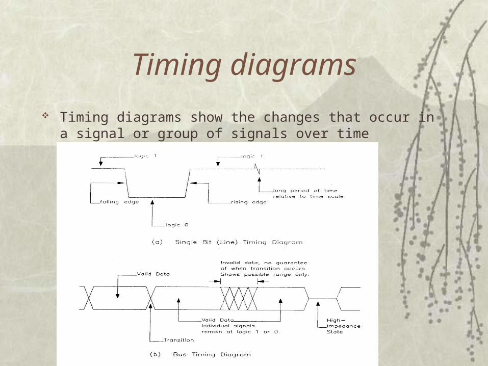
Timing diagrams
Timing diagrams show the changes that occur in a signal or group of signals over time

MemoryOutline
Memory Write Ability and Storage Permanence
Common Memory Types Composing Memory Memory Hierarchy and Cache Advanced RAM
Memory
Stores large number of bits– m x n: m words of n bits each– k = Log2(m) address input signals– or m = 2^k words– e.g., 4,096 x 8 memory:
• 32,768 bits• 12 address input signals• 8 input/output data signals
Memory access– r/w: selects read or write– enable: read or write only when asserted– multiport: multiple accesses to different locations simultaneously

Write abilityStorage permanence
Traditional ROM/RAM distinctions– ROM
• read only, bits stored without power
– RAM• read and write, lose stored bits without power
Traditional distinctions blurred– Advanced ROMs can be written to
• e.g., EEPROM
– Advanced RAMs can hold bits without power• e.g., NVRAM
Write ability– Manner and speed a memory can be written
Storage permanence– ability of memory to hold stored bits after they are written

Classification
Write ability and storage permanence of memories, showing relative degrees along each axis (not to scale).
Externalprogrammer
OR in-system,block-orientedwrites, 1,000s
of cycles
Batterylife (10years)
Writeability
EPROM
Mask-programmed ROM
EEPROM FLASH
NVRAM
SRAM/DRAM
Stor
age
perm
anen
ce
Nonvolatile
In-systemprogrammable
Ideal memory
OTP ROM
Duringfabrication
only
Externalprogrammer,
1,000sof cycles
Externalprogrammer,one time only
Externalprogrammer
OR in-system,1,000s
of cycles
In-system, fastwrites,
unlimitedcycles
Nearzero
Tens ofyears
Life ofproduct

Storage permanence Range of storage permanence
– High end• essentially never loses bits• e.g., mask-programmed ROM
– Middle range• holds bits days, months, or years after memory’s power source turned off• e.g., NVRAM
– Lower range• holds bits as long as power supplied to memory• e.g., SRAM
– Low end• begins to lose bits almost immediately after written• e.g., DRAM
Nonvolatile memory– Holds bits after power is no longer supplied– High end and middle range of storage permanence

ROM
Nonvolatile memory Can be read from but not written to, by a
processor in an embedded system Traditionally written to, “programmed”, before
inserting to embedded system Uses
– Store software program for general-purpose processor• program instructions can be one or more ROM words
– Store constant data needed by system– Implement combinational circuit

ROM Internals
Horizontal lines = words Vertical lines = data Lines connected only at
circles Decoder sets word 2’s line to
1 if address input is 010 Data lines Q3 and Q1 are set to
1 because there is a “programmed” connection with word 2’s line
Word 2 is not connected with data lines Q2 and Q0
Output is 1010
8 × 4 ROM
3×8
decoder
Q0Q3
A0
enable
A2
word 0word 1
A1
Q2 Q1
programmable connection
wired-OR
word line
data line
word 2
Internal view

Mask programmable ROM
Connections “programmed” at fabrication– set of masks
Lowest write ability– only once
Highest storage permanence– bits never change unless damaged
Typically used for final design of high-volume systems– spread out NRE cost for a low unit cost

OTP - ROM
Connections “programmed” after manufacture by user– user provides file of desired contents of ROM– file input to machine called ROM programmer– each programmable connection is a fuse– ROM programmer blows fuses where connections should not exist
Very low write ability– typically written only once and requires ROM programmer device
Very high storage permanence– bits don’t change unless reconnected to programmer and more fuses
blown Commonly used in final products
– cheaper, harder to inadvertently modify

EPROM
Programmable component is a MOS transistor– Transistor has “floating” gate surrounded by an insulator
– (a) Negative charges form a channel between source and drain storing a logic 1
– (b) Large positive voltage at gate causes negative charges to move out of channel and get trapped in floating gate storing a logic 0
– (c) (Erase) Shining UV rays on surface of floating-gate causes negative charges to return to channel from floating gate restoring the logic 1
– (d) An EPROM package showing quartz window through which UV light can pass
Better write ability– can be erased and reprogrammed thousands of times
Reduced storage permanence– program lasts about 10 years but is susceptible to radiation and electric
noise

EEPROM
Programmed and erased electronically– typically by using higher than normal voltage– can program and erase individual words
Better write ability– can be in-system programmable with built-in circuit to provide
higher than normal voltage• built-in memory controller commonly used to hide details from
memory user– writes very slow due to erasing and programming
• “busy” pin indicates to processor EEPROM still writing– can be erased and programmed tens of thousands of times
Similar storage permanence to EPROM (about 10 years) Far more convenient than EPROMs, but more expensive

FLASH
Extension of EEPROM– Same floating gate principle– Same write ability and storage permanence
Fast erase– Large blocks of memory erased at once, rather than one word at a
time– Blocks typically several thousand bytes large
Writes to single words may be slower– Entire block must be read, word updated, then entire block written
back Used with embedded systems storing large data items in nonvolatile
memory– e.g., digital cameras, TV set-top boxes, cell phones

RAM Typically volatile memory
– bits are not held without power supply Read and written to easily by embedded system during execution Internal structure more complex than ROM SRAM: Static RAM
– Memory cell uses flip-flop to store bit– Requires 6 transistors – Holds data as long as power supplied
DRAM: Dynamic RAM– Memory cell uses MOS transistor and capacitor to store bit– More compact than SRAM– “Refresh” required due to capacitor leak
• word’s cells refreshed when read– Typical refresh rate 15.625 microsecond.– Slower to access than SRAM

RAM variations
PSRAM: Pseudo-static RAM– DRAM with built-in memory refresh controller– Popular low-cost high-density alternative to SRAM
NVRAM: Nonvolatile RAM– Holds data after external power removed– Battery-backed RAM
• SRAM with own permanently connected battery• writes as fast as reads• no limit on number of writes unlike nonvolatile ROM-based
memory– SRAM with EEPROM or flash
• stores complete RAM contents on EEPROM or flash before power turned off

Example
Device Access Time (ns) Standby Pwr. (mW) Active Pwr. (mW) Vcc Voltage (V)HM6264 85-100 .01 15 527C256 90 .5 100 5
22
20
data<7…0>
addr<15...0>
/OE
/WE
/CS1
CS2 HM6264
11-13, 15-19
2,23,21,24,25, 3-10
22
27
20
26
data<7…0>
addr<15...0>
/OE
/CS
27C256
11-13, 15-19
27,26,2,23,21,24,25, 3-10
block diagrams
device characteristics
timing diagrams
data
addr
OE
/CS1
CS2
Read operation
data
addr
WE
/CS1
CS2
Write operation
•Low-cost low-capacity memory devices
•Commonly used in 8-bit microcontroller-based embedded systems
•First two numeric digits indicate device type
–RAM: 62
–ROM: 27
•Subsequent digits indicate capacity in kilobits
Combining memory
Memory size needed often differs from size of readily available memories
When available memory is larger, simply ignore unneeded high-order address bits and higher data lines
When available memory is smaller, compose several smaller memories into one larger memory– Connect side-by-side to increase width of words
– Connect top to bottom to increase number of words
• added high-order address line selects smaller memory containing desired word using a decoder
– Combine techniques to increase number and width of words
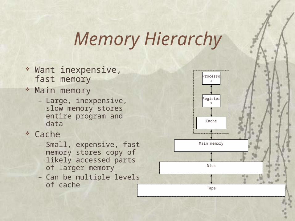
Memory Hierarchy
Want inexpensive, fast memory
Main memory– Large, inexpensive, slow
memory stores entire program and data
Cache– Small, expensive, fast
memory stores copy of likely accessed parts of larger memory
– Can be multiple levels of cache
Processor
Cache
Main memory
Disk
Tape
Registers

Cache
Usually designed with SRAM– faster but more expensive than DRAM
Usually on same chip as processor– space limited, so much smaller than off-chip main memory– faster access ( 1 cycle vs. several cycles for main memory)
Cache operation:– Request for main memory access (read or write)– First, check cache for copy
• cache hit– copy is in cache, quick access
• cache miss– copy not in cache, read address and possibly its neighbors into cache
Several cache design choices– cache mapping, replacement policies, and write techniques

Cache mapping
Much less cache than main memory Are address’ contents in cache? Cache mapping used to assign main memory address to
cache address and determine hit or miss Three basic techniques:
– Direct mapping– Fully associative mapping– Set-associative mapping
Caches partitioned into indivisible blocks or lines of adjacent memory addresses– usually 4 or 8 addresses per line
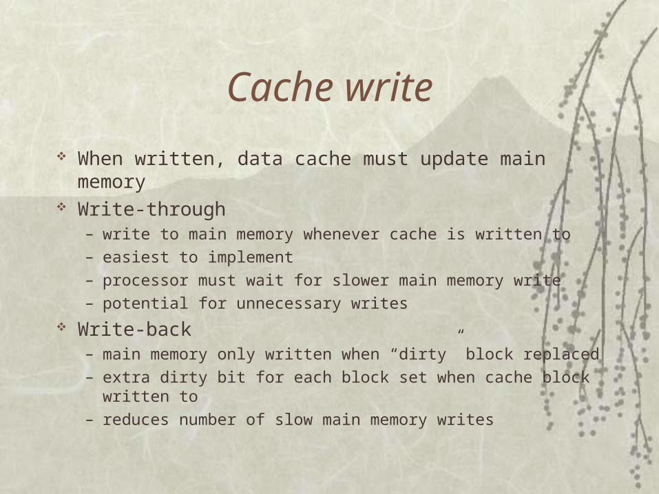
Cache write
When written, data cache must update main memory Write-through
– write to main memory whenever cache is written to
– easiest to implement
– processor must wait for slower main memory write
– potential for unnecessary writes
Write-back– main memory only written when “dirty” block replaced
– extra dirty bit for each block set when cache block written to
– reduces number of slow main memory writes

DRAM
DRAMs commonly used as main memory in processor based embedded systems– high capacity, low cost
Many variations of DRAMs proposed– need to keep pace with processor speeds– FPM DRAM: fast page mode DRAM– EDO DRAM: extended data out DRAM– SDRAM/ESDRAM: synchronous and enhanced
synchronous DRAM– RDRAM: rambus DRAM
Basic DRAM Address bus multiplexed between row and column
components Row and column addresses are latched in,
sequentially, by strobing ras and cas signals, respectively
Refresh circuitry can be external or internal to DRAM device– strobes consecutive memory address periodically
causing memory content to be refreshed
– Refresh circuitry disabled during read or write operation

FPM DRAM Each row of memory bit array is viewed as a page Page contains multiple words Individual words addressed by column address Timing diagram:
– row (page) address sent– 3 words read consecutively by sending column address for each
Extra cycle eliminated on each read/write of words from same page
row col
data
col col
data data
ras
cas
address
data

EDO DRAM
Improvement of FPM DRAM Extra latch before output buffer
– allows strobing of cas before data read operation completed
Reduces read/write latency by additional cycle
row col col col
data data data
Speedup through overlap
ras
cas
address
data

SDRAM SDRAM latches data on active edge of clock Eliminates time to detect ras/cas and rd/wr signals A counter is initialized to column address then
incremented on active edge of clock to access consecutive memory locations
ESDRAM improves SDRAM– added buffers enable overlapping of column addressing– faster clocking and lower read/write latency possible
clock
ras
cas
address
data
row col
data data data

Rambus DRAM (RDRAM)
More of a bus interface architecture than DRAM architecture
Data is latched on both rising and falling edge of clock
Broken into 4 banks each with own row decoder– can have 4 pages open at a time
Capable of very high throughput

MMU
Duties of MMU– Handles DRAM refresh, bus interface and arbitration
– Takes care of memory sharing among multiple processors
– Translates logic memory addresses from processor to physical memory addresses of DRAM
Modern CPUs often come with MMU built-in Single-purpose processors can be used

Assignment
Write program sc_out, sc_in and “echo” in assembly – 15 points
Sc_out – outputs content of A to the SCISc_in – returns received from SCI byte in A
Define behavior of vending machine as statechart – 15 points
For simplicity lets assume it accepts only 1 cent coinUse timeout to take into consideration mechanical delay on delivery
Write program implementing software stack management (stack_init, push, pop) in assembly – 20 points