electronic instrumentation experiment 8: diodes (continued) project 4: optical communications link
TRANSCRIPT
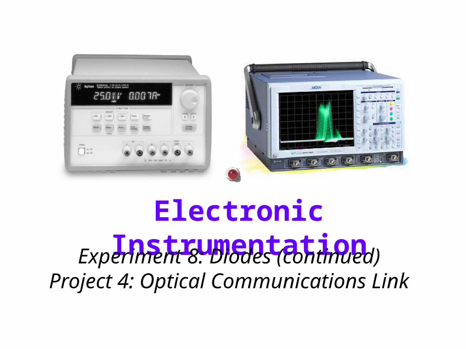
Electronic Instrumentation
Experiment 8: Diodes (continued)Project 4: Optical Communications Link
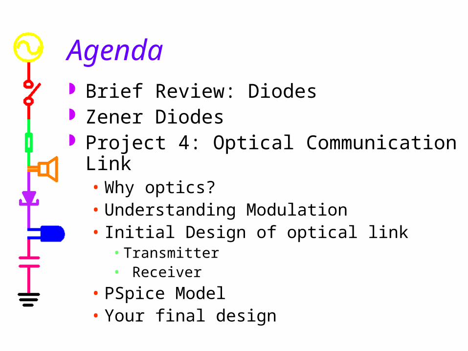
Agenda Brief Review: Diodes Zener Diodes Project 4: Optical Communication Link
• Why optics?• Understanding Modulation• Initial Design of optical link
• Transmitter• Receiver
• PSpice Model• Your final design
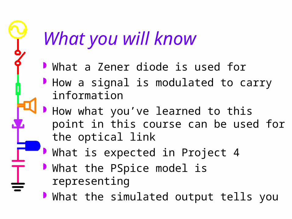
What you will know
What a Zener diode is used for How a signal is modulated to carry
information How what you’ve learned to this point in
this course can be used for the optical link What is expected in Project 4 What the PSpice model is representing What the simulated output tells you

Introduction to Diodes
A diode can be considered to be an electrical one-way valve.
They are made from a large variety of materials including silicon, germanium, gallium arsenide, silicon carbide …
ANODED1
DIODE
CATHODE

Introduction to Diodes
In effect, diodes act like a flapper valve• Note: this is the simplest possible model of a
diode

Introduction to Diodes
Only positivecurrent flows
0
VV
R1
1k
D1
D1N4002V1
FREQ = 1k
VAMPL = 10V
Time
0s 0.5ms 1.0ms 1.5ms 2.0ms 2.5ms 3.0msV(D1:1) V(D1:2)
-10V
-5V
0V
5V
10V

Diode i-v Characteristic Curves
• What is a i-v characteristic curve?
• i-v curve of an ideal diode
• i-v curve of a real diode

i-v characteristic of a real diode Real diode is close to ideal
Ideal Diode

Diode Circuits
• Rectifiers
• Voltage Limiters (Clippers)
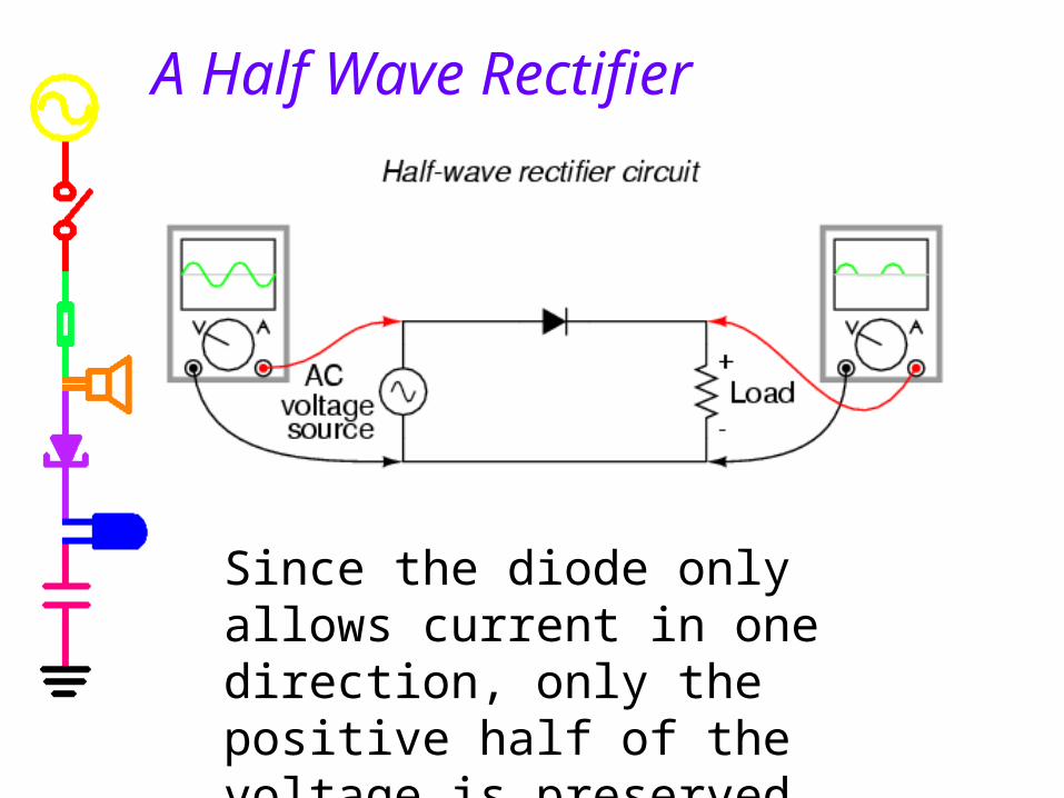
A Half Wave Rectifier
Since the diode only allows current in one direction, only the positive half of the voltage is preserved.
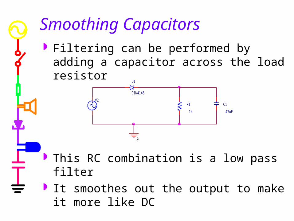
Smoothing Capacitors Filtering can be performed by adding a
capacitor across the load resistor
This RC combination is a low pass filter It smoothes out the output to make it more
like DC
0
R1
1k
D1
D1N4148
V2C1
47uF

A Full Wave Rectifier The rectifier we have just seen is called a half-
wave rectifier since it only uses half of the sinusoidal voltage. A full wave rectifier uses both the negative and positive voltages.

Time
110.0ms 110.5ms 111.0ms 111.5ms 112.0ms 112.5ms 113.0msV(D5:2) V(R4:2,D7:1)
-10V
-5V
0V
5V
10V
A Full Wave Rectifier1.4V (2 diodes)
Note: Since a small voltage drop (around 0.7V) now occurs over two diodes in each direction, the voltage drop from a full wave rectifier is 1.4V.
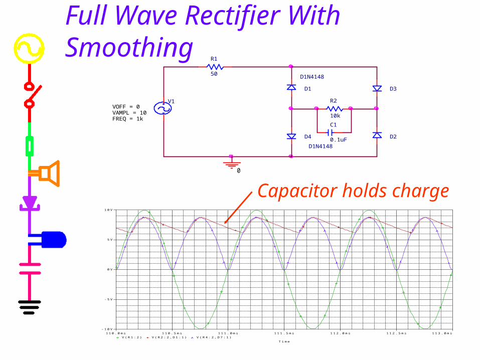
Full Wave Rectifier With Smoothing
D3
D4
D1N4148
C1
0.1uF
R1
50
D2
R2
10k
D1
D1N4148
0
V1
FREQ = 1kVAMPL = 10VOFF = 0
Capacitor holds charge
Time
110.0ms 110.5ms 111.0ms 111.5ms 112.0ms 112.5ms 113.0msV(R1:2) V(R2:2,D1:1) V(R4:2,D7:1)
-10V
-5V
0V
5V
10V
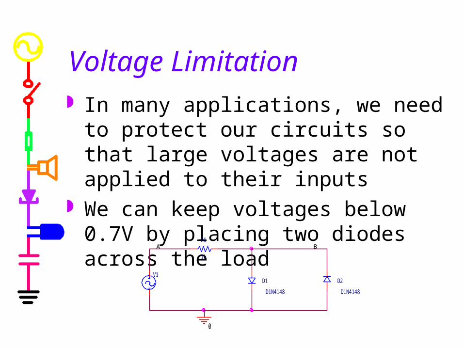
Voltage Limitation In many applications, we need to protect
our circuits so that large voltages are not applied to their inputs
We can keep voltages below 0.7V by placing two diodes across the load
0
V1
R1
1k
D1
D1N4148
D2
D1N4148
A B

Voltage Limitation
Time
0s 0.5ms 1.0ms 1.5ms 2.0ms 2.5ms 3.0msV(R1:1) V(R1:2)
-10V
-5V
0V
5V
10V
(1.2420m,718.277m)
0
D1
D1N4148
VV3
FREQ = 1kVAMPL = 10VOFF = 0 D2
D1N4148
V
R1
1k
Zener Diodes
• Introduction
• i-v curve for a Zener diode
• Zener diode voltage regulation
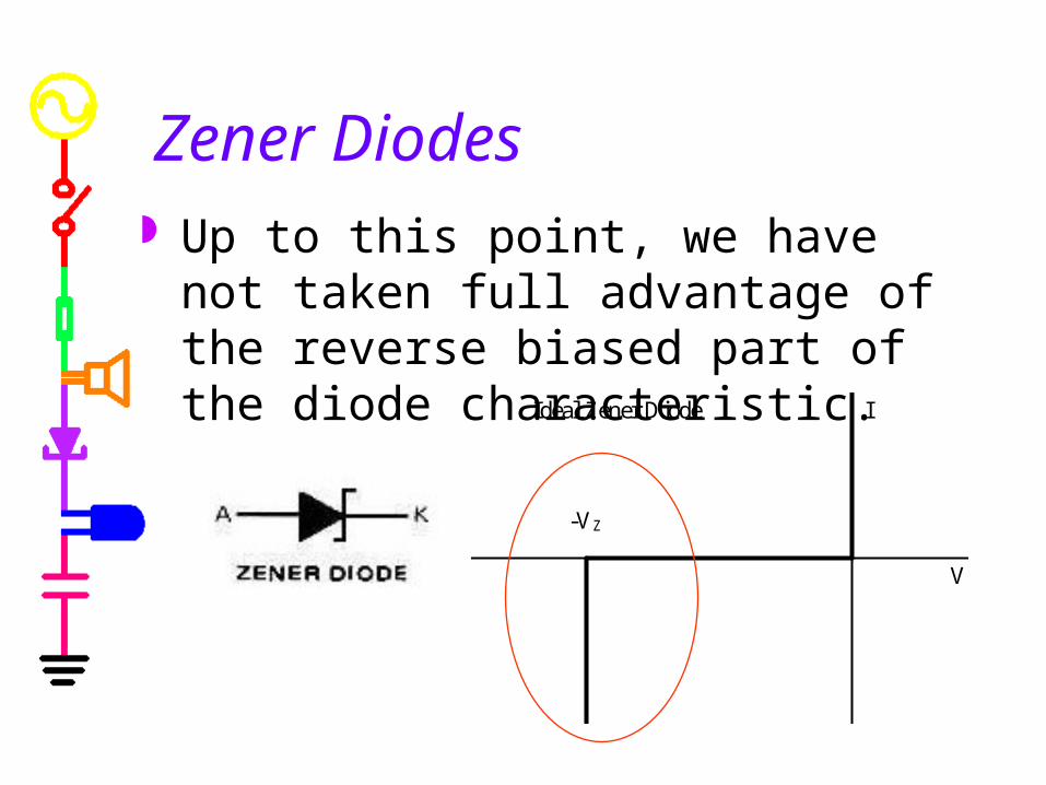
Zener Diodes Up to this point, we have not taken full
advantage of the reverse biased part of the diode characteristic.
Ideal Zener Diode I
-VZ
V

Zener Diodes For the 1N4148 diode, the breakdown voltage is
very large. If we can build a different type of diode with this voltage in a useful range (a few volts to a few hundred volts), we can use such devices to regulate voltages. This type of diode is called a Zener diode because of how the device is made.
Zener diodes are rated according to where they break down. A diode with a Zener voltage (VZ) of 5V, will have a breakdown voltage of -5V.
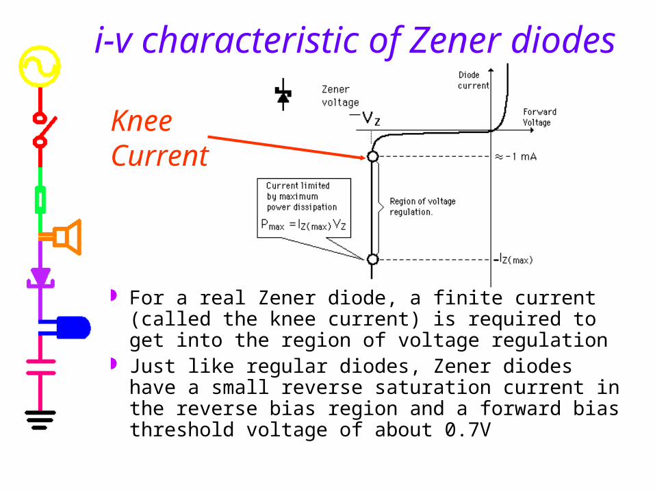
i-v characteristic of Zener diodes
For a real Zener diode, a finite current (called the knee current) is required to get into the region of voltage regulation
Just like regular diodes, Zener diodes have a small reverse saturation current in the reverse bias region and a forward bias threshold voltage of about 0.7V
Knee Current
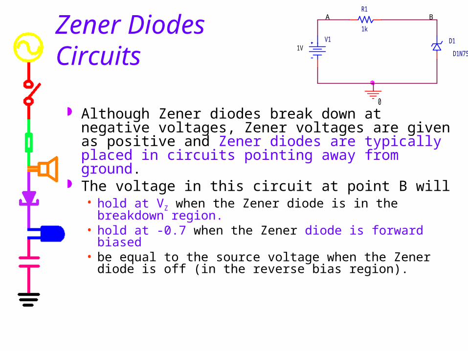
Zener Diodes Circuits
Although Zener diodes break down at negative voltages, Zener voltages are given as positive and Zener diodes are typically placed in circuits pointing away from ground.
The voltage in this circuit at point B will• hold at VZ when the Zener diode is in the breakdown
region.• hold at -0.7 when the Zener diode is forward biased• be equal to the source voltage when the Zener diode is
off (in the reverse bias region).
0
V11V
R1
1k
D1
D1N750
BA
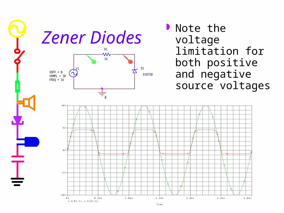
Zener Diodes Note the voltage
limitation for both positive and negative source voltages
D1
D1N750
V1
FREQ = 1kVAMPL = 10VOFF = 0
V V
0
R1
1k
Time
0s 0.5ms 1.0ms 1.5ms 2.0ms 2.5ms 3.0msV(R1:1) V(D1:2)
-10V
-5V
0V
5V
10V
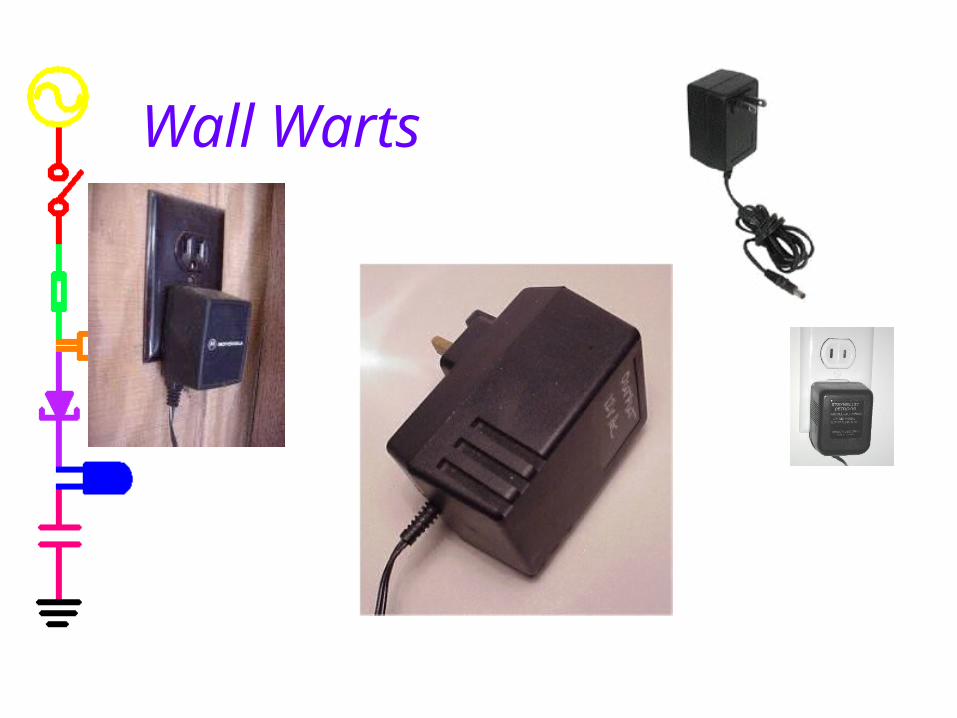
Wall Warts

Transformer Rectifier
Adding a full wave rectifier to the transformer makes a low voltage DC power supply, like the wall warts used on most of the electronics we buy these days.(In reality, VAC is 120Vrms => 170Vpeak)
D2
D1N4148
V
0
V1
FREQ = 60VAMPL = 120VOFF = 0
R1
5
TX1
D4
D1N4148
0
R2
1k
D3
D1N4148
D1
D1N4148C2
33uF
V
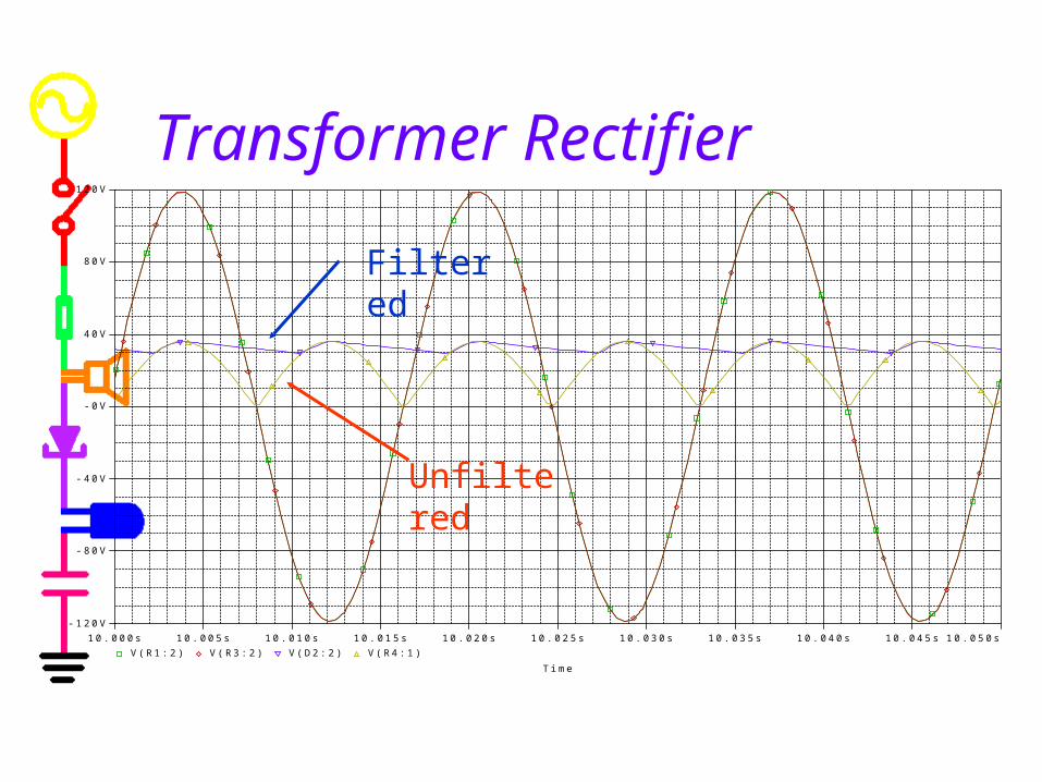
Transformer Rectifier
Time
10.000s 10.005s 10.010s 10.015s 10.020s 10.025s 10.030s 10.035s 10.040s 10.045s 10.050sV(R1:2) V(R3:2) V(D2:2) V(R4:1)
-120V
-80V
-40V
-0V
40V
80V
120V
Filtered
Unfiltered
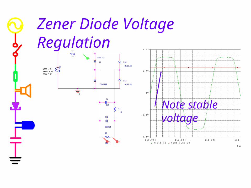
Zener Diode Voltage Regulation
Note stable voltage
Time
110.0ms 110.5ms 111.0ms 111.5ms 112.0ms 112.5ms 113.0msV(D10:1) V(R8:1,R8:2)
-8.0V
-4.0V
0V
4.0V
8.0V
0
C4
1mF
R5
50
D1N4148
D10
D1N4148
R7
10
V+
V3
FREQ = 1kVAMPL = 10VOFF = 0
V-
D9
D1N4148
R8
10k
V
D14
D1N750
D12
D1N4148

Diodes and Light
• Light Emitting Diodes (LEDs)
• Photodiodes and Phototransistors

Light Emitting Diodes• The Light-Emitting Diode
(LED) is a semiconductor pn junction diode that emits visible light or near-infrared radiation when forward biased.
• Visible LEDs emit relatively narrow bands of green, yellow, orange, or red light. Infrared LEDs emit in one of several bands just beyond red light.
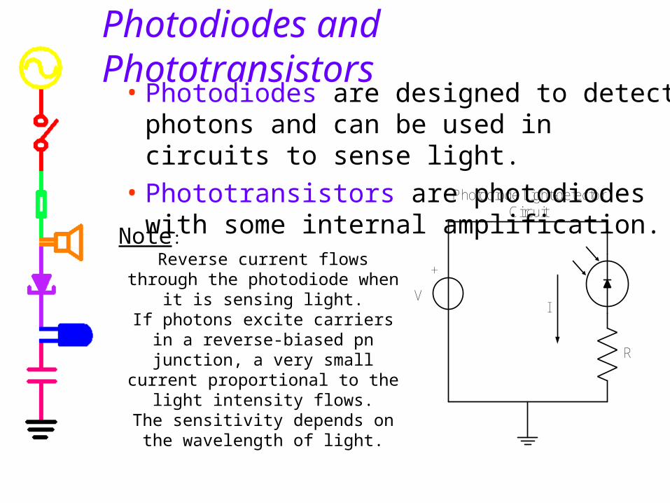
• Photodiodes are designed to detect photons and can be used in circuits to sense light.
• Phototransistors are photodiodes with some internal amplification.
IV
+
R
Photodiode Light-detectorCircuit
Note:Reverse current flows through the photodiode when it is sensing light.
If photons excite carriers in a reverse-biased pn junction, a very small current proportional to the light
intensity flows.The sensitivity depends on the
wavelength of light.
Photodiodes and Phototransistors
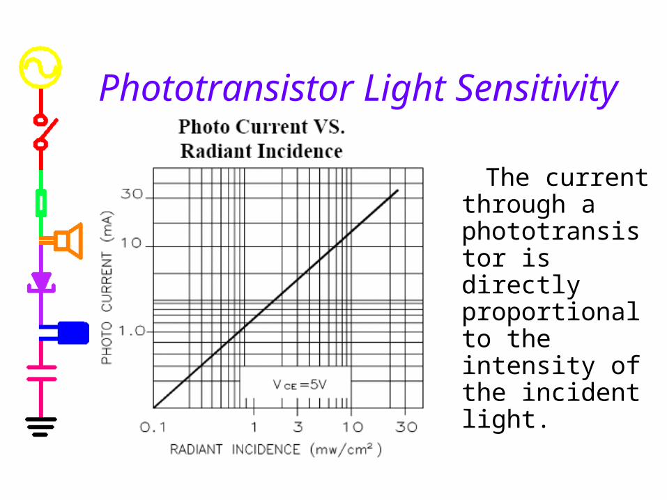
Phototransistor Light Sensitivity
The current through a phototransistor is directly proportional to the intensity of the incident light.
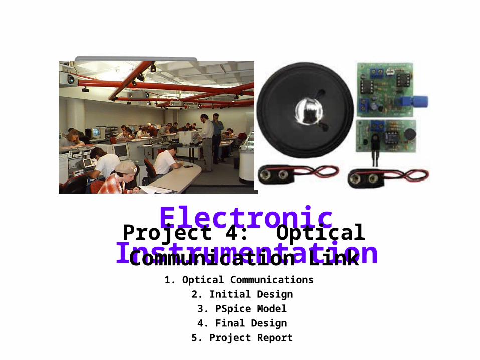
Electronic InstrumentationProject 4: Optical Communication Link
1. Optical Communications
2. Initial Design
3. PSpice Model
4. Final Design
5. Project Report
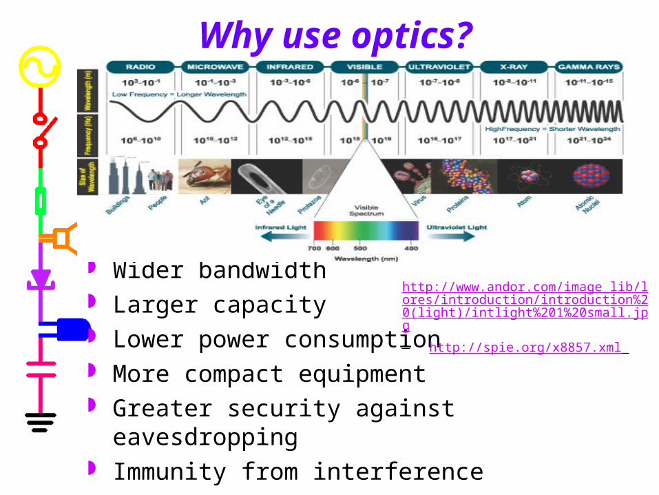
Why use optics? Advantages of optical communication
(over Radio Frequency)
Wider bandwidth Larger capacity Lower power consumption More compact equipment Greater security against eavesdropping Immunity from interference More directed energy
http://www.andor.com/image_lib/lores/introduction/introduction%20(light)/intlight%201%20small.jpg
http://spie.org/x8857.xml

1. Optical Communications

“Lighting the way to a revolution”http://news.bbc.co.uk/1/hi/sci/tech/4671788.stm
The exponential increase of sharing information is largely due to optical communication technology
A few revolutionary technologies based on or effected by optical communication
• Internet (ex. Ethernet LAN based on Infrared Technology)
• Cell phones
• Satellite communication Others?
1966 Dr. Kao andGeorge Hockham:
fiber optics to carry information with light

Transmitting an audio signal using light
Receiver Circuit
Transmitter Circuit
In free space (air)

Modulation Modulation is a way to encode an
electromagnetic signal so that it can be transmitted and received.
A carrier signal (constant) is changed by the transmitter in some way based on the information to be sent.
The receiver then recreates the signal by looking at how the carrier was changed.

Modulation
Output (modulated carrier) depends on the type of modulation used
ModulatingInput signal
Carriersignal
Time
0s 4.0msV(R2:1) V(R1:1)
-4.0V
-3.0V
-2.0V
-1.0V
0V
1.0V
2.0V
3.0V
4.0V
5.0V
6.0V
7.0V
8.0V
Modulation Types
General• Frequency Modulation• Amplitude Modulation
Pulse• Pulse Width Modulation• Pulse Position Modulation• Pulse Frequency Modulation
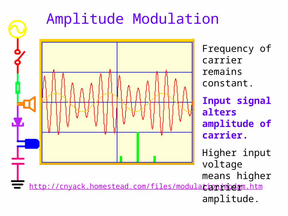
Amplitude Modulation
http://cnyack.homestead.com/files/modulation/modam.htm
Frequency of carrier remains constant.
Input signal alters amplitude of carrier.
Higher input voltage means higher carrier amplitude.

Frequency Modulation
http://cnyack.homestead.com/files/modulation/modfm.htm
Amplitude of carrier remains constant.
Input signal alters frequency of carrier.
Higher input voltage means higher carrier frequency.

Pulse Modulation Remember duty cycle definition and equation
Carrier has a constant variable• Pulse Width Modulation - Period is constant• Pulse Position Modulation - Pulse width is constant• Pulse Frequency Modulation - Duty cycle is constant
Input modulates carrier and effects other two variables
T
TonCycleDuty _
Ton
Toff
Period
widthPulseCycleDuty
__ ToffTonT

Pulse Width Modulation
http://cnyack.homestead.com/files/modulation/modpwm.htm
Period of carrier remains constant.
Input signal alters duty cycle and pulse width of carrier.
Higher input voltage means pulses with longer pulse widths and higher duty cycles.

Pulse Position Modulation
http://cnyack.homestead.com/files/modulation/modppm.htm
Pulse width of carrier remains constant.
Input signal alters period and duty cycle of carrier.
Higher input voltage means pulses with longer periods and lower duty cycles.

Pulse Frequency ModulationDuty cycle of carrier remains constant.
Input signal alters pulse width and period of carrier.
Higher input voltage means pulses with longer pulse widths and longer periods.

2. Initial Design
The initial design for this project is a circuit consisting of a transmitter and a receiver.
The circuit is divided into functional blocks.• Transmitter: Block A-B and Block B-C• Transmission: Block C-D• Receiver: Block D-E, Block E-F, Block F-G, and Block G-H
You will need to examine each block of the circuit.
transmitter receiver
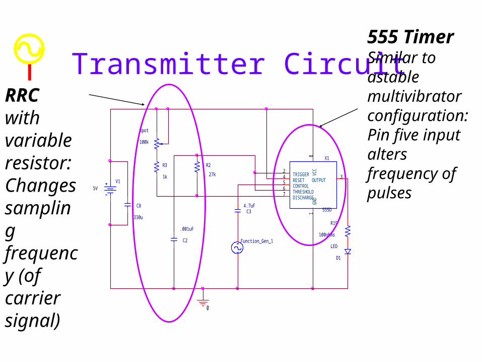
Transmitter Circuit
X1
555D
GND
1
TRIGGER2
OUTPUT3
RESET4
CONTROL5
THRESHOLD6
DISCHARGE7
VCC
8
R2
27k
R3
1k
C2
.001uF
C34.7uF
V15V
Function_Gen_1
C8
330uR19
100ohms
D1
LED
0
Rpot
100k
555 Timer Similar to astable multivibrator configuration:Pin five input alters frequency of pulses
RRCwith variable resistor:Changes sampling frequency (of carrier signal)

X1
555D
GND
1
TRIGGER2
OUTPUT3
RESET4
CONTROL5
THRESHOLD6
DISCHARGE7
VCC
8
R2
27k
R3
1k
C2
.001uF
C34.7uF
V15V
Function_Gen_1
C8
330uR19
100ohms
D1
LED
0
Rpot
100k
Transmitter Circuit:Input and Modulated Output
Input signal: function generator or audio
Output signal:Light modulationfrom LED

X1
555D
GND
1
TRIGGER2
OUTPUT3
RESET4
CONTROL5
THRESHOLD6
DISCHARGE7
VCC
8
R2
27k
R3
1k
C2
.001uF
C34.7uF
V15V
Function_Gen_1
C8
330uR19
100ohms
D1
LED
0
Rpot
100k
Special Capacitors
Bypass Capacitor(Low Pass Filter)
DC Blocking Capacitor(High Pass Filter)Keeps DC offset from 555 Timerfrom interfering with input

Sample Input and Output
When input is higher, pulses are longer When input is lower, pulses are shorter
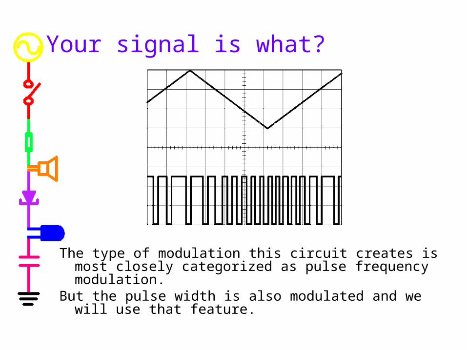
Your signal is what?
The type of modulation this circuit creates is most closely categorized as pulse frequency modulation.
But the pulse width is also modulated and we will use that feature.

Sampling Frequency
The pot (used as a variable resistor) controls your sampling frequency
Input frequency in audible range • max range (20 - 20kHz)
• representative range (500 - 4kHz)
Sampling frequency should be between 8kHz and 48kHz to reconstruct sound
Input amplitude should not exceed 2Vp-p• Function generator can provide 1.2Vp-p

Receiver Circuit
56k
Add a 100 Ohm resistor in series with the speaker to avoid failures.
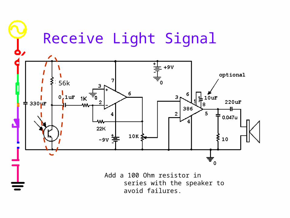
Receive Light Signal
56k
Add a 100 Ohm resistor in series with the speaker to avoid failures.

Inverting Amplifier (Pre-Amp)
56k
Add a 100 Ohm resistor in series with the speaker to avoid failures.

Audio Amplifier
Add a 100 Ohm resistor in series with the speaker to avoid failures.
56k
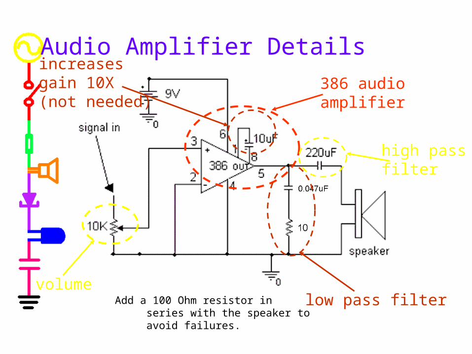
Audio Amplifier Details
volume
386 audioamplifier
low pass filter
high passfilter
increasesgain 10X(not needed)
Add a 100 Ohm resistor in series with the speaker to avoid failures.
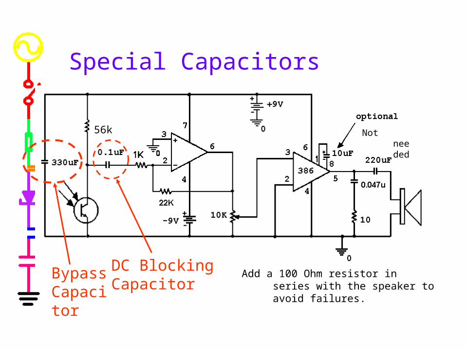
Special Capacitors
BypassCapacitor
DC BlockingCapacitor
Add a 100 Ohm resistor in series with the speaker to avoid failures.
Not needed56k
3. PSpice Model
You will compare the performance of your circuit to a PSpice model.
The PSpice for the initial design will be given to you.
You will use the PSpice to help you make decisions about how to create your final design.


Comparing Output of Blocks
Take pictures of the signal on each side of the circuit block.• A on channel 1 and B on channel 2• B on channel 1 and C on channel 2
Take all measurements relative to ground Does the block behave as expected? How does it compare to the PSpice output?

Comparing Output of Blocks
Time
8.0ms 8.4ms 8.8ms 9.2ms 9.6ms 10.0msV(R1:1) V(L1:2)
-5V
0V
5V
10V
“close-up” view Output divided
by 10 Shows sampling
frequency Shows shape of
samples
Time
8.400ms 8.500ms 8.600ms 8.700ms8.301ms 8.799msV(R1:1) V(L1:2)/10
-1.0V
0V
1.0V
“wide-angle” view Shows overall
shape and size of input and output
4. Final Design
The signal is reconstructed well enough by the initial design that it will be audible.
In order to improve the quality of the signal, you will add an integrator, which will more exactly reconstruct it.
Types of integrators• passive integrator (low pass filter)• active integrator (op amp integrator circuit)
You will then improve the signal further with a smoothing capacitor.
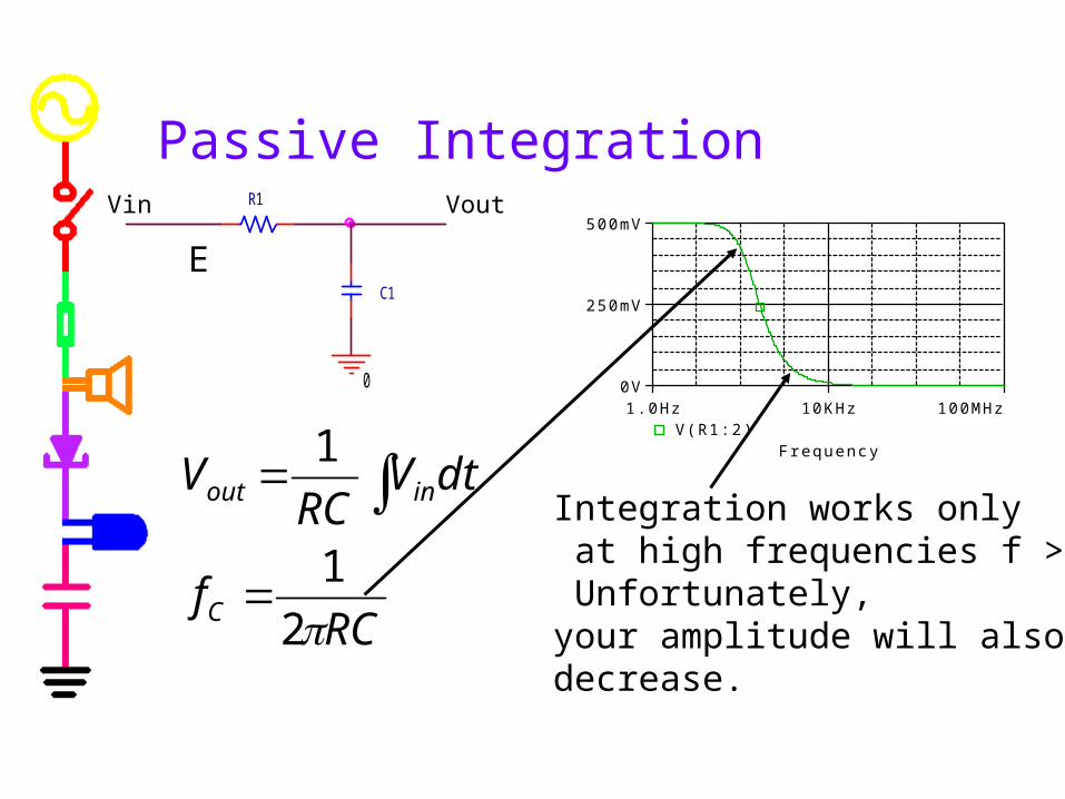
Passive Integration
C1
R1 VoutVin
0
Integration works only at high frequencies f >>fc. Unfortunately,your amplitude will alsodecrease.
RCf
dtVRC
V
C
inout
2
1
1
Frequency
1.0Hz 10KHz 100MHzV(R1:2)
0V
250mV
500mV
E
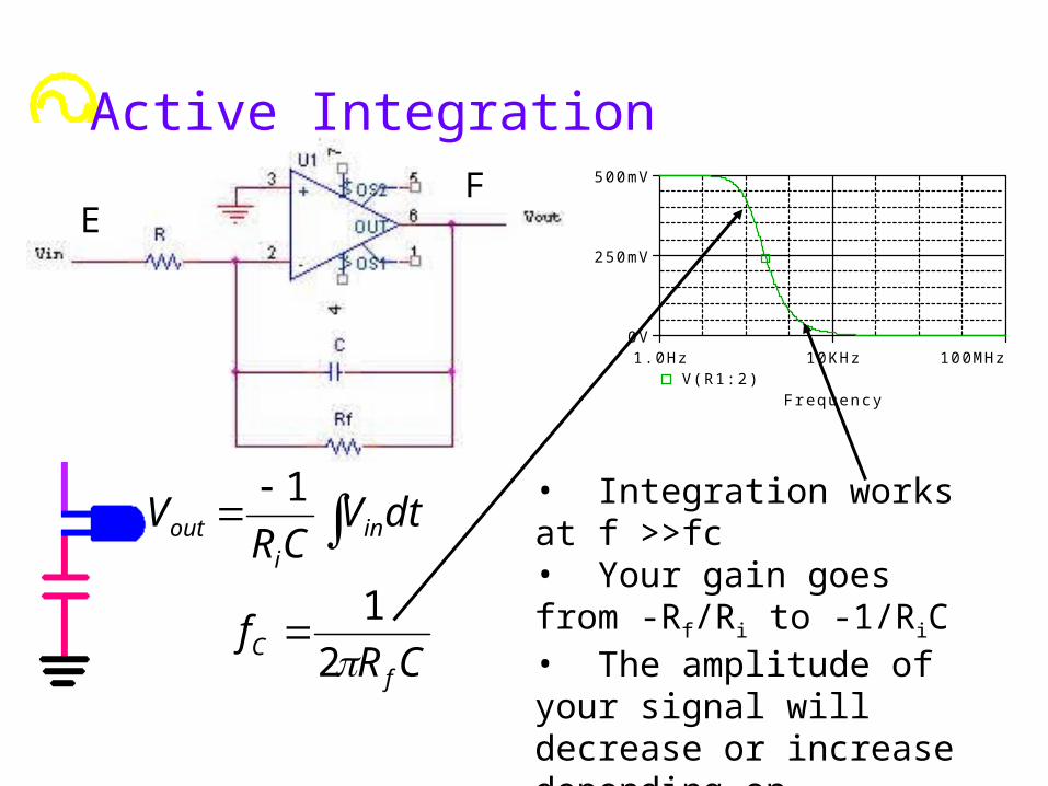
Active Integration
CRf
dtVCR
V
fC
ini
out
2
1
1
• Integration works at f >>fc• Your gain goes from -Rf/Ri to -1/RiC• The amplitude of your signal will decrease or increase depending on components
Frequency
1.0Hz 10KHz 100MHzV(R1:2)
0V
250mV
500mV
EF
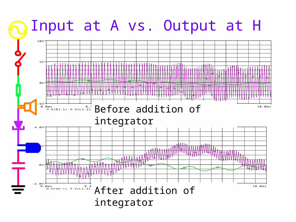
Input at A vs. Output at H
Time
8.0ms 8.4ms 8.8ms 9.2ms 9.6ms 10.0msV(R1:1) V(L1:2)
-5V
0V
5V
10V
Time
8.0ms 8.4ms 8.8ms 9.2ms 9.6ms 10.0msV(V4:+) V(L1:2)
-2.0V
0V
2.0V
4.0V
Before addition of integrator
After addition of integrator

Effect of Smoothing Capacitor
Recall what the smoothing capacitor did to the output of the half wave rectifier.
0
V
D1
D1N4148V
V1
FREQ = 1kVAMPL = 5vVOFF = 0 C1
5u
R1
1k
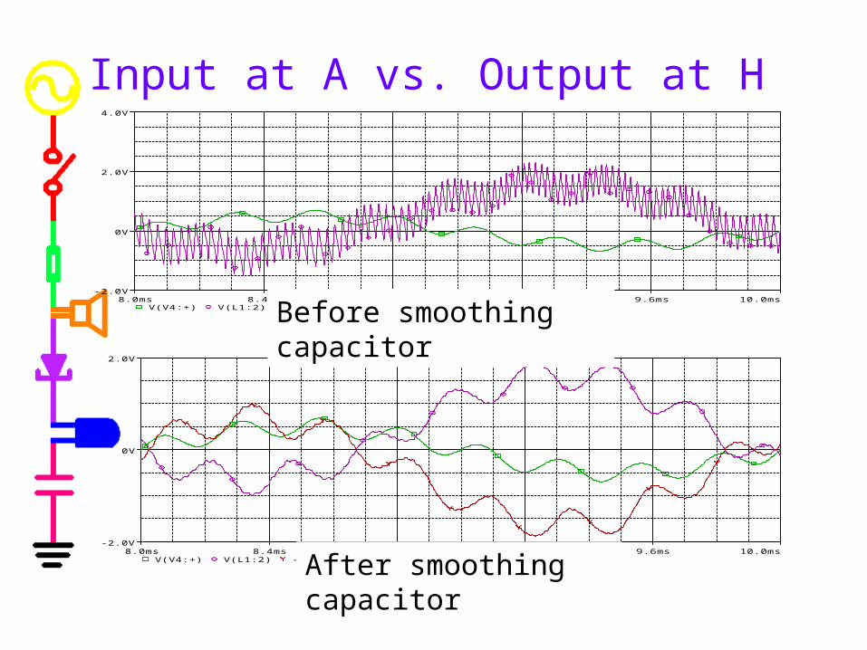
Time
8.0ms 8.4ms 8.8ms 9.2ms 9.6ms 10.0msV(V4:+) V(L1:2)
-2.0V
0V
2.0V
4.0V
Time
8.0ms 8.4ms 8.8ms 9.2ms 9.6ms 10.0msV(V4:+) V(L1:2) -v(L1:2)
-2.0V
0V
2.0V
Input at A vs. Output at H
Before smoothing capacitor
After smoothing capacitor

Project Packet Initial Data with Function Generator
• PSpice• Mobile Studio plots from circuit• Brief Comparison• Block Description• For
• Blocks: A-B, A-C, A-D, A-E, A-F, A-G• Overall System: A-H
Initial Data with Audio• Mobile Studio plots from circuit• For E-F and A-H
Project Packet Final Data (integrator only) with Function
Generator• PSpice• Mobile Studio plots from circuit• Brief Comparison• For E-F and A-H
Final Data (integrator and smoothing) PSpice only• PSpice• Compare to without smoothing• For E-F and A-H
Project Packet Final Data with Integrator (and possibly
Smoothing) with Audio• Mobile Studio plots from circuit
• For E-F and A-H
Extra Credit• Mobile Studio picture of A-H with input from function
generator and integrated, smoothed output. Indicate values of components and where used.
Work in teams Put the transmitter on one protoboard and the
receiver on a second.• One pair do the transmitter circuit
• This is the easier circuit, so maybe also start the PSpice simulation.
• The other pair build the receiver circuit
One report for the entire team• Report is closer to an experiment report than a project
report
• See details in handout.