electromagnetics of metals - amolf electromagnetics of metals low-frequency regime, the perfect or...
TRANSCRIPT

Chapter 1
ELECTROMAGNETICS OF METALS
While the optical properties of metals are discussed in most textbooks oncondensed matter physics, for convenience this chapter summarizes the mostimportant facts and phenomena that form the basis for a study of surface plas-mon polaritons. Starting with a cursory review of Maxwell’s equations, wedescribe the electromagnetic response both of idealized and real metals over awide frequency range, and introduce the fundamental excitation of the conduc-tion electron sea in bulk metals: volume plasmons. The chapter closes with adiscussion of the electromagnetic energy density in dispersive media.
1.1 Maxwell’s Equations and Electromagnetic WavePropagation
The interaction of metals with electromagnetic fields can be firmly under-stood in a classical framework based on Maxwell’s equations. Even metallicnanostructures down to sizes on the order of a few nanometres can be describedwithout a need to resort to quantum mechanics, since the high density of freecarriers results in minute spacings of the electron energy levels compared tothermal excitations of energy kBT at room temperature. The optics of met-als described in this book thus falls within the realms of the classical theory.However, this does not prevent a rich and often unexpected variety of opticalphenomena from occurring, due to the strong dependence of the optical prop-erties on frequency.
As is well known from everyday experience, for frequencies up to the vis-ible part of the spectrum metals are highly reflective and do not allow elec-tromagnetic waves to propagate through them. Metals are thus traditionallyemployed as cladding layers for the construction of waveguides and resonatorsfor electromagnetic radiation at microwave and far-infrared frequencies. In this

6 Electromagnetics of Metals
low-frequency regime, the perfect or good conductor approximation of infiniteor fixed finite conductivity is valid for most purposes, since only a negligiblefraction of the impinging electromagnetic waves penetrates into the metal. Athigher frequencies towards the near-infrared and visible part of the spectrum,field penetration increases significantly, leading to increased dissipation, andprohibiting a simple size scaling of photonic devices that work well at lowfrequencies to this regime. Finally, at ultraviolet frequencies, metals acquiredielectric character and allow the propagation of electromagnetic waves, albeitwith varying degrees of attenuation, depending on the details of the electronicband structure. Alkali metals such as sodium have an almost free-electron-likeresponse and thus exhibit an ultraviolet transparency. For noble metals suchas gold or silver on the other hand, transitions between electronic bands leadto strong absorption in this regime.
These dispersive properties can be described via a complex dielectric func-tion ε(ω), which provides the basis of all phenomena discussed in this text.The underlying physics behind this strong frequency dependence of the opticalresponse is a change in the phase of the induced currents with respect to thedriving field for frequencies approaching the reciprocal of the characteristicelectron relaxation time τ of the metal, as will be discussed in section 1.2.
Before presenting an elementary description of the optical properties of met-als, we recall the basic equations governing the electromagnetic response, themacroscopic Maxwell equations. The advantage of this phenomenological ap-proach is that details of the fundamental interactions between charged parti-cles inside media and electromagnetic fields need not be taken into account,since the rapidly varying microscopic fields are averaged over distances muchlarger than the underlying microstructure. Specifics about the transition froma microscopic to a macroscopic description of the electromagnetic response ofcontinuous media can be found in most textbooks on electromagnetics such as[Jackson, 1999].
We thus take as a starting point Maxwell’s equations of macroscopic elec-tromagnetism in the following form:
∇ · D = ρext (1.1a)
∇ · B = 0 (1.1b)
∇ × E = −∂B∂t
(1.1c)
∇ × H = Jext + ∂D∂t
. (1.1d)
These equations link the four macroscopic fields D (the dielectric displace-ment), E (the electric field), H (the magnetic field), and B (the magnetic induc-

Maxwell’s Equations and Electromagnetic Wave Propagation 7
tion or magnetic flux density) with the external charge and current densitiesρext and Jext. Note that we do not follow the usual procedure of presenting themacroscopic equations via dividing the total charge and current densities ρtot
and Jtot into free and bound sets, which is an arbitrary division [Illinskii andKeldysh, 1994] and can (especially in the case of metallic interfaces) confusethe application of the boundary condition for the dielectric displacement. In-stead, we distinguish between external (ρext, Jext) and internal (ρ, J) chargeand current densities, so that in total ρtot = ρext + ρ and Jtot = Jext + J. Theexternal set drives the system, while the internal set responds to the externalstimuli [Marder, 2000].
The four macroscopic fields are further linked via the polarization P andmagnetization M by
D = ε0E + P (1.2a)
H = 1
μ0B − M, (1.2b)
where ε0 and μ0 are the electric permittivity1 and magnetic permeability2 ofvacuum, respectively. Since we will in this text only treat nonmagnetic me-dia, we need not consider a magnetic response represented by M, but can limitour description to electric polarization effects. P describes the electric dipolemoment per unit volume inside the material, caused by the alignment of micro-scopic dipoles with the electric field. It is related to the internal charge densityvia ∇ · P = −ρ. Charge conservation (∇ · J = −∂ρ/∂t) further requires thatthe internal charge and current densities are linked via
J = ∂P∂t
. (1.3)
The great advantage of this approach is that the macroscopic electric fieldincludes all polarization effects: In other words, both the external and the in-duced fields are absorbed into it. This can be shown via inserting (1.2a) into(1.1a), leading to
∇ · E = ρtot
ε0. (1.4)
In the following, we will limit ourselves to linear, isotropic and nonmagneticmedia. One can define the constitutive relations
D = ε0εE (1.5a)
B = μ0μH. (1.5b)
1ε0 ≈ 8.854 × 10⁻¹² F/m2μ0 ≈ 1.257 × 10⁻⁶ H/m

8 Electromagnetics of Metals
ε is called the dielectric constant or relative permittivity and μ = 1 the rela-tive permeability of the nonmagnetic medium. The linear relationship (1.5a)between D and E is often also implicitly defined using the dielectric suscepti-bility χ (particularly in quantum mechanical treatments of the optical response[Boyd, 2003]), which describes the linear relationship between P and E via
P = ε0χE. (1.6)
Inserting (1.2a) and (1.6) into (1.5a) yields ε = 1 + χ .The last important constitutive linear relationship we need to mention is that
between the internal current density J and the electric field E, defined via theconductivity σ by
J = σE. (1.7)
We will now show that there is an intimate relationship between ε and σ ,and that electromagnetic phenomena with metals can in fact be described usingeither quantity. Historically, at low frequencies (and in fact in many theoreticalconsiderations) preference is given to the conductivity, while experimentalistsusually express observations at optical frequencies in terms of the dielectricconstant. However, before embarking on this we have to point out that thestatements (1.5a) and (1.7) are only correct for linear media that do not exhibittemporal or spatial dispersion. Since the optical response of metals clearlydepends on frequency (possibly also on wave vector), we have to take accountof the non-locality in time and space by generalizing the linear relationships to
D(r, t) = ε0
∫dt ′dr′ε(r − r′, t − t ′)E(r′, t ′) (1.8a)
J(r, t) =∫
dt ′dr′σ(r − r′, t − t ′)E(r′, t ′). (1.8b)
ε0ε and σ therefore describe the impulse response of the respective linear re-lationship. Note that we have implicitly assumed that all length scales aresignificantly larger than the lattice spacing of the material, ensuring homo-geneity, i.e. the impulse response functions do not depend on absolute spatialand temporal coordinates, but only their differences. For a local response, thefunctional form of the impulse response functions is that of a δ-function, and(1.5a) and (1.7) are recovered.
Equations (1.8) simplify significantly by taking the Fourier transform withrespect to
∫dtdrei(K·r−ωt), turning the convolutions into multiplications. We
are thus decomposing the fields into individual plane-wave components ofwave vector K and angular frequency ω. This leads to the constitutive rela-

Maxwell’s Equations and Electromagnetic Wave Propagation 9
tions in the Fourier domain
D(K, ω) = ε0ε(K, ω)E(K, ω) (1.9a)
J(K, ω) = σ(K, ω)E(K, ω). (1.9b)
Using equations (1.2a), (1.3) and (1.9) and recognizing that in the Fourier do-main ∂/∂t → −iω, we finally arrive at the fundamental relationship betweenthe relative permittivity (from now on called the dielectric function) and theconductivity
ε(K, ω) = 1 + iσ (K, ω)
ε0ω. (1.10)
In the interaction of light with metals, the general form of the dielectric re-sponse ε(ω, K) can be simplified to the limit of a spatially local response viaε(K = 0, ω) = ε(ω). The simplification is valid as long as the wavelength λ
in the material is significantly longer than all characteristic dimensions such asthe size of the unit cell or the mean free path of the electrons. This is in generalstill fulfilled at ultraviolet frequencies3.
Equation (1.10) reflects a certain arbitrariness in the separation of chargesinto bound and free sets, which is entirely due to convention. At low frequen-cies, ε is usually used for the description of the response of bound charges to adriving field, leading to an electric polarization, while σ describes the contri-bution of free charges to the current flow. At optical frequencies however, thedistinction between bound and free charges is blurred. For example, for highly-doped semiconductors, the response of the bound valence electrons could belumped into a static dielectric constant δε, and the response of the conductionelectrons into σ ′, leading to a dielectric function ε(ω) = δε + iσ ′(ω)
ε0ω. A simple
redefinition δε → 1 and σ ′ → σ ′ + ε0ω
iδε will then result in the general form
(1.10) [Ashcroft and Mermin, 1976].In general, ε(ω) = ε1(ω)+iε2(ω) and σ(ω) = σ1(ω)+iσ2(ω) are complex-
valued functions of angular frequency ω, linked via (1.10). At optical frequen-cies, ε can be experimentally determined for example via reflectivity studiesand the determination of the complex refractive index n(ω) = n(ω) + iκ(ω)
of the medium, defined as n = √ε. Explicitly, this yields
3However, spatial dispersion effects can lead to small corrections for surface plasmons polaritons in metallicnanostructures significantly smaller than the electron mean free path, which can arise for example at the tipof metallic cones (see chapter 7).

10 Electromagnetics of Metals
ε1 = n2 − κ2 (1.11a)
ε2 = 2nκ (1.11b)
n2 = ε1
2+ 1
2
√ε2
1 + ε22 (1.11c)
κ = ε2
2n. (1.11d)
κ is called the extinction coefficient and determines the optical absorption ofelectromagnetic waves propagating through the medium. It is linked to theabsorption coefficient α of Beer’s law (describing the exponential attenuationof the intensity of a beam propagating through the medium via I (x) = I0e
−αx)by the relation
α(ω) = 2κ(ω)ω
c. (1.12)
Therefore, the imaginary part ε2 of the dielectric function determines theamount of absorption inside the medium. For |ε1| � |ε2|, the real part n
of the refractive index, quantifying the lowering of the phase velocity of thepropagating waves due to polarization of the material, is mainly determined byε1. Examination of (1.10) thus reveals that the real part of σ determines theamount of absorption, while the imaginary part contributes to ε1 and thereforeto the amount of polarization.
We close this section by examining traveling-wave solutions of Maxwell’sequations in the absence of external stimuli. Combining the curl equations(1.1c), (1.1d) leads to the wave equation
∇ × ∇ × E = −μ0∂2D∂t2
(1.13a)
K(K · E) − K2E = −ε(K, ω)ω2
c2E, (1.13b)
in the time and Fourier domains, respectively. c = 1√ε0μ0
is the speed of lightin vacuum. Two cases need to be distinguished, depending on the polarizationdirection of the electric field vector. For transverse waves, K · E = 0, yieldingthe generic dispersion relation
K2 = ε(K, ω)ω2
c2. (1.14)
For longitudinal waves, (1.13b) implies that
ε(K, ω) = 0, (1.15)

The Dielectric Function of the Free Electron Gas 11
signifying that longitudinal collective oscillations can only occur at frequenciescorresponding to zeros of ε(ω). We will return to this point in the discussionof volume plasmons in section 1.3.
1.2 The Dielectric Function of the Free Electron GasOver a wide frequency range, the optical properties of metals can be ex-
plained by a plasma model, where a gas of free electrons of number densityn moves against a fixed background of positive ion cores. For alkali metals,this range extends up to the ultraviolet, while for noble metals interband transi-tions occur at visible frequencies, limiting the validity of this approach. In theplasma model, details of the lattice potential and electron-electron interactionsare not taken into account. Instead, one simply assumes that some aspects ofthe band structure are incorporated into the effective optical mass m of eachelectron. The electrons oscillate in response to the applied electromagneticfield, and their motion is damped via collisions occurring with a characteristiccollision frequency γ = 1/τ . τ is known as the relaxation time of the freeelectron gas, which is typically on the order of 10−14 s at room temperature,corresponding to γ = 100 THz.
One can write a simple equation of motion for an electron of the plasma seasubjected to an external electric field E:
mx + mγ x = −eE (1.16)
If we assume a harmonic time dependence E(t) = E0e−iωt of the driving field,a particular solution of this equation describing the oscillation of the electronis x(t) = x0e−iωt . The complex amplitude x0 incorporates any phase shiftsbetween driving field and response via
x(t) = e
m(ω2 + iγ ω)E(t). (1.17)
The displaced electrons contribute to the macroscopic polarization P = −nex,explicitly given by
P = − ne2
m(ω2 + iγ ω)E. (1.18)
Inserting this expression for P into equation (1.2a) yields
D = ε0(1 − ω2p
ω2 + iγ ω)E, (1.19)
where ω2p = ne2
ε0mis the plasma frequency of the free electron gas. Therefore we
arrive at the desired result, the dielectric function of the free electron gas:

12 Electromagnetics of Metals
ε(ω) = 1 − ω2p
ω2 + iγ ω. (1.20)
The real and imaginary components of this complex dielectric function ε(ω) =ε1(ω) + iε2(ω) are given by
ε1(ω) = 1 − ω2pτ
2
1 + ω2τ 2(1.21a)
ε2(ω) = ω2pτ
ω(1 + ω2τ 2), (1.21b)
where we have used γ = 1/τ . It is insightful to study (1.20) for a variety ofdifferent frequency regimes with respect to the collision frequency γ . We willlimit ourselves here to frequencies ω < ωp, where metals retain their metalliccharacter. For large frequencies close to ωp, the product ωτ � 1, leading tonegligible damping. Here, ε(ω) is predominantly real, and
ε(ω) = 1 − ω2p
ω2(1.22)
can be taken as the dielectric function of the undamped free electron plasma.Note that the behavior of noble metals in this frequency region is completelyaltered by interband transitions, leading to an increase in ε2. The examples ofgold and silver will be discussed below and in section 1.4.
We consider next the regime of very low frequencies, where ω � τ−1.Hence, ε2 � ε1, and the real and the imaginary part of the complex refractiveindex are of comparable magnitude with
n ≈ κ =√
ε2
2=
√τω2
p
2ω. (1.23)
In this region, metals are mainly absorbing, with an absorption coefficient of
α =(
2ω2pτω
c2
)1/2
. (1.24)
By introducing the dc-conductivity σ0, this expression can be recast usingσ0 = ne2τ
m= ω2
pτε0 to
α = √2σ0ωμ0. (1.25)
The application of Beer’s law of absorption implies that for low frequenciesthe fields fall off inside the metal as e−z/δ, where δ is the skin depth

The Dielectric Function of the Free Electron Gas 13
δ = 2
α= c
κω=
√2
σ0ωμ0. (1.26)
A more rigorous discussion of the low-frequency behavior based on theBoltzmann transport equation [Marder, 2000] shows that this description isindeed valid as long as the mean free path of the electrons l = vFτ � δ, wherevF is the Fermi velocity. At room temperature, for typical metals l ≈ 10 nmand δ ≈ 100 nm, thus justifying the free-electron model. At low temperatureshowever, the mean free path can increase by many orders of magnitude, lead-ing to changes in the penetration depth. This phenomenon is known as theanomalous skin effect.
If we use σ instead of ε for the description of the dielectric response ofmetals, we recognize that in the absorbing regime it is predominantly real, andthe free charge velocity responds in phase with the driving field, as can be seenby integrating (1.17). At DC, relaxation effects of free charges are thereforeconveniently described via the real DC-conductivity σ0, whereas the responseof bound charges is put into a dielectric constant εB, as discussed above in theexamination of the interlinked nature between ε and σ .
At higher frequencies (1 ≤ ωτ ≤ ωpτ ), the complex refractive index ispredominantly imaginary (leading to a reflection coefficient R ≈ 1 [Jackson,1999]), and σ acquires more and more complex character, blurring the boundarybetween free and bound charges. In terms of the optical response, σ(ω) entersexpressions only in the combination (1.10) [Ashcroft and Mermin, 1976], dueto the arbitrariness of the division between free and bound sets discussed above.
Whereas our description up to this point has assumed an ideal free-electronmetal, we will now briefly compare the model with an example of a real metalimportant in the field of plasmonics (an extended discussion can be found insection 1.4). In the free-electron model, ε → 1 at ω � ωp. For the noblemetals (e.g. Au, Ag, Cu), an extension to this model is needed in the regionω > ωp (where the response is dominated by free s electrons), since the filledd band close to the Fermi surface causes a highly polarized environment. Thisresidual polarization due to the positive background of the ion cores can bedescribed by adding the term P∞ = ε0(ε∞ − 1)E to (1.2a), where P nowrepresents solely the polarization (1.18) due to free electrons. This effect istherefore described by a dielectric constant ε∞ (usually 1 ≤ ε∞ ≤ 10), and wecan write
ε(ω) = ε∞ − ω2p
ω2 + iγ ω. (1.27)
The validity limits of the free-electron description (1.27) are illustrated forthe case of gold in Fig. 1.1. It shows the real and imaginary components ε1 andε2 for a dielectric function of this type, fitted to the experimentally determineddielectric function of gold [Johnson and Christy, 1972]. Clearly, at visible

14 Electromagnetics of Metals
1 2 3 4 5 6
-25
-20
-15
-10
-5
0
5
1 2 3 4 5 6
1
2
3
4
5
6
7
Energy [eV] Energy [eV]
Re[ε
(ω)]
Im[ε
(ω)]
0 0
region of interband transitions
Figure 1.1. Dielectric function ε(ω) (1.27) of the free electron gas (solid line) fitted to theliterature values of the dielectric data for gold [Johnson and Christy, 1972] (dots). Interbandtransitions limit the validity of this model at visible and higher frequencies.
frequencies the applicability of the free-electron model breaks down due tothe occurrence of interband transitions, leading to an increase in ε2. This willbe discussed in more detail in section 1.4. The components of the complexrefractive index corresponding to the fits presented in Fig. 1.1 are shown inFig. 1.2.
It is instructive to link the dielectric function of the free electron plasma(1.20) to the classical Drude model [Drude, 1900] for the AC conductivityσ(ω) of metals. This can be achieved by recognizing that equation (1.16) canbe rewritten as
p = −pτ
− eE, (1.28)
where p = mx is the momentum of an individual free electron. Via the samearguments presented above, we arrive at the following expression for the ACconductivity σ = nep
m,
0.25
0.5
0.75
1
1.25
1.5
1.75
2
2
4
6
8
10
1.5 2 2.5 3 3.5 41
Energy [eV] Energy [eV]
0.5 1.5 2 2.5 3 3.5 410.5
n(ω
)
κ(ω
)
Figure 1.2. Complex refractive index corresponding to the free-electron dielectric function inFig. 1.1.

The Dispersion of the Free Electron Gas and Volume Plasmons 15
σ(ω) = σ0
1 − iωτ. (1.29)
By comparing equation (1.20) and (1.29), we get
ε(ω) = 1 + iσ (ω)
ε0ω, (1.30)
recovering the previous, general result of equation 1.10. The dielectric functionof the free electron gas (1.20) is thus also known as the Drude model of theoptical response of metals.
1.3 The Dispersion of the Free Electron Gas and VolumePlasmons
We now turn to a description of the thus-far omitted transparency regimeω > ωp of the free electron gas model. Using equation (1.22) in (1.14), thedispersion relation of traveling waves evaluates to
ω2 = ω2p + K2c2. (1.31)
This relation is plotted for a generic free electron metal in Fig. 1.3. As canbe seen, for ω < ωp the propagation of transverse electromagnetic waves isforbidden inside the metal plasma. For ω > ωp however, the plasma supportstransverse waves propagating with a group velocity vg = dω/dK < c.
The significance of the plasma frequency ωp can be further elucidated byrecognizing that in the small damping limit, ε(ωp) = 0 (for K = 0). This ex-citation must therefore correspond to a collective longitudinal mode as shownin the discussion leading to (1.15). In this case, D = 0 = ε0E + P. We see that
1
1
2
00
Freq
uen
cy ω
/ωp
Wavevector Kc/ωp
light line
plasma dispersion
Figure 1.3. The dispersion relation of the free electron gas. Electromagnetic wave propagationis only allowed for ω > ωp.

16 Electromagnetics of Metals
Figure 1.4. Longitudinal collective oscillations of the conduction electrons of a metal: Volumeplasmons
at the plasma frequency the electric field is a pure depolarization field, withE = −P
ε0.
The physical significance of the excitation at ωp can be understood by con-sidering the collective longitudinal oscillation of the conduction electron gasversus the fixed positive background of the ion cores in a plasma slab. Schemat-ically indicated in Fig. 1.4, a collective displacement of the electron cloud by adistance u leads to a surface charge density σ = ±neu at the slab boundaries.This establishes a homogeneous electric field E = neu
ε0inside the slab. Thus,
the displaced electrons experience a restoring force, and their movement canbe described by the equation of motion nmu = −neE. Inserting the expressionfor the electric field, this leads to
nmu = −n2e2u
ε0(1.32a)
u + ω2pu = 0. (1.32b)
The plasma frequency ωp can thus be recognized as the natural frequency of afree oscillation of the electron sea. Note that our derivation has assumed that allelectrons move in phase, thus ωp corresponds to the oscillation frequency in thelong-wavelength limit where K = 0. The quanta of these charge oscillationsare called plasmons (or volume plasmons, to distinguish them from surface andlocalized plasmons, which will be discussed in the remainder of this text). Dueto the longitudinal nature of the excitation, volume plasmons do not couple totransverse electromagnetic waves, and can only be excited by particle impact.Another consequence of this is that their decay occurs only via energy transferto single electrons, a process known as Landau damping.
Experimentally, the plasma frequency of metals typically is determined viaelectron loss spectroscopy experiments, where electrons are passed throughthin metallic foils. For most metals, the plasma frequency is in the ultravio-let regime: ωp is on the order of 5 − 15 eV, depending on details of the bandstructure [Kittel, 1996]. As an aside, we want to note that such longitudinal os-
Real Metals and Interband Transitions 17
cillations can also be excited in dielectrics, in which case the valence electronsoscillate collectively with respect to the ion cores.
In addition to the in-phase oscillation at ωp, there exists a whole class of lon-gitudinal oscillations at higher frequencies with finite wavevectors, for which(1.15) is fulfilled. The derivation of the dispersion relation of volume plasmonsis beyond the scope of this treatment and can be found in many textbooks oncondensed matter physics [Marder, 2000, Kittel, 1996]. Up to quadratic orderin K,
ω2 = ω2p + 6EFK
2
5m, (1.33)
where EF is the Fermi energy. Practically, the dispersion can be measured us-ing inelastic scattering experiments such as electron energy loss spectroscopy(EELS).
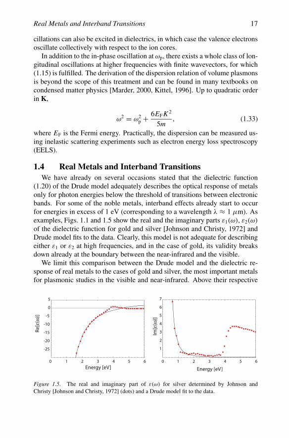
1.4 Real Metals and Interband TransitionsWe have already on several occasions stated that the dielectric function
(1.20) of the Drude model adequately describes the optical response of metalsonly for photon energies below the threshold of transitions between electronicbands. For some of the noble metals, interband effects already start to occurfor energies in excess of 1 eV (corresponding to a wavelength λ ≈ 1 μm). Asexamples, Figs. 1.1 and 1.5 show the real and the imaginary parts ε1(ω), ε2(ω)
of the dielectric function for gold and silver [Johnson and Christy, 1972] andDrude model fits to the data. Clearly, this model is not adequate for describingeither ε1 or ε2 at high frequencies, and in the case of gold, its validity breaksdown already at the boundary between the near-infrared and the visible.
We limit this comparison between the Drude model and the dielectric re-sponse of real metals to the cases of gold and silver, the most important metalsfor plasmonic studies in the visible and near-infrared. Above their respective
1 2 3 4 5 6
-25
-20
-15
-10
-5
0
5
1 2 3 4 5 6
1
2
3
4
5
6
7
Energy [eV] Energy [eV]
Re[ε
(ω)]
Im[ε
(ω)]
0 0
Figure 1.5. The real and imaginary part of ε(ω) for silver determined by Johnson andChristy [Johnson and Christy, 1972] (dots) and a Drude model fit to the data.

18 Electromagnetics of Metals
band edge thresholds, photons are very efficient in inducing interband tran-sitions, where electrons from the filled band below the Fermi surface are ex-cited to higher bands. Theoretically, these can be described using the same ap-proach used for direct band transitions in semiconductors [Ashcroft and Mer-min, 1976, Marder, 2000], and we will not embark on a more detailed discus-sion. The main consequence of these processes concerning surface plasmonpolaritons is an increased damping and competition between the two excita-tions at visible frequencies.
For practical purposes, a big advantage of the Drude model is that it caneasily be incorporated into time-domain based numerical solvers for Maxwell’sequations, such as the finite-difference time-domain (FDTD) scheme [Kashiwaand Fukai, 1990], via the direct calculation of the induced currents using (1.16).Its inadequacy in describing the optical properties of gold and silver at visiblefrequencies can be overcome by replacing (1.16) by
mx + mγ x + mω20x = −eE. (1.34)
Interband transitions are thus described using the classical picture of a boundelectron with resonance frequency ω0, and (1.34) can then be used to calculatethe resulting polarization. We note that a number of equations of this formmight have to be solved (each resulting in a separate contribution to the totalpolarization) in order to model ε(ω) for noble metals accurately. Each of theseequations leads to a Lorentz-oscillator term of the form Ai
ω2i −ω2−iγiω
added to
the free-electron result (1.20) [Vial et al., 2005].
1.5 The Energy of the Electromagnetic Field in MetalsWe finish this chapter by taking a brief look at the energy of the electro-
magnetic field inside metals, or more generally inside dispersive media. Sincethe amount of field localization is often quantified in terms of the electromag-netic energy distribution, a careful consideration of the effects of dispersion isnecessary. For a linear medium with no dispersion or losses (i.e. (1.5) holds),the total energy density of the electromagnetic field can be written as [Jackson,1999]
u = 1
2(E · D + B · H). (1.35)
This expression enters together with the Poynting vector of energy flow S =E × H into the conservation law
∂u
∂t+ ∇ · S = −J · E, (1.36)
relating changes in electromagnetic energy density to energy flow and absorp-tion inside the material.

The Energy of the Electromagnetic Field in Metals 19
In the following, we will concentrate on the contribution uE of the electricfield E to the total electromagnetic energy density. In metals, ε is complex andfrequency-dependent due to dispersion, and (1.35) does not apply. For a fieldconsisting of monochromatic components, Landau and Lifshitz have shownthat the conservation law (1.36) can be held up if uE is replaced by an effectiveelectric energy density ueff, defined as
ueff = 1
2Re
[d(ωε)
dω
]ω0
〈E(r, t) · E(r, t)〉 , (1.37)
where 〈E(r, t) · E(r, t)〉 signifies field-averaging over one optical cycle, andω0 is the frequency of interest. This expression is valid if E is only apprecia-ble in a narrow frequency range around ω0, and the fields are slowly-varyingcompared to a timescale 1/ω0. Furthermore, it is assumed that |ε2| � |ε1|,so that absorption is small. We note that additional care must be taken withthe correct calculation of absorption on the right side of (1.36), where J · Eshould be replaced by ω0Im [ε(ω0)] 〈E(r, t) · E(r, t)〉 if the dielectric responseof the metal is completely described via ε(ω) [Jackson, 1999], in line with thediscussion surrounding (1.10).
The requirement of low absorption limits (1.37) to visible and near-infraredfrequencies, but not to lower frequencies or the regime of interband effectswhere |ε2| > |ε1|. However, the electric field energy can also be determined bytaking the electric polarization explicitly into account, in the form described by(1.16) [Loudon, 1970, Ruppin, 2002]. The obtained expression for the electricfield energy of a material described by a free-electron-type dielectric functionε = ε1 + iε2 of the form (1.20) is
ueff = ε0
4
(ε1 + 2ωε2
γ
)|E|2 , (1.38)
where an additional factor 1/2 is included due to an implicit assumption ofharmonic time dependence of the oscillating fields. For negligible ε2, it can beshown that (1.38) reduces as expected to (1.37) for time-harmonic fields. Wewill use (1.38) in chapter 2 when discussing the amount of energy localizationin fields localized at metallic surfaces.

Chapter 2
SURFACE PLASMON POLARITONS AT METAL /INSULATOR INTERFACES
Surface plasmon polaritons are electromagnetic excitations propagating atthe interface between a dielectric and a conductor, evanescently confined inthe perpendicular direction. These electromagnetic surface waves arise viathe coupling of the electromagnetic fields to oscillations of the conductor’selectron plasma. Taking the wave equation as a starting point, this chapterdescribes the fundamentals of surface plasmon polaritons both at single, flatinterfaces and in metal/dielectric multilayer structures. The surface excitationsare characterized in terms of their dispersion and spatial profile, together witha detailed discussion of the quantification of field confinement. Applicationsof surface plasmon polaritons in waveguiding will be deferred to chapter 7.
2.1 The Wave EquationIn order to investigate the physical properties of surface plasmon polaritons
(SPPs), we have to apply Maxwell’s equations (1.1) to the flat interface be-tween a conductor and a dielectric. To present this discussion most clearly, itis advantageous to cast the equations first in a general form applicable to theguiding of electromagnetic waves, the wave equation.
As we have seen in chapter 1, in the absence of external charge and currentdensities, the curl equations (1.1c, 1.1d) can be combined to yield
∇ × ∇ × E = −μ0∂2D∂t2
. (2.1)
Using the identities ∇ × ∇ × E ≡ ∇(∇ · E) − ∇2E as well as ∇ · (εE) ≡E · ∇ε + ε∇ · E, and remembering that due to the absence of external stimuli∇ · D = 0, (2.1) can be rewritten as

22 Surface Plasmon Polaritons at Metal / Insulator Interfaces
∇(
−1
εE · ∇ε
)− ∇2E = −μ0ε0ε
∂2E∂t2
. (2.2)
For negligible variation of the dielectric profile ε = ε(r) over distances onthe order of one optical wavelength, (2.2) simplifies to the central equation ofelectromagnetic wave theory,
∇2E − ε
c2
∂2E∂t2
= 0. (2.3)
Practically, this equation has to be solved separately in regions of constant ε,and the obtained solutions have to been matched using appropriate boundaryconditions. To cast (2.3) in a form suitable for the description of confinedpropagating waves, we proceed in two steps. First, we assume in all generalitya harmonic time dependence E(r, t) = E(r)e−iωt of the electric field. Insertedinto (2.3), this yields
∇2E + k20εE = 0, (2.4)
where k0 = ωc
is the wave vector of the propagating wave in vacuum. Equation(2.4) is known as the Helmholtz equation.
Next, we have to define the propagation geometry. We assume for sim-plicity a one-dimensional problem, i.e. ε depends only on one spatial coor-dinate. Specifically, the waves propagate along the x-direction of a cartesiancoordinate system, and show no spatial variation in the perpendicular, in-planey-direction (see Fig. 2.1); therefore ε = ε(z). Applied to electromagneticsurface problems, the plane z = 0 coincides with the interface sustaining the
x (direction of propagation)
y
z
Figure 2.1. Definition of a planar waveguide geometry. The waves propagate along the x-direction in a cartesian coordinate system.

The Wave Equation 23
propagating waves,which can now be described as E(x, y, z) = E(z)eiβx . Thecomplex parameter β = kx is called the propagation constant of the travelingwaves and corresponds to the component of the wave vector in the direction ofpropagation. Inserting this expression into (2.4) yields the desired form of thewave equation
∂2E(z)
∂z2+ (
k20ε − β2
)E = 0. (2.5)
Naturally, a similar equation exists for the magnetic field H.Equation (2.5) is the starting point for the general analysis of guided elec-
tromagnetic modes in waveguides, and an extended discussion of its propertiesand applications can be found in [Yariv, 1997] and similar treatments of pho-tonics and optoelectronics. In order to use the wave equation for determiningthe spatial field profile and dispersion of propagating waves, we now need tofind explicit expressions for the different field components of E and H. Thiscan be achieved in a straightforward way using the curl equations (1.1c, 1.1d).
For harmonic time dependence(
∂∂t
= −iω), we arrive at the following set
of coupled equations
∂Ez
∂y− ∂Ey
∂z= iωμ0Hx (2.6a)
∂Ex
∂z− ∂Ez
∂x= iωμ0Hy (2.6b)
∂Ey
∂x− ∂Ex
∂y= iωμ0Hz (2.6c)
∂Hz
∂y− ∂Hy
∂z= −iωε0εEx (2.6d)
∂Hx
∂z− ∂Hz
∂x= −iωε0εEy (2.6e)
∂Hy
∂x− ∂Hx
∂y= −iωε0εEz. (2.6f)
For propagation along the x-direction(
∂∂x
= iβ)
and homogeneity in the y-
direction(
∂∂y
= 0)
, this system of equation simplifies to

24 Surface Plasmon Polaritons at Metal / Insulator Interfaces
∂Ey
∂z= −iωμ0Hx (2.7a)
∂Ex
∂z− iβEz = iωμ0Hy (2.7b)
iβEy = iωμ0Hz (2.7c)∂Hy
∂z= iωε0εEx (2.7d)
∂Hx
∂z− iβHz = −iωε0εEy (2.7e)
iβHy = −iωε0εEz. (2.7f)
It can easily be shown that this system allows two sets of self-consistentsolutions with different polarization properties of the propagating waves. Thefirst set are the transverse magnetic (TM or p) modes, where only the fieldcomponents Ex , Ez and Hy are nonzero, and the second set the transverseelectric (TE or s) modes, with only Hx , Hz and Ey being nonzero.
For TM modes, the system of governing equations (2.7) reduces to
Ex = −i1
ωε0ε
∂Hy
∂z(2.8a)
Ez = − β
ωε0εHy, (2.8b)
and the wave equation for TM modes is
∂2Hy
∂z2+ (
k20ε − β2
)Hy = 0. (2.8c)
For TE modes the analogous set is
Hx = i1
ωμ0
∂Ey
∂z(2.9a)
Hz = β
ωμ0Ey, (2.9b)
with the TE wave equation
∂2Ey
∂z2+ (
k20ε − β2
)Ey = 0. (2.9c)
With these equations at our disposal, we are now in a position to embark onthe description of surface plasmon polaritons.

Surface Plasmon Polaritons at a Single Interface 25
2.2 Surface Plasmon Polaritons at a Single InterfaceThe most simple geometry sustaining SPPs is that of a single, flat interface
(Fig. 2.2) between a dielectric, non-absorbing half space (z > 0) with positivereal dielectric constant ε2 and an adjacent conducting half space (z < 0) de-scribed via a dielectric function ε1(ω). The requirement of metallic characterimplies that Re [ε1] < 0. As shown in chapter 1, for metals this condition isfulfilled at frequencies below the bulk plasmon frequency ωp. We want to lookfor propagating wave solutions confined to the interface, i.e. with evanescentdecay in the perpendicular z-direction.
Let us first look at TM solutions. Using the equation set (2.8) in both halfspaces yields
Hy(z) = A2eiβxe−k2z (2.10a)
Ex(z) = iA21
ωε0ε2k2e
iβxe−k2z (2.10b)
Ez(z) = −A1β
ωε0ε2eiβxe−k2z (2.10c)
for z > 0 and
Hy(z) = A1eiβxek1z (2.11a)
Ex(z) = −iA11
ωε0ε1k1e
iβxek1z (2.11b)
Ez(z) = −A1β
ωε0ε1eiβxek1z (2.11c)
for z < 0. ki ≡ kz,i(i = 1, 2) is the component of the wave vector perpen-dicular to the interface in the two media. Its reciprocal value, z = 1/ |kz|,defines the evanescent decay length of the fields perpendicular to the interface,
Metal
Dielectricx
z
Figure 2.2. Geometry for SPP propagation at a single interface between a metal and a dielec-tric.

26 Surface Plasmon Polaritons at Metal / Insulator Interfaces
which quantifies the confinement of the wave. Continuity of Hy and εiEz atthe interface requires that A1 = A2 and
k2
k1= −ε2
ε1. (2.12)
Note that with our convention of the signs in the exponents in (2.10,2.11),confinement to the surface demands Re [ε1] < 0 if ε2 > 0 - the surface wavesexist only at interfaces between materials with opposite signs of the real partof their dielectric permittivities, i.e. between a conductor and an insulator. Theexpression for Hy further has to fulfill the wave equation (2.8c), yielding
k21 = β2 − k2
0ε1 (2.13a)
k22 = β2 − k2
0ε2. (2.13b)
Combining this and (2.12) we arrive at the central result of this section, thedispersion relation of SPPs propagating at the interface between the two halfspaces
β = k0
√ε1ε2
ε1 + ε2. (2.14)
This expression is valid for both real and complex ε1, i.e. for conductors with-out and with attenuation.
Before discussing the properties of the dispersion relation (2.14) in moredetail, we now briefly analyze the possibility of TE surface modes. Using(2.9), the respective expressions for the field components are
Ey(z) = A2eiβxe−k2z (2.15a)
Hx(z) = −iA21
ωμ0k2e
iβxe−k2z (2.15b)
Hz(z) = A2β
ωμ0eiβxe−k2z (2.15c)
for z > 0 and
Ey(z) = A1eiβxek1z (2.16a)
Hx(z) = iA11
ωμ0k1e
iβxek1z (2.16b)
Hz(z) = A1β
ωμ0eiβxek1z (2.16c)

Surface Plasmon Polaritons at a Single Interface 27
Wave vector βc/ωp
Freq
uen
cy ω
/ωp
1
1
0.2
0.4
0.6
0.8
air silica
00
ωsp,air
ωsp,silica
Figure 2.3. Dispersion relation of SPPs at the interface between a Drude metal with negligiblecollision frequency and air (gray curves) and silica (black curves).
for z < 0. Continuity of Ey and Hx at the interface leads to the condition
A1 (k1 + k2) = 0. (2.17)
Since confinement to the surface requires Re [k1] > 0 and Re [k2] > 0, thiscondition is only fulfilled if A1 = 0, so that also A2 = A1 = 0. Thus, nosurface modes exist for TE polarization. Surface plasmon polaritons only existfor TM polarization.
We now want to examine the properties of SPPs by taking a closer look attheir dispersion relation. Fig. 2.3 shows plots of (2.14) for a metal with negli-gible damping described by the real Drude dielectric function (1.22) for an air(ε2 = 1) and a fused silica (ε2 = 2.25) interface. In this plot, the frequency ω isnormalized to the plasma frequency ωp, and both the real (continuous curves)and the imaginary part (broken curves) of the wave vector β are shown. Dueto their bound nature, the SPP excitations correspond to the part of the dis-persion curves lying to the right of the respective light lines of air and silica.Thus, special phase-matching techniques such as grating or prism coupling arerequired for their excitation via three-dimensional beams, which will be dis-cussed in chapter 3. Radiation into the metal occurs in the transparency regimeω > ωp as mentioned in chapter 1. Between the regime of the bound andradiative modes, a frequency gap region with purely imaginary β prohibitingpropagation exists.
For small wave vectors corresponding to low (mid-infrared or lower) fre-quencies, the SPP propagation constant is close to k0 at the light line, and the

28 Surface Plasmon Polaritons at Metal / Insulator Interfaces
waves extend over many wavelengths into the dielectric space. In this regime,SPPs therefore acquire the nature of a grazing-incidence light field, and arealso known as Sommerfeld-Zenneck waves [Goubau, 1950].
In the opposite regime of large wave vectors, the frequency of the SPPsapproaches the characteristic surface plasmon frequency
ωsp = ωp√1 + ε2
, (2.18)
as can be shown by inserting the free-electron dielectric function (1.20) into(2.14). In the limit of negligible damping of the conduction electron oscillation(implying Im [ε1(ω)] = 0), the wave vector β goes to infinity as the frequencyapproaches ωsp, and the group velocity vg → 0. The mode thus acquireselectrostatic character, and is known as the surface plasmon. It can indeed beobtained via a straightforward solution of the Laplace equation ∇2φ = 0 forthe single interface geometry of Fig. 2.2, where φ is the electric potential. Asolution that is wavelike in the x-direction and exponentially decaying in thez-direction is given by
φ(z) = A2eiβxe−k2z (2.19)
for z > 0 and
φ(z) = A1eiβxek1z (2.20)
for z < 0. ∇2φ = 0 requires that k1 = k2 = β: the exponential decaylengths
∣∣z∣∣ = 1/kz into the dielectric and into the metal are equal. Continuityof φ and ε∂φ/∂z ensure continuity of the tangential field components and thenormal components of the dielectric displacement and require that A1 = A2
and additionally
ε1(ω) + ε2 = 0. (2.21)
For a metal described by a dielectric function of the form (1.22), this condi-tion is fulfilled at ωsp. Comparison of (2.21) and (2.14) show that the surfaceplasmon is indeed the limiting form of a SPP as β → ∞.
The above discussions of Fig. 2.3 have assumed an ideal conductor withIm [ε1] = 0. Excitations of the conduction electrons of real metals howeversuffer both from free-electron and interband damping. Therefore, ε1(ω) iscomplex, and with it also the SPP propagation constant β. The traveling SPPsare damped with an energy attenuation length (also called propagation length)L = (2Im
[β])−1, typically between 10 and 100 μm in the visible regime,
depending upon the metal/dielectric configuration in question.Fig. 2.4 shows as an example the dispersion relation of SPPs propagating at
a silver/air and silver/silica interface, with the dielectric function ε1(ω) of silver

Surface Plasmon Polaritons at a Single Interface 29
Wave vector Re{β }[107 m-1]
Freq
uen
cy ω
[101
5 H
z]
2
4
6
8
10
00 2 4 6 8
air silica
Figure 2.4. Dispersion relation of SPPs at a silver/air (gray curve) and silver/silica (blackcurve) interface. Due to the damping, the wave vector of the bound SPPs approaches a finitelimit at the surface plasmon frequency.
taken from the data obtained by Johnson and Christy [Johnson and Christy,1972]. Compared with the dispersion relation of completely undamped SPPsdepicted in Fig. 2.3, it can be seen that the bound SPPs approach now a maxi-mum, finite wave vector at the the surface plasmon frequency ωsp of the system.This limitation puts a lower bound both on the wavelength λsp = 2π/Re
[β]
of the surface plasmon and also on the amount of mode confinement perpen-dicular to the interface, since the SPP fields in the dielectric fall off as e−|kz||z|
with kz =√
β2 − ε2(
ωc
)2. Also, the quasibound, leaky part of the dispersion
relation between ωsp and ωp is now allowed, in contrast to the case of an idealconductor, where Re
[β] = 0 in this regime (Fig. 2.3).
We finish this section by providing an example of the propagation length L
and the energy confinement (quantified by z) in the dielectric. As is evidentfrom the dispersion relation, both show a strong dependence on frequency.SPPs at frequencies close to ωsp exhibit large field confinement to the inter-face and a subsequent small propagation distance due to increased damping.Using the theoretical treatment outlined above, we see that SPPs at a silver/airinterface at λ0 = 450 nm for example have L ≈ 16 μm and z ≈ 180 nm.At λ0 ≈ 1.5 μm however, L ≈ 1080 μm and z ≈ 2.6 μm. The better theconfinement, the lower the propagation length. This characteristic trade-offbetween localization and loss is typical for plasmonics. We note that field-confinement below the diffraction limit of half the wavelength in the dielectriccan be achieved close to ωsp. In the metal itself, the fields fall off over distances

30 Surface Plasmon Polaritons at Metal / Insulator Interfaces
on the order of 20 nm over a wide frequency range spanning from the visibleto the infrared.
2.3 Multilayer SystemsWe now turn our attention to SPPs in multilayers consisting of alternating
conducting and dielectric thin films. In such a system, each single interfacecan sustain bound SPPs. When the separation between adjacent interfaces iscomparable to or smaller than the decay length z of the interface mode, in-teractions between SPPs give rise to coupled modes. In order to elucidatethe general properties of coupled SPPs, we will focus on two specific three-layer systems of the geometry depicted in Fig. 2.5: Firstly, a thin metalliclayer (I) sandwiched between two (infinitely) thick dielectric claddings (II,III), an insulator/metal/insulator (IMI) heterostructure, and secondly a thin di-electric core layer (I) sandwiched between two metallic claddings (II, III), ametal/insulator/metal (MIM) heterostructure.
Since we are here only interested in the lowest-order bound modes, westart with a general description of TM modes that are non-oscillatory in thez-direction normal to the interfaces using (2.8). For z > a, the field compo-nents are
Hy = Aeiβxe−k3z (2.22a)
Ex = iA1
ωε0ε3k3eiβxe−k3z (2.22b)
Ez = −Aβ
ωε0ε3eiβxe−k3z, (2.22c)
while for z < −a we get
x
z
a
-a
III
I
II
Figure 2.5. Geometry of a three-layer system consisting of a thin layer I sandwiched betweentwo infinite half spaces II and III.

Multilayer Systems 31
Hy = Beiβxek2z (2.23a)
Ex = −iB1
ωε0ε2k2eiβxek2z (2.23b)
Ez = −Bβ
ωε0ε2eiβxek2z. (2.23c)
Thus, we demand that the fields decay exponentially in the claddings (II) and(III). Note that for simplicity as before we denote the component of the wavevector perpendicular to the interfaces simply as ki ≡ kz,i .
In the core region −a < z < a, the modes localized at the bottom and topinterface couple, yielding
Hy = Ceiβxek1z + Deiβxe−k1z (2.24a)
Ex = −iC1
ωε0ε1k1eiβxek1z + iD
1
ωε0ε1k1eiβxe−k1z (2.24b)
Ez = Cβ
ωε0ε1eiβxek1z + D
β
ωε0ε1eiβxe−k1z. (2.24c)
The requirement of continutity of Hy and Ex leads to
Ae−k3a = Cek1a + De−k1a (2.25a)A
ε3k3e−k3a = −C
ε1k1ek1a + D
ε1k1e−k1a (2.25b)
at z = a and
Be−k2a = Ce−k1a + Dek1a (2.26a)
−B
ε2k2e−k2a = −C
ε1k1e−k1a + D
ε1k1ek1a (2.26b)
at z = −a, a linear system of four coupled equations. Hy further has to fulfillthe wave equation (2.8c) in the three distinct regions, via
k2i = β2 − k2
0εi (2.27)
for i = 1, 2, 3. Solving this system of linear equations results in an implicitexpression for the dispersion relation linking β and ω via
e−4k1a = k1/ε1 + k2/ε2
k1/ε1 − k2/ε2
k1/ε1 + k3/ε3
k1/ε1 − k3/ε3. (2.28)

32 Surface Plasmon Polaritons at Metal / Insulator Interfaces
We note that for infinite thickness (a → ∞), (2.28) reduces to (2.12), theequation of two uncoupled SPP at the respective interfaces.
We will from this point onwards consider the interesting special case wherethe sub- and the superstrates (II) and (III) are equal in terms of their dielectricresponse, i.e. ε2 = ε3 and thus k2 = k3. In this case, the dispersion relation(2.28) can be split into a pair of equations, namely
tanh k1a = −k2ε1
k1ε2(2.29a)
tanh k1a = −k1ε2
k2ε1. (2.29b)
It can be shown that equation (2.29a) describes modes of odd vector parity(Ex(z) is odd, Hy(z) and Ez(z) are even functions), while (2.29b) describesmodes of even vector parity (Ex(z) is even function, Hy(z) and Ez(z) are odd).
The dispersion relations (2.29a, 2.29b) can now be applied to IMI and MIMstructures to investigate the properties of the coupled SPP modes in these twosystems. We first start with the IMI geometry - a thin metallic film of thick-ness 2a sandwiched between two insulating layers. In this case ε1 = ε1(ω)
represents the dielectric function of the metal, and ε2 the positive, real dielec-tric constant of the insulating sub- and superstrates. As an example, Fig. 2.6shows the dispersion relations of the odd and even modes (2.29a, 2.29b) for anair/silver/air geometry for two different thicknesses of the silver thin film. For
2 4 6 8
2
4
6
8
Wave vector β [107 m-1]0
Freq
uen
cy ω
[1015
Hz]
0
odd modes ω+
even modes ω−
Figure 2.6. Dispersion relation of the coupled odd and even modes for an air/silver/air mul-tilayer with a metal core of thickness 100 nm (dashed gray curves) and 50 nm (dashed blackcurves). Also shown is the dispersion of a single silver/air interface (gray curve). Silver ismodeled as a Drude metal with negligible damping.

Multilayer Systems 33
simplicity, here the dielectric function of silver is approximated via a Drudemodel with negligible damping (ε(ω) real and of the form (1.22)), so thatIm
[β] = 0.
As can be seen, the odd modes have frequencies ω+ higher than the respec-tive frequencies for a single interface SPP, and the even modes lower frequen-cies ω−. For large wave vectors β (which are only achievable if Im [ε(ω)] = 0),the limiting frequencies are
ω+ = ωp√1 + ε2
√1 + 2ε2e−2βa
1 + ε2(2.30a)
ω− = ωp√1 + ε2
√1 − 2ε2e−2βa
1 + ε2. (2.30b)
Odd modes have the interesting property that upon decreasing metal filmthickness, the confinement of the coupled SPP to the metal film decreases asthe mode evolves into a plane wave supported by the homogeneous dielectricenvironment. For real, absorptive metals described via a complex ε(ω), thisimplies a drastically increased SPP propagation length [Sarid, 1981]. Theselong-ranging SPPs will be further discussed in chapter 7. The even modesexhibit the opposite behavior - their confinement to the metal increases withdecreasing metal film thickness, resulting in a reduction in propagation length.
Moving on to MIM geometries, we now set ε2 = ε2(ω) as the dielectricfunction of the metal and ε1 as the dielectric constant of the insulating corein equations (2.29a, 2.29b). From an energy confinement point of view, themost interesting mode is the fundamental odd mode of the system, which doesnot exhibit a cut-off for vanishing core layer thickness [Prade et al., 1991].Fig. 2.7 shows the dispersion relation of this mode for a silver/air/silver het-erostructure. This time, the dielectric function ε(ω) was taken as a complex fitto the dielectric data of silver obtained by Johnson and Christy [Johnson andChristy, 1972]. Thus β does not go to infinity as the surface plasmon frequencyis approached, but folds back and eventually crosses the light line, as for SPPspropagating at single interfaces.
It is apparent that large propagation constants β can be achieved even forexcitation well below ωsp, provided that the width of the dielectric core is cho-sen sufficiently small. The ability to access such large wave vectors and thussmall penetration lengths z into the metallic layers by adjusting the geometryindicates that localization effects that for a single interface can only be sus-tained at excitations near ωsp, can for such MIM structures also be attained forexcitation out in the the infrared. An analysis of various other MIM structures,for example concentric shells, has given similar results [Takahara et al., 1997].Geometries amendable to easy fabrication such as triangular metal V-grooves

34 Surface Plasmon Polaritons at Metal / Insulator Interfaces
Wave vector Re{β}[107 m-1]0 2 4 6 8
Freq
uen
cy ω
[101
5 H
z]
2
4
6
0
2a
air AgAg
x
z
|Ez|
Figure 2.7. Dispersion relation of the fundamental coupled SPP modes of a silver/air/silvermultilayer geometry for an air core of size 100 nm (broken gray curve), 50 nm (broken blackcurve), and 25 nm (continuous black curve). Also shown is the dispersion of a SPP at a singlesilver/air interface (gray curve) and the air light line (gray line).
on a flat metal surface have already shown great promise for applications inwaveguiding, which will be presented in chapter 7.
We have limited our discussion of coupled SPPs in three-layer structuresto the fundamental bound modes of the system, with a view on applicationsin waveguiding and confinement of electromagnetic energy. It is important tonote that the family of modes supported by this geometry is much richer thandescribed in this treatment. For example, for IMI structures, we have omitted adiscussion of leaky modes, and MIM layers can also exhibit oscillatory modesfor sufficient thickness of the dielectric core. Additionally, the coupling be-tween SPPs at the two core/cladding interfaces changes significantly when thedielectric constants of the sub- and superstrates are different, so that ε2 �= ε3,prohibiting phase-matching between the modes located at the two interfaces.A detailed treatment of these cases can be found in [Economou, 1969, Burkeand Stegeman, 1986, Prade et al., 1991].
2.4 Energy Confinement and the Effective Mode LengthIn chapter 5 we will see that using localized surface plasmons in metal
nanoparticles, electromagnetic energy can be confined or squeezed into vol-umes smaller than the diffraction limit (λ0/2n)3, where n = √
ε is the re-fractive index of the surrounding medium. This high confinement leads to aconcomitant field enhancement and is of prime importance in plasmonics, en-abling a great variety of applications in optical sensing, as will be discussedin chapter 9. In the essentially one-dimensional cases of single interfaces and

Energy Confinement and the Effective Mode Length 35
0.01
0.1
1
10
10-2 110-4
normalized gap size
% e
ner
gy
in m
etal
0.1
1
Gap size 2a [nm]20 8010
β/k 0
2
Mo
de
Len
gth
, L ef
f
10-1
_
10-2
10-3
10-4
(c)
(b)(a) 100
10-3 10-1 10
1
10
10-2 110-4
normalized gap size10-3 10-1 10
Figure 2.8. Energy confinement in a gold/air/gold MIM structure. (a) Real (solid curve) andimaginary (dashed curve) part of the normalized propagation constant β versus gap size atλ0 = 850nm. (b) Fraction of electric field energy residing inside the metallic half spaces asa function of normalized gap size for excitation at λ0 = 600 nm (thick curve), 850nm (blackcurve), 1.5 μm (gray curve), 10 μm (broken black curve), and 100 μm (broken gray curve). (c)Effective mode length Leff normalized to free-space wavelength λ0 as a function of gap size.Adapted from [Maier, 2006b].
multilayer structures presented above that support propagating SPPs, energylocalization below the diffraction limit perpendicular to the interface(s) is alsopossible. We have already hinted at this phenomenon when stating that the fielddecay length z in the dielectric layers can be significantly smaller than λ0/n.
However, care must be taken when quantifying energy confinement, sincea sub-wavelength field decay length z on the dielectric side of the interfaceimplies that a significant amount of the total electric field energy of the SPPmode resides inside the metal. This energy must be taken into account using(1.38) when calculating the spatial distribution of the electric energy density,since for the quantification of the strength of interactions between light andmatter (e.g. a molecule placed into the field), the field strength per unit energy(i.e., single photon) is of importance.
Taking a gold/air/gold MIM heterostructure as an example, Fig. 2.8(a) showsthe evolution of both the real and imaginary parts of the propagation constantβ of the fundamental SPP mode with varying gap size for excitation at a freespace wavelength of λ0 = 850 nm, calculated using Drude fits to the dielectric

36 Surface Plasmon Polaritons at Metal / Insulator Interfaces
function of gold [Johnson and Christy, 1972, Ordal et al., 1983]. Both partsincrease with decreasing gap size, since the mode is becoming more electron-plasma in character, suggesting that the electromagnetic energy is residing in-creasingly in the metal half-spaces. A plot of the fractional amount of theelectric field energy inside the metal regions is shown in Fig. 2.8(b) for exci-tation at wavelengths λ0 = 600 nm, 850 nm, 1.5 μm, 10 μm, and 100 μm(= 3 THz). For a gap of 20 nm for example, at λ0 = 850 nm this fraction al-ready reaches 40%. Note that the gap size is normalized to the respective freespace wavelength. It is apparent that along with the increased localization ofthe field to the gold/air interface, either via small gap sizes or excitation closerto ωsp, comes a shift of the energy into the metal regions.
In order to get a better handle on the consequences of increasing fractionsof the total energy of the mode entering the metallic cladding upon decreasingsize of the dielectric gap, we can define in analogy to the effective mode volumeVeff used to quantify the strength of light-matter interactions in cavity quantumelectrodynamics [Andreani et al., 1999] an effective mode length Leff, with
Leff(z0)ueff(z0) =∫
ueff(z)dz. (2.31)
ueff(z0) represents the electric field energy density at a position z0 of interestwithin the air core (e.g. the location of an emitter). In this one-dimensionalpicture, the effective mode length is therefore given as the ratio of the totalenergy of the SPP mode divided by the energy density (energy per unit length)at the position of interest, which is often taken as the position of highest field.In a quantized picture for normalized total energy, the inverse of the effectivemode length thus quantifies the field strength per single SPP excitation. Moredetails can be found in [Maier, 2006b].
A determination of the effective mode length of MIM structures allows anexamination how the electric field strength per SPP excitation in the air gapscales as a function of the gap size. Fig. 2.8(c) shows the variation of Leff
(normalized to the free-space wavelength λ0) with normalized gap size. z0 istaken to be at the air side of the air/gold boundary, where the electric fieldstrength is maximum. The mode lengths drop well below λ0/2, demonstratingthat plasmonic metal structures can indeed sustain effective as well as physicalmode lengths below the diffraction limit of light. The trend in Leff with gap sizetends to scale with the physical extent of the air gap. For large normalized gapsizes and low frequencies, this is due to the delocalized nature of the surfaceplasmon, leading to smaller mode lengths for excitation closer to the surfaceplasmon frequency ωsp for the same normalized gap size.
As the gap size is reduced to a point where the dispersion curve of the SPPmode turns over (see Fig. 2.7) and energy begins to enter the metallic halfspaces, the continued reduction in mode length is due to an increase in field

Energy Confinement and the Effective Mode Length 37
localization to the metal-air interface. In this regime, excitations with lowerfrequencies show smaller mode lengths for the same normalized gap size thanexcitations closer to the plasmon resonance, due to the fact that more energyresides inside the metal for the latter. We note that for very small gaps with2a < 2 nm, the effects of local fields due to unscreened surface electronsbecome important [Larkin et al., 2004], leading to a further decrease in Leff.This cannot be captured using the dielectric function approach.
To summarize, we see that despite the penetration of a significant amountof energy of a SPP mode into the conducting medium (for excitation near ωsp
or in small gap structures), the associated large propagation constants β ensurethat the effective extent of the mode perpendicular to the interface(s) dropswell below the diffraction limit.