electro-chemical migration idea stage project wallace ables - dell hdp user group member meeting...
TRANSCRIPT

Electro-Chemical Migration
Idea Stage Project Wallace Ables - Dell
HDP User Group Member MeetingHost: Multek
Boeblingen, Germany
May 22, 2012
Phone-in Presentation
© HDP User Group International, Inc.
2
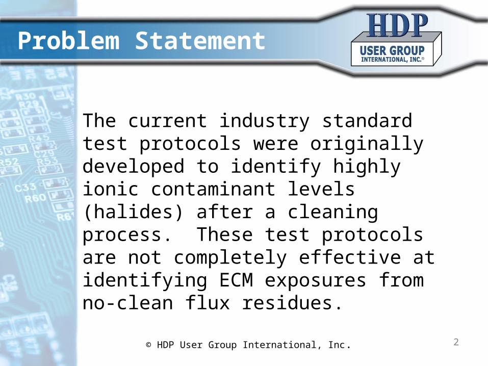
Problem Statement
The current industry standard test protocols were originally developed to identify highly ionic contaminant levels (halides) after a cleaning process. These test protocols are not completely effective at identifying ECM exposures from no-clean flux residues.
© HDP User Group International, Inc.

3
Background
1. Various forms of corrosion and Electro Chemical Migration failures on products that pass the current cleanliness and corrosion resistance test protocols have demonstrated that these test procedures are not effective.
2. The failure mechanism is the same regardless what segment of the electronics industry the PCBA is used.
3. The current testing does not take into consideration various acceleration factors associated with no clean flux and product design features.
© HDP User Group International, Inc

4
No clean ECM corrosion failures
Surface corrosion
Solder mask Porosity
Open trace / solder mask opening
Open trace / solder mask
opening
Surface corrosion
Dendrite / short / open
Dendrite / short
Dendrite / short
© HDP User Group International, Inc.

5
Project Objectives
Identify required enhancements to the current industry specifications, test methods, and coupon design to mitigate the electro-chemical migration and corrosion induced failures when no clean flux systems are used.
Cleanliness testing Corrosion resistance testing ECM testing Maximum acceptable residue levels by class of
product Minimum acceptable solder mask properties Product design recommendations
© HDP User Group International, Inc.

Not in immediate scope
6
Some closely aligned aspects of this project will be put off until a follow-on project is underway. Therefore the following issues will not be in the scope of this project:
1. Conformal coating over no-clean fluxes. This may allow ECM under the conformal coating.
2. Solder mask test standards for ECM controls.
© HDP User Group International, Inc

7
Project Goals
1. Develop a set of specifications and test methods (or enhancements to the current industry specifications) for cleanliness testing, corrosion resistance testing, and ECM testing to identify exposures when no clean flux systems are used.a. SMT flux residuesb. Wave solder flux residuesc. Rework flux residues – qualification for flux
application methods, controls, acceptable residue levels, and test methods
d. Develop acceptable flux residue thresholds based on test results
e. Develop different acceptance levels based on product class levels
© HDP User Group International, Inc.

8
Project Goals
2. Identify enhancements to the test methods, test procedures, and test coupon design that take into account significant solder mask properties and product design features that influence the development of ECM and corrosion failures.a. Exposed Cu from solder mask openings (pin
holes, undercut, damage, etc.)b. Moisture and chemical absorption propertiesc. Minimum cure leveld. Voltage bias on a tracee. Minimum spacing between positive and
negative features to prevent ECM
© HDP User Group International, Inc.

Team Members –To Date
• Agilent • Alcatel-Lucent • Arlon • ASE• Cisco• Dell• Ericsson• Flextronics• IBM
• Intel• Isola• Nihon-Superior• Oracle• Phillips• Plexus Plexus • Rockwell • TTM Tech
9© HDP User Group International, Inc.