eindhoven university of technology master efficient ... vhdl and netlist level the verification is...
TRANSCRIPT

Eindhoven University of Technology
MASTER
Efficient implementation of a WCDMA RAKE receiver on a programmable platform
Quax, M.M.G.
Award date:2003
DisclaimerThis document contains a student thesis (bachelor's or master's), as authored by a student at Eindhoven University of Technology. Studenttheses are made available in the TU/e repository upon obtaining the required degree. The grade received is not published on the documentas presented in the repository. The required complexity or quality of research of student theses may vary by program, and the requiredminimum study period may vary in duration.
General rightsCopyright and moral rights for the publications made accessible in the public portal are retained by the authors and/or other copyright ownersand it is a condition of accessing publications that users recognise and abide by the legal requirements associated with these rights.
• Users may download and print one copy of any publication from the public portal for the purpose of private study or research. • You may not further distribute the material or use it for any profit-making activity or commercial gain
Take down policyIf you believe that this document breaches copyright please contact us providing details, and we will remove access to the work immediatelyand investigate your claim.
Download date: 17. May. 2018

TUIe technlsche universltelt elndhaven
Faculty of Electrical EngineeringSection Design Technology For Electronic Systems (ICStES)
ICS-ES 821
Master's Thesis
EFFICIENT IPLEMENTATION OF A WCDMARAKE RECEIVER ON A PROGRAMMABLE
PLATFORM
M.M.G. Quax
Supervisor:Date:
prof.dr.ir. J.L. van MeerbergenJune 2003
The Faoulty of Electrical Engineering of the Eindhoven University of Technology does notaooept any responsibility regarding the contents of Master's Theses

13/06n003
Authors' address data: M.M.G. Quax ; [email protected]. J.L. van Meerbergen
©Eindhoven University ofTechnology 2003All rights reserved. Reproduction in whole or in part is
prohibited without the written consent of the copyright owner.
ii ©Eindhoven University of Technology 2003

Master's Thes":
Title:
Author(s):
Section:
Group:
Department:
University:
Keywords:
Abstract:
Conclusions:
13/0612003
13/06/2003
Efficient implementation of a WCDMA RAKE receiveron a programmable platform
M.M.G.Quax
Design Automation Section
Information and Communications Systems Group
Department of Electrical Engineering
Eindhoven University of Technology
WCDMA; RAKE; programmable digital signalprocessor; reconfigurl\ble computing; wireless communication; spread spectrum
TIlls thesis is a study of an efficient programmable implementation of a WCDMARake receiver. The focus has been on doing a scalable implementation withsmall distributed memories and low power consumption. The programmableRake receiver implemented as part of this thesis has been written in AIRT Cand functionally simulated and verified using Matlab / Simulink. At VHDL andnetlist level the verification is done with Cadence ncsim. The area and powerconsumption have been estimated with synthesis (Cadence) and power estimation using a wire load model. In this thesis two system design choices are madeby mapping the Rake algorithm on an A IRT processor template. The first choiceconcerns the placement of the alignment memory. By moving the time alignment of the "fingers" (multipath components) from the beginning of a Rakereceiver into the maximum ratio combiner, we have shown that not only willwe reduce the memory access bandwidth but also the memory area. The secondchoice influences the exploiting of parallelism. By placing branch conditionsnot in the control flow but locally in the data path, the algorithm can fully exploit the parallelism in the algorithm. The resulting architecture consists of amixture of generic functional units, extended functional units (with conditionalinput) and dedicated functional units for bit level operations.
The results of this thesis are power and area numbers of a programmable Rakereceiver:Area: 0.2 mm2 - 0.121i CMOSPower: 6 mW/lOO MHz! 0.2 mm2 I 1.2V
©Eindhoven University of Technology 2003 iii

13/06/2003
PrefaceThis Master thesis was done at the Eindhoven University of Technology, the Netherlands during september2002 and may 2003 as part of my M.Sc Electrical Engineering studies at the Department of ElectricalEngineering, Information and Communications Systems Group at the Eindhoven University of Technology.
Eindhoven, 17th June 2003
iv @Eindhoven University of Technology 2003

13/0612003
Contents
1 Introduction 1
1.1 Background
1.2 Thesis objectives
1.3 Organization of the thesis .
2 WCDMA 2
2.1 Introduction 2
2.2 CDMA basics 2
2.2.1 Direct sequence CDMA 3
2.2.2 Spreading and despreading . 5
2.2.3 Multiple access 7
2.3 Spreading codes . . . . 9
2.3.1 Properties of PN sequences. 9
2.3.2 M-sequence. . .. 9
2.3.3 Scrambling codes . 10
2.3.4 Channelization codes . 11
2.4 Performance in the presence of interference 12
2.4.1 Narrowband interference. 12
2.4.2 Wideband interference .. 12
2.4.3 Multiple access interference 13
2.4.4 Power control . 14
2.5 Multi path ....... 15
2.5.1 Rake receiver . 17
2.5.2 Channel Estimation . 19
2.5.3 Maximum Ratio Combining 20
2.6 Soft and softer hand over 21
2.7 Synchronization . . . . . 23
2.7.1 Acquisition phase (coarse alignment) 23
2.7.2 Tracking phase (fine alignment) 25
3 Rake receiver architecture 26
3.1 Rake? ...... 26
3.2 Rake in literature 26
3.3 Conventional Rake receiver . 28
3.4 FlexRake receiver . . . 29
3.4.1 Stream buffer . 30
3.4.2 correlator engine 30
3.4.3 control ..... 31
3.5 Post buffer Rake receiver, ASIC implementation . 32
©Eindhoven University of Technology 2003 v

13/0612003
3.5.1 Chip Aligner
3.5.2 PN generator
3.5.3 Descrambler
3.5.4 Despreader
3.5.5 OVSF generator
3.5.6 Symboldespreader
3.5.7 Channel compensator.
3.5.8 MRC .........
3.6 R.E.A.L. DSP implementation
3.6.1 Input stage ..
3.6.2 Receiver finger
3.6.3 Delay block . .
3.6.4 Weighting block
3.6.5 Combination block
3.6.6 Rake scheduler .
3.6.7 Implementation .
3.6.8 offset adjustment
3.6.9 Conclusion ...
4 Designftow
4.1 introduction
4.2 Matlab/ Simulink
4.2.1 Associated files .
4.2.2 S-Function
4.3 AIRT Designer ..
4.3.1 Processor architecture template
4.3.2 Logic synthesis
4.4 Behavioral synthesis .
4.4.1 Behavioral Synthesis Concepts.
4.4.2 Behaviorallirnitations
4.5 VHDL / Verilog simulation ..
4.6 Power estimations: DIESEL wire load model
4.6.1 Dissipation in CMOS circuits
4.6.2 Static power dissipation ..
4.6.3 Dynamic power dissipation.
4.6.4 calculating power dissipation.
4.6.5 Wire load models . . . . . . .
4.6.6 Back annotation of wire capacitance .
4.6.7 Back annotation of timing
4.6.8 Test bench dependence ..
vi
32
33
34
34
34
36
37
37
38
38
39
39
40
40
40
40
40
41
42
42
44
44
46
47
49
51
52
52
52
53
54
54
55
55
55
57
58
58
58
©Eindhoven University of Technology 2003

5 Architecture
5.1
5.2
5.3
5.4
5.5
Introduction
System architecture design trade offs .
5.2.1 Scalability of the design
5.2.2 memory usage balance
Exploiting parallelism. . . . .
5.3.1 limitations to parallelism .
5.3.2 Control dependency: Reduce sequential bottlenecks.
5.3.3 Load balance .
processor architecture .
Benchmark .
5.5.1 Operating conditions
5.5.2 Power estimation
5.5.3 Area .
5.5.4 Timing report .
5.5.5 Conclusions ..
13/06/2003
59
59
59
59
61
69
69
70
78
79
80
80
80
81
82
83
References
Index
©Eindhoven University of Technology 2003
84
87
vii
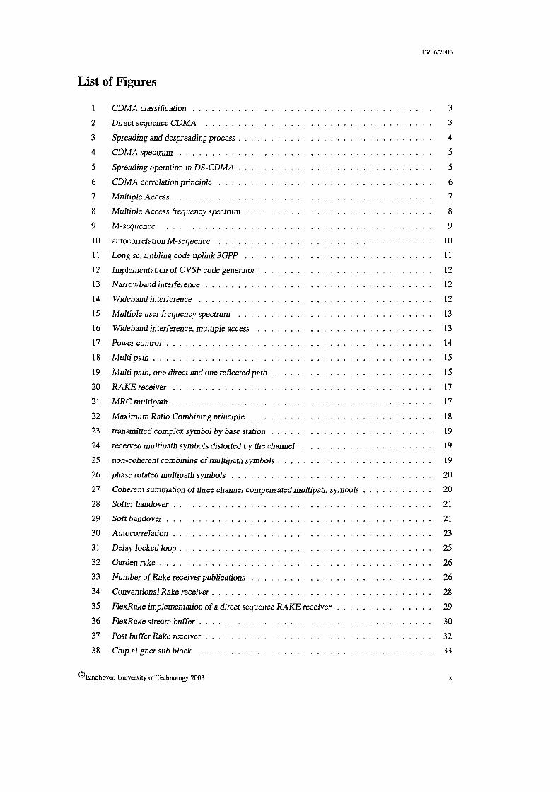
List of Figures
1 CDMA classification
2 Direct sequence CDMA
3 Spreading and despreading process .
4 CDMA spectrum . . . . . . . . .
5 Spreading operation in DS-CDMA
6 CDMA correlation principle
7 Multiple Access . . . . . . .
8 Multiple Access frequency spectrum
9 M-sequence ..
10 autocorrelation M-sequence
11 Long scrambling code uplink 3GPP
12 Implementation of OVSF code generator.
13 Narrowband interference
14 Wideband interference
15 Multiple user frequency spectrum
16 Wideband interference, multiple access
17 Power control
18 Multi path ..
19 Multi path, one direct and one reflected path .
20 RAKE receiver
21 MRC multipath
22 Maximum Ratio Combining principle
23 transmitted complex symbol by base station
24 received multipath symbols distorted by the channel
25 non-coherent combining ofmultipath symbols .
26 phase rotated multipath symbols . . . . . . . .
27 Coherent summation of three channel compensated multipath symbols .
28 Softer handover .
29 Soft handover .
30 Autocorrelation
31 Delay locked loop .
32 Garden rake . ...
33 Number ofRake receiver publications
34 Conventional Rake receiver. . . . . .
35 FlexRake implementation of a direct sequence RAKE receiver
36 FlexRake stream buffer .
37 Post buffer Rake receiver
38 Chip aligner sub block ..
©Eindhoven University of Technology 2003
13/0612003
3
3
4
5
5
6
7
8
9
10
11
12
12
12
13
13
14
15
15
17
17
18
19
19
19
20
20
21
21
23
25
26
26
28
29
30
32
33
ix

©Eindhoven University of Technology 2003
13/0612003
39
40
41
42
43
44
45
46
47
48
49
50
51
52
53
54
55
56
57
58
59
60
61
62
63
64
65
66
67
68
69
70
71
72
73
74
75
76
77
78
x
Chip aligner . . . . . . . . . .
Time multiplexed pn generator
Descrambler .
Despreader .
OVSF generator .
Symboldespreader
Channelization code multiplier
Complex multiplier
VDBmemory .
MRC .....
R.E.A.L. implementation ofRAKE receiver
Timing diagram input stage . .
Block diagram receiver finger
Designflow .
Mathworks Simulink WCDMA FDD model
Simulink sub model ofRake receiver.
Simulink sub model of Rake receiver.
Simulink customized interface
ART designer main gui . .
ART Designer design flow
ART Designer architectural model
ART Designer architectural model from register to register
Timing and functional behavior analysis
Cadence NC VHDL
Power dissipation in a CMOS inverter cell
Currents in a basic CMOS circuit for rising and falling output transitions.
Common memory resource .
Distributed memory resources
Memory alignment before despreading, FlexRake implementation
Single memory, alignment after despreading . .
Distributed memory, alignment after despreading
Memory alignment in Maximum ratio combiner
Memory size vs. rake receivers ...
Memory bandwidth vs. rake receivers
Example of conditional code in Rake algorithm .
General VLIW architecture . . . . . . . . . . .
Serial schedule ofRake algorithm on single thread controller
MIMD VLIW architecture . . . . .
Conditional statements in datapath
Conditional schedule . . . . . . . .
33
34
34
35
35
36
36
37
37
38
38
39
39
42
44
45
45
46
47
48
49
50
51
53
54
55
60
60
62
63
64
65
67
68
69
71
71
72
73
74

79 Condition locally in the datapath
80 Control data in data path ofALU
81 Time diagram control flow
82 Serial schedule of MRC operations
83 Parallel schedule ofMRC operations
84 Rake processor . . .
85 Pie chart area usage
©Eindhoven University of Technology 2003
13/0612003
74
75
76
77
77
79
81
xi

List of Tables
13/06/2003
1
2
Scalability .
ALU registers usage
59
75
©Eindhoven University of Technology 2003 xiii

Abbreviations
13/06/2003
3GPP3GPP2
AICHARTAWGN
BCCHBCHBERBPSKBSBSSBSC
CCA-ICHCCCHCCHCCHCDMACIRCPCHCPICHCRCCSCSICHCTCHCWTS
DCADCCHDCFEDCHDPCCHDPDCHDS-CDMADSCHDTCH
EDGEETSI
FACHFBIFDDFDMAFIFOFU
GPRSGPSGSM
HLR
3rd Generation partnership project (produces WCDMA standard)3rd Generation partnership project (produces cdma2000 standard)
Acquisition indication channelAlgorithm to register transferAdditive white Gaussian noise
Broadcast channel (logical channel)Broadcast channel (transport channel)Bit error rateBinary phase shift keyingBase stationBase station subsystemBase station controller
PrograrnrninglanguageChannel assignment indication channelCommon control channel (logical channel)Common transport channelControl channelCode division multiple accessCarrier to interference ratioCommon packet channelCommon pilot channelCyclic redundancy checkCircuit switchedCPCH status indication channelCommon traffic channelChina wireless telecommunications standard group
Dynamic channel allocationDedicated control channel (logical channel)Dedicated control functional entityDedicated channel (transport channel)Dedicated physical control channelDedicated physical data channelDirect spread code division multiple accessDownlink shared channelDedicated traffic channel
Enhanced data rates for GSM evolutionEuropean telecommunications standards institute
Forward access channelFeedback informationFrequency division duplexFrequency division multiple accessFirst in first outFunctional unit
General packet radio systemGlobal positioning systemGlobal system for mobile communications
Home location register
©Eindhoven University of Technology 2003 xv

13/06/2003
ICIDIMT-2000
IPIRCIS-2000IS-l36
IS-95
lSIlTD
MACMAlMCMMSEMSMSCVLRMSKMTMTMUD
OFDMOVSF
PCPCCCHPCCHPCCPCHPCHPCPCHPeS
PDCPDSCHPHYPICPICHPNPRACHPSCH
QoSQPSK
RACHRANRFRLCRNCRNSRSSIRSVP
xvi
Interference cancellationidentityInternational mobile telephony, 3rd generation networksare referred as IMT-2000 within lTDInternet protocolInterference rejection combiningIS-95 evolution standard, (cdma 2000)DS-TDMA, one of the 2nd generation systems,mainly in AmericacdmaOne, one of the 2nd generation systems,mainly in America and in KoreaInter symbol interferenceInternational telecommunications union
Medium access controlMultiple access interferenceMulticarrier modulationMinimum mean square errorMobile stationMobile services switching center, visitor location registerMinimum phase shift keyingMobile terminalMultitone modulationMulti user detection
Orthogonal frequency division multiplexingOrthogonal variable spreading factor
Power controlPhysical common control channelPaging channel (logical channel)Primary common control physical channelPaging channel (transport channel)Physical common packet channelPersonal communication system, 2nd generation cellular systemsmainly in America, operating partly on IMT-2000Personal digital cellular, 2nd generation system in JapanPhysical downlink shared channelPhysical layerParallel interference cancellationPaging indicator channelpseudo randomPhysical random access channelPhysical shared channel
Quality of serviceQuadrate phase shift keying
Random access channelRadio access networkRadio frequencyRadio link controlRadio network controllerRadio network sub systemReceived signal strength indicatorResource reservation protocol
©Eindhoven University of Technology 2003

SCCPSCCPCHSCHSDDSFSICSINR
SIRSNRSTDSITD
TCHTD-CDMATDDTDMATETFCITFITPCTSITATIC
UEULUMTSUSCHUS-TDMAUTRAUTRAUTRAN
VHDLVLIW
WCDMA
Signalling conncetion control partSecondary common control physical channelSynchronization channelSpace division duplexSpreading factorSuccessive interference cancellationSignal to noise ratio where noise includes both thermaland interferenceSignal to interference ratioSignal to noise ratioSwitched transmit diversitySpace time transmit diversity
Traffic channelTime division CDMA, combined TDMA and CDMATime division duplexTime division multiple accessTerminal equipmentTransport format combination indicatorTransport format indicatorTransmission power controlTechnical specificationTelecommunications technology association (Korea)Telecommunications technology commision (Japan)
User equipmentUplinkUniversal mobile telecommunication servicesUplink shared channelIS-136, one of the 2nd generation systems mainly in USAUMTS terrestrial radio access (ETSI)Universal terrestrial radio access (3GPP)UMTS terrestrial radio access network
Very High Speed Integrated Circuit Hardware Description LanguageVery low instruction word
Wideband code division multiple access
13/06/2003
©Eindhoven University of Technology 2003 xvii

13/06/2003
1 Introduction
1.1 Background
In the standardization forums, WCDMA technology has emerged as the most widely adopted third generation air interface. Its specifications have been created in 3GPP (the 3rd Generation Partnership Project),which is a joint standardization project of Europa, Japan, Korea, USA and China.
Wideband CDMA (WCDMA) standard is designed to support variable data rate up to 2 Mbits/s to the enduser. This puts more demands on the digital signal processing of the receiver and transmitter in the mobileterminals.
In the receiver deals with the more signal processing intensive parts. The receiver has to be able to retrieveas much infonnation, from the mobile channel, as possible, with the constrained that other mobile userslimit their transmitted power (reducing multiple access interference). The receiver implemented as part ofthis thesis is the Rake receiver, which combines coherently different multipaths to one stronger signal.
1.2 Thesis objectives
The main purpose of this master thesis was to design an efficient programmable and scalable processor forWCDMA Rake receiver. The focus has been on doing a scalable implementation with small distributedmemories and low power consumption. The programmable Rake receiver has been written in a subset ofthe programming language C.
1.3 Organization of the thesis
Chapter I gives a brief description of the background of WCDMA and the 3G mobile communicationstandard. Chapter 2 gives a more detailed description of the CDMA and WCDMA algorithms and anintroduction to the multipath reception and Rake receiver. Chapter 3 describes different Rake receiversused in WCDMA systems. Chapter describes the designflow, the steps made to come from algorithm toRT level netlist implementation. Chapter 5 describes the architecture choices made and the final processorarchitecture with the power and area estimations.
@Eindhoven University of Technology 2003

13/0612003
2 WCDMA
2.1 Introduction
This chapter illustrates the basic principles of CDMA (Code Division Multiple Access). The scope ofthe first section is to give a generic understanding of CDMA. Following sections give a more extensivediscussion on direct sequence CDMA aspects.
The chapter is divided into eight subsections. Section 2.2 introduces the CDMA concept in general: whichcriteria the transmitted signal has to fulfill to be divided into the class of spread spectrum signals. Thedefinition and properties of the processing gain is defined. The fundamental properties of CDMA signals,namely multiple access capability, protection against multipath interference, privacy, interference rejection,anti jamming capability, and low probability of interception, are introduced.
In section 2.3 different spreading codes used in CDMA applications are discussed, followed by a moreextensive discussion on the performance in the presence of interference (i.e., multipath interference, interference rejection, anti jamming capability and low probability of interception) in section 2.4.
The basic concept of the multipath radio channel and Rake receiver is discussed in section 2.5, followedby presentation of soft and softer handovers. In the last section of this chapter synchronization issues arediscussed.
2.2 CDMA basics
Code division multiple access (CDMA) is used in spread spectrum systems to enable multiple access. It is atransmission technique in which the frequency spectrum of a data signal is spread using a code uncorrelatedwith that user data signal. This code has to be unique to every user. Since the applied codes are selectedfor their low cross correlation values, it is possible to make a distinction between the different signals at thereceiver.
The first usage was in the military field because of the difficulty to jam or detect spread spectrum signals. Nowadays spread spectrum systems are widely used in commercial applications (for instance IS-95,CDMA2000, UMTS).
When the user data signal is multiplied with a code I, the bandwidth of the resulting signal is increased. Thespectrum is "spread" which justifies the name "spread spectrum". The spreading of the spectrum causes thepower spectral density function of the resulting signal to decrease, since the total signal power remains thesame. The ratio of transmission and information bandwidth is therefore an important parameter in spreadspectrum systems.
The ratio of transmitted bandwidth to information bandwidth is called the processing gain, Gp, of the spreadspectrum system.
BW/SF=Gp =-
BWi(1)
Where BW/ is the transmission bandwidth and BWj is the bandwidth of the information data signal. Gp,
the processing gain which is the same as the spreading factor (SF). It also determines the number of usersthat can be allowed at the same time in a system.
Different spread spectrum techniques exists: Direct Sequence (DS), Frequency Hopping (FH), Time Hopping (TH) and multi carrier CDMA (MC-CDMA).
A general classification of CDMA is given in Figure 1 on the facing page. There are a number of modulationtechniques that generate spread spectrum signals:
• Direct Sequence spread spectrum.
1The bandwidth of the code signal is greater than the bandwidth of the data signal
2 ©Eindhoven University of Technology 2003

13/0612003
Figure 1: CDMA classification
The user infonnation bits (symbols) are spread over a wide frequency bandwidth by multiplying theuser data bits with a spreading code sequence at a high rate.
• Frequency Hopping spread spectrum.The carrier frequency at which the infonnation data signal is transmitted is changed according to thespreading code.
• Time Hopping spread spectrum.The infonnation data signal is not transmitted continuously. Instead, the signal is transmitted in shortbursts. The time of the bursts are decided by the spreading code.
Hybrid modulation.When a combination of the two of the above mentioned modulation schemes are combined, then a hybridmodulation is created. The purpose of this is to combine the advantages of the modulation and to combatthe disadvantages of the two.
The remaining chapters of the thesis will mainly concentrate on direct sequence (DS-CDMA) and its relatedsubjects.
2.2.1 Direct sequence CDMA
Direct sequence is the most popular spread spectrum technique. The data signal is multiplied with a pseudorandom bit sequence, often referred to as pseudo random noise code (PN code) or spreading code.
OUIpU'dal.
Figure 2: Direct sequence CDMA
A PN code is a sequence of bits (see Figure 3 on the next page), valued -1 and 1 (polar) or 0 and 1 (nonpolar). Such sequences have noise like properties like spectral flatness and low cross correlation values, andthus complicate jamming or detection by non target receivers.
Several families of binary PN codes exist: M sequences2, Gold codes and Kasami codes. The last two canbe created by combining a number of M sequences. See section 2.3.
2Maximum length sequence
©Eindhoven University of Technology 2003 3

13/0612003
An usual way to create a PN code is with shift registers with feed back taps. By putting the feedback taps atspecific positions, the output sequence of a shift register is of maximum length. The above mentioned codefamilies have this property. When the length of a shift register is n, the length of the resulting sequence is:
NDS=2n -l
In direct sequence systems the length of the code is equal to the spreading factor so:
SF=Gp=NDS
(2)
(3)
T, (symbol)
• t
·R, R,
despreading
outputdata
Te(Cl'ip)
, Tfpn, nh nn t.,~
Te
'~tx. t., ULLi I
time frequency
Figure 3: Spreading and despreading process
This can also be seen in Figure 3, where the spreading process is illustrated. In this example NDs=6, i.e.,each information symbol is spread by a factor of 6. The bandwidth of the data signal is now multiplied witha factor of NDS. The total signal power remains the same, with the result that the power spectral density islowered.
4 ©Eindhoven University of Technology 2003

13/0612003
In the receiver, the received signal is multiplied again with the conjugated (synchronized) version of thespreading code.
Since the spreading consists of -Is and Is, the despreading operation removes the complete code from thesignal and the original data signal is left. Another observation is that the despread operation is the same asthe spread operation. The consequence is that a possible jamming-signal in the radio channel will be spreadbefore data-detection is perfonned, so jamming effects are reduced.
The influences of a possible jamming or interference signal in the radio channel will be spread before datadetection is perfonned. In this way jamming effects are reduced (see section 2.4 and Figure 13 till 16).
In a direct sequence code division multiple access system the modulated infonnation data signal is directlymultiplied by a digital, discrete time, discrete valued code signal. Its from this direct multiplication that thedirect sequence CDMA gets its name.
BWt Re TbSF = Gp =-- = - = - = Ne
BWi Rs Te
Figure 4: CDMA spectrum
2.2.2 Spreading and despreading
(4)
(5)
Figure 5 shows the basic operations of spreading and despreading for a direct sequence CDMA system.User data is here assumed to be a BPSK-modulated bit sequence ofrate Rs , the user data bits assuming thevalue of ±l. The spreading operation, in this example, is the multiplication of each user data bit with asequence of 8 code bits, called chips.The resulting spread data is at a rate of 8·Rs and has the same random(pseudo-noise like) appearance as the spreading code. In this case the spreading factor is 8. This widebandsignal would then be transmitted across a wireless channel to the receiving end.
data
Spreading code
spread signal
______1 1 _
LJirLrlJU"IUUL
Figure 5: Spreading operation in DS-CDMA
During despreading the spread user data/chip sequence is multiplied, bit duration by bit duration, with thesame 8 code chips used during the spreading of these bits. As shown, the original user bit sequence hasbeen recovered perfectly. Provided (as shown in Figure 6) perfect synchronization between the spread usersignal and the (de)spreading code.
The basic operation of the correlation receiver for CDMA is shown in figure 6. The upper half of thefigure shows the reception of the desired own signal. The signal is despreaded with a perfectly synchronize
©Eindhoven University of Technology 2003 5

13/06/2003
DesIred spread signal
Spreading code
Oats after despreading
Data after integration
-----.,.8
·8
Otnsr spread signal
Other signal after despraading
.,.,.,.,
--------------------------------~Clner signal attar integrallon
--------------------------------~
Figure 6: CDMA correlation principle
code(Howto synchronize the code see section 2.7). Then, the correlation receiver integrates (i.e. sums) theresulting products (data· code) for each user bit.
The lower half of figure 6 shows the effect of the despreading operation when applied to the CDMA signalof another user whose signal is assumed to have been spread with a different spreading code. The resultof multiplying the interfering signal with the own code and integrating the resulting products leads tointerfering signal values lingering around O.
As can be seen, the amplitude of the own signal increases on average by a factor of 8 relative to that ofthe user of the other interfering system, i.e. the correlation detection has raised the desired user signalby the spreading factor, here 8, from the interference present in the CDMA system. This effect is termed'processing gain' and is a fundamental aspect of all CDMA systems, and in general of all spread spectrumsystems.
Because of the coding and the resulting enlarged bandwidth, spread spectrum signals have a number ofproperties that differ from the properties of narrowband signals. The most interesting from communicationsystem point of view are discussed below.
1. Multiple access capability.If multiple users transmit a spread spectrum signal at the same time, and at the same spectrum, thereceiver will still be able to distinguish between the users provided each user has a unique code thathas a sufficiently low cross correlation with the other codes. Correlating the received signal with acode signal from a certain user will then only despread the signal of this user, while the other spreadspectrum signals will remain spread over a large bandwidth and behave like random noise. Thus,within the information bandwidth the power of the desired user will be larger than the interferingpower provided there are not too many interferers, and the desired signal can be extracted. Themultiple access capability is illustrated in figure 7. Multiple users generate a spread spectrum signalfrom their narrowband data signals. In figure 8 both users transmit their spread spectrum signals at thesame time. At the receiver I only the signal of user 1 is coherently summed by the user 1 despreaderand the user 1 data recovered.
2. Protection against multipath interference.In a radio channel there is not just one path between a transmitter and receiver. Due to reflections (andrefractions), a signal will be received from a number of different paths. The signals of the differentpaths are all copies of the same transmitted signal but with different amplitudes, phases, delays, andarrival angles. Adding these signals at the receiver will be constructive at some of the frequencies anddestructive at others. In the time domain, this results in a dispersed signal. Spread spectrum modulation can combat this multipath interference; however, the way in which this is achieved depends verymuch on the type of modulation used.
6 @Eindhoven University of Technology 2003

13/0612003
3. Privacy.The transmitted signal can only be despread and the data recovered if the code is known to thereceiver.
4. Interference rejection.Cross correlating the code signal with a narrowband signal will spread the power of the narrowbandsignal thereby reducing the interfering power in the information bandwidth. This is illustrated in figures 13 till 16. The receiver observes spread spectrum signal summed with a narrowband interference.At the receiver the spread spectrum signal is despread while the interference signal is spread makingit appear as background noise compared to the despreaded signal. Demodulation will be successfulif the resulting background is of sufficiently weak energy in the despread information bandwidth.
5. Anti jamming capability, especially narrowband jamming.This is more or less the same as interference rejection except the interference is now willfully inflictedon the system. It is this property, together with the next one, that makes spread spectrum modulationattractive for military applications.
6. Low probability of interception (LPI).Because of its low power density, the spread spectrum signal is difficult to detect and intercept by ahostile listener.
2.2.3 Multiple access
In CDMA each user is assigned a unique code sequence (spreading code), which it uses to encode itsinformation bearing signal. The receiver, knowing the spreading code sequence, decodes the received signaland recovers the original user data. This is possible because the cross correlation between the transmittedsequence of the desired user and the sequences of the other users are small.
Input......,Inputdata
us'''2
Figure 7: Multiple Access
OulpUldata
The spectral spreading of the transmitted signal gives to CDMA its multiple access capability.
All users can transmit at the same time, and each is allocating the entire available frequency spectrum fortransmission (i.e., uses the same RF bandwidth).
CDMA does not require the bandwidth allocation of FDMA3 , nor the time synchronization of the individual users in TDMA4 . A CDMA user has full time and full bandwidth available, but the quality of thecommunication decreases with an increasing number of users.
3FDMA: Frequency division mUltiple access4TDMA: Time division multiple access
©Eindhoven University of Technology 2003 7

13/06/2003
A spread spectrum signal modulation technique must fulfill two criteria:
I. The transmission bandwidth must be larger than the information bandwidth.
2. The resulting radio frequency bandwidth is statistically independent of information signal being sent.
The receiver correlates the received signal with a conjugated synchronized local generated version of thespreading code to recover the original information data signal. This implies that the receiver must know thecode that was used to modulate the original data signal.
Correlation of the received baseband spread spectrum signal (rx) with the PN sequence of user 1 onlydespreads the signal of user 1. The other users produce multiple access noise for user I.
Figure 8: Multiple Access frequency spectrum
Only that portion of noise produced by the other users falling in the information bandwidth [-R s , Rs] of thereceiver, will cause interference with the desired signal (see section 2.4.2).
8 ©Eindhoven University of Technology 2003

13/0612003
2.3 Spreading codes
Spreading codes5 can be divided into pseudo noise sequences and orthogonal variable spreading codes. PNcodes are pseudo random noise sequence codes generated by a shift feedback register. The most commonPN codes for DS-CDMA systems can be generated using linear shifted feedback registers.
2.3.1 Properties of PN sequences
A Pseudo-Noise (PN) code sequence acts as a noiselike (but deterministic) carrier used for bandwidthspreading of the signal energy. The selection of a good code is important, because type and length of thecode sets bounds on the system capability. The PN code sequence is a Pseudo-Noise or Pseudo-Randomsequence of l's and O's (or -l's and +1's), but not a real random sequence since it is periodic. The autocorrelation of a PN code must have properties similar to white noise.
Pseudo-Random:
• Not random, but it looks randomly for the user who doesn't know the code
• Deterministic, periodical signal that is known to both the transmitter and the receiver. The longer theperiod of the PN spreading code, the more the transmitted signal willloke like a truly random binarywave. the more random the signal is the harder it is to detect.
• Statistical properties of sampled white-noise
Length:
• Short code: The same PN sequence for each data symbol (Nc • Tc = Ts)
• Long code: The PN sequence period is much longer than the data symbol period, so that a differentpattern is associated with each symbol (Nc . Tc > > Ts )
2.3.2 M-sequence
A logic feedback shift register (LFSR) has all the feedback signals returned to a single input of a shiftregister (delay line). The LFSR is linear if the feedback function can be expressed as a modulo-2 sum (xor).
MSB
Figure 9: M-sequence
LSB
The feedback function f(x1 ,x2, ... , xn) is a modulo-2 sum of the components Xi of the shift register cellswith Ci being the feedback connection coefficients (Ci=O=open, ci=l=connect). An LFSR with L flip-flopsproduces sequences that depend upon register length L, feedback tap connections and initial conditions.
5Sometimes spreading codes are called spreading sequences. In this report, the terms spreading code and spreading sequence areused interchangeably
@Eindhoven University of Technology 2003 9

13/06/2003
When the period (length) of the sequences is exactly Nc=2L-l, the PN sequence is called a maximumlength sequences or simply an M-sequence. An M-sequence generated from a linear LFSR has an evennumber of taps.
If an L-stage LFSR has feedback taps on stages L, k, m and has sequence , ai, aj+1, ai+2, .
Than the reverse LFSR has feedback taps on L, L-k, L-m and sequence , ai+2, ai+1, ai, .
Properties
Autocorrelation The autocorrelation function of the M-sequence is -1 for all values of the chip phaseshift t, except for the [-1, +1] chip phase shift area, in which correlation varies linearly from the -1 valueto 2L-l =Nc (the sequence length).
The autocorrelation peak increases with increasing length Nc of the m sequence and approximates theautocorrelation function of white noise. Other codes can do no better than equal this performance of Msequence!
"'"
Figure 10: autocorrelation M-sequence
Cross-correlation Cross-correlation is the measure of agreement between two different codes. Unfortunately, cross-correlation is not so well behaved as autocorrelation. When large numbers of transmitters,using different codes, are to share a common frequency band (multi-users environment), the code sequencesmust be carefully chosen to avoid interference between users.
2.3.3 Scrambling codes
The autocorrelation properties of the M-sequence cannot be bettered. But a multi-user environment (CodeDivision Multiple Access) needs a set of codes with the same length and with good cross-correlation properties. Gold code sequences are useful because a large number of codes (with the same length and withcontrolled crosscorrelation) can be generated, although they require only one 'pair' of feed-back tap sets.
Gold codes are product codes achieved by the exclusive or-ing (module-2 adding) of two maximumlengthsequences with the same length (factor codes). The code sequences are added chip by chip by synchronousclocking. Because the M-sequences are of the same length as the two base codes which are added together,but are non-maximal (so the autocorrelation function will be worse than that ofM-sequences). Every changein phase position between the two generated m-sequences causes a new sequence to be generated.
Any 2-register Gold code generator oflength L can generate 2L-l sequences (length 2L-l) plus the two basem-sequences, giving a total2L+l sequences. In addition to their advantage in generating large numbers of
10 ©Eindhoven University of Technology 2003

13/0612003
00000 0000000000
MBa
000000 0000000000
Figure 11: Long scrambling code uplink 3GPP
codes, the Gold codes may be chosen so that over a set of codes available from a given generator theautocorrelation and the cross-correlation between the codes is unifonn and bounded.
2.3.4 Channelization codes
The Hadamard-Walsh codes are generated in a set of N= 2n codes with length N= 2n• The generating
algorithm is simple.
HN = [HN/2 HN/2] with Ho = [1]HN/2 -HN/2
The rows (or columns) of the matrix HN are the Hadamard-Walsh codes.
HF[ 1 1 1
JH2 [ -~ ] -1 1 -1
= 1 -1 -1-1 -1 1
1 1 1 1 1 1 1-1 1 -1 1 -1 1 -1
1 -1 -1 1 1 -1 -1
Hs-1 -1 1 1 -1 -1 1
= 1 1 1 -1 -1 -1 -1-1 1 -1 -1 1 -1 1
1 -1 -1 -1 -1 1 1-1 -1 1 -1 1 1 -1
In each case the first row of the matrix consist entirely of 1s and each of the other rows contains N/2 -I'sand N/2 l's. Row N/2 starts with N/2 l's and ends with N/2 -I's. The distance (number of differentelements) between any pair of rows is exactly N/2. For Hs the distance between any two rows is 4. so theHamming distance of the Hadamard code is 4. The bits identifies one row of the matrix (there are N= 2npossible rows).All rows are mutually orthogonal:
N-1
L,hik .hjk = 0k=O
{'v' i, j} (6)
The crosscorrelation between any two Hadamard-Walsh codes of the same matrix is zero, when perfectlysynchronized. A possible implementation of an OVSF code generator is shown in figure 12.
In a synchronous CDMA system, e.g. IS-95, this ensures that there is no interferences among signalstransmitted by the same station. Only when synchronized, these codes have good orthogonal properties.The codes are periodic, which results in less spreading efficiency and problems with synchronization basedon autocorrelation.
©Eindhoven University of Technology 2003 11

13/06/2003
-" " " ", '. " ,
f+-. II 11 ~
,-f---~
'f---
, f--- .I
,'-f--- i,'f-
,"f-
'f-....
-
Figure 12: Implementation of OVSF code generator
2.4 Perlormance in the presence of interlerence
2.4.1 Narrowband interference
The narrowband noise is spread by the multiplication with the PN sequence pn r of the receiver. The powerdensity of the noise is reduced with respect to the despread data signal. Only llG p of the original noisepower is left in the information baseband (R.). Spreading and despreading enables a bandwidth trade forprocessing gain against narrow band interfering signals. Narrow-band interference would strongly influenceconventional narrowband receivers. The essence behind the interference rejection capability of a spreadspectrum system is that the information signal (data) gets multiplied twice by the PN sequence, but theinterference signal gets multiplied only once.
• f
1rx"lf)1narrowbandinterlerence
OS-signal(spread)
Id,lf)1OS-signalldespread)
2.4.2 Wideband interference
Figure 13: Narrowbandinterference
Multiplication of the received signal with the PN sequence of the receiver gives a selective despread of thedata signal (smaller bandwidth, higher power density). The interference signal is uncorrelated with the PNsequence and is spread_ This means in the situation of multiple spread spectrum users, each user introducesGaussian noise. The larger channel bandwidth (Re instead of Rs) increases the received noise power withGp •
• I
Gaussiannoise
OS-signal(spread)
OS-signal/ (despread)
12
Figure 14: Widebandinterference
©Eindhoven University of Technology 2003

13/0612003
2.4.3 Multiple access interference
The detector receives a signal composed of the sum of all users signals, which overlap in time and frequency. Multiple access interference (MAl) refers to the interference between direct sequence users andperformance of DS-CDMA systems.
Figure 15: Multiple user frequency spectrum
OS-signal/' user A
... (despread)
Figure 16: Wideband interference, multiple access
In a conventional DS-CDMA system, a particular user's signal is detected by correlating the entire receivedsignal with that user's code waveform. The conventional detector does not take into account the existenceof MAL Because of the interference among users, however, a better detection strategy is one of multi-userdetection. Information about multiple users is used jointly to better detect each individual user.
Near far problem Each user is a source of interference for other users, and if one is received with morepower, than that user generates more interference for the other users (see section 2.4.3). It is important thatthe receiver (e.g. a basestation) gets the same amount of power from each transmitter. The use of powercontrol ensures that all users arrive at about the same power P RX at the receiver, and therefore no user isunfairly disadvantages relative to others. The signal to noise interference power ratio at the receiver inputfor Nu simultaneous users is:
PRX 1SN R = -,,------"0.::....-_ = __--(Nu - l)PRX (Nu - 1)
©Eindhoven University of Technology 2003
(7)
13

13/0612003
2.4.4 Power control
Tight and fast power control is perhaps the most important aspect in WCDMA, in particular on the uplink.Without it, a single overpowered mobile could block a whole cell. Figure ?? depicts the problem and thesolution in the form of closed-loop transmission power control. Mobile stations MS I and MS2 operatewithin the same frequency, separable at the base station only by their respective spreading codes. It mayhappen that MS2 at the cell edge suffers a path loss, say 70 dB above that of MS 1 which is near the basestation BS. If there were no mechanism for MS I and MS2 to be power-controlled to the same level at thebase station, MS 1 could easily overshout MS2 and thus block a large part of the cell, giving rise to the socalled near-far problem of CDMA. The optimum strategy in the sense of maximizing capacity is to equalizethe received power per bit of all mobile stations at all times, at the receiving base station.
(((,,)))~I~ MS2
IMS'
RXMS1
-R,
as
R,
RXMS2
• f
Figure 17: Power control
signal from MS2 interference from MS1
While one can conceive open-loop power control mechanism that attempt to make a rough estimate of pathloss by means of a downlink beacon signal, such a method would be far too inaccurate. The prime reasonfor this is that the fast fading is essentially uncorrelated between uplink and downlink, due to the largefrequency seperation of uplink and downlink band of the WCDMA FDD mode. Open-loop power controlis, however, used in WCDMA but only to provide a coarse initial power setting of the mobile station at thebeginning of a connection.
The solution to power control in WCDMA is fast closed-loop power control, also shown in figure 17. Inclosed-loop power control in the uplink, the base station performs frequent estimates of the received Signalto-Interference Ratio (SIR) and compares it to a target SIR. If the measured SIR is higher than the targetSIR, the base station will command the mobile station to lower the power; if it is to low it will commandthe mobile station to increase its power. This measure-command-react cycle is executed at a rate of 1500times per second for each mobile station and thus operates faster than any significant change of path losscould possibly happen and, indeed, even faster than the speed of fast Rayleigh fading for low to moderatemobile speeds. Thus closed-loop power control will prevent any power imbalance among all the uplinksignals received at the base station.
The same closed-loop power control technique is used in the downlink, though here the motivation isdifferent: on the downlink there is no near-far problem due to the one-to-many scenario. All the signalswithin one cell originate from the one base station to all mobiles. It is, however, desirable to providea marginal amount of additional power to mobile stations at the cell edge, as they suffer from increasedother-cell interference.
14 ©Eindhoven University of Technology 2003

13/0612003
2.5 Multi path
Radio propagation in the mobile channel is characterized by multiple reflections, diffractions and attenuation of signal energy. In these environments there are more than one paths from the transmitter to thereceiver as shown in figure 18. Such multipaths may due to:
• refractions
• buildings or other objects
as
Figure 18: Multi path
Multi paths may result in fluctuations in the received signal level (fading). Each path has its own attenuationand time delay profile. Assume that the receiver is synchronized to the time delay and RF phase of the directpath.
Suppose two discrete paths: a direct path and only one non direct path (delayed by a time r compared tothe direct path).
ampmude
~LL:::A
Figure 19: Multi path, one direct and one reflected path
The signal at the receiver can be expressed as:
RX (t) = RXdirect + RXrejlecz + N (8)
= A· dz(t) . pn(t) . cos(wot) + a . A.dz(t - r) . pn(t - r) . cos(wot + 8) + n(t)
For the receiver, synchronized to the direct path signal, the output of the correlator, can be written as:
dr(t = NcTc) = fTC pn(t) . RX (t)dt
o
©Eindhoven University of Technology 2003
(9)
15

13/06/2003
NcTcf {B· pn(t)· pn(t) + C· pn(t)· pn(t - T) + n(t)}dt
o
The PN sequence has an autocorrelation function with the property (see section 2.3):
• PN(t)·PN(t)=l
• PN(t)·PN(t-T)#l
(10)
The signals that arrive from the non direct channel are not synchronized to the local generated PN code, ofthe direct path, and is thus rejected.
Multipath signals that are delayed by a chip period or longer relative to the desired signal (reflections) areessentially uncorrelated and do not contribute to multipath fading. The spread spectrum effectively rejectsthe multipath interference (see sections 2.4.2 and 2.4.3).
with no = noise and multipath interference.
16
(11)
©Eindhoven University of Technology 2003

13/06/2003
2.5.1 Rake receiver
A direct sequence spread spectrum signal waveform is well matched to the multipath channel. In a multipathchannel, the original transmitted signal reflects from obstacles such as buildings and mountains (see figure18). The receiver receives not only the original transmitted data signal but also a number of delayed andattenuated versions of the same transmitted data signal. If the signals arrive more than one chip apart fromeach other, the receiver can resolve them. This means that, from a multipath signal's point of view, othermultipath signals can be regarded as interference and they are suppressed by the processing gain, i.e. thecross correlation between the original data signal and a delayed version of the original signal is small.
average(pnt(t) . pnt(t + "I)) « 1 {Vt) (12)
A further benefit is obtained when the resolved multipath signals are coherently combined using a Rakereceiver. The resulting signal has a larger signal to interference ratio.
A Rake receiver can be seen as a set of correlators, each receiving one (delayed) multipath signal. Afterdescrambling and despreading, by the code generators and correlators, the signals are coherently combinedusing, for example, Maximum Ratio Combining. The received multipath signals are fading independently,therefore the diversity order increases and the performance is improved.
MRC
Figure 20: RAKE receiver
Figure 20 illustrates the principle of a Rake receiver. After spreading and modulation the signal is transmitted, and passes through a multipath channel, which can be modelled by a tapped delay line (i.e., thereflected signals are attenuated and delayed in the channel).
amplitude
~~b\::]I,
I,
Figure 21: MRC multipath
In figure 21 three multipath components are shown. These different propagation paths have each different
©Eindhoven University of Technology 2003 17

13/06/2003
delays ('q, '2, '3) and gain (attenuation) factors (a1, a2, a3).
The Rake receiver has a receiver finger for each different propagation path. In each finger, the receivedsignal is correlated by a spreading code, which is time aligned with the delay of the multipath signal. Afterdespreading the signals are weighted and time aligned combined.
--"-B,+~"••••+8"
,I
--"-
Figure 22: Maximum Ratio Combining principle
In figure 22 the principle of maximum ratio combining is presented. That is, each signal is weighted by thepath gain/attenuation and combined. Due to the mobile environment, i.e. scattering, the channel transferfucntion wil change, the delays and attenuation factors will change as well. Therefore, it is necessary tomeasure the time delay line profile and reallocate Rake fingers whenever the delays have changed by asignificant amount. Small scale changes, less than one chip, are compensated by a code tracking loop,which tracks the time delay of each multipath component (see section 2.7.2).
18 @Eindhoven University of Technology 2003

13/0612003
2.5.2 Channel Estimation
The Channel Estimation keeps track of the phase and amplitude changes of the different active multipathcomponents by despreading the pilot channel (CPICH in downlink of 3GPP).
Q
Figure 23: transmitted complex symbol by base station
Figure 24 shows how the transmitted symbol in figure 23 are distorted in phase and amplitude by thechannel.
Q
p,
Q
p,
Q
Figure 24: received multipath symbols distorted by the channel
The resulting symbol in case of non-coherent combining is presented in figure 25
Q
Figure 25: non-coherent combining ofmultipath symbols
By calculating the phase distortion offset for each multipath, the received symbols can be phase aligned(see figure 26) and coherently combined (see figure 27).
©Eindhoven University of Technology 2003 19

13/0612003
Q
P,
Q
P,
Figure 26: phase rotated multipath symbols
Q
P,
2.5.3 Maximum Ratio Combining
The Maximum Ratio Combining combines the phase rotated symbols into one stronger symbol.
Q
P,
Figure 27: Coherent summation of three channel compensated multipath symbols
20 ©Eindhoven University of Technology 2003

13/0612003
2.6 Soft and softer hand over
When a mobile station is in the overlapping cell coverage area of two adjacent sectors of a base station,there has to be a handover action.
The mobile station communicates with the basestation via two separate air interface channels, one for eachsector. The mobile stations requires to receive both signals, and correlates signals with two correspondingseparate codes, thus the mobile station can distinguish the two different signals.
BS
Figure 28: Softer handover
In the uplink direction a similar process takes place at the base station: The code channel of the mobilestations is received in both sectors, then routed to the same baseband Rake receiver and the maximum ratiocombined, in the usual way. During softer handover only one power control loop is active per connection.Figure 28 shows the softer handover scenario.
BS1
BS2
Figure 29: Soft handover
During soft handover, a mobile station is in the overlapping cell coverage of two sectors belonging todifferent base stations. As in softer handover, the communications between mobile station and base stationtakes place concurrently via two air interface channels, each base stations has one separate channel. As insofter handover, both channels (signals) are received at the mobile station by a Rake receiver and maximumratio combined. From the" mobile station point of view, there are not many differences between soft andsofter handover.
In the uplink direction, however, soft handover differs significantly from softer handover, the code channelof the mobile station is received from both base stations, but the received data is then routed to the radionetwork controller6 (RNC) for combining. During soft handover two power control loops are active perconnection, one for each base station.
The mobile stations and base stations need to have additional resources to handle soft handover actions.
• Additional Rake receiver in the base stations
• Additional transmission links between base stations and radio network controller (RNC)
• Additional Rake fingers in the mobile stations
6Radio Network Controllers (RNC) are equipment that interface with the core network, control the radio transmitters and receiversin a node, and perform other radio access and link maintenance functions (such as soft handoff) in a 3G wireless network.
©Eindhoven University of Technology 2003 21

13/06/2003
Soft and softer handovers can also take place in combination with each other.
These specific CDMA handover types are needed for similar reasons as closed loop power control. Withoutsoft/softer handover there would be a near far problem, a mobile station penetrating from one cell deeplyinto an adjacent cell without being under power control of the adjacent cell.
22 @Einclhoven University of Technology 2003

13/06/2003
2.7 Synchronization
If the received signal is multiplied by a despreading code sequence pnr, different from the one used in themodulator pnt, the multiplier output becomes:
(13)
In the receiver, detection of the desired signal is achieved by correlation against a local reference spreadingcode sequence (pnr). For such communications in a multi user environment, the transmitted data dt maynot be recovered by a user, that doesn't know the spreading code (pnr) used at the transmitter. therefore:
CrosscorrelationRc(t) = average(pnt . pnr ) « I
The cross correlation between pn t and other code sequence has to be small.
{Vt) (14)
For its proper operation, a spread spectrum communication system requires that the locally generated PNsequence (pnr), is synchronized to the PN sequence generator of the transmitter (pnt), both in time as rate.Due to the sharp peak in the autocorrelation function, a misalignment in the PN sequence of ~ gives a lossof a factor 2 in processing gain.
.."
VT,
Figure 30: Autocorrelation
The process of synchronizing the locally generated conjugated PN sequence with the received PN sequenceis usually accomplished in two stages:
• AcquisitionThis stage consists of bringing the two spreading signals into coarse alignment with one another.
• TrackingOnce the received PN sequence has been acquired, this stage takes over and continuously maintainsthe best possible waveform fine alignment by means of a feedback loop. This essential to achieve thehighest correlation power and thus the highest processing gain at the receiver.
2.7.1 Acquisition phase (coarse alignment)
The acquisition problem is one of searching throughout a region of time and frequency (chip, carrier) inorder to synchronize the received spread spectrum signal with the locally generated PN sequence (pnr).Since the despreading process typically takes place before carrier synchronization, and therefore the carrieris unknown at this point, most acquisition schemes utilize non coherent detection.
©Eindhoven University of Technology 2003 23

13/0612003
A common feature of all acquisition methods is that the received signal and the locally generated PN sequence are first correlated with a coarse time step (mostly Te12) to produce a measure of similarity betweenthe two. This measure is then compared to a threshold to decide wether the two signals are in synchronism.If the signals are synchronized, a verification algorithm is started. To prevent false locking, the acquisitionalgorithm has to dwell for some time to test the synchronism. After verification the tracking loop takes over.
For proper synchronization, a peaked autocorrelation is required from the PN sequence.
Matched filter (parallel) A matched filter calculates the correlation function at each sample timestep(~Td. This implementation of a matched filter is the fastest, i.e. short acquisition time, but also requiresthe most hardware. The hardware increases with the length of the PN sequence and oversampling ratio s.
Sliding! active correlator (serial) The slidingl active correlator is based on the correlation result of oneactive correlator. The correlator cycles through the time uncertainty, usually in discrete time intervals ofTel2 seconds or less. An active correlator implementation of a matched filter, needs an integration period ofTs=Ne·Te to calculate one point of the correlation function. After each integration interval the correlatoroutput is compared with a threshold value to determine if the known PN sequence is present. If the thresholdis not exceeded then the locally generated PN sequence is advanced by Te/2 seconds and the correlationprocess is repeated.
The benefit is thatthis imp1ementation uses less hardware as the complete parallel implementation. But theacquisition time increases with a factor Ne (length of code sequence).This becomes unacceptable long forlong codes (large Nd.
Serial/parallel synchronization This implementation uses more correlators in parallel with PN sequencesspaced half chip, !Tc, apart. After integration period of Ne'Te the results of the correlator outputs are compared. The correlation function is calculated for three successive points in time (spaced one half chip apart).When none of the outputs exceeds the threshold, the locally generated PN sequences are advanced over 3·~seconds. When one or more outputs exceed the threshold, the largest correlation value is selected. For asearch implementation with three correlators in parallel, the acquisition time is reduced by the same factorthree. The search time is reduced at the expense of a more complex and costly implementation.
24 ©Eindhoven University of Technology 2003

13/06/2003
2.7.2 Tracking phase (fine alignment)
The tracking algorithm is instantiated after the acquisition phase, it makes sure that the locally generatedPN sequence is in line with the received data signal. If the locally generated PN sequence is not optimal insynchronism with the received data signal, the PN generator has to be adjusted. This is needed to maximizethe processing gain.
Delay Locked Loop (DLL) The locally generated PN code sequence pnr(t) of the tracking loop has anoffset inlhase from the incoming pn(t) by a time 't", with l't"l <Tel2. In the DLL, two PN sequencespnr (t + t + 't") and pnr (t -.If + 't") are delayed from each other by one chip time (Te). The early and Lateoutputs are the evaluation of the crosscorrelation function at two timepoints:
Cearly=Ra( 't" - %-)Clate=Ra( 't" + .If)When 't" is positive, the feedback signal Y(t) instructs the chip aligner to select not the chip(i) but chip(i+1)as the next incoming chip. The same holds when the feedback signal yet) is negative, the chip aligner hasto select chip(i-l).
on timesymbols
yEarly
chips
Late
Figure 31: Delay locked loop
©Eindhoven University of Technology 2003 25

13/06/2003
3 Rake receiver architecture
3.1 Rake?
The Rake receiver got its name from its inventors R. Price and P. Green in 1958. When a signal is receivedover a multi-path channel, the multi-path components appear at the Rake receiver as multiple branches.These multipaths are coherently combined in the Rake receiver, this model can be abstracted as an ordinarygarden rake see figure 32. It is from this figure the Rake receiver got its name.
Figure 32: Garden rake
3.2 Rake in literature
Since the first publication of Rake receiving in 1958, the amount of publications is increased exponential (see figure 33). The number of publications increased since it was possible to make efficient CDMAimplementations for personal communications (lS-95).
number of publications per year on rake and (receiver or cdma)
300 T'------------------------------------
250
. 200c.!!"5~Co 150..~...E=c 100
50
I II _ •20032002200120001999 1998 1997 1996 1995 1994 1993 1992 1991 199019891987198519821981 1979 19n 1973 1972 1970 1989 1988
Publicaticn year
Figure 33: Number ofRake receiver publications
26 ©Eindhoven University of Technology 2003

13/0612003
In literature we find different approaches for Rake receiver architectures. The approaches can be divided inthe way that the solutions reuse or share hardware between fingers, i.e. space-time computation considerations.
• The presented conventional Rake receiver is a non optimized approach of the implementation of theRake algorithm.
• DSP implementation is a direct implementation of the conventional Rake algorithm on an signalprocessor. Because of the huge amount of bit level processing (code generation, correlation) theDSP solutions are not optimal. On the other hand the algorithm, which is a very control intensive(conditional statements), is easy to implement in a software.
• The FlexRake receiver, by Digital and Computer Systems Laboratory from the Tampere Universityof Technology, is an ASIC solution that reuses the hardware for code generation and correlation. Italso moves the alignment of the symbols, for coherent combining, to the front. It makes use of asingle memory to store the incoming chips.
• Post Buffer approach, is based on the principle of sharing the code generators and correlators, sameas the FlexRake. But the Post Buffer approach does the alignment for coherent combining after thecorrelation in the maximum ratio combiner. In this way reducing the memory access bandwidth.
©Eindhoven University of Technology 2003 27

13/0612003
3.3 Conventional Rake receiver
In a conventional Rake receiver each multi-path component ("finger") has a dedicated Rake finger deviceconsisting of scramble/channelization code generator, correlator, integrator and FIFO (see figure 34). Theseparate code generators and integrators are time aligned with their respective multi-path component. Thecode generators are configured with the code offset of ther respective multipath With the increase in thenumber of multi path components that have to be to combined, more dedicated Rake finger are needed.The symbols are stored in a FIFO memory to be time aligned before they are sent to the Maximum RatioCombiner (MRC). Each Rake finger device operates at a oversampling multiple of chip rate (3.84 MHz inWCDMA).
A typical architecture of a direct sequence code division multiple access (DS-CDMA) receiver in shown infigure 34:
I/O sample!>
Figure 34: Conventional Rake receiver
.y"",""
MRC
fin er3
fin 4
28 ©Eindhoven University of Technology 2003

13/0612003
3.4 FlexRake receiver
L. HllIju, M. Kuulusa and 1. Nunni have designed a "Flexible Rake receiver architecture for WCDMAMobile Terminals" called FlexRake[XXX]. The FlexRake receiver is much more efficient than the standardconventional Rake receiver approach. The main optimization is that FlexRake uses one big circular samplebuffer to store the incoming I1Q samples and only one correlator engine that works time-multiplexed between the Rake fingers that are active. A detailed block diagram of the FlexRake receiver is shown in thefigure below.
w.o.I/O sample
CornIa'",engine
Figure 35: FJexRake implementation ofa direct sequence RAKE receiver
The FlexRake consists of a sample buffer and a correlator engine. The correlator engine works time multiplexed so that it correlates one sample (chip) for each active finger in tum. This means that to be able toprocess up to eight active fingers, the correlator needs to be eight times faster than the conventional Rakereceiver that has one correlator for each active finger. The correlator engine consists of code generators (forboth scrambling and channelization code), complex multiplier, a number of integration registers (one foreach active finger) and a FIFO buffer for the correlated symbols (see figure 3.4).
The correlator perfonns a complex multiplication of the I1Q samples with the combined scramble and channelization code. The result is accumulated with the previous correlated sample and stored in the integrationregisters for that particular finger. Then the next finger is processed. When one finger has been integratedSF-times (where SF is the spreading factor) the resulting symbol is stored in the symbol FIFO to later becombined with the corresponding symbol from the other active fingers.
The sample buffer consists of a data buffer and two address generators. The data stored in the buffer arethe I1Q samples coming in from the ADC (via a pulse shaping filter). The sample buffer is implemented asa time sliding window with three parts (see figure 36): write window, pre-window and post window. Thewrite window prevents the pre-window from being overwritten. The pre-window makes it possible to catcha new multi path finger that has much shorter delay than the current active fingers. The post window is bigenough so that it can contain I1Q samples for different fingers that have the longest supported delay betweenthem (in WCDMA this is 77 j.Ls).
©Eindhoven University of Technology 2003 29

13/06/2003
3.4.1 Stream buffer
The Stream buffer contains a sample buffer and two address generators. The sample buffer stores the I1Qsample pairs coming from the pulse shaping filtering. The sample buffer, depicted in figure 36, can becomprehended as a time sliding window that is divided into three parts: write window, pre window andpost window. The write window allows writing to the buffer without overlapping the pre window and thepost window needed to carry out multipath read accesses. These read and write accesses are interleaved intime in order to avoid the need of concurrent memory accesses. Whereas the post window contains the I1Qsamples within the longest supported delay spread, the purpose of the pre window is to add headroom forthe movement of the first arriving multipath components. Even if the delays shorten considerably, the prewindow ensures that multipath samples are not lost because they can be despread from the pre window.
CircularAddress
Generator
OffsetAddressRegisters
WriteI/O Sample
prewin
Sample Buffer
postwin
ReadI/O Sample
Figure 36: FlexRake stream buffer
Circular address generator provides a stream of sequential sample buffer cursor and write addresses. Thecursor address points to the beginning of the post window and it is incremented periodically after eachprocessing cycle that is equal to the chip duration. Similarly, the write address generator is employedfor fetching I1Q multipath samples for correlation from the sample buffer. It contains a number of offsetaddress registers which are controlled by multipath delay estimates. The number of offset address registersL corresponds to the maximum number of tracked multipath components. As shown in figure 36, theeffective read addresses are calculated by summing two values: the cursor address and an offset value.
Each multipath component is read to the correlator engine one at a time for despreading. After each processing cycle the sample buffer cursor and write addresses are incremented, the offset values can be updated,and new I1Q samples are written to the sample buffer.A processing cycle in the stream buffer contains anumber of read and write accesses that correspond to the number of the tracked multipath components andthe oversampling ratio, respectively.
3.4.2 correIator engine
Correlator engine contains a complex correlator, code generators for channelization and scrambling codes,a number of integration registers, and a FIFO buffer for symbol dumps. The number of integration registersN;reg=L and for three parallel code channels Nireg=3L.
The correlator performs a complex valued correlation of the I1Q multipath samples with a combined OVSFIGold code produced by the two code generators. Partial symbol integration results of each multipath components are stored in an integration register. Since the I/Q multipath samples are read from the same buffersequentially, all correlations can be performed using the same code phase. When multicode transmission isemployed, L integration registers and a dedicated channelization code is assigned for each additional codechannel. After correlating over one symbol period the final symbol dumps are stored in the FIFO buffer. It
30 ©Eindhoven University of Technology 2003

13/0612003
is important to note that since the multipath components are despread sequentially, L symbol dumps for atransmitted data symbol appear in a certain sequential order.
One processing cycle in the correlation engine is divided into a number of correlation cycles. On eachcorrelation cycle, one (singe code) or multiple (multi code) correlations are performed with each VQ multipath sample. Thus for four multipath components (L=4) and three parallel code channels (N code=3), oneprocessing cycle in the correlation engine may include up to 12 correlation cycles.
3.4.3 control
Typically, new offsets are generated every 10 ms, i.e. on a time frame basis. It is assumed that the offsetupdate rate is sufficiently fast to avoid the need for delay lock loop (DLL) for code tracking.
Furthermore, the control unit has three operational modes: receiver initialization, steady state reception andsleep modes.
There are a number of advantages gained from the FlexRake receiver architecture. First is the high flexibilityof the multipath allocation because multipath components are tracked simply with the offset values and byallocating a dedicated integration register.
Furthermore, the sample buffer pre window allows the tracked multipath to move to earlier positions in thedelay spread without being lost, i.e. negative offset values can be used. This ensures that no VQ multipathsamples are lost even if the delay profile is rapidly changing.
Another advantage is that the OVSF/Gold code generators need not be time aligned separately according tothe mutlipath delays.
Furthermore, multicode reception is more straightforward because the same VQ multipath sample can becorrelated with multiple spreading codes and thus it is not necessary to perform several reads from the samebuffer address. Since the operation of the FlexRake receiver is symbol synchronous, the symbol dumps ofeach multipath component are completed sequentially in time. This facilitates the implementation of thefurther processing operations, such as channel estimation and channel correction / combining.
©Eindhoven University of Technology 2003 31

13/06/2003
3.5 Post buffer Rake receiver, ASIC implementation
The Post buffer Rake receiver takes a different approach to the buffering problem. If the oversamplingfactor (Os) is eight (8) and the maximum delay (De) between two fingers is 296 Te , then the VDB bufferused in the FlexRake receiver needs to be VDBsize =Os . De = 2368 VQ samples large. With a samplewidth of 2·6 bits (I+Q), the total memory size is 28416 bits. The access rate to/from the pre-VDB memorywill be (Os+N fingers )/Te=61.44 MHz, where N fingers is the number of active fingers.
If we instead process each finger individually, and keep track of their respective delay (T), then we cando the time alignment at the very end instead. Since the time alignment is done at symbol rate insteadof sample rate, the data access rate to/from the post VDB memory is much lower (4 to 256 times lowerdepending on the current spreading factor). The memory size used by the post buffer Rake receiver isTmax/SFmin . 2·Symbolwidth = 4736 bits.
To be able to handle each finger individually in a time multiplexed manner, each block needs to know eachfingers respective delay (T finger). Enclosed with each chip and symbol is their delay value. This eliminatesthe need for each block to store the different delay values for each finger.
1/0 samples
control bus
Figure 37: Post buffer Rake receiver
1/0 symbols
The Post buffering Rake receiver is designed to handle 8 fingers with a maximum delay of 296 Te and 6different scrambling codes (to be able to receive and combine information from six different base stationsat once). It is also easy to include more than one dedicated physical channel by instantiating more than oneDespreader. In figure 37 the overall structure of the Post Buffering Rake receiver is shown.
3.5.1 Chip Aligner
The VQ samples coming from the ADC and pulse shaping filter are oversampled by a factor 8 comparedto the chip rate. This is so to make it possible for the multi path tracker to get high resolution of the fingerdelays (T). Each finger has a T register that stores the multi path delay value received from the Tracker. Thisregister also stores information about wether the finger is active or not. A comparator compares the three bitcircular counter with the three least significant bits of the T register, if equal the prompt and earlyllate VQsample is stored in the prompt respectively the early register, the late register copies the old early registerVQ sample (see figure 38). The early, prompt and late VQ samples are used by the Tracker. The prompt VQsample is also used as the output VQ chip used by the descrambler.
The Chip aligner block consists of 8 separate sub blocks, one for every finger, that have the same inputs andhave the outputs connected together via a demultiplexer controlled by the counter. The early/late samplesare taken directly from the input VQ samples, and the prompt samples are delayed for four clock cycles via
32 ©Eindhoven University of Technology 2003

13/06/2003
Figure 38: Chip aligner sub block
shift registers. The Frame-sync is also delayed by four cycles (see figure 39). The counter is synchronizedto the Frame-sync.
elk
3.5.2 PN generator
counter
chip aligner sub block
'Ilete f-++f-~
eerty ;-+-1I--i----.I
.-II
Figure 39: Chip aligner
tinger number
The downlink scrambling code (PN) generator block is implemented to generate up to eight separately phaseshifted scrambling sequences by time multiplexing. The X and Y register for each separate finger is storedin a register file, where each position is initialized when frame sync for that specific finger occurs. The Xregister file is initialized according to the scrambling code phase used by the transmitting base station(s).The Y register file entry is initialized to all ones.
The main part of the PN generator block are two shift registers and number of XOR blocks (see section2.3 for a detailed description of the code generation). The resulting VQ code value is rotated 45 degrees tomake the implementation of the Descrambler easier.
©Eindhoven University of Technology 2003 33

13/0612003
EIIinge,nr
lramesync
~III
Figure 40: Time multiplexedpn generator
3.5.3 Descrambler
The despreader correlates the incoming IIQ chip with the scrambling code coming from the PN generator.Since the scrambling code has been rotated so that Sdl E[(l, 0), (-1,0), (0,1), (0, -1)] the despreadercan be heavily optimized to only handle multiplication with (±l, 0) and (0, ±l). This is easily done withmultiplexers and negators (see figure 41).
Figure 41: Descrambler
3.5.4 Despreader
The Despreader is a structural block that connects OVSF-generator, Symbol Despreader, Channel Compensator, MRC and VDB memory (see figure 42). The input to the Despreader is the descrambled chip data(for each active finger), and the outputs are combined symbols.
The Despreader block is instantiated more than once to handle more than one dedicated physical channel.
3.5.5 OVSF generator
The recursive OVSF generator described in section 2.3.4 can due to some symmetries, easily be implemented with combinational logic based on (Eq. 15). All signals in figure 43 are one bit wide.
34 ©Eindhoven University of Technology 2003

13/0612003
channel estimate
data bus
control bus
Figure 42: Despreader
Seqj,n n - Tj
7
Chcode,j,n = 2· LSeqj,n(i)' Codej(log2(SF) -1- i)-l;=0
(15)
The synthesis tool can optimize this to less than 90 NAND2 equivalent gates. This is much less than if oneshould use a software generated lookup table to store the code sequence.
r- 1 -s, , ,~
, " s, ,1
~- '<.Y
f-or-
f-or-
I-.'- .f- Ior_ If-or-I-.'-I-
trc- Do
Figure 43: OVSF generator
@Eindhoven University of Technology 2003 35

13/06f2003
3.5.6 Symbol despreader
The Symbol despreader despreads the incoming l/Q chips at chip rate to l/Q symbols at symbol rate Rs
(chip rate/SF). The chips are first multiplied with the channelization code (Chcode), then accumulated overSF number of chips. The partial accumulated symbols from each finger are stored in their respective positionin the accumulation register file until SF number of chips from the current finger have been accumulated,the symbol is then transferred to the symbol register file. The symbol register file acts as a symbol alignmentbuffer that sends out all completely accumulated symbols from the currently active fingers in bursts, startingwith finger O. The outgoing Tf is scaled down according to the current channel spreading factor (SF).
finger active
finger nr
finger
SF
frame sync
Figure 44: Symbol despreader
The symbol despreader handles up to eight different fingers time multiplexed to reduce the hardware cost.The channelization code correlator (complex multiplier) is implemented with negators and multiplexors asshown in figure 45.
•
~f---~•
~~f---~
Figure 45: Channelization code multiplier
36 @Einclhoven University of Technology 2003

13/06/2003
3.5.7 Channel compensator
The Channel compensator multiplies the Channel Estimate calculated by the Channel Estimator (see section2.5.2) with the accumulated symbols.
I-symbol
a-symbol
I-channel estimate
Q-channel estimate
Figure 46: Complex multiplier
3.5.8 MRC
The Maximum Ratio Combiner (MRC) block combines the symbol from each active finger into a singlestronger symbol (see figure 27). Since the fingers may be separated in time with up to 296-Tc = 77 /-Ls weneed to buffer the partial accumulated symbol until all active fingers have arrived. The maximum delaybetween the same symbol from different fingers is Tsymbol =296-Tchip ISFmin=292 /-Ls this results in themaximum number of delayed symbols being 74 (for SF=4). The MRC block stores the partial accumulatedsymbols in a Variable Delay Buffer (VDB), which is implemented in a similar way to the VDB in theFlexRake (see figure 47).
Circularaddress
generator
symbol buffer
write 1/0 symbol
symbol delay value
read 1/0 symbol'------I~
Figure 47: VDB memory
When the MRC receives a symbol, it first reads the partially accumulated value from memory, it thenaccumulates the received symbol with the stored value, and then stores the new accumulated sum at thesame memory position. If the received symbol was from the last of the active fingers, the accumulated valueis sent to the next block, and the memory position is cleared. The read and write address is generated bysubtracting the delay value (T:symbol,j) from a circular generated address counter.
©Eindhoven University of Technology 2003 37

13/06/2003
.ymbol
lingeraclive
lingeT n'
Figure 48: MRC
3.6 R.E.A.L. DSP implementation
The Rake receiver is based on diversity combining approach of multipath reception. The structure of theRake receiver, which is used in the DSP implementation is shown in figure 49.
"""ssrnplll5
Figure 49: REA.L. implementation ofRAKE receiver
It has several receiver fingers. Each finger is tuned to receive signal from a specific path and then all receivedsignals are combined. The main parts of the Rake receiver consists of:
• Input stage
• Receiver finger
• Delay block
• Weighting block
• Combination block
• Rake scheduler
These blocks will be discussed in the next sections.
3.6.1 Input stage
The input of the Rake receives oversampled chips coming from an ADC, each chip is oversampled by theoversampling factor used in the ADC. These samples are first processed by the Input stage. This stage selects one sample for each incoming chip. This selection is made using control information, this informationis supplied by the tracking module. The selected sample is then supplied to a Rake finger.
38 ©Eindhoven University of Technology 2003

13/06/2003
clock
received signal
ADC output
control signal
selected sample
3.6.2 Receiver finger
___n'----_~~___t L
Figure 50: Timing diagram input stage
The received signal is first descramble and then despread the signal from the multi path it is tuned. TheReceiver finger consists of separate tasks:
• Generation and synchronization of the local scrambling and channelization codes
• Multiplication of the input signals with these local generated codes and to demodulate the inputsignals
• Integration of the resulting samples for one symbol period and dumping the integration value at theend of the symbol time
inputsamples
1&0
Figure 51: Block diagram receiver finger
outputsymbols1&0
The block diagram of the Rake finger is shown in figure 51. In this figure are two code generators shown,one scrambling code generator and one channelization code generator. The complex multiplier is requiredto multiply the complex input sample with the complex scrambling code. The real multiplier is used formultiplication of the channelization code with the descrambled samples. After the complex and real multiplication there is an integrate and dump block which integrates the despreaded samples for one symbolperiod. This integrated symbol value is dump at the end of the integration period, and starts integrating thenew symbol value. In this way integration process continues with periodic dumping.
3.6.3 Delay block
Each finger demodulates a different multipath, with a different delay offset. The Delay block is needed inorder to coherently combine the symbol values from each Rake finger. Each symbol value is delayed by anamount determined by the path delay to which that finger is tuned.
©Eindhoven University of Technology 2003 39

13/06/2003
3.6.4 Weighting block
Each multipath suffers from phase change, amplitude attenuation depending on the characteristic of thepath. The weighting block provides correction for the phase distortion. At the same time the Weightingblock provides signals with a larger signal power a larger gain in amplitude. In this way the strongest signalgets maximum gain and weaker signals get a lower gain. This is done to get maximum ratio combining
3.6.5 Combination block
After the weighting operation, the combination block sums the signal coming from all fingers in a coherentmanner. After combination, serialization is performed on the I/Q to obtain the data stream.
3.6.6 Rake scheduler
The Rake scheduler is a control block specific to each Rake receiver. This acts as an interface between theRake receiver and other parts of the receiver. Another tales of this block is to control the internal controlsignals of the Rake receiver.
3.6.7 Implementation
This section discuss the details of the DSP implementation on a REAL dsp. The Rake finger is the firstpart selected to be implemented on the DSP, because it is the most computationally expensive part of thereceiver.
3.6.8 offset adjustment
If the synchronization tracking module detects a change in path delay it sends a signal to the correspondingfinger which tells wether code generators are leading or lagging. The code generators must be capable ofshifting their current status backward or forward by one bit. Before generation of 8 new bits of scramblingcode, the program checks for an offset. If it is present, an offset routine is called. This routine simplycalculates the new/ old bit for each shift register and shifts the registers forward! backward by one bitdepending on the offset direction. In this way offset adjustment for the scrambling code is achieved.
Since the offset signal is updated once in a time slot period (2560 chips) and the maximum symbol periodpossible is 256 chips, we will never require more than 1 shift in a symbol period. Therefore the limitationof the approach, that it can accommodate only 8 shifts in a symbol period, will not have any adverse effect.
Another important point here is that we check for the offset only once in the loop (in the beginning).
40 ©Eindhoven University of Technology 2003

13/0612003
3.6.9 Conclusion
One compleet receiver finger on a R.E.A.L. DSP and for this finger the load is around 100 Mcycles/sec (@chiprate = 4 Mchips/sec). A 20 procent reduction in cycle count was achieved after optimizations. The totalnumber of fingers in a mobile receiver will depend upon the number of downlink channels used and alsothe number of paths to be tracked per channel.
Conclusion after architectural improvements of the R.E.A.L. architecture the processor load is 1.15 Gcycles/sec for basic speech service. So concluding, it very hard to get a DSP implementation of the Rakereceiver using R.E.A.L. DSPs.
Low End (basic speech):
Number of downlink channels: 3,
Number of paths to be tracked= 3,
SF=16
Memory after despreading (1)
Memory size 5.63 Kbits
Bandwidth 4.5 Maccess/sec
memory before despreading (2)
Memory size = 40 Kbit
Bandwidth = 44 Maccess/sec
©Eindhoven University of Technology 2003 41

13/0612003
4 Designflow
4.1 introduction
The goal of the design flow is to provide a path from high level algorithm evaluation to a cycle accurate, bittrue VHDL implementation of a VLIW AIRT processor capable of running the algorithm efficiently. Thedevelopment process allows incremental refinement of individual functional units. The inputs of the designflow are:
• C, used to describe the behavior of the algorithm
• AIRT library, contains the behavioral models in C and VHDL of the standard functional units
• Simulink wrapper, used for compiling the C program, in such a way that it provides the correctinterface to Simulink.
• Simulink model, describes the model of Rake receiver
• Pragma files, used to describe the functional units in the VLIW processor, and the number of instantiations.
I
e I~
AI RT Designer relerence& stimuli
I-
e IIII
VHDL Inellis! I
I
Verilog
Figure 52: Designflow
The first step in the designflow is understanding the Rake algorithm. This is done using an existingWCDMA Mathworks Simulink model, and reading literature concerning CDMA and known Rake receiverimplementations (see chapter 3). Matlab in combination with Simulink is chosen as simulation tool, because it provides built in data processing and analysis functions as well as extensive graphical capabilities.The Simulink models can be extended with user defined functions, written in C or Matlab.
Then next step was making a derived RAKE receiver model of the Mathworks WCDMA chain Simulinkmodel.
The next step in the design flow was replacing Simulink (arithmic and predefined) blocks by, user definedS-functions. The S-functions are dynamically linked library functions, created using a C program whichdescribes the behaviour of the Rake algorithm. A Simulink wrapper must be added to the C function tosupply a correct interface to Simulink.
When the Simulink system simulation is verified and correct, the C source is used to design a VLIW AIRTprocessor.
42 @Eindhoven University of Technology 2003

13/0612003
The behavior description in C of the algorithm is used to design a processor. The design of the processoris done using the tool AIRT Designer from Adelante Technology / Frontier Design. The tool tries to mapthe C description on the a specific architecture. This architecture is next to the C description the secondinput of the tool. After mapping and scheduling the C program on the architecture, AIRT Designer givesinformation on the number of cycles it needs to executed the program. The cycle count has to be optimizedin such a way that the number of cycles is minimum. This can be done by modifying the architecturedescription of the processor. This is an iterative process. When the cycle count is optimal, RT7 level VHDLcan be generated of the architecture of the processor.
The use of AIRT designer in the designflow fully optimizes the time sharing of hardware resources, to geta load balanced schedule and a more efficient use of the available resources.
The next step is synthesis flow and verify the generated processor on VHDL and netlist level with HDLinput stimuli. The verified verilog netlist will provide estimation information about timing and area of thedesign.
This table gives a brief overview of primary taks and tools
Task Tools
VHDL Simulation & Co simulation NC-VHDL, NC-Verilog, NcSim, Tempo.HDLFlowVerilog Simulation NC-Verilog, VnavigatorPower Simulation analysis Cadence Build Gates, Diesel, wireload modelRTL synthesis Cadence Build GatesAlgorithm development Matlab, SimulinkHardware/ software partioning AIRT designermapping to architecturescheduling
7Register Transfer
@Eindhoven University of Technology 2003 43

13/06/2003
4.2 Matlab/ Simulink
The first step in the design process was to get acquainted with the application, i.e. reading articles andtrying to understand a MathWorks Simulink model of a wideband CDMA transmitter-receiver chain. (seefigure 53)
....-.
Figure 53: Matbworks Simulink WCDMA FDD model
Simulink provides built-in data processing and analysis functions as well as extensive graphics capabilities.
The next step was writing a floating point C program, this code is re-used in designing the AIRT processor.
In Simulink a design is represented as a (hierarchical) block diagram, with code in C or Matlab associatedwith each block. Simulink comes with a large library of predefined blocks, which can be extended byusers who write their own so called S-functions. Since Simulink defines the block! S-function interfacingmechanism, code can be easily be encapsulated and shared. The process of designing the system in thisenvironment is done as follows. Initially the system is modelled at the behavioral level with all the signalprocessing being performed using floating point arithmetic and predefined Simulink blocks. Subsequently,all blocks are gradually refined. The first refinement step consists of replacing all the floating point datatypes and operations with finite precision processing employing limited word lengths (i.e., these Simulinkblocks are replaced by custom S-functions). The fixed point C++ class library provided by AIRT libraryfrom Adelante Frontier Design is used to model the bit true implementation.
The proposed sub design flow is presented in figure 54.
4.2.1 Associated files
The organization of the files used in the design flow, associated with the for example the functional unitcode generator, is presented in the next table.
44 ©Eindhoven University of Technology 2003

13/0612003
Figure 54: Simulink sub model ofRake receiver
RAKE\CGU\
CGU.cxxCGU.hCGU.praCGU_obj.cxxCGU_wrap.cxxCGUJIlodel.mdlMakefileCGU.mexglxCGU_e.vhdCGU..rtLa.vhd
AIRT libraryFunctional UnitFunctional unit implementationClass implementation of registersFunction unit architectureSimulink state information for S-functionSimulink wrapperSimulink modelGNU Makefile used for compiling and linking .mexglxLinux dynamic linked library for SimulinkVHDL entityVHDL architecture
For each functional unit in AIRT Designer a behavior C description is made (CGU.cxx) and a descriptionof the timing behavior (CGu.pra). The state information and the interface for the S functions in Simulinkare describe in CGU_obj.cxx and CGU_wrap.cxx. The hierarchically Simulink structure of the model isdescribe in the CGUJIlodel.mdl. The CGU.mexglx is the library that can be dynamically linked to theSimulink model.
The VHDL entity and architecture description of the functional unit is describe in the CGU..e.vhd andCGU..rtLa.vhd.
Figure 55: Simulink sub model ofRake receiver
©Eindhoven University of Technology 2003 45

13/0612003
4.2.2 S-FunctioD
An S-function is a computer language description of a Simulink block. S-functions can be written inMATLAB, C, C++, Ada, or Fortran. C, C++ S-functions are compiled as library files using the Matlab mexutility or compiling as .DLU .Mexglx with a C compiler. As with other MEX-files, they are dynamicallylinked into MATLAB when needed.
S-functions use a special calling syntax that enables the interaction with the Simulink equation solvers.This interaction is very similar to the interaction that takes place between the solvers and built-in Simulinkblocks. The form of an S-function is very general and can accommodate continuous, discrete, and hybridsystems.
After writing the S-function and placing its name in an S-Function block, it's possible to customize the userinterface by using masking.
46
Figure 56: Simulink customized interface
©Eindhoven University of Technology 2003

13/0612003
4.3 AIRT Designer
AIRT Designer is a software tool developed by Frontier Design! Adelante Technolgy. This tool is utilizedto implement an algorithm in digital synchronous hardware. More specifically, the tool assists in the translation of an algorithm written in a sub set of the programming language C into a processor or a processorlike architecture described in VHDL. The processor is customized for the algorithm that has to be executedon this architecture.
The generated processor consists of a set of datapath resources, controlled by a VLIW (Very Long Instruction Word) type controller. This highly configurable controller architecture is scalable for parallelism asweI as performance.
Figure 57: ART designer main gui
AIRT Designer facilitates the exploration of several alternative architectures, and allows through user interaction to determine the optimal architecture for the algorithm. The proces of obtaining an optimal architecture is through an iterative process. Based on the feedback and the interactive possibilities of the tool. Thedesigner can make trade offs analysis and gradually steer the tool towards the desired goal.
The starting point of AIRT Designer is an algorithm intended for implementation on an ASIC or on a FPGA.The algorithm should be expressed in a subset of C.
On top of this C subset, the tool supports most of the C++ constructs provided in AIRT library and inSystemc. With the fixed point data types and operators in these libraries the designer has complete controlover the dimensions of the operators.
The final output can be an RT level VHDL, verilog netlist or a cycle true C++ model.
Figure 58 depicts the AIRT Designer flow. The same steps are visible in the main gui see figure 57. Thesteps made in the design flow are iterative, i.e. depending on the outcome of each step, e.g. cycle count, aprevious step can be modified. The design process is repeated at that particular level where the modificationtakes place.
©Eindhoven University of Technology 2003 47

13/0612003
AIRT libraryor
system C
algorithmicdescription (C)
C/CHdevelopmentenvironment
1---I
AIRTBuilder
I
AI RT Designer
RT levelHDL
ee
IIIIIIII
reference& stimuli
RT Level synthesisFPGA synthesis
HDL developmentenvironment
48
ASIC IFPG.A: }--- ----J
netlist
ASIC/FPGAplace & route
Figure 58: ART Designer designflow
©Eindhoven University of Technology 2003

13/06/2003
4.3.1 Processor architecture template
AIRT Designer maps a C algorithm into a RT level hardware description. The architecture can be describedas the collection of register files, the paths between them and the resources along these paths that pass,modify or store the data. This set of hardware execution units and busses is the datapath. These are managedby a controlling mechanism: the controller or the control path. The controller controls the functional unitsthrough a very low instruction word (VLIW).
The datapath and the controller are the two constituting parts of the architecture. Figure 59 shows anexample of this architecture.
information data
Figure 59: ART Designer architectural model
The datapath consists of a number of execution units and the busses that interconnect them. In most cases,the busses are just a connection between an output port of an execution unit and an input port of the sameor another execution unit. The figure displays the central resources of each unit and it illustrates the VLIWaspect of the controller: every resource is controlled separately by a vertical partition of the controller.
The datapath is defined at a high level, in terms of functional units. The tool comes with a complete setof highly parameterized resources like adders, multipliers, ALUs and memories to accommodate virtuallyany design problem. Auxiliary resources like register files, multiplexors, tri state buffers and busses are allintroduced automatically by the tool.
The VLIW processor is an architecture with a high level of parallelism. The parallelism can be seen both ininstruction and data parallelism.
Instruction parallelism allows multiple instructions to be instantiated at a single clock cycle.
The data parallelism exploits the ability of executing the same instruction on different data at a single clockcycle.
The AIRT VLIW processor template consists of multiple independent functional units. Each unit is capableto execute a single instruction or multiple instructions.
Custom designed functional units can be added to the architecture to speed up the cycle count of the algorithm.
Datapath The datapath can be best described by paths it uses to transfer data from one register to anotherregister and in terms of resources allocated along those paths. Figure 60 illustrates the transfer paths.
Any RT starts by reading data from one or more fields in different register files. It finishes by writingderived data into one or more fields in different register files. The top of the figure shows the registers beingwritten to.
The functional units (core resources) are the functional hardware that performs the data transformations.These functional units use the data that is available in the assigned registers. The data produced by the
@Eindhoven University of Technology 2003 49

13/0612003
reg 3 reg 4
reg 1
Figure 60: ART Designer architectural model from register to register
functional units is subsequently transferred via busses to the allocated registers. This process will be repeated every clock cycle. under the assumption that every functional unit has no internal state.
control path The architecture has besides a data path also a control path with a controller. All resourceson the datapath are controlled by it as it organizes the data flow through the datapath.
50 @Eindhoven University of Technology 2003

13/0612003
4.3.2 Logic synthesis
AIRT designer is a tool that automatically translates an executable C program into RT (register transfer)level VHDL. At the RT level, the timing of a design is fixed at the resolution of clock cycles. The processorarchitecture design can seen as a state machine in which the registers hold the system state, i.e. the RT leveldescription specifies the next state of the state machine.
Figure 61: Timing and functional behavior analysis
At this stage logic synthesis can be performed to design the combinational logic that will implement thenext state function. If the input description is given in VHDL, the process is called VHDL synthesis. Ahandy property of VHDL synthesis is that the VHDL code that can be processed by the synthesis tools, isin principle independent of the target implementation, wether it is an application specific integrated circuit(ASIC) or a field programmable gate array (FPGA). Both type of implementations differ at the level ofbasic building blocks, i.e. standard cells. All available cells are part of a library. The VHDL synthesis toolsdo not need to know all details of library cells. What matters is the functionality and the delays associatedto the propagation of the signals through the gates.
After logic synthesis, the design will consists of an interconnection of library cells, the netlist. The netlistneeds to be processed by backend tools that are specific for the target implementation.
In the case of an ASIC, the backend tools will generate the layout of the entire chip by placing and routingthe cells.
In this master thesis the Cadence BuildGates is used for logic synthesis.
In the synthesis flow the consists of the following steps:
• Creating a functional VHDL description, i.e. RT level description, of the processor architecture andverify its functionality using Nc Sim.
• Synthesizing the functional VHDL description into a gate level netlist composed of standard cells.This will provide timing and area constraints to drive the synthesis.
• Verification of functionality of the synthesized design by simulating in verilog.
• Performing timing analysis to determine whether the design met its design goals.
@Eindhoven University of Technology 2003 51

13/06/2003
4.4 Behavioral synthesis
Behavioral specifications are inputs to behavioral synthesis tools. A behavioral specification is a descriptionof the functionality of the design. This description consists of arithmetic and logical operations arrangedin sequences along with branching structures, and loops. A behavioral specification expresses the functionality of a design in terms of operations and interactions with the environment. It does not specify whatresources are allocated to perform the operations or the order or clock cycle in which individual operationsshould be performed. In VHDL terms, a behavioral specification uses a behavioral subset of VHDL, i.e. ituses sequential code in process statements. A behavioral synthesis tool can take a behavioral descriptionof a design written in HDL and generate an RTL description of the design. In the Build RT level step inAIRT Designer the operations (for example, multiplication, addition, and comparison) in the algorithm areimplemented using resources like a multiplier or an ALU of a hardware micro-architecture. The compilerschedules single algorithm steps into multiple hardware clock cycles and assigns them to the hardware resources available for execution. The output from the tool is an RTL representation of the design, describingall the interconnection of the registers and functional units that perform the arithmetic and logical operationson that data.
4.4.1 Behavioral Synthesis Concepts
In the design process, a synthesis tool generates a hardware design that is functionally equivalent to the inputbehavioral specification. Since timing is not explicitly specified in a behavioral model, there are timingdifferences between the behavioral input specification and the hardware specification that is generated. Thefunctional behavioral for both specifications are the same. The behavioral description used as input by thesynthesis tool is technology independent. To ensure cost-efficient hardware solutions, the synthesis toolmust take into account the timing and area characteristics of the target technology library. For this reason,technology information is an input to the synthesis tool.
4.4.2 Behavioral limitations
All synthesis tools limit the abstraction level of the input description as well as the nature of the hardwaregenerated. For example, recursive and dynamic data types cannot be directly supported in hardware, whichis static by nature.
Although any specification can be expressed in a style suitable for behavioral synthesis, not all applicationsshould be expressed this way. The strong points of behavioral synthesis are scheduling and resource sharing.To benefit from this, the application should allow for placement of operations in different clock steps tofacilitate resource sharing, and choose operations that benefit from resource sharing and are not affected bythe interconnect cost.
Until recently, there have been few, design tools that enable the designer to quickly evaluate architecturalalternatives. Without the use of such tools, the time required to complete the implementation of one particular architecture typically precludes evaluation of alternate architectures, even if the current architecture isknown to be sub-optimal.
52 ©Eindhoven University of Technology 2003

13/06/2003
4.5 VHDL I Verilog simulation
For the functional verification of the circuit a VHDLI Verilog simulator of cadence (NC VHDL) is used.
Figure 62: Cadence NC VHDL
@Eindhoven University of Technology 2003 53

13/0612003
4.6 Power estimations: DIESEL wire load model
Diesel is an acronym for DIssipation Estimation Software Extension for Logic simulation. As the namesays, it provides existing logic simulators with additional functionality. Diesel basically keeps track of theinstantaneous signal transitions that occur during a simulation. By combining this transition informationwith a one time library characterization, it determines the instantaneous supply current, and derivativesthereof. Currently, these derivatives are the total instantaneous and average power and energy per net andper hierarchical block and the activity numbers per hierarchical block.
4.6.1 Dissipation in CMOS circuits
This section describes static and dynamic power dissipation, and the method to calculate the power consumption dependent on the fanout load capacitance and switching frequency.
The environment of a CMOS cell can be modelled by associating a load capacitance with each output of thecell, and an input slope for each input. See figure 63. The output load consists of the capacitance associatedwith the net (wire capacitance) and the capacitance associated with each of the ports connected to this net(input load or fanin). The input slopes result from either primary input slopes or from other cells drivingthis cell. In CMOS circuits each cell consists of a PMOS and a NMOS block. If the output signal is stable,i.e., the signal value at the output of the cell does not change, only one of the blocks is conducting and thusno current flows from supply to ground.
iE""time
Figure 63: Power dissipation in a CMOS inverter cell
Whenever the output has an event, i.e., the signal value at the output changes from zero to one or one tozero, the cells draws a current from the power supply. This current consists of three parts:
1. During the time at which both parts are conducting, a short circuit current flows through the PMOSand NMOS parts.
2. A dynamic load current that flows from vdd through the PMOS to the capacitor for rising events, andfrom the capaoitor through the NMOS to ground for falling events.
3. An internal dynamic load current that charges/ discharges capacitances present within the cell.
For most circuits, the main part of the power dissipation is represented by dynamic load current (about70-90%).
The currents only flow during the short period of time in which the output signal voltage changes. Thecurrent waveform heavily depends on the input slopes, the output load and the type of output signal valuechange (being either 0-1, 1-0), called the event type.
Besides the supply current, also the behavior of the output signal voltage depends on the input slopes andthe output load. The rate of change of the output slope decreases with increasing load and decreasing inputslope. And since the output is connected to other input cells, this in turn affects the input slopes of the cellsdriven by the cell's output.
54 ©Eindhoven University of Technology 2003

13/0612003
Figure 64: Currents in a basic CMOS circuit for rising and falling output transitions
4.6.2 Static power dissipation
For most circuits, the main part of static power dissipation can be attributed to power leakage. This partof the power dissipation is independent of the switching frequency of the cell. Static power is dissipatedin several ways. The largest percentage of static power result from source to drain subthreshold leakage,which is caused by reduced threshold voltages that prevent the gate from completely turning off. Staticpower is also dissipated when current leaks between the diffusion layers and the substrate. For this reason,static power is often called leakage power. The total static energy for a block of logic is the sum of the staticpower of each library element used in that block.
Leakage or static power typically represent 5 -10% of the total dissipated power in a CMOS cell.
4.6.3 Dynamic power dissipation
Dynamic power dissipation is due to the switching of the logic cell. when one or more inputs of the circuitchange their input values. The cell will dissipate dynamic power even if the input change does not result ina logic transition on the output. For current CMOS technologies, dynamic power dissipation represents themajority of the power consumption.
There are two major sources to dynamic power dissipation:
1. Switching powerThe switching power of a cell is the power dissipated by the charging and discharging the load capacitance connected to the output of the cell. The total load capacitance at the output of a driving cellis the sum of the net and gate capacitance on the driving output. Since charging and discharging onlyoccurs when the output of the cell changes logic state. The total switching power of the cell increaseswhen the transition frequency increases. Switching power is the main source of power dissipation ofan active CMOS cell.
2. Internal powerInternal power is any power dissipated inside the cell. During switching, a circuit dissipates internalpower by the charging or discharging of capacitances internal to the celLInternal power also includespower dissipated by a momentary short circuit between the P and N transistors of a gate when theinput voltage is in the range where both transistors will conduct. This is usually called the shortcircuit power. Short circuit power can be as much as 30% of the total power dissipated by the cell.
4.6.4 calculating power dissipation
To be able to make an accurate estimation of the power dissipation for a CMOS cell, the following factorshave to be known:
• The static power dissipation
• The energy consumption for the rising and falling transitions
©Eindhoven University of Technology 2003 55

13/06/2003
• The energy consumption when charging and discharging the fanout load (transition that causes achange on the output)
• The switching frequency
The total power dissipated by a CMOS cell library element at a given frequency is given by the followingequation:
where
Pdiss = (Erise + E fall + (C fanou' . Vld » . Fswitching + Pstatic (16)
Pdiss
Erise
Efall
Cfanout
total power dissipation of the gate (IL W)
energy for a rising transition on the output (pI)energy for a falling transition on the output (pJ)output load capacitance, the number of loads)(external inputs connected to the output of the cell)multiplied by the value for a standard load (pF)
Vdd supply voltageFswichting Switching frequency of the transition (MHz)Pstatic Static power dissipation of the library cell (IL W)
To calculate the power dissipation of more complex blocks, the switching frequency of each single cell hasto be know. The switching frequency of the input for a specific cell is dependent on the switching frequencyof the output of the other connected cells, and recursively, of the inputs and the input of the whole logicblock.
By doing simulations with the RTL code, the simulator can gather information about switching of the inputand output of the whole block. This switching information can then be used to estimate the average powerdissipation of the specific block with that particular input data. The switching information is stored in aSAIF file (Switching Activity Interchange Format) which the power estimation and synthesis tools can beused to estimate and optimize for power.
56 ©Eindhoven University of Technology 2003

13/06/2003
4.6.5 Wire load models
Wire load models are defined in the technology libraries and are used to estimate the net capacitance in adesign. The estimated net capacitance is then used to estimate the net delays as well as parts of the celldelays (transition delays and slope delays). In this master thesis a CMOS 12 wire load model is used.
After synthesis a hierarchical model of area usage of the design is obtained. Each level represents a set ofsub cells. The estimated capacitance of a net is dependent on:
• the number of inputs to a net
• the total summation of the cell areas in which the net is present.
To obtain the capacitance a top down search is executed in the hierarchical model. At the hierarchical levelwhere the net is still present in one sub block, i.e. not divided into two sub blocks, the total area of all cells,present at that level, is calculated The area of each standard cell is defined in the standard cell library (corelib). After summation over all cell areas, the total area is the input to a look up table. The table has beensubdivided in classes depending on the area.
Example:
"50K" {
wire_cap {
table_axis1 = "load" {
1.0;
2.0;
15.0;
16.0;
}
table_data {
0.0021 ;
0.0049;
0.0686;
0.0735;
In this example a part of the look up table is presented, these values are valid to a total value of SOk gates.The load (number of inputs to a net) determines next the total capacitance of that particular net. The contentof the lookup table is based on a statistical data which is regular updated. When a circuit design is actualmade, the capacitance values are measured and compared with the estimated values from the model. Withthis new information the model is updated, and therefore becomes more accurate.
The estimated capacitance values are becoming more inaccurate when the length of a net increases (globalnets, such as clock and reset). Because the number of cells where the net is presents also increases.
Custom wire load models may be created for larger designs, designs with unusual aspect ratios, highlycongested or highly sparse designs, or if the physical designs differs drastically from the logical design.
The flow for creating custom wire load models may be to perform initial synthesis, floorplan the design formore accurate wire length estimations, back annotate the wire capacitances.
Operating conditions are defined in the technology libraries and are used to define environmental conditions for operating temperature, supply voltage, and manufacturing process. To ensure that acceptable
©Eindhoven University of Technology 2003 57

13/0612003
OC typebalanced treebalanced treebalanced tree
voltage1.101.101.10
temperature125.00125.00125.00
process1.501.501.50
performance levels are maintained over a range of operating conditions. In this master thesis the worst casemilitary conditions are used for timing analysis.
Library: corelib
release v5.0-s005 nov6 2002
PVT Operating conditionmax WCMILtyp WCMILmin WCMIL
4.6.6 Back annotation of wire capacitance
As was indicated in the previous section, the dynamic load current is the major contributor to the overallpower behavior of a cell. This contribution scales linearly with increasing load capacitance according to:
I 2E = -CVdd2
(17)
where
Vdd supply voltageC the sum of the wire capacitance and the fanin
capacitance of the ports connected to the net
The fanin capacitances are available in the power view of each cell. They do not depend on the final layoutof the circuit. The wire capacitance does depend on this final layout. Thus, to obtain realistic power figures,the wire capacitance should be specified for each net. This is called back annotation.
There are two ways to obtain wire capacitances, by extraction and by estimation. The first method assumesthat layout is available for the circuit. Using a parasitic extraction tool, a list of net name versus capacitancevalue is obtained. The second method calculates a capacitance value for each net, based on some propertiesof the net and! or the circuit, according to a user specified symbolic expression.
4.6.7 Back annotation of timing
Besides the impact of wire capacitance on the power figures, the input slopes and the output load alsoinfluence the delay of each cell. Thus to have realistic timing during logic simulation, the wire capacitanceshave to be taken into account for correct detennination of the pin to pin delay for each cell.
4.6.8 Test bench dependence
The estimated power figures heavily depend on the set of vectors (the test bench) that is simulated. Thereforea good choice of vectors is important to obtain realistic power figures.
The test bench used to obtain the power estimations of this master thesis, is the behavior of the Rake receiver(4 fingers and I maximum ratio combiner).
58 ©Eindhoven University of Technology 2003
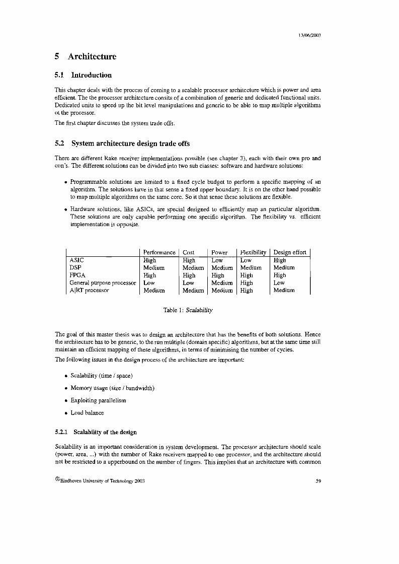
13/0612003
5 Architecture
5.1 Introduction
This chapter deals with the process of coming to a scalable processor architecture which is power and areaefficient. The the processor architecture consits of a combination of generic and dedicated functional units.Dedicated units to speed up the bit level manipulations and generic to be able to map multiple algorithmsot the processor.
The first chapter discusses the system trade offs.
5.2 System architecture design trade ofCs
There are different Rake receiver implementations possible (see chapter 3), each with their own pro andcon's. The different solutions can be divided into two sub classes: software and hardware solutions:
• Programmable solutions are limited to a fixed cycle budget to perform a specific mapping of analgorithm. The solutions have in that sense a fixed upper boundary. It is on the other hand possibleto map multiple algorithms on the same core. So it that sense these solutions are flexible.
• Hardware solutions, like ASICs, are special designed to efficiently map an particular algorithm.These solutions are only capable performing one specific algorithm. The flexibility vs. efficientimplementation is opposite.
Performance Cost Power Flexibility Design effortASIC High High Low Low HighDSP Medium Medium Medium Medium MediumFPGA High High High High HighGeneral purpose processor Low Low Medium High LowAIRT processor Medium Medium Medium High Medium
Table 1: Scalability
The goal of this master thesis was to design an architecture that has the benefits of both solutions. Hencethe architecture has to be generic, to the run multiple (domain specific) algorithms, but at the same time stillmaintain an efficient mapping of these algorithms, in terms of minimising the number of cycles.
The following issues in the design process of the architecture are important:
• Scalability (time / space)
• Memory usage (size / bandwidth)
• Exploiting parallelism
• Load balance
5.2.1 Scalability of the design
Scalability is an important consideration in system development. The processor architecture should scale(power, area, ...) with the number of Rake receivers mapped to one processor, and the architecture shouldnot be restricted to a upperbound on the number of fingers. This implies that an architecture with common
©Eindhoven University of Technology 2003 59

13/06/2003
resources used, is not feasible. A common resource creates a bottleneck. For example a common memoryhas a limited access bandwidth and limits the number of processes that can access the memory in a certainamount of time.
~memory If
•base band processing II, , ,
Figure 65: Common memory resource
A distributed approach can provide better system scalability and exploit better the data parallelism of thealgorithm. The operations in the kernel of the Rake algorithm only use local data, the so-called locality ofreference is preserved.
base bandprocessing
base bandprocessing
c:o base band
processing
Figure 66: Distributed memory resources
To efficiently map the Rake algorithm, the data parallelism has to be exploited.
• The same operations are applied to multiple functional unitsMultiple Rake receivers are mapped onto different functional units (space diversity).
• Conceptually different operations are performed at the same time on different functional units (loadbalance).
60 ©Eindhoven University of Technology 2003

13/0612003
5.2.2 memory usage balance
The concept of Rake receiver is that multi paths belonging to the same transmitter have to combined to onestronger signal (see chapter 2.5). To time align the signals received from different multi paths, the earlyarriving signals have to be delayed until all multi path components have arrived. This delay difference isalso called delayspread. The delayspread is expressed as a multiple of the chip time (Te) or chip period.
The maximum delay spread depends on the mulitpath propagation and soft handover.
It is assumed that:
Maximum delayspread = 256· Te
where Te= chip period
The UMTS chip rate is 3.84 Mchips/sec so:
256chipsMaximum delayspread = = 67 J-L sec
3.84Mchipsj sec
The design of the architecture has to be provided with a memory which is sufficiently large to implementthis delay buffer. The time alignment can be done at chip or symbol level. This choice influences thelocation of the memory:
1. Before despreading
2. After despreading
3. In maximum ratio combiner
When the alignment is done at chip level the memory is placed before correlation. The chips are read frommemory with different offsets for each multipath. The chips alignment is done by reading from memorywith different address offsets.
When the alignment is done at symbol level, the memory is placed after the despreading operation or in theMaximum ratio combiner. Each finger is despreading the incoming chips with a different delay offset, i.e.different start time for correlation and different code offset. The depreaded symbols are stored in memoryfor maximum ratio combining.
The different approaches will be discussed in terms of access bandwidth and memory size.
©Eindhoven University of Technology 2003 61

13/0612003
Memory before despreading The first implementation is placing the alignment memory as a single memory bank before the despreading function, like the FlexRake and DSP solutions.
91ymbob;MRC
LJaddress
Figure 67: Memory alignment before despreading, FJexRake implementation
The key idea of this solution is to first do the time alignment (at chip level) and then process the chipsfurther. The memory bank stores the incoming oversampled chips.
The address of the memory has two fields. The first field specifies the chip location and second field specifiesthe sample to be selected for that chip. These address fields are controlled by the searcher and tracker, i.e.channel estimation! tracking/ synchronization. For each path there is a separate address generated and theselected sample is send to the corresponding finger. By selecting the chips for each multipath from specificlocations in the memory, the time alignment is achieved. The memory serves as a chip selector, by selectinga sample corresponding to a chip, depending upon the information received from the path synchronization.The memory address offset adjustment can also be done by changing the first field of the address for aspecific multi path.
The implications on the hardware requirements will be discussed for this solution. The samples frommemory which are delivered to the Rake receivers, from one base station, are time aligned. The samescrambling code can be used for all Rake receivers. The same holds for fingers receiving the same downlinkchannel, the channelization code generator can be shared.
The total memory size is dependent on the maximum delay spread, expressed in chips, for time alignment.Further it depends on the oversampling rate of the incoming samples, i.e. each (oversampled) sample hasto stored in memory. The memory needs to store a complex sample, I and Q couple, this explains the factorof two.
The memory size can be written as:
Memory size [bits] = 0 •. Dc' chipwidth' 2 (18)
where
0. = oversampling rate
Dc = maximum delay spread
chipwidth = the number of bits to represent one real chip
The memory access bandwidth is dependent on the number of write and read accesses to the single memorybank. Each chip period 0. samples are written to memory and for each finger a chip is read for despreading.For synchronization of each finger an addition 2 chips are used (early-late synchronization).
Bandwidth [Maccessj sec] = Rc . (0. + number of fingers· (1 + 2» (19)
62 ©Eindhoven University of Technology 2003

13/06/2003
Memory after despreading The second implementation is placing the alignment memory in the fingerafter the despreading operation but before the maximum ratio combination. In this way the alignment isdone at symbol level. There are two options that can be chosen with respect to the control of memory.
110 samples
Memory symbolsMRC
Searcher & TracKer
Figure 68: Single memory, alignment after despreading
1. Firstly a single memory bank solution instead of separate distributed delay memories for each Rakereceiver. This implies one common address generator. The memory can split into different parts,each part corresponds to one Rake receiver. The symbols coming from all fingers correspondingto one Rake receiver, are stored in the corresponding part that is reserved. In this way all receivedsymbols corresponding to a transmitted symbol are stored in 4 consecutive memory locations. Witheach completion of the finger that is tracking the longest path, the maximum ratio combination readsthe symbols from four consecutive memory locations and combines them. The memory size forthis solution is reduced by a factor of the spreading factor and oversampling ratio compared to thememory before despreading.But the memory size is also increased because the stored symbols havemore bit precision as stored chips.
Total memory size [bits] =~ . (number of fingers)· symbolwidth ·2 (20)SFmin
where
Dc = chip time
SFmin = minimum spread factor
symbolwidth = number of bits to represent one real symbol
factor of 2 because the symbols are complex (I & Q ).
The memory access bandwidth is linearly dependent on the number of fingers and the spreading factor. AllRake receivers use the same memory, thus the memory access increases.
. Rc (nUmber of fingerS)BandWidth [Maccessj sec] = -- . .' (number of rake receivers) (21)SFmin Rake receiver
where
Rc = chiprate
SFmin = minimum spreading factor
Separate memories for I and Q symbols.
©Eindhoven University of Technology 2003 63

13/0612003
I/Qsamples
symbolsMRC
Searcher & Tracker
Figure 69: Distributed memory, alignment after despreading
2. Another solution is to distribute the memory in separate blocks for each finger. The control of thememory access can then also be distributed, hence reducing the access bandwidth to the memory.
The memory size is the same as the first solution, so:
DTotal memory size [bits] = __c_. (number of fingers)· symbolwidth' 2 (22)
SFmin
where
Dc = chip time
SFmin = minimum spread factor
symbolwidth = number of bits to represent one real symbol
factor of 2 because the symbols are complex (1 & Q ).
The memory access bandwidth is also linearly depended on the number of fingers, but because of thedistributed approach the memory access bandwidth is reduced.
Rc (nUmber of fingerS)Bandwidth [Maccessj sec] =--. .
S Fmin Rake recel ver
where
Rc = chiprate
SFmin = minimum spreading factor
Separate memories for I and Qsymbols.
(23)
64 @Eindhoven University of Technology 2003

13/06/2003
Memory in maximum ratio combiner The last possible implementation of the memory alignment is theplace the memory in the maximum ratio combiner. The maximum ratio combiner combines the symbolsfrom each active finger into a single stronger symbol (see figure 27). Since the fingers may be separatedin time with up to 512Tc=134 /-LS. The memory needs to buffer the partial accumulated symbols until allactive fingers have arrived. The maximum delay between the same symbols from different fingers is 128symbols (SF=4).
The maximum ratio combiner stores the partial accumulated symbols in a circular buffer, which is implemented in a similar way to the stream buffer in the FlexRake solution.
At the moment when the maximum ratio combiner receives a symbol, it first reads the partially accumulated!combined symbol from memory. The received symbol is accumulated with the symbol from memory. Thenewly combined symbol is written to the memory at the same location as the partially combined symbol isread. If the received symbol was from the finger with the largest multipath delay, the accumulated value issent the output port, and the memory location is cleared.
I/Qsamples
MAC
Memory
symbols
address
Figure 70: Memory alignment in Maximum ratio combiner
The memory size will be further reduced because the symbols of the multipath components are partiallyaccumulated, i.e. only one memory location per combined symbol.
DTotal memory size [bits] = __c_ . symbolwidth ·2· (number of rake receivers) (24)
SFmin
where
Dc = maximum delay spread
Tc = chip time
SFmin = minimum spread factor
symbolwidth = the number of bits to represent one real symbol
The memory access bandwidth has the same properties as the memory after despreading solution, so multiple Rake receivers mapped to one physical memory or distributed over multiple memories.
. Rc number of fingersBandwIdth [Maccess / sec] = -- . ( .). (number of rake receivers) (25)
SFmin Rake recel ver
where
Rc = chiprate
©Eindhoven University of Technology 2003 65

13/06/2003
SFmin = minimum spreading factor
The number of Rake receivers is 1 in a fully distributed approach.
66 ©Eindhoven University of Technology 2003

13/0612003
Comparison of different alignment implementations In figure 71 the comparison is presented withrespect to memory size. In figure 72 the comparison is presented with respect to the memory bandwidth.
Os =4
Dc = 512 chips
Rc = 3.84-106 chips/sec
chipwidth = 8 bit
symbolwidth =16 bit
SFworstcase =4
SFbestcase = 256
#fingers/ Rake receiver wors/case = 6
#fingers/ Rake receiver bestcase = 3
Memory size
350000 -,------------------------,!i
300000 +---------------------,--i
250000 +------------------, -----11.. I r --B-e-'o-'e-c-o-rre-la-Iio-n---' I
200000 +---------------".---------1 __ aher correlation [best case]
[
I aher correlation Iworst case]
150000 +-----------,,---,----------i. --+-In MRC Ibesl case]
~ Ii I-+--In MRC (worst case
'~ ~, ; ; ;;: ~ : :::::::o 1 2 3 4 5 6 7 B 9 10 11 12
rake receivers
Figure 71: Memory size vs. rake receivers
@Eindhoven University of Technology 2003 67

13/06/2003
Memory bandwidth
9.E..08
8.E..08
u7.E..08
'"., 6.E..08Vi.,'" 5.E..08uuco
4.E..08~0E 3.E..08'":;;
2.E..08
1.E..08
O.E..OO
0
--.- Before correlation [best case]
1
--.- Before correlation [worst case]
after correlation [best case]
__ after correlation [worst case]
__ In MRC [best case]
__ In MRC [worst case]
2 3 4 5 6 7 8 9 10 11 12
rake receivers
Figure 72: Memory bandwidth vs. rake receivers
In this thesis the assumption was made to have a scalable architecture, this excludes the possiblility ofoption of memory in before correlation. In this solution the memory and code generator is a common unitand gives an upper boundary on the number of fingers that can be mapped. Further the use of common unitsintroduce at layout level more wire length than solutions where the data is kept locally.
From the two resulting scalable I distributed solutions the implementation with the memory in the maximumratio combiner is choosen for implementation, because this solution uses the available memory locationsmore efficiently.
68 ©Eindhoven University of Technology 2003

13/0612003
5.3 Exploiting parallelism
There are two basic techniques that can be used to increase the processor perfonnance:
• Implement the processor in a faster technology.
• Perfonning more operations in parallel.
It has become apparent that more parallelism must be exploited in order to keep up with the increasingsystem perfonnance.
There are a wide variety of architectures known, that attempt to exploit the parallelism available in theapplication programs. For example, pipelined processors and multiple instruction issuing processors, suchas superscalar and VLIW machines, exploit the instruction level parallelism. In contrast, shared memorymultiprocessors typically exploit parallelism by distributing entire loop iterations to different processors.
5.3.1 limitations to parallelism
The parallism available in an application is limited by its dependences. A dependence between two operations is a conflict that prevents the operations from executing concurrently. Dependences can be categorizedinto three types:
I. resource
2. control
3. data
A resource dependence exists between two operations when they both need to use the same physical resource at the same time. These dependencies are a physical limitation of the actual machine on which aprogram is to be run.
A control dependence occurs when an operation should be executed only if a previous operation produces acertain value. For instance, a conditional operation produces a control dependence to a different operationif the second is to be executed only if the condition evaluates to a specified value. In the Rake algorithm theconditional statements are frequently used (see figure 73).
local_ACC_finger1 += despread_chip1 ;if (local_SF_finger1 == 0) {
SymboUinger1 = local_ACC_finger1 ;local_ACC_finger1 = 0;
address =delay_finger1 + counter;mrc_symboUinger1 =MRC[address];MRC[address] =mrc_syrnboUinger1 + SymboUinger1;
I finger symbol dump
I Maximum ratio combining
Figure 73: Ex.ample of conditional code in Rake algorithm
Data dependencies, also known as hazards, are read-write conflicts between two operations in which theyboth access the same storage location, such as a register or location in memory.
©Eindhoven University of Technology 2003 69

13/0612003
In a flow dependence (read-after-write hazard), one operation needs a value generated by a previous operation before the latter operation can begin executing. An output dependence (write-after-write hazard)occurs between two operations when they both write to the same storage location. The correct orderingof these operations is required to ensure that any intervening operations that read this location obtain thecorrect value before it is overwritten by the second operation. An antidependence (write-after-read hazard)exists when a later operation may overwrite a value still waiting to be read by an earlier operation. Bothantidependences and output dependence occur when variable names and registers are reused by the programmer or by the compiler to reduce the number of unique memory locations referenced by a program.They can be eliminated by renaming variables so that a unique value of a variable has a unique name. Thecost of this renaming is a potentially large increase in the memory requirements of the program.
5.3.2 Control dependency: Reduce sequential bottlenecks
From previous chapters can be concluded that:
• There exists parallelism in the baseband Rake processing algorithm.
• A distributed approach has the preference to an architecture with common functional units.
• The available parallelism has to be exploited to speed up the application program.
The consequences of mapping the Rake algorithm on an AIRT processor with a SIMD8 VLIW architecturewill be discussed in terms of dependencies:
• The resource dependence is a physical boundary to the architecture. The size of processor has to beas small as possible.
• The data dependencies are solved by the scheduler of AIRT Designer.
• The control dependence is highly dominant in the Rake algorithm, this causes that the algorithm isexecuted in a sequential manner.
8 Single Instruction Multiple Data9Yery Long Instruction Word
70 ©Eindhoven University of Technology 2003

13/06/2003
Rake algorithm mapped on a VLIW type architecture The AIRT processor template consist of a number of simple heterogeneous processing elements connected to small memories and registerfiles. A singlecontrol unit fetches one (very long) instruction word which is then decoded and broadcast to all functionalunits, and causes a data element to be fetched from register! memory or input port (see chapter AIRT processor template).
Branchcontroller
Figure 74: General VLIW architecture
Each functional unit then executes the instruction on the data it has been given. At the end of the instructionthe the resulting data is written back to register! memory or output port. The processing of these VLIWinstructions is synchronous to the central control unit. Multiple functional units can be initialized in parallel(instruction parallelism) to increase the performance of the processor.
In a single controller architecture the conditional statements are executed in a sequential manner, this sequential behavior forms the bottleneck in exploiting the parallelism in the Rake algorithm .
mrc
finger
rfxt IX+ IX+IXIXIXIXIXIXIL ~I_L-I_"-I_
finger 1 finger 2 finger 3
-1X1-1
X!X: ~
finger N
Figure 75: Serial schedule ofRake algorithm on single thread controller
In a distributed implementation of the Rake algorithm, all rake fingers and maximum ratio combiners can
@Eindhoven University of Technology 2003 71

13/06/2003
be modelled as independent processes. Each process has its own (branch) controller. The processors aremutually connected via a global interconnect (see figure 76).
Figure 76: MIMD VLIW architecture
It can be seen as a pure MIMD (multiple instruction, multiple data) application, in which each Rake fingerperforms a correlation with a completely different code and a different spreading factor.
At the other end the Rake algorithm can be seen as a data-parallel application that can run in a pseudoSIMD mode, with every Rake finger performing the same set of operations on its portion of a distributeddata structure. This is however not directly possible because of the conditional behavior of the Rake fingers,e.g. Conditional dumping of accumulated symbols for each finger. The conditional operations must still beunder local control of each Rake finger.
The resulting processor architecture model is one in which each Rake finger executes the same programinstructions, but has some extended flexibility in local control flow.
72 ©Eindhoven University of Technology 2003

13/0612003
Concept of conditional operations in data path The concept of the conditional accumulation of theRake fingers is shown in figure 77.
Figure 77: Conditional statements in datapath
To map an operation like:
void conditionaltest( const Int< 16> sf, Int< 16> & out) {
#pragma OUT out
Int<16> local...sf=sf;
while(l) {
local...sf -= 1;
if (local...sf == 0) {
local...sf{l] == sf;
out = local...sf;
}//if
}//while
OUTPORTINPORTROMCONTROL
}//conditionaltest
The schedule of the program on a single controller architecture, without placing the control informationlocally in the datapath, is as follows:
The while loop can be seen as a rectangle over the cycles numbers 4 till 10. In the body of the while loopa conditional statement (if statement) is executed in cycles number 9 and 10. The cycles 7 and 8 representthe branch delay.
Cycle ALU2345678910
Sub PassPass
<0>
<1><0>
Read
Write
The condition can be moved from the controller into the datapath, the control information is part of the data
©Eindhoven University of Technology 2003 73

13/06/2003
conditional operations
I
I
I-~
x l ---
I
I XXIXXL..:........: _x
ALU
inport
outport
romcontrol
2 3 4 5 6 7 8 9 10
Figure 78: Conditional schedule
path. The functional unit ALU is extended with an extra data and control input (see figure).
Figure 79: Condition locally in the datapath
This abstract example represents the updating of the spreading factor for each finger. Variable local..sf ismapped to register R31 and variable sf to register R2. In register R4 is constant value 1 is stored.
74 @Eindhoven University of Technology 2003

13/0612003
Conditional Rake finger This example of conditional updating the local spreading factor can be extendedto a complete finger. In figure 80 multiple Rake fingers are time multiplexed on the same ALD.
5 incoming despreaded samples4 accumulated finger value3 subtracted spreading value2 several constants1 control information
3
R3<
R33
R32
5
where:
ALUl
Figure 80: Control data in data path ofALU
ALU2
RlR2R3R4
condition registerspreading factorsubtracted spreading factor values1
condition registeroaccumulated finger valuesincoming despreaded chips
Table 2: ALUregisters usage
The incoming despreaded samples (ALU 2---+R4) are accumulated with the local accumulation value ofeach finger (ALU2---+R31..R34). In ALU 2---+R3l the accumulation value of finger 1 is stored and inALU2---+ R32 the value for finger2 etc.
ALU2---+Rl is a control register that controls the selection of one input of the ALU 2. This register isnormally 1, i.e. the inputs of ALU2 are register R4 and one register of the set R3l ...R34.
ALU 1 controls the updating of the spreading factor for each finger in the Rake receiver, and sets a flagwhen the output of the ALU is zero. ALU 1 subtracts the registers R31 ..R34 with the value 1, each time achip is accumulated in ALU2. When the result of the subtraction is zero, i.e. Rl is zero, the next time notregister R3l ..R34 is selected but R2 (spreading factor of the channel).
Register ALU2---+ R2 (zero) is also selected when register ALU2---+ Rl is zero, this means the local accumulation is dumped to a symbol and the register is resetted to zero.
In next figure a timing diagram is presented of the conditional operations. In the first chip period finger 3completes the accumulation over a spreading factor. The symbol value of finger 3 is send to the maximumratio combiner (not shown in figure). The next chip period the local accumulation register of finger 2 isinitialized to zero. In chip period 2 finger 4 completes the accumulation.
Conditional maximum ratio combining In the single threaded solution the maximum ratio combiningoperation is a conditional operation, executed only at the end of the correlation period. This means that alsothe memory access, for coherent combining, is conditional.
©Eindhoven University of Technology 2003 75

13/0612003
incoming despre.dod samplos :::==X==~:::::;:;==:::;:::::::;:::=ch:::iP:1;:::::::::;==;::;=::::::::;:::::;~X;=:;;::::::::::;=::::;;:=C=hi~P~2=;==:::;:::::;;:=:X~accumulated finger value ~2 -1 -3 -2
subtracted spreading value 2
control information
finger 1 finger 2 finger 3 finger 4 finger 1 finger 2 linger 3 finger 4
Figure 81: Time diagram control flow
When the condition is placed in the data path instead of executed as a conditional branch operation, thememory is access every chip. The behavior of the maximum ratio combining remains the same.
In the next section of pseudo C code the maximum ratio combining operation is presented:
MRC:
if {locaLSF-fingerl ==0) {
address = delay_fingerl+counter;
mrc_symbol = MRC [address];
MRC[address] = mrc_symbol + acc_fingerl;
if {locaLSF_finger2 ==0) {
address = delay_finger2+counter;
mrc_symbol = MRC[address];
MRC[address] = mrc_symbol + acc_finger2;
if {locaLSF-fingerN ==0) {
address = delay_fingerN+counter;
mrc_symbol = MRC[address];
MRC[address] = mrc_symbol + acc_fingerN;
The maximum ratio combining operation is repeated for all fingers (N). The schedule shows a highly serialize operations, multiple Rake receiver have to scheduled sequentially.
A solution to exploit the data parallelism that exist in the algorithm, is'to place the condition (local..5PJingerX== 0 ?) in the data path, the same as in updating the spreading factor. This implies that for every chip a maximum ratio combining operation has to take place, but simplifies the schedule and allows executing multipleRake receivers in parallel. The bandwidth of the memory of one Rake receiver is as a result increased.
The innerloop of the schedule is of length of the maximum number of fingers allocated to one Rake receiver(m). In this approach no communication takes places between the functional units and the controller. Multiple Rake receivers can be placed in parallel, under the control of the same instruction word. The fingersallocated to one Rake receiver are time multiplexed in this schedule, this reduces the area size.
76 @Eindhoven University of Technology 2003

mrc
finger
if {local_SF_finger1 ==0) {address = delay~finger1 +counter;mrc_symbol = MRC[address];MRC[address] = mrc_symbol + acc_finger1;
}
finger 1 'finger 2 finger 3
Figure 82: Serial schedule of MRC operations
IXXXX- --.
mrc 1 XIfinger 1 IX X X X XI
mrc 2 IX XX X XIfinger 2 IX XX X XI
mrc 3 IX XX X XIfinger 4 IX XX X XI
L.- ___
..- C\I C') "d" E.... .... .... ....Q) Q) Q) Q) ....OJ OJ OJ OJ Q)
C C C C OJ;;:: ;;:: ;;:: ;;:: c
;;::
Figure 83: Parallel schedule ofMRC operations
13/0612003
.. ~
finger 1\1
©Eindhoven University of Technology 2003 77

13/0612003
5.3.3 Load balance
It's important that each functional unit is occupied as much as possible. The Rake fingers assigned to oneRake receiver are processed sequentially. The functional units being time multiplexed for performing eachof the operations. This makes sure that each functional unit is efficiently used.
The bottleneck of the Rake algorithm implemented, with the memory alignment in the maximum ratiocombiner, is in the memory access used for the combining. The number of processor cycles is linearlydependent on the number of fingers assigned to one Rake receiver.
On the other hand multiple Rake receivers can operate in parallel, computing in space. The Rake receiversare then assigned to otherfunctional units.
This combination of time multiplexed and space multiplexed operations increases the computational efficiency.
78 ©Eindhoven University of Technology 2003

5.4 processor architecture
!~~::5!IlIl ........ on""'N_C
Figure 84: Rake processor
~
13/0612003
©Eindhoven University of Technology 2003 79

13/0612003
5.5 Benchmark
This chapter presents the final power and area estimations and the operating condition used in the synthesisflow.
5.5.1 Operating conditions
Library: corelib
release v5.0-s005 nov6 2002
PVT Operating conditionmax WCMILtyp WCMILmin WCMIL
5.5.2 Power estimation
process1.501.501.50
temperature125.00125.00125.00
voltage1.101.101.10
OC typebalanced treebalanced treebalanced tree
The power estimation has been done on the veri10g netlist with the functional testbench generated by AIRTdesigner and random input data. The clock rate used in the estimation is 100 MHz.
Diesel version: 2.8Build for: NC-VERILOG v03.30.s003Characterization: CMOS12 core libraryCharacterization: amdc..cmos12Jib/amdc..fdsram.512x32x16ED&T Wiremode1: YESED&T Wire area: 0.000000Wire cap. includes fanin: NODelay back annotation: NO
Process name: CMOS12Char. temperature: 25.00 [Celsius]Char. supply voltage: 1.200 [Volts]Number of library cells: 133Default slope rise: 352.0p [seconds]Default slope fall: 352.Op [seconds]
Evaluation time interval: 0,14.54 ~ seconds
Total initialization energy (Xl as 01 and XO as 10) =Total normal dissipated energy (only 01 and 10) =Total input drive energy (not dissipated in cells) =Total internal energy (only 01 and 10) =
Average normal dissipated power (only 01 and 10) =Average input drive power (not dissipated in cells) =Average internal power (only 01 and 10) =
Total average power (only 01 and 10) =
80
388.18p40.22n56.25n31.33p
2.77m3.87m2.15u
6.64m
[Joule][Joule][Joule][Joule]
[Watt][Watt][Watt]+[Watt]
©Eindhoven University of Technology 2003

13/0612003
5.5.3 Area
I Block report for module 'hiveJake' I Current Module I Cumulative INumber of combinational instances 20 9899Number of noncombinational instances 0 2126Number of hierarchical instances 137 419Number of blackbox instances 0 0Total number of instances 157 12444Area of combinational cells 304.597 126942.399 68%Area of non-combinational cells 0.000 60039.943 +32%Total cell area 304.597 186982.342 100%Number of nets 2319 14567Area of nets 0.000 0.000Total area 304.597 186982.342
• Ar&B 01 CC1mbinnonai cells
• ArBS of non-combinational cBIIs
Figure 85: Pie chart area usage
Normal IC designs have a 80% effective usage of combinational area, due to decoupling capacitance, therefore the estimated area of 0.18 mm2 will after correction ±0.20 mm2.
©Eindhoven University of Technology 2003 81

13/06/2003
5.5.4 Timing report
ReportModuleTimingSlew PropagationOperating ConditionPVTModeTree TypeProcessVoltageTemperaturetime unitcapacitance unitresistance unit
reporUiminghiveJakeEARLY /LATEWORSTWCMILmaxbalanced1.5001.100125.0001.000 ns1.000pF1.000kOhm
EarlyPath 1: MET Hold Check with Pin regin2_COMPARE-1/reg_u_1/queg_1/CP
Endpoint regin2_COMPARE_1/reg_u_1/qrJeg_1/D (v) checked with leading edge of 'elk'
Beginpoint: regin2_COMPARE_1/reg_u_1/queg_lIQ (v) triggered by leading edge of 'elk'
Other End Arrival Time = 0.000Hold = -0.058Phase Shift = + 0.000----...."....,=-Required Time = - 0.058Arrival Time 0.298Slack Time = -----;;0~.3;-;:5~6~
Clock Rise Edge = 0.000-------;~=--Beginpoint Arrival Time = 0.000
LatePath 1: MET Setup Check with Pin u_uromir/queg325/CP
Endpoint: u_uromir/queg325/D (v) checked with leading edge of 'clk'
Beginpoint: rst...a n triggered by leading edge of 'clk'
Other End Arrival Time = 0.000Setup = - 0.103Phase Shift = + 10.000Required Time = 9.897Arrival Time = -8.458Slack Time = ------:-1-:.4-=3""'9-
Clock Rise Edge = 0.000Input Delay = + 1.000Drive Adjustment = + 2.324Beginpoint Arrival Time = 3.324
82 ©Eindhoven University of Technology 2003

13/0612003
5.5.5 Conclusions
In this master thesis an efficient implementation of a scalable WCDMA Rake receiver is presented. By placing the alignment memory in the maximum ratio combiner the architecture becomes scalable and memorybandwidth decreases. The total memory size is linear dependent on the spreading factor and number ofRake receivers.
For low end applications, number of Rake receivers i 8, the total memory size is smaller compared to thememory before correlation.
For basestation applications, number of Rake receivers (, 100, the scalability is important, i.e. the bandwidthto the central memory is not sufficient.
A distributed approach with local memory is in both scenarios a better solution.
The exploiting of the parallelism of the Rake algorithm is in a single threaded solution bounded on theconditional branch instructions. The solution is to place the condition locally in the datapath. This ensuresthat multiple Rake receivers can be scheduled fully parallel (computing in space). The Rake receivers areassigned to other functional units.
To save area size, Rake fingers assigned to one Rake receiver are processed sequentially (space / timeconsideration). The functional units being time multiplexed for performing each of the operations.
This combination of time multiplexed and space multiplexed operations increases the computational efficiency.
The total design consumes
6.6 mW / 0.2 mm2 /100 MHz/ 1.2V = 0.3 mW / mm2/ MHz
@Eindhoven University of Technology 2003 83

13/0612003
References
[1] Nilsson M., Efficient ASIC implementation of a WCDMA Rake receiver, Master thesis, LuleaUniversity of Technology, 2002
[2] Ojanpera T., Prasad R. WCDMA: Towards IP mobility and mobile internet, Univeral Personalcommunications, Artech House Publishers, Gillingham street, London, 2001
[3] Viterbi AJ., CDMA principles of spread spectrum communication, Electrical engineering 1Telecommunications, edition 2, Addison-Wesley, New York, 1995
[4] Turin G.L., Introduction to spread spectrum antimultipath techniques and their application to urban digital radio., In conference proceeding of IEEE volume 68, 1980, pp. 328-353
[5] Tiwari A., Wubben R.H.M., DSP implementation of a Rake receiver, Technical note, Nat.Lab.TN 2000/49, Philips Research Eindhoven, 2000
[6] Texas Instruments, Implementation of a WCDMA Rake receiver on a TMS320C62xx DSP, Application note, SPRA680, 2000
[7] Srnit L.T., Smit GJ.M., Havinga P.J.M., Hurink, J.L., Broersma H., Influences of Rake receiverlTurbo decoder parameters on energy consumption and Quality, In conference proceedingof World Wireless Congress, San Francisco, 2002, pp. 175-181
[8] Singleton c., Tucker c., 3Ghttp://webpages.acs.ttu.edu/vsinglet, 2001
wireless communication systems,
84
[9] Shankiti A., Leeser M., Implementing a RAKE receiver for wireless communications on an FPGAbased computer system, In conference proceedings of FPCI 2000, Monterey 2000, pp.145-151
[10] Rodriguez A., WCDMA FDD simulink models, http://www.mathworks.com.2ooo
[11] Proakis J.G., Digital Communications, Electrical and computer engineering, edition 3, Mc-GrawHill.New York, United States, 1995
[12] Milstein L.B., coherent DS-CDMA performance in Nakagarni multipath-fading, IEEE Transactions on Communications Technology, volume 43, pp. 1134-1143,1995
[13] Meuwissen P., Wubben R.H.M., Vectorization ofthe UMTS-FDD Inner Transceiver: Architecturerequirements for the CVP, Technical note, Nat.Lab. TN 2000/40, Philips Research Eindhoven,2001
[14] Meel J., Spread spectrum(SS): applications, Studiedag Spread spectrum, 1999, Hogeschool voorwetenschap kunst, De Nayer instituut, Leuven, Belgium
[15] Holma H., Toskala A. WCDMA for UMTS: Radio Access for Third Generation Mobile Communication, John Wiley Sons, LTD., Chichester, England, 2000
[16] Harju L., Kuulusa M.,Nurrni 1. A flexible rake receiver architecture for WCDMA mobile terminals, In conference proceedings of Workshop on advances in signal processsing, SPAWC '01,volume 3, IEEE. pp. 9-12, 2001
[17] Couch L. Digital and Analog Communication Systems, edition 6, Prentice Hall, Upper SaddleRiver, New Jersey, 2001
[18] 3rd Generation Partnership Project (3GPP), Services provided by the physical layer (release1999), TS25.302 v3.5.0, Technical Specification Group Access Network (TSGRAN WGl), Technical specification, 2000
©Eindhoven University of Technology 2003

13/0612003
[19] 3rd Generation Partnership Project (3GPP), Physical layer procedures (FDD)(release 1999),TS25.214 V3.3.0, Technical Specification Group Access Network (TSGRAN WGl), Technicalspecification, 2000
[20] 3rd Generation Partnership Project (3GPP), Spreading and modulation (FDD)(release 1999),TS25.213 V3.3.0, Technical Specification Group Access Network (TSGRAN WGl), Technicalspecification, 2000
[21] 3rd Generation Partnership Project (3GPP), Physical channels and mapping of transport channelsonto physical channels (FDD) (release 1999), TS25.211 V3.3.0, Technical Specification GroupAccess Network (TSGRAN WGl), Technical specification, 2000
[22] 3rd Generation Partnership Project (3GPP), VB Radio transmission and reception (FDD) (release 1999), TS25.101 V3.3.0, Technical Specification Group Access Network (TSGRAN WGl),Technical specification. 2000.
©Eindhoven University of Technology 2003 85

Index
Acquisition phaseMatched filter, 24Serial! parallel synchronization, 24Sliding/ active correlator, 24
Antijamming capability, 7
back annotation, 58
CDMA,2Code division multiple access, 2
CDMA2000,2Conventional Rake receiver, 28
Direct sequence, 2, 3Direct sequence spread spectrum, 2DLL, Delay locked loop25DS, Direct sequence 2
FDMA, Frequency division multiple access 7FH, Frequency Hopping 2FIFO, 30FlexRake, 29
Control,31FlexRake receiver, 29
Correlator engine, 30Stream buffer, 30
Frequency Hopping, 2Frequency hopping spread spectrum, 3
HandoverSoft and softer handover, 21
Hybrid modulation, 3
interferencemultiple access interference, 13narrowband interference, 12widebandinterference, 12
Interference rejection, 7IS-95,2
LPI, Low probability of interception7
Maximum Ratio Combiner, 17, 28multi path, 15multiple access, 7Multiple access capability, 6
Near far problem, 13
OVSFOrthogonal variable spreading codes, 9
Post buffer Rake receiver, 32Channel compensator, 37
87
Chip aligner, 32Descrambler, 34Despreader,34MRC,37OVSF generator, 34PN generator, 33Symbol despreader, 36
Post Buffering Rake receiver, 32power control, 14Privacy, 7Processing gain, 2Protection against multipath interference, 6
Rake, 26receiver, 17
Rake receiverConventional, 28FlexRake, 29Post buffering Rake receiver, 32
RF, Radio frequency7
SF, 2SIMD,70Simulink, 42Spreading codes, 9
Channelization code, 11Hadamard-Walsh codes, 11m-sequence, 9Scrambling codes, 10
SynchronizationAcquisition phase, 23Tracking phase, 25
SystemC,47
TDMA, Time division multiple access 7TH, Time Hopping 2Time Hopping, 2Time hopping spread spectrum, 3
UMTS,2
Variable Delay Buffer (VDB), 37VHDL,42VLIW, 42, 47
WCDMA,2Wire load models, 57