from rtl to netlist - budapest university of …gaertner/segedanyagok/veriloglabor/… · web...
TRANSCRIPT

FROM RTL TO SILICON
The Main Steps of Chip Design
Introduction and Primer
Worksheets for students designing VLSI integrated circuits at the VLSI laboratory of the DED (QB310) using the Cadence Design Environment on
PC’s under LINUX Operating System.
dr. Peter Gärtner
The 15th April 2014
15.04.2014. PG. 1

CONTENTS
Introduction 3
Itinerary Through the Design 4
Part One: From RTL to Netlist 5
1.1. Prepare for working with the tools 51.2 Check the verification of the Verilog description 61.3. Check the sinthesizability of the Verilog description 101.4. Preliminary synthesis without I/O pads 111.5. Pre-layout simulation with Questa 121.6. Add pads to the design 121.7. Final synthesis 141.8. Add power pads to the top-level Verilog netlist 15
Part Two: Building the Chip 16
2.1. Preparations 162.2. Load the project into EDI91 162.3. Make I/O-Assignments 182.4. Set up the floorplan 182.5. Prepare the power network 192.6. Do placement 222.7. Check the layout without clock-tree 222.8. Synthesize the clock tree 232.9. Finish the placement 252.10. Routing 262.11. Verification 272.12. Extract the new netlist 282.13. Extract timing information for post-layout simulation 282.14. Post-layout Simulation 28
15.04.2014. PG. 2

Introduction
It is true that the functionality of a chip is created in the logic design phase but the Verilog description is only software. Further steps are directed towards giving it an optimal physical form while maintaining the functions. The majority of the activities are tiresome routine jobs, many of the steps can be done automatically. Yet they are important because without them the chip could not be manufactured. During the semester you have to design an ASIC chip for a given specification. First you have to complete the exciting and interesting logic design which results in a verified RTL level Verilog description. The brochure Verilog for Synthesis describes the way how to arrive at that objective. However, the simulator Questasim will be needed after synthesis, therefore, a short overview is given here about it for those who did the Verilog part by means of another simulator. Then the first part of this brochure will take you through the synthesis part of the design work. The second part describes the building of the chip layout: floorplanning, placement and routing. Even if the design work mainly consists of routine activities, the synthesis as well as the placement and routing are also exciting and interesting, and they can get the designer sweating. Anyhow, they are also part of the tasks of the ASIC designer and, therefore, you have to learn and exercise it.Nowadays chip design can be subdivided into three main phases, each of which is closely connected to a design tool:1. The Verilog phase. (Logic design) The idea and/or necessity gives rise to a specification
which is then coded in a hardware description language (HDL), in our case Verilog, but it might also be VHDL, and is verified by simulation. The coding usually starts on a behavioural level and is partitioned and refined until arriving at the RTL (register transfer) level. These activities can be done with any Verilog simulator if you observe the syntax of the standard Verilog language. They are covered in the brochure “Verilog for Synthesis”.
2. The synthesis phase. It consists of two not sharply separated steps: a) conversion into a technology-independent generic gate-level netlist (“elaboration”) and b) its mapping into the elements of a cell library of a given technology which is intended for the realization of the chip. Both steps are performed under optimization constraints aiming at silicon area and/or time (propagation delay). The result is a netlist containing the cells of the target technology. Our synthesis tool is Cadence RTL Compiler, shortly RC, which delivers a gate-level netlist. The netlist can (and has to) be verified by the Verilog simulator Questa of Mentor Graphics (pre-layout simulation) before starting the last phase, the physical (layout) design, by placement and routing. The target technology is AMS 0,35µm, 3 metal layers. This is the topic of the first part of this brochure.
3. The layout phase. The cells of the target technology are described with different views. The synthesis has used the view containing the logic model and timing of the cells. Now it comes to the layout view or its simplified version, the graphic phantom. The graphic phantom describes only those parts of the layout which are relevant for the placement and routing, mainly the metalization. The netlist contains the component cells of the chip and their connections. Based upon this information:
a floorplan has to be estimated, the cells have to be placed, the clock tree has to be synthesized, the connections have to be implemented (routing).
Roughly speaking the layout design consists of these steps, which can be performed using the tool Cadence EDI11 (Velocity). Eventually the post-layout simulation verifies and completes the design work. These activities are covered in the second part of this brochure.
15.04.2014. PG. 3

Itinerary Through the DesignThe steps described in the 2nd and 3rd phases really cover the essential tasks of the design from RTL to the layout. However, the description is very much simplified. In order to give a good overview, a lot of “small chores” have not been mentioned at all. They belong to two main groups: creating auxiliary parts on the chip, mainly the power supply, without which the chip could not work, and preparing and establishing the background for the tools, without which they could not work. Next a detailed list of these small chores is given, together with the “great steps”, possibly in the order of their execution.Part One: From RTL to Netlist
1.1. Prepare for working with the tools: Questa, RC and Velocity.1.2. Check the verification of the Verilog description if it was made somewhere else.1.3. Check the sinthesizability of the Verilog description. (Make a generic netlist.)1.4. Preliminary synthesis without I/O pads.1.5. Pre-layout simulation with Questa (functionality check of the synthesis).1.6. Add pads to the design. (Construct a top-level Verilog description
with pads around the core.)1.7. Final synthesis with pad-cells.1.8. Add power pads to the top-level Verilog netlist.
Part Two: Building the Chip2.1. Preparations2.2. Load the project into EDI912.3. Make I/O-Assignments2.4. Set up the floorplan2.5. Prepare the power network2.6. Do placement2.7. Check the layout without clock-tree2.8. Synthesize the clock tree2.9. Finish the placement2.10. Routing2.11. Verification of geometry and connectivity2.12. Extract the new netlist2.13. Extract timing information for post-layout simulation2.14. Post-layout Simulation
15.04.2014. PG. 4

PART ONE: FROM RTL TO NETLIST
In the followings a detailed description of the design-steps 1.1. to 1.8., listed in the itinerary, will be given. Starting from RTL-Verilog they bring the design to a flat netlist. However, we will give a short overview of the simulator Questa, too.You have to get a good overview of the Verilog files and modules which you will encounter during the design activities. You can do it by having a good directory structure and carefully selected file and module names. As you go on with your design, you will have files of similar structure and slightly different modules. In order to keep clearness in your design environment you must not have two files with identical names as well as two modules with the same name. Everything must be simulated using the same stimuli. For this purpose you have one testbench and you will only modify the name of the module to be tested. So far you have a top RTL module. Give it the name projectname_rtl and place it into a file projectname_rtl.v. The test-bench should be called tb_projectname and be placed into a separate file tb_projectname.v. The top module may invoke instances of different sub-modules but their names will not play any critical role. 1.1. Prepare for working with the tools: Questa, RTL Compiler and Velocity. Later on you may work with the GUI of Linux but these first steps have to be done in a terminal shell. In order to maintain clear overview a dedicated data structure has to be set up. Open a terminal shell. Type source /home/eet/tutors/gaertner/cadence6/inifiles/initproject <ENTER>
The script first requests you to input (type) the name of your project (one single word).Thenn this script performs the following tasks:
creates a subdirectory (folder) with the given name <projectname> creates in projectname several new subdirectories:
RTL for the Verilog description with two subdirectories:o Developing for working on the project ando Verified for the final HDL (Verilog) version
Synth for RTL Compiler with two subdirectories o VeriAddPad for adding pad-cells to the core-design ando VeriBackAnnot for doing the back-annotated simulation
PlaceRoute for Velocity. copies the setup file of Linux .bashrc to your home directory. This script is always
executed when you log in to the system and defines several aliases for the session. copies the setup file of Questa modelsim.ini to your home directory copies the setup file of RTL Compiler rcintro.cmd to Synth copies 11 files to PlaceRoute: the clock tree specification file chip.ctstch,
init.globals, corners.io, ASIClab.view, ASIClab.sdc for initialization as well as 6 command-script files.
At this point make a logout and log in again. This will activate the newly acquired .bashrc setup file. Then check it by typing "lth<ENTER>". The list of the recently generated/modified files should appear. Next type “eb<ENTER>”. The text-editor opens with .bashrc. Look at the alias-definitions. You will find cdrc addressing your new subdirectory for synthesis and cdsoc addressing PlaceRoute.
While developing your project you may have created many different files. Wether you did it somewhere else, or in the subdirectory RTL/Developing, now copy the final version to RTL/Verified.
15.04.2014. PG. 5

1.2. Check the verification of the Verilog description. Questa is our golden simulator. Even if you verified your design somewhere else, in our system it has to be checked with Questa.Start Questa by double click at its icon on the desktop. The main window of Questa opens together with the Jumpstart window. Close the Jumpstart window because in this session it is not needed. Questa comes up with the Library pane showing the available libraries. (Fig. 1-1.) Check if among others amscells is also displayed. Click at the “+” sign left to the name. A long list of elementary cells should be displayed.
Fig. 1-1. Starting QuestaComing up from the desktop Questa does not know, where to work. You have to tell it by a left click to
FileChange Directory then the window Choose folder opens (Fig. 1-2.).
Fig. 1-2. Choose folder window
15.04.2014. PG. 6

Here the subdirectory RTL/Verified has to be selected where you placed the final (?) version of your design. Now you start a new project by a left click to
FileNewProject then the window Create Project opens (Fig. 1-3.).
Here you have to give the project a name, define it as <myprojectname>_rtl – because you are going to simulate the RTL description. Let the working (sub)directory remain the default work. (It takes a couple of seconds till Questa generates work and is ready to go on.) After clicking at OK the Add items to the project window opens (Fig. 1-4.). Here you have to specify your Verilog files.
Fig. 1-3. Create Project window
Click at the icon Add Existing File and select in the browser <myprojectname>_rtl.v. You have to repeat this action until you have entered all the files into the project which belong to it. Then close the window. If you select the tab Project pane at the lower part of the main window then you can see all your specified files listed there with a question-mark right of them (Fig. 1-5.).
Fig. 1-4. Add items to the Project window
Fig. 1-5. Specifying the projectNow the simulation project has been specified, so it has to be compiled. Left click at
CompileCompile All
15.04.2014. PG. 7

It takes a couple of seconds and then the successful compilation should be reported in the Transcript pane at the lowest part of the main window. At the same time the question-mark is replaced by a green check-mark for each successfully compiled file (Fig. 1-6.). If you change back to the Library pane now then you will see a "+"sign left to the working directory work. Clicking at it the hierarchy of your modules will be displayed.
Fig. 1-6. After compilationNow Questa is ready to run the simulation. Left click at
SimulateStart SimulationThe Start Simulation window opens (Fig. 1-7.). Here click at the tab Design and select
work tb_projectname
Fig. 1-7. Start Simulation windowIf you simulate on RTL level then you have to skip the next step and start the run. If you happen to simulate already the synthesized cell-level netlist consisting of the logic cells then you have to add the cell-library, too:
Click at the tab LibrariesAdd The Select Library window opens (Fig. 1-8).You can activate the roll-down list by clicking at the black triangle at Browse. Here you have to select amscells. If the switch OK remains grayed then something is missing, you have to check for it (Fig. 1-9.).In addition, if you do postlayout simulation then you have to switch to the tab SDF and there select and add the extracted capacitances
which are contained in the .sdf file.
Fig. 1-8. Specifying the cell-library amscells
15.04.2014. PG. 8

Fig. 1-9. Questa is ready to simulateClicking at OK the simulator prepares for the run. The Waveform pane opens and in the blue Ojects field the names of the pins will be displayed. Should they not appear, then you can clkck at ViewWave and ViewObjects. In the main window the Sim tab has to be activated. The Objects pane contains the node names of the block, selected in the Instance pane on the left of the main window.Select the names of the pins of the main module and then right click at
AddTo WaveSelected SignalsThe selected names appear at the left part of the waveform pane (Fig. 1-10.).
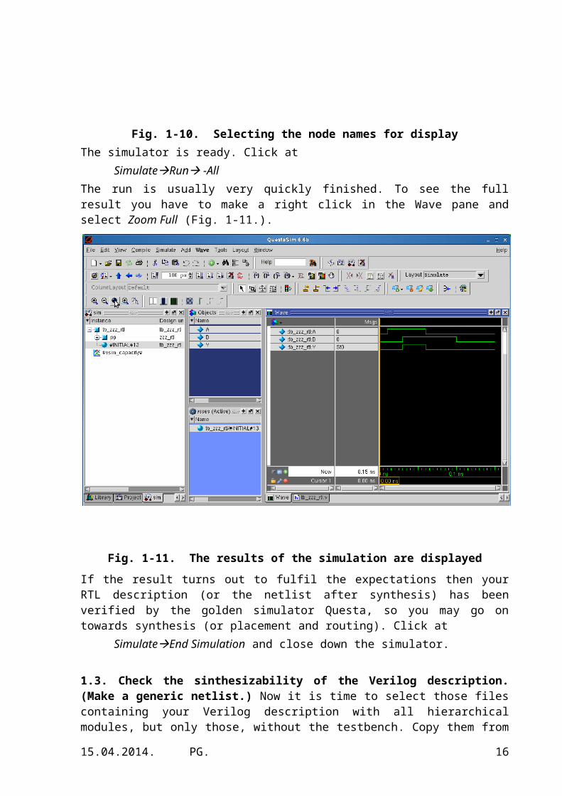
Fig. 1-10. Selecting the node names for display15.04.2014. PG. 9

The simulator is ready. Click atSimulateRun -All
The run is usually very quickly finished. To see the full result you have to make a right click in the Wave pane and select Zoom Full (Fig. 1-11.).
Fig. 1-11. The results of the simulation are displayed
If the result turns out to fulfil the expectations then your RTL description (or the netlist after synthesis) has been verified by the golden simulator Questa, so you may go on towards synthesis (or placement and routing). Click at
SimulateEnd Simulation and close down the simulator.
1.3. Check the sinthesizability of the Verilog description. (Make a generic netlist.) Now it is time to select those files containing your Verilog description with all hierarchical modules, but only those, without the testbench. Copy them from Verified to the subdirectory Synth for the synthesis.Start RC in a terminal shell. Open a terminal shell. Type "cdrc<ENTER>". This alias brings you to the subdirectory Synth. Here you can start RC by typing "rc<ENTER>". RC is controlled from the command line. First a setup script has to be read in. Type
“include rcintro.cmd<ENTER>”. Now RC is prepared and can read in your project. Type
“read_hdl projectname_rtl.v”.RC sends a lot of info messages, but be careful if there are warnings, they have to be checked.If your design is divided into several files, then the read_hdl command is slightly different:
“read_hdl -top <topmodulname> file1.v file2.v … “And here you arrive at the most important step, converting the functional (RTL) description into structure. Type
“elaborate<ENTER>”Now RTL Compiler generates a generic netlist, containing generic logic cells, connected
15.04.2014. PG. 10

together to implement the expected function. If you do not get error messages here, then your functional RTL description is synthesized into a logic cell structure.
Type “gui_show<ENTER>”.
The GUI (graphic user interface) window opens and you can inspect the generated schematic (Fig. 1-12.). If your Verilog description contains hierarchical blocks, you should be able to recognize them in the schematic. The GUI has hardly any functions except for inspection, so you may close it typing “gui_hide<ENTER>” and go on with the sinthesis, without closing down RTL Compiler itself.
Fig. 1-12. Inspecting the generic schematic
1.4. Preliminary synthesis without I/O pads. After the generic synthesis succeeded without errors you can just continue with mapping. Type
"synthesize –to_mapped<ENTER>”.
RC will replace the generic cells of your design by members of the AMS 0.35µm cell library. At this point you may switch on the GUI again and inspect the schematic of the final version of your design (Fig. 1-13.).
Fig 1-13. Inspecting the final netlist (without pads)
15.04.2014. PG. 11

Now it is time to check if the synthesized netlist works. It will be done using the simulator Questa. Therefore type
"write_hdl –mapped projectname > projectname_synth.v".RC writes out the netlist in Verilog format in the file projectname_synth.v. At this point RC may be closed down by typing "exit<ENTER>” because it won't be needed for a while.The top module will still have the name projectname_rtl, as it was in the functional description. In order to avoid identical modul names, it has to be changed to projectname_core by a text-editor. Type
"ed projectname_synth.v<ENTER>”. The editor gedit opens and you can do the change. But there is just one more task to do. Insert the next line into the Verilog file:
`timescale 1ns/1psThis line must be the very first line in the file. Be careful with the "tick" character >>`<< and don’t put a semicolon at the end of the line because it ends in error message. Save and close the editor and move the file to the subdirectory VeriAddPad:
"mv projectname_synth.v VeriAddPad<ENTER>” (See cut-and-paste in Windows.)
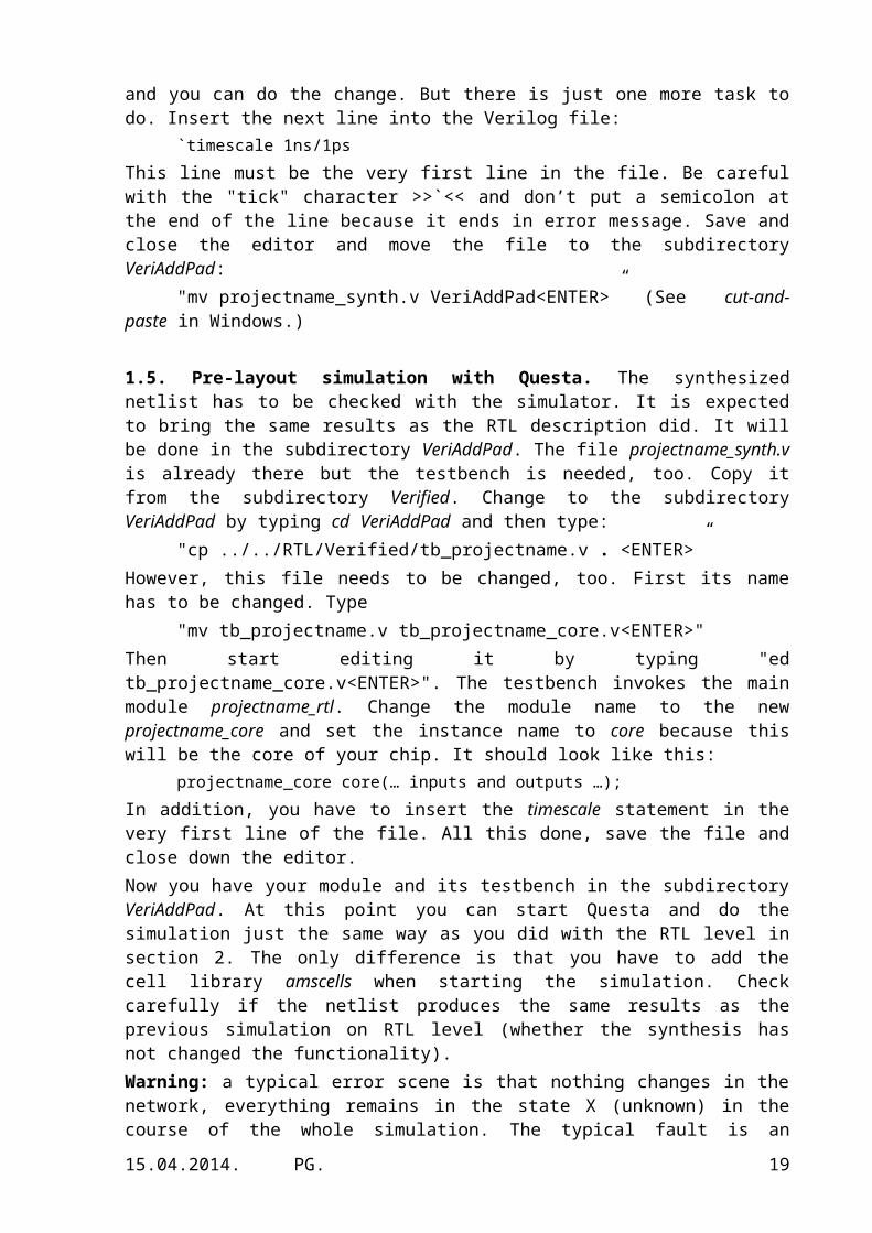
1.5. Pre-layout simulation with Questa. The synthesized netlist has to be checked with the simulator. It is expected to bring the same results as the RTL description did. It will be done in the subdirectory VeriAddPad. The file projectname_synth.v is already there but the testbench is needed, too. Copy it from the subdirectory Verified. Change to the subdirectory VeriAddPad by typing cd VeriAddPad and then type:
"cp ../../RTL/Verified/tb_projectname.v . <ENTER>”However, this file needs to be changed, too. First its name has to be changed. Type
"mv tb_projectname.v tb_projectname_core.v<ENTER>"Then start editing it by typing "ed tb_projectname_core.v<ENTER>". The testbench invokes the main module projectname_rtl. Change the module name to the new projectname_core and set the instance name to core because this will be the core of your chip. It should look like this:
projectname_core core(… inputs and outputs …);In addition, you have to insert the timescale statement in the very first line of the file. All this done, save the file and close down the editor.Now you have your module and its testbench in the subdirectory VeriAddPad. At this point you can start Questa and do the simulation just the same way as you did with the RTL level in section 2. The only difference is that you have to add the cell library amscells when starting the simulation. Check carefully if the netlist produces the same results as the previous simulation on RTL level (whether the synthesis has not changed the functionality).Warning: a typical error scene is that nothing changes in the network, everything remains in the state X (unknown) in the course of the whole simulation. The typical fault is an oversized clock frequency generated by the statement
always #1 CLK = !CLK;This means 500MHz (1+1nsec) which is too high for the cell library. Add one or two zeros after "#1" and reorganize the complete testbench accordingly. Now the network will work.
1.6. Add pads to the design. The core of the would-be chip is ready, its synthesizability has been checked. This module will form the main part of the highest-level module describing the whole chip. Now a top level module has to be created, possibly in a separate file, which should have the name projectname_top.v. The core remains in the file projectname_synth.v. The file projectname_top.v contains only the top-level module which should be called
15.04.2014. PG. 12

projectname_top. It will invoke the core and contain the I/O-pads. In order to use the same test-bench, the top-level module shall have I/O pins with the same name as the core module does. Therefore, the core module has to be instantiated in the top-level module with slightly different pin-names, e.g. with a postfix _c added. This will indicate that they are the same signals, but inside the padring, in the core. The pads, establishing the connection between the outside world (package) and the core, each one will have an input and an output pin with the same name, however, one of them will be distinguished by the postfix _c at the core-side. There are no generic pad-modules in Verilog. The pad-cells of the chosen technology (AMS 0.35µm) have to be added. They are ICP for the inputs and BU1P for the outputs. The instance name of the pads should refer to their signal but they must not be identical. The simplest way to create meaningful pad-names is to add p to the signal name for single variables and p0, p1, p2, etc. for buses. A simple example is for the top module projectname_top(clk, aa, bb, cc, jj, kk, ll).. (Pads for the power supply will be built in only after synthesis.) The main clock input should have the name clk. The file begins with the timescale statement:
`timescale 1ns/1ps
module projectname_top(clk, aa, bb, cc, jj, kk, ll);input clk, aa, bb;input [1:0] cc;output jj, kk;output [1:0] ll;// wires from the package to the pins of the padswire clk, aa, bb;wire [1:0] cc;wire jj, kk;wire [1:0] ll;// wires from the core to the pads:wire clk_c, aa_c, bb_c;wire [1:0] cc_c;wire jj_c, kk_c;wire [1:0] ll_c;
// the core is instantiated with the name “core”:
projectname_core core(clk_c, aa_c, bb_c, cc_c, jj_c, kk_c, ll_c);
// input pads, based upon the module ICP(PAD, core)
ICP clkp(clk, clk_c);ICP aap(aa, aa_c);ICP bbp(bb, bb_c);ICP ccp0(cc[0], cc_c[0]);ICP ccp1(cc[1], cc_c[1]);
// output pads, based upon the module BU1P(core, PAD)
BU1P jjp(jj_c, jj);BU1P kkp(kk_c, kk);BU1P llp0(ll_c[0], ll[0]);BU1P llp1(ll_c[1], ll[1]);
endmodule
When constructing the description by means of a text editor be careful about what to add and where, and check it afterwards! The best check is to simulate it once again. Change the invoked projectname_core module to projectname_top in the testbench by the text editor. Now run the simulator with these 3 files and correct the top module if necessary. Then copy your files back to Synth.
15.04.2014. PG. 13

1.7. Final synthesis with pad-cells. These steps are identical with those for the core, described in sections 3. and 4, applied for the top-level module. However, with the exception of very low clock frequencies (a couple of MHz or lower), the timing behaviour, too, has to be verified. For this purpose the mapping and optimization (see section 3.) has to be extended to timing as well.Therefore define a clock after elaboration, period is given in picoseconds:
“define_clock –name clk –period 100000” (100ns 10MHz)Now you can do mapping (synthesize –to_mapped) and have RC write out a cell-level netlist:
“write_hdl > projectname_pad.v” and then close down RC.
Fig. 1-14. Synthesized core and pads
The new Verilog file projectname_pad.v already contains the signal-pads together with the core, but it still has the hierarchic module structure (Fig. 1-14.). However, for the physical (layout) design a flat netlist is needed. For flattening the design you have to start RC again, include the introductory file and then read the netlist:
“read_netlist projectname_pad.v”The next command does the flattening of the core, the pads are built-in flat:
“ungroup –flatten core”Then the flat netlist is generated:
“write_hdl > projectname_flat.v”Now the netlist is nearly ready, you can use “gui_show” and inspect it (Fig. 1-15, next page). The only missing items are the power-pads. They will be added in the next section.
Fig. 1-15. The flat netlist
15.04.2014. PG. 14

1.8. Add power pads to the top-level Verilog netlist. Having no logic function, RTL Compiler, while optimizing, would delete the power pads. Therefore, they can be added only now, after the synthesis. Copy your top-level file projectname_flat.v from synth to PlaceRoute and open it with the text editor. Depending upon how many power pads are needed (2x2 as a minimum), the following statements have to be inserted into the Verilog netlist, possibly at the end:
GND3ALLP gnd1();GND3ALLP gnd2(); ...VDD3ALLP vdd1();VDD3ALLP vdd2(); ...
So your chip will have two pins for each power connection. Rename the new file projectname_chip.v. This will be the starting point for designing the physical layout.
15.04.2014. PG. 15
PART TWO: BUILDING THE CHIP
This job will be done using the CAD tool Velocity (or EDI11 Encounter Digital Implementation 10.11.) executing the steps 2.1. to 2.13. as listed in the Itinerary (page 4). The following pages provide detailed instructions for these activities.2.1. Preparations. Start a terminal window. Change the directory to PlaceRoute by typing cdsoc. Type ll and check if all necessary files are copied here:
chip.ctstch (clock tree specification file)init.global (configuration file for EDI11) ASIClab.view, SDC/ASIClab.sdc (timing data for EDI11)corners.io (completes the padring by adding corner-pads)fillperi.cmd (fills up empty places in the padring)AddCorePowerRing.cmd (generates the power-ring for the core)addcap.cmd (closes down the edges of the cell rows)fillcore.cmd (fills up empty places in the cell rows)SRpower.cmd (connects the core power ring to the core and to the power pads)
These files contain instructions for EDI11 which are not project-specific. The command scrips will be entered to EDI11 at the terminal prompt preceeded by the keyword source.Now copy to this directory your synthesized flat Verilog netlist (projectname_chip.v), containig already the power-pads, too.
2.2. Load the project into EDI11. Change to the subdirectory PlaceRoute by typing cdsoc and start EDI11 by typing velo. EDI11 comes up with its main working window and, by the same time, converts the terminal to its logging and command window. The prompt is changed to velocity n>. Here you will receive messages about the activities of EDI11, and, also here, you can enter command scripts, typing source xxxx.cmd. The main window is shown in Fig. 2-1. on the next page, combined with the Design Import window.Click FileImport Design – the empty Design Import window opens (Fig. 2-1.). Click at Load down in the middle. The Load Import Configuration window opens. Go down to PlaceRoute. Select here init.global and click Open. Several data appear in the Design Import window. In the Netlist field correct the Files box to the name(s) of your netlist file(s) and enter the top cell name. Check if there are entries in the box LEF Files. At the Power field Check the Power Net entries: vdd! vdd3o! vdd3r1! and vdd3r2. Check also the Ground Net entries: gnd! gnd3o! and gnd3r. (vdd! and gnd! form the power supply for the core, the others are there for the pads.) Click at Save. The Save Input Configuration window opens. Select the PlaceRoute folder. Enter the filename <projectname>.global and click Save. Click at OK and then type f (for Fit). The first version of the floorplan appears with the pads in a random order (just as they were found in the netlist). Now you can have IDE11 write out a padpreplacement file which you can reorder by means of a text editor.Click at FileSaveI/O File. The Save IO File window pops up. In the browser of this window go down to PlaceRoute. Enter the file name PadPreplacement.io. (Fig. 2-2.). Accept it with OK. Then exit Encouter: FileExit.
Fig. 2-2. The Save IO File window
15.04.2014. PG. 16

Fig. 2-1. Combined windows: the main window and the Design Import window (File Import Design)
2.3. Make I/O-Assignment. As you left Encounter, type in the terminal ed PadPreplacement.io. The editor gedit starts with the io-file. It contains a list of the pads in the order as they were placed in the first version of the floorplan. First of all save a backup for the file, e.g. PadPreplacement.bak. Now you can rearrange the pads arbitrarily, according to your plans/specifications by exchanging the names of the pads – but do not change anything else. The positions remain as they are. In order to avoid certain complications follow the next rule. The power pads (2x2) should be placed in the horizontal rows: vdd1 and gnd1 at the top, as the second and third from right. Vdd2 and gnd2 should be placed at the bottom, as the second and third from left. The signal pads may be arranged freely, possibly forming logical groups according to their function. Save the corrected PadPreplacement.io and exit the editor.
2.4. Set up the floorplan. Start Encouter again typing velo. Click FileImport Design – the empty Design Import window opens. Click at Load. The Load Import Configuration window opens. Now load the new configuration file <projectname>.global. The Netlist, Technology and Power boxes should stay unchanged. In the Floorplan box start the browser on the right side of the entry field for the IO Assignment File and open the newly edited PadPreplacement.io. Similarly, in the Analysis Configuration box search for and open the file
15.04.2014. PG. 17

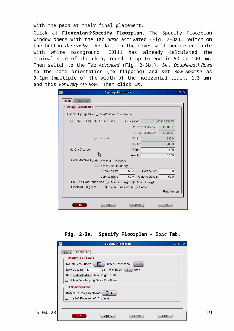
ASIClab.view. Thereafter the completed configuration has to be saved again in <projectname>.global (click Save …). The import of the design is finished. Click OK, the Design Import window closes. The second version of the floorplan appears in the main window with the pads at their final placement.Click at FloorplanSpecify Floorplan. The Specify Floorplan window opens with the Tab Basic activated (Fig. 2-3a). Switch on the button Die Size by. The data in the boxes will become editable with white background. EDI11 has already calculated the minimal size of the chip, round it up to end in 50 or 100 μm. Then switch to the Tab Advanced (Fig. 2-3b.). Set Double-back Rows to the same orientation (no flipping) and set Row Spacing as 9.1µm (multiple of the width of the horizontal track, 1.3 μm) and this For Every <1> Row. Then click OK.
Fig. 2-3a. Specify Floorplan – Basic Tab.
Fig. 2-3b. Specify Floorplan – Advanced Tab.
15.04.2014. PG. 18
The next step is to complete the padring. Click FileLoadI/O File (Fig. 2-4.). Select corners.io, then click <Open> and then ViewRedraw. Now the corner cells are at their place.
Fig. 2-4. The Load IO File window.
At the Terminal Prompt type source DefGlobNet.cmd and then source fillperi.cmd. The first script specifies the global power nets, the second one fills up the gaps in the padring. Inspect the complete padring after Redraw.In the second icon row click at the rightmost icon “Physical view” (Fig. 2-5). In the list of the displayed objects activate the display of the CellInstance Pin by checking the box in the line. Now it is time to save the functionable floorplan which you can return to if something goes wrong (Fig. 2-7., next page). Click FileSave Design. The Save Design window pops up (Fig. 2-6), with the name <projectname_top>.enc. Change top to FP for floorplan so it can be easily distinguished from other saved data, and click OK.
Fig. 2-5. Changing the view
Fig. 2-6. The Save Design window
2.5. Prepare the power network. Type source AddCorePowerRing.cmd. A double ring appears between the core and the pads, for the special global nets vdd! And gnd! In order to reduce the impedance of the power supply of the cells broad vertical metal stripes (M2) are placed in the core, usually 1, 2 or 3 as needed. Click at PowerPower PlanningAdd Stripe. The Add Stripes window opens (Fig. 2-8. page 21). In the Nets field only gnd! and vdd! Are necessary, delete the others. Set Width=14 μm and Spacing=1.4 μm. Switch on and specify the number of sets as 1. In the lowest field specify the horizontal coordinate. Check the button Relative from core Set X from left: ca. half core. It can easily be measured using the Ruler (it is activated by typing <k> and it can be switched off by typing <K>) and after entering it click OK. The next preparatory step is closing down the rows by cap-cells. It is done by the script addcap.cmd (source …).The last step in power planning is that the power leads of the rows have to be connected to the ring and the stripes as well as the ring has to be connected to the power pads. This is done by the script SRpower.cmd (source…).
15.04.2014. PG. 19

Fig. 2-7. The complete floorplan
If all this is correctly done then we save the state adding PW to the name. projectname (DesignSave Design). Fig. 2-9. shows part of the power network.
Fig. 2-9. Power ring connected to the power pads, stripes and to the cell-rows.
15.04.2014. PG. 20

Fig. 2-8. The Add Stripes window
2.6. Do placement. Here it comes to the placement of the core cells. Click at PlacePlace Standard Cell. The Place window opens. You can leave the default Run Full Placement and click at Mode. The Mode Setup window opens. Select from the List of Modes the item Placement. Set Congestion Effort to Medium and give OK, and then in the Place window once more OK. (See the relevant pictures on Figs. 2-10/a/b/c.). At this point you have to save your project adding _PL0 to the name.
Fig. 2-10/a. The Placement window
15.04.2014. PG. 21

Fig. 2-10/b. The Mode Setup window
Fig. 2-10/c. Placement of the standard cells
2.7. Check the layout without clock-tree. The synthesizer program does not build a clock-tree, the clock inputs of all flipflops are connected to the output of the clock pad. They all form a large net, clk_c. The clock tree is synthesized by IDE11 but before doing that step you have to see, what it looks like without the clock tree. For this purpose you have to make a routing. Left click RouteNanoRouteRoute. The NanoRoute window opens (Fig. 2-11/a).
Fig. 2-11/a. The NanoRoute window
15.04.2014. PG. 22

Check if in the block Routing Phase the items Global Route and Detail Route are switched on. Check both boxes for Post Route Optimization: Optimize Via and Optimize Wire and then give OK. When routing is done save the design adding _RT0 to the name. Then zoom to the output region of the clock pad (select the area with a right drag). Then left click on the output line. Check undernieth the graphic window if the net is really clk_c. If it is so then make a full zoom by typing F. The complete net clk_c is now highlighted, quite a wild mesh of white lines. If you switch off the display of the layers on the right pane then it is easier to inspect (Fig. 2-11/b). This kind of clock supply is not recommended, because of the high load on the output of the clock pad. Instead, a clock tree has to be synthesized, see next step.
Fig. 2-11. Simple clock net without tree.2.8. Synthesize the clock tree. First you have to go back to the previous phase PL0. Left click FileRestore Design. Select projectname_PL0.enc and OK. The result of cell placement is displayed again. Left click ClockSynthesize Clock Tree. The Synthesize Clock Tree window opens (Fig. 2-12).
Fig. 2-12/a. The Synthesize Clock Tree window
Click at the browser symbol (…), so the Clock Specification Files window opens (Fig. 2-13).
Fig. 2-13. The Clock Specification Files window
15.04.2014. PG. 23

Click at the arrows (<<). The window changes to a browser. (Fig. 2-14.) Here go to the directory PlaceRoute, select the file chip.ctstch. Now you click at the button Add, and then Close. In the Clock Synthesis Window the name of the selected specification file appears. Click OK and after a short while the synthesized clock tree will be displayed in the main pane together with a preliminary routing.
Fig. 2-14. Select and add chip.ctstch from PlaceRoute
Now you can inspect it by clicking ClockDisplayDisplay Clock Tree. The Display Clock Tree window (Fig. 2-15) opens. Set All Clocks (Clock Selection), Clock Route Only (Route Selection) and Display Clock TreeSelected Level. Select a level and click OK. The routing of the selected level will be highlighted in the main layout pane (Fig. 2-16). You can switch it off by a left click in the pane and start the procedure for the display of another level.
Fig. 15. The Display Clock Tree window
15.04.2014. PG. 24

Fig. 16. Clock tree: the lowest level (No. 3) of the tree.
Inspect all the levels. Notice that the first level brings the clock signal to the middle of the chip, the first distribution takes place there. The lowest level, here No. 3, forms small groups of flipflops placed near to each other.2.9. Finish the placement. The rows have to be filled up, this happens by typing source fillcore.cmd If this is correctly done then we save the state adding _PL to the name. Part of the chip is shown in Fig. 2-17.
Fig. 2-17. Prepared for routing. Notice the filling cells and the power connections.
15.04.2014. PG. 25

2.10. Routing. left click at RouteNanoRouteRoute. The NanoRoute window opens. Check if in the block Routing Phase the items Global Route and Detail Route are switched on. Check both boxes for Post Route Optimization: Optimize Via and Optimize Wire and then give OK. After routing save your design under projectname_RT (Figs. 2-18. and 2-19.).
Fig. 2-18. Part of the NanoRoute window
Fig. 2-19. The routed chip (part)
15.04.2014. PG. 26
2.11. Verification. The physical design (layout) has been finished. However, two verifying steps still have to be made, even if the chip is "correct per construction".
Click at Verify>Verify Geometry. The Verify Geometry window opens (Fig. 2-20.).
Switch on Entire Area. In the field Check switch off:
Insufficient Metal OverlapSame Net SpacingGeometry AntennaOff Routing GridOff Manufacturing Grid
In the field Allow switch on:Pin in BlockageSame Cell Violations
This is a reduced DRC check and errors will be marked by white X-es. If they happen to be in the pad-region, they can be ignored.
Fig. 2-20. The Verify Geometry window
Click at Verify>Verify Connectivity. The Verify Connectivity window opens (Fig. 2-21.). Set Net Type Regular only. In the field Check switch on the Open and the Unconnected Pin options.
Fig. 2-21. The Verify Connectivity window
2.12. Extract the new netlist. Clock-tree synthesys
15.04.2014. PG. 27

added buffers to the original netlist. For post layout simulation we have to extract this extended netlist. Left click FileSaveNetlist. The Save Netlist window pops up (Fig. 2-22.). Set the file name as projectname_ckt.v. Check the box Include Intermediate Cell Definition and leave the box Include Leaf Cell Definition empty. Clicking OK, the new netlist file will be generated in the folder PlaceRoute. The module name of the new netlist is still the same as it was before the clock tree was generated. To avoid mixing up modules of same name change this name to projectname_ckt by means of a text editor.
Fig. 2-22. The Save Netlist Window
2.13. Extract timing information for post-layout simulation. Click at TimingExtract RC. The Extract RC window opens. Only the box Save SPEF have to be checked. The offered file names also have to be updated with ‘_ckt’. Click OK so that this workfile will be generated. Then click at TimingWrite SDF. Again, the file name has to be corrected by adding ‘_ckt’ to it. Click OK. Using the SPEF data EDI11 will generate projectname_ckt.sdf, which can be used to the post-layout simulation (Fig. 2-23.).
Fig. 2-23. Pop-up windows for getting timing information
2.14. Post-layout Simulation. Using projectname_ckt.sdf you can perform post-layout simulation similarly as you did with the pre-layout simulation after the synthesis (see page 6). However, there are additional steps. Create a new folder ‘Postlayout’. Copy the new netlist and the .sdf file to the new folder, as well as the original testbench. The testbench has to be adjusted to the new task. It has to invoke an instance of the new netlist module projectname_ckt with the instance name of chip_ckt (use the text editor). Now start Questa and with FileChange Directory direct the simulator to the folder Postlayout. Then with FileNewProject create a new simulation project with the name projectname_ckt. If necessary, close the previous project. Then you have to specify the files (Add items to the project) and then it comes to CompileCompile All. The preparation can be continued by clicking at SimulationStart Simulation. Specify the Design (worktestbench-module) and the Libraries (amscells).
The next step is to include the .sdf file into the simulation task (see Fig. 2-24). Click at the tab SDF and then to Add. The Add SDF Entry window pops up. Select by means of the browser the projectname_ckt.sdf file and open it. The file name (with path) appears in the SDF File field. The Apply to Region field contains only a slash (‘/’) character. Delete the slash and enter
15.04.2014. PG. 28

the instace name of the top module: chip_ckt. Next to it click at the triangle in the Delay field. Select max from the roll-down menu. Then you can give OK to the Add SDF Entry and then to the Start Simulation window. Now the post-layout simulation is prepared and you can go on as you did it before Place-and-Route.
Fig. 2-24. The Start Simulation and Add SDF Entry windows
Finally, make a zoom and look into the details of the routed chip, Fig. 2-25.
15.04.2014. PG. 29

Fig. 2-25. Details of the routing
Notice that the first routing level, MET1, blue, is used primarily inside the cells, between the power rails. The next routing level, MET2, red, is used for the vertical intercell connections and, if necessary, for vertical connections in the cells. The horizontal intercell routing is done mostly on the third level, MET3, green, and occasionally on MET1 if there is enough free place on this level.
15.04.2014. PG. 30