ee 434 lect 6 fall 2006 - iowa state universityclass.ece.iastate.edu/ee434/lectures/ee 434 lect 7...
TRANSCRIPT

EE 434Lecture 7
Process Technology
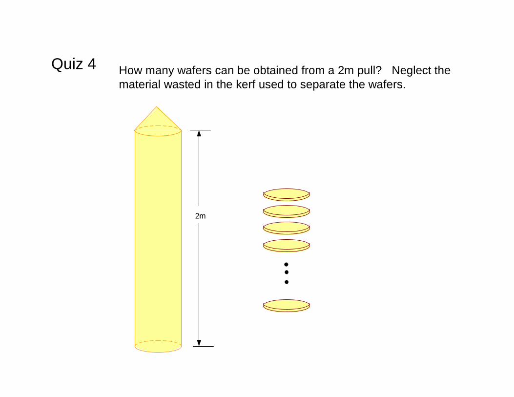
Quiz 4 How many wafers can be obtained from a 2m pull? Neglect the material wasted in the kerf used to separate the wafers.
2m

And the number is ….
6
31
2
45
7
8
9

And the number is ….
6
31
2
4
5
7
8
9
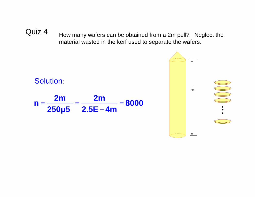
Quiz 4 How many wafers can be obtained from a 2m pull? Neglect the material wasted in the kerf used to separate the wafers.
2m
Solution:
80004m2.5E
2m250μ5
2mn =−
==
Review from last time:
Design rules specify minimum feature sizes and spacing
Often express rules in terms of a parameter λ
Critical to adhere to design rules but more conservative sizing and spacing not advisable
Design Rule Checker (DRC) widely used to verify design rules are satisfied
Wafers fabricated from large crystals of silicon
Crystalline structure of wafers is critical for proper device operation
Pull slow to maintain crystaline structure
Lightly doped (either n or p) during processing
Doping of wafer will be quite uniform (not graded impurity profile)

SCMOS Layout Rules - Well
Rule Description Lambda
SCMOS SUBM DEEP
1.1 Minimum width 10 12 12
1.2 Minimum spacing between wells at different potential 9 18 18
1.3 Minimum spacing between wells at same potential 6 6 6
1.4 Minimum spacing between wells of different type (if both are drawn) 0 0 0
Page 1 of 1SCMOS Layout Rules - Well
9/13/2004http://www.mosis.org/Technical/Designrules/scmos/scmos-well.html
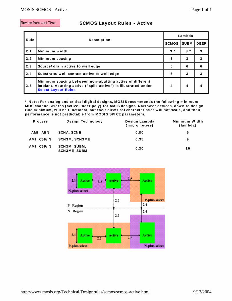
SCMOS Layout Rules - Active
Rule Description Lambda
SCMOS SUBM DEEP
2.1 Minimum width 3 * 3 * 3
2.2 Minimum spacing 3 3 3
2.3 Source/drain active to well edge 5 6 6
2.4 Substrate/well contact active to well edge 3 3 3
2.5 Minimum spacing between non-abutting active of different implant. Abutting active ("split-active") is illustrated under Select Layout Rules.
4 4 4
* Note: For analog and critical digital designs, MOSIS recommends the following minimum MOS channel widths (active under poly) for AMIS designs. Narrower devices, down to design rule minimum, will be functional, but their electrical characteristics will not scale, and their performance is not predictable from MOSIS SPICE parameters.
Process Design Technology Design Lambda (micrometers)
Minimum Width (lambda)
AMI_ABN SCNA, SCNE 0.80 5
AMI_C5F/N SCN3M, SCN3ME 0.35 9
AMI_C5F/N SCN3M_SUBM, SCN3ME_SUBM
0.30 10
Page 1 of 1MOSIS SCMOS - Active
9/13/2004http://www.mosis.org/Technical/Designrules/scmos/scmos-active.html
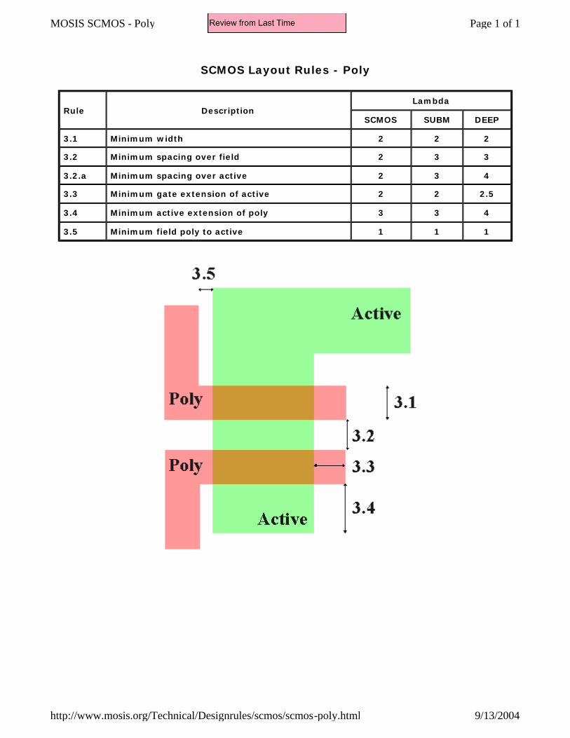
SCMOS Layout Rules - Poly
Rule Description Lambda
SCMOS SUBM DEEP
3.1 Minimum width 2 2 2
3.2 Minimum spacing over field 2 3 3
3.2.a Minimum spacing over active 2 3 4
3.3 Minimum gate extension of active 2 2 2.5
3.4 Minimum active extension of poly 3 3 4
3.5 Minimum field poly to active 1 1 1
Page 1 of 1MOSIS SCMOS - Poly
9/13/2004http://www.mosis.org/Technical/Designrules/scmos/scmos-poly.html
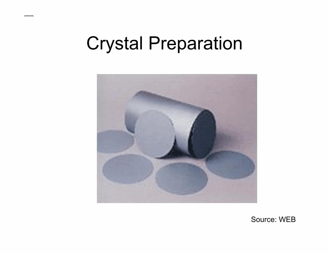
Crystal Preparation
Source: WEB

IC Fabrication Technology• Crystal Preparation• Masking• Photolithographic Process• Deposition• Etching• Diffusion• Oxidation• Epitaxy• Polysilicon• Contacts, Interconnect and Metalization• Planarization

Masking• Use masks or reticles to define features on a wafer
– Masks same size as wafer– Reticles used for projection– Reticle much smaller (but often termed mask)– Reticles often of quartz with chrome– Quality of reticle throughout life of use is critical– Single IC may require 20 or more reticles– Cost of “mask set” now exceeds $1million for state of the art
processes– Average usage 500 to 1500 times – Mask costs exceeding 50% of total fabrication costs in sub
100nm processes– Serve same purpose as a negative (or positive) in a
photographic process
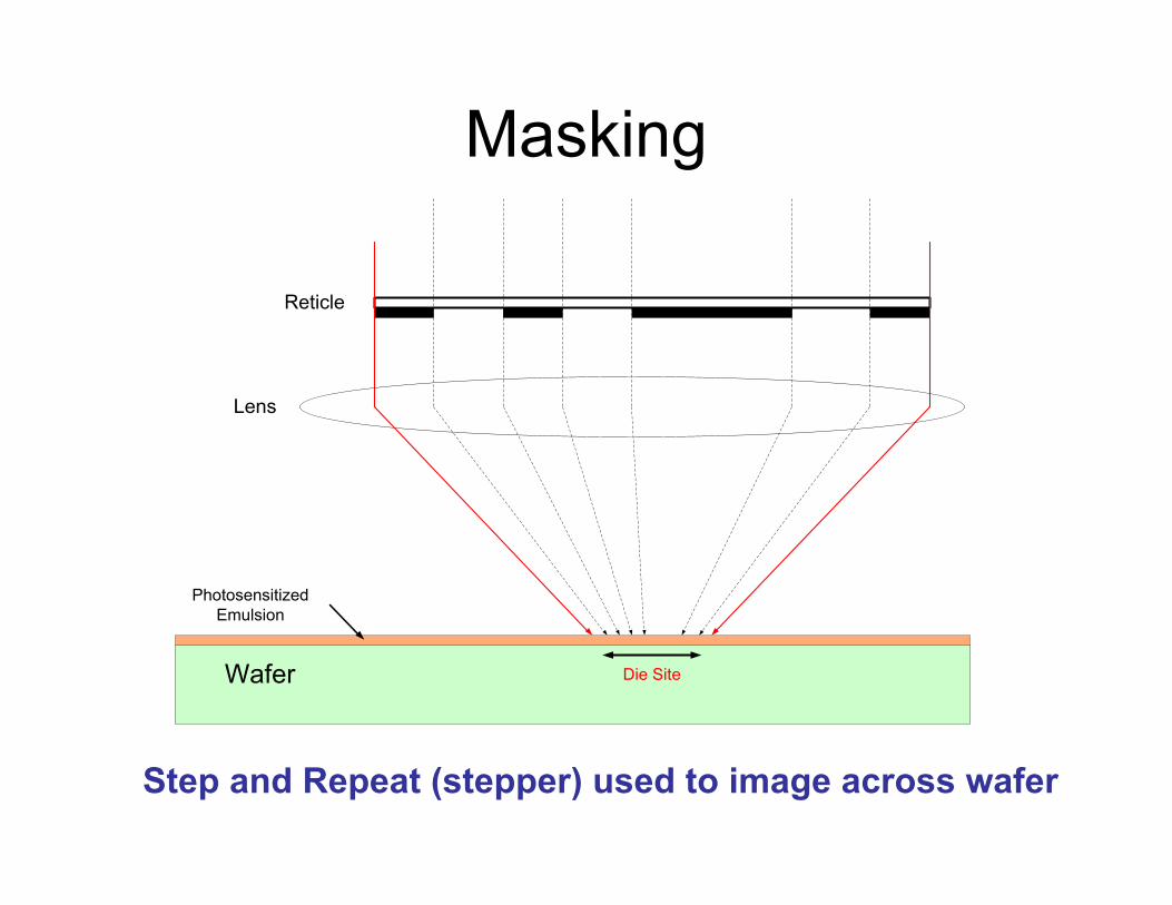
Masking
Lens
Reticle
Wafer
Photosensitized Emulsion
Die Site
Step and Repeat (stepper) used to image across wafer

MaskingExposure through reticle

Masking
Mask Features
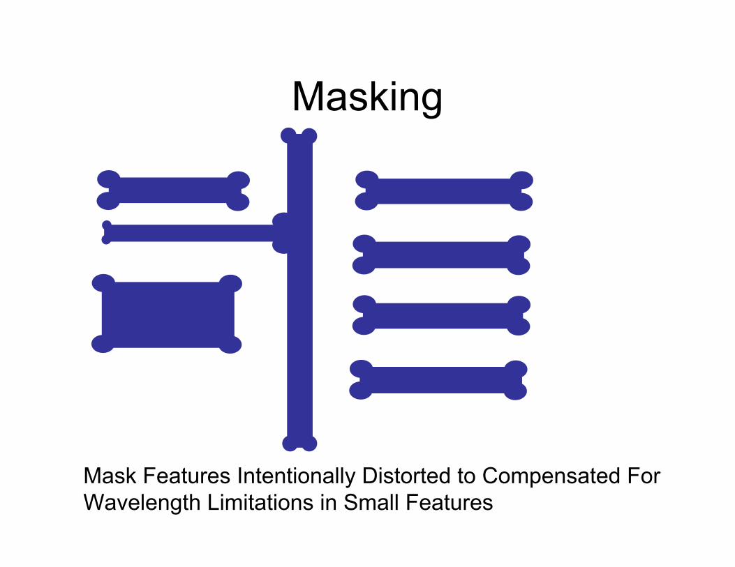
Masking
Mask Features Intentionally Distorted to Compensated For Wavelength Limitations in Small Features
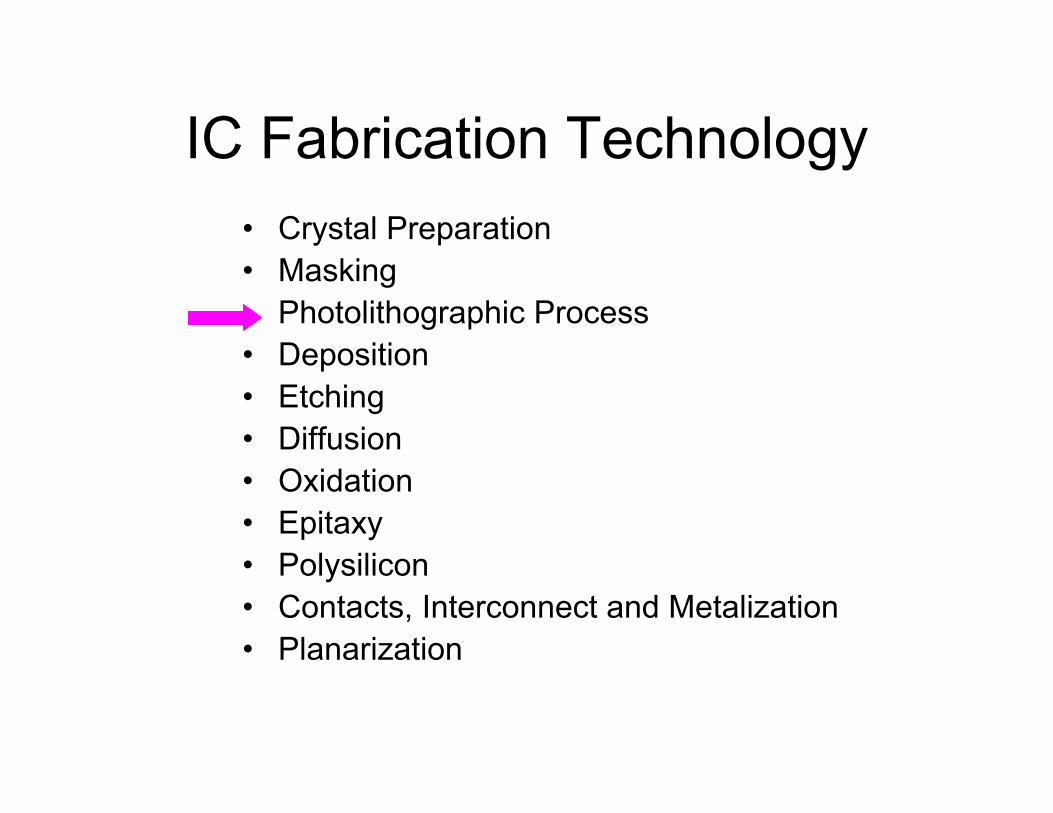
IC Fabrication Technology• Crystal Preparation• Masking• Photolithographic Process• Deposition• Etching• Diffusion• Oxidation• Epitaxy• Polysilicon• Contacts, Interconnect and Metalization• Planarization

Photolithographic Process• Photoresist
– Viscous Liquid– Uniform Application Critical (spinner)– Baked to harden– Approx 1u thick– Non-Selective– Types
• Negative – unexposed material removed when developed• Positive-exposed material removed when developed
• Exposure– Projection through reticle with stepper– Alignment is critical !!– E-Bean Exposures
• Eliminate need fro reticle• Capacity very small
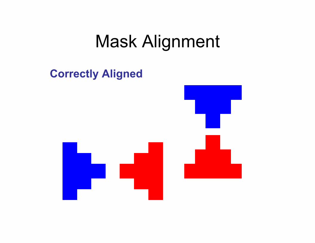
Mask Alignment
Correctly Aligned
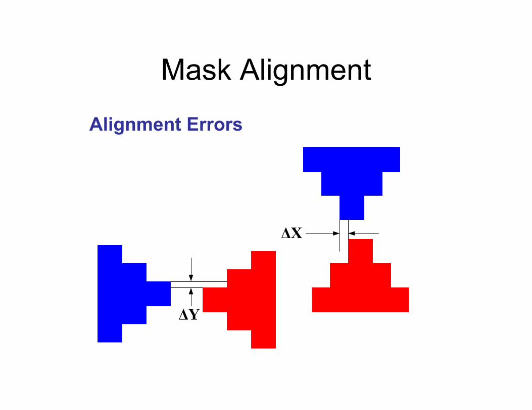
Mask Alignment
Alignment Errors
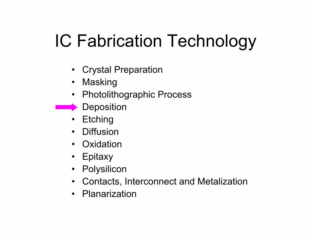
IC Fabrication Technology• Crystal Preparation• Masking• Photolithographic Process• Deposition• Etching• Diffusion• Oxidation• Epitaxy• Polysilicon• Contacts, Interconnect and Metalization• Planarization
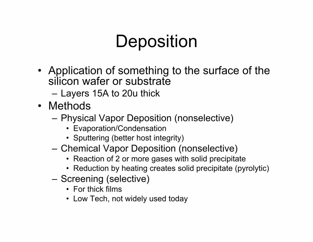
Deposition• Application of something to the surface of the
silicon wafer or substrate– Layers 15A to 20u thick
• Methods– Physical Vapor Deposition (nonselective)
• Evaporation/Condensation• Sputtering (better host integrity)
– Chemical Vapor Deposition (nonselective)• Reaction of 2 or more gases with solid precipitate• Reduction by heating creates solid precipitate (pyrolytic)
– Screening (selective)• For thick films• Low Tech, not widely used today

IC Fabrication Technology• Crystal Preparation• Masking• Photolithographic Process• Deposition• Etching• Diffusion• Oxidation• Epitaxy• Polysilicon• Contacts, Interconnect and Metalization• Planarization
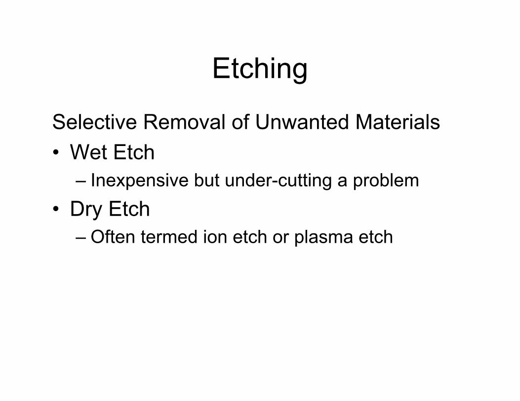
Etching
Selective Removal of Unwanted Materials• Wet Etch
– Inexpensive but under-cutting a problem• Dry Etch
– Often termed ion etch or plasma etch

Etching
Desired Physical Features
PhotoresistSiO2
p- Silicon
Note: Vertical Dimensions Generally Orders of Magnitude SmallerThan Lateral Dimensions so Different Vertical and Lateral ScalesWill be Used In This Discussion
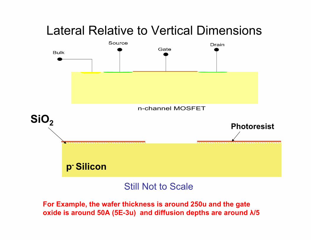
Lateral Relative to Vertical Dimensions
Still Not to Scale
PhotoresistSiO2
p- Silicon
For Example, the wafer thickness is around 250u and the gate oxide is around 50A (5E-3u) and diffusion depths are around λ/5
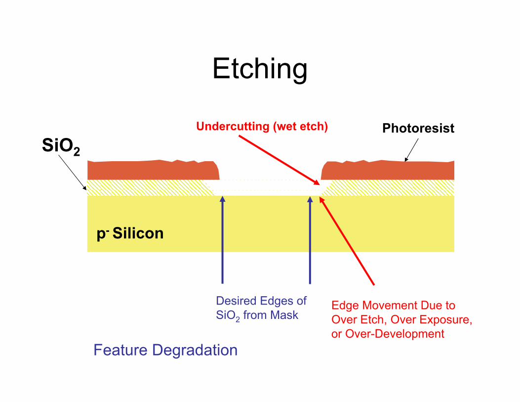
Etching
SiO2
PhotoresistUndercutting (wet etch)
Desired Edges of SiO2 from Mask
Feature Degradation
Edge Movement Due to Over Etch, Over Exposure, or Over-Development
p- Silicon

Etching
SiO2
Undercutting (wet etch)
Desired Edges of SiO2 from Mask
Edge Movement Due to Over Etch, Over Exposure, or Over-Development
SiO2 after photoresist removal
p- Silicon

End of Lecture 7