edc lab manual
DESCRIPTION
very goodTRANSCRIPT

BHARAT INSTITUTE OF ENGINEERING AND TECHNOLOGY DEPT.OF ECE EDC LAB MANUAL
1
1. BASIC ELECTRONIC COMPONENTS
1.1. COLOUR CODING OF RESISTOR
Colour Codes are used to identify the value of resistor. The numbers to the Colour are identified in the following sequence which is remembered as BBROY GREAT BRITAN VERY GOOD WIFE (BBROYGBVGW) and their assignment is listed in following table.
Black Brown Red Orange Yellow Green Blue Violet Grey White 0 1 2 3 4 5 6 7 8 9
Table1: Colour codes of resistor
First find the tolerance band, it will typically be gold (5%) and sometimes silver (10%). Starting from the other end, identify the first band - write down the number associated with that color Now read the next color, so write down its value next to the first value. Now read the third or 'multiplier exponent' band and write down that as the number of zeros. If the 'multiplier exponent' band is Gold move the decimal point one to the left. If the 'multiplier exponent' band is Silver move the decimal point two places to the left. If the resistor has one more band past the tolerance band it is a quality band.
Read the number as the '% Failure rate per 1000 hour' This is rated assuming full wattage being applied to the resistors. (To get better failure rates, resistors are typically specified to have twice the needed wattage dissipation that the circuit produces). Some resistors use this band for temco information. 1% resistors have three bands to read digits to the left of the multiplier. They have a different temperature coefficient in order to provide the 1% tolerance. At 1% the temperature coefficient starts to become an important factor. at +/-200 ppm a change in temperature of 25 Deg C causes a value change of up to 1%
Table2: procedure to find the value of resistor using Colour codes

BHARAT INSTITUTE OF ENGINEERING AND TECHNOLOGY DEPT.OF ECE EDC LAB MANUAL
2
1.2. COLOUR CODING OF CAPACITORS
An electrical device capable of storing electrical energy. In general, a capacitor consists of two metal plates insulated from each other by a dielectric. The capacitance of a capacitor depends primarily upon its shape and size and upon the relative permittivity εr of the medium between the plates. In vacuum, in air, and in most gases, εr ranges from one to several hundred.
One classification of capacitors comes from the physical state of their dielectrics, which may be gas (or vacuum), liquid, solid, or a combination of these. Each of these classifications may be subdivided according to the specific dielectric used. Capacitors may be further classified by their ability to be used in alternating-current (ac) or direct-current (dc) circuits with various current levels.
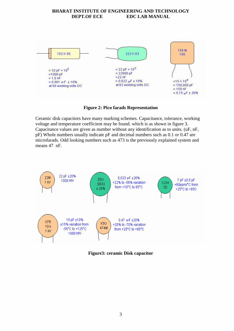
Capacitor Identification Codes: There are no international agreements in place to standardize capacitor identification. Most plastic film types (Figure1) have printed values and are normally in microfarads or if the symbol is n, Nan farads. Working voltage is easily identified. Tolerances are upper case letters: M = 20%, K = 10%, J = 5%, H = 2.5% and F = ± 1pF.
Figure 1: Plastic Film Types
A more difficult scheme is shown in Figure 2 where K is used for indicating Pico farads. The unit is Pico farads and the third number is a multiplier. A capacitor coded 474K63 means 47 × 10000 pF which is equivalent to 470000 pF or 0.47 microfarads. K indicates 10% tolerance. 50, 63 and 100 are working volts.
BHARAT INSTITUTE OF ENGINEERING AND TECHNOLOGY DEPT.OF ECE EDC LAB MANUAL
3
Figure 2: Pico farads Representation
Ceramic disk capacitors have many marking schemes. Capacitance, tolerance, working voltage and temperature coefficient may be found. which is as shown in figure 3. Capacitance values are given as number without any identification as to units. (uF, nF, pF) Whole numbers usually indicate pF and decimal numbers such as 0.1 or 0.47 are microfarads. Odd looking numbers such as 473 is the previously explained system and means 47 nF.
Figure3: ceramic Disk capacitor

BHARAT INSTITUTE OF ENGINEERING AND TECHNOLOGY DEPT.OF ECE EDC LAB MANUAL
4
Figure 4 shows some other miscellaneous schemes.
Figure 4: miscellaneous schemes.
Electrolytic capacitor properties There are a number of parameters of importance beyond the basic capacitance and capacitive reactance when using electrolytic capacitors. When designing circuits using electrolytic capacitors it is necessary to take these additional parameters into consideration for some designs, and to be aware of them when using electrolytic capacitors
• ESR Equivalent series resistance: Electrolytic capacitors are often used in circuits where current levels are relatively high. Also under some circumstances and current sourced from them needs to have low source impedance, for example when the capacitor is being used in a power supply circuit as a reservoir capacitor. Under these conditions it is necessary to consult the manufacturers’ datasheets to discover whether the electrolytic capacitor chosen will meet the requirements for the circuit. If the ESR is high, then it will not be able to deliver the required amount of current in the circuit, without a voltage drop resulting from the ESR which will be seen as a source resistance.
• Frequency response: One of the problems with electrolytic capacitors is that they have a limited frequency response. It is found that their ESR rises with frequency and this generally limits their use to frequencies below about 100 kHz. This is particularly true for large capacitors, and even the smaller electrolytic capacitors should not be relied upon at high frequencies. To gain exact details it is necessary to consult the manufacturer’s data for a given part.
• Leakage: Although electrolytic capacitors have much higher levels of capacitance for a given volume than most other capacitor technologies, they can also have a higher level of leakage. This is not a problem for most applications, such as when they are used in power supplies. However under some circumstances they are not suitable. For example they should not be used around the input circuitry of an operational amplifier. Here even a small amount of leakage can cause problems because of the high input impedance levels of the op-amp. It is also worth noting that the levels of leakage are considerably higher in the reverse direction.

BHARAT INSTITUTE OF ENGINEERING AND TECHNOLOGY DEPT.OF ECE EDC LAB MANUAL
5
• Ripple current: When using electrolytic capacitors in high current applications such as the reservoir capacitor of a power supply, it is necessary to consider the ripple current it is likely to experience. Capacitors have a maximum ripple current they can supply. Above this they can become too hot which will reduce their life. In extreme cases it can cause the capacitor to fail. Accordingly it is necessary to calculate the expected ripple current and check that it is within the manufacturer’s maximum ratings.
• Tolerance: Electrolytic capacitors have a very wide tolerance. Typically this may be -50% + 100%. This is not normally a problem in applications such as decoupling or power supply smoothing, etc. However they should not be used in circuits where the exact value is of importance.
• Polarization: Unlike many other types of capacitor, electrolytic capacitors are polarized and must be connected within a circuit so that they only see a voltage across them in a particular way.
The physical appearance of electrolytic capacitor is as shown in Figure 5.The capacitors themselves are marked so that polarity can easily be seen. In addition to this it is common for the can of the capacitor to be connected to the negative terminal.
Figure 5: Electrolytic capacitor
It is absolutely necessary to ensure that any electrolytic capacitors are connected within a circuit with the correct polarity. A reverse bias voltage will cause the centre oxide layer forming the dielectric to be destroyed as a result of electrochemical reduction. If this occurs a short circuit will appear and excessive current can cause the capacitor to become very hot. If this occurs the component may leak the electrolyte, but under some circumstances they can explode. As this is not uncommon, it is very wise to take precautions and ensure the capacitor is fitted correctly, especially in applications where high current capability exists.
1.3. COLOUR CODING OF INDUCTORS
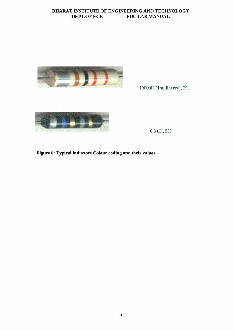
Inductor is just coil wound which provides more reactance for high frequencies and low reactance for low frequencies. Molded inductors follow the same scheme except the units are usually micro henries. A brown-black-red inductor is most likely a 1000 uH. Sometimes a silver or gold band is used as a decimal point. So a red-gold-violet inductor would be a 2.7 uH. Also expect to see a wide silver or gold band before the first value band and a thin tolerance band at the end. The typical Colour codes and their values are shown in Figure 6.
BHARAT INSTITUTE OF ENGINEERING AND TECHNOLOGY DEPT.OF ECE EDC LAB MANUAL
6
1000uH (1millihenry), 2%
6.8 uH, 5%
Figure 6: Typical inductors Colour coding and their values.

BHARAT INSTITUTE OF ENGINEERING AND TECHNOLOGY DEPT.OF ECE EDC LAB MANUAL
7
2. CIRCUIT SYMBOLS
WIRES AND CONNECTIONS
S.No. COMPONENT
NAME CIRCUIT SYMBOL FUNCTION
1 WIRE
To pass current very easily from one part of a circuit to another.
2 WIRES JOINED
A 'blob' should be drawn where wires are connected (joined), but it is sometimes omitted. Wires connected at 'crossroads' should be staggered slightly to form two T-junctions, as shown on the right.
3 WIRES NOT JOINED
In complex diagrams it is often necessary to draw wires crossing even though they are not connected. I prefer the 'bridge' symbol shown on the right because the simple crossing on the left may be misread as a join where you have forgotten to add a 'blob'.
POWER SUPPLIES
S.No COMPONENT
NAME CIRCUIT SYMBOL FUNCTION
1. CELL
Supplies electrical energy.The larger terminal (on the left) is positive (+). A single cell is often called a battery, but strictly a battery is two or more cells joined together

BHARAT INSTITUTE OF ENGINEERING AND TECHNOLOGY DEPT.OF ECE EDC LAB MANUAL
8
2. BATTERY
Supplies electrical energy. A battery is more than one cell. The larger terminal (on the left) is positive (+).
3. DC SUPPLY
Supplies electrical energy. DC = Direct Current, always flowing in one direction.
4. AC SUPPLY
Supplies electrical energy. AC = Alternating Current, continually changing direction.
5. FUSE
A safety device which will 'blow' (melt) if the current flowing through it exceeds a specified value.
6. TRANSFORMER
Two coils of wire linked by an iron core. Transformers are used to step up (increase) and step down (decrease) AC voltages. Energy is transferred between the coils by the magnetic field in the core. There is no electrical connection between the coils.
7. EARTH(GROUND)
A connection to earth. For many electronic circuits this is the 0V (zero volts) of the power supply, but for mains electricity and some radio circuits it really means the earth. It is also known as ground.
OUTPUT DEVICES: LAMPS, HEATER, MOTOR, ETC.
S.NO COMPONENT
NAME CIRCUIT SYMBOL FUNCTION
1. LAMP(LIGHTING)
A transducer which converts electrical energy to light. This symbol is

BHARAT INSTITUTE OF ENGINEERING AND TECHNOLOGY DEPT.OF ECE EDC LAB MANUAL
9
used for a lamp providing illumination, for example a car headlamp or torch bulb
2. LAMP(INDICATOR)
A transducer which converts electrical energy to light. This symbol is used for a lamp which is an indicator, for example a warning light on a car dashboard.
3. HEATER
A transducer which converts electrical energy to heat.
4. MOTOR
A transducer which converts electrical energy to kinetic energy (motion).
5. BELL
A transducer which converts electrical energy to sound.
6. BUZZER
A transducer which converts electrical energy to sound.
7. INDUCTOR(SOLINOID,COIL)
A coil of wire which creates a magnetic field when current passes through it. It may have an iron core inside the coil. It can be used as a transducer converting electrical energy to mechanical energy by pulling on something.
SWITCHES
S.NO COMPONENT
NAME CIRCUIT SYMBOL FUNCTION
1. PUSH SWITCH(PUSH TO MAKE)
A push switch allows current to flow only when the button is pressed. This is the switch used to operate a doorbell.
BHARAT INSTITUTE OF ENGINEERING AND TECHNOLOGY DEPT.OF ECE EDC LAB MANUAL
10
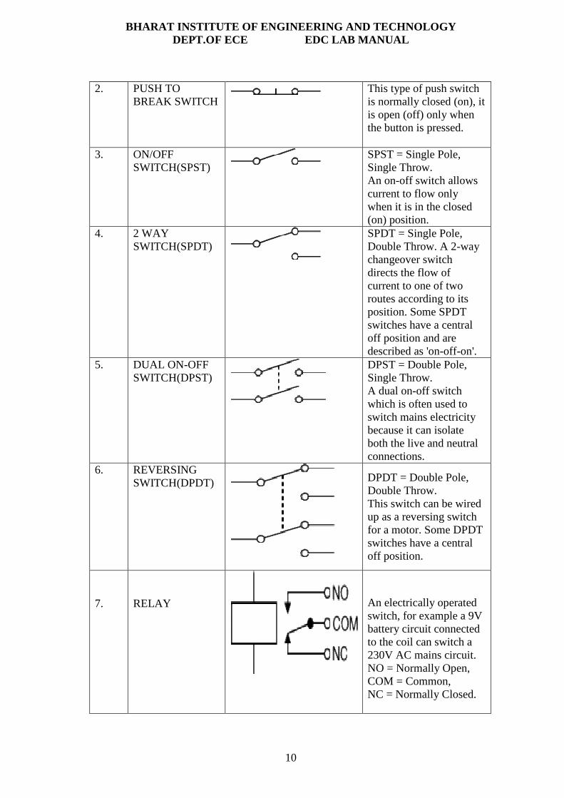
2. PUSH TO BREAK SWITCH
This type of push switch is normally closed (on), it is open (off) only when the button is pressed.
3. ON/OFF SWITCH(SPST)
SPST = Single Pole, Single Throw. An on-off switch allows current to flow only when it is in the closed (on) position.
4. 2 WAY SWITCH(SPDT)
SPDT = Single Pole, Double Throw. A 2-way changeover switch directs the flow of current to one of two routes according to its position. Some SPDT switches have a central off position and are described as 'on-off-on'.
5. DUAL ON-OFF SWITCH(DPST)
DPST = Double Pole, Single Throw. A dual on-off switch which is often used to switch mains electricity because it can isolate both the live and neutral connections.
6. REVERSING SWITCH(DPDT)
DPDT = Double Pole, Double Throw. This switch can be wired up as a reversing switch for a motor. Some DPDT switches have a central off position.
7.
RELAY
An electrically operated switch, for example a 9V battery circuit connected to the coil can switch a 230V AC mains circuit. NO = Normally Open, COM = Common, NC = Normally Closed.

BHARAT INSTITUTE OF ENGINEERING AND TECHNOLOGY DEPT.OF ECE EDC LAB MANUAL
11
RESISTORS
S.NO COMPONENT
NAME CIRCUIT SYMBOL FUNCTION
1. RESISTOR
Or
A resistor restricts the flow of current, for example to limit the current passing through an LED. A resistor is used with a capacitor in a timing circuit.
2.
VARIABLE RESISTOR(RHEOSTAT)
This type of variable resistor with 2 contacts (a rheostat) is usually used to control current. Examples include: adjusting lamp brightness, adjusting motor speed, and adjusting the rate of flow of charge into a capacitor in a timing circuit.
3. VARIABLE RESISTOR(POTENTIOMETER)
This type of variable resistor with 3 contacts (a potentiometer) is usually used to control voltage. It can be used like this as a transducer converting position (angle of the control spindle) to an electrical signal
4. VARIABLE RESISTER(PRESET)
This type of variable resistor (a preset) is operated with a small screwdriver or similar tool. It is designed to be set when the circuit is made and then left without further adjustment. Presets are cheaper than normal variable resistors so they are often used in projects to reduce the cost

BHARAT INSTITUTE OF ENGINEERING AND TECHNOLOGY DEPT.OF ECE EDC LAB MANUAL
12
CAPACITORS
S.NO NAME OF THE
COMPONENT CIRCUIT SYMBOL FUNCTION OF THE
COMPONENT 1. CAPACITOR
A capacitor stores electric charge. A capacitor is used with a resistor in a timing circuit. It can also be used as a filter, to block DC signals but pass AC signals.
2.
CAPACITOR POLARISED
A capacitor stores electric charge. This
type must be connected the correct way round.
A capacitor is used with a resistor in a
timing circuit. It can also be used as a filter, to block DC signals but
pass AC signals. 3.
VARIABLE CAPACITOR
A variable capacitor is used in a radio tuner.
3.
TRIMMER CAPACITOR
This type of variable capacitor (a trimmer) is operated with a small screwdriver or similar tool. It is designed to be set when the circuit is made and then left without further adjustment
DIODES
S.NO NAME OF THE COMPONENT
CIRCUIT SYMBOL FUNCTION OF THE COMPONENT
1. DIODE
A device which only allows current to flow in one direction
2. LED(LIGHT EMITTING
DIODE)
A transducer which converts electrical energy to light.

BHARAT INSTITUTE OF ENGINEERING AND TECHNOLOGY DEPT.OF ECE EDC LAB MANUAL
13
3.
ZENER DIODE
A special diode which is used to maintain a fixed voltage across its terminals
4. Photodiode
A light-sensitive diode.
TRANSISTORS
S.NO NAME OF THE
COMPONENT CIRCUIT SYMBOL FUNCTION OF THE
COMPONENT 5.
TRANSISTOR NPN
A transistor amplifies current. It can be used with other components to make an amplifier or switching circuit.
6.
TRANSISTOR PNP
A transistor amplifies current. It can be used with other components to make an amplifier or switching circuit.
7.
PHOTO TRANSISTOR
A light-sensitive transistor.
AUDIO AND RADIO DEVICES
S.NO NAME OF THE
COMPONENT CIRCUIT SYMBOL FUNCTION OF THE
COMPONENT 1.
MICROPHONE
A transducer which converts sound to electrical energy.
2.
EARPHONE
A transducer which converts electrical energy to sound.
BHARAT INSTITUTE OF ENGINEERING AND TECHNOLOGY DEPT.OF ECE EDC LAB MANUAL
14
3.
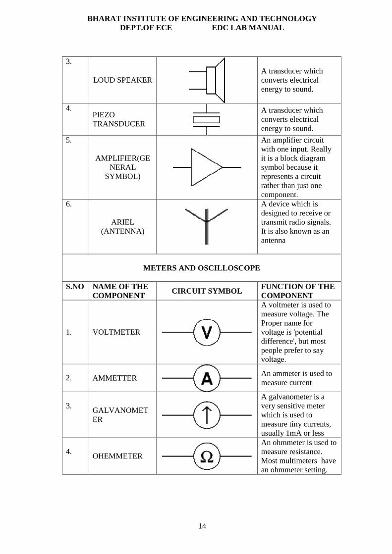
LOUD SPEAKER
A transducer which converts electrical energy to sound.
4. PIEZO TRANSDUCER
A transducer which converts electrical energy to sound.
5.
AMPLIFIER(GENERAL
SYMBOL)
An amplifier circuit with one input. Really it is a block diagram symbol because it represents a circuit rather than just one component.
6.
ARIEL (ANTENNA)
A device which is designed to receive or transmit radio signals. It is also known as an antenna
METERS AND OSCILLOSCOPE
S.NO NAME OF THE
COMPONENT CIRCUIT SYMBOL FUNCTION OF THE
COMPONENT 1. VOLTMETER
A voltmeter is used to measure voltage. The Proper name for voltage is 'potential difference', but most people prefer to say voltage.
2. AMMETTER
An ammeter is used to measure current
3.
GALVANOMETER
A galvanometer is a very sensitive meter which is used to measure tiny currents, usually 1mA or less
4.
OHEMMETER
An ohmmeter is used to measure resistance. Most multimeters have an ohmmeter setting.

BHARAT INSTITUTE OF ENGINEERING AND TECHNOLOGY DEPT.OF ECE EDC LAB MANUAL
15
5.
OSCILLOSCOPE
An oscilloscope is used to display the shape of electrical signals and it can be used to measure their voltage and time period.
SENSORS (INPUT DEVICES)
S.NO NAME OF THE
COMPONENT CIRCUIT SYMBOL FUNCTION OF THE
COMPONENT 1. LDR
A transducer which converts brightness (light) to resistance (an electrical property). LDR = Light Dependent Resistor
2.
THERMISTOR
A transducer which converts temperature (heat) to resistance (an electrical property).

BHARAT INSTITUTE OF ENGINEERING AND TECHNOLOGY DEPT.OF ECE EDC LAB MANUAL
16
3. STUDY OF CRO
An oscilloscope is a test instrument which allows us to look at the 'shape' of electrical signals by displaying a graph of voltage against time on its screen. It is like a voltmeter with the valuable extra function of showing how the voltage varies with time. A graticule with a 1cm grid enables us to take measurements of voltage and time from the screen.
The graph, usually called the trace, is drawn by a beam of electrons striking the phosphor coating of the screen making it emit light, usually green or blue. This is similar to the way a television picture is produced.
Oscilloscopes contain a vacuum tube with a cathode (negative electrode) at one end to emit electrons and an anode (positive electrode) to accelerate them so they move rapidly down the tube to the screen. This arrangement is called an electron gun. The tube also contains electrodes to deflect the electron beam up/down and left/right.
The electrons are called cathode rays because they are emitted by the cathode and this gives the oscilloscope its full name of cathode ray oscilloscope or CRO.
A dual trace oscilloscope can display two traces on the screen, allowing us to easily compare the input and output of an amplifier for example. It is well worth paying the modest extra cost to have this facility.
Figure1: Front Panel of CRO

BHARAT INSTITUTE OF ENGINEERING AND TECHNOLOGY DEPT.OF ECE EDC LAB MANUAL
17
BASIC OPERATION:
Figure2: Internal Blocks of CRO
Setting up an oscilloscope: Oscilloscopes are complex instruments with many controls and they require some care to set up and use successfully. It is quite easy to 'lose' the trace off the screen if controls are set wrongly.
There is some variation in the arrangement and labeling of the many controls so the following instructions may need to be adapted for this instrument.
1. Switch on the oscilloscope to warm up (it takes a minute or two). 2. Do not connect the input lead at this stage. 3. Set the AC/GND/DC switch (by the Y INPUT) to DC. 4. Set the SWP/X-Y switch to SWP (sweep). 5. Set Trigger Level to AUTO. 6. Set Trigger Source to INT (internal, the y input). 7. Set the Y AMPLIFIER to 5V/cm (a moderate value). 8. Set the TIMEBASE to 10ms/cm (a moderate speed). 9. Turn the time base VARIABLE control to 1 or CAL. 10. Adjust Y SHIFT (up/down) and X SHIFT (left/right) to give a trace across the
middle of the screen, like the picture. 11. Adjust INTENSITY (brightness) and FOCUS to give a bright, sharp trace.
fluorescent screen
Y plates
X plates
electron gun
anode
cathode
Electron beam

BHARAT INSTITUTE OF ENGINEERING AND TECHNOLOGY DEPT.OF ECE EDC LAB MANUAL
18
The following type of trace is observed on CRO after setting up, when there is no input signal connected.
Figure 3: Absence of input signal
Connecting an oscilloscope: The Y INPUT lead to an oscilloscope should be a co-axial lead and the figure 4 shows its construction. The central wire carries the signal and the screen is connected to earth (0V) to shield the signal from electrical interference (usually called noise).
Figure 4: Construction of a co-axial lead
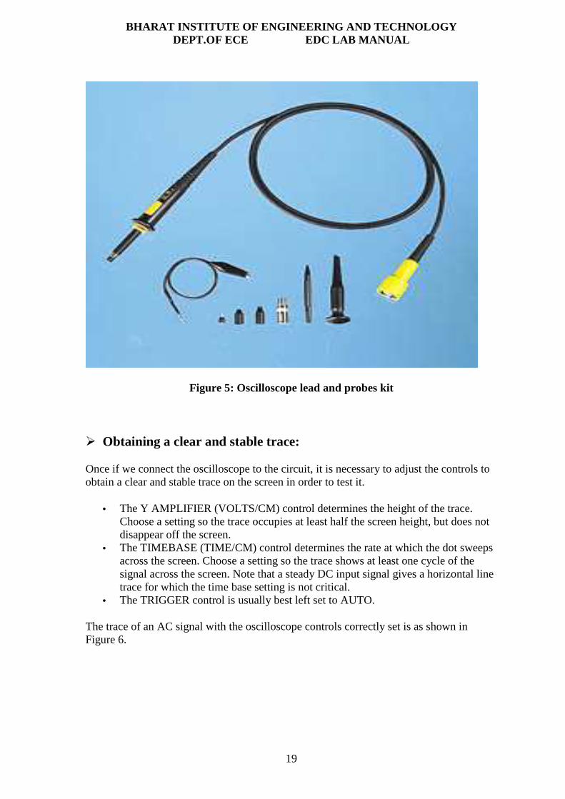
Most oscilloscopes have a BNC socket for the y input and the lead is connected with a push and twist action, to disconnect we need to twist and pull. Professionals use a specially designed lead and probes kit for best results with high frequency signals and when testing high resistance circuits, but this is not essential for simpler work at audio frequencies (up to 20 kHz).
BHARAT INSTITUTE OF ENGINEERING AND TECHNOLOGY DEPT.OF ECE EDC LAB MANUAL
19
Figure 5: Oscilloscope lead and probes kit
Obtaining a clear and stable trace:
Once if we connect the oscilloscope to the circuit, it is necessary to adjust the controls to obtain a clear and stable trace on the screen in order to test it.
• The Y AMPLIFIER (VOLTS/CM) control determines the height of the trace. Choose a setting so the trace occupies at least half the screen height, but does not disappear off the screen.
• The TIMEBASE (TIME/CM) control determines the rate at which the dot sweeps across the screen. Choose a setting so the trace shows at least one cycle of the signal across the screen. Note that a steady DC input signal gives a horizontal line trace for which the time base setting is not critical.
• The TRIGGER control is usually best left set to AUTO.
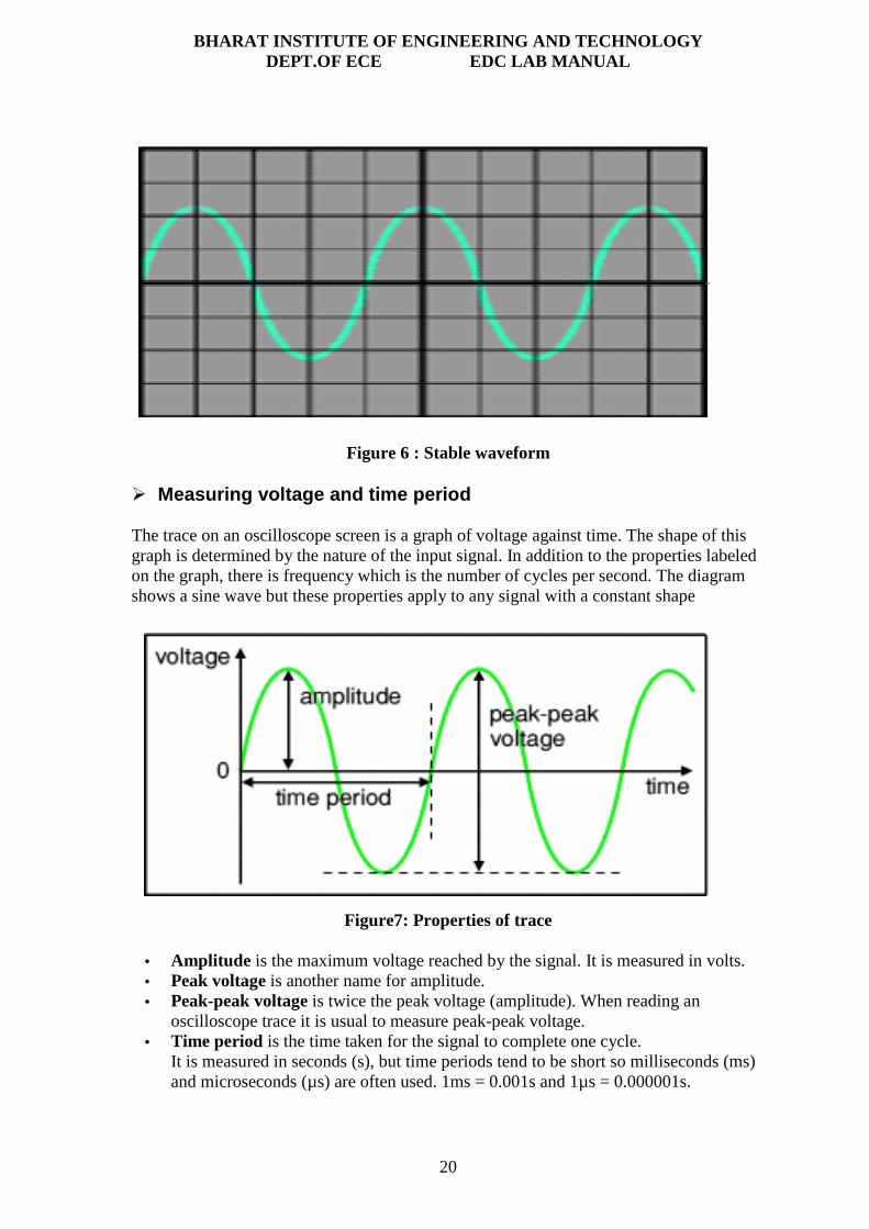
The trace of an AC signal with the oscilloscope controls correctly set is as shown in Figure 6.
BHARAT INSTITUTE OF ENGINEERING AND TECHNOLOGY DEPT.OF ECE EDC LAB MANUAL
20
Figure 6 : Stable waveform
Measuring voltage and time period The trace on an oscilloscope screen is a graph of voltage against time. The shape of this graph is determined by the nature of the input signal. In addition to the properties labeled on the graph, there is frequency which is the number of cycles per second. The diagram shows a sine wave but these properties apply to any signal with a constant shape
Figure7: Properties of trace
• Amplitude is the maximum voltage reached by the signal. It is measured in volts. • Peak voltage is another name for amplitude. • Peak-peak voltage is twice the peak voltage (amplitude). When reading an
oscilloscope trace it is usual to measure peak-peak voltage. • Time period is the time taken for the signal to complete one cycle.
It is measured in seconds (s), but time periods tend to be short so milliseconds (ms) and microseconds (µs) are often used. 1ms = 0.001s and 1µs = 0.000001s.

BHARAT INSTITUTE OF ENGINEERING AND TECHNOLOGY DEPT.OF ECE EDC LAB MANUAL
21
• Frequency is the number of cycles per second. It is measured in hertz (Hz), but frequencies tend to be high so kilohertz (kHz) and megahertz (MHz) are often used. 1kHz = 1000Hz and 1MHz = 1000000Hz.
Frequency = 1 Time period
Time period = 1 Frequency
A) Voltage: Voltage is shown on the vertical y-axis and the scale is determined by the Y AMPLIFIER (VOLTS/CM) control. Usually peak-peak voltage is measured because it can be read correctly even if the position of 0V is not known. The amplitude is half the peak-peak voltage.
Voltage = distance in cm × volts/cm
B) Time period: Time is shown on the horizontal x-axis and the scale is determined by the TIMEBASE (TIME/CM) control. The time period (often just called period) is the time for one cycle of the signal. The frequency is the number of cycles per second, frequency = 1/time period.
Time = distance in cm × time/cm
BHARAT INSTITUTE OF ENGINEERING AND TECHNOLOGY DEPT.OF ECE EDC LAB MANUAL
22
4. STUDY OF FUNCTION GENERATOR
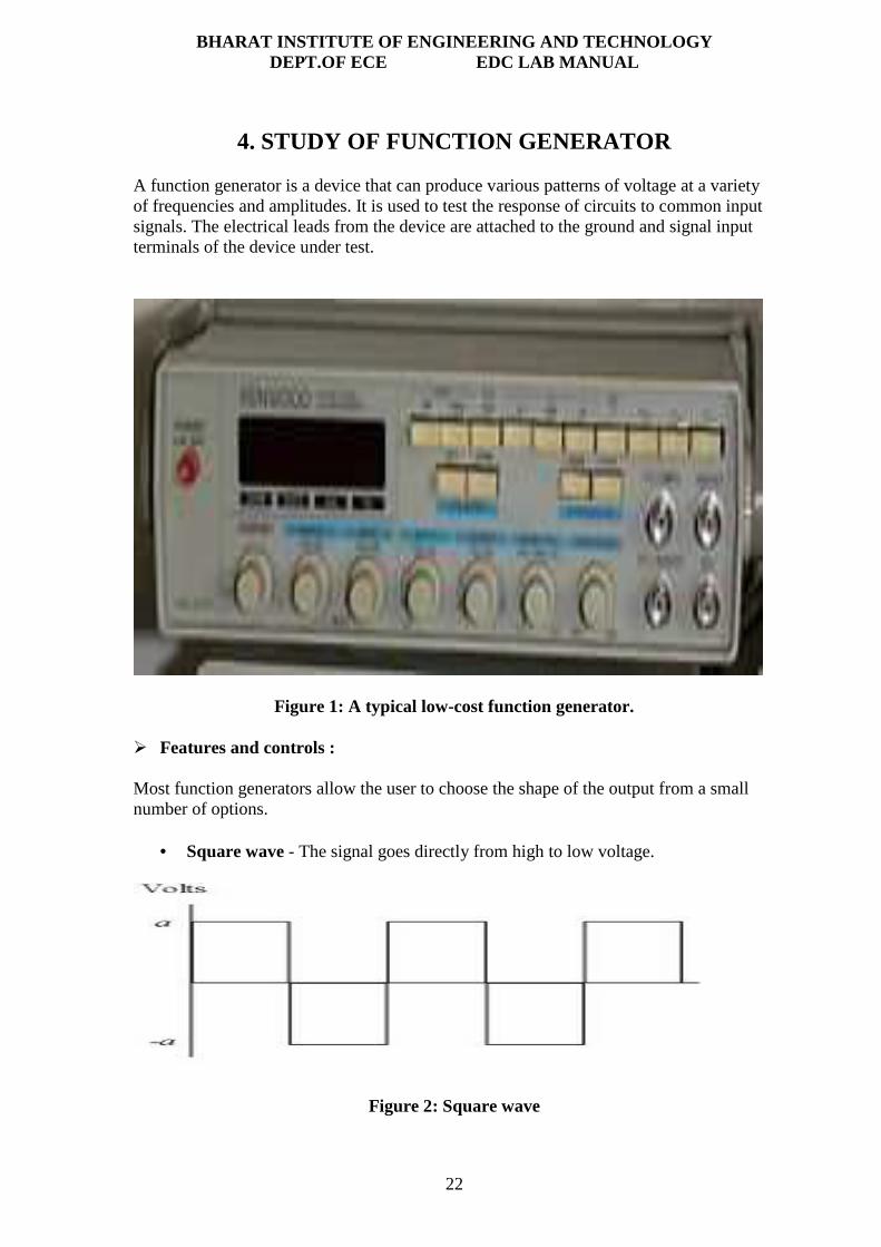
A function generator is a device that can produce various patterns of voltage at a variety of frequencies and amplitudes. It is used to test the response of circuits to common input signals. The electrical leads from the device are attached to the ground and signal input terminals of the device under test.
Figure 1: A typical low-cost function generator.
Features and controls :
Most function generators allow the user to choose the shape of the output from a small number of options.
• Square wave - The signal goes directly from high to low voltage.
Figure 2: Square wave

BHARAT INSTITUTE OF ENGINEERING AND TECHNOLOGY DEPT.OF ECE EDC LAB MANUAL
23
The duty cycle of a signal refers to the ratio of high voltage to low voltage time in a square wave signal.
• Sine wave - The signal curves like a sinusoid from high to low voltage.
Figure3 : Sine Wave
• Triangle wave - The signal goes from high to low voltage at a fixed rate.
Figure4: Triangular Wave

BHARAT INSTITUTE OF ENGINEERING AND TECHNOLOGY DEPT.OF ECE EDC LAB MANUAL
24
The amplitude control on a function generator varies the voltage difference between the high and low voltage of the output signal. The direct current (DC) offset control on a function generator varies the average voltage of a signal relative to the ground.
The frequency control of a function generator controls the rate at which output signal oscillates. On some function generators, the frequency control is a combination of different controls. One set of controls chooses the broad frequency range (order of magnitude) and the other selects the precise frequency. This allows the function generator to handle the enormous variation in frequency scale needed for signals.
How to use a function generator:
After powering on the function generator, the output signal needs to be configured to the desired shape. Typically, this means connecting the signal and ground leads to an oscilloscope to check the controls. Adjust the function generator until the output signal is correct, then attach the signal and ground leads from the function generator to the input and ground of the device under test. For some applications, the negative lead of the function generator should attach to a negative input of the device, but usually attaching to ground is sufficient.

BHARAT INSTITUTE OF ENGINEERING AND TECHNOLOGY DEPT.OF ECE EDC LAB MANUAL
25
5. STUDY OF REGULATED POWER SUPPLY
There are many types of power supply. Most are designed to convert high voltage AC mains electricity to a suitable low voltage supply for electronic circuits and other devices. A power supply can by broken down into a series of blocks, each of which performs a particular function. For example a 5V regulated supply:
Figure1: Block Diagram of Regulated power supply
Each of the blocks is described in more detail below:
• Transformer: Steps down high voltage AC mains to low voltage AC. • Rectifier: Converts AC to DC, but the DC output is varying. • Smoothing: Smooths the DC from varying greatly to a small ripple. • Regulator: Eliminates ripple by setting DC output to a fixed voltage.
Dual Supplies: Some electronic circuits require a power supply with positive and negative outputs as well as zero volts (0V). This is called a 'dual supply' because it is like two ordinary supplies connected together as shown in the diagram. Dual supplies have three outputs, for example a ±9V supply has +9V, 0V and -9V outputs.
Figure 2: Dual Supply

BHARAT INSTITUTE OF ENGINEERING AND TECHNOLOGY DEPT.OF ECE EDC LAB MANUAL
26
6. TYPES OF CIRCUIT BOARDS
• Breadboard: This is a way of making a temporary circuit, for testing purposes or to try out an idea. No soldering is required and all the components can be re-used afterwards. It is easy to change connections and replace components. Almost all the Electronics Club projects started life on a breadboard to check that the circuit worked as intended. The following figure depicts the appearance of Bread board in which the holes in top and bottom stribes are connected horizontally that are used for power supply and ground connection conventionally and holes on middle stribes connected vertically. And that are used for circuit connections conventionally.
Figure 1: Bread board
• Strip board: Strip board has parallel strips of copper track on one side. The strips are 0.1" (2.54mm) apart and there are holes every 0.1" (2.54mm). Stripboard requires no special preparation other than cutting to size. It can be cut with a junior hacksaw, or simply snap it along the lines of holes by putting it over the edge of a bench or table and pushing hard.
Figure 2: Strip board

BHARAT INSTITUTE OF ENGINEERING AND TECHNOLOGY DEPT.OF ECE EDC LAB MANUAL
27
• Printed Circuit Board:
A printed circuit board, or PCB, is used to mechanically support and electrically connect electronic components using conductive pathways, tracks or traces etched from copper sheets laminated onto a non-conductive substrate. It is also referred to as printed wiring board (PWB) or etched wiring board. A PCB populated with electronic components is a printed circuit assembly (PCA), also known as a printed circuit board assembly (PCBA).
Printed circuit boards have copper tracks connecting the holes where the components are placed. They are designed specially for each circuit and make construction very easy. However, producing the PCB requires special equipment so this method is not recommended if you are a beginner unless the PCB is provided for you.
Figure 3: Printed circuit board
PCBs are inexpensive, and can be highly reliable. They require much more layout effort and higher initial cost than either wire-wrapped or point-to-point constructed circuits, but are much cheaper and faster for high-volume production. Much of the electronics industry's PCB design, assembly, and quality control needs are set by standards that are published by the IPC organization.

BHARAT INSTITUTE OF ENGINEERING AND TECHNOLOGY DEPT.OF ECE EDC LAB MANUAL
28
EXP.NO: 1
P-N JUNCTION DIODE CHARACTERISTICS
AIM: 1. To observe and draw the Forward and Reverse bias V-I Characteristics of a P-N Junction diode.
2. To calculate static and dynamic resistance in both forward and Reverse Bias conditions.
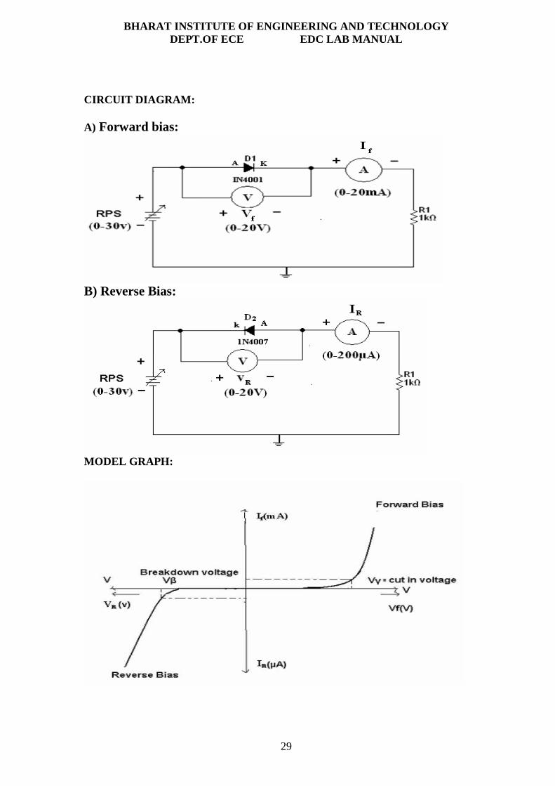
APPARATUS: 1. P-N Diode IN4007 - 1No. 2. Regulated Power supply (0-30V) - 1No. 3. Resistor 1KΩ - 1No. 4. Ammeter (0-20 mA) - 1No 5. Ammeter (0-200µA) - 1No. 6. Voltmeter (0-20V) - 2No. 7. Bread board 8. Connecting wires THEORY: A p-n junction diode conducts only in one direction. The V-I characteristics of the diode are curve between voltage across the diode and current flowing through the diode. When external voltage is zero, circuit is open and the potential barrier does not allow the current to flow. Therefore, the circuit current is zero. When P-type (Anode) is connected to Positive terminal and n- type (cathode) is connected to Negative terminal of the supply voltage is known as forward bias. The potential barrier is reduced when diode is in the forward biased condition. At some forward voltage, the potential barrier altogether eliminated and current starts flowing through the diode and also in the circuit. Then diode is said to be in ON state. The current increases with increasing forward voltage.
When N-type (cathode) is connected to Positive terminal and P-type (Anode) is connected to Negative terminal of the supply voltage is known as reverse bias and the potential barrier across the junction increases. Therefore, the junction resistance becomes very high and a very small current (reverse saturation current) flows in the circuit. Then diode is said to be in OFF state. The reverse bias current is due to minority charge carriers.
BHARAT INSTITUTE OF ENGINEERING AND TECHNOLOGY DEPT.OF ECE EDC LAB MANUAL
29
CIRCUIT DIAGRAM: A) Forward bias:
B) Reverse Bias:
MODEL GRAPH:

BHARAT INSTITUTE OF ENGINEERING AND TECHNOLOGY DEPT.OF ECE EDC LAB MANUAL
30
PROCEDURE:
A) FORWARD BIAS:
1. Connections are made as per the circuit diagram. 2. For forward bias, the RPS +ve is connected to the anode of the diode and RPS –ve is connected to the cathode of the diode 3. Switch on the power supply and increases the input voltage (supply voltage) in Steps of 0.1V 4. Note down the corresponding current flowing through the diode and voltage across the diode for each and every step of the input voltage. 5. The reading of voltage and current are tabulated. 6. Graph is plotted between voltage (Vf) on X-axis and current (If) on Y-axis. B) REVERSE BIAS: 1. Connections are made as per the circuit diagram 2. For reverse bias, the RPS Positive is connected to the cathode of the diode and RPS Negative is connected to the anode of the diode. 3. Switch on the power supply and increase the input voltage (supply voltage) in Steps of 1V. 4. Note down the corresponding current flowing through the diode voltage across the diode for each and every step of the input voltage. 5. The readings of voltage and current are tabulated 6. Graph is plotted between voltage(VR) on X-axis and current (IR) on Y-axis. PRECAUTIONS: 1. All the connections should be correct. 2. Parallax error should be avoided while taking the readings from the Analog meters.
VIVA QUESTIONS:
1. Define depletion region of a diode? 2. What is meant by transition & space charge capacitance of a diode? 3. Is the V-I relationship of a diode Linear or Exponential? 4. Define cut-in voltage of a diode and specify the values for Si and Ge diodes? 5. What are the applications of a p-n diode? 6. Draw the ideal characteristics of P-N junction diode? 7. What is the diode equation? 8. What is PIV? 9. What is the break down voltage? 10. What is the effect of temperature on PN junction diodes?

BHARAT INSTITUTE OF ENGINEERING AND TECHNOLOGY DEPT.OF ECE EDC LAB MANUAL
31
OBSERVATIONS:
A) FORWARD BIAS:
S.NO Applied Voltage(V)
Forward Voltage(Vf)
Forward Current(I f(mA))
B) REVERSE BIAS:
S.NO Applied Voltage(V)
Reverse Voltage(VR)
Reverse Current(I R(µA))
Calculating Static and Dynamic Resistance of given diode.
In forward bias condition: Static Resistance , Rs = Vf/I f = Dynamic Resistance, RD = ∆Vf/ ∆If = In Reverse bias condition: Static Resistance , Rs = VR/IR = Dynamic Resistance, RD = ∆VR/ ∆IR = RESULT: Thus, we have calculated the static and dynamic resistance of P-N Junction diode from its characteristics.
BHARAT INSTITUTE OF ENGINEERING AND TECHNOLOGY DEPT.OF ECE EDC LAB MANUAL
32
EXP.NO: 2
ZENER DIODE CHARACTERISTICS
AIM: a) To observe and draw the static characteristics of a zener diode
b) To find the voltage regulation of a given zener diode APPARATUS:
1. Zener diode - 1No. 2. Regulated Power Supply (0-30v) -1No. 3. Voltmeter (0-20v) -1No. 4. Ammeter (0-20mA) -1No.
5. Resistor (1K ohm) 6. Bread Board 7. Connecting wires
THEORY:
A zener diode is heavily doped p-n junction diode, specially made to operate in the break down region. A p-n junction diode normally does not conduct when reverse biased. But if the reverse bias is increased, at a particular voltage it starts conducting heavily. This voltage is called Break down Voltage. High current through the diode can permanently damage the device
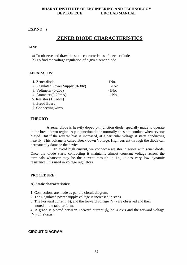
To avoid high current, we connect a resistor in series with zener diode. Once the diode starts conducting it maintains almost constant voltage across the terminals whatever may be the current through it, i.e., it has very low dynamic resistance. It is used in voltage regulators. PROCEDURE: A) Static characteristics: 1. Connections are made as per the circuit diagram. 2. The Regulated power supply voltage is increased in steps. 3. The Forward current (lf), and the forward voltage (Vf.) are observed and then noted in the tabular form. 4. A graph is plotted between Forward current (lf) on X-axis and the forward voltage (Vf) on Y-axis.
CIRCUIT DIAGRAM

BHARAT INSTITUTE OF ENGINEERING AND TECHNOLOGY DEPT.OF ECE EDC LAB MANUAL
33
A) STATIC CHARACTERISTICS :
B) REGULATION CHARACTERISTICS:
Model Graph:
BHARAT INSTITUTE OF ENGINEERING AND TECHNOLOGY DEPT.OF ECE EDC LAB MANUAL
34
B) Regulation characteristics: 1. Connection are made as per the circuit diagram 2. The load is placed in full load condition and the zener voltage (Vz), Zener current
(lz), load current (IL) are measured. 3. The above step is repeated by decreasing the value of the load in steps. 4. All the readings are tabulated. 5. The percentage regulation is calculated using the below formula 6. The voltage regulation of any device is usually expressed as percentage regulation. The percentage regulation is given by the formula ((VNL-VFL)/VFL)X100 VNL=Voltage across the diode, when no load is connected. VFL=Voltage across the diode, when load is connected.
PRECAUTIONS:
1. The terminals of the zener diode should be properly identified 2. While determined the load regulation, load should not be immediately shorted. 3. Should be ensured that the applied voltages & currents do not exceed the ratings of
the diode.
VIVAQUESTIONS: 1. What type of temp? Coefficient does the zener diode have? 2. If the impurity concentration is increased, how the depletion width effected? 3. Does the dynamic impendence of a zener diode vary? 4. Explain briefly about avalanche and zener breakdowns? 5. Draw the zener equivalent circuit? 6. Differentiate between line regulation & load regulation? 7. In which region zener diode can be used as a regulator? 8. How the breakdown voltage of a particular diode can be controlled? 9. What type of temperature coefficient does the Avalanche breakdown has? 10. By what type of charge carriers the current flows in zener and avalanche breakdown
diodes?

BHARAT INSTITUTE OF ENGINEERING AND TECHNOLOGY DEPT.OF ECE EDC LAB MANUAL
35
OBSERVATIONS: A) Static characteristics :
S.NO Applied Voltage(V) Forward Voltage(Vf) Forward Current(I f(mA))
B)Regulation Characteristics:
S.No
Applied Voltage,V
s
VNL (VOLTS
)
VFL (VOLTS
)
RL (KΏ
)
% REGULATIO
N
RESULT: Thus, we have drawn the static characteristics of zener diode and
also observed that its regulation Charactristics.

BHARAT INSTITUTE OF ENGINEERING AND TECHNOLOGY DEPT.OF ECE EDC LAB MANUAL
36
EXP.NO: 3
Input and output characteristic of Transistor in CB
configuration
AIM: 1.To observe and draw the input and output characteristics of a transistor connected in common base configuration.
2. To find α of the given transistor and also its input and output Resistances.
APPARATUS: Transistor, BC107 -1No.
Regulated power supply (0-30V) -1No. Voltmeter (0-20V) - 2No. Ammeters (0-10mA) -2No. Resistor, 1KΩ -2No Bread board Connecting wires THEORY:
A transistor is a three terminal active device. The terminals are emitter, base, collector. In CB configuration, the base is common to both input (emitter) and output (collector). For normal operation, the E-B junction is forward biased and C-B junction is reverse biased. In CB configuration, IE is +ve, IC is –ve and IB is –ve. So,
VEB = F1 (VCB, IE) and
IC = F2 (VEB,IB)
With an increasing the reverse collector voltage, the space-charge width at the output junction increases and the effective base width ‘W’ decreases. This phenomenon is known as “Early effect”. Then, there will be less chance for recombination within the base region. With increase of charge gradient with in the base region, the current of minority carriers injected across the emitter junction increases. The current amplification factor of CB configuration is given by,
α = ∆IC/ ∆IE
Input Resistance, ri = ∆VBE /∆IE at Constant VCB
Output Résistance, ro = ∆VCB /∆IC at Constant IE

BHARAT INSTITUTE OF ENGINEERING AND TECHNOLOGY DEPT.OF ECE EDC LAB MANUAL
37
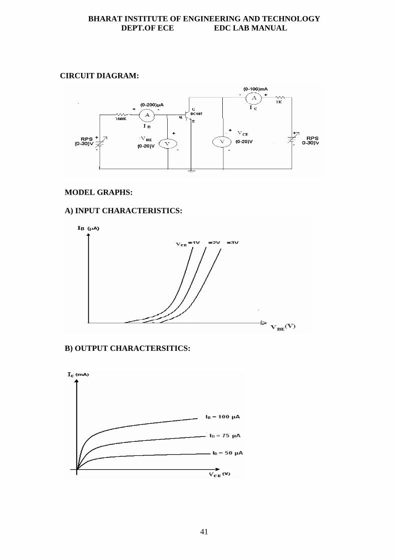
CIRCUIT DIAGRAM:
MODEL GRAPHS:
A) INPUT CHARACTERISTICS
B) OUTPUTCHARACTERISTICS

BHARAT INSTITUTE OF ENGINEERING AND TECHNOLOGY DEPT.OF ECE EDC LAB MANUAL
38
PROCEDURE:
A) INPUT CHARACTERISTICS:
1. Connections are made as per the circuit diagram. 2. For plotting the input characteristics, the output voltage VCE is kept constant at 0V and for different values of VEE ,note down the values of IE and VBE 3. Repeat the above step keeping VCB at 2V, 4V, and 6V and all the readings are tabulated. 4. A graph is drawn between VEB and IE for constant VCB.
B) OUTPUT CHARACTERISTICS:
1. Connections are made as per the circuit diagram. 2. For plotting the output characteristics, the input IE is kept constant at 0.5mA and for
different values of VCC, note down the values of IC and VCB. 3. Repeat the above step for the values of IE at 1mA, 5mA and all the readings are
tabulated. 4. A graph is drawn between VCB and Ic for constant IE
PRECAUTIONS:
1. The supply voltages should not exceed the rating of the transistor. 2. Meters should be connected properly according to their polarities.
VIVA QUESTIONS:
1. What is the range of α for the transistor? 2. Draw the input and output characteristics of the transistor in CB configuration? 3. Identify various regions in output characteristics? 4. What is the relation between α and β? 5. What are the applications of CB configuration? 6. What are the input and output impedances of CB configuration? 7. Define α (alpha)? 8. What is early effect? 9. Draw Circuit diagram of CB configuration for PNP transistor? 10. What is the power gain of CB configuration?
BHARAT INSTITUTE OF ENGINEERING AND TECHNOLOGY DEPT.OF ECE EDC LAB MANUAL
39
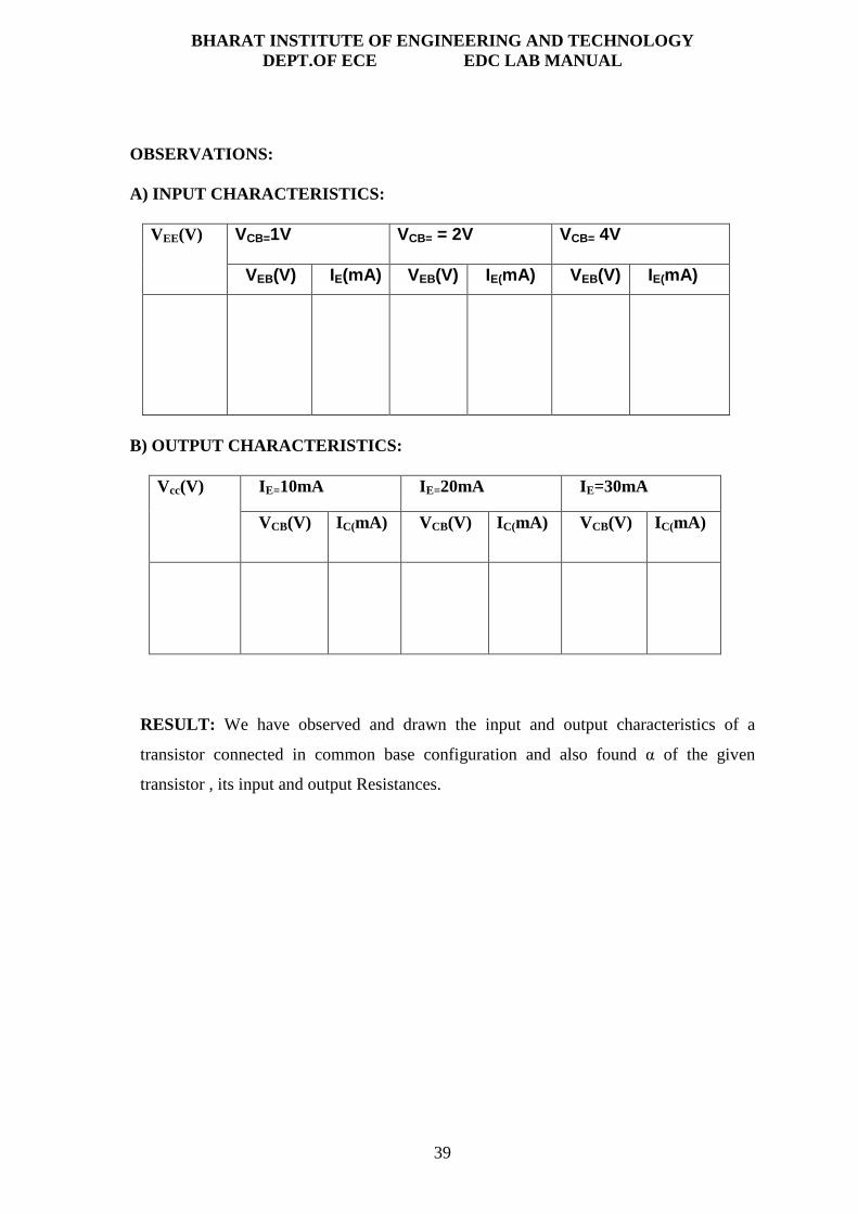
OBSERVATIONS: A) INPUT CHARACTERISTICS:
VCB=1V VCB= = 2V VCB= 4V
VEE(V)
VEB(V) IE(mA) VEB(V) IE(mA) VEB(V) IE(mA)
B) OUTPUT CHARACTERISTICS:
IE=10mA IE=20mA IE=30mA Vcc(V)
VCB(V) I C(mA) VCB(V) I C(mA) VCB(V) I C(mA)
RESULT: We have observed and drawn the input and output characteristics of a
transistor connected in common base configuration and also found α of the given
transistor , its input and output Resistances.

BHARAT INSTITUTE OF ENGINEERING AND TECHNOLOGY DEPT.OF ECE EDC LAB MANUAL
40
EXP.NO: 4
Input and output characteristic of Transistor in CE configuration
AIM:
1. To draw the input and output characteristics of transistor connected in CE configuration 2. To find β of the given transistor and also its input and output Resistances
APPARATUS: Transistor, BC107 -1No.
Regulated power supply (0-30V) -1No. Voltmeter (0-20V) - 2No. Ammeters (0-20mA) -1No. Ammeters (0-200µA) -1No. Resistor, 100Ω -1No Resistor, 1KΩ -1No. Bread board Connecting wires THEORY: In common emitter configuration, input voltage is applied between base and emitter terminals and out put is taken across the collector and emitter terminals. Therefore the emitter terminal is common to both input and output. The input characteristics resemble that of a forward biased diode curve. This is expected since the Base-Emitter junction of the transistor is forward biased. As compared to CB arrangement IB increases less rapidly with VBE. Therefore input resistance of CE circuit is higher than that of CB circuit. The output characteristics are drawn between Ic and VCE at constant IB. the collector current varies with VCE upto few volts only. After this the collector current becomes almost constant, and independent of VCE. The value of VCE up to which the collector current changes with V CE is known as Knee voltage. The transistor always operated in the region above Knee voltage, IC is always constant and is approximately equal to IB.The current amplification factor of CE configuration is given by β = ∆IC/∆IB
Input Resistance, ri = ∆VBE /∆IB (µA) at Constant VCE
Output Résistance, ro = ∆VCE /∆IC at Constant IB (µA)
BHARAT INSTITUTE OF ENGINEERING AND TECHNOLOGY DEPT.OF ECE EDC LAB MANUAL
41
CIRCUIT DIAGRAM:
MODEL GRAPHS: A) INPUT CHARACTERISTICS:
B) OUTPUT CHARACTERSITICS:

BHARAT INSTITUTE OF ENGINEERING AND TECHNOLOGY DEPT.OF ECE EDC LAB MANUAL
42
PROCEDURE:
A) INPUT CHARECTERSTICS:
1. Connect the circuit as per the circuit diagram. 2. For plotting the input characteristics the output voltage VCE is kept constant at 1V
and for different values of VBB , note down the values of IB and VBE 3. Repeat the above step by keeping VCE at 2V and 4V and tabulate all the readings. 4. plot the graph between VBE and IB for constant VCE
B) OUTPUT CHARACTERSTICS:
1. Connect the circuit as per the circuit diagram 2. for plotting the output characteristics the input current IB is kept constant at
50µA and for different values of VCC note down the values of IC and VCE 3. Repeat the above step by keeping IB at 75 µA and 100 µA and tabulate the all the
readings 4. plot the graph between VCE and IC for constant IB
PRECAUTIONS:
1. The supply voltage should not exceed the rating of the transistor 2. Meters should be connected properly according to their polarities VIVA QUESTIONS:
1. What is the range of β for the transistor? 2. What are the input and output impedances of CE configuration? 3. Identify various regions in the output characteristics? 4. What is the relation between α and β? 5. Define current gain in CE configuration? 6. Why CE configuration is preferred for amplification? 7. What is the phase relation between input and output? 8. Draw diagram of CE configuration for PNP transistor? 9. What is the power gain of CE configuration? 10. What are the applications of CE configuration?

BHARAT INSTITUTE OF ENGINEERING AND TECHNOLOGY DEPT.OF ECE EDC LAB MANUAL
43
OBSERVATIONS:
A) INPUT CHARACTERISTICS:
VCE = 1V VCE = 2V VCE = 4V
VBB
VBE(V) IB(µA) VBE(V) IB(µA) VBE(V) IB(µA)
B) OUTPUT CHAREACTARISTICS:
IB = 50 µA I B = 75 µA I B = 100 µA .NO
VCE(V) IC(mA) VCE(V) I C(mA) VCE(V) IC(mA)
RESULT: Thus, We have drawn the input and output characteristics of transistor connected in CE configuration and we found β of the given transistor and also its input and output Resistances

BHARAT INSTITUTE OF ENGINEERING AND TECHNOLOGY DEPT.OF ECE EDC LAB MANUAL
44
EXP.NO: 5
5.HALF WAVE RECTIFIER WITH AND WITHOUT FILTERS
AIM: To examine the input and output waveforms of half wave Rectifier and also
calculate its load regulation and ripple factor. 1. with Filter 2. without Filter
APPARATUS:
Digital multimetersMultimeter - 1No. Transformer (6V-0-6V) - 1No. Diode, 1N4007 - 1No. Capacitor 100µf/470 µf - 1No. Decade Resistance Box - 1No. Breadboard CRO and CRO probes Connecting wires
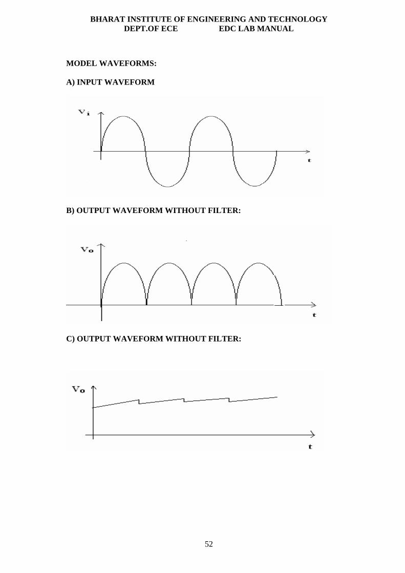
THEORY: In Half Wave Rectification, When AC supply is applied at the input, only Positive Half Cycle appears across the load whereas, the negative Half Cycle is suppressed. How this can be explained as follows: During positive half-cycle of the input voltage, the diode D1 is in forward bias and conducts through the load resistor RL. Hence the current produces an output voltage across the load resistor RL, which has the same shape as the +ve half cycle of the input voltage.
During the negative half-cycle of the input voltage, the diode is reverse biased
and there is no current through the circuit. i.e., the voltage across RL is zero. The net result is that only the +ve half cycle of the input voltage appears across the load. The average value of the half wave rectified o/p voltage is the value measured on dc voltmeter. For practical circuits, transformer coupling is usually provided for two reasons.
1. The voltage can be stepped-up or stepped-down, as needed. 2. The ac source is electrically isolated from the rectifier. Thus preventing shock
hazards in the secondary circuit. The efficiency of the Half Wave Rectifier is 40.6%

BHARAT INSTITUTE OF ENGINEERING AND TECHNOLOGY DEPT.OF ECE EDC LAB MANUAL
45
CIRCUIT DIAGRAM: A) Half wave Rectifier without filter:
B) Half wave Rectifier with filter

BHARAT INSTITUTE OF ENGINEERING AND TECHNOLOGY DEPT.OF ECE EDC LAB MANUAL
46
PROCEDURE: 1. Connections are made as per the circuit diagram. 2. Connect the primary side of the transformer to ac mains and the secondary side to the rectifier input. 3. By the multimeter, measure the ac input voltage of the rectifier and, ac and dc voltage at the output of the rectifier.
4. Find the theoretical of dc voltage by using the formula, Vdc=Vm/П
Where, Vm=2Vrms, (Vrms=output ac voltage.) 5. The Ripple factor is calculated by using the formula
r = ac output voltage/dc output voltage.
REGULATION CHARACTERSTICS:
1. Connections are made as per the circuit diagram. 2. By increasing the value of the rheostat, the voltage across the load and current
flowing through the load are measured. 3. The reading is tabulated. 4. From the value of no-load voltages, the %regulation is calculated using the
formula, %Regulation = [(VNL-VFL) /VFL]*100
Theoretical calculations for Ripple factor:
Without Filter :
Vrms=Vm/2
Vm=2Vrms
Vdc=Vm/П
Ripple factor r=√ (Vrms/ Vdc )2 -1 =1.21
With Filter:
Ripple factor, r=1/ (2√3 f C R)

BHARAT INSTITUTE OF ENGINEERING AND TECHNOLOGY DEPT.OF ECE EDC LAB MANUAL
47
MODEL WAVEFORMS: A) INPUT WAVEFORM
B) OUTPUT WAVFORM WITHOUT FILTER
C) OUTPUT WAVEFORM WITH FILTER:

BHARAT INSTITUTE OF ENGINEERING AND TECHNOLOGY DEPT.OF ECE EDC LAB MANUAL
48
PRECAUTIONS:
1. The primary and secondary side of the transformer should be carefully identified 2. The polarities of all the diodes should be carefully identified. 3. While determining the % regulation, first Full load should be applied and then it should be decremented in steps.
VIVA QUESTIONS:
1. What is the PIV of Half wave rectifier? 2. What is the efficiency of half wave rectifier? 3. What is the rectifier? 4. What is the difference between the half wave rectifier and full wave Rectifier? 5. What is the o/p frequency of Bridge Rectifier? 6. What are the ripples? 7. What is the function of the filters? 8. What is TUF? 9. What is the average value of o/p voltage for HWR? 10. What is the peak factor?
RESULT: We have examined the input and output waveforms of half wave Rectifier and also calculate its load regulation and ripple factor. 1. with Filter 2. without Filter

BHARAT INSTITUTE OF ENGINEERING AND TECHNOLOGY DEPT.OF ECE EDC LAB MANUAL
49
EXP.NO: 6
FULL WAVE RECTIFIER WITH AND WITHOUT
FILTERS
AIM: To Examine the input and output waveforms of Full Wave Rectifier and also calculate its load regulation and ripple factor. 1. with Filter 2. without Filter
APPARATUS:
Digital multimetersMultimeter - 1No.
Transformer (6V-0-6V) - 1No. Diode, 1N4007 - 2No. Capacitor 100µf/470 µf - 1No. Decade Resistance Box - 1 No. Breadboard CRO and CRO probes Connecting wires
THEORY:
The circuit of a center-tapped full wave rectifier uses two diodes D1&D2. During positive half cycle of secondary voltage (input voltage), the diode D1 is forward biased and D2is reverse biased. So the diode D1 conducts and current flows through load resistor RL.
During negative half cycle, diode D2 becomes forward biased and D1 reverse
biased. Now, D2 conducts and current flows through the load resistor RL in the same direction. There is a continuous current flow through the load resistor RL, during both the half cycles and will get unidirectional current as show in the model graph. The difference between full wave and half wave rectification is that a full wave rectifier allows unidirectional (one way) current to the load during the entire 360 degrees of the input signal and half-wave rectifier allows this only during one half cycle (180 degree).

BHARAT INSTITUTE OF ENGINEERING AND TECHNOLOGY DEPT.OF ECE EDC LAB MANUAL
50
CIRCUIT DIAGRAM: A) FULL WAVE RECTIFIER WITHOUT FILTER:
B) FULL WAVE RECTIFIER WITH FILTER:

BHARAT INSTITUTE OF ENGINEERING AND TECHNOLOGY DEPT.OF ECE EDC LAB MANUAL
51
PROCEDURE:
1. Connections are made as per the circuit diagram. 2. Connect the ac mains to the primary side of the transformer and the secondary
side to the rectifier. 3. Measure the ac voltage at the input side of the rectifier. 4. Measure both ac and dc voltages at the output side the rectifier. 5. Find the theoretical value of the dc voltage by using the formula Vdc=2Vm/П 6. Connect the filter capacitor across the load resistor and measure the values of
Vac and Vdc at the output. 7. The theoretical values of Ripple factors with and without capacitor are
calculated. 8. From the values of Vac and Vdc practical values of Ripple factors are
calculated. The practical values are compared with theoretical values. THEORITICAL CALCULATIONS: Vrms = Vm/ √2 Vm =Vrms√2 Vdc=2Vm/П (i)Without filter : Ripple factor, r = √ (Vrms/ Vdc )2 -1 = 0.812 (ii)With filter : Ripple factor, r = 1/ (4√3 f C RL)
BHARAT INSTITUTE OF ENGINEERING AND TECHNOLOGY DEPT.OF ECE EDC LAB MANUAL
52
MODEL WAVEFORMS: A) INPUT WAVEFORM
B) OUTPUT WAVEFORM WITHOUT FILTER:
C) OUTPUT WAVEFORM WITHOUT FILTER:

BHARAT INSTITUTE OF ENGINEERING AND TECHNOLOGY DEPT.OF ECE EDC LAB MANUAL
53
PRECAUTIONS:
1. The primary and secondary side of the transformer should be carefully identified. 2. The polarities of all the diodes should be carefully identified.
VIVA QUESTIONS :
1. Define regulation of the full wave rectifier? 2. Define peak inverse voltage (PIV)? And write its value for Full-wave rectifier? 3. If one of the diode is changed in its polarities what wave form would you get? 4. Does the process of rectification alter the frequency of the waveform? 5. What is ripple factor of the Full-wave rectifier? 6. What is the necessity of the transformer in the rectifier circuit? 7. What are the applications of a rectifier? 8. What is meant by ripple and define Ripple factor? 9. Explain how capacitor helps to improve the ripple factor? 10. Can a rectifier made in INDIA (V=230v, f=50Hz) be used in USA (V=110v,
f=60Hz)?
RESULT: We have examined the input and output waveforms of Full Wave Rectifier and also calculate its load regulation and ripple factor. 1. with Filter 2. without Filter

BHARAT INSTITUTE OF ENGINEERING AND TECHNOLOGY DEPT.OF ECE EDC LAB MANUAL
54
Exp.NO.7 FET CHARACTERISTICS
AIM: a). To draw the drain and transfer characteristics of a given FET.
b). To find the drain resistance (rd) amplification factor (µ) and TransConductance (gm) of the given FET.
APPARATUS: FET BFW11 -1No.
Regulated power supply (0-30V) -1No. Voltmeter (0-20V) -2No. Ammeter (0-20mA) -1No. Bread board Connecting wires
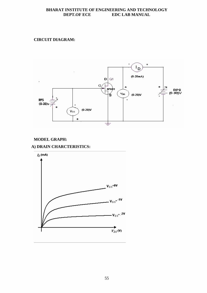
THEORY: A FET is a three terminal device, in which current conduction is by majority carriers only. The flow of current is controlled by means of an Electric field. The three terminals of FET are Gate, Drain and Source. It is having the characteristics of high input impedance and less noise, the Gate to Source junction of the FETs always reverse biased. In response to small applied voltage from drain to source, the n-type bar acts as sample resistor, and the drain current increases linearly with VDS. With increase in ID the ohmic voltage drop between the source and the channel region reverse biases the junction and the conducting position of the channel begins to remain constant. The VDS at this instant is called “pinch of voltage”. If the gate to source voltage (VGS) is applied in the direction to provide additional reverse bias, the pinch off voltage ill is decreased. In amplifier application, the FET is always used in the region beyond the pinch-off. FET parameters:
AC Drain Resistance, rd = ∆VDS / ∆I D at constant VGS
Tran conductance, gm = ∆ID /∆VGS at constant VDS
Amplification, µ = ∆VDS/∆VGS at constant ID
Relation between above parameters µ = rd * gm The drain current is given by .
ID =IDSS (1-VGS/VP) 2
BHARAT INSTITUTE OF ENGINEERING AND TECHNOLOGY DEPT.OF ECE EDC LAB MANUAL
55
CIRCUIT DIAGRAM:
MODEL GRAPH:
A) DRAIN CHARCTERISTICS:

BHARAT INSTITUTE OF ENGINEERING AND TECHNOLOGY DEPT.OF ECE EDC LAB MANUAL
56
B) TRANSFER CHARACTERISTICS:
OBSERVATIONS:
A) DRAIN CHARACTERISTICS:
S.NO VGS = 0V VGS = 0.1V VGS = 0.2V
VDS(V) I D(mA) VDS(V) I D(mA) VDS(V) I D(mA)
B) TRANSFER CHARACTERISTICS:
S.NO VDS =0.5V VDS = 1V VDS = 1.5V
VGS (V) ID(mA) VGS (V) ID(mA) VGS (V) ID(mA)
BHARAT INSTITUTE OF ENGINEERING AND TECHNOLOGY DEPT.OF ECE EDC LAB MANUAL
57
PROCEDURE:
2. All the connections are made as per the circuit diagram. 3. To plot the drain characteristics, keep VGS constant at 0V. 4. Vary the VDD and observe the values of VDS and ID. 5. Repeat the above steps 2, 3 for different values of VGS at 0.1V and 0.2V. 6. All the readings are tabulated. 7. To plot the transfer characteristics, keep VDS constant at 1V. 8. Vary VGG and observe the values of VGS and ID. 9. Repeat steps 6 and 7 for different values of VDS at 1.5 V and 2V. 10. The readings are tabulated. 11. From drain characteristics, calculate the values of dynamic resistance (rd) 12. From transfer characteristics, calculate the value of transconductace (gm) 13. And also calculate Amplification factor (µ).
PRECAUTIONS:
1. The three terminals of the FET must be care fully identified 2. Practically FET contains four terminals, which are called source, drain, Gate,
substrate. 3. Source and case should be short circuited. 4. Voltages exceeding the ratings of the FET should not be applied.
RESULT: We have Drawn the drain and transfer characteristics of a given FET.And
We have found the drain resistance (rd) amplification factor (µ) and Trans Conductance
(gm) of the given FET.
VIVA QUESTIONS:
1. What are the advantages of FET? 2. Different between FET and BJT? 3. Explain different regions of V-I characteristics of FET? 4. What are the applications of FET? 5. What are the types of FET? 6. Draw the symbol of FET. 7. What are the disadvantages of FET? 8. What are the parameters of FET?
BHARAT INSTITUTE OF ENGINEERING AND TECHNOLOGY DEPT.OF ECE EDC LAB MANUAL
58
Exp. No:8
MEASUREMENT OF h-PARAMETERS OF TRASISTOR IN CE CONFIGURATION
AIM: To calculate the h-parameters of transistor in CE configuration.
APPRATUS:
Transistor BC107 -1No.
Resistors 100 K Ώ 100 Ώ -1No.Each
Ammeter (0-200µA) -1No.
Ammeter(0-200mA) -1No.
Voltmeter (0-20V) -2Nos Regulated Power Supply (0-30V) - 2Nos Breadboard
THEORY:
A) INPUT CHARACTERISTICS:
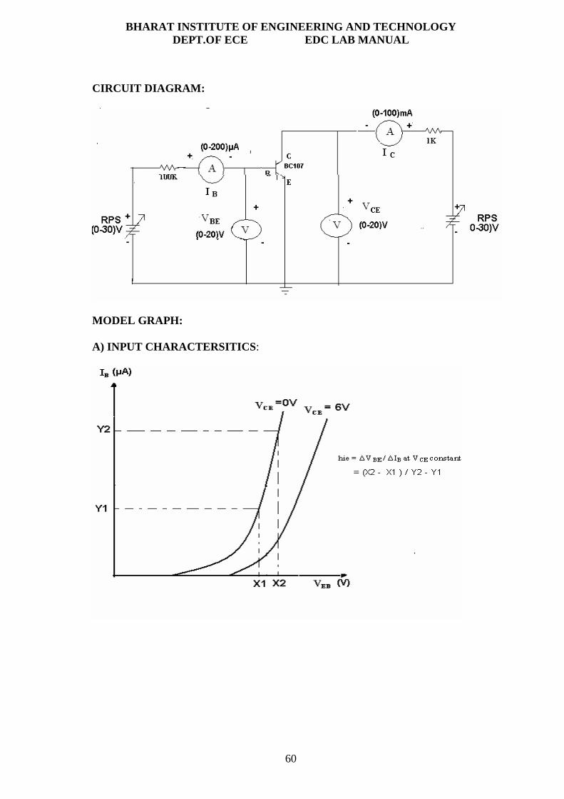
The two sets of characteristics are necessary to describe the behaviour of the CE configuration, in which one for input or base emitter circuit and other for the output or collector emitter circuit. In input characteristics the emitter base junction forward biased by a very small voltage VBB where as collector base junction reverse biased by a very large voltage VCC. The input characteristics are a plot of input current IB Versuss the input voltage VBE for a range of values of output voltage VCE . The following important points can be observed from these characteristics curves.
1. Input resistance is high as IB increases less rapidly with VBE 2. The input resistance of the transistor is the ratio of change in base emitter voltage ∆VBE to change in base current ∆IB at constant collector emitter voltage (VCE) i.e... Input resistance or input impedance hie = ∆VBE / ∆IB at VCE constant.
B) OUTPUT CHARACTERISTICS:
A set of output characteristics or collector characteristics are a plot of out put current IC VS output voltage VCE for a range of values of input current IB .The following important points can be observed from these characteristics curves.
1. The transistor always operates in the active region. i.e. the collector current IC increases with VCE very slowly. For low values of the VCE the IC increases rapidly with a small increase in VCE .The transistor is said to be working in saturation region.

BHARAT INSTITUTE OF ENGINEERING AND TECHNOLOGY DEPT.OF ECE EDC LAB MANUAL
59
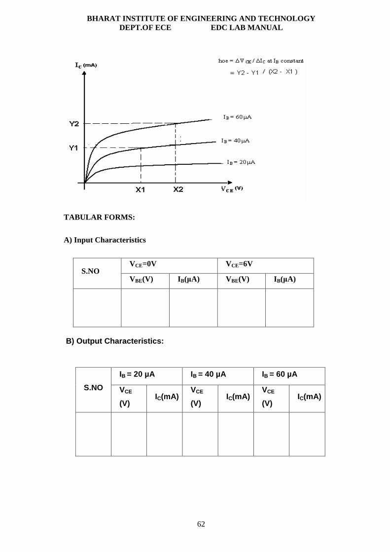
Output resistance is the ratio of change of collector emitter voltage ∆VCE , to change in collector current ∆IC with constant IB. Output resistance or Output impedance hoe = ∆VCE / ∆IC at IB constant.
Input Impedance hie = ∆VBE / ∆IB at VCE constant
Output impedance hoe = ∆VCE / ∆IC at IB constant
Reverse Transfer Voltage Gain hre = ∆VBE / ∆VCE at IB constant
Forward Transfer Current Gain hfe = ∆IC / ∆IB at constant VCE
PROCEDURE:
1. Connect a transistor in CE configuration circuit for plotting its input and output
characteristics.
2. Take a set of readings for the variations in IB with VBE at different fixed values of
output voltage VCE .
3. Plot the input characteristics of CE configuration from the above readings.
4. From the graph calculate the input resistance hie and reverse transfer ratio hre by
taking the slopes of the curves.
5. Take the family of readings for the variations of IC with VCE at different values of
fixed IB.
6. Plot the output characteristics from the above readings.
7. From the graphs, calculate hie hoe, hfe and hre by taking the slope of the curves.
BHARAT INSTITUTE OF ENGINEERING AND TECHNOLOGY DEPT.OF ECE EDC LAB MANUAL
60
CIRCUIT DIAGRAM:
MODEL GRAPH:
A) INPUT CHARACTERSITICS :

BHARAT INSTITUTE OF ENGINEERING AND TECHNOLOGY DEPT.OF ECE EDC LAB MANUAL
61
OUPUT CHARACTERISITCS:
BHARAT INSTITUTE OF ENGINEERING AND TECHNOLOGY DEPT.OF ECE EDC LAB MANUAL
62
TABULAR FORMS:
A) Input Characteristics
VCE=0V VCE=6V S.NO
VBE(V) IB(µA) VBE(V) I B(µA)
B) Output Characteristics:
IB = 20 µA IB = 40 µA IB = 60 µA
S.NO VCE
(V) IC(mA)
VCE
(V) IC(mA)
VCE
(V) IC(mA)
BHARAT INSTITUTE OF ENGINEERING AND TECHNOLOGY DEPT.OF ECE EDC LAB MANUAL
63
OBSERVATION:
1. Input Impedance hie =
2. Reverse Transfer Voltage Gain hre =
3. Forward Transfer Current Gain hfe =
4. Output conductance hoe =
RESULT: Hence, we have calculated the h-parameters of transistor in CE configuration
VIVA QUESTIONS:
1. What are the h-parameters?
2. What are the limitations of h-parameters?
3. What are its applications?
4. Draw the Equivalent circuit diagram of H parameters?
5. Define H parameter?
6. What are tabular forms of H parameters monoculture of a transistor?
7. What is the general formula for input impedance?
8. What is the general formula for Current Gain?
9. What is the general formula for Voltage gain?
BHARAT INSTITUTE OF ENGINEERING AND TECHNOLOGY DEPT.OF ECE EDC LAB MANUAL
64
Exp.No:9
FREQUENCY RESPONSE OF CE AMPLIFIER
AIM: 1. To Measure the voltage gain of a CE amplifier
2. To draw the frequency response curve of the CE amplifier
APPARATUS: Transistor BC107 -1No. Regulated power Supply (0-30V) -1No. Function Generator -1No. CRO -1No. Resistors [33KΩ, 3.3KΩ, 330Ω, -1No.Each 1.5KΩ, 1KΩ, 2.2KΩ, 4.7KΩ] Capacitors, 10µF -2No 100µF -1No. Bread Board Connecting Wires THEORY : The CE amplifier provides high gain &wide frequency response. The emitter lead is common to both input & output circuits and is grounded. The emitter-base circuit is forward biased. The collector current is controlled by the base current rather than emitter current. When a transistor is biased in active region it acts like an amplifier. The input signal is applied to base terminal of the transistor and amplifier output is taken across collector terminal. A very small change in base current produces a much larger change in collector current. When positive half-cycle is fed to the input circuit, it opposes the forward bias of the circuit which causes the collector current to decrease; it decreases the voltage more negative. Thus when input cycle varies through a negative half-cycle, increases the forward bias of the circuit, which causes the collector current to increases thus the output signal is common emitter amplifier is in out of phase with the input signal. An amplified output signal is obtained when this fluctuating collector current flows through a collector resistor,Rc.
The capacitor across the collector resistor Rc will act as a bypass capacitor. This
will improve high frequency response of amplifier.

BHARAT INSTITUTE OF ENGINEERING AND TECHNOLOGY DEPT.OF ECE EDC LAB MANUAL
65
PROCEDURE:
1. Connect the circuit as shown in circuit diagram 2. Apply the input of 20mV peak-to-peak and 1 KHz frequency using Function
Generator 3. Measure the Output Voltage Vo (p-p) for various load resistors. 4. Tabulate the readings in the tabular form. 5. The voltage gain can be calculated by using the expression , Av= (V0/V i) 6. For plotting the frequency response the input voltage is kept Constant at 20mV
peak-to-peak and the frequency is varied from 100Hz to 1MHz Using function generator
7. Note down the value of output voltage for each frequency. 8. All the readings are tabulated and voltage gain in dB is calculated by Using The
expression Av=20 log10 (V0/V i) 9. A graph is drawn by taking frequency on x-axis and gain in dB on y-axis On
Semi-log graph. 10.The band width of the amplifier is calculated from the graph Using the expression, Bandwidth, BW=f2-f1
Where f1 lower cut-off frequency of CE amplifier, and Where f2 upper cut-off frequency of CE amplifier 11. The bandwidth product of the amplifier is calculated using the Expression Gain Bandwidth product=3-dBmidband gain X Bandwidth

BHARAT INSTITUTE OF ENGINEERING AND TECHNOLOGY DEPT.OF ECE EDC LAB MANUAL
66
CIRCUIT DIAGRAM:
MODELWAVE FORMS:
A) INPUT WAVE FORM:
B) OUTPUT WAVE FORM

BHARAT INSTITUTE OF ENGINEERING AND TECHNOLOGY DEPT.OF ECE EDC LAB MANUAL
67
FREQUENCY RESPONSE
OBSERVATIONS:
INPUT VOLTAGE, Vi =20MV
LOAD
RESISTANCE(KΩ)
OUTPUT
VOLTAGE
(V0)
GAIN
AV=(V0/V i)
GAIN IN dB
Av=20log10
(V0/V i)
FREQUENCY RESPONSE: Vi=20mv
Frequency in KHZ OUTPUT
VOLTAGE(Vo)
GAIN IN
dB=20log10(vo/vi)

BHARAT INSTITUTE OF ENGINEERING AND TECHNOLOGY DEPT.OF ECE EDC LAB MANUAL
68
RESULT: We have measured the voltage gain of a CE amplifier and also drawn the frequency response curve of the CE amplifier VIVA QUESTIONS:
1. What is phase difference between input and output waveforms of CE amplifier?
2. What type of biasing is used in the given circuit?
3. If the given transistor is replaced by a p-n-p, can we get output or not?
4. What is effect of emitter-bypass capacitor on frequency response?
5. What is the effect of coupling capacitor?
6. What is region of the transistor so that it is operated as an amplifier?
7. How does transistor acts as an amplifier?
8. Draw the h-parameter model of CE amplifier?
9. What type of transistor configuration is used in intermediate stages of a multistage
amplifier?
10. What is early effect?
BHARAT INSTITUTE OF ENGINEERING AND TECHNOLOGY DEPT.OF ECE EDC LAB MANUAL
69
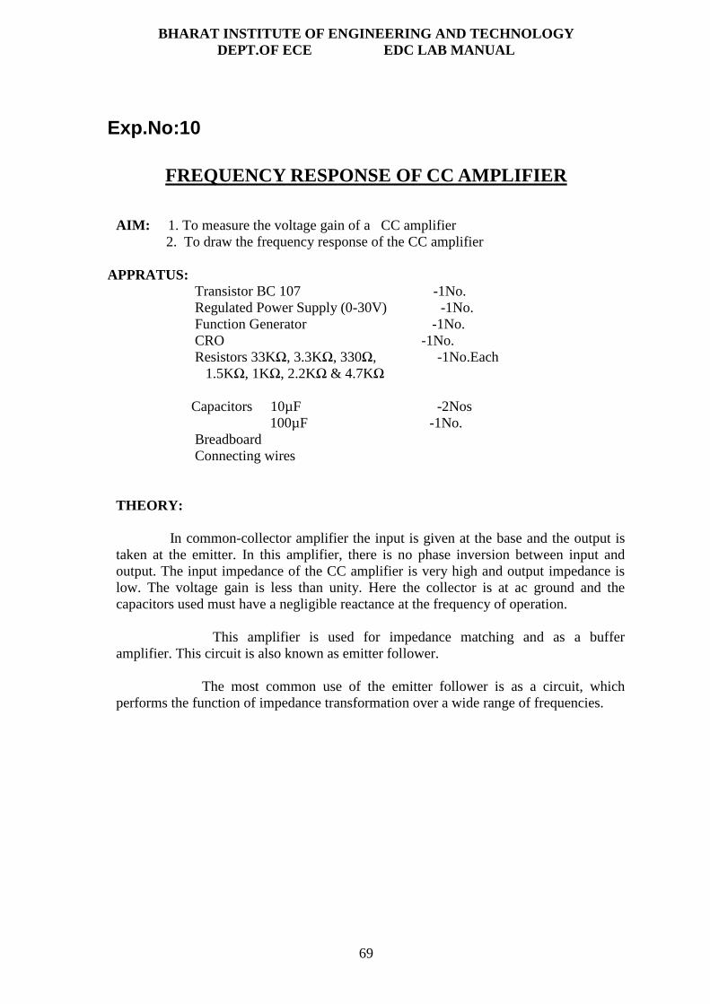
Exp.No:10
FREQUENCY RESPONSE OF CC AMPLIFIER
AIM: 1. To measure the voltage gain of a CC amplifier 2. To draw the frequency response of the CC amplifier
APPRATUS: Transistor BC 107 -1No. Regulated Power Supply (0-30V) -1No. Function Generator -1No. CRO -1No. Resistors 33KΩ, 3.3KΩ, 330Ω, -1No.Each 1.5KΩ, 1KΩ, 2.2KΩ & 4.7KΩ Capacitors 10µF -2Nos 100µF -1No. Breadboard Connecting wires THEORY: In common-collector amplifier the input is given at the base and the output is taken at the emitter. In this amplifier, there is no phase inversion between input and output. The input impedance of the CC amplifier is very high and output impedance is low. The voltage gain is less than unity. Here the collector is at ac ground and the capacitors used must have a negligible reactance at the frequency of operation. This amplifier is used for impedance matching and as a buffer amplifier. This circuit is also known as emitter follower. The most common use of the emitter follower is as a circuit, which performs the function of impedance transformation over a wide range of frequencies.
BHARAT INSTITUTE OF ENGINEERING AND TECHNOLOGY DEPT.OF ECE EDC LAB MANUAL
70
CIRCUIT DIAGRAM:
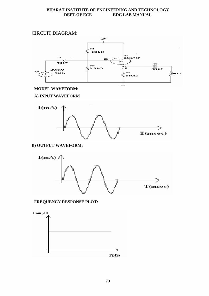
MODEL WAVEFORM:
A) INPUT WAVEFORM
B) OUTPUT WAVEFORM:
FREQUENCY RESPONSE PLOT:

BHARAT INSTITUTE OF ENGINEERING AND TECHNOLOGY DEPT.OF ECE EDC LAB MANUAL
71
OBSERVATIONS:
A) Gain ,Vi=20mV
Load
Resistance(KΩ)
output
Voltage(Vo)
Gain, Av=V0/V i Gain in dB
Av=20log
10(V0/Vi)
B) FREQUENCY RESPONSE, Vi=20mV
Frequency(HZ) Output Voltage(Vo) Gain in dB Av=20log
10(V0/Vi)
BHARAT INSTITUTE OF ENGINEERING AND TECHNOLOGY DEPT.OF ECE EDC LAB MANUAL
72
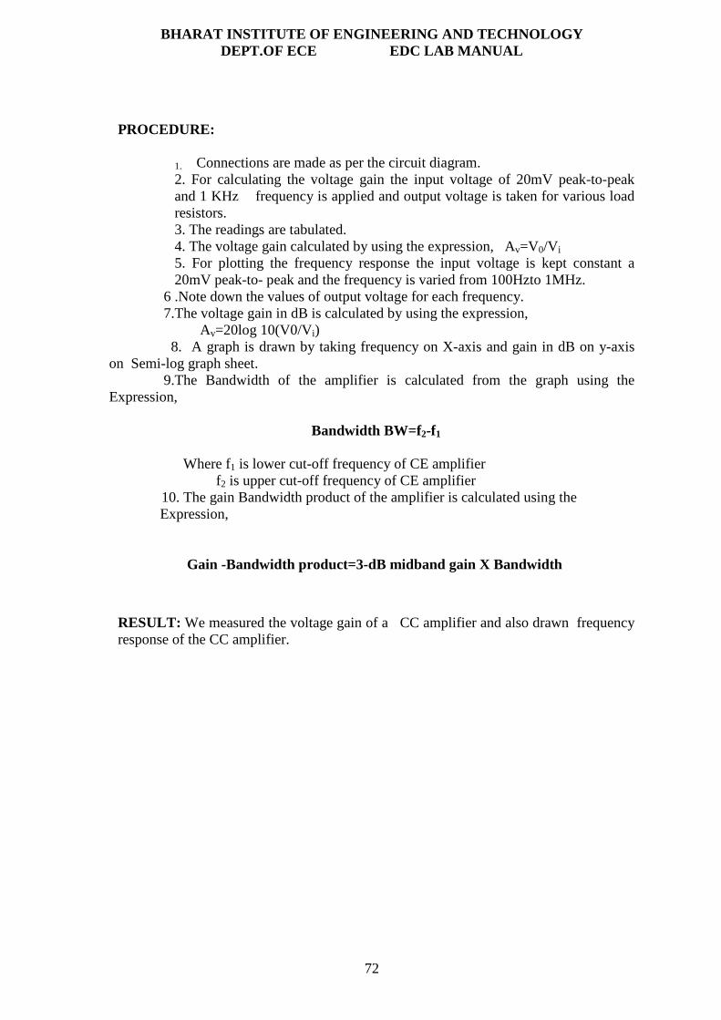
PROCEDURE:
1. Connections are made as per the circuit diagram.
2. For calculating the voltage gain the input voltage of 20mV peak-to-peak and 1 KHz frequency is applied and output voltage is taken for various load resistors. 3. The readings are tabulated. 4. The voltage gain calculated by using the expression, Av=V0/V i
5. For plotting the frequency response the input voltage is kept constant a 20mV peak-to- peak and the frequency is varied from 100Hzto 1MHz.
6 .Note down the values of output voltage for each frequency. 7.The voltage gain in dB is calculated by using the expression, Av=20log 10(V0/Vi) 8. A graph is drawn by taking frequency on X-axis and gain in dB on y-axis on Semi-log graph sheet. 9.The Bandwidth of the amplifier is calculated from the graph using the Expression,
Bandwidth BW=f 2-f1
Where f1 is lower cut-off frequency of CE amplifier f2 is upper cut-off frequency of CE amplifier 10. The gain Bandwidth product of the amplifier is calculated using the Expression, Gain -Bandwidth product=3-dB midband gain X Bandwidth
RESULT: We measured the voltage gain of a CC amplifier and also drawn frequency response of the CC amplifier.

BHARAT INSTITUTE OF ENGINEERING AND TECHNOLOGY DEPT.OF ECE EDC LAB MANUAL
73
PRECAUTIONS:
1. The input voltage must be kept constant while taking frequency response.
2. Proper biasing voltages should be applied.
VIVA QUESTIONS:
1. What are the applications of CC amplifier?
2. What is the voltage gain of CC amplifier?
3. What are the values of input and output impedances of the CC amplifier?
4. To which ground the collector terminal is connected in the circuit?
5. Identify the type of biasing used in the circuit?
6. Give the relation between α, β and γ.
7. Write the other name of CC amplifier?
8. What are the differences between CE,CB and CC?
9. When compared to CE, CC is not used for amplification. Justify your answer?
10. What is the phase relationship between input and output in CC?

BHARAT INSTITUTE OF ENGINEERING AND TECHNOLOGY DEPT.OF ECE EDC LAB MANUAL
74
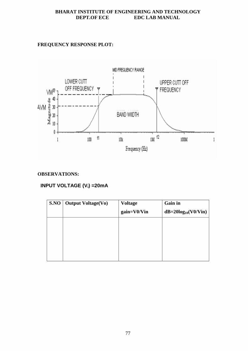
Exp.No:11 FREQUENCY RESPONSE OF COMMON SOURCE FET AMPLIFIER
AIM: 1. To obtain the frequency response of the common source FET Amplifier 2. To find the Bandwidth.
APPRATUS:
N-channel FET (BFW11) -1No. Resistors (6.8KΩ, 1MΩ, 1.5KΩ) -1No.Each Capacitors 0.1µF, -2Nos 47µF -1No. Regulated power Supply (0-30V) -1No. Function generator -1No. CRO -1No. CRO probes -1pair Bread board Connecting wires
THEORY:
A field-effect transistor (FET) is a type of transistor commonly used for weak-signal amplification (for example, for amplifying wireless (signals). The device can amplify analog or digital signals. It can also switch DC or function as an oscillator. In the FET, current flows along a semiconductor path called the channel. At one end of the channel, there is an electrode called the source. At the other end of the channel, there is an electrode called the drain. The physical diameter of the channel is fixed, but its effective electrical diameter can be varied by the application of a voltage to a control electrode called the gate. Field-effect transistors exist in two major classifications. These are known as the junction FET (JFET) and the metal-oxide- semiconductor FET (MOSFET). The junction FET has a channel consisting of N-type semiconductor (N-channel) or P-type semiconductor (P-channel) material; the gate is made of the opposite semiconductor type. In P-type material, electric charges are carried mainly in the form of electron deficiencies called holes. In N-type material, the charge carriers are primarily electrons. In a JFET, the junction is the boundary between the channel and the gate. Normally, this P-N junction is reverse-biased (a DC voltage is applied to it) so that no current flows between the channel and the gate. However, under some conditions there is a small current through the junction during part of the input signal cycle. The FET has some advantages and some disadvantages relative to the bipolar transistor. Field-effect transistors are preferred for weak-signal work, for example in wireless, communications and broadcast receivers. They are also preferred in circuits and systems requiring high impedance. The FET is not, in general, used for high-power amplification, such as is required in large wireless communications and broadcast transmitters.
BHARAT INSTITUTE OF ENGINEERING AND TECHNOLOGY DEPT.OF ECE EDC LAB MANUAL
75
Field-effect transistors are fabricated onto silicon integrated circuit (IC) chips. A single IC can contain many thousands of FETs, along with other components such as resistors, capacitors, and diodes.
A common source amplifier FET amplifier has high input impedance and a moderate voltage gain. Also, the input and output voltages are 180 degrees out of Phase.
PROCEDURE :
1. Connections are made as per the circuit diagram. 2. A signal of 1 KHz frequency and 20mV peak-to-peak is applied at the Input of amplifier. 3. Output is taken at drain and gain is calculated by using the expression,
Av=V0/V i
4. Voltage gain in dB is calculated by using the expression, Av=20log 10(V0/Vi)
5. Repeat the above steps for various input voltages. 6. Plot Av in dB Versus Frequency
7. The Bandwidth of the amplifier is calculated from the graph using the Expression,
Bandwidth BW=f 2-f1
Where f1 is lower 3 dB frequency f2 is upper 3 dB frequency
Calculations: BW= f2-f1 = RESULT : We have obtained the frequency response of the common source FET Amplifier and also found its Bandwidth.

BHARAT INSTITUTE OF ENGINEERING AND TECHNOLOGY DEPT.OF ECE EDC LAB MANUAL
76
CIRCUIT DIAGRAM :
MODEL GRAPH:
A) INPUT WAVEFORM
B) OUTPUT WAVEFORM
BHARAT INSTITUTE OF ENGINEERING AND TECHNOLOGY DEPT.OF ECE EDC LAB MANUAL
77
FREQUENCY RESPONSE PLOT:
OBSERVATIONS:
INPUT VOLTAGE (V i) =20mA
S.NO Output Voltage(Vo) Voltage
gain=V0/Vin
Gain in
dB=20log10(V0/Vin)
BHARAT INSTITUTE OF ENGINEERING AND TECHNOLOGY DEPT.OF ECE EDC LAB MANUAL
78
PRECAUTIONS:
1. All the connections should be tight.
2. Transistor terminals must be identified properly
VIVA QUESTIONS:
1. What is the difference between FET and BJT?
2. FET is unipolar or bipolar?
3. Draw the symbol of FET?
4. What are the applications of FET?
5. FET is voltage controlled or current controlled?
6. Draw the equivalent circuit of common source FET amplifier?
7. What is the voltage gain of the FET amplifier?
8. What is the input impedance of FET amplifier?
9. What is the output impedance of FET amplifier?
10. What are the FET parameters?
11. What are the FET applications
BHARAT INSTITUTE OF ENGINEERING AND TECHNOLOGY DEPT.OF ECE EDC LAB MANUAL
79
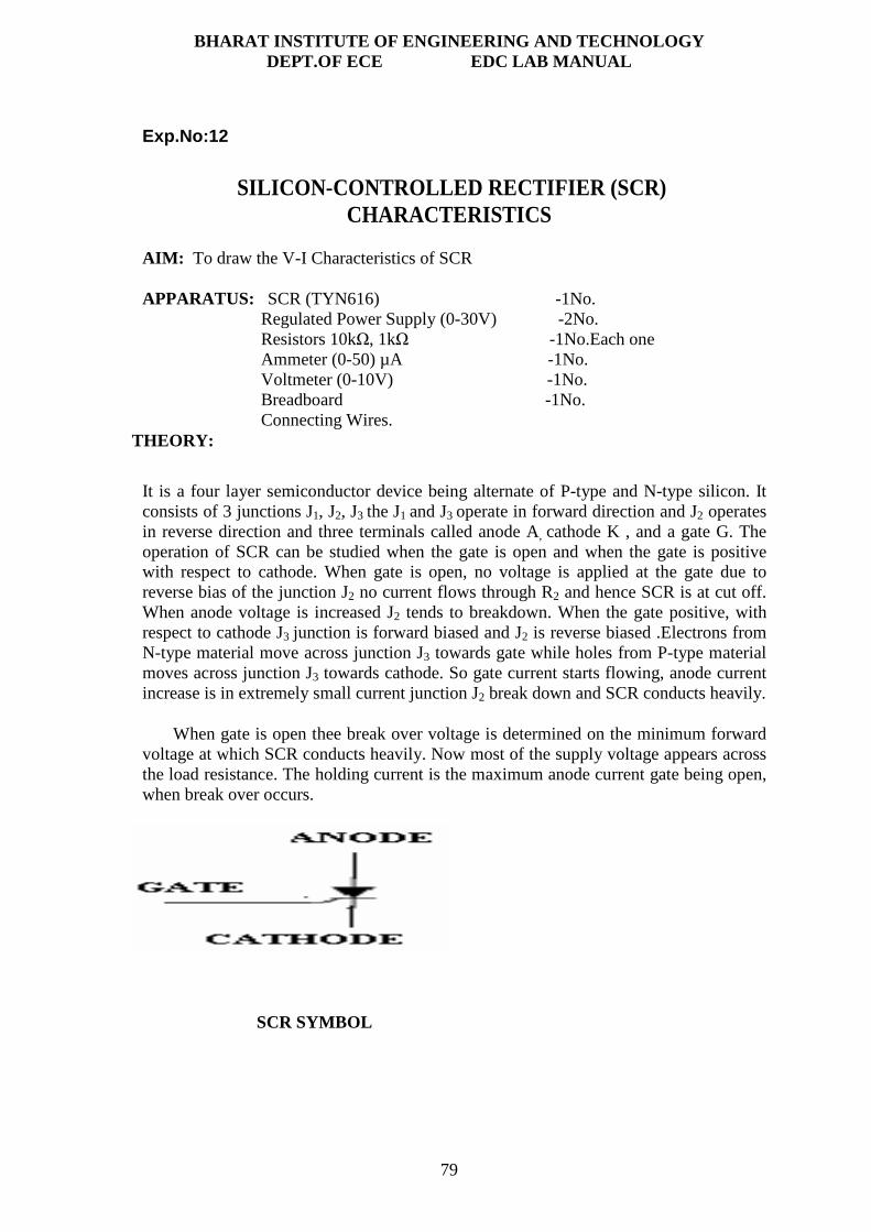
Exp.No:12
SILICON-CONTROLLED RECTIFIER (SCR) CHARACTERISTICS
AIM: To draw the V-I Characteristics of SCR
APPARATUS: SCR (TYN616) -1No. Regulated Power Supply (0-30V) -2No. Resistors 10kΩ, 1kΩ -1No.Each one Ammeter (0-50) µA -1No. Voltmeter (0-10V) -1No. Breadboard -1No. Connecting Wires.
THEORY:
It is a four layer semiconductor device being alternate of P-type and N-type silicon. It consists of 3 junctions J1, J2, J3 the J1 and J3 operate in forward direction and J2 operates in reverse direction and three terminals called anode A, cathode K , and a gate G. The operation of SCR can be studied when the gate is open and when the gate is positive with respect to cathode. When gate is open, no voltage is applied at the gate due to reverse bias of the junction J2 no current flows through R2 and hence SCR is at cut off. When anode voltage is increased J2 tends to breakdown. When the gate positive, with respect to cathode J3 junction is forward biased and J2 is reverse biased .Electrons from N-type material move across junction J3 towards gate while holes from P-type material moves across junction J3 towards cathode. So gate current starts flowing, anode current increase is in extremely small current junction J2 break down and SCR conducts heavily.
When gate is open thee break over voltage is determined on the minimum forward voltage at which SCR conducts heavily. Now most of the supply voltage appears across the load resistance. The holding current is the maximum anode current gate being open, when break over occurs.
SCR SYMBOL

BHARAT INSTITUTE OF ENGINEERING AND TECHNOLOGY DEPT.OF ECE EDC LAB MANUAL
80
CIRCUIT DIAGRAM:
MODEL WAVEFORM:
OBSERVATION:
VAK (V) I AK ( µA)

BHARAT INSTITUTE OF ENGINEERING AND TECHNOLOGY DEPT.OF ECE EDC LAB MANUAL
81
PROCEDURE:
1. Connections are made as per circuit diagram. 2. Keep the gate supply voltage at some constant value 3. Vary the anode to cathode supply voltage and note down the readings of voltmeter
and ammeter. Keep the gate voltage at standard value. 4. A graph is drawn between VAK and IAK.
RESULT: We have plotted the V-I characteristics of SCR.
VIVA QUESTIONS:
1. What the symbol of SCR? 2. In which state SCR turns of conducting state to blocking state? 3. What are the applications of SCR? 4. What is holding current? 5. What are the important type’s thyristors ? 6. How many numbers of junctions are involved in SCR? 7. What is the function of gate in SCR? 8. When gate is open, what happens when anode voltage is increased? 9. What is the value of forward resistance offered by SCR? 10. What is the condition for making from conducting state to non conducting state?

BHARAT INSTITUTE OF ENGINEERING AND TECHNOLOGY DEPT.OF ECE EDC LAB MANUAL
82
Exp.No:13
UJT CHARACTERISTICS
AIM: To observe the characteristics of UJT and to calculate the Intrinsic Stand-Off
Ratio (η).
APPARATUS: Regulated power supply (0-30V) -2Nos
0-20V (DMM) -2Nos 0-20mA (DMM) -1No. Resistors 1Kohm -2Nos Resistor 470 ohm -1No. Breadboard Connecting wires THEORY: A Unijunction Transistor (UJT) is an electronic semiconductor device that has only one junction. The UJT Unijunction Transistor (UJT) has three terminals an emitter (E) and two bases (B1 and B2). The base is formed by lightly doped n-type bar of silicon. Two ohmic contacts B1 and B2 are attached at its ends. The emitter is of p-type and it is heavily doped. The resistance between B1 and B2, when the emitter is open-circuit is called interbase resistance. The original Unijunction transistor, or UJT, is a simple device that is essentially a bar of N type semiconductor material into which P type material has been diffused somewhere along its length. The 2N2646 is the most commonly used version of the UJT.
Circuit symbol
The UJT is biased with a positive voltage between the two bases. This causes a potential drop along the length of the device. When the emitter voltage is driven approximately one diode voltage above the voltage at the point where the P diffusion (emitter) is, current will begin to flow from the emitter into the base region. Because the base region is very lightly doped, the additional current (actually charges in the base region) causes (conductivity modulation) which reduces the resistance of the portion of the base between the emitter junction and the B2 terminal. This reduction in resistance means that the emitter junction is more forward biased, and so even more current is injected. Overall, the effect is a negative resistance at the emitter terminal. This is what makes the UJT useful, especially in simple oscillator circuits. hen the emitter voltage reaches Vp, the current starts o increase and the emitter voltage starts to decrease. This is represented by negative slope of the characteristics which is referred to as the negative resistance region, beyond the valley point, RB1 reaches minimum value and this region,VEB proportional to IE.

BHARAT INSTITUTE OF ENGINEERING AND TECHNOLOGY DEPT.OF ECE EDC LAB MANUAL
83
CIRCUIT DIAGRAM:
MODEL GRAPH:
OBSEVATIONS:
VBB=10 VBB=5 VBB=2
VEB(V) IE(mA) VEB(V) I E(mA) VEB(V) I E(mA)

BHARAT INSTITUTE OF ENGINEERING AND TECHNOLOGY DEPT.OF ECE EDC LAB MANUAL
84
PROCEDURE:
1. Connection is made as per circuit diagram. 2. Output voltage is fixed at a constant level and by varying input voltage
corresponding emitter current values are noted down. 3. This procedure is repeated for different values of output voltages. 4. All the readings are tabulated and Intrinsic Stand-Off ratio is calculated using η = (Vp-VD) / VBB
5. A graph is plotted between VEE and IE for different values of VBE.
CALCULATIONS:
VP = ηVBB + VD
η = (VP-VD) / VBB
η = ( η1 + η2 + η3 ) / 3
RESULT: We have observed the characteristics of UJT and calculated the Intrinsic
Stand-Off Ratio (η).
VIVA QUESTIONS:
1. What is the symbol of UJT?
2. Draw the equivalent circuit of UJT?
3. What are the applications of UJT?
4. Formula for the intrinsic stand off ratio?
5. What does it indicates the direction of arrow in the UJT?
6. What is the difference between FET and UJT?
7. Is UJT is used an oscillator? Why?
8. What is the Resistance between B1 and B2 is called as?
9. What is its value of resistance between B1 and B2?
10. Draw the characteristics of UJT?