ecen474: (analog) vlsi circuit design fall 2010spalermo/ecen474/lecture26_ee474… · ·...
TRANSCRIPT

Sam PalermoAnalog & Mixed-Signal Center
Texas A&M University
ECEN474: (Analog) VLSI Circuit Design Fall 2010
Lecture 26: High-Speed I/O Overview

Announcements
• Project• Preliminary report due Nov 19
• This lecture is not covered in exam 3
2

3
Outline
• Introduction
• Electrical I/O Overview Channel characteristics Transmitter & receiver circuits Clocking techniques & circuits
• Future trends & optical I/O
• Conclusion

4
ECEN 689: Special Topics in High-Speed Links Circuits and Systems
• Spring 2011• http://www.ece.tamu.edu/~spalermo/ecen689.html
• Covers system level and circuit design issues relevant to high-speed electrical and optical links
• Channel Properties• Modeling, measurements, communication techniques
• Circuits• Drivers, receivers, equalizers, clocking
• Project• Link system design with statistical BER analysis tool• Circuit design of key interface circuits
• Prerequisite: ECEN 474 or my approval

5
Desktop Computer I/O Architecture
• Many high-speed I/O interfaces
• Key bandwidth bottleneck points are memory (FSB) and graphics interfaces (PCIe)
• Near-term architectures Integrated memory controller with
serial I/O (>5Gb/s) to memory Increasing PCIe from 2.5Gb/s (Gen1)
to 8Gb/s (Gen3)
• Other serial I/O systems Multi-processor systems Routers

Serial Link Applications• Processor-to-memory
• RDRAM (1.6Gbps), XDR DRAM (7.2Gbps), XDR2 DRAM (12.8Gbps)
• Processor-to-peripheral• PCIe (2.5, 5, 8Gbps), Infiniband (10Gbps), USB3 (4.8Gbps)
• Processor-to-processor• Intel QPI (6.4Gbps), AMD Hypertransport (6.4Gbps)
• Storage• SATA (6Gbps), Fibre Channel (20Gbps)
• Networks• LAN: Ethernet (1, 10Gbps)• WAN: SONET (2.5, 10, 40Gbps)• Backplane Routers: (2.5 – 12.5Gbps)
6
7
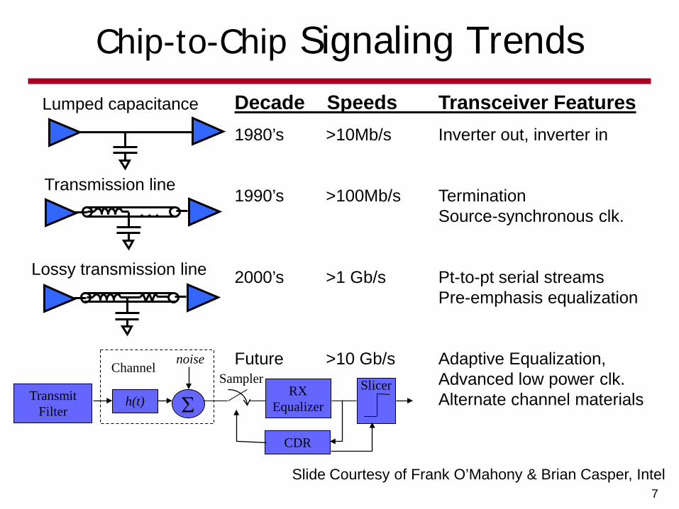
Chip-to-Chip Signaling TrendsDecade Speeds Transceiver Features1980’s >10Mb/s Inverter out, inverter in
1990’s >100Mb/s Termination Source-synchronous clk.
2000’s >1 Gb/s Pt-to-pt serial streams Pre-emphasis equalization
Future >10 Gb/s Adaptive Equalization, Advanced low power clk.Alternate channel materials
Lumped capacitance
…Transmission line
Lossy transmission line
h(t) Σ
Channel noiseSampler SlicerRX
EqualizerTransmit
Filter
CDR
Slide Courtesy of Frank O’Mahony & Brian Casper, Intel
8
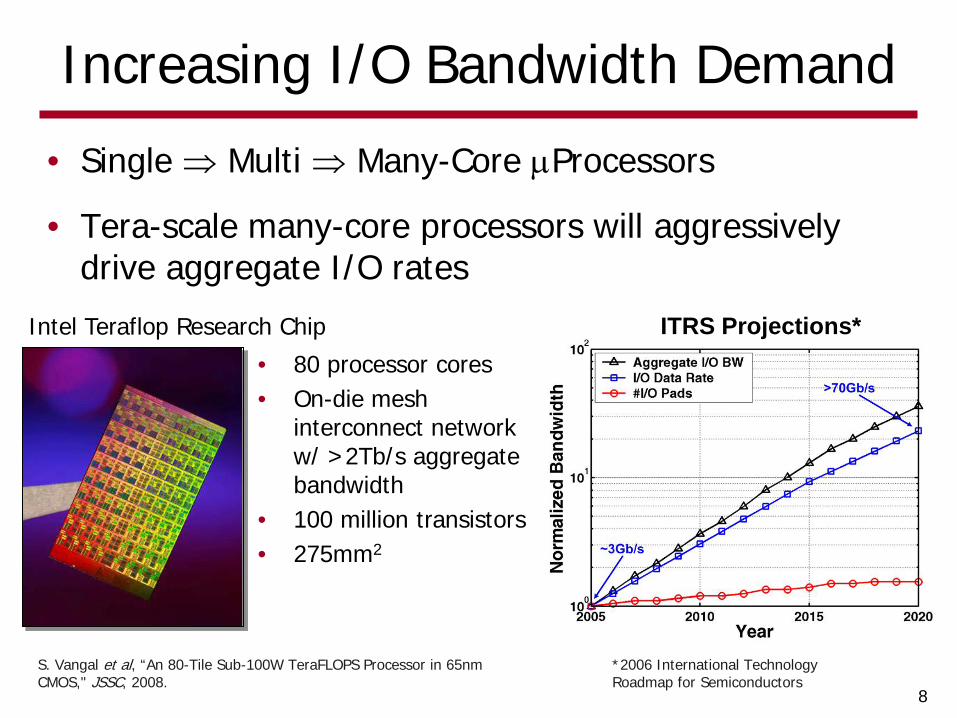
Increasing I/O Bandwidth Demand
• Single ⇒ Multi ⇒ Many-Core µProcessors
• Tera-scale many-core processors will aggressively drive aggregate I/O rates
*2006 International Technology Roadmap for Semiconductors
ITRS Projections*Intel Teraflop Research Chip
• 80 processor cores• On-die mesh
interconnect network w/ >2Tb/s aggregate bandwidth
• 100 million transistors• 275mm2
S. Vangal et al, “An 80-Tile Sub-100W TeraFLOPS Processor in 65nm CMOS," JSSC, 2008.
9
Outline
• Introduction
• Electrical I/O Overview Channel characteristics Transmitter & receiver circuits Clocking techniques & circuits
• Future trends & optical I/O
• Conclusion
10
High-Speed Electrical Link System
TX
ChannelTX
data
Seria
lizer
PLLref clk
RX
Des
eria
lizer
RXdata
TX clk RX clk
D[n+1]D[n] D[n+2] D[n+3]TX data
TX clk
RX clk
CDR

11
Electrical Backplane Channel
Line card trace(dispersion)
Backplane via(major reflections)
Backplane trace(dispersion)
Backplane connector(crosstalk)
Package via(reflections)
On-chip termination(reflections)
Chip package(crosstalk)
Line card via(reflections)
• Frequency dependent loss Dispersion & reflections
• Co-channel interference Far-end (FEXT) & near-end (NEXT) crosstalk

12
Loss Mechanisms
• Dispersion
Skin effect, αR
Dielectric loss , αD
( )( )
( )xDReV
xV αα +−=0
R0 Z0 Z0
R0
V(0) xV(x)
21
sd Depth, Skin
=
fµπρ
δ
fZDZD
LZ
R
sd
ACR
0
7
00 21061.2
22 ππδρ
α−×
===
fc
DrD
δεπα
tan=
Dispersion Loss
B. Dally et al, “Digital Systems Engineering,"

13
Reflections
0
0
ZZZZ
VV
r
r
i
r
+−
=
R0 Z0
R0
Z0
• Commonly caused by board via stubs and on-chip termination mismatches
with via stubs

14
Crosstalk
• Occurs mostly in package and board-to-board connectors
• FEXT is attenuated by channel response and has band-pass characteristic
• NEXT directly couples into victim and has high-pass characteristic
15
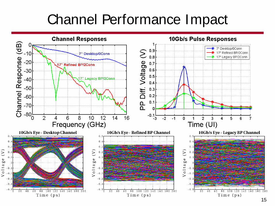
Channel Performance Impact

16
Channel Performance Impact

17
Outline
• Introduction
• Electrical I/O Overview Channel characteristics Transmitter & receiver circuits Clocking techniques & circuits
• Future trends & optical I/O
• Conclusion

18
Link Speed Limitations
• High-speed links can be limited by both the internal electronics and the channel
• Clock generation and distribution is key circuit bandwidth bottleneck Requires data mux/demux
to use multiple clock phases Passives and/or CML
techniques can extend circuit bandwidth at the expense of area and/or power
• Limited channel bandwidth is typically compensated with equalization circuits
Clock Amplitude Reduction*
*C.-K. Yang, “Design of High-Speed Serial Links in CMOS," 1998.
tFO4 in 90nm ~ 30ps
19
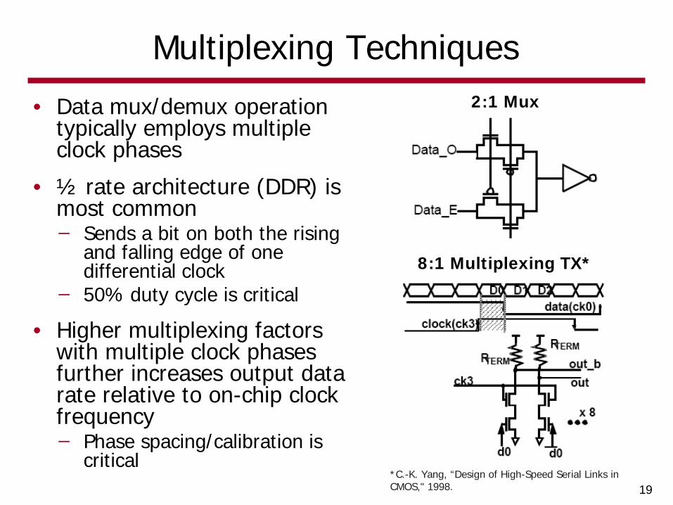
Multiplexing Techniques
• Data mux/demux operation typically employs multiple clock phases
• ½ rate architecture (DDR) is most common Sends a bit on both the rising
and falling edge of one differential clock
50% duty cycle is critical
• Higher multiplexing factors with multiple clock phases further increases output data rate relative to on-chip clock frequency Phase spacing/calibration is
critical
2:1 Mux
8:1 Multiplexing TX*
*C.-K. Yang, “Design of High-Speed Serial Links in CMOS," 1998.

20
Current vs Voltage-Mode Driver
• Signal integrity considerations (min. reflections) requires 50Ω driver output impedance
• To produce an output drive voltage Current-mode drivers use Norton-equivalent parallel termination
• Easier to control output impedance Voltage-mode drivers use Thevenin-equivalent series termination
• Potentially ½ to ¼ the current for a given output swing
D+
D-
2VSWVZcont
D+
D-
Current-Mode Voltage-Mode
21
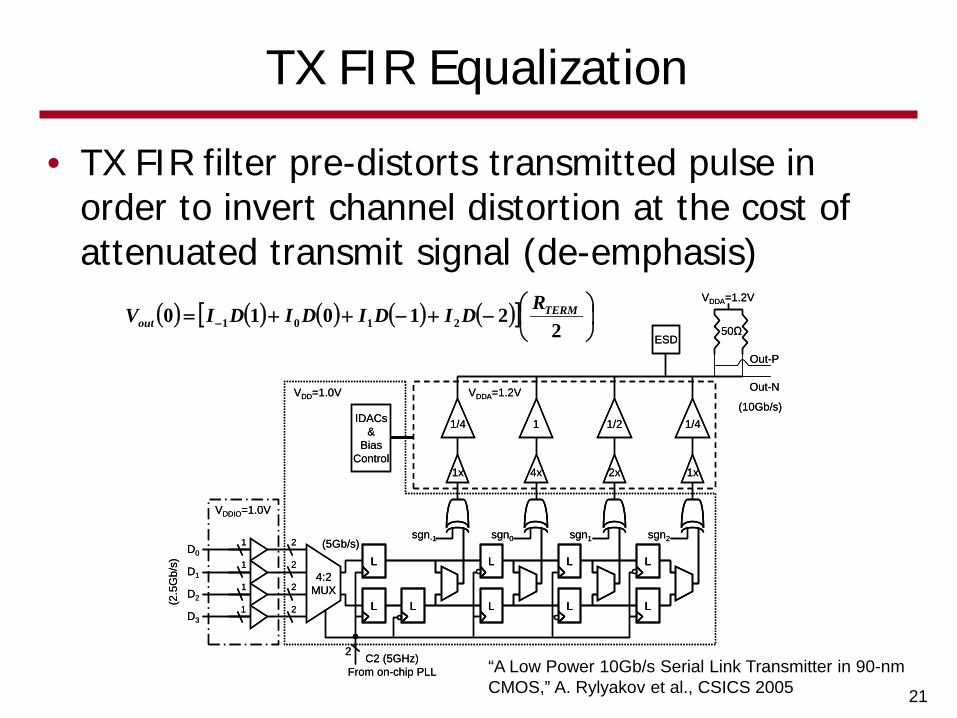
TX FIR Equalization
• TX FIR filter pre-distorts transmitted pulse in order to invert channel distortion at the cost of attenuated transmit signal (de-emphasis)
L
L L
L
L
L
L
L
L
1x 4x 2x 1x
1/4 1 1/2 1/4IDACs&
BiasControl
sgn-1 sgn0 sgn1 sgn2
50Ω
Out-P
Out-N
4:2MUX
2
2
2
21
D0
D1
D2
D3
VDDA=1.2VVDD=1.0V
VDDIO=1.0V
VDDA=1.2V
1
1
1
C2 (5GHz)From on-chip PLL
2
(2.5
Gb/
s)
(10Gb/s)
(5Gb/s)
ESD
L
L L
L
L
L
L
L
L
LL
LL LL
LL
LL
LL
LL
LL
LL
1x 4x 2x 1x
1/4 1 1/2 1/4IDACs&
BiasControl
sgn-1 sgn0 sgn1 sgn2
50Ω
Out-P
Out-N
4:2MUX
2
2
2
21
D0
D1
D2
D3
VDDA=1.2VVDD=1.0V
VDDIO=1.0V
VDDA=1.2V
1
1
1
C2 (5GHz)From on-chip PLL
2
(2.5
Gb/
s)
(10Gb/s)
(5Gb/s)
ESD
( ) ( ) ( ) ( ) ( )[ ]
−+−++= − 2
21010 2101TERM
outRDIDIDIDIV
“A Low Power 10Gb/s Serial Link Transmitter in 90-nm CMOS,” A. Rylyakov et al., CSICS 2005

22
6Gb/s TX FIR Equalization Example
• Pros Simple to implement Can cancel ISI in pre-
cursor and beyond filter span
Doesn’t amplify noise Can achieve 5-6bit
resolution
• Cons Attenuates low
frequency content due to peak-power limitation
Need a “back-channel” to tune filter taps
23
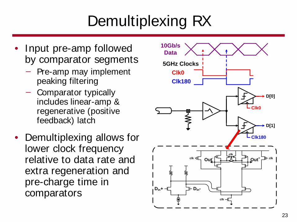
Demultiplexing RX
• Input pre-amp followed by comparator segments Pre-amp may implement
peaking filtering Comparator typically
includes linear-amp & regenerative (positive feedback) latch
• Demultiplexing allows for lower clock frequency relative to data rate and extra regeneration and pre-charge time in comparators
Clk0Clk180
10Gb/s Data
5GHz Clocks
Clk0
Clk180
D[0]
D[1]
Out+Out-
clk
clk clkclk
Din-Din+
24
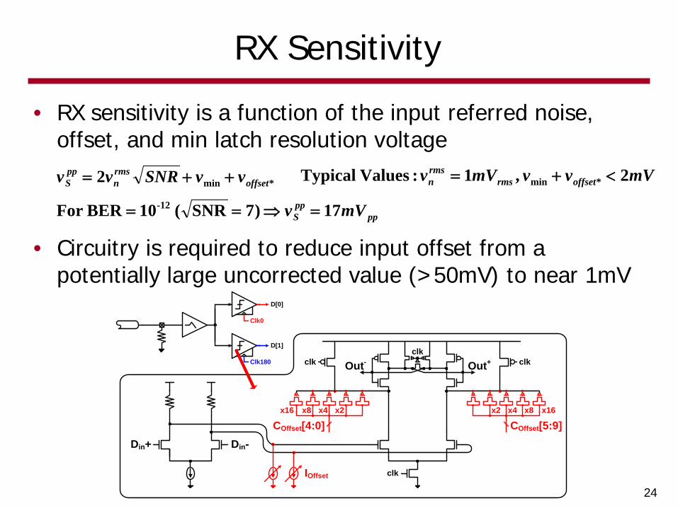
RX Sensitivity
• RX sensitivity is a function of the input referred noise, offset, and min latch resolution voltage
Out+Out-
x2x4x8x16
COffset[4:0]x2 x4 x8 x16
COffset[5:9]
clk
clk clkclk
Din-Din+
IOffset
Clk0
Clk180
D[0]
D[1]
• Circuitry is required to reduce input offset from a potentially large uncorrected value (>50mV) to near 1mV
*min2 offsetrmsn
ppS vvSNRvv ++= mVvvmVv offsetrms
rmsn 2 ,1 :Values Typical *min <+=
17)7SNR( 10BERFor -12pp
ppS mVv =⇒==

25
RX Equalization #1: RX FIR
• Pros With sufficient dynamic range, can amplify
high frequency content (rather than attenuate low frequencies)
Can cancel ISI in pre-cursor and beyond filter span
Filter tap coefficients can be adaptively tuned without any back-channel
• Cons Amplifies noise/crosstalk Implementation of analog delays Tap precision
w-1
z-1
x w0
z-1
x
z-1
x wn-1
z-1
wnx
Σ DEQ
Din
Analog Delay Elements
*
*D. Hernandez-Garduno and J. Silva-Martinez, “A CMOS 1Gb/s 5-Tap Transversal Equalizer based on 3rd-Order Delay Cells," ISSCC, 2007.

26
RX Equalization #2: RX CTLE
Din- Din+
Vo-Vo+
• Pros Provides gain and
equalization with low power and area overhead
Can cancel both pre-cursor and long-tail ISI
• Cons Generally limited to 1st
order compensation Amplifies noise/crosstalk PVT sensitivity Can be hard to tune

27
RX Equalization #3: RX DFE
z-1clk
Σ
x
w1
z-1x
w2
z-1x
wn-1
z-1x
wn
Din DRX
• Pros No noise and crosstalk
amplification Filter tap coefficients
can be adaptively tuned without any back-channel
• Cons Cannot cancel pre-
cursor ISI Critical feedback timing
path Timing of ISI
subtraction complicates CDR phase detection
28
Outline
• Introduction
• Electrical I/O Overview Channel characteristics Transmitter & receiver circuits Clocking techniques & circuits
• Future trends & optical I/O
• Conclusion
29
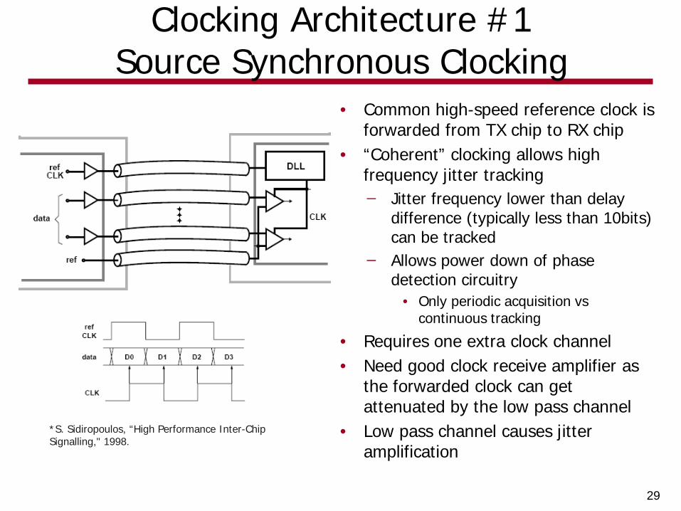
Clocking Architecture #1Source Synchronous Clocking
• Common high-speed reference clock is forwarded from TX chip to RX chip
• “Coherent” clocking allows high frequency jitter tracking Jitter frequency lower than delay
difference (typically less than 10bits) can be tracked
Allows power down of phase detection circuitry
• Only periodic acquisition vs continuous tracking
• Requires one extra clock channel• Need good clock receive amplifier as
the forwarded clock can get attenuated by the low pass channel
• Low pass channel causes jitter amplification
*S. Sidiropoulos, “High Performance Inter-Chip Signalling," 1998.
30
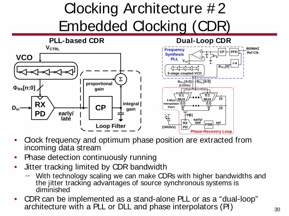
• Clock frequency and optimum phase position are extracted from incoming data stream
• Phase detection continuously running• Jitter tracking limited by CDR bandwidth
With technology scaling we can make CDRs with higher bandwidths and the jitter tracking advantages of source synchronous systems is diminished
• CDR can be implemented as a stand-alone PLL or as a “dual-loop” architecture with a PLL or DLL and phase interpolators (PI)
Clocking Architecture #2Embedded Clocking (CDR)
early/late
RXPD
CP
Σ
VCTRL
integral gain
proportional gain
VCO
Din
Loop Filter
ΦRX[n:0]
FSM selearly/late
Phase-Recovery Loop
RXPD
Ψ[4:0]
CP
Vctrl
FrequencySynthesis
PLL
5-stage coupled VCO
4
800MHZ Ref ClkPFD
ΦPLL[4:0]
(16Gb/s)
5 Mux/Interpolator
Pairs
5:1 MUX
5:1 MUX
ΦPLL[4:0](3.2GHz)
ΦPLL[0]
15
10
PLL-based CDR Dual-Loop CDR

31
• Used for frequency synthesis at TX and embedded-clocked RX• Second/third order loop
Charge pump & integrating loop filter produces voltage to control VCO frequency
Output phase is integration of VCO frequency Zero required in loop filter for stability
• Low-noise VCO (or high BW PLL) required to minimize jitter accumulation
Phase-Locked Loop (PLL)
*J. Bulzacchelli et al, “A 10Gb/s 5Tap DFE/4Tap FFE Transceiver in 90nm CMOS Technology," JSSC, 2006.

32
Delay-Locked Loop (DLL)
• Typically used to generate multiple clock phases in RX• First order loop guarantees stability• Delay line doesn’t accumulate jitter like a VCO• Difficult to use for frequency synthesis
0º 210º 60º 270º 120º 330º 180º
33
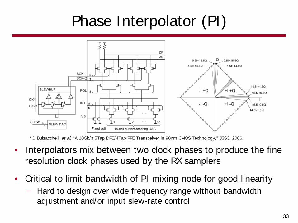
• Interpolators mix between two clock phases to produce the fine resolution clock phases used by the RX samplers
• Critical to limit bandwidth of PI mixing node for good linearity Hard to design over wide frequency range without bandwidth
adjustment and/or input slew-rate control
Phase Interpolator (PI)
*J. Bulzacchelli et al, “A 10Gb/s 5Tap DFE/4Tap FFE Transceiver in 90nm CMOS Technology," JSSC, 2006.

34
Clock Distribution
Architecture Jitter Power Area Complexity
Inverter Moderate Moderate Low Low
CML Good High Moderate Moderate
T-line Good Low Low ModerateResonant T-line Excellent Low High High
*J. Poulton et al, “A 14mW 6.25Gb/s Transceiver in 90nm CMOS," JSSC, 2007.
• Careful clock distribution is required in multi-channel I/O systems
• Different distribution architectures trade-off jitter, power, area, and complexity
Resonant T-line DistributionExample

35
Outline
• Introduction
• Electrical I/O Overview Channel characteristics Transmitter & receiver circuits Clocking techniques & circuits
• Future trends & optical I/O
• Conclusion
36
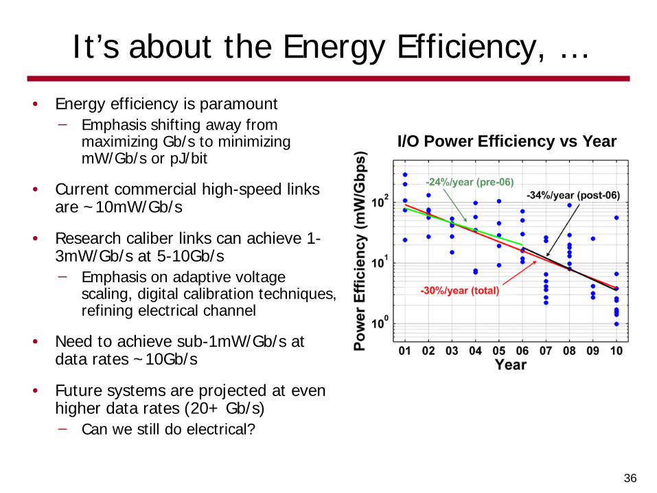
It’s about the Energy Efficiency, …• Energy efficiency is paramount
Emphasis shifting away from maximizing Gb/s to minimizing mW/Gb/s or pJ/bit
• Current commercial high-speed links are ~10mW/Gb/s
• Research caliber links can achieve 1-3mW/Gb/s at 5-10Gb/s Emphasis on adaptive voltage
scaling, digital calibration techniques, refining electrical channel
• Need to achieve sub-1mW/Gb/s at data rates ~10Gb/s
• Future systems are projected at even higher data rates (20+ Gb/s) Can we still do electrical?
I/O Power Efficiency vs Year

37
Other Trends
• Can we do better than simple NRZ modulation? Multi-level (4/8-PAM) Multi-tone Duo-binary
• Active crosstalk cancellation Package constraints require high density and high data rate
• ADC-based RX front-ends Get to digital ASAP Allows improved SNR front-ends, but probably doesn’t save
power
38
negligible frequency dependent lossnegligible frequency dependent loss
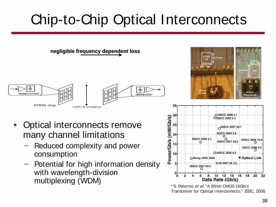
Chip-to-Chip Optical Interconnects
• Optical interconnects remove many channel limitations Reduced complexity and power
consumption Potential for high information density
with wavelength-division multiplexing (WDM)
*S. Palermo et al, “A 90nm CMOS 16Gb/s Transceiver for Optical Interconnects," JSSC, 2008.
39
Conclusion
• High-speed I/O systems offer challenges in both circuit and communication system design High-speed TX/RX, low jitter clocking, and efficient
equalizer circuits
• Key issue with scaling high-speed I/O is meeting the energy efficiency targets required by future systems (→1mW/Gb/s) Requires circuit improvements and constant electrical
channel refinement Optical I/O is a major candidate in this space

40
Interested In Research In This Area?
• Graduate Students Take the 689 class
• Undergraduate Students Opportunities exist for undergraduate research
credits (491)