ece 663 mosfet scaling. ece 663 scaling of switches
TRANSCRIPT
ECE 663
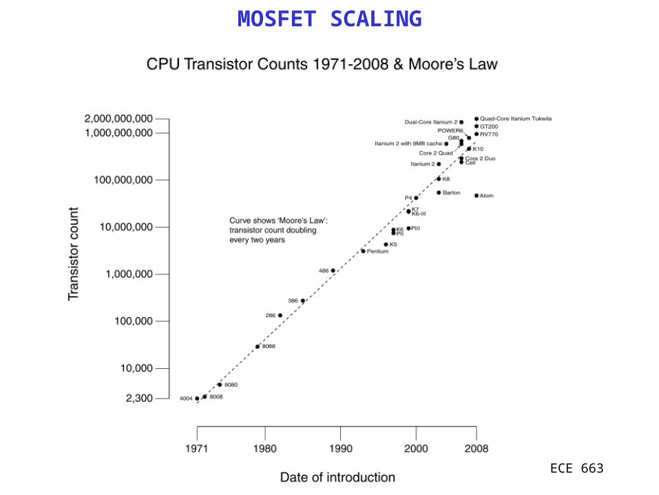
MOSFET SCALING
ECE 663
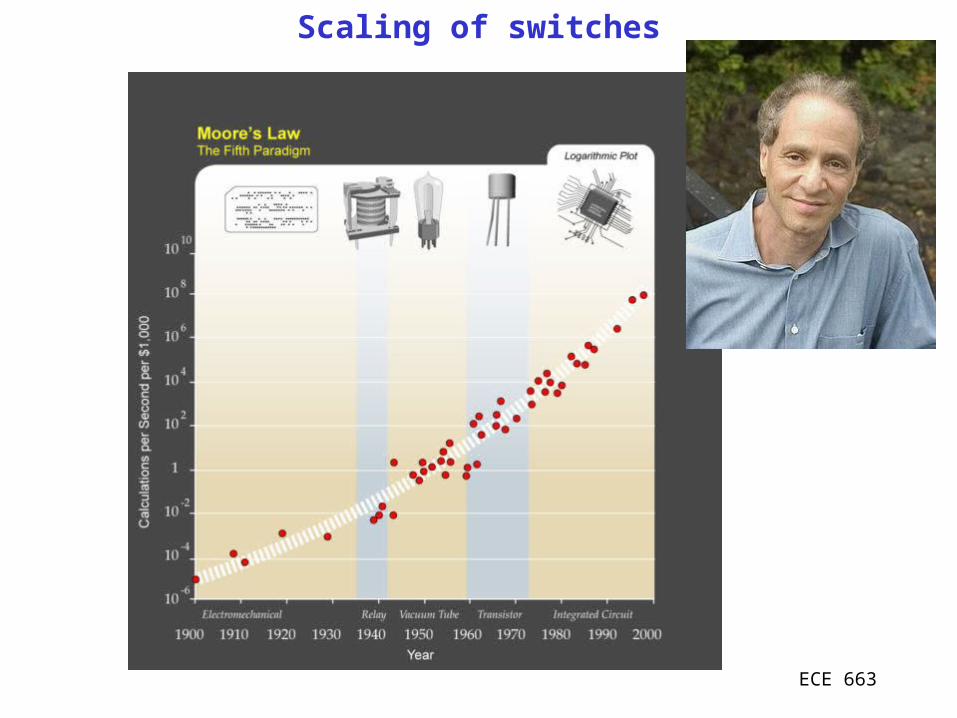
Scaling of switches
ECE 663
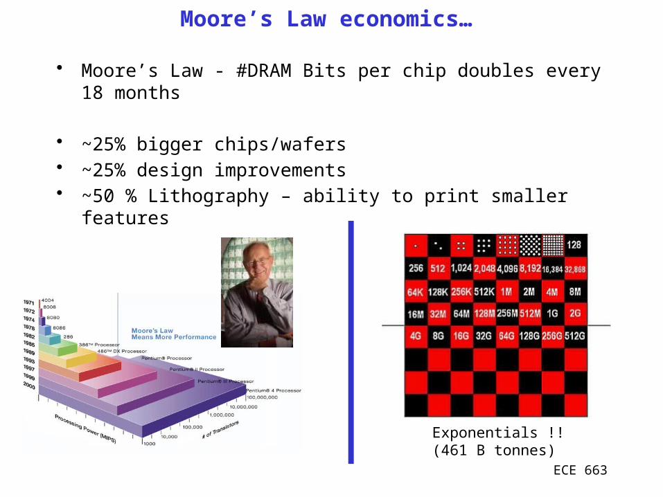
Moore’s Law economics…
• Moore’s Law - #DRAM Bits per chip doubles every 18 months
• ~25% bigger chips/wafers• ~25% design improvements• ~50 % Lithography – ability to print smaller features
Exponentials !!(461 B tonnes)
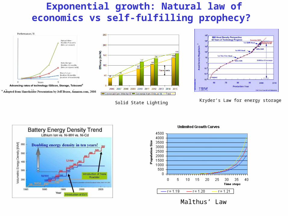
Exponential growth: Natural law of economics vs self-fulfilling prophecy?
Kryder’s Law for energy storage
Malthus’ Law
Solid State Lighting
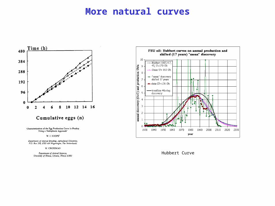
More natural curves
Hubbert Curve
ECE 663
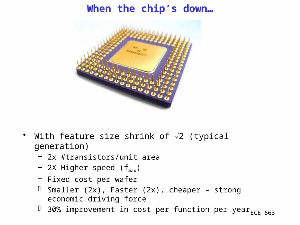
When the chip’s down…
• With feature size shrink of 2 (typical generation)– 2x #transistors/unit area– 2X Higher speed (fmax)– Fixed cost per waferÞ Smaller (2x), Faster (2x), cheaper – strong economic
driving forceÞ 30% improvement in cost per function per year
ECE 663
ECE 663
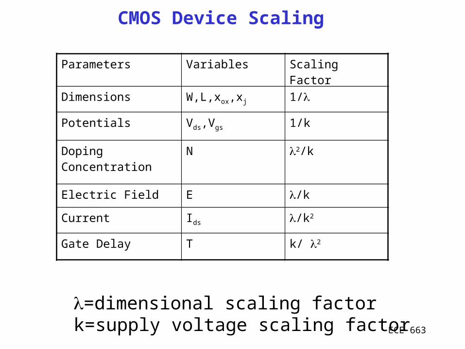
CMOS Device Scaling
Parameters Variables Scaling Factor
Dimensions W,L,xox,xj 1/
Potentials Vds,Vgs 1/k
Doping Concentration N 2/k
Electric Field E /k
Current Ids /k2
Gate Delay T k/ 2
=dimensional scaling factork=supply voltage scaling factor
ECE 663
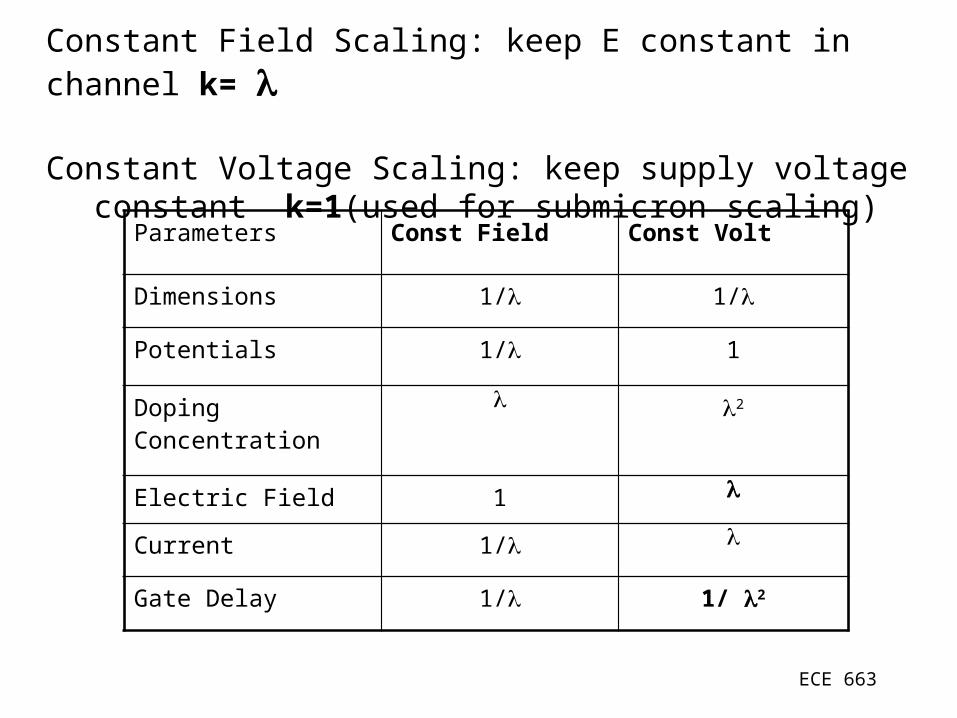
Constant Field Scaling: keep E constant in channel k=
Constant Voltage Scaling: keep supply voltage constant k=1(used for submicron scaling)
Parameters Const Field Const Volt
Dimensions 1/ 1/
Potentials 1/ 1
Doping Concentration 2
Electric Field 1
Current 1/
Gate Delay 1/ 1/ 2
ECE 663
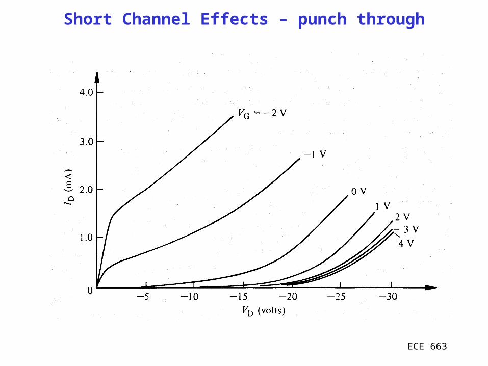
Short Channel Effects – punch through
ECE 663
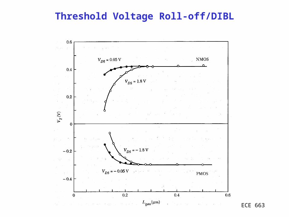
Threshold Voltage Roll-off/DIBL
ECE 663
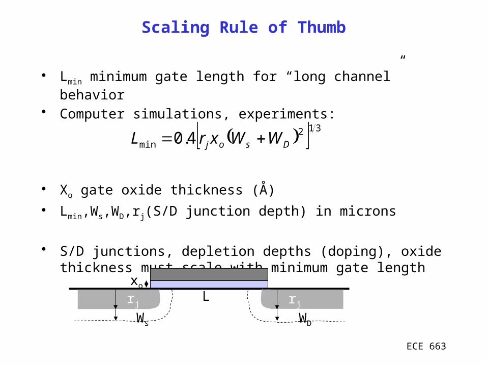
Scaling Rule of Thumb
• Lmin minimum gate length for “long channel” behavior• Computer simulations, experiments:
• Xo gate oxide thickness (Å)
• Lmin,Ws,WD,rj(S/D junction depth) in microns
• S/D junctions, depletion depths (doping), oxide thickness must scale with minimum gate length
312min 4.0 Dsoj WWxrL
rj
Ws
xo
rj
WD
L
ECE 663
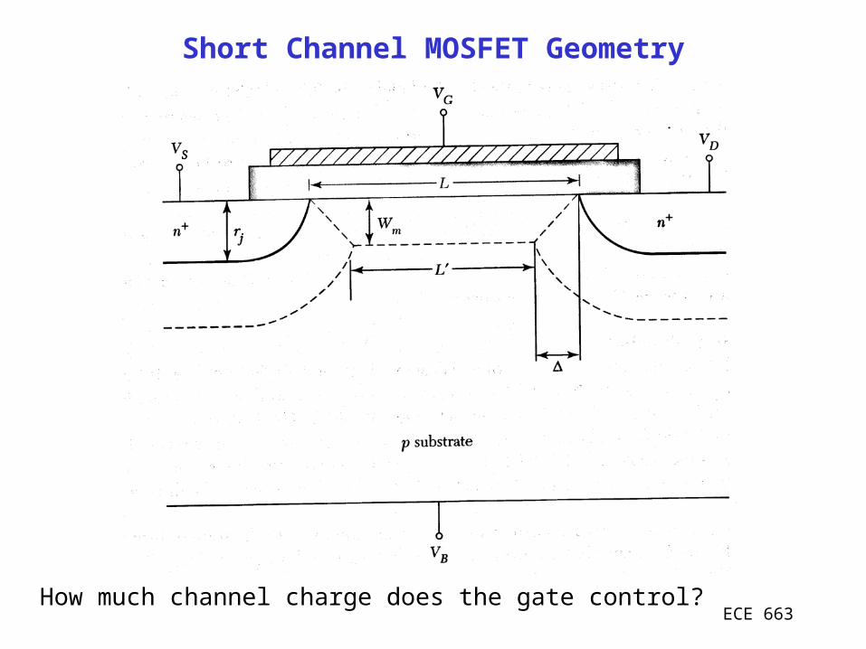
Short Channel MOSFET Geometry
How much channel charge does the gate control?
ECE 663
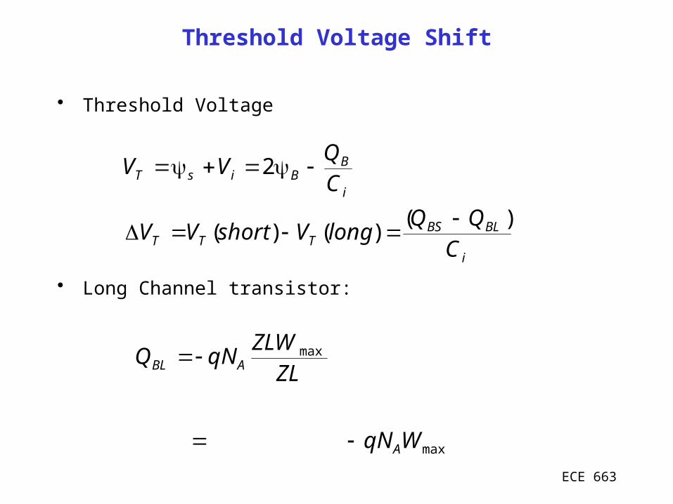
Threshold Voltage Shift
• Threshold Voltage
• Long Channel transistor:
i
BLBSTTT
i
BBisT
CQQ
longVshortVV
CQ
VV
)()()(
2
maxmax WqN
ZLZLW
qNQ AABL
maxmax WqN
ZLZLW
qNQ AABL
ECE 663
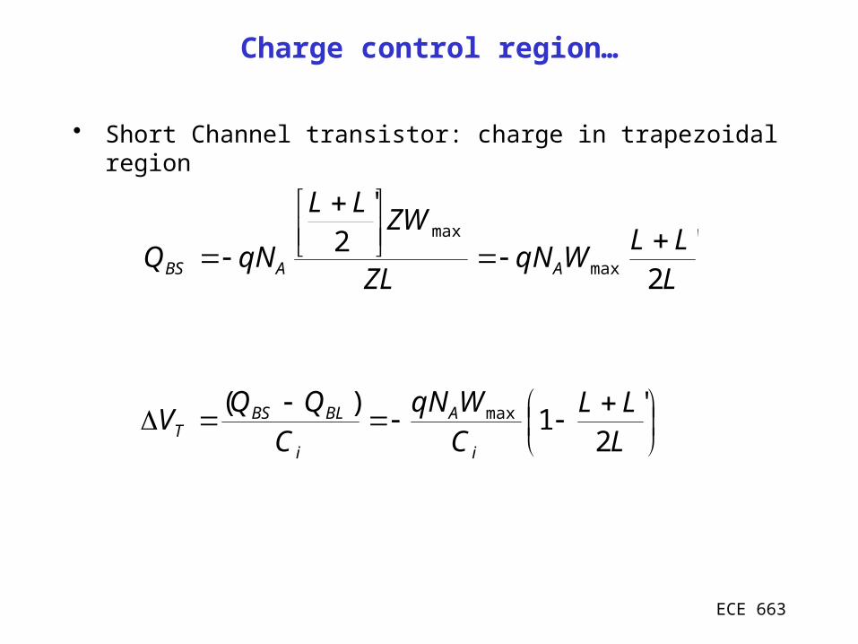
• Short Channel transistor: charge in trapezoidal region
LLL
WqNZL
ZWLL
qNQ AABS 2'2
'
max
max
LLL
CWqN
CQQ
Vi
A
i
BLBST 2
'1
)( max
Charge control region…
ECE 663
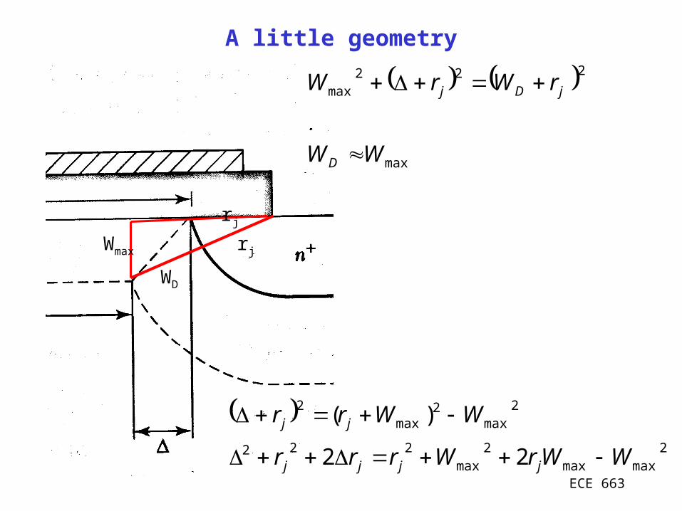
A little geometry
rj
WD
Wmax
rj
max
222max
WW
rWrW
D
jDj
2
maxmax2
max222
2max
2max
2
22
)(
WWrWrrr
WWrr
jjjj
jj
ECE 663
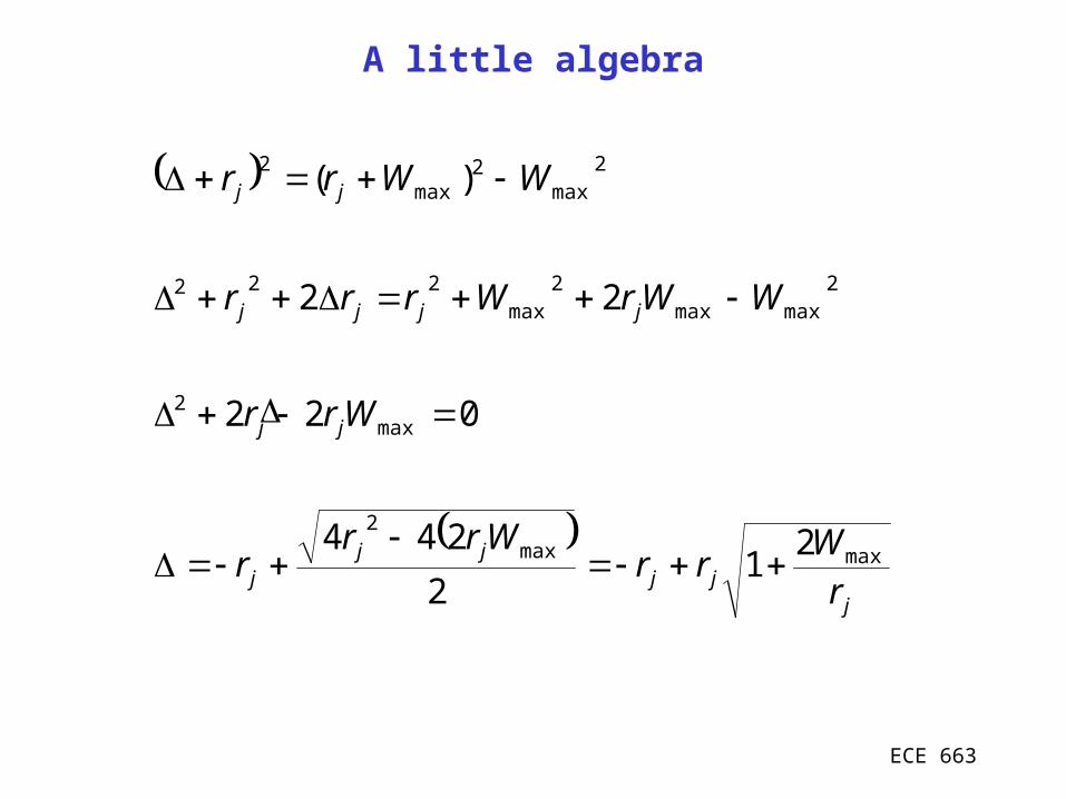
A little algebra
j
jjjj
j
jj
jjjj
jj
rW
rrWrr
r
Wrr
WWrWrrr
WWrr
maxmax2
max2
2maxmax
2max
222
2max
2max
2
21
2
244
022
22
)(
ECE 663
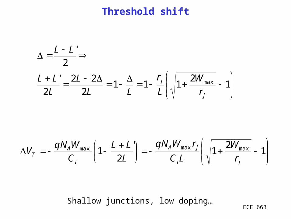
Threshold shift
12
1112
222
'
2'
max
j
j
rW
L
r
LLL
LLL
LL
1
21
2'
1 maxmaxmax
ji
jA
i
AT r
WLC
rWqN
LLL
CWqN
V
Shallow junctions, low doping…
ECE 663
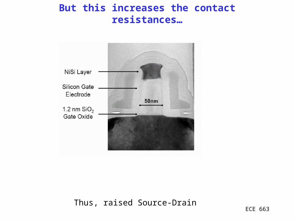
But this increases the contact resistances…
Thus, raised Source-Drain
ECE 663
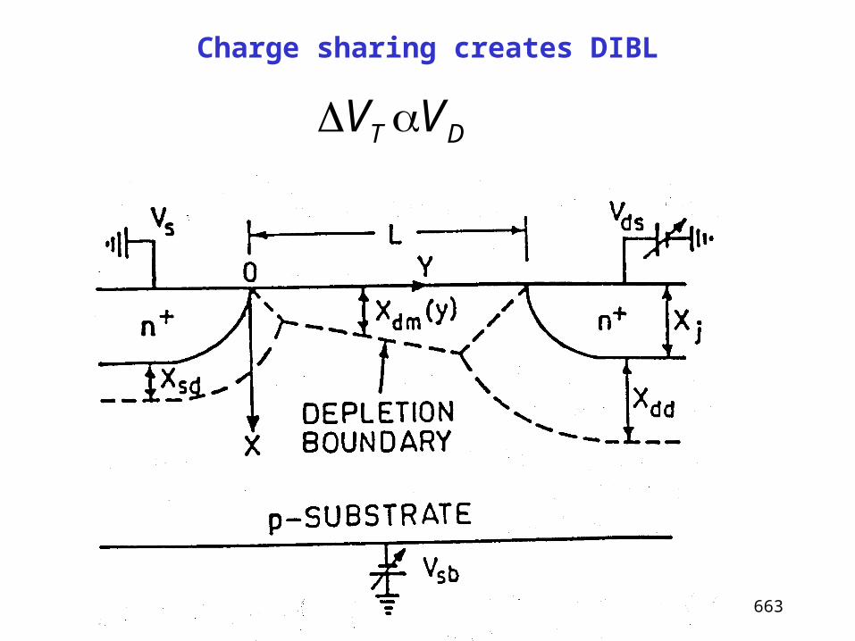
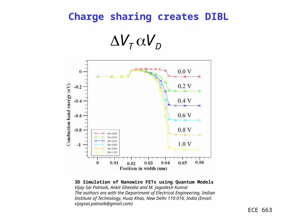
Charge sharing creates DIBL
DT VV
ECE 663
Charge sharing creates DIBL
DT VV
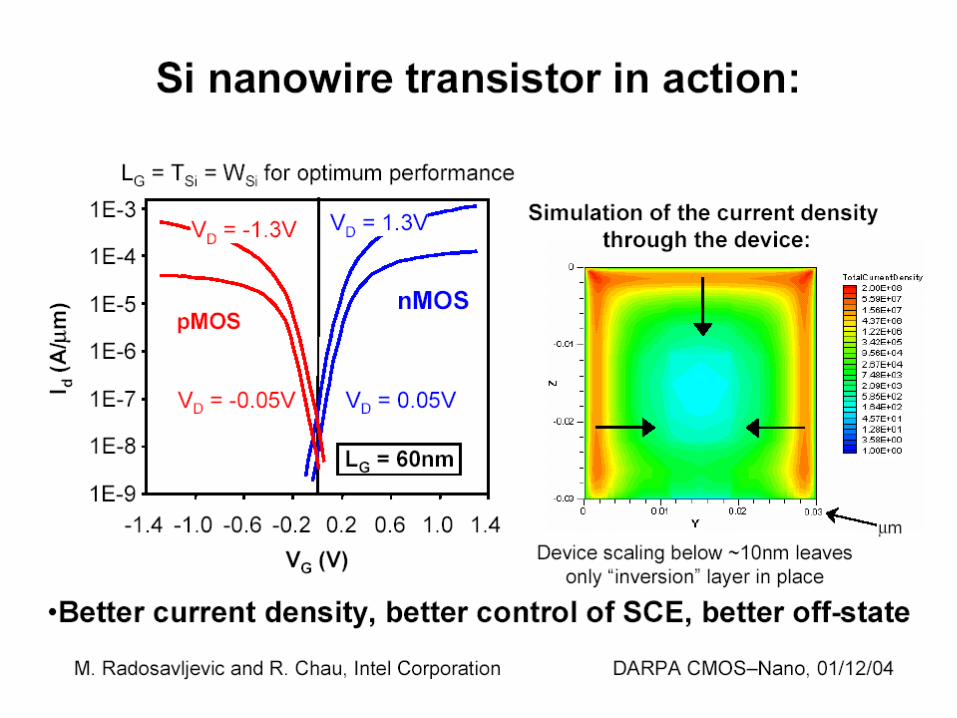
3D Simulation of Nanowire FETs using Quantum Models Vijay Sai Patnaik, Ankit Gheedia and M. Jagadesh KumarThe authors are with the Department of Electrical Engineering, Indian Institute of Technology, Huaz Khas, New Delhi 110 016, India (Email: [email protected])
ECE 663
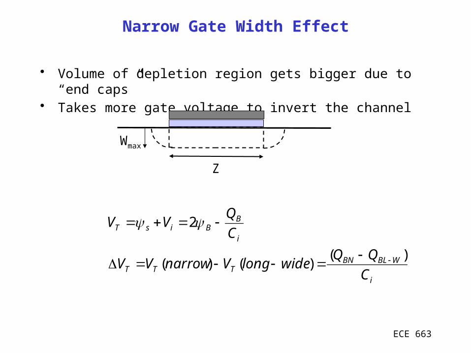
Narrow Gate Width Effect
• Volume of depletion region gets bigger due to “end caps”
• Takes more gate voltage to invert the channel
Wmax
i
WBLBNTTT
i
BBisT
C
QQwidelongVnarrowVV
C
QVV
)()()(
2
Z
ECE 663
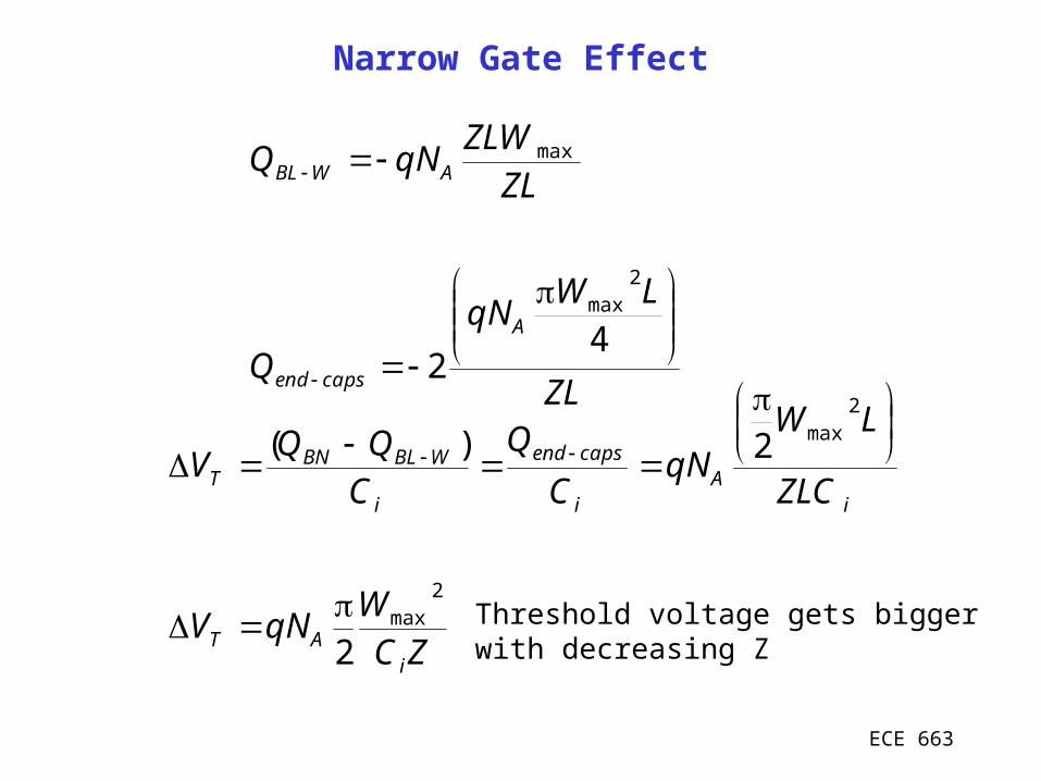
Narrow Gate Effect
ZL
LWqN
Q
ZLZLW
qNQ
A
capsend
AWBL
42
2max
max
ZCW
qNV
ZLC
LWqN
C
Q
CQQ
V
iAT
iA
i
capsend
i
WBLBNT
2max
2max
2
2)(
Threshold voltage gets biggerwith decreasing Z
ECE 663
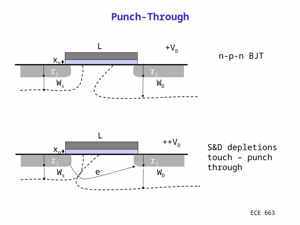
Punch-Through
rj
Ws
xo
rj
WD
L
rj
Ws
xo
rj
WD
L
+VD
++VD
n-p-n BJT
S&D depletions touch – punch throughe-
ECE 663
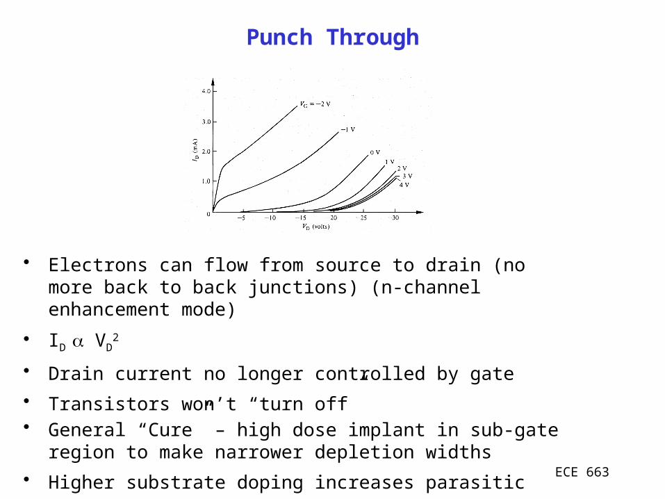
Punch Through
• Electrons can flow from source to drain (no more back to back junctions) (n-channel enhancement mode)
• ID VD2
• Drain current no longer controlled by gate
• Transistors won’t “turn off”• General “Cure” – high dose implant in sub-gate region
to make narrower depletion widths
• Higher substrate doping increases parasitic capacitances
ECE 663
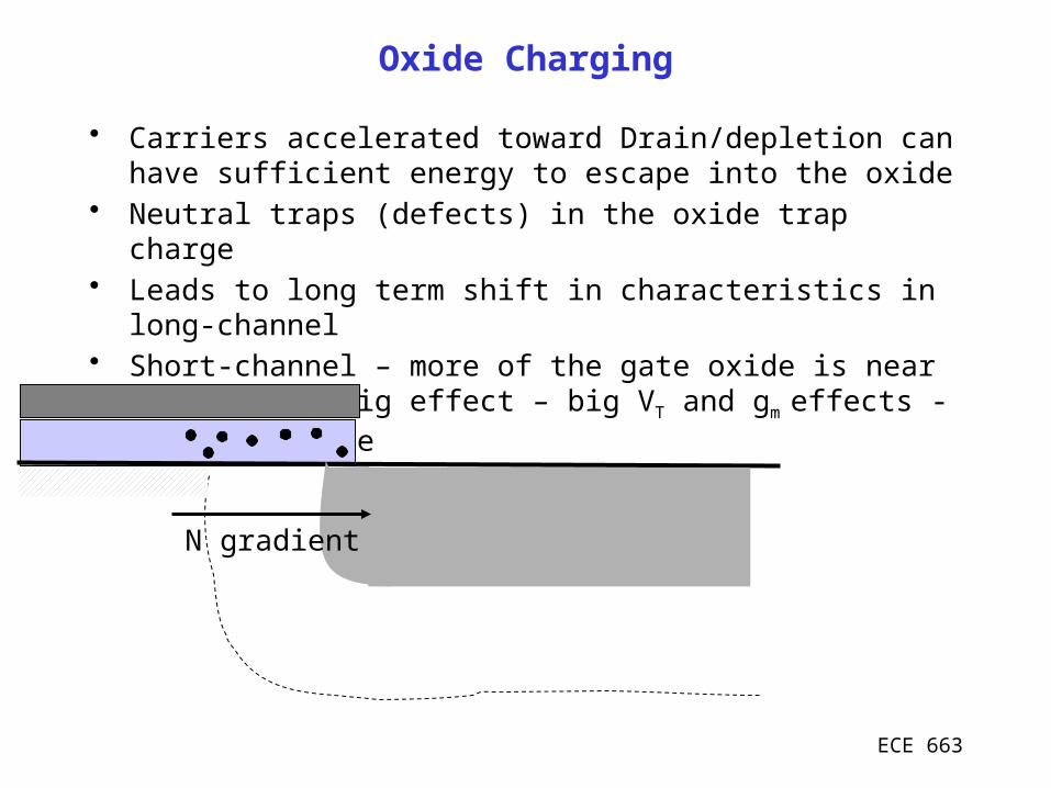
Oxide Charging
• Carriers accelerated toward Drain/depletion can have sufficient energy to escape into the oxide
• Neutral traps (defects) in the oxide trap charge• Leads to long term shift in characteristics in long-
channel• Short-channel – more of the gate oxide is near the drain
– big effect – big VT and gm effects - device failure
N gradient
ECE 663
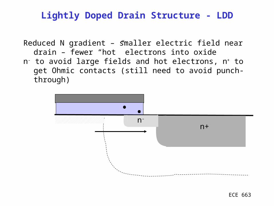
Lightly Doped Drain Structure - LDD
Reduced N gradient – smaller electric field near drain – fewer “hot” electrons into oxide
n- to avoid large fields and hot electrons, n+ to get Ohmic contacts (still need to avoid punch-through)
n-
n+
ECE 663
Lightly Doped Drain Structure - LDD
Reduced N gradient – smaller electric field near drain – fewer “hot” electrons into oxide
n- to avoid large fields and hot electrons, n+ to get Ohmic contacts
n-
n+
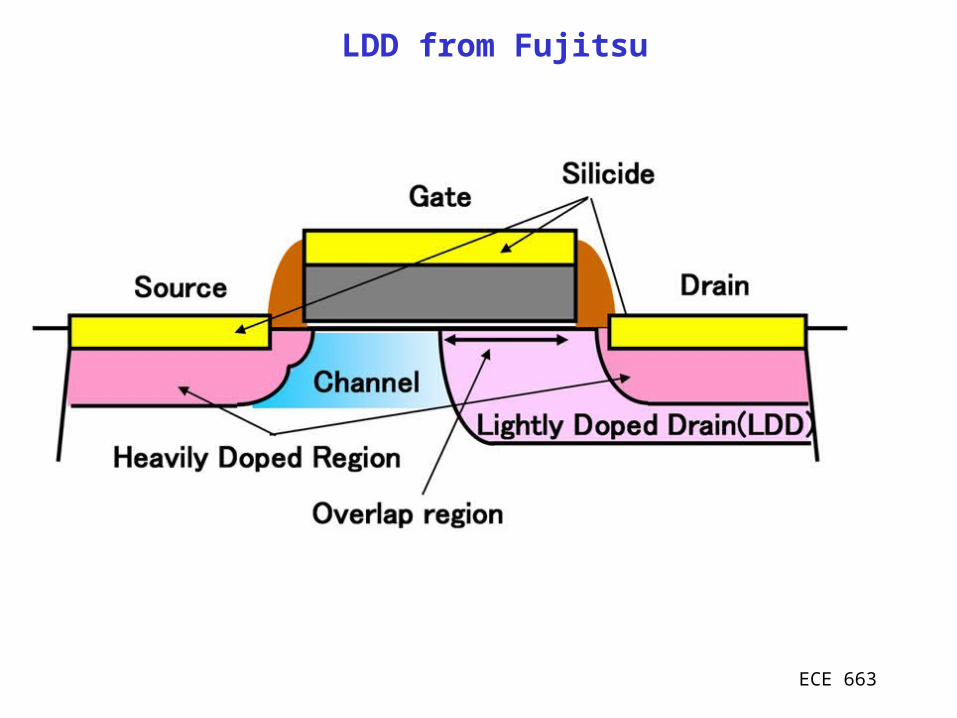
LDD from Fujitsu
ECE 663
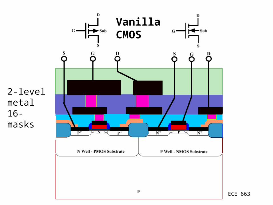
VanillaCMOS
2-level metal16-masks
ECE 663
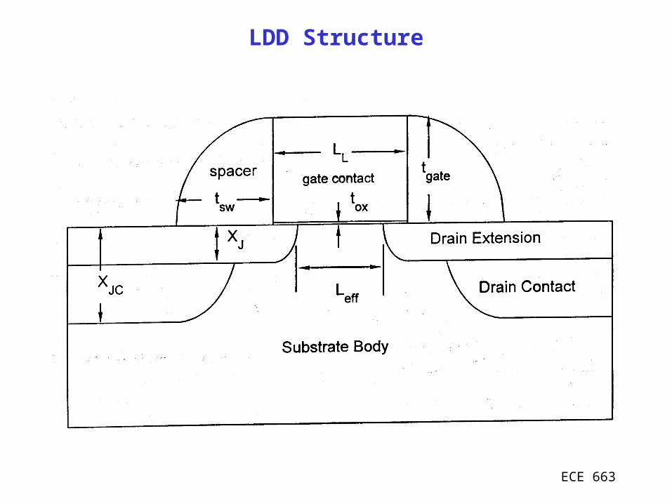
LDD Structure
ECE 663
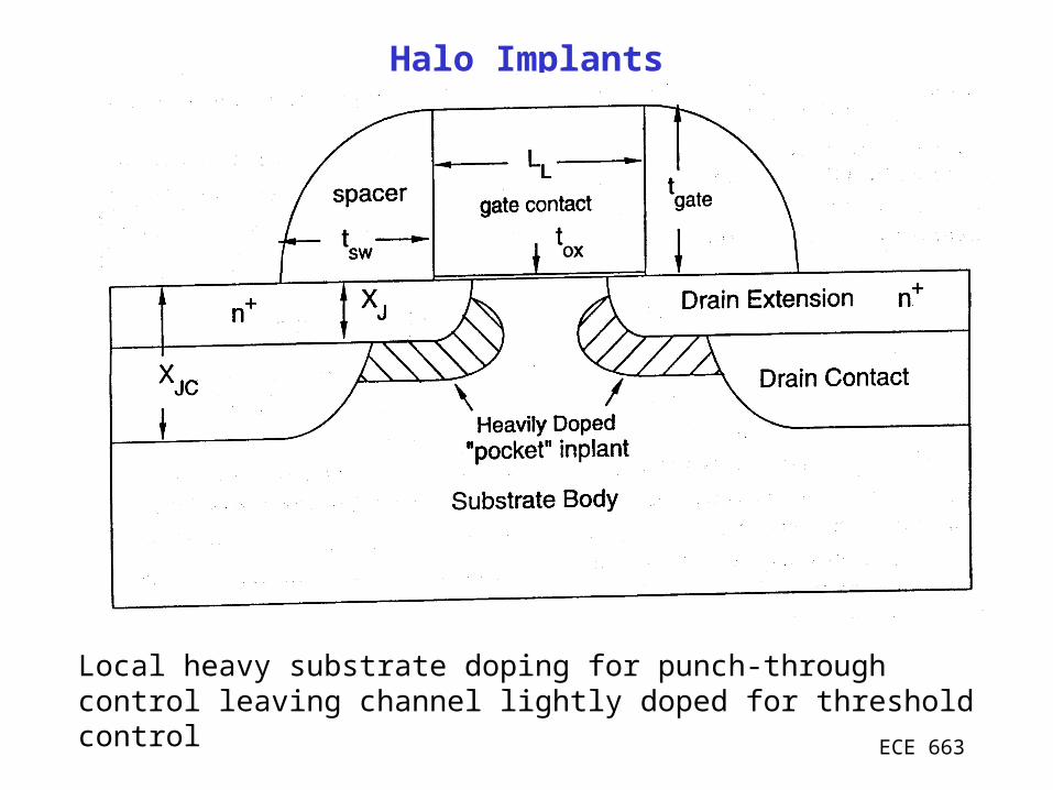
Halo Implants
Local heavy substrate doping for punch-through control leaving channel lightly doped for threshold control
ECE 663
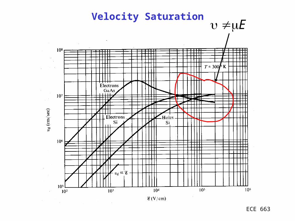
Velocity SaturationE
ECE 663
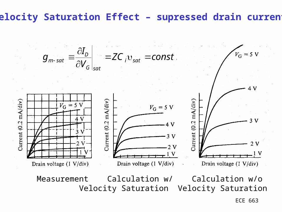
Velocity Saturation Effect – supressed drain current
Measurement Calculation w/ Calculation w/oVelocity Saturation Velocity Saturation
.constZCVI
g sati
satG
Dsatm
ECE 663
ECE 663
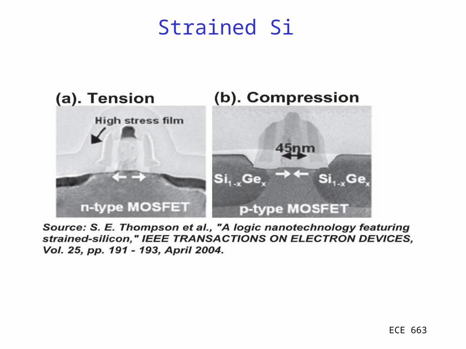
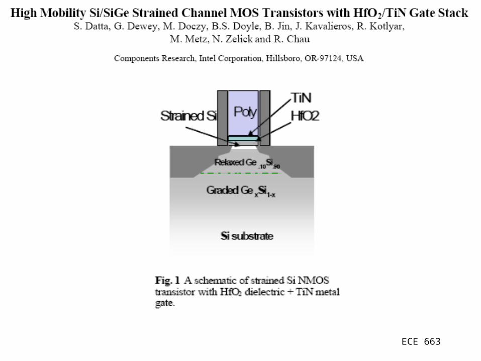
Strained Si
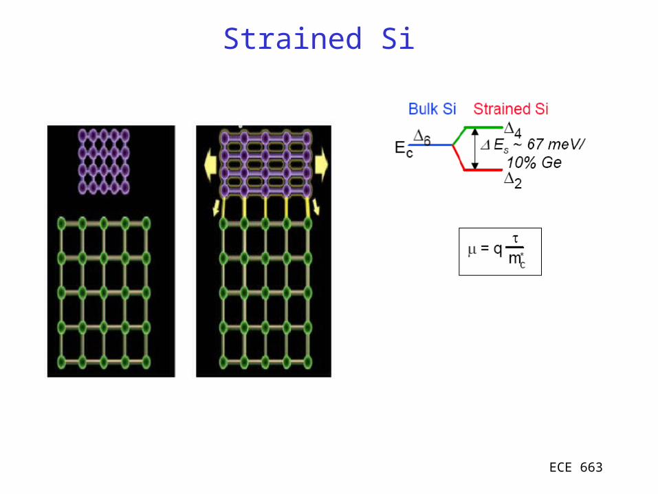
ECE 663
Strained Si
ECE 663
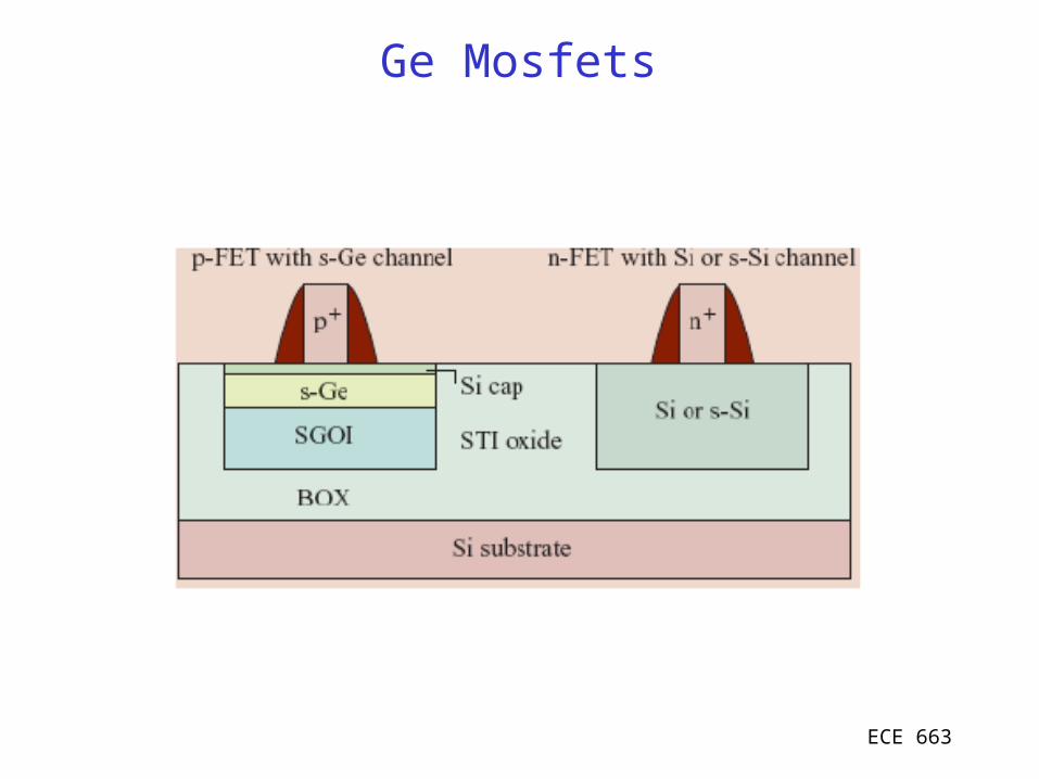
Ge Mosfets
ECE 663
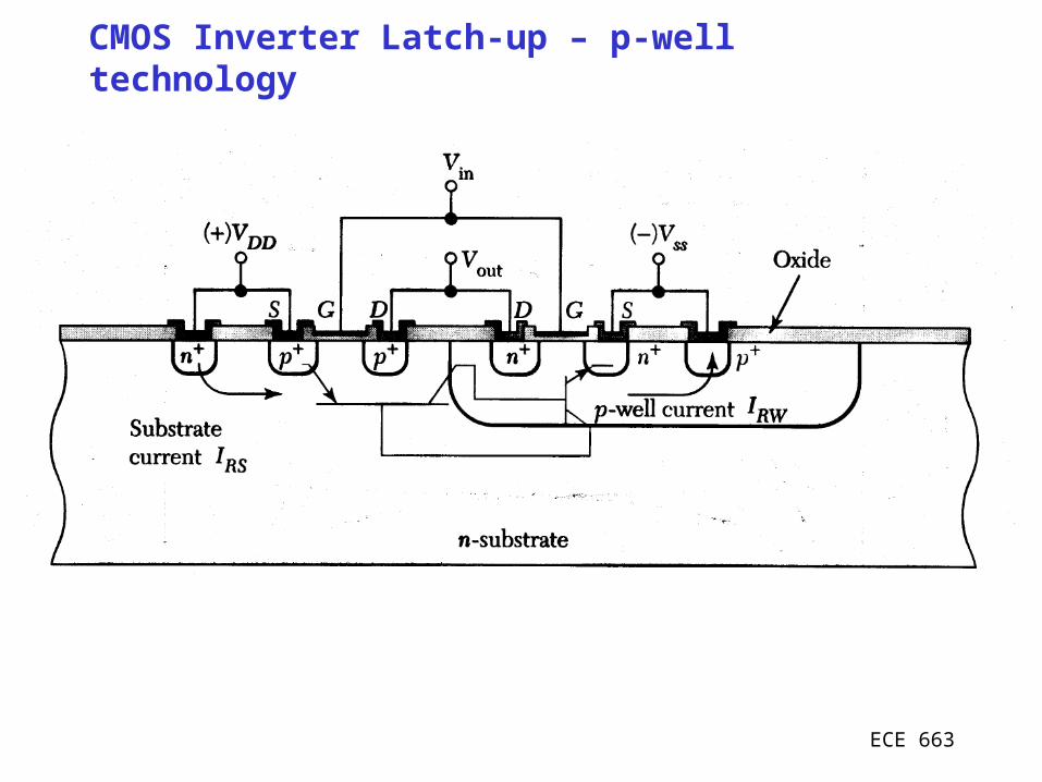
CMOS Inverter Latch-up – p-well technology
ECE 663
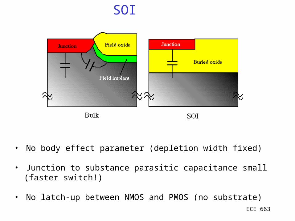
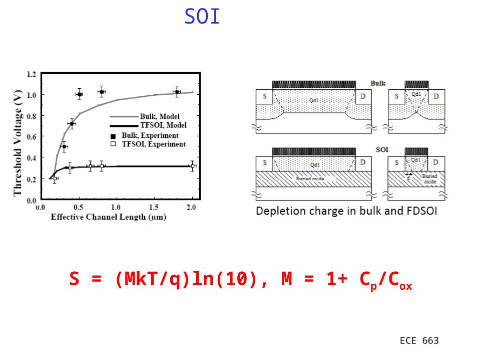
SOI
• No body effect parameter (depletion width fixed)
• Junction to substance parasitic capacitance small (faster switch!)
• No latch-up between NMOS and PMOS (no substrate)
ECE 663
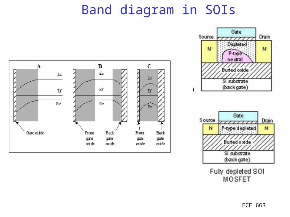
Band diagram in SOIs
ECE 663
SOI
S = (MkT/q)ln(10), M = 1+ Cp/Cox
ECE 663
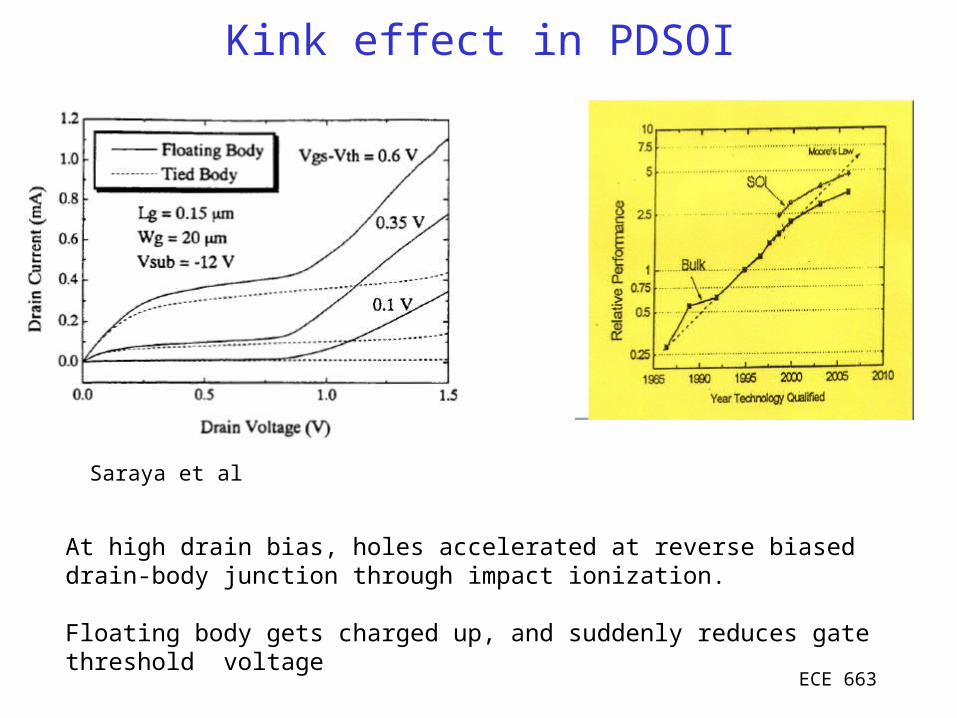
Kink effect in PDSOI
At high drain bias, holes accelerated at reverse biased drain-body junction through impact ionization.
Floating body gets charged up, and suddenly reduces gate threshold voltage
Saraya et al
ECE 663
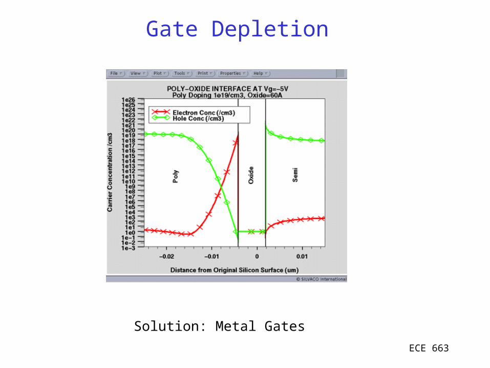
Gate Depletion
Solution: Metal Gates
ECE 663
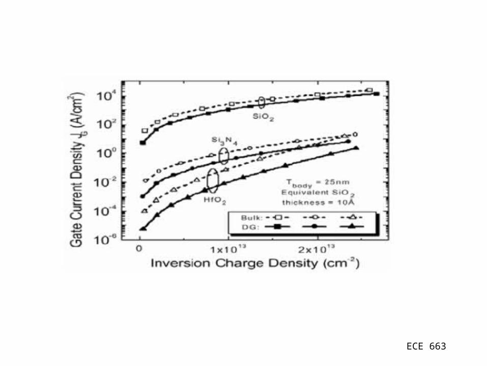
ECE 663
ECE 663
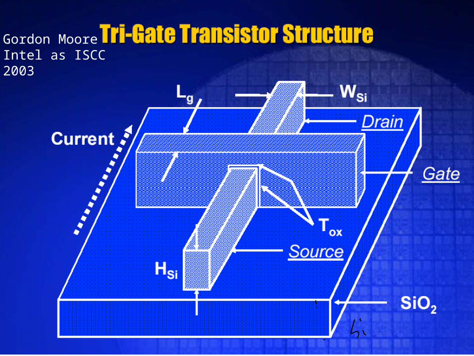
Gordon MooreIntel as ISCC2003
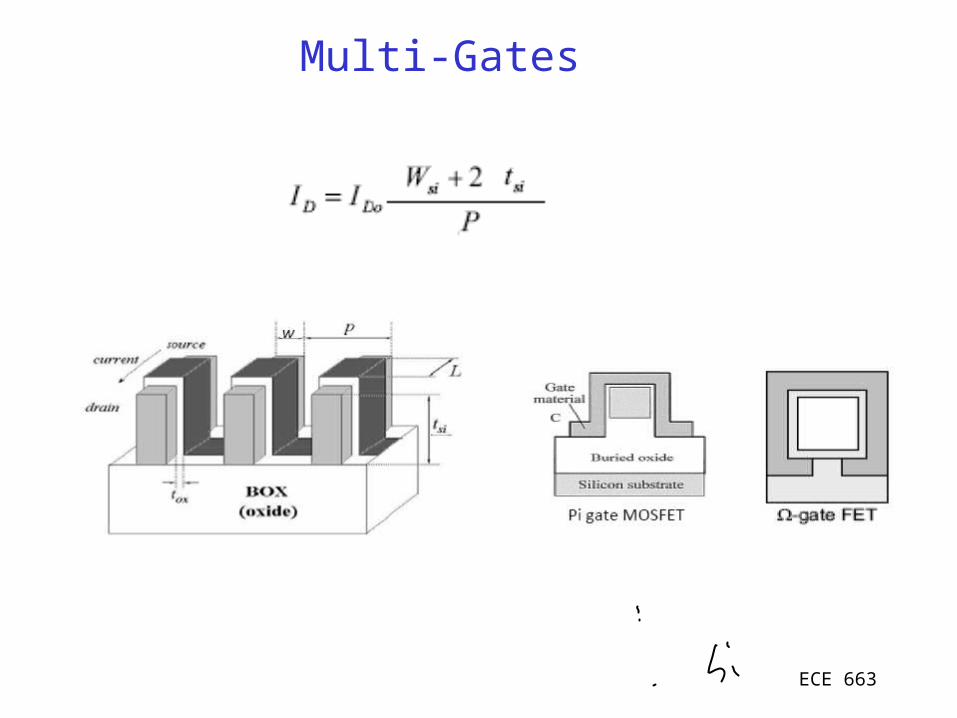
Multi-Gates
ECE 663
Gordon MooreIntel as ISCC2003
ECE 663