ece 663 ac diode characteristics resistor network supplies dc bias set point capacitor provides ac...
TRANSCRIPT
ECE 663
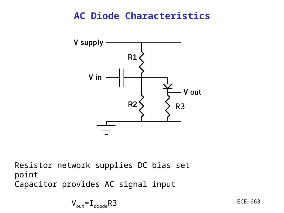
AC Diode Characteristics
Resistor network supplies DC bias set pointCapacitor provides AC signal input
Vout=IdiodeR3
R3

ECE 663
AC small signal resistance

ECE 663
Small signal AC conductance
)()(
11 /
dcdc
kTqVs
VIkTq
VIkTq
g
eAJdVd
dVdI
Rg
Small Signal AC resistance
)(11VIq
kTg
Rdc
Resistance depends on DC set point – voltage controlled resistor

ECE 663
Cdrd
Y1
Zgd i Cd 1
rdi Cd rd, Cd vary with VDC !!!
Reactance:
An equivalent circuit
Let us work out Y for reverse bias first
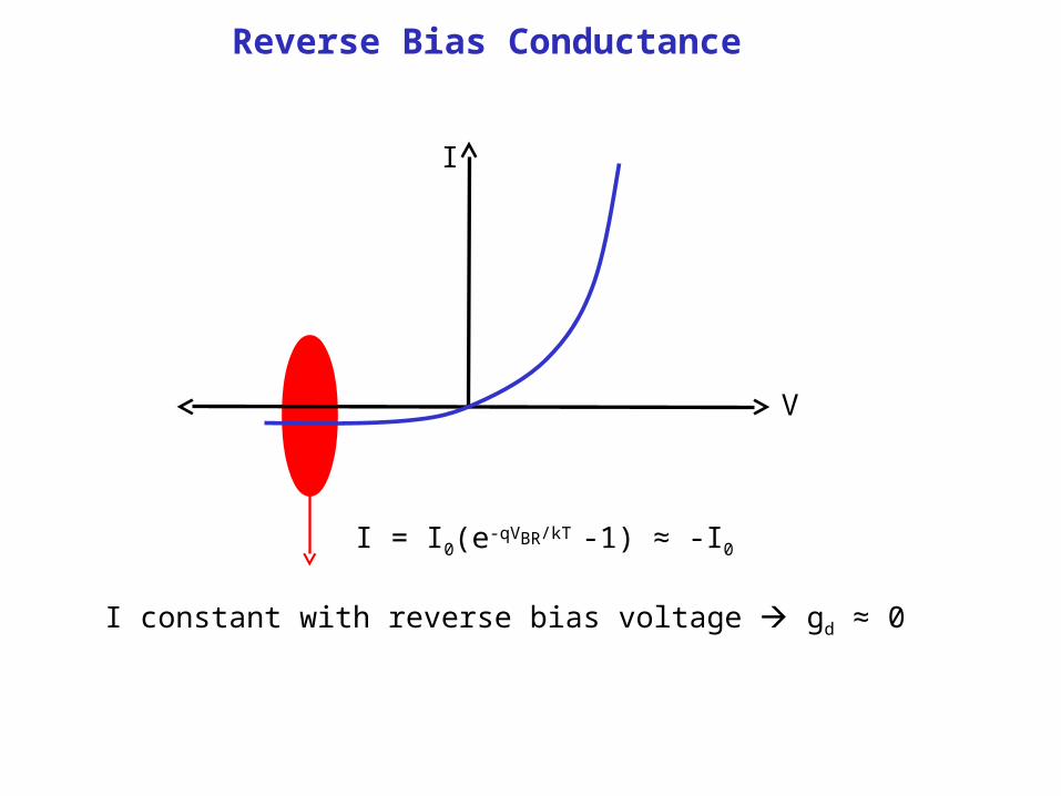
Reverse Bias Conductance
I
V
I constant with reverse bias voltage gd ≈ 0
I = I0(e-qVBR/kT -1) ≈ -I0

ECE 663
Reverse Bias (‘Depletion’) Capacitance
• AC voltage modifies depletion width• Depletion width changes small• Looks like adding charges to parallel
plates• AC capacitance
WAK
C sJ
0

ECE 663
RB capacitance C-V measurements
• Plot of 1/C2 vs V is a straight line (constant doping) and the slope gives doping profile.
• Y-intercept gives built-in voltage
02
2/1
0
2/1
0
0
21
2
2
sB
Abi
J
Abi
sBJ
AbiB
s
sJ
KqNVV
C
VVKqN
C
VVqNK
W
WAK
C

ECE 663

ECE 663
So reverse bias equivalent circuit
WAK
C sJ
0
Rs
Notice that for reverse bias, circuit parameters are frequencyindependent, as if we’re in DC characteristics.
Why?
ECE 663
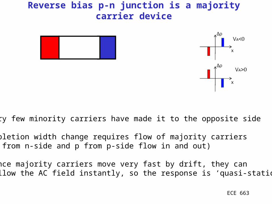
Reverse bias p-n junction is a majority carrier device
Very few minority carriers have made it to the opposite side
Depletion width change requires flow of majority carriers(n from n-side and p from p-side flow in and out)
Since majority carriers move very fast by drift, they can follow the AC field instantly, so the response is ‘quasi-static’

ECE 663
Just how fast are majority carriers?
Drifting charges, with fields in turn determined by charge
∂n/∂t = -(1/q)∂Jn/∂x + (gN - rN)
Jn = qnnE + qDN∂n/∂x ≈ qnnE ≈ nE
Ks0 ∂E/∂x = q(p - n + ND+ - NA
-) ≈ -qn
∂n/∂t = -n/
= Ks/n(Dielectric Relaxation Time)
ECE 663
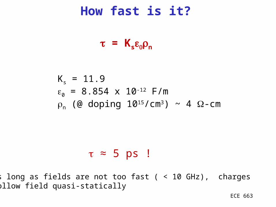
How fast is it?
= Ksn
Ks = 11.90 = 8.854 x 10⁻¹² F/mn (@ doping 1015/cm3) ~ 4 -cm
≈ 5 ps !
As long as fields are not too fast ( < 10 GHz), chargesfollow field quasi-statically

ECE 663
Let’s now go to forward bias
ECE 663
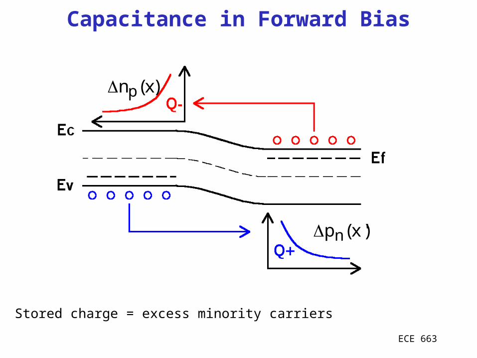
Capacitance in Forward Bias
np x( )
pn x'( )
Stored charge = excess minority carriers

ECE 663
AC field varies minority carrier pile-up (recall law of the
junction)
p(xn) = (ni2/ND)[eq(V + vac)/kT – 1]
ECE 663
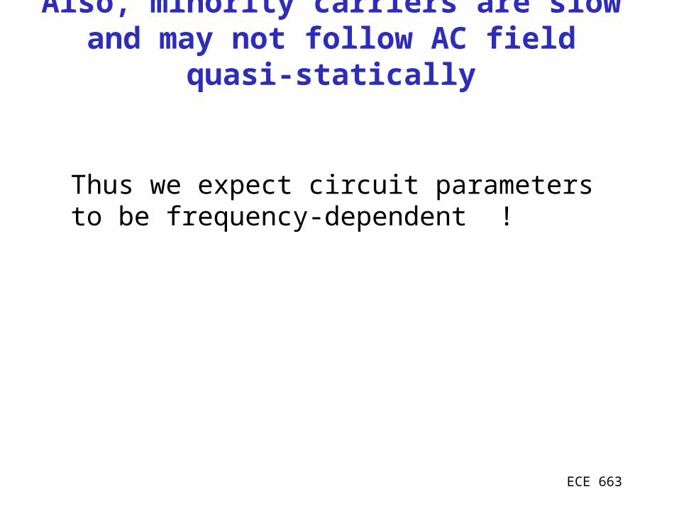
Also, minority carriers are slow and may not follow AC field quasi-
statically
Thus we expect circuit parametersto be frequency-dependent !

ECE 663
How fast are minority carriers?
≈ 1/NTTvt (Minority carrier lifetime)
NT ~ 1012/cm3 (for NA ~ 1014/cm3)T ~ (10-10m)3
vt = 3kT/m ~ 105m/s
≈ 300 s
So for fast fields ( >> 1/), expect carriers to go out of phase, leading tofreq-dependent circuit parameters

ECE 663
But how do we include such phase lag effects?

Back to MCDE
∂n/∂t = DN∂2n/∂x2 – n/n
Can’t drop this at AC fields !!
jn

Back to MCDE
0 = DN∂2n/∂x2 – n(1+jn)/n
n n/(1+jn)

So in Shockley equation
I = qA(ni2/ND)DN (1+jn)
/n
x [eq(V + vac)/kT – 1] idiff = G0(1+jn)vac
idiff = (Gd + jCd)vac

Square root of (1+jn)
1 + j = Aej
A = (1 + 22) = tan-1()
Real(1+j) = A1/2cos(/2)
Im(1+j) = A1/2sin(/2)
cos = 1/(1+22) = 2cos2(/2) - 1 = 1 – 2sin2(/2)
Re(1+j) = Gd
Im(1+j) = jCd
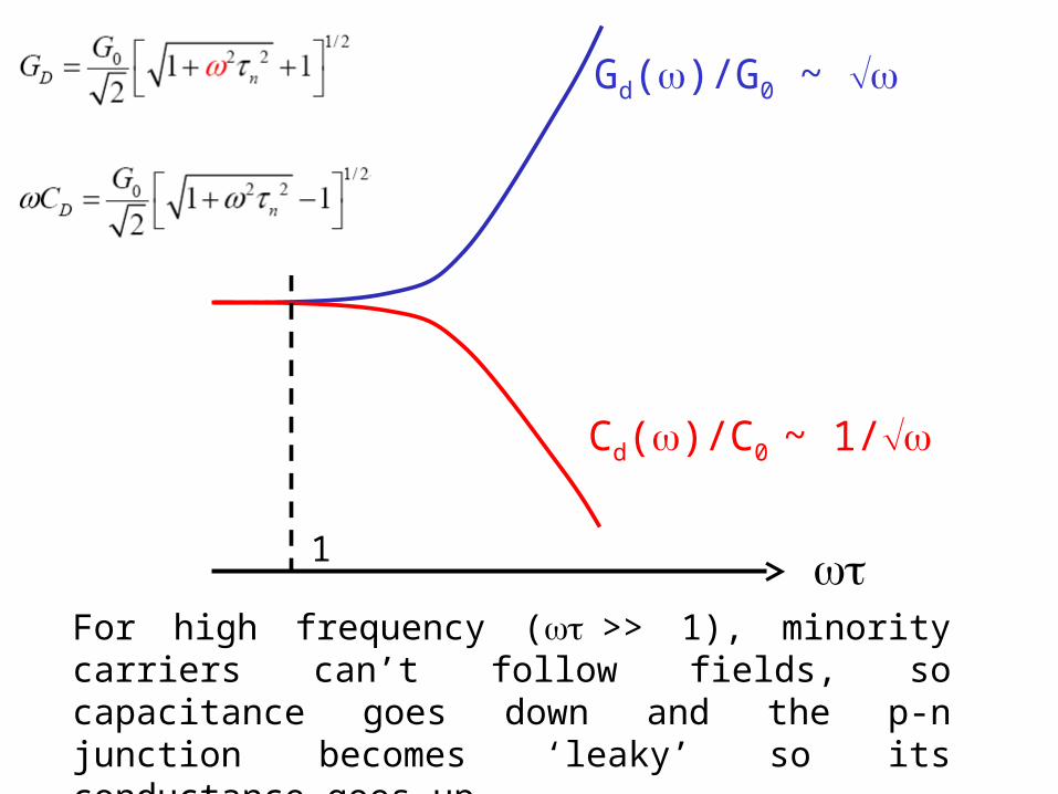
1
Gd()/G0 ~
Cd()/C0 ~ 1/
For high frequency (>> 1), minority carriers can’t follow fields, so capacitance goes down and the p-n junction becomes ‘leaky’ so its conductance goes up
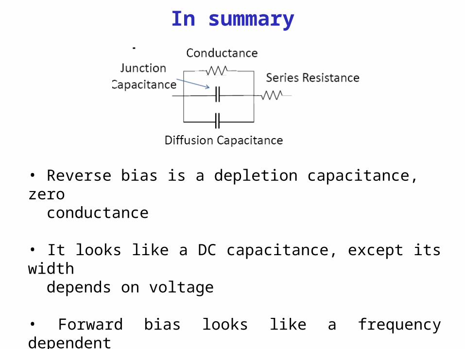
In summary
• Reverse bias is a depletion capacitance, zero conductance
• It looks like a DC capacitance, except its width depends on voltage
• Forward bias looks like a frequency dependent diffusion capacitance and a diffusion conductance to give an overall admittance