ece 1201 semiconductors and diodes
TRANSCRIPT

Solid State Electronics Supplement Semiconductors
Semiconductors are materials having electrical conductivities between conductors and insulators. They have a more limited availability of free electrons – valence electrons that are free to move within the material – than do pure conductors. Semiconductors are useful because the supply of free electrons can be controlled by any or a combination of several means, including chemical (during initial fabrication) and electrical (while the device is a part of a circuit).
An electrical component using semiconductor material consists of a pure base material, usually silicon (Si) or germanium (Ge) in a covalent-bonded crystal, having regions doped with a small concentration of impurities. Silicon and germanium are metalloids each having four valence electrons that provide a small but significant supply of free electrons when at room temperature. By doping the pure material with a small amount (a few parts per billion) of valence-5 material, a much larger supply of conduction electrons is provided and increased conductivity results. A region of semiconductor material doped in this way is called n-type because it has an excess supply of (negative) electrons.
Conversely, doping the base with a valence-3 material places chemical impurities with only three valence electrons in crystal lattice sites normally occupied by a silicon atom. These valence-3 impurities lack one electron needed to form covalent bonds with all four of its silicon neighbors. The resulting 'hole' in the bonding system is easily filled by an electron shifting from an adjacent site (due to normal thermal agitation). Thus the hole is mobile and carries an effective charge of +1 because one proton in the silicon nucleus is not offset by a bonded electron. A region of semiconductor material doped in this way is called p-type because it has an excess supply of positive holes. The P-N Junction
A p-n junction is formed when a piece of p-type and a piece of n-type material meet within a continuous crystal lattice. Electrons from the n-type material are attracted to the positive p-type material and migrate into the p-type material where they drop into holes near the junction completing the available covalent bonds. Near the junction, the p-region has gained electrons and taken on a negative charge, while the n-region has lost electrons and taken on a positive charge. The carrier-free region or depletion region is thus formed. The charge imbalance along the depletion region results in a space charge that establishes an electric potential of a few tenths of a volt across the junction. This electric potential opposes further migration of electrons from n- to p-type material and the depletion zone is maintained essentially free of carriers by this potential.

Figure 1 – The P-N Junction
If an external voltage is applied to the p-n junction that reinforces the space charge potential, the depletion region remains free of carriers and acts as an insulator. No current flows across the junction, the width of the depletion region increases because electrons in the n-type material are attracted to the positive terminal, and holes in the p-type material are attracted to the negative terminal. This condition is called reverse biasing.
When an externally applied potential opposes the space charge potential, the junction remains non-conducting until the external voltage is just large enough to offset the space charge potential. At that point, electrons and holes have sufficient energy to cross the depletion region and a current flows. This condition is called forward biasing.
Figure 2 – Biasing the P-N Junction
A simple p-n junction thus acts as a one-way device, allowing current flow in the forward direction and no current flow in the reverse direction. A device that uses the simple p-n junction in this way is called a diode. Diodes
An ideal diode acts like a short circuit when forward biased and acts like an open circuit when it is reverse biased. In other words, when an ideal diode is conducting, there is no resistance across the p-n junction and no voltage drop across the diode. When an ideal diode is non-conducting, or reverse biased, no current flows through the diode. In simplest terms, diodes allow current flow

in one direction but prevent it in the other. The arrowhead, known as the anode, points in the direction of current flow when the diode is conducting. The other terminal is called the cathode.
Figure 3 – Symbol and V-I Characteristic of an Ideal Diode
Diodes are common semiconductor devices. They are used in power supplies to convert an AC voltage into varying DC voltage (like the half-wave rectifier in Fig. 4), in logic circuits to form gates, and in a variety of other applications. We will discuss the half-wave rectifier below. Half-Wave Rectifier
Figure 4 depicts the half-wave rectifier circuit – a simple circuit demonstrating the ideal diode acting as a switch – and the waveform that results when an AC signal is applied. The circuit consists of an AC voltage source in series connection with a diode (D1) and a resistor (R1). The signal from the AC source is the sine wave Vin shown in the middle of Figure 4 – much like the 120 VAC waveform available at the wall socket.
Figure 4 – The Half-Wave Rectifier and Resulting Waveform

As the voltage rises in the first half-wave, the anode-to-cathode voltage on
D1 positive, and the diode is forward biased (ON). The diode passes current to the load resistor, and the voltage across R1 (Vout) is therefore the same as the source voltage (Vin) during the first and subsequent positive half-waves.
When the source voltage Vin goes negative, the anode-to-cathode voltage is negative, and D1 is now reverse biased (OFF). The diode no longer passes current to the load resistor, and the voltage across R1 (Vout) is zero regardless of the magnitude of Vin. As long as Vin is negative, the diode does not conduct, and Vout remains at zero. As, soon as Vin is positive again, the cycle repeats, D1 turns ON and Vout mirrors Vin. Transistors
The bipolar junction transistor (BJT or “transistor” for short) is a three terminal device consisting of two n-type materials separated by a p-type material (NPN transistor), or two p-type materials separated by an n-type material (PNP transistor). Other types of transistors exist, but this discussion is limited to the BJT for simplicity.
The three sections of the BJT are the emitter, base, and collector. The principles of operation for both types of BJTs are the same with the only difference being the direction of current flow. For this reason, the operation of an NPN transistor is described here, and the principle will be extended to the PNP transistor in a last paragraph.
Figure 5 – Symbols and Conceptualization of the PNP and NPN Transistor
An NPN transistor is operated with the collector positive with respect to
the emitter. If the base is held at the same potential as the emitter, the base-emitter p-n junction is reverse-biased and no current flows through the collector. If the base is biased a few tenths of a volt positive with respect to the emitter, the emitter-base p-n junction becomes forward-biased and a current flows through that junction. This current consists of holes flowing from p- to n-type material and also of electrons flowing from n- to p-type material. The holes that cross into the

n-type collector quickly combine with electrons. The electrons entering the p-type base, however, have a high probability of continuing through to the collector before they recombine with electrons because the base is thin and lightly doped (only a slight excess of holes).
In a properly built transistor, only a small fraction of the electrons entering the base recombine or are picked up by the base lead. Most of them (sometimes over 99 percent) continue through to the collector. Or, in hole-flow terms, an NPN transistor has a collector-to-emitter current many times larger than the base-to-emitter current, and applying a small positive voltage between the base and emitter “turns-on” this current. The base draws a small current (about 1/100th) in comparison to the collector-to-emitter current it controls
In simplest terms, the transistor can be thought of as a switch. A small current applied to the base (the result of a small base-to-emitter voltage) controls current flow from collector-to-emitter. When the base-to-emitter voltage is above some threshold voltage (about +0.5 V), collector-to-emitter current will flow, and the switch is ON. When the base-to-emitter voltage is reduced, collector-to-emitter current goes to zero, and the switch is OFF.
Finally, a PNP transistor operates in much the same manner as an NPN transistor. The chief differences are that the collector is negative with respect to the emitter, the large current flows from emitter-to-collector, and the small control current flows from emitter-to-base. All other aspects of its operation are the same – it is a current controlled switch.

University of Geneva
Diodes
Contents
1 Introduction 11.1 Diode equation . . . . . . . . . . . . . . . . . . . . . . . . . . . . . . . . . . . 2
1.1.1 Reverse Bias . . . . . . . . . . . . . . . . . . . . . . . . . . . . . . . . 21.1.2 Forward Bias . . . . . . . . . . . . . . . . . . . . . . . . . . . . . . . . 2
1.2 General Diode Specifications . . . . . . . . . . . . . . . . . . . . . . . . . . . 3
2 Types of diodes 32.1 Rectifier diodes . . . . . . . . . . . . . . . . . . . . . . . . . . . . . . . . . . . 4
2.1.1 Half-wave rectifier . . . . . . . . . . . . . . . . . . . . . . . . . . . . . 42.1.2 Full-wave rectifier . . . . . . . . . . . . . . . . . . . . . . . . . . . . . . 42.1.3 Rectifier filters . . . . . . . . . . . . . . . . . . . . . . . . . . . . . . . 52.1.4 An application of rectifiers . . . . . . . . . . . . . . . . . . . . . . . . . 5
2.2 Switching diodes . . . . . . . . . . . . . . . . . . . . . . . . . . . . . . . . . . 72.2.1 Clipping . . . . . . . . . . . . . . . . . . . . . . . . . . . . . . . . . . . 72.2.2 Clamping . . . . . . . . . . . . . . . . . . . . . . . . . . . . . . . . . . 7
2.3 Zener diodes . . . . . . . . . . . . . . . . . . . . . . . . . . . . . . . . . . . . 82.4 Optical diodes . . . . . . . . . . . . . . . . . . . . . . . . . . . . . . . . . . . 8
2.4.1 LED (Light Emitting Diode) . . . . . . . . . . . . . . . . . . . . . . . . 82.4.2 Photodiode . . . . . . . . . . . . . . . . . . . . . . . . . . . . . . . . . 82.4.3 Optocoupler . . . . . . . . . . . . . . . . . . . . . . . . . . . . . . . . . 9
1 Introduction
A diode is a dispositive made of a semiconductor material, which has two terminals or elec-trodes (di-ode), that act like an on-off switch. When the diode is “on”, it acts as a short circuitand passes all current. When it is “off”, it behaves like an open circuit and passes no current.The two terminals are different and are marked as plus and minus in figure 1. If the polarityof the applied voltage matches that of the diode (forward bias), then the diode turns “on”.When the applied voltage polarity is opposite (reverse bias), it turns “off”. Of course this isthe theoretical behaviour of an ideal diode, but it can be seen as a good approximation for areal diode.
A diode is simply a pn junction (see ’Introduction into Semiconductor Physics’) with thefollowing characteristics:
• Under forward bias, it needs a small voltage to conduct. This voltage drop is maintainedduring conduction.
• The maximum forward current is limited by heat-dissipation ability of the diode. Usuallyit is around 1000 mA.
• There is a small reverse current.

University of Geneva TPA-Electronique
i
v
i
v
+
−
(c)(b)(a)
Figure 1: (a) Diode symbol. (b) Current-voltage characteristics of an ideal diode. (c) IVcurve for a real diode.
• Every diode has a maximum reverse voltage (breakdown voltage) that cannot be ex-ceeded without diode damage.
n p
Figure 2: A p− n diode junction structure and the equivalent device schematics.
1.1 Diode equation
1.1.1 Reverse Bias
When the diode is reverse-biased, a very small drift current due to thermal excitation flowsacross the junction. This current (reverse saturation current, I0) is given, according to theBoltzmann equation, by the formula:
I0 = K0 e−eV0kT
where K0 is a constant depending on the pn junction geometry and V0 is the built-in voltageof the diode (see chapter “Semiconductor Materials: pn junction”).
1.1.2 Forward Bias
When the diode is forward-biased through a voltage V , a small drift current flows againacross the junction. In that case, however, there is an additional component, the diffusioncurrent Vd, given by the formula:
Id = K0 ee(V−V0)
kT

University of Geneva TPA-Electronique
These two currents have opposite directions, the total current is therefore given by:
I = Id − I0 = K0 e−eV0kT (e
eVkT − 1) = I0(e
eVkT − 1)
1.2 General Diode Specifications
There are four diode ratings that apply in one way or another to all types of diodes andapplications:
1. Forward voltage drop VF : is the forward-conducting junction level (∼0.7 V for Si diodesand 0.3 V for Ge diodes)1.
2. Average forward current IF : is the maximum amount of forward current that the diodecan carry for an indefinite period. If the average current exceeds this value, the diodewill overheat and, eventually, will be destroyed.
3. Peak reverse voltage VR, or reverse breakdown voltage. This is the largest amount ofreverse-bias voltage the diodes’s junction can withstand for an indefinite period of time.If a reverse voltage exceeds this level, the voltage will punch through the depletion layerand allow current to flow backwards through the diode, which is a destructive operation(except for the case of a Zener diode).
4. Maximum power dissipation P . The actual diode power dissipation is calculated mul-tiplying the forward voltage drop and the forward current. Exceeding the maximumpower dissipation will result in thermal breakdown of the diode.
Excessive forward current and reverse breakdown voltage are the most common causesof diode failure. In both cases the diode gets very hot, what destroys the pn junction. Oc-casional peaks of voltage or current exceeding these rates for very short times (few mil-liseconds) may not overheat the junction, but repeated peaks may fatigue the junction. Bydesign, diodes are selected with ratings that exceed two or three times the expected peaksin the circuit.
2 Types of diodes
We can distinguish the following types of diodes:
• Rectifier diodes are typically used for power supply applications. Within the powersupply, you will see diodes as elements that convert AC power to DC power;
• Switching diodes have lower power ratings than rectifier diodes, but can function betterin high frequency application and in clipping and clamping operations that deal withshort-duration pulse waveforms;
1This is the case in the so-called “constant-voltage-drop” or “0.7-V” model. In that model, the current isa step function of the voltage: if the forward voltage is less than 0.7 V, the current which flows through thejunction is zero, if the forward voltage is greater than 0.7, then the voltage drop in the diode is always 0.7 V (inthe case of silicon)

University of Geneva TPA-Electronique
• Zener diodes, a special kind of diode that can recover from breakdown caused whenthe reverse-bias voltage exceeds the diode breakdown voltage. These diodes arecommonly used as voltage-level regulators and protectors against high voltage surges;
• Optical diodes;
• Special diodes, such as varactors (diodes with variable capacity), tunnel diodes orSchottky diodes.
2.1 Rectifier diodes
A rectifier is a dispositive that ideally transforms the AC input voltage into a DC voltage(voltage is always positive or zero). These diodes have the largest ratings and sometimecan be quite big in volume. As a rule of thumb, the bigger the diode (more pn surfacejunction available for heat dissipation), the higher the ratings.
2.1.1 Half-wave rectifier
A half-wave rectifier is composed of a single diode that connects an AC source to a load. Infigure 3 the load is represented by a resistor. The diode conducts on AC voltage only whenits anode is positive with respect to the cathode (i.e. greater than 0.7 V for a silicon diode).The output has therefore only a positive component with an average value:
Vave =1
T
∫ T/2
0
Vp sin wt dt =Vp
π
The output peak voltage is the AC source minus the voltage drop of the diode, that in mostcases can be neglected.
Vin Vout
Vout
Vin
R
V
t
Figure 3: Half wave rectifier. Note the effect of the 0.7 V diode voltage drop. If Vp 0.7V , itcan be neglected.
2.1.2 Full-wave rectifier
In half-wave rectifiers, half of the power provided by the source is not used. To solve thisproblem, we have to use full-wave rectifiers. The minimum full-wave rectifier is composedof two diodes, but it requires a center tapped transformer. Figure 4 shows a bridge rectifier,composed of four diodes, that can use a “normal” transformer.

University of Geneva TPA-Electronique
The AC current, according to its direction, flows either in the top or in the bottom partof the bridge in each half-cycle. In the output voltage we will have a component for bothnegative and positive parts of the input voltage. In both cases the current passes throughtwo forward-biased diodes in series, what produces a voltage drop of 1.4 V.
The average voltage of a full-wave rectifier is:
Vave =1
T/2
∫ T/2
0
Vp sin wt dt =2Vp
π
Vout
Vin
Vin
Vout
V
t
R
Figure 4: Full wave rectifier. In this case the voltage drop, not shown in the graphic, will be1.4 V because two diodes are crossed..
2.1.3 Rectifier filters
The waveforms generated directly by the rectifiers described above, are not very useful, butcan be smoothed to produce almost perfect DC. For that purpose we can use the inertiaproperties of capacitors and inductors.
Although the capacitor does a good job producing DC, a significant ripple voltage re-mains. During the discharging period, the capacitor voltage reduces exponentially. At theend of the discharge, the output voltage is:
Vout = Vpe−(t2−t1)/RLC
The discharging time is t2 − t1 ∼ T , so the ripple voltage is:
vr = ∆V = Vp − Vpe−T/RLC ' Vp
T
RLC=
Vp
νRLC
In case of a full-wave rectifier the ripple voltage is:
vr = VpT
2RLC=
Vp
2νRLC
2.1.4 An application of rectifiers
A significant problem for electrostatic accelerators is the production of sufficiently high ac-celerating voltages. At the beginning of the 1930s, Cockroft and Walton2 developed a high
2J.D. Cockroft, E.T.S. Walton, Proc. Roy. Soc., A136, 619 (1932), A137, 229 (1932), A144, 704 (1934)
University of Geneva TPA-Electronique
Vin
Vin VoutRL
Rd
Vin VoutRLC
Vin VoutRL
VoutV
t
C C
(b)
(c)
(a)
(d)
charge
discharge
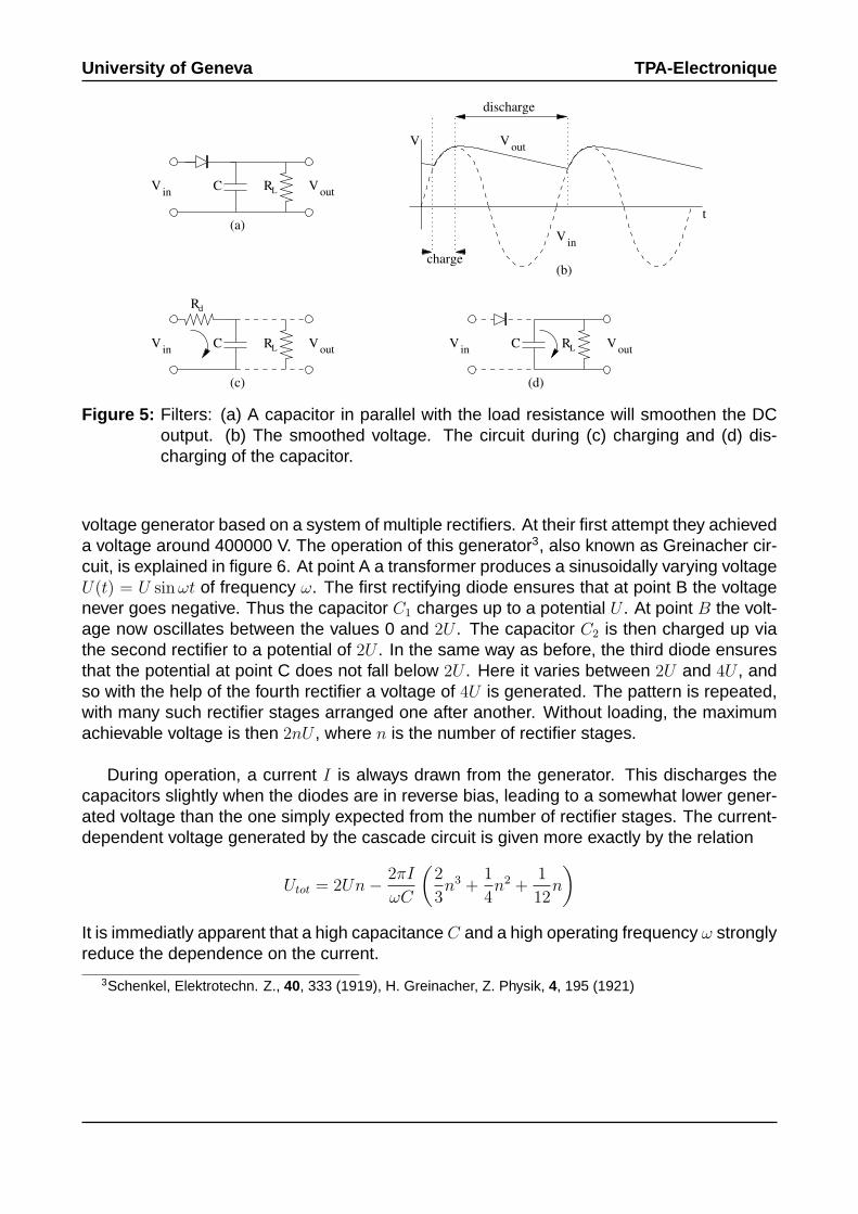
Figure 5: Filters: (a) A capacitor in parallel with the load resistance will smoothen the DCoutput. (b) The smoothed voltage. The circuit during (c) charging and (d) dis-charging of the capacitor.
voltage generator based on a system of multiple rectifiers. At their first attempt they achieveda voltage around 400000 V. The operation of this generator3, also known as Greinacher cir-cuit, is explained in figure 6. At point A a transformer produces a sinusoidally varying voltageU(t) = U sin ωt of frequency ω. The first rectifying diode ensures that at point B the voltagenever goes negative. Thus the capacitor C1 charges up to a potential U . At point B the volt-age now oscillates between the values 0 and 2U . The capacitor C2 is then charged up viathe second rectifier to a potential of 2U . In the same way as before, the third diode ensuresthat the potential at point C does not fall below 2U . Here it varies between 2U and 4U , andso with the help of the fourth rectifier a voltage of 4U is generated. The pattern is repeated,with many such rectifier stages arranged one after another. Without loading, the maximumachievable voltage is then 2nU , where n is the number of rectifier stages.
During operation, a current I is always drawn from the generator. This discharges thecapacitors slightly when the diodes are in reverse bias, leading to a somewhat lower gener-ated voltage than the one simply expected from the number of rectifier stages. The current-dependent voltage generated by the cascade circuit is given more exactly by the relation
Utot = 2Un− 2πI
ωC
(2
3n3 +
1
4n2 +
1
12n
)It is immediatly apparent that a high capacitance C and a high operating frequency ω stronglyreduce the dependence on the current.
3Schenkel, Elektrotechn. Z., 40, 333 (1919), H. Greinacher, Z. Physik, 4, 195 (1921)

University of Geneva TPA-Electronique
C1
C3
C5
C6
C4
C2B
C
D
A
A
B
C
D
2U
6U
4U
U
voltage
time
2U
4U
6U
U
0
Figure 6: Schematic drawing explaining the operation of the Cockroft-Walton cascade gen-erator.
2.2 Switching diodes
2.2.1 Clipping
The function of a clipping circuit is to cut off part of an input waveform.
Vin V1 V2
Vout
V1
V2
Vout
Vin
V
t
R
−
+ −
+
Figure 7: Clipping principle.
2.2.2 Clamping
If the DC value of a signal needs to be changed, a capacitor can be charged with the ap-propriate value. When connected in series with the signal source, it will then provide thedesired DC level.
Vp V − Vp V + Vp
0 0
(a) (b) (c)
0
+ −
VV0
+ − + −
00
V
−V+ +
Figure 8: Clamping principle.

University of Geneva TPA-Electronique
For positive values of the input signal, the diode immediately conducts, allowing the ca-pacitor to be charged. The RC time constant is small because the only resistor presentis the small internal resistor of the diode (less than 1 Ω). For negative values of the inputsignal, the diode is reverse-biased, so the capacitor cannot be discharged, maintaining thepotential. In general, if we use a battery of voltage V , the output signal will be:
Vout = −Vp + V + Vp sin wt = Vp(sin wt− 1) + V
2.3 Zener diodes
A conventional solid-state diode will not let current flow up to its breakdown voltage if reverse-biased. By exceeding the breakdown voltage, a conventional diode is destroyed duringbreakdown due to excess current and overheating. In case of forward-bias (in the directionof the arrow), the diode exhibits a voltage drop of roughly 0.7 V. The voltage drop dependson the type of the diode.
A Zener diode exhibits almost the same properties, except the device is especially de-signed so as to have a greatly reduced breakdown voltage, the so-called Zener voltage. AZener diode contains a heavily doped pn junction allowing electrons to tunnel from the va-lence band of the p-type material to the conduction band of the n-type material. A reverse-biased Zener diode will exhibit a controlled breakdown and let the current flow to keep thevoltage across the Zener diode at the Zener voltage. For example, a 3.2 V Zener diode willexhibit a voltage drop of 3.2 V if reverse biased. However, the current is not unlimited, sothe Zener diode is typically used to generate a reference voltage for an amplifier stage. Thebreakdown voltage can be controlled quite accurately in the doping process. Tolerances upto 0.05% are achievable, though the most widely used tolerances are 5% and 10%. The ef-fect was discovered by the American physicist Clarence Melvin Zener. In figure 9, the Zenerbehaviour is illustrated:
2.4 Optical diodes
2.4.1 LED (Light Emitting Diode)
A light-emitting diode (LED) is a semiconductor device that emits incoherent monochromaticlight when electrically biased in the forward direction. The colour depends on the semicon-ducting material used, and can be near-ultraviolet, visible or infrared. The wavelength ofthe light emitted, and therefore its colour, depends on the bandgap energy of the materialsforming the pn junction. A normal diode, typically made of silicon or germanium, emits invis-ible far-infrared light. Currently used materials for LEDs are gallium arsenide (GaAs) for theinfrared, gallium arsenide phospate (GaAsP) for yellow and red light, and gallium phosphate(GaP) for red and green light. The intensity of the light depends on the current that passesthrough the LED.
2.4.2 Photodiode
A photodiode is a diode working in reverse polarization and having a window where the lightcan enter and hit directly the pn junction. As in the case of the LED, the energy level of theimpurities has been chosen in order to allow electrons to jump from valence to conduction

University of Geneva TPA-Electronique
zI
zV
Vi
Vz
V
V
V
max
min
t
I
I
max
min
(a)
(b) (c)
R
RV Vin out
s
L
I
Vz
Figure 9: (a) A voltage regulator is inserted between the input voltage and the load. (b) TheZener current Iz varies between Imax and Imin in response to the varying inputvoltage so as to keep the load current and the load voltage constant (c).
band. In the absence of light the leakage current is negligible, but when light is present, theleakage current increases to measurable values.
2.4.3 Optocoupler
An optopcoupler is a device that combines a LED and a photodiode in such a way thatthe light emitted by the LED hits the photodiode. LED and photodiode can be connectedto different circuits, so this device allows to send a signal between two isolated networkscoupled just through light emission and reception.
References
[1] The Physics of Information Technology, Neil Gershenfeld, Cambridge University Press(2000)
[2] Electronics and Communications for Scientist and Engineers, Martin Plonus, HarcourtAcademic Press (2001)
[3] Introduction to Electrodynamics, 3rd edition, David J. Griffiths, Prentice Hall (1999)

University of Geneva TPA-Electronique
[4] The Art of Electronics, 2nd edition, P. Horowitz, W. Hill, Cambridge University Press(1989)
[5] Engineer Mathematics, A. Croft, R. Davison, M. Hargreaves, Prentice Hall (2001)
[6] The Physics of Particle Accelerators, K. Wille, Oxford Univ. Press)
[7] Foundations of Electronic Circuits and Devices, R.L. Meade, R. Diffenderfer, Ed. Thom-son Delmar Learning
[8] http://en.wikipedia.org

Sheet 1 Semiconductor Diodes
Dio
des
DIODE1
The Semiconductor Diode
The semiconductor diode is a device that will conduct current in one direction only. It is the electrical equivalent of a hydraulic check valve. The semiconductor diode has the following characteristics: • A diode is a two-layer semiconductor consisting of an Anode comprised of P-Type semiconductor material
and a Cathode which is made of N-Type semiconductor material. • The P-Type material contains charge carriers which are of a positive polarity and are known as holes. In the
N-Type material the charge carriers are electrons which are negative in polarity. • When a semiconductor diode is manufactured, the P-Type and N-Type materials are adjacent to one another
creating a P-N Junction.
Biasing
A bias refers to the application of an external voltage to a semiconductor. There are two ways a P-N junction can be biased. • A forward bias results in current flow through the diode (diode conducts). To forward bias a diode, a positive
voltage is applied to the Anode lead ( which connects to P-Type material) and the negative voltage is applied to the Cathode lead ( which connects to N-Type material).
• A reverse bias results in no current flow through the diode (diode blocks). A diode is reverse biased when the
Anode lead is made negative and the Cathode lead is made positive.
P-N Junction Characteristics
The P-N Junction region has three important characteristics:
1) The junction is region itself has no charge carriers and is known as a depletion region. 2) The junction (depletion) region has a physical thickness that varies with the applied voltage. A forward
bias decreases the thickness of the depletion region; a reverse bias increases the thickness of the depletion region.
3) There is a voltage, or potential hill, associated with the junction. Approximately 0.3 of a volt is required to
forward bias a germanium diode; 0.5 to 0.7 of a volt is required to forward bias a silicon diode.
-V +V
Diode X-Y Characteristic Curve
+I
-I
PIV
VF
- +
Current Flow
+ -
P N
Forward Bias
P N
Reverse Bias (No Current Flow)
Symbol
Anode Cathode
Axial Lead Diode
A C (K)

Sheet 2 Silicon Diodes
Dio
des
DIODE2
Ratings
Three characteristics must be defined for proper application or replacement of a semiconductor diode: Voltage Rating is the maximum voltage which the diode will block in the reverse-biased mode. • This is expressed as the Peak-Reverse-Voltage (PRV) or Peak-Inverse-Voltage (PIV). • It is important to remember that this is a peak value of voltage not the root-mean-square (RMS) value. As a
“Rule -of-Thumb, to provide a margin of safety, the PIV rating of a diode should be at least 3 times the RMS voltage of the circuit.
Current Rating is the maximum current the device can carry in the forward biased direction. Package Configuration • Small, low current diodes are available in an axial lead configuration. The band end is the cathode. • High current diodes come in a press-fit, stud- mounted, or hockey puck package.
Stud mounted diodes are available in Standard Polarity (stud cathode) and Reverse Polarity (stud anode).
Thermal Limits
• It is essential that semiconductors operate within the device temperature ratings. • Semiconductor charge carriers are released thermally as well as electrically. Heat-sinking may be required
during soldering and when the device is in operation to prevent thermal damage. • The forward resistance of a diode decreases with temperature; this results in an increase in current, which in
turn produces more heat. As a result, thermal run-away can occur and destroy the semiconductor.

Sheet 3 Diode Test Procedure D
iod
es DIODE3
Forward Bias - Diode Conducts. Correct reading: Meter will read about 0.5 - 0.8 volt.
Unlike its predecessor, the Analog Ohmmeter, Digital Ohmmeters re-quire a special Diode Check Function because the current circulated by the normal Ohms Function of a digital meter is too low to adequately check a diode. In the Diode Check Position, the reading given by a digital meter in the forward bias direction (meter positive to diode anode and meter negative to diode cathode) is actually the voltage required to overcome the inter-nal diode junction potential. For a silicon diode this will be about 0.5 - 0.8 volt; a germanium diode will read slightly lower, about 0.3 - 0.5 volt. Symbol Notation K (or C) = Cathode, A = Anode.
TPI 183 Digital Multimeter
Reverse Bias - Diode Blocks Correct reading: TPI Meter will read OUCH for open circuit indication. (Some meters read OL.)
K A
K A
Diode Test Procedure Caution: Ohms and Diode Check measurements can be made only on de-energized circuits! The Ohmmeter battery provides power to make this measurement. You may need to remove the diode from the circuit to get a reliable test. See Note below.
• Connect leads to meter as shown - Black COM, Red Ω .
• Select the (Diode Test) function.
• Connect the leads to the Diode-Under-Test as shown in the drawing above and verify the readings are correct for both a forward and reverse bias. (This is sometimes referred to as checking the front-to-back ratio.)
Note: Large Stud-Mounted Diodes are bolted to a heat sink and Hockey Puck Units are compressed between the heat sinks; removing them from the circuit can be time-consuming and may be unnecessary. In these situations, test the entire assembly first, then, if the assembly tests shorted, remove and test the diodes individually. Hockey Puck Diodes must be compressed in a heat sink assembly or test fixture to be tested as they require compression to make-up the internal connections.
Select
Incorrect Readings: If meter reads 0 both directions, it is shorted. If it reads OUCH (open circuit) both directions, it is open.

Sheet 4 Rectifier Circuits
Rectifiers
Rectification • Rectification is the process of converting an Alternating Current (AC) to a Direct Current (DC). • In the circuits below, the DC output voltage is defined as pulsating DC because it has the same waveform as
one-half cycle of the applied alternating current. It is DC because it always has the same polarity with respect to zero volts. On single-phase rectifiers, the output DC voltage goes to zero after each rectified half cycle.
• To convert a pulsating DC to a pure DC, such as that produced by a battery or DC generator, the DC output
voltage must be filtered. • The diode symbol points in the direction of conventional current flow (positive to negative). • To analyze the operation of a rectifier circuit supplied by an AC circuit, arbitrarily assign a polarity to the
transformer winding and analyze the diode operation, then reverse the polarity assignment and again analyze the operation of the diode. When the anode of the diode is made positive with respect to the cathode the diode will conduct. When the anode of the diode is made negative with respect to the cathode the diode will block the flow of current.
• When the diode is conducting , current flows through the diode and the voltage drop across the diode is very
small (typically 0.5 - 0.7 volts for a silicon diode). The current flow through the load resistor produces a volt-age drop across the load resistor.
• When the diode is non-conducting, no current flows through the diode and the applied voltage appears across
the diode. Because there is no current flow, there will be no voltage drop across the resistor.
AC Input Voltage DC Output Voltage
0V
0V
0V 0V
0V
DCOUT = VRMS / 2 = 12 VDC
DCOUT = VRMS = 24 VDC
DCOUT = VRMS = 12 VDC
DIODE4
RL
+
Center-Tap Circuit
_ 12VAC
12VAC
120 VAC
RL 24
+ _
Bridge Circuit
120 VAC
RL
+
_
Half-Wave Rectifier
24 VAC 120 VAC
24 VAC RMS
24 VAC RMS
12 VAC RMS
0V

Sheet 5 Three-Phase Rectifiers R
ectifiers DIODE5
Three-Phase Half-Wave Rectifier
On three-phase rectifiers, the pulsations do not return to zero as with a single phase rectifier. This reduces the amount of ripple and simplifies filtering. A diode is forward biased when the anode is made more positive with respect to the cathode. Each of the diodes is forward biased when the voltage of the phase leading it becomes lower than the diode anode voltage and the diode is reverse biased when the voltage of the phase lagging it becomes higher that diode anode voltage.
Output Waveform
+
A
B
C
Delta-Wye Rectifier Transformer
RL
Three-Phase Full-Wave Rectifier
Showing rectifier transformer delta secondary only. When the diodes are replaced with SCR’s, the output voltage of the rectifier can be controlled by phase-firing of the SCR’s. This arrangement is referred to as a six-pulse system.
Six-Phase Systems
Some special medium-voltage rectifier transformers have dual secondary windings - one delta, the other wye - which are 30 degrees out-of-phase. The phase-to-phase voltage of the wye matches the phase voltage of the delta. The outputs are individu-ally rectified and the rectifiers are connected in series, resulting in a six-phase sys-tem with very low ripple, that has an output voltage which is double the voltage of the individual windings. The dashed line in the corner of the delta shows the phase shift between the two windings.
RL
+
Positive Bus
Negative Bus

EECS 42 Spring 2001 Copyright Regents of University of California W. G. Oldham Lecture 24
1
LECTURE 24
DIODES –ELECTRICAL BEHAVIOR
Ntype
Ptype
Schematic Device
+− V
I
ISymbol
+− V
Qualitative I-V characteristics:I
V
V positive, easy conduction
V negative, no conduction
Quantitative I-V characteristics:
)1e(II kTqV0 −=
In which kT/q is 0.026V and IO is a constant depending on diode area. Typical values: 10-12 to 10-
16 A. Interestingly, the graph of this equation looks just like the figure to the left.

EECS 42 Spring 2001 Copyright Regents of University of California W. G. Oldham Lecture 24
2
LECTURE 24
DIODES –ELECTRICAL BEHAVIOR
Ntype
Ptype
Schematic Device
+− V
I
What does the physical device look like? (An example of a cross-section)
VP-Type Si
N-Type Si
+−
I
Oxide Metal

EECS 42 Spring 2001 Copyright Regents of University of California W. G. Oldham Lecture 24
3
THE PN JUNCTION DIODE (cont.)
In EECS 105, 130, and other courses you will learn why the I vs. V relationship for PN junctions is of the form
)1e(II kTqV0 −=
where I0 is a constant proportional to junction area and depending on doping in P and N regions, k is Boltzman constant, and T is absolute temperature.
a typical value for I0 is
,106.1hargec electronicq 19−×==
,Kat300 0.026VqKT °= A1010 1512 −− −
We note that in forward bias, I increases exponentially and is in the µA-mA range for voltages typically in the range of 0.6-0.8V. In reverse bias, the current is essentially zero.
I-V characteristic of PN junctions

EECS 42 Spring 2001 Copyright Regents of University of California W. G. Oldham Lecture 24
4
DIODE I-V CHARACTERISTICS AND MODELS
The equation
is graphed below for
1)kTqVexp(II 0 −=
A10I 150
−=
The characteristic is described as a “rectifier” – that is, a device that permits current to pass in only one direction. (The hydraulic analog is a “check value”.) Hence the symbol:
+− V
I
Simple “Perfect Rectifier” Model
If we can ignore the small forward-bias voltage drop of a diode, a simple effective model is the “perfect rectifier,” whose I-V characteristic is given below:
V
I
Reverse bias0Vany ,0I <≅
Forward bias0Iany ,0V >≅
A perfect rectifier
0
100
200
300
400
-5 -3 -1 1forward bias (V)
Cu
rre
nt
(mic
roa
mp
)

EECS 42 Spring 2001 Copyright Regents of University of California W. G. Oldham Lecture 24
5
DIODE I-V CHARACTERISTICS AND MODELS
Improved “Large-Signal Diode” Model:If we choose not to ignore the small forward-bias voltage drop of a diode, it is a very good approximation to regard the voltage drop in forward bias as a constant, about 0.7V. the “Large signal model” results.
Reverse bias0Vany ,0I <≅
Forward bias0Iany ,0.7V >≅
0
100
200
300
400
-5 -3 -1 1forward bias (V)
Cu
rre
nt
(mic
roa
mp
)
+− V
I
The Large-Signal Diode Model
- 0.7+
V
I
0.7

EECS 42 Spring 2001 Copyright Regents of University of California W. G. Oldham Lecture 24
6
COOL THINGS A DIODE CAN DO(Use perfect rectifier model)
VS(t)
t
+
−
VR(t)+−VS(t)
VR(t)
“rectified” version of input waveform
t

EECS 42 Spring 2001 Copyright Regents of University of California W. G. Oldham Lecture 24
7
MORE THINGS A DIODE CAN DO (PEAK DETECTOR)
+
−
VC(t)Vi(t)+
−
C
Vi(t)
Vi
t
VC(t) VC
+−
EECS 42 Spring 2001 Copyright Regents of University of California W. G. Oldham Lecture 24
8
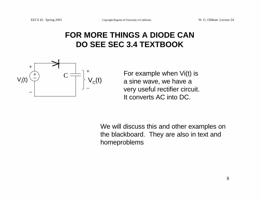
FOR MORE THINGS A DIODE CAN DO SEE SEC 3.4 TEXTBOOK
+
−
VC(t)Vi(t)+
−
C+−
For example when Vi(t) is a sine wave, we have a very useful rectifier circuit. It converts AC into DC.
We will discuss this and other examples on the blackboard. They are also in text and homeproblems

EECS 42 Spring 2001 Copyright Regents of University of California W. G. Oldham Lecture 24
9
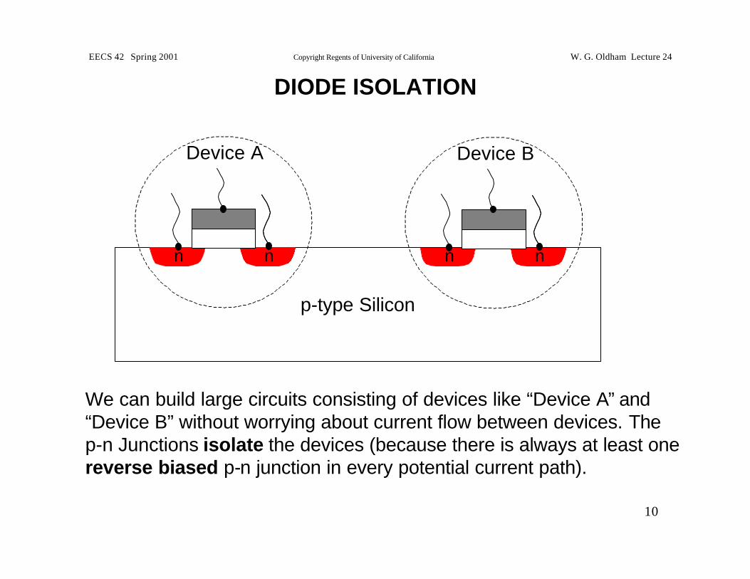
WHY DIODES ARE IMPORTANT IN INTEGRATED CIRCUITS --- ISOLATION
p-type Silicon
n n n n n
regions of n-type Silicon
No current flows if voltages are applied between N-type regions because two P-N junctions are “back to back”
n-regionn-region
p-regionThus, diodes isolate n-regions in p-type substrate and vice versa.
EECS 42 Spring 2001 Copyright Regents of University of California W. G. Oldham Lecture 24
10
DIODE ISOLATION
p-type Silicon
n n
Device A
n n
Device B
We can build large circuits consisting of devices like “Device A” and “Device B” without worrying about current flow between devices. The p-n Junctions isolate the devices (because there is always at least one reverse biased p-n junction in every potential current path).

1N5225 thru 1N5267Vishay Semiconductorsformerly General Semiconductor
Document Number 88305 www.vishay.com18-Apr-02 1
Zener DiodesZener Voltage Range 3.0 to 75V
Power Dissipation 500mW
Features• Silicon Planar Power Zener Diodes.
• Standard Zener voltage tolerance is ±5% with a “B” suffix.Other tolerances are available upon request.
• These diodes are also available in MiniMELF case withthe type designation ZMM5225 ... ZMM5267, SOT-23case with the type designation MMBZ5265 ...MMBZ5267 and SOD-23 case with the typesdesignation MMSZ5225 ... MMSZ5267
Mechanical DataCase: DO-35 Glass Case
Weight: approx. 0.13g
Packaging codes/options:D7/10K per 13” reel, (52mm tape), 20K/boxD8/10K per Ammo tape (52mm tape), 20K/box
DO-204AH(DO-35 Glass)
Dimensions in inches and (millimeters)
Maximum Ratings and Thermal Characteristics (TA = 25°C unless otherwise noted)
Parameter Symbol Value Unit
Zener Current (see Table “Characteristics”)
Power Dissipation at Tamb = 75°C Ptot 500(1) mW
Thermal Resistance Junction to Ambient Air RθJA 300(1) °C/W
Maximum Junction Temperature Tj 175 °C
Storage Temperature Range TS –65 to +175 °C
Note:(1) Valid provided that leads at a distance of 10mm from case are kept at ambient temperature.

1N5225 thru 1N5267Vishay Semiconductorsformerly General Semiconductor
www.vishay.com Document Number 883052 18-Apr-02
Electrical Characteristics (TA = 25°C unless otherwise noted) Maximum VF = 1.1V at IF = 200mA
Maximum ReverseMaximum Zener Impedance(1) Typical Leakage Current
Nominal Zener TemperatureVoltage(3) Test Current at IZK = 0.25mA Coefficient Test Voltage Maximum Regulator
Type at IZT VZ (V) IZT (mA) at IZT ZZT (Ω) ZZK (Ω) α VZ (% / °C) IR (µA) VR (V) Current (2) IZM (mA)
1N5225 3.0 20 29 1600 – 0.075 50 1.0 1521N5226 3.3 20 28 1600 –0.070 25 1.0 1381N5227 3.6 20 24 1700 –0.065 15 1.0 1261N5228 3.9 20 23 1900 –0.060 10 1.0 1151N5229 4.3 20 22 2000 –0.055 5.0 1.0 1061N5230 4.7 20 19 1900 ±0.030 5.0 2.0 971N5231 5.1 20 17 1600 ±0.030 5.0 2.0 891N5232 5.6 20 11 1600 +0.038 5.0 3.0 811N5233 6.0 20 7 1600 +0.038 5.0 3.5 761N5234 6.2 20 7 1000 +0.045 5.0 4.0 731N5235 6.8 20 5 750 +0.050 3.0 5.0 671N5236 7.5 20 6 500 +0.058 3.0 6.0 611N5237 8.2 20 8 500 +0.062 3.0 6.5 551N5238 8.7 20 8 600 +0.065 3.0 6.5 521N5239 9.1 20 10 600 +0.068 3.0 7.0 501N5240 10 20 17 600 +0.075 3.0 8.0 451N5241 11 20 22 600 +0.076 2.0 8.4 411N5242 12 20 30 600 +0.077 1.0 9.1 381N5243 13 9.5 13 600 +0.079 0.5 9.9 351N5244 14 9.0 15 600 +0.082 0.1 10 321N5245 15 8.5 16 600 +0.082 0.1 11 301N5246 16 7.8 17 600 +0.083 0.1 12 281N5247 17 7.4 19 600 +0.084 0.1 13 271N5248 18 7.0 21 600 +0.085 0.1 14 251N5249 19 6.6 23 600 +0.086 0.1 14 241N5250 20 6.2 25 600 +0.086 0.1 15 231N5251 22 5.6 29 600 +0.087 0.1 17 211N5252 24 5.2 33 600 +0.087 0.1 18 19.11N5253 25 5.0 35 600 +0.089 0.1 19 18.21N5254 27 4.6 41 600 +0.090 0.1 21 16.81N5255 28 4.5 44 600 +0.091 0.1 21 16.21N5256 30 4.2 49 600 +0.091 0.1 23 15.11N5257 33 3.8 58 700 +0.092 0.1 25 13.81N5258 36 3.4 70 700 +0.093 0.1 27 12.61N5259 39 3.2 80 800 +0.094 0.1 30 11.61N5260 43 3.0 93 900 +0.095 0.1 33 10.61N5261 47 2.7 105 1000 +0.095 0.1 36 9.71N5262 51 2.5 125 1100 +0.096 0.1 39 8.91N5263 56 2.2 150 1300 +0.096 0.1 43 –1N5264 60 2.1 170 1400 +0.097 0.1 46 –1N5265 62 2.0 185 1400 +0.097 0.1 47 –1N5266 68 1.8 230 1600 +0.097 0.1 52 –1N5267 75 1.7 270 1700 +0.098 0.1 56 –
Notes:(1) The Zener impedance is derived from the 1 kHz AC voltage which results when an AC current having an RMS value equal to 10% of the Zener current (IZT or
IZK) is superimposed on IZT or IZK. Zener impedance is measured at two points to insure a sharp knee on the breakdown curve and to eliminate unstable units(2) Valid provided that leads at a distance of 10 mm from case are kept at ambient temperature(3) Measured with device junction in thermal equilibrium

1N5225 thru 1N5267Vishay Semiconductorsformerly General Semiconductor
Document Number 88305 www.vishay.com18-Apr-02 3
Ratings and Characteristic Curves (TA = 25°C unless otherwise noted)