modeling of iii-nitride quantum wells with arbitrary ...keywords: iii-nitride semiconductors,...
TRANSCRIPT

Modeling of III-Nitride Quantum Wells with Arbitrary Crystallographic
Orientation for Nitride-Based Photonics
Mikhail V. Kisin*, Robert Brown and Hussein S. El-Ghoroury
Ostendo Technologies, Inc. *Corresponding author: 6185 Paseo del Norte, Ste. 200, Carlsbad, CA 92011 ([email protected])
Abstract: A program for self-consistent
modeling of electron-hole energy spectrum and
space-charge distribution in III-nitride based
quantum well (QW) structures has been
developed. The program assumes arbitrary
crystallographic orientation of the
heterostructure template. The model takes into
consideration full 6-band description of the
valence band states, nonparabolicity of the
electron spectrum, quantum confinement of
electrons and holes, strain induced modifications
of the band structure, spontaneous- and piezo-
polarization fields, background layer doping, and
variable level of charge carrier injection.
Calculated optical characteristics include
electron-hole optical susceptibility, spontaneous
and stimulated emission rates, polarization
coefficients for light emission and absorption,
radiative recombination rates, and optical gain
spectra in optically active nitride QWs.
Keywords: III-Nitride semiconductors,
nonpolar and semipolar structures, light emitting
diodes, laser diodes, photonics.
1. Introduction
Applications of nitride-based photonic
devices in visible and UV optical ranges are
growing rapidly. The most commonly used
heterostructures for such applications include a
sequence of GaInN quantum wells grown on a
polar substrate plane (crystallographic hexagonal
c-plane). Even in this symmetric configuration,
the quantum mechanical description of the QW
electronic properties and subsequent modeling of
the QW optical characteristics is very
complicated if compared to more traditional
III-V semiconductor materials with highly
symmetric cubic crystal lattice. III-Nitride
structures grown on nonpolar and semipolar
substrates with less symmetric crystallographic
planes (m-type and a-type planes) are much more
favorable for optoelectronic devices due to the
lower piezo-polarization fields and, possibly,
higher level of indium incorporation in the QW
composite material. Correspondingly, the
modeling complexities grow.
2. The Model
To provide an adequate tool for modeling the
nitride-based devices with nonpolar/semipolar
growth planes the multiband matrix Hamiltonian
established for semiconductors with hexagonal
symmetry has been transformed to an inclined
coordinate system related to the growth plane of
the reduced symmetry. The resulting system of
six equations for valence band states (holes), an
effective-mass Schrodinger equation for
conduction band states (electrons), and Poisson
equation for the confined carriers has been
solved iteratively for an arbitrary level of
injected carrier concentration. The strain tensor
components calculated in the inclined coordinate
system affect the solution and eigenstates both
through the deformation potential terms in the
Hamiltonian and by contributing to the induced
piezo-polarization charges at the QW
boundaries.
3. The Modeling
The general structure of the developed
software is analogous to previously reported
programs for mid-infrared QW lasers based on
cubic semiconductors [1]. Due to inadequate
capabilities of COMSOL GUI for quantum
mechanical calculations, most of the modeling
was performed directly in COMSOL. A one-
dimensional eigenvalue solver for quantum
mechanical equations and a stationary solver for
Poisson equation have been used iteratively
revealing good conversion rate (5-15 iterations
per step-like increase in the injected carrier
concentration). Special subprograms were
developed for orthogonalization of the
degenerate valence band eigenstates, QW
subband dispersion analysis, modeling of the
temperature-induced carrier redistribution
between the QW subbands, and calculation of
the structure optical characteristics.
Program input includes band structure
parameters of binary nitride compounds and
bowing parameters for the interpolation scheme,
elastic, piezoelectric and dielectric constants,
structure layout, electrical bias and ambient
conditions.
The modeling provides the following
information: conduction and valence band
profiles including spontaneous polarization,
piezo-polarization and self-consistent Coulomb
field due to the charge redistribution in QWs,
strain and deformation tensor components,
confined energy levels and subband dispersions,
electron and hole subband density of states
functions, carrier distribution functions and
subband populations at arbitrary level of
injection, matrix elements and anisotropy
coefficients for optical transitions, spontaneous
and stimulated emission spectra, effective
radiative recombination rate, QW optical gain
spectra and carrier-induced refractive index
change, differential and peak optical gain
coefficients, temperature and injection
dependencies of the calculated characteristics.
4. Illustrative results
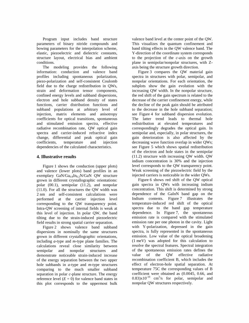
Figure 1 shows the conduction (upper plots)
and valence (lower plots) band profiles in an
exemplary GaN/Ga0.8In0.2N/GaN QW structure
grown in different crystallographic orientations:
polar (00.1), semipolar (11.2), and nonpolar
(11.0). For all the structures the QW width was
2 nm and self-consistent calculations were
performed at the carrier injection level
corresponding to the QW transparency point.
Intra-QW screening of internal fields is weak at
this level of injection. In polar QW, the band
tilting due to the strain-induced piezoelectric
field results in strong spatial carrier separation.
Figure 2 shows valence band subband
dispersions in nominally the same structures
grown in different crystallographic orientations,
including a-type and m-type plane families. The
calculations reveal close similarity between
semipolar and nonpolar structures and
demonstrate noticeable strain-induced increase
of the energy separation between the two upper
hole subbands in a-type and m-type structures
comparing to the much smaller subband
separation in polar c-plane structure. The energy
reference level (E = 0) for valence band states in
this plot corresponds to the uppermost bulk
valence band level at the center point of the QW.
This visualizes the quantum confinement and
band tilting effects in the QW valence band. The
Y-direction of the coordinate system corresponds
to the projection of the c-axis on the growth
plane in semipolar/nonpolar structures, with Z-
axis being the structure growth direction.
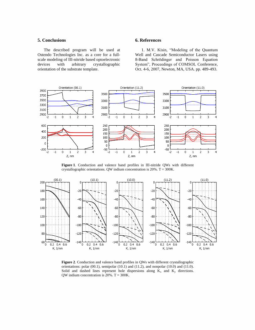
Figure 3 compares the QW material gain
spectra in structures with polar, semipolar, and
nonpolar orientations. For each orientation, the
subplots show the gain evolution with the
increasing QW width. In the nonpolar structure,
the red shift of the gain spectrum is related to the
decrease of the carrier confinement energy, while
the decline of the peak gain should be attributed
to the decrease in the hole subband separation;
see Figure 4 for subband dispersion evolution.
The latter trend leads to thermal hole
redistribution at elevated temperatures and
correspondingly degrades the optical gain. In
semipolar and, especially, in polar structures, the
gain deterioration is also affected by the
decreasing wave function overlap in wider QWs;
see Figure 5 which shows spatial redistribution
of the electron and hole states in the semipolar
(11.2) structure with increasing QW width. QW
indium concentration is 30% and the injection
level corresponds to the QW transparency point.
Weak screening of the piezoelectric field by the
injected carriers is noticeable in the wider QWs.
Figure 6 shows red shift of the QW optical
gain spectra in QWs with increasing indium
concentration. This shift is determined by strong
dependence of the GaInN band gap on the
Indium contents. Figure 7 illustrates the
temperature-induced red shift of the optical
spectra due to the band gap temperature
dependence. In Figure 7, the spontaneous
emission rate is compared with the stimulated
emission rate per one photon in the cavity. Light
with Y-polarization, depressed in the gain
spectra, is fully represented in the spontaneous
emission. Low value of the optical broadening
(1 meV) was adopted for this calculation to
resolve the spectral features. Spectral integration
of the spontaneous emission rates defines the
value of the QW effective radiative
recombination coefficient B, which includes the
effect of electron-hole spatial separation. At
temperature 75C the corresponding values of B
coefficient were obtained as (0.0045, 0.66, and
0.83)x10-10
cm3/s for polar, semipolar and
nonpolar QW structures respectively.
5. Conclusions
The described program will be used at
Ostendo Technologies Inc. as a core for a full-
scale modeling of III-nitride based optoelectronic
devices with arbitrary crystallographic
orientation of the substrate template.
6. References
1. M.V. Kisin, “Modeling of the Quantum
Well and Cascade Semiconductor Lasers using
8-Band Schrödinger and Poisson Equation
System”, Proceedings of COMSOL Conference,
Oct. 4-6, 2007, Newton, MA, USA. pp. 489-493.
Figure 1. Conduction and valence band profiles in III-nitride QWs with different
crystallographic orientations. QW indium concentration is 20%. T = 300K.
Figure 2. Conduction and valence band profiles in QWs with different crystallographic
orientations: polar (00.1), semipolar (10.1) and (11.2), and nonpolar (10.0) and (11.0).
Solid and dashed lines represent hole dispersions along Kx and Ky directions.
QW indium concentration is 20%. T = 300K.
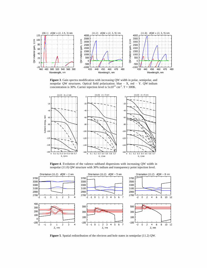
Figure 3. Gain spectra modification with increasing QW width in polar, semipolar, and
nonpolar QW structures. Optical field polarization: blue – X, red – Y. QW indium
concentration is 30%. Carrier injection level is 5x1012 cm-2. T = 300K.
Figure 4. Evolution of the valence subband dispersions with increasing QW width in
nonpolar (11.0) QW structure with 30% indium and transparency point injection level.
Figure 5. Spatial redistribution of the electron and hole states in semipolar (11.2) QW.
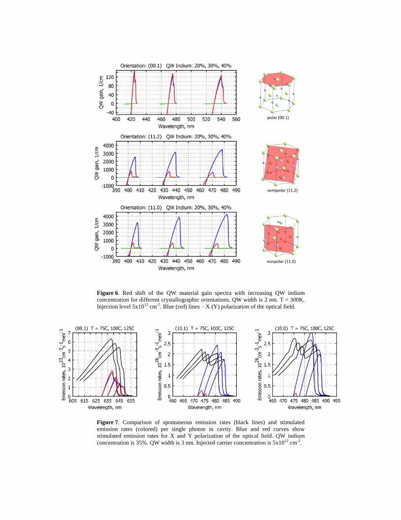
Figure 6. Red shift of the QW material gain spectra with increasing QW indium
concentration for different crystallographic orientations. QW width is 2 nm. T = 300K.
Injection level 5x1012 cm-2. Blue (red) lines – X (Y) polarization of the optical field.
Figure 7. Comparison of spontaneous emission rates (black lines) and stimulated
emission rates (colored) per single photon in cavity. Blue and red curves show
stimulated emission rates for X and Y polarization of the optical field. QW indium
concentration is 35%. QW width is 3 nm. Injected carrier concentration is 5x1012 cm-2.
polar (00.1)
semipolar (11.2)
nonpolar (11.0)