e33 743 e34 ds - rs components · single-chip z8 ® mcu family featuring enhanced wake-up...
TRANSCRIPT

1
PRELIMINARY PRODUCT SPECIFICATION
Z86E33/733/E34 Z86E43/743/E44 1
CMOS Z8 OTP MICROCONTROLLERS
FEATURES
Standard Temperature (VCC = 3.5V to 5.5V)
Extended Temperature (VCC = 4.5V to 5.5V)
Available Packages:– 28-Pin DIP/SOIC/PLCC OTP (E33/733/E34)
– 40-Pin DIP OTP (E43/743/E44)
– 44-Pin PLCC/QFP OTP (E43/743/E44)
Software Enabled Watch-Dog Timer (WDT)
Push-Pull/Open-Drain Programmable onPort 0, Port 1, and Port 2
24/32 Input/Output Lines
Clock-Free WDT Reset
Auto Power-On Reset (POR)
Programmable OTP Options:– RC Oscillator
– EPROM Protect
– Auto Latch Disable
– Permanently Enabled WDT
– Crystal Oscillator Feedback Resistor Disable
– RAM Protect
Low-Power Consumption: 60 mW
Fast Instruction Pointer: 0.75 µs
Two Standby Modes: STOP and HALT
Digital Inputs CMOS Levels, Schmitt-Triggered
Software Programmable Low EMI Mode
Two Programmable 8-Bit Counter/Timers Each with a6-Bit Programmable Prescaler
Six Vectored, Priority Interrupts from Six DifferentSources
Two Comparators
On-Chip Oscillator that Accepts a Crystal, CeramicResonator, LC, RC, or External Clock Drive
GENERAL DESCRIPTION
The Z86E33/733/E34/E43/743/E44 8-Bit One-Time Pro-grammable (OTP) Microcontrollers are members of Zilog'ssingle-chip Z8® MCU family featuring enhanced wake-upcircuitry, programmable Watch-Dog Timers, Low NoiseEMI options, and easy hardware/software system expan-sion capability.
Four basic address spaces support a wide range of mem-ory configurations. The designer has access to three addi-tional control registers that allow easy access to registermapped peripheral and I/O circuits.
For applications demanding powerful I/O capabilities, theZ86E33/733/E34 have 24 pins, and the Z86E43/743/E44have 32 pins of dedicated input and output. These lines are
DeviceROM (KB)
RAM*(Bytes)
I/O Lines
Speed(MHz)
Z86E33 4 237 24 12Z86733 8 237 24 12Z86E34 16 237 24 12Z86E43 4 236 32 12Z86743 8 236 32 12Z86E44 16 236 32 12
Note: *General-Purpose
DS97Z8X1500 P R E L I M I N A R Y 1

Z86E33/733/E34/E43/743/E44
CMOS Z8 OTP Microcontrollers Zilog
GENERAL DESCRIPTION
(Continued)
grouped into four ports, eight lines per port, and are con-figurable under software control to provide timing, statussignals, and parallel I/O with or without handshake, andaddress/data bus for interfacing external memory.
Notes: All signals with a preceding front slash, "/", areactive Low. For example, B//W (WORD is active Low);/B/W (BYTE is active Low, only).
Power connections follow conventional descriptions be-low:
Connection Circuit Device
Power VCC VDD
Ground GND VSS
Figure 1. Functional Block Diagram
Port 3
Counter/Timers (2)
InterruptControl
Two AnalogComparators
Port 2
I/O(Bit Programmable)
ALU
FLAGS
Machine Timing &
Instruction Control
ProgramCounter
VCC GND XTAL
4 4
Port 0
Output Input
Address or I/O(Nibble Programmable)
8
Address/Data or I/O(Byte Programmable)
/AS /DS R//W /RESET
RESETWDT, POR
Port 1
OTP
Register File
RegisterPointer
(E43/743/E44 Only)
(E43/743/E44 Only)
2 P R E L I M I N A R Y DS97Z8X1500

Z86E33/733/E34/E43/743/E44
Zilog CMOS Z8 OTP Microcontrollers
1
Figure 2. EPROM Programming Block Diagram
AddressMUX
EPROM
TEST ROM
OTPOptions
AD 11- 0
Z8 MCU
Address Counter
PGM + TestMode Logic
EPMP32
/CEXT1
/PGM P02
D7 - 0
AD 11- 0
AD 13- 0DataMUX
Z8Port 2
D7 - 0
/OEP31
VPPP33
D7 - 0
CLR(P00)
CLK(P01)
DS97Z8X1500 P R E L I M I N A R Y 3

Z86E33/733/E34/E43/743/E44
CMOS Z8 OTP Microcontrollers Zilog
PIN IDENTIFICATION
Figure 3. 40-Pin DIP Pin ConfigurationStandard Mode
R//wP25P26P27P04P05P06P14P15P07
VCCP16P17
XTAL2XTAL1
P31P32P33P34/AS
/DSP24P23P22P21P20P03P13P12GNDP02P11P10P01P00P30P36P37P35/RESET
40
DIP 40 - Pin
1
20 21
Table 1. 40-Pin DIP Pin IdentificationStandard Mode
Pin # Symbol Function Direction
1 R//W Read/Write Output2-4 P25-P27 Port 2, Pins 5,6,7 In/Output5-7 P04-P06 Port 0, Pins 4,5,6 In/Output8-9 P14-P15 Port 1, Pins 4,5 In/Output10 P07 Port 0, Pin 7 In/Output11 VCC Power Supply
12-13 P16-P17 Port 1, Pins 6,7 In/Output14 XTAL2 Crystal Oscillator Output15 XTAL1 Crystal Oscillator Input16-18 P31-P33 Port 3, Pins 1,2,3 Input19 P34 Port 3, Pin 4 Output20 /AS Address Strobe Output21 /RESET Reset Input22 P35 Port 3, Pin 5 Output23 P37 Port 3, Pin 7 Output24 P36 Port 3, Pin 6 Output25 P30 Port 3, Pin 0 Input26-27 P00-P01 Port 0, Pins 0,1 In/Output28-29 P10-P11 Port 1, Pins 0,1 In/Output30 P02 Port 0, Pin 2 In/Output31 GND Ground32-33 P12-P13 Port 1, Pins 2,3 In/Output34 P03 Port 0, Pin 3 In/Output35-39 P20-P24 Port 2, Pins 0,1,2,3,4 In/Output40 /DS Data Strobe Output
4 P R E L I M I N A R Y DS97Z8X1500

Z86E33/733/E34/E43/743/E44
Zilog CMOS Z8 OTP Microcontrollers
1
Figure 4. 44-Pin PLCC Pin ConfigurationStandard Mode
44-Pin PLCC
7
17
P21P22P23P24/DSNC
R//WP25P26P27P04
P30P36P37P35/RESETR//RL/ASP34P33P32P31
P05
P06
P14
P15
P07
VC
CV
CC
P16
P17
XTA
L2X
TAL1
P20
P03
P13
P12
GN
DG
ND
P02
P11
P10
P01
P00
1
2818
4039
29
6
Table 2. 44-Pin PLCC Pin Identification
Pin # Symbol Function Direction
1-2 GND Ground 3-4 P12-P13 Port 1, Pins 2,3 In/Output5 P03 Port 0, Pin 3 In/Output6-10 P20-P24 Port 2, Pins 0,1,2,3,4 In/Output11 /DS Data Strobe Output12 NC No Connection13 R//W Read/Write Output14-16 P25-P27 Port 2, Pins 5,6,7 In/Output17-19 P04-P06 Port 0, Pins 4,5,6 In/Output20-21 P14-P15 Port 1, Pins 4,5 In/Output22 P07 Port 0, Pin 7 In/Output23-24 VCC Power Supply 25-26 P16-P17 Port 1, Pins 6,7 In/Output27 XTAL2 Crystal Oscillator Output
28 XTAL1 Crystal Oscillator Input29-31 P31-P33 Port 3, Pins 1,2,3 Input32 P34 Port 3, Pin 4 Output33 /AS Address Strobe Output34 R//RL ROM/ROMless select Input35 /RESET Reset Input36 P35 Port 3, Pin 5 Output37 P37 Port 3, Pin 7 Output38 P36 Port 3, Pin 6 Output39 P30 Port 3, Pin 0 Input40-41 P00-P01 Port 0, Pins 0,1 In/Output42-43 P10-P11 Port 1, Pins 0,1 In/Output44 P02 Port 0, Pin 2 In/Output
Table 2. 44-Pin PLCC Pin Identification
Pin # Symbol Function Direction
DS97Z8X1500 P R E L I M I N A R Y 5

Z86E33/733/E34/E43/743/E44
CMOS Z8 OTP Microcontrollers Zilog
PIN IDENTIFICATION
(Continued)
Figure 5. 44-Pin QFP Pin ConfigurationStandard Mode
34
44
P21P22P23P24/DSNC
R//WP25P26P27P04
P30P36P37P35/RESETR//RL/ASP34P33P32P31
P05
P06
P14
P15
P07
VC
CV
CC
P16
P17
XTA
L2X
TAL1
P20
P03
P13
P12
GN
DG
ND
P02
P11
P10
P01
P00
1
2333
44-Pin QFP
11
22
12
Table 3. 44-Pin QFP Pin Identification
Pin # Symbol Function Direction
1-2 P05-P06 Port 0, Pins 5,6 In/Output3-4 P14-P15 Port 1, Pins 4,5 In/Output5 P07 Port 0, Pin 7 In/Output6-7 VCC Power Supply 8-9 P16-P17 Port 1, Pins 6,7 In/Output10 XTAL2 Crystal Oscillator Output11 XTAL1 Crystal Oscillator Input12-14 P31-P33 Port 3, Pins 1,2,3 Input15 P34 Port 3, Pin 4 Output16 /AS Address Strobe Output17 R//RL ROM/ROMless select Input18 /RESET Reset Input19 P35 Port 3, Pin 5 Output20 P37 Port 3, Pin 7 Output21 P36 Port 3, Pin 6 Output
22 P30 Port 3, Pin 0 Input23-24 P00-P01 Port 0, Pin 0,1 In/Output25-26 P10-P11 Port 1, Pins 0,1 In/Output27 P02 Port 0, Pin 2 In/Output28-29 GND Ground30-31 P12-P13 Port 1, Pins 2,3 In/Output32 P03 Port 0, Pin 3 In/Output33-37 P20-24 Port 2, Pins 0,1,2,3,4 In/Output38 /DS Data Strobe Output39 NC No Connection40 R//W Read/Write Output41-43 P25-P27 Port 2, Pins 5,6,7 In/Output44 P04 Port 0, Pin 4 In/Output
Table 3. 44-Pin QFP Pin Identification
Pin # Symbol Function Direction
6 P R E L I M I N A R Y DS97Z8X1500

Z86E33/733/E34/E43/743/E44
Zilog CMOS Z8 OTP Microcontrollers
1
Figure 6. 40-Pin DIP Pin ConfigurationEPROM Mode
NCD5D6D7NCNCNCNCNCNC
VCCNCNCNC/CE/OE
EPMVPP
NCNC
NCD4D3D2D1D0NCNCNCGND/PGMNCNCCLKCLRNCNCNCNCNC
40
40-Pin DIP
1
20 21
Table 4. 40-Pin DIP Package Pin IdentificationEPROM Mode
Pin # Symbol Function Direction
1 NC No Connection2-4 D5-D7 Data 5,6,7 In/Output5-10 NC No Connection11 VCC Power Supply
12-14 NC No Connection15 /CE Chip Select Input16 /OE Output Enable Input17 EPM EPROM Prog. Mode Input18 VPP Prog. Voltage Input19-25 NC No Connection26 CLR Clear Input27 CLK Clock Input28-29 NC No Connection30 /PGM Prog. Mode Input31 GND Ground32-34 NC No Connection35-39 D0-D4 Data 0,1,2,3,4 In/Output40 NC No Connection
DS97Z8X1500 P R E L I M I N A R Y 7

Z86E33/733/E34/E43/743/E44
CMOS Z8 OTP Microcontrollers Zilog
PIN IDENTIFICATION
(Continued)
Figure 7. 44-Pin PLCC Pin ConfigurationEPROM Programming Mode
44 -Pin PLCC
7
17
D1D2D3D4NCNCNCD5D6D7NC
NCNCNCNCNCNCNCNCVPPEPM/OE
NC
NC
NC
NC
NC
VC
CV
CC
NC
NC
NC
/CE
D0
NC
NC
NC
GN
DG
ND
/PG
MN
CN
CC
LKC
LR
1
2818
4039
29
6
Table 5. 44-Pin PLCC Pin ConfigurationEPROM Programming Mode
Pin # Symbol Function Direction
1-2 GND Ground3-5 NC No Connection6-10 D0-D4 Data 0,1,2,3,4 In/Output11-13 NC No Connection14-16 D5-D7 Data 5,6,7 In/Output17-22 NC No Connection23-24 VCC Power Supply25-27 NC No Connection28 /CE Chip Select Input
29 /OE Output Enable Input30 EPM EPROM Prog.
ModeInput
31 VPP Prog. Voltage Input
32-39 NC No Connection40 CLR Clear Input41 CLK Clock Input42-43 NC No Connection44 /PGM Prog. Mode Input
Table 5. 44-Pin PLCC Pin ConfigurationEPROM Programming Mode
Pin # Symbol Function Direction
8 P R E L I M I N A R Y DS97Z8X1500

Z86E33/733/E34/E43/743/E44
Zilog CMOS Z8 OTP Microcontrollers
1
Figure 8. 44-Pin QFP Pin ConfigurationEPROM Programming Mode
34
44
D1D2D3D4NCNCNCD5D6D7NC
NCNCNCNCNCNCNCNCVPPEPM/OE
NC
NC
NC
NC
NC
VC
CV
CC
NC
NC
NC
/CE
D0
NC
NC
NC
GN
DG
ND
/PG
MN
CN
CC
LKC
LR
1
2333
44 -Pin QFP
11
22
12
Table 6. 44-Pin QFP Pin IdentificationEPROM Programming Mode
Pin # Symbol Function Direction
1-5 NC No Connection6-7 VCC Power Supply
8-10 NC No Connection11 /CE Chip Select Input12 /OE Output Enable Input13 EPM EPROM Prog.
ModeInput
14 VPP Prog. Voltage Input
15-22 NC No Connection23 CLR Clear Input
24 CLK Clock Input25-26 NC No Connection27 /PGM Prog. Mode Input28-29 GND Ground30-32 NC No Connection33-37 D0-D4 Data 0,1,2,3,4 In/Output38-40 NC No Connection41-43 D5-D7 Data 5,6,7 In/Output44 NC No Connection
Table 6. 44-Pin QFP Pin IdentificationEPROM Programming Mode
Pin # Symbol Function Direction
DS97Z8X1500 P R E L I M I N A R Y 9

Z86E33/733/E34/E43/743/E44
CMOS Z8 OTP Microcontrollers Zilog
PIN IDENTIFICATION
(Continued)
Figure 9. Standard Mode28-Pin DIP/SOIC Pin Configuration
Table 7. 28-Pin DIP/SOIC/PLCCPin IdentificationStandard Mode
Pin # Symbol Function Direction
1-3 P25-P27 Port 2, Pins 5,6, In/Output4-7 P04-P07 Port 0, Pins 4,5,6,7 In/Output8 VCC Power Supply
9 XTAL2 Crystal Oscillator Output10 XTAL1 Crystal Oscillator Input11-13 P31-P33 Port 3, Pins 1,2,3 Input14-15 P34-P35 Port 3, Pins 4,5 Output16 P37 Port 3, Pin 7 Output17 P36 Port 3, Pin 6 Output18 P30 Port 3, Pin 0 Input19-21 P00-P02 Port 0, Pins 0,1,2 In/Output22 VSS Ground
23 P03 Port 0, Pin 3 In/Output24-28 P20-P24 Port 2, Pins
0,1,2,3,4In/Output
P25P26P27P04P05P06P07
VCCXTAL2XTAL1
P31P32P33P34
P24P23P22P21P20P03VSSP02P01P00P30P36P37P35
28
28-Pin DIP/SOIC
1
14 15
Figure 10. Standard Mode28-Pin PLCC Pin Configuration
25
19
5
111812
264
28-Pin PLCC
1XXXXXXXXXXXXXXXXXXXXX
XXXXXXXXXXXXXXXXXXXXX
P21P20P03VSSP02P01P00
P05P06P07
VCCXT2XT1P31
P04
P27
P26
P25
P24
P23
P22
P32
P33
P34
P35
P37
P36
P30
10 P R E L I M I N A R Y DS97Z8X1500

Z86E33/733/E34/E43/743/E44Zilog CMOS Z8 OTP Microcontrollers
1
Figure 11. EPROM Programming Mode28-Pin DIP/SOIC Pin Configuration
Figure 12. EPROM Programming Mode28-Pin PLCC Pin Configuration
D5D6D7NCNCNCNC
VCCNC/CE/OE
EPMVPP
NC
D4D3D2D1D0NCVSS/PGMCLKCLRNCNCNCNC
28
28-Pin DIP/SOIC
1
14 15
25
19
5
111812
264
28-Pin PLCC
1XXXXXXXXXXXXXXXXXXXXX
XXXXXXXXXXXXXXXXXXXXX
D1D0NCVSS/PGMCLKCLR
NCNCNC
VCCNC/CE/OE
NC
D7
D6
D5
D4
D3
D2
EP
MV
PP
NC
NC
NC
NC
NC
Table 8. 28-Pin EPROM Pin Identification
EPROM Mode
Pin # Symbol Function Direction
1-3 D5-D7 Data 5,6,7 In/Output4-7 NC No Connection8 VCC Power Supply
9 NC No connection10 /CE Chip Select Input11 /OE Output Enable Input12 EPM EPROM Prog.
ModeInput
13 VPP Prog. Voltage Input
14-18 NC No Connection19 CLR Clear20 CLK Clock21 /PGM Prog. Mode Input22 VSS Ground
23 NC No Connection24-28 D0-D4 Data 0,1,2,3,4 In/Output
DS97Z8X1500 P R E L I M I N A R Y 11

Z86E33/733/E34/E43/743/E44CMOS Z8 OTP Microcontrollers Zilog
ABSOLUTE MAXIMUM RATINGS
Stresses greater than those listed under Absolute Maxi-mum Ratings may cause permanent damage to the de-vice. This is a stress rating only; functional operation of thedevice at any condition above those indicated in the oper-ational sections of these specifications is not implied. Ex-posure to absolute maximum rating conditions for an ex-tended period may affect device reliability.
Total power dissipation should not exceed 1.2 W for thepackage. Power dissipation is calculated as follows:
Total Power Dissipation = VDD x [ IDD – (sum of IOH) ]+ sum of [ (VDD – VOH) x IOH ]+ sum of (V0L x I0L)
STANDARD TEST CONDITIONS
The characteristics listed below apply for standard testconditions as noted. All voltages are referenced toGround. Positive current flows into the referenced pin(Test Load).
Parameter Min Max Units
Ambient Temperature under Bias –40 +105 CStorage Temperature –65 +150 CVoltage on any Pin with Respect to VSS [Note 1] –0.6 +7 V
Voltage on VDD Pin with Respect to VSS –0.3 +7 V
Voltage on XTAL1, P32, P33 and /RESET Pins with Respect to VSS [Note 2]
–0.6 VDD+1 V
Total Power Dissipation 1.21 WMaximum Allowable Current out of VSS 220 mA
Maximum Allowable Current into VDD 180 mA
Maximum Allowable Current into an Input Pin [Note 3] –600 +600 µAMaximum Allowable Current into an Open-Drain Pin [Note 4] –600 +600 µAMaximum Allowable Output Current Sunk by Any I/O Pin 25 mAMaximum Allowable Output Current Sourced by Any I/O Pin 25 mAMaximum Allowable Output Current Sunk by /RESET Pin 3 mA
Notes: 1. This applies to all pins except XTAL pins and where otherwise noted.2. There is no input protection diode from pin to VDD.3. This excludes XTAL pins.4. Device pin is not at an output Low state.
Figure 13. Test Load Diagram
150 pF
From OutputUnder Test
12 P R E L I M I N A R Y DS97Z8X1500

Z86E33/733/E34/E43/743/E44Zilog CMOS Z8 OTP Microcontrollers
1
CAPACITANCETA = 25°C, VCC = GND = 0V, f = 1.0 MHz; unmeasured pins returned to GND.
DC ELECTRICAL CHARACTERISTICS
Parameter Min Max
Input capacitance 0 12 pFOutput capacitance 0 12 pFI/O capacitance 0 12 pF
TA= 0 °C to +70 °C
Sym ParameterVCC
Note [3] Min MaxTypical @ 25°C Units Conditions Notes
VCH Clock Input High Voltage 3.5V5.5V
0.7 VCC0.7 VCC
VCC+0.3VCC+0.3
1.82.5
VV
Driven by External Clock Generator
VCL Clock Input Low Voltage 3.5V5.5V
GND-0.3GND-0.3
0.2 VCC0.2 VCC
0.91.5
VV
Driven by External Clock Generator
VIH Input High Voltage 3.5V5.5V
0.7 VCC0.7 VCC
VCC+0.3VCC+0.3
2.52.5
VV
VIL Input Low Voltage 3.5V5.5V
GND-0.3GND-0.3
0.2 VCC0.2 VCC
1.51.5
VV
VOH Output High VoltageLow EMI Mode
3.5V5.5V
VCC–0.4VCC -0.4
3.34.8
VV
IOH = – 0.5 mA
VOH1 Output High Voltage 3.5V5.5V
VCC–0.4VCC–0.4
3.34.8
VV
IOH = -2.0 mAIOH = -2.0 mA
VOL Output Low VoltageLow EMI Mode
3.5V5.5V
0.40.4
0.20.2
VV
IOL = +1.0 mAIOL = +1.0 mA
VOL1 Output Low Voltage 3.5V5.5V
0.40.4
0.10.1
VV
IOL = + 4.0 mAIOL = + 4.0 mA
88
VOL2 Output Low Voltage 3.5V5.5V
1.21.2
0.50.5
VV
IOL = + 10 mAIOL = + 10 mA
88
VRH Reset Input High Voltage
3.5V5.5V
.8 VCC
.8 VCC
VCCVCC
1.72.1
VV
1313
VRL Reset Input Low Voltage 3.5V5.5V
GND –0.3GND –0.3
0.2 VCC0.2 VCC
1.31.7
VV
1313
VOLR Reset Output Low Voltage
3.5V5.5V
0.60.6
0.30.2
VV
IOL = +1.0 mAIOL = +1.0 mA
1313
VOFFSET Comparator Input Offset Voltage
3.5V5.5V
2525
1010
mVmV
VICR Input Common Mode Voltage Range
3.5V5.5V
00
VCC -1.0VVCC -1.0V
VV
1010
IIL Input Leakage 3.5V5.5V
–1–1
22
0.0320.032
µAµA
VIN = 0V, VCCVIN = 0V, VCC
IOL Output Leakage 3.5V5.5V
–1-1
22
0.0320.032
µAµA
VIN = 0V, VCCVIN = 0V, VCC
DS97Z8X1500 P R E L I M I N A R Y 13

Z86E33/733/E34/E43/743/E44CMOS Z8 OTP Microcontrollers Zilog
DC ELECTRICAL CHARACTERISTICS (Continued)
IIR Reset Input Current 3.5V5.5V
–20–20
–130–180
–65–112
µAµA
ICC Supply Current 3.5V5.5V
1520
515
mAmA
@ 12 MHz@ 12 MHz
4,54,5
ICC1 Standby CurrentHalt Mode
3.5V5.5V
46
24
mAmA
VIN = 0V, VCC @ 12 MHz
4,54,5
3.5V5.5V
35
1.53
mAmA
Clock Divide by 16 @ 12 MHz
4,54,5
ICC2 Standby CurrentStop Mode
3.5V5.5V3.5V5.5V
10101530
23710
µAµAµAµA
VIN = 0V, VCC VIN = 0V, VCCVIN = 0V, VCCVIN = 0V, VCC
6,116,11
6,11,146,11,14
IALL Auto LatchLow Current
3.5V5.5V
0.71.4
815
2.44.7
µAµA
0V <VIN<VCC0V <VIN<VCC
99
IALH Auto LatchHigh Current
3.5V5.5V
–0.6–1
–5–8
–1.8–3.8
µAµA
0V<VIN<VCC0V<VIN<VCC
99
TPOR Power On Reset 3.5V5.5V
3.02.0
2413
74
msms
VLV Auto Reset Voltage 2.3 3.0 2.8 V 1,7
Notes: 1. Device does function down to the Auto Reset voltage.2. GND=0V3. The VCC voltage specification of 5.5V guarantees 5.0V ± 0.5V and
the VCC voltage specification of 3.5V guarantees only 3.5V.4. All outputs unloaded, I/O pins floating, inputs at rail.5. CL1= CL2 = 22 pF6. Same as note [4] except inputs at VCC.7. Max. temperature is 70°C.8. STD Mode (not Low EMI Mode)9. Auto Latch (mask option) selected
10. For analog comparator inputs when analog comparators are enabled.
11. Clock must be forced Low, when XTAL1 is clock driven and XTAL2is floating.
12. Typicals are at VCC = 5.0V and VCC = 3.5V13. Z86E43/743/E44 only.14. WDT running
TA= 0 °C to +70 °C
Sym ParameterVCC
Note [3] Min MaxTypical @ 25°C Units Conditions Notes
14 P R E L I M I N A R Y DS97Z8X1500
Z86E33/733/E34/E43/743/E44Zilog CMOS Z8 OTP Microcontrollers
1
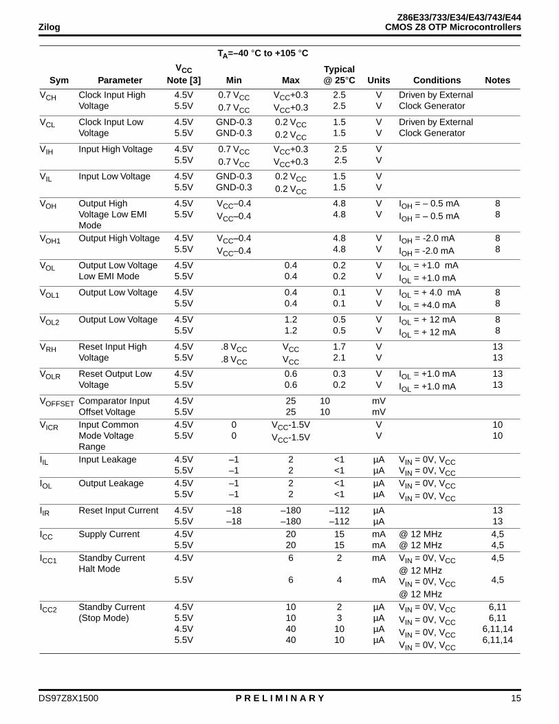
TA=–40 °C to +105 °CSym ParameterVCC
Note [3] Min MaxTypical @ 25°C Units Conditions Notes
VCH Clock Input High Voltage
4.5V5.5V
0.7 VCC0.7 VCC
VCC+0.3VCC+0.3
2.52.5
VV
Driven by External Clock Generator
VCL Clock Input Low Voltage
4.5V5.5V
GND-0.3GND-0.3
0.2 VCC0.2 VCC
1.51.5
VV
Driven by External Clock Generator
VIH Input High Voltage 4.5V5.5V
0.7 VCC0.7 VCC
VCC+0.3VCC+0.3
2.5 2.5
VV
VIL Input Low Voltage 4.5V5.5V
GND-0.3GND-0.3
0.2 VCC0.2 VCC
1.51.5
VV
VOH Output High Voltage Low EMI Mode
4.5V5.5V
VCC–0.4VCC–0.4
4.84.8
VV
IOH = – 0.5 mAIOH = – 0.5 mA
88
VOH1 Output High Voltage 4.5V5.5V
VCC–0.4VCC–0.4
4.84.8
VV
IOH = -2.0 mAIOH = -2.0 mA
88
VOL Output Low Voltage Low EMI Mode
4.5V5.5V
0.40.4
0.20.2
VV
IOL = +1.0 mAIOL = +1.0 mA
VOL1 Output Low Voltage 4.5V5.5V
0.40.4
0.10.1
VV
IOL = + 4.0 mAIOL = +4.0 mA
88
VOL2 Output Low Voltage 4.5V5.5V
1.21.2
0.50.5
VV
IOL = + 12 mAIOL = + 12 mA
88
VRH Reset Input High Voltage
4.5V5.5V
.8 VCC
.8 VCC
VCCVCC
1.72.1
VV
1313
VOLR Reset Output Low Voltage
4.5V5.5V
0.60.6
0.30.2
VV
IOL = +1.0 mAIOL = +1.0 mA
1313
VOFFSET Comparator Input Offset Voltage
4.5V5.5V
2525
1010
mVmV
VICR Input Common Mode Voltage Range
4.5V5.5V
00
VCC-1.5VVCC-1.5V
VV
1010
IIL Input Leakage 4.5V5.5V
–1–1
22
<1<1
µAµA
VIN = 0V, VCCVIN = 0V, VCC
IOL Output Leakage 4.5V5.5V
–1–1
22
<1<1
µAµA
VIN = 0V, VCCVIN = 0V, VCC
IIR Reset Input Current 4.5V5.5V
–18–18
–180–180
–112–112
µAµA
1313
ICC Supply Current 4.5V5.5V
2020
1515
mAmA
@ 12 MHz@ 12 MHz
4,54,5
ICC1 Standby CurrentHalt Mode
4.5V
5.5V
6
6
2
4
mA
mA
VIN = 0V, VCC @ 12 MHzVIN = 0V, VCC @ 12 MHz
4,5
4,5
ICC2 Standby Current(Stop Mode)
4.5V5.5V4.5V5.5V
10104040
231010
µAµAµAµA
VIN = 0V, VCCVIN = 0V, VCCVIN = 0V, VCCVIN = 0V, VCC
6,116,11
6,11,146,11,14
DS97Z8X1500 P R E L I M I N A R Y 15

Z86E33/733/E34/E43/743/E44CMOS Z8 OTP Microcontrollers Zilog
DC ELECTRICAL CHARACTERISTICS (Continued)
IALL Auto Latch Low Current
4.5V5.5V
1.41.4
2020
4.74.7
µAµA
0V < VIN < VCC0V < VIN < VCC
99
IALH Auto Latch High Current
4.5V5.5V
–1.0–1.0
–10–10
–3.8–3.8
µAµA
0V < VIN < VCC0V < VIN < VCC
99
TPOR Power On Reset 4.5V5.5V
2.02.0
1414
44
msms
VLV Auto Reset Voltage 2.0 3.3 2.8 V 1
1. Device does function down to the Auto Reset voltage.2. GND=0V3. The VCC voltage specification of 5.5V guarantees 5.0V ± 0.5V.4. All outputs unloaded, I/O pins floating, inputs at rail.5. CL1= CL2 = 22 pF6. Same as note [4] except inputs at VCC.7. Maximum temperature is 70°C8. STD Mode (not Low EMI Mode)9. Auto Latch (mask option) selected
10. For analog comparator inputs when analog comparators are enabled.
11. Clock must be forced Low, when XTAL1 is clock driven and XTAL2 is floating.
12. Typicals are at VCC = 5.0V13. Z86E43/743/E44 only.14. WDT is not running.
TA=–40 °C to +105 °C
Sym ParameterVCC
Note [3] Min MaxTypical @ 25°C Units Conditions Notes
16 P R E L I M I N A R Y DS97Z8X1500

Z86E33/733/E34/E43/743/E44Zilog CMOS Z8 OTP Microcontrollers
1
Figure 14. External I/O or Memory Read/Write Timing(Z86E43/743/E44 Only)
R//W, /DM
9
12
18 3
16
13
4
5
8 11
6
17
10
15
7
14
21
Port 0
Port 1
/AS
/DS(Read)
Port1
/DS(W rite)
A7 - A0 D7 - D0 IN
D7 - D0 OUTA7 - A0
19
DS97Z8X1500 P R E L I M I N A R Y 17

Z86E33/733/E34/E43/743/E44CMOS Z8 OTP Microcontrollers Zilog
DC ELECTRICAL CHARACTERISTICS (Continued)
TA = 0°C to 70°C12 MHz
No Symbol ParameterNote [3]
VCC Min Max Units Notes
1 TdA(AS) Address Valid to /AS Rise Delay
3.5V5.5V
3535
nsns
22
2 TdAS(A) /AS Rise to Address Float Delay
3.5V5.5V
4545
nsns
22
3 TdAS(DR) /AS Rise to Read Data Req’d Valid
3.5V5.5V
250250
nsns
1,21,2
4 TwAS /AS Low Width 3.5V5.5V
5555
nsns
22
5 TdAS(DS) Address Float to /DS Fall 3.5V5.5V
00
nsns
6 TwDSR /DS (Read) Low Width 3.5V5.5V
200200
nsns
1,21,2
7 TwDSW /DS (Write) Low Width 3.5V5.5V
110110
nsns
1,21,2
8 TdDSR(DR) /DS Fall to Read Data Req’d Valid
3.5V5.5V
150150
nsns
1,21,2
9 ThDR(DS) Read Data to /DS Rise Hold Time
3.5V5.5V
00
nsns
22
10 TdDS(A) /DS Rise to Address Active Delay
3.5V5.5V
4555
nsns
22
11 TdDS(AS) /DS Rise to /AS Fall Delay 3.5V5.5V
3045
nsns
22
12 TdR/W(AS) R//W Valid to /AS Rise Delay
3.5V5.5V
4545
nsns
22
13 TdDS(R/W) /DS Rise to R//W Not Valid 3.5V5.5V
4545
nsns
22
14 TdDW(DSW) Write Data Valid to /DS Fall (Write) Delay
3.5V5.5V
5555
nsns
22
15 TdDS(DW) /DS Rise to Write Data Not Valid Delay
3.5V5.5V
4555
nsns
22
16 TdA(DR) Address Valid to Read Data Req’d Valid
3.5V5.5V
310310
nsns
1,21,2
17 TdAS(DS) /AS Rise to /DS Fall Delay 3.5V5.5V
6565
nsns
22
18 TdDM(AS) /DM Valid to /AS Rise Delay 3.5V5.5V
3535
nsns
22
19 ThDS(AS) /DS Valid to Address Valid Hold Time
3.5V5.5V
3535
nsns
22
Notes: 1. When using extended memory timing, add 2 TpC.2. Timing numbers given are for minimum TpC.3. The VCC voltage specification of 5.5V guarantees 5.0V ±0.5V and
the VCC voltage specification of 3.5V guarantees only 3.5VStandard Test LoadAll timing references use 0.7 VCC for a logic 1 and 0.2 VCC for a logic 0.For Standard Mode (not Low-EMI Mode for outputs) with SMR D1 = 0, D0 = 0.
18 P R E L I M I N A R Y DS97Z8X1500

Z86E33/733/E34/E43/743/E44Zilog CMOS Z8 OTP Microcontrollers
1
TA = -40°C to 105°C12 MHz
No Symbol ParameterNote [3]
VCC Min Max Units Notes
1 TdA(AS) Address Valid to /AS Rise Delay
4.5V5.5V
3535
nsns
22
2 TdAS(A) /AS Rise to Address Float Delay
4.5V5.5V
4545
nsns
22
3 TdAS(DR) /AS Rise to Read Data Req’d Valid
4.5V5.5V
250250
nsns
1,21,2
4 TwAS /AS Low Width 4.5V5.5V
5555
nsns
22
5 TdAS(DS) Address Float to /DS Fall 4.5V5.5V
00
nsns
6 TwDSR /DS (Read) Low Width 4.5V5.5V
200200
nsns
1,21,2
7 TwDSW /DS (Write) Low Width 4.5V5.5V
110110
nsns
1,21,2
8 TdDSR(DR) /DS Fall to Read Data Req’d Valid
4.5V5.5V
150150
nsns
1,21,2
9 ThDR(DS) Read Data to /DS Rise Hold Time
4.5V5.5V
00
nsns
22
10 TdDS(A) /DS Rise to Address Active Delay
4.5V5.5V
4555
nsns
22
11 TdDS(AS) /DS Rise to /AS Fall Delay 4.5V5.5V
4545
nsns
22
12 TdR/W(AS) R//W Valid to /AS Rise Delay
4.5V5.5V
4545
nsns
22
13 TdDS(R/W) /DS Rise to R//W Not Valid 4.5V5.5V
4545
nsns
22
14 TdDW(DSW) Write Data Valid to /DS Fall (Write) Delay
4.5V5.5V
5555
nsns
22
15 TdDS(DW) /DS Rise to Write Data Not Valid Delay
4.5V5.5V
5555
nsns
22
16 TdA(DR) Address Valid to Read Data Req’d Valid
4.5V5.5V
310310
nsns
1,21,2
17 TdAS(DS) /AS Rise to /DS Fall Delay 4.5V5.5V
6565
nsns
22
18 TdDM(AS) /DM Valid to /AS Rise Delay 4.5V5.5V
3535
nsns
22
19 ThDS(AS) /DS Valid to Address Valid Hold Time
4.5V5.5V
3535
nsns
22
Notes: 1. When using extended memory timing, add 2 TpC.2. Timing numbers given are for minimum TpC.3. The VCC voltage specification of 5.5V guarantees 5.0V ± 0.5V and
the VCC voltage specification of 3.5V guarantees only 3.5VStandard Test LoadAll timing references use 0.7 VCC for a logic 1 and 0.2 VCC for a logic 0.For Standard Mode (not Low-EMI Mode for outputs) with SMR, D1 = 0, D0 = 0.
DS97Z8X1500 P R E L I M I N A R Y 19

Z86E33/733/E34/E43/743/E44CMOS Z8 OTP Microcontrollers Zilog
DC ELECTRICAL CHARACTERISTICS (Continued)
Figure 15. Additional Timing Diagram
Clock
1 3
4
8
2 2 3
TIN
IRQN
6
5
7 7
11
ClockSetup
10
9
Stop Mode
Recovery Source
20 P R E L I M I N A R Y DS97Z8X1500

Z86E33/733/E34/E43/743/E44Zilog CMOS Z8 OTP Microcontrollers
1
Additional Timing Table (Divide-By-One Mode)
TA = 0 °C to +70 °C
4 MHz 6 MHz
No Symbol ParameterVCC
Note [6] Min Max Min Max Units Notes
1 TpC Input Clock Period 3.5V5.5V
250250
DC DC
166166
DCDC
nsns
1,7,81,7,8
2 TrC,TfC Clock Input Rise & Fall Times
3.5V5.5V
2525
2525
nsns
1,7,81,7,8
3 TwC Input Clock Width 3.5V5.5V
100100
100100
nsns
1,7,81,7,8
4 TwTinL Timer Input Low Width
3.5V5.5V
100 70
10070
nsns
1,7,81,7,8
5 TwTinH Timer Input High Width
3.5V5.5V
5TpC5TpC
5TpC5TpC
1,7,81,7,8
6 TpTin Timer Input Period 3.5V5.5V
8TpC8TpC
8TpC8TpC
1,7,81,7,8
7 TrTin, TfTin Timer Input Rise & Fall Timer
3.5V5.5V
100100
100100
nsns
1,7,81,7,8
8A TwIL Int. Request Low Time
3.5V5.5V
10070
10070
nsns
1,2,7,81,2,7,8
8B TwIL Int. Request Low Time
3.5V5.5V
5TpC5TpC
5TpC5TpC
1,3,7,81,3,7,8
9 TwIH Int. Request Input High Time
3.5V5.5V
5TpC5TpC
5TpC5TpC
1,2,7,81,2,7,8
10 Twsm STOP Mode Recovery Width Spec
3.5V5.5V
1212
12 12
nsns
4,84,8
11 Tost Oscillator Startup Time
3.5V5.5V
5TpC5TpC
5TpC5TpC
4,8,94,8,9
Notes: 1. Timing Reference uses 0.7 VCC for a logic 1 and 0.2 VCC for a logic 0.2. Interrupt request via Port 3 (P31-P33).3. Interrupt request via Port 3 (P30).4. SMR-D5 = 1, POR STOP Mode Delay is on.5. Reg. WDTMR.6. The VCC voltage specification of 5.5V guarantees 5.0V ±0.5V and
the VCC voltage specification of 3.5V guarantees 3.5V only.7. SMR D1 = 0.8. Maximum frequency for internal system clock is 4 MHz when
using Low EMI OSC PCON Bit D7 = 0.9. For RC and LC oscillator, and for oscillator driven by clock driver.
DS97Z8X1500 P R E L I M I N A R Y 21

Z86E33/733/E34/E43/743/E44CMOS Z8 OTP Microcontrollers Zilog
Additional Timing Table (Divide-By-One Mode)
TA = -40 °C to +105 °C
4 MHz 6 MHz
No Symbol ParameterVCC
Note [6] Min Max Min Max Units Notes
1 TpC Input Clock Period 4.5V5.5V
250250
DC DC
166166
DCDC
nsns
1,7,81,7,8
2 TrC,TfC Clock Input Rise & Fall Times
4.5V5.5V
2525
2525
nsns
1,7,81,7,8
3 TwC Input Clock Width 4.5V5.5V
100100
100100
nsns
1,7,81,7,8
4 TwTinL Timer Input Low Width
4.5V5.5V
100 70
10070
nsns
1,7,81,7,8
5 TwTinH Timer Input High Width
4.5V5.5V
5TpC5TpC
5TpC5TpC
1,7,81,7,8
6 TpTin Timer Input Period 4.5V5.5V
8TpC8TpC
8TpC8TpC
1,7,81,7,8
7 TrTin, TfTin Timer Input Rise & Fall Timer
4.5V5.5V
100100
100100
nsns
1,7,81,7,8
8A TwIL Int. Request Low Time
4.5V5.5V
10070
10070
nsns
1,2,7,81,2,7,8
8B TwIL Int. Request Low Time
4.5V5.5V
5TpC5TpC
5TpC5TpC
1,3,7,81,3,7,8
9 TwIH Int. Request Input High Time
4.5V5.5V
5TpC5TpC
5TpC5TpC
1,2,7,81,2,7,8
10 Twsm STOP Mode Recovery Width Spec
4.5V5.5V
1212
12 12
nsns
4,84,8
11 Tost Oscillator Startup Time
4.5V5.5V
5TpC5TpC
5TpC5TpC
4,8,94,8,9
Notes: 1. Timing Reference uses 0.7 VCC for a logic 1 and 0.2 VCC for a logic 0.2. Interrupt request via Port 3 (P31-P33).3. Interrupt request via Port 3 (P30).4. SMR-D5 = 1, POR STOP Mode Delay is on.5. Reg. WDTMR.6. The VCC voltage specification of 5.5V guarantees 5.0V ±0.5V and
the VCC voltage specification of 3.5V guarantees 3.5V only.7. SMR D1 = 0.8. Maximum frequency for internal system clock is 4 MHz when
using Low EMI OSC PCON Bit D7 = 0.9. For RC and LC oscillator, and for oscillator driven by clock driver.
22 P R E L I M I N A R Y DS97Z8X1500

Z86E33/733/E34/E43/743/E44Zilog CMOS Z8 OTP Microcontrollers
1
Handshake Timing Diagrams
Figure 16. Input Handshake Timing
Data In
1 2
3
4 5 6
/DAV(Input)
RDY(Output)
Next Data In Valid
Delayed RDY
Delayed DAV
Data In Valid
Figure 17. Output Handshake Timing
Data Out
/DAV(Output)
RDY(Input)
Next Data Out Valid
Delayed RDY
Delayed DAV
Data Out Valid
7
8 9
10
11
DS97Z8X1500 P R E L I M I N A R Y 23

Z86E33/733/E34/E43/743/E44CMOS Z8 OTP Microcontrollers Zilog
Additional Timing Table (Divide by Two Mode)
TA = 0 °C to +70 °C
12 MHz 4 MHz
No Symbol ParameterVCC
Note [6] Min Max Min Max Units Conditions Notes
1 TpC Input Clock Period 3.5V5.5V
62.562.5
DC DC
250250
DCDC
nsns
1,7,81,7,8
2 TrC,TfC Clock Input Rise & Fall Times
3.5V5.5V
1515
2525
nsns
1,7,81,7,8
3 TwC Input Clock Width 3.5V5.5V
31 31
3131
nsns
1,7,81,7,8
4 TwTinL Timer Input Low Width
3.5V5.5V
7070
7070
nsns
1,7,81,7,8
5 TwTinH Timer Input High Width
3.5V5.5V
5TpC5TpC
5TpC5TpC
1,7,81,7,8
6 TpTin Timer Input Period 3.5V5.5V
8TpC 8TpC
8TpC8TpC
1,7,81,7,8
7 TrTin, TfTin Timer Input Rise & Fall Timer
3.5V5.5V
100100
100100
nsns
1,7,81,7,8
8A TwIL Int. Request Low Time
3.5V5.5V
7070
7070
nsns
1,2,7,81,2,7,8
8B TwIL Int. Request Low Time
3.5V5.5V
5TpC5TpC
5TpC5TpC
1,3,7,81,3,7,8
9 TwIH Int. Request Input High Time
3.5V5.5V
5TpC5TpC
5TpC5TpC
1,2,7,81,2,7,8
10 Twsm STOP Mode Recovery Width Spec
3.5V5.5V
1212
1212
nsns
4,84,8
11 Tost Oscillator Startup Time
3.5V5.5V
5TpC5TpC
5TpC5TpC
4,84,8
12 Twdt Watch-Dog Timer Delay Time Before Timeout
3.5V5.5V
105
105
msms
D0 = 0D1 = 0
5,11 5,11
3.5V5.5V
20 10
2010
msms
D0 = 1D1 = 0
5,11 5,11
3.5V5.5V
40 20
4020
msms
D0 = 0D1 = 1
5,11 5,11
3.5V5.5V
16080
16080
msms
D0 = 1D1 = 1
5,11 5,11
Notes: 1. Timing Reference uses 0.7 VCC for a logic 1 and 0.2 VCC for a logic 0.2. Interrupt request via Port 3 (P31-P33)3. Interrupt request via Port 3 (P30)4. SMR-D5 = 1, POR STOP Mode Delay is on5. Reg. WDTMR6. The VCC voltage specification of 5.5V guarantees 5.0V ±0.5V and
the VCC voltage specification of 3.5V guarantees 3.5V only.7. SMR D1 = 08. Maximum frequency for internal system clock is 2 MHz when using
Low EMI OSC PCON Bit D7 = 0.9. For RC and LC oscillator, and for oscillator driven by clock driver.
10. Standard Mode (not Low EMI output ports)11. Using internal RC
24 P R E L I M I N A R Y DS97Z8X1500

Z86E33/733/E34/E43/743/E44Zilog CMOS Z8 OTP Microcontrollers
1
Additional Timing Table (Divide by Two Mode)
TA = -40 °C to +105 °C
12 MHz 4 MHz
No Symbol ParameterVCC
Note [6] Min Max Min Max Units Conditions Notes
1 TpC Input Clock Period 4.5V5.5V
62.562.5
DC DC
250250
DCDC
nsns
1,7,81,7,8
2 TrC,TfC Clock Input Rise & Fall Times
4.5V5.5V
1515
2525
nsns
1,7,81,7,8
3 TwC Input Clock Width 4.5V5.5V
31 31
3131
nsns
1,7,81,7,8
4 TwTinL Timer Input Low Width
4.5V5.5V
7070
7070
nsns
1,7,81,7,8
5 TwTinH Timer Input High Width
4.5V5.5V
5TpC5TpC
5TpC5TpC
1,7,81,7,8
6 TpTin Timer Input Period 4.5V5.5V
8TpC 8TpC
8TpC8TpC
1,7,81,7,8
7 TrTin, TfTin Timer Input Rise & Fall Timer
4.5V5.5V
100100
100100
nsns
1,7,81,7,8
8A TwIL Int. Request Low Time
4.5V5.5V
7070
7070
nsns
1,2,7,81,2,7,8
8B TwIL Int. Request Low Time
4.5V5.5V
5TpC5TpC
5TpC5TpC
1,3,7,81,3,7,8
9 TwIH Int. Request Input High Time
4.5V5.5V
5TpC5TpC
5TpC5TpC
1,2,7,81,2,7,8
10 Twsm STOP Mode Recovery Width Spec
4.5V5.5V
1212
1212
nsns
4,84,8
11 Tost Oscillator Startup Time
4.5V5.5V
5TpC5TpC
5TpC5TpC
4,84,8
12 Twdt Watch-Dog Timer Delay Time Before Timeout
4.5V5.5V
55
55
msms
D0 = 0D1 = 0
5,11 5,11
4.5V5.5V
10 10
1010
msms
D0 = 1D1 = 0
5,11 5,11
4.5V5.5V
20 20
2020
msms
D0 = 0D1 = 1
5,11 5,11
4.5V5.5V
8080
8080
msms
D0 = 1D1 = 1
5,11 5,11
Notes: 1. Timing Reference uses 0.7 VCC for a logic 1 and 0.2 VCC for a logic 0.2. Interrupt request via Port 3 (P31-P33)3. Interrupt request via Port 3 (P30)4. SMR-D5 = 1, POR STOP Mode Delay is on5. Reg. WDTMR6. The VCC voltage specification of 5.5V guarantees 5.0V ±0.5V and
the VCC voltage specification of 3.5V guarantees 3.5V only.7. SMR D1 = 08. Maximum frequency for internal system clock is 2 MHz when using
Low EMI OSC PCON Bit D7 = 0.9. For RC and LC oscillator, and for oscillator driven by clock driver.
10. Standard Mode (not Low EMI output ports)11. Using internal RC
DS97Z8X1500 P R E L I M I N A R Y 25

Z86E33/733/E34/E43/743/E44CMOS Z8 OTP Microcontrollers Zilog
PIN FUNCTIONS
EPROM Programming ModeD7-D0 Data Bus. The data can be read from or written toexternal memory through the data bus.
VCC Power Supply. This pin must supply 5V during theEPROM read mode and 6V during other modes.
/CE Chip Enable (active Low). This pin is active duringEPROM Read Mode, Program Mode, and Program VerifyMode.
/OE Output Enable (active Low). This pin drives the direc-tion of the Data Bus. When this pin is Low, the Data Bus isoutput, when High, the Data Bus is input.
EPM EPROM Program Mode. This pin controls the differ-ent EPROM Program Mode by applying different voltages.
VPP Program Voltage. This pin supplies the program volt-age.
/PGM Program Mode (active Low). When this pin is Low,the data is programmed to the EPROM through the DataBus.
CLR Clear (active High). This pin resets the internal ad-dress counter at the High Level.
CLK Address Clock. This pin is a clock input. The internaladdress counter increases by one for each clock cycle.
Application PrecautionThe production test-mode environment may be enabledaccidentally during normal operation if excessive noisesurges above VCC occur on pins P31 and /RESET.
In addition, processor operation of Z8 OTP devices may beaffected by excessive noise surges on the VPP, EPM, /OEpins while the microcontroller is in Standard Mode.
Recommendations for dampening voltage surges in bothtest and OTP mode include the following:
Using a clamping diode to VCC
Adding a capacitor to the affected pin
Enable EPROM/Test Mode Disable OTP option bit.
Standard ModeXTAL Crystal 1 (time-based input). This pin connects aparallel-resonant crystal, ceramic resonator, LC, RC net-work, or external single-phase clock to the on-chip oscilla-tor input.
XTAL2 Crystal 2 (time-based output). This pin connects aparallel-resonant crystal, ceramic resonator, LC, or RCnetwork to the on-chip oscillator output.
R//W Read/Write (output, write Low). The R//W signal isLow when the CCP is writing to the external program ordata memory (Z86E43/743/E44 only).
/RESET Reset (input, active Low). Reset will initialize theMCU. Reset is accomplished either through Power-On,Watch-Dog Timer reset, STOP-Mode Recovery, or exter-nal reset. During Power-On Reset and Watch-Dog TimerReset, the internally generated reset drives the reset pinlow for the POR time. Any devices driving the reset linemust be open-drain in order to avoid damage from a pos-sible conflict during reset conditions. Pull-up is provided in-ternally. After the POR time, /RESET is a Schmitt-trig-gered input. (/Reset is available on Z86E43/743/E44 only.)
To avoid asynchronous and noisy reset problems, theZ86E43/743/E44 is equipped with a reset filter of four exter-nal clocks (4TpC). If the external reset signal is less than4TpC in duration, no reset occurs. On the fifth clock afterthe reset is detected, an internal RST signal is latched andheld for an internal register count of 18 external clocks, orfor the duration of the external reset, whichever is longer.During the reset cycle, /DS is held active Low while /AS cy-cles at a rate of TpC/2. Program execution begins at loca-tion 000CH, 5-10 TpC cycles after /RESET is released. ForPower-On Reset, the reset output time is 5 ms. TheZ86E43/743/E44 does not reset WDTMR, SMR, P2M, andP3M registers on a STOP-Mode Recovery operation.
/ROMless (input, active Low). This pin, when connected toGND, disables the internal ROM and forces the device tofunction as a Z86C90/C89 ROMless Z8. (Note that, whenleft unconnected or pulled High to VCC, the device func-tions normally as a Z8 ROM version).
Note: When using in ROM Mode in High EMI (noisy) envi-ronment, the ROMless pins should be connected directlyto VCC.
/DS (output, active Low). Data Strobe is activated once foreach external memory transfer. For a READ operation,data must be available prior to the trailing edge of /DS. ForWRITE operations, the falling edge of /DS indicates thatoutput data is valid.
/AS (output, active Low). Address Strobe is pulsed once atthe beginning of each machine cycle for external memorytransfer. Address output is from Port 0/Port 1 for all exter-nal programs. Memory address transfers are valid at thetrailing edge of /AS. Under program control, /AS is placedin the high-impedance state along with Ports 0 and 1, DataStrobe, and Read/Write.
26 P R E L I M I N A R Y DS97Z8X1500

Z86E33/733/E34/E43/743/E44Zilog CMOS Z8 OTP Microcontrollers
1
Port 0 (P07-P00). Port 0 is an 8-bit, bidirectional, CMOS-compatible I/O port. These eight I/O lines can be config-ured under software control as a nibble I/O port, or as anaddress port for interfacing external memory. The inputbuffers are Schmitt-triggered and nibble programmed. Ei-ther nibble output that can be globally programmed aspush-pull or open-drain. Low EMI output buffers can beglobally programmed by the software. Port 0 can be placedunder handshake control. In Handshake Mode, Port 3lines P32 and P35 are used as handshake control lines.The handshake direction is determined by the configura-tion (input or output) assigned to Port 0's upper nibble. Thelower nibble must have the same direction as the uppernibble.
For external memory references, Port 0 provides addressbits A11-A8 (lower nibble) or A15-A8 (lower and upper nib-ble) depending on the required address space. If the ad-dress range requires 12 bits or less, the upper nibble ofPort 0 can be programmed independently as I/O while thelower nibble is used for addressing. If one or both nibblesare needed for I/O operation, they must be configured bywriting to the Port 0 mode register. In ROMless mode, aftera hardware reset, Port 0 is configured as address linesA15-A8, and extended timing is set to accommodate slowmemory access. The initialization routine can include re-configuration to eliminate this extended timing mode. InROM mode, Port 0 is defined as input after reset.
Port 0 can be set in the High-Impedance Mode if selectedas an address output state, along with Port 1 and the con-trol signals /AS, /DS, and R//W (Figure 18).
Figure 18. Port 0 Configuration
Handshake Controls/DAV0 and RDY0(P32 and P35)
In
1.5 2.3V Hysteresis
PAD
Port 0 (I/O)
4
4
OEN
Out
Open-Drain
Auto Latch
R 500 kΩ
MCU
DS97Z8X1500 P R E L I M I N A R Y 27

Z86E33/733/E34/E43/743/E44CMOS Z8 OTP Microcontrollers Zilog
PIN FUNCTIONS (Continued)
Port 1 (P17-P10). Port 1 is an 8-bit, bidirectional, CMOS-compatible port with multiplexed Address (A7-A0) andData (D7-D0) ports. These eight I/O lines can be pro-grammed as inputs or outputs or can be configured undersoftware control as an Address/Data port for interfacingexternal memory. The input buffers are Schmitt-triggeredand the output buffers can be globally programmed as ei-ther push-pull or open-drain. Low EMI output buffers canbe globally programmed by the software. Port 1 can beplaced under handshake control. In this configuration, Port3, lines P33 and P34 are used as the handshake controls
RDY1 and /DAV1 (Ready and Data Available). To inter-face external memory, Port 1 must be programmed for themultiplexed Address/Data mode. If more than 256 externallocations are required, Port 0 outputs the additional lines(Figure 19).
Port 1 can be placed in the high-impedance state alongwith Port 0, /AS, /DS, and R//W, allowing theZ86E43/743/E44 to share common resources in multipro-cessor and DMA applications. In ROM mode, Port 1 is de-fined as input after reset.
Figure 19. Port 1 Configuration (Z86E43/743/E44 Only)
In
1.5 2.3V Hysteresis
PAD
OEN
Out
Open-Drain
Auto Latch
R 500 kΩ
Port 2 (I/O)
Handshake Controls/DAV1 and RDY1 (P33 and P34)
MCU
28 P R E L I M I N A R Y DS97Z8X1500

Z86E33/733/E34/E43/743/E44Zilog CMOS Z8 OTP Microcontrollers
1
Port 2 (P27-P20). Port 2 is an 8-bit, bidirectional, CMOS-compatible I/O port. These eight I/O lines can be config-ured under software control as an input or output, indepen-dently. All input buffers are Schmitt-triggered. Bits pro-grammed as outputs can be globally programmed aseither push-pull or open-drain. Low EMI output buffers canbe globally programmed by the software. When used as an
I/O port, Port 2 can be placed under handshake control. Af-ter reset, Port 2 is defined as an input.
In Handshake Mode, Port 3 lines P31 and P36 are used ashandshake control lines. The handshake direction is deter-mined by the configuration (input or output) assigned to bit7 of Port 2 (Figure 20).
Figure 20. Port 2 Configuration
OEN
Out
In
PAD
Port 2 (I/O)
Handshake Controls/DAV2 and RDY2 (P31 and P36)
MCU
Auto Latch
R ≈ 500 KΩ
Open-Drain
1.5 2.3V Hysteresis
DS97Z8X1500 P R E L I M I N A R Y 29

Z86E33/733/E34/E43/743/E44CMOS Z8 OTP Microcontrollers Zilog
PIN FUNCTIONS (Continued)
Port 3 (P37-P30). Port 3 is an 8-bit, CMOS-compatibleport with four fixed inputs (P33-P30) and four fixed outputs(P37-P34). These eight lines can be configured by soft-ware for interrupt and handshake control functions. Port 3,Pin 0 is Schmitt- triggered. P31, P32, and P33 are stan-dard CMOS inputs with single trip point (no Auto Latches)and P34, P35, P36, and P37 are push-pull output lines.Low EMI output buffers can be globally programmed bythe software. Two on-board comparators can process an-alog signals on P31 and P32 with reference to the voltageon P33. The analog function is enabled by setting the D1of Port 3 Mode Register (P3M). The comparator output canbe outputted from P34 and P37, respectively, by settingPCON register Bit D0 to 1 state. For the interrupt function,P30 and P33 are falling edge triggered interrupt inputs.P31 and P32 can be programmed as falling, rising or bothedges triggered interrupt inputs (Figure 21). Access toCounter/Timer 1 is made through P31 (TIN) and P36(TOUT). Handshake lines for Port 0, Port 1, and Port 2 arealso available on Port 3 (Table 9).
Note: When enabling or disabling analog mode, the fol-lowing is recommended:
1. Allow two NOP delays before reading this comparatoroutput.
2. Disable global interrupts, switch to analog mode, clearinterrupts, and then re-enable interrupts.
3. IRQ register bits 3 to 0 must be cleared after enablinganalog mode.
Note: P33-P30 differs from the Z86C33/C43/233/243 inthat there is no clamping diode to VCC due to the EPROMhigh-voltage circuits. Exceeding the VIH maximumspecification during standard operating mode may causethe device to enter EPROM mode.
30 P R E L I M I N A R Y DS97Z8X1500

Z86E33/733/E34/E43/743/E44Zilog CMOS Z8 OTP Microcontrollers
1
Figure 21. Port 3 Configuration
D1
R247 = P3M
P31 (AN1)
P32 (AN2)
P33 (REF)
From Stop ModeRecovery Source
1 = Analog0 = Digital
IRQ2, Tin, P31 Data Latch
IRQ0, P32 Data Latch
IRQ1, P33 Data Latch
DIG.
AN.
Auto Latch
P30 DataLatch IRQ3
Port 3 (I/O or Control)
MCU
-
+
-
+
P30R ≈ 500 KΩ
DS97Z8X1500 P R E L I M I N A R Y 31

Z86E33/733/E34/E43/743/E44CMOS Z8 OTP Microcontrollers Zilog
PIN FUNCTIONS (Continued)
Comparator Inputs. Port 3, P31, and P32, each have acomparator front end. The comparator reference voltageP33 is common to both comparators. In analog mode, P31and P32 are the positive input of the comparators and P33is the reference voltage of the comparators.
Auto Latch. The Auto Latch puts valid CMOS levels on allCMOS inputs (except P33-P31) that are not externallydriven. Whether this level is 0 or 1, cannot be determined.A valid CMOS level, rather than a floating node, reducesexcessive supply current flow in the input buffer. AutoLatches are available on Port 0, Port 1, Port 2, and P30.There are no Auto Latches on P31, P32, and P33.
Low EMI Emission. The Z86E43/743/E44 can be pro-grammed to operate in a low EMI Emission Mode in thePCON register. The oscillator and all I/O ports can be pro-grammed as low EMI emission mode independently. Useof this feature results in:
The pre-drivers slew rate reduced to 10 ns typical.
Low EMI output drivers have resistance of 200 Ohms(typical).
Low EMI Oscillator.
Internal SCLK/TCLK= XTAL operation limited to amaximum of 4 MHz - 250 ns cycle time, when Low EMIOscillator is selected.
Note for emulation only:Do not set the emulator to emulate Port 1 in low EMImode. Port 1 must always be configured in StandardMode.
Table 9. Port 3 Pin Assignments
Pin I/O CTC1 Analog Interrupt P0 HS P1 HS P2 HS Ext
P30 IN IRQ3P31 IN TIN AN1 IRQ2 D/R
P32 IN AN2 IRQ0 D/RP33 IN REF IRQ1 D/RP34 OUT AN1-Out R/D /DMP35 OUT R/DP36 OUT TOUT R/D
P37 OUT An2-Out
32 P R E L I M I N A R Y DS97Z8X1500

Z86E33/733/E34/E43/743/E44Zilog CMOS Z8 OTP Microcontrollers
1
FUNCTIONAL DESCRIPTION
The MCU incorporates the following special functions toenhance the standard Z8 architecture to provide the userwith increased design flexibility.
RESET. The device is reset in one of three ways:
1. Power-On Reset
2. Watch-Dog Timer
3. Stop-Mode Recovery Source
Note: Having the Auto Power-on Reset circuitry built-in,the MCU does not need to be connected to an externalpower-on reset circuit. The reset time is Tpor. The MCUdoes not re-initialize WDTMR, SMR, P2M, and P3Mregisters to their reset values on a Stop-Mode Recoveryoperation.
Note: The device VCC must rise up to the operating VCCspecification before the TPOR expires.
Program Memory. The MCU can address up to 4/8/16 KBof Internal Program Memory (Figure 22). The first 12 bytesof program memory are reserved for the interrupt vectors.These locations contain six 16-bit vectors that correspondto the six available interrupts. For EPROM mode, byte 12(000CH) to address 4095 (0FFFH)/8191 (1FFFH)/16384(3FFFH), consists of programmable EPROM. After reset,the program counter points at the address 000CH, whichis the starting address of the user program.
In ROMless mode, the Z86E43/743/E44 can address up to64 KB of External Program Memory. The ROM/ROMlessoption is only available on the 44-pin devices.
Figure 22. Program Memory Map
12
11
10
9
8
7
6
5
4
3
2
1
0
External ROM and RAM
Location ofFirst Byte of
InstructionExecuted
After RESET
InterruptVector
(Lower Byte)
InterruptVector
(Upper Byte)
IRQ5
IRQ4
IRQ4
IRQ3
IRQ3
IRQ2
IRQ2
IRQ1
IRQ1
IRQ0
IRQ0
IRQ5
On-Chip EPROMExternal
ROM and RAM
IRQ5
IRQ4
IRQ4
IRQ3
IRQ3
IRQ2
IRQ2
IRQ1
IRQ1
IRQ0
IRQ0
IRQ5
65535ROM Mode ROMless Mode
4096/8192/16384
4095/8191/16383
(Z86E43/743/E44 Only)
DS97Z8X1500 P R E L I M I N A R Y 33

Z86E33/733/E34/E43/743/E44CMOS Z8 OTP Microcontrollers Zilog
FUNCTIONAL DESCRIPTION (Continued)
EPROM Protect. When in ROM Protect Mode, and exe-cuting out of External Program Memory, instructions LDC,LDCI, LDE, and LDEI cannot read Internal Program Mem-ory.
When in EPROM Protect Mode and executing out of Inter-nal Program Memory, instructions LDC, LDCI, LDE, andLDEI can read Internal Program Memory.
Data Memory (/DM). In ROM Mode, the Z86E43/743/E44can address up to 60/56/48 KB of external data memorybeginning at location 4096/8192/16384. In ROMless
mode, the Z86E43/743/E44 can address up to 64 KB of datamemory. External data memory may be included with, orseparated from, the external program memory space./DM, an optional I/O function that can be programmed toappear on pin P34, is used to distinguish between dataand program memory space (Figure 23). The state of the/DM signal is controlled by the type of instruction being ex-ecuted. An LDC opcode references PROGRAM (/DM inac-tive) memory, and an LDE instruction references data(/DM active Low) memory.
Figure 23. Data Memory Map
65535
4096/8192/16384
0
ExternalData
Memory
Not Addressable
ExternalData
Memory
EPROM ROMless Mode
4095/8191/16383
(Z86E43/743/E44 Only)
34 P R E L I M I N A R Y DS97Z8X1500

Z86E33/733/E34/E43/743/E44Zilog CMOS Z8 OTP Microcontrollers
1
Register File. The register file consists of three I/O portregisters, 236/125 general-purpose registers, 15 controland status registers, and three system configuration regis-ters in the expanded register group. The instructions canaccess registers directly or indirectly through an 8-bit ad-dress field. This allows a short 4-bit register address usingthe Register Pointer (Figure 24). In the 4-bit mode, the reg-
ister file is divided into 16 working register groups, eachoccupying 16 continuous locations. The Register Pointeraddresses the starting location of the active working-regis-ter group.
Note: Register Group E0-EF can only be accessedthrough working register and indirect addressing modes.
Expanded Register File (ERF). The register file has beenexpanded to allow for additional system control registers,mapping of additional peripheral devices and input/outputports into the register address area. The Z8 register ad-dress space R0 through R15 is implemented as 16 groupsof 16 registers per group (Figure 26). These register banksare known as the Expanded Register File (ERF).
The low nibble (D3-D0) of the Register Pointer (RP) selectthe active ERF Bank, and the high nibble (D7-D4) of regis-ter RP select the working register group. Three systemconfiguration registers reside in the Expanded RegisterFile at bank FH: PCON, SMR, and WDTMR. The rest ofthe Expanded Register is not physically implemented andis reserved for future expansion.
Figure 24. Register Pointer Register
D7 D6 D5 D4 D3 D2 D1 D0
R253 RP
Expanded Register Bank
Working Register Pointer
Default After Reset = 00H
DS97Z8X1500 P R E L I M I N A R Y 35

Z86E33/733/E34/E43/743/E44CMOS Z8 OTP Microcontrollers Zilog
FUNCTIONAL DESCRIPTION (Continued)
Figure 25. Register Pointer
The upper nibble of the register file addressprovided by the register pointer specifiesthe active working-register group.
r7 r6 r5 r4 R253(Register Pointer)
I/O Ports
Specified WorkingRegister Group
The lower nibbleof the registerfile addressprovided by theinstruction pointsto the specifiedregister.
r3 r2 r1 r0
Register Group 1
Register Group 0
R15 to R0
Register Group F
R15 to R4*
R3 to R0*
FF
F0
7F
706F
605F
504F
403F
2F30
201F
100F
00
* Expanded Register Bank (0) is selected in this figure by handling bits D3 to D0 as "0" in Register R253 (RP).
EF
80
36 P R E L I M I N A R Y DS97Z8X1500

Z86E33/733/E34/E43/743/E44Zilog CMOS Z8 OTP Microcontrollers
1
Figure 26. Expanded Register File Architecture
7 6 5 4 3 2 1 0
Working RegisterGroup Pointer
Expanded RegisterGroup Pointer
%FF
%FO
%7F
%0F
%00
Z8 Reg. File
REGISTER POINTER % FF
% FE
% FD
% FC
% FB
% FA
% F9
% F8
% F7
% F6
% F5
% F4
% F3
% F2
% F1
% F0
SPL
RP
FLAGS
IMR
IRQ
IPR
P01M
P3M
P2M
PRE0
T0
PRE1
T1
TMR
0
0
0
U
0
0
U
0
0
1
U
U
U
U
0
% (F) 0F
% (F) 0E
% (F) 0D
% (F) 0C
% (F) 0B
% (F) 0A
% (F) 09
% (F) 08
% (F) 07
% (F) 06
% (F) 05
% (F) 04
% (F) 03
% (F) 02
% (F) 01
% (F) 00
WDTMR
SMR
0
0
0
U
U
0
U
1
0
1
U
U
U
U
0
0
0
0
U
U
0
U
0
0
1
U
U
U
U
0
0
0
0
U
U
0
U
0
0
1
U
U
U
U
0
0
0
0
U
U
0
U
1
0
1
U
U
U
U
0
0
0
0
U
U
0
U
1
0
1
U
U
U
U
0
0
0
0
U
U
0
U
0
0
1
U
U
0
U
0
0
0
0
U
U
0
U
1
0
1
0
U
0
U
0
U U U 0 1 1 0 1
0 0 1 0 0 0 0 0
1 1 1 1 U U U U
U U U U U U U U
U U U U U U U U
U U U U U U U U
REGISTEREXPANDED REG. BANK (F)
RESET CONDITION
REGISTEREXPANDED REG. BANK (0)
RESET CONDITION
REGISTER
Z8® STANDARD CONTROL REGISTERS
RESET CONDITION
% (0) 03 P3
% (0) 02 P2
% (0) 01 P1
% (0) 00 P0
D7 D6 D5 D4 D3 D2 D1 D0
Reserved
*
*
*
Reserved
Reserved
SMR2
Reserved
Reserved
Reserved
Reserved
Reserved
Reserved
Reserved
Reserved
Reserved
Reserved
Reserved
PCON 1 1 1 1 1 1 1 0
†
**
U = Unknown
For ROMless reset condition: "10110110"
* Will not be reset with a STOP Mode Recovery
†
** Will not be reset with a STOP Mode Recovery, except Bit D0.
Notes:
**
SPH
* UUUUUU 00
DS97Z8X1500 P R E L I M I N A R Y 37

Z86E33/733/E34/E43/743/E44CMOS Z8 OTP Microcontrollers Zilog
FUNCTIONAL DESCRIPTION (Continued)
General-Purpose Registers (GPR). These registers areundefined after the device is powered up. The registerskeep their last value after any reset, as long as the resetoccurs in the VCC voltage-specified operating range. Theregister R254 is general-purpose on Z86E33/733/E34.R254 and R255 are set to 00H after any reset or STOP-Mode Recovery.
RAM Protect. The upper portion of the RAM's addressspaces 80H to EFH (excluding the control registers) canbe protected from reading and writing. This option can beselected during the EPROM Programming Mode. After thisoption is selected, the user can activate this feature fromthe internal EPROM. D6 of the IMR control register (R251)is used to turn off/on the RAM protect by loading a 0 or 1,respectively. A "1" in D6 indicates RAM Protect enabled.
Stack. The Z86E43/743/E44 external data memory or theinternal register file can be used for the stack. The 16-bitStack Pointer (R254-R255) is used for the external stack,which can reside anywhere in the data memory for ROM-less mode, but only from 4096/8192/16384 to 65535 inROM mode. An 8-bit Stack Pointer (R255) is used for theinternal stack on the Z8 that resides within the 236 gener-al-purpose registers (R4-R239). SPH (R254) can be usedas a general-purpose register when using internal stackonly. R254 and R255 are set to 00H after any reset orStop- Mode Recovery.
Counter/Timers. There are two 8-bit programmablecounter/timers (T0 and T1), each driven by its own 6-bitprogrammable prescaler. The T1 prescaler is driven by in-ternal or external clock sources; however, the T0 prescaleris driven by the internal clock only (Figure 27).
The 6-bit prescalers can divide the input frequency of theclock source by any integer number from 1 to 64. Eachprescaler drives its counter, which decrements the value(1 to 256), that has been loaded into the counter. When thecounter reaches the end of count, a timer interrupt request,IRQ4 (T0) or IRQ5 (T1), is generated.
The counters can be programmed to start, stop, restart tocontinue, or restart from the initial value. The counters canalso be programmed to stop upon reaching one (singlepass mode) or to automatically reload the initial value andcontinue counting (modulo-n continuous mode).
The counters, but not the prescalers, can be read at anytime without disturbing their value or count mode. Theclock source for T1 is user-definable and can be either theinternal microprocessor clock divided by four, or an exter-nal signal input through Port 3. The Timer Mode registerconfigures the external timer input (P31) as an externalclock, a trigger input that can be retriggerable or non-retrig-gerable, or as a gate input for the internal clock. Port 3 lineP36 serves as a timer output (TOUT) through which T0, T1,or the internal clock can be output. The counter/timers canbe cascaded by connecting the T0 output to the input ofT1.
38 P R E L I M I N A R Y DS97Z8X1500

Z86E33/733/E34/E43/743/E44Zilog CMOS Z8 OTP Microcontrollers
1
Figure 27. Counter/Timer Block Diagram
PRE0Initial Value
Register
T0Initial Value
Register
T0Current Value
Register
6-BitDown
Counter
8-bitDown
Counter
÷ 16 ÷4
6-BitDown
Counter
8-BitDown
Counter
PRE1Initial Value
Register
T1Initial Value
Register
T1Current Value
Register
÷ 2
ClockLogic
IRQ4
TOUT
P36
IRQ5
Internal Data Bus
Write Write Read
Internal ClockGated ClockTriggered Clock
TIN P31
Write Write Read
Internal Data Bus
External Clock
InternalClock
D0 (SMR)
÷4
÷2
OSC
D1 (SMR)
DS97Z8X1500 P R E L I M I N A R Y 39

Z86E33/733/E34/E43/743/E44CMOS Z8 OTP Microcontrollers Zilog
FUNCTIONAL DESCRIPTION (Continued)
Interrupts. The MCU has six different interrupts from sixdifferent sources. The interrupts are maskable and priori-tized (Figure 28). The six sources are divided as follows:four sources are claimed by Port 3 lines P33-P30) and two
in counter/timers. The Interrupt Mask Register globally orindividually enables or disables the six interrupt requests(Table 10).
Figure 28. Interrupt Block Diagram
Table 10. Interrupt Types, Sources, and Vectors
Name Source Vector Location Comments
IRQ0 /DAV0, IRQ0 0, 1 External (P32), Rising/Falling Edge TriggeredIRQ1 IRQ1 2, 3 External (P33), Falling Edge TriggeredIRQ2 /DAV2, IRQ2, TIN 4, 5 External (P31), Rising/Falling Edge Triggered
IRQ3 IRQ3 6, 7 External (P30), Falling Edge TriggeredIRQ4 T0 8, 9 InternalIRQ5 TI 10, 11 Internal
InterruptEdgeSelect
IRQ (D6, D7)
IRQ1, 3, 4, 5
IRQ
IMR
IPR
PriorityLogic
6
GlobalInterruptEnable
Vector Select
Interrupt Request
IRQ0 IRQ2
40 P R E L I M I N A R Y DS97Z8X1500

Z86E33/733/E34/E43/743/E44Zilog CMOS Z8 OTP Microcontrollers
1
When more than one interrupt is pending, priorities are re-solved by a programmable priority encoder that is con-trolled by the Interrupt Priority Register (IPR). An interruptmachine cycle is activated when an interrupt request isgranted. Thus, disabling all subsequent interrupts, savesthe Program Counter and Status Flags, and then branchesto the program memory vector location reserved for that in-terrupt. All interrupts are vectored through locations in theprogram memory. This memory location and the next bytecontain the 16-bit starting address of the interrupt serviceroutine for that particular interrupt request.
To accommodate polled interrupt systems, interrupt inputsare masked and the interrupt request register is polled todetermine which of the interrupt requests need service.
An interrupt resulting from AN1 is mapped into IRQ2, andan interrupt from AN2 is mapped into IRQ0. InterruptsIRQ2 and IRQ0 may be rising, falling or both edge trig-gered, and are programmable by the user. The softwaremay poll to identify the state of the pin.
Programming bits for the Interrupt Edge Select are locatedin bits D7 and D6 of the IRQ Register (R250). Theconfiguration is shown in Table 11.
Clock. The on-chip oscillator has a high-gain, parallel-res-onant amplifier for connection to a crystal, RC, ceramicresonator, or any suitable external clock source (XTAL1 =Input, XTAL2 = Output). The crystal should be AT cut, 10KHz to 16 MHz max, with a series resistance (RS) lessthan or equal to 100 Ohms.
The crystal should be connected across XTAL1 andXTAL2 using the vendor's recommended capacitor valuesfrom each pin directly to device pin Ground. The RC oscil-lator option can be selected in the programming mode.The RC oscillator configuration must be an external resis-tor connected from XTAL1 to XTAL2, with a frequency-set-ting capacitor from XTAL1 to Ground (Figure 29).
Table 11. IRQ Register Configuration
IRQ Interrupt Edge
D7 D6 P31 P32
0 0 F F0 1 F R1 0 R F1 1 R/F R/F
Notes: F = Falling EdgeR = Rising Edge
Figure 29. Oscillator Configuration
XTAL1
XTAL2
C1
C2
C1
C2
C1
XTAL1
XTAL2
XTAL1
XTAL2
XTAL1
XTAL2
Ceramic Resonator orCrystalC1, C2 = 33 pF TYP *F = 8 MHz
LCC1, C2 = 22 pF
L = 130 µH *F = 3 MHz *
RC@ 5V Vcc (TYP)
C1 = 100 pFR = 2KF = 6 MHz
External Clock
L R
* Typical value including pin parasitics
DS97Z8X1500 P R E L I M I N A R Y 41

Z86E33/733/E34/E43/743/E44CMOS Z8 OTP Microcontrollers Zilog
FUNCTIONAL DESCRIPTION (Continued)
Power-On Reset (POR). A timer circuit clocked by a ded-icated on-board RC oscillator is used for the Power-On Re-set (POR) timer function. The POR timer allows VCC andthe oscillator circuit to stabilize before instruction execu-tion begins.
The POR timer circuit is a one-shot timer triggered by oneof three conditions:
1. Power fail to Power OK status
2. Stop-Mode Recovery (if D5 of SMR=0)
3. WDT time-out
The POR time is a nominal 5 ms. Bit 5 of the STOP modeRegister (SMR) determines whether the POR timer is by-passed after STOP-Mode Recovery (typical for an externalclock and RC/LC oscillators with fast start up times).
HALT. Turns off the internal CPU clock, but not the XTALoscillation. The counter/timers and external interrupt IRQ0,IRQ1, and IRQ2 remain active. The device is recovered byinterrupts, either externally or internally generated. An in-terrupt request must be executed (enabled) to exit HALTMode. After the interrupt service routine, the program con-tinues from the instruction after the HALT.
In order to enter STOP or HALT Mode, it is necessary tofirst flush the instruction pipeline to avoid suspending exe-cution in mid-instruction. To do this, the user must executea NOP (Opcode=FFH) immediately before the appropriatesleep instruction, that is:
STOP. This instruction turns off the internal clock and ex-ternal crystal oscillation and reduces the standby currentto 10 microamperes or less. STOP Mode is terminated byone of the following resets: either by WDT time-out, POR,a Stop-Mode Recovery Source, which is defined by theSMR register or external reset. This causes the processorto restart the application program at address 000CH.
Port Configuration Register (PCON). The PCON regis-ter configures the ports individually; comparator output onPort 3, open-drain on Port 0 and Port 1, low EMI on Ports0, 1, 2 and 3, and low EMI oscillator. The PCON register islocated in the expanded register file at Bank F, location 00(Figure 30).
FF NOP ; clear the pipeline6F STOP ; enter STOP Mode
or FF NOP ; clear the pipeline7F HALT ; enter HALT Mode
Figure 30. Port Configuration Register (PCON)(Write Only)
0 Port 0 Open Drain1 Port 0 Push-pull Active*
D7 D6 D5 D4 D3 D2 D1 D0
PCON (FH) 00H
Comparator Output Port 30 P34, P37 Standard Output*1 P34, P37 Comparator Output
0 Port 0 Low EMI1 Port 0 Standard*
0 Port 2 Low EMI1 Port 2 Standard*
Low EMI Oscillator0 Low EMI1 Standard*
0 Port 3 Low EMI1 Port 3 Standard*
* Default Setting After Reset
0 Port 1 Open Drain1 Port 1 Push-pull Active*
0 Port 1 Low EMI1 Port 1 Standard*
42 P R E L I M I N A R Y DS97Z8X1500

Z86E33/733/E34/E43/743/E44Zilog CMOS Z8 OTP Microcontrollers
1
Comparator Output Port 3 (D0). Bit 0 controls the com-parator output in Port 3. A "1" in this location brings thecomparator outputs to P34 and P37, and a "0" releases thePort to its standard I/O configuration. The default value is0.
Port 1 Open-Drain (D1). Port 1 can be configured as anopen-drain by resetting this bit (D1=0) or configured aspush-pull active by setting this bit (D1=1). The default val-ue is 1.
Port 0 Open-Drain (D2). Port 0 can be configured as anopen-drain by resetting this bit (D2=0) or configured aspush-pull active by setting this bit (D2=1). The default val-ue is 1.
Low EMI Port 0 (D3). Port 0 can be configured as a LowEMI Port by resetting this bit (D3=0) or configured as aStandard Port by setting this bit (D3=1). The default valueis 1.
Low EMI Port 1 (D4). Port 1 can be configured as a LowEMI Port by resetting this bit (D4=0) or configured as aStandard Port by setting this bit (D4=1). The default valueis 1. Note: The emulator does not support Port 1 low EMImode and must be set D4 = 1.
Low EMI Port 2 (D5). Port 2 can be configured as a LowEMI Port by resetting this bit (D5=0) or configured as aStandard Port by setting this bit (D5=1). The default valueis 1.
Low EMI Port 3 (D6). Port 3 can be configured as a LowEMI Port by resetting this bit (D6=0) or configured as aStandard Port by setting this bit (D6=1). The default valueis 1.
Low EMI OSC (D7). This bit of the PCON Register con-trols the low EMI noise oscillator. A "1" in this location con-figures the oscillator with standard drive. While a "0" con-figures the oscillator with low noise drive, however, it doesnot affect the relationship of SCLK and XTAL. The low EMImode will reduce the drive of the oscillator (OSC). The de-fault value is 1. Note: 4 MHz is the maximum externalclock frequency when running in the low EMI oscillatormode.
Stop-Mode Recovery Register (SMR). This registerselects the clock divide value and determines the mode ofStop-Mode Recovery (Figure 31). All bits are Write Onlyexcept bit 7 which is a Read Only. Bit 7 is a flag bit that ishardware set on the condition of STOP Recovery andreset by a power-on cycle. Bit 6 controls whether a low orhigh level is required from the recovery source. Bit 5controls the reset delay after recovery. Bits 2, 3, and 4 ofthe SMR register specify the Stop-Mode Recovery Source.The SMR is located in Bank F of the Expanded RegisterFile at address 0BH.
DS97Z8X1500 P R E L I M I N A R Y 43

Z86E33/733/E34/E43/743/E44CMOS Z8 OTP Microcontrollers Zilog
FUNCTIONAL DESCRIPTION (Continued)
Figure 31. STOP-Mode Recovery Register(Write-Only Except Bit D7, Which is Read-Only)
D7 D6 D5 D4 D3 D2 D1 D0
SMR (F) 0B
SCLK/TCLK Divide by 160 OFF 1 ON
Stop Mode Recovery Source000 POR and/or External Reset001 P30010 P31011 P32100 P33101 P27110 P2 NOR 0:3111 P2 NOR 0:7
Stop Delay0 OFF1 ON Stop Recovery Level0 Low 1 High
Stop Flag0 POR 1 Stop Recovery
* Default setting after RESET.** Default setting after RESET and STOP-Mode Recovery.
**
*
*
*
*
External Clock Divide by 20 SCLK/TCLK =XTAL/2* 1 SCLK/TCLK =XTAL
44 P R E L I M I N A R Y DS97Z8X1500

Z86E33/733/E34/E43/743/E44Zilog CMOS Z8 OTP Microcontrollers
1
SCLK/TCLK Divide-by-16 Select (D0). This bit of theSMR controls a divide-by-16 prescaler of SCLK/TCLK.The purpose of this control is to selectively reduce devicepower consumption during normal processor execution(SCLK control) and/or HALT mode (where TCLK sourcescounter/timers and interrupt logic).
External Clock Divide-by-Two (D1). This bit can elimi-nate the oscillator divide-by-two circuitry. When this bit is0, the System Clock (SCLK) and Timer Clock (TCLK) areequal to the external clock frequency divided by two. TheSCLK/TCLK is equal to the external clock frequency whenthis bit is set (D1=1). Using this bit together with D7 of
PCON further helps lower EMI (i.e., D7 (PCON) = 0, D1(SMR) = 1). The default setting is zero.
STOP-Mode Recovery Source (D2, D3, and D4). Thesethree bits of the SMR register specify the wake up sourceof the STOP-Mode Recovery (Figure 32). Table 12 showsthe SMR source selected with the setting of D2 to D4. P33-P31 cannot be used to wake up from STOP mode whenprogrammed as analog inputs. When the STOP-Mode Re-covery sources are selected in this register then SMR2register bits D0, D1 must be set to zero.
Note: If the Port2 pin is configured as an output, this outputlevel will be read by the SMR circuitry..
Figure 32. Stop-Mode Recovery Source
P30P31P32
P33 P27
Stop-Mode Recovery Edge Select (SMR)
P33 From Pads
Digital/Analog ModeSelect (P3M)
To P33 DataLatch and IRQ1
To PORRESET
SMR SMR SMRD4 D3 D20 0 10 1 00 1 1
D4 D3 D21 0 0
D4 D3 D21 0 1
MUX
SMR SMRD4 D3 D21 1 0
D4 D3 D21 1 1
P20
P23
P20
P27
SMR2 SMR2D1 D00 1
D1 D0 1 0
P20
P23
P20
P27
SMR D4 D3 D20 0 0
VDD
SMR2 D1 D0 0 0
VDD
DS97Z8X1500 P R E L I M I N A R Y 45

Z86E33/733/E34/E43/743/E44CMOS Z8 OTP Microcontrollers Zilog
FUNCTIONAL DESCRIPTION (Continued)
Stop-Mode Recovery Delay Select (D5). The 5 ms RE-SET delay after Stop-Mode Recovery is disabled by pro-gramming this bit to a zero. A "1" in this bit will cause a 5ms RESET delay after Stop-Mode Recovery. The defaultcondition of this bit is 1. If the fast wake up mode is select-ed, the Stop-Mode Recovery source needs to be kept ac-tive for at least 5TpC.
Stop-Mode Recovery Level Select (D6). A "1" in this bitdefines that a high level on any one of the recovery sourc-es wakes the MCU from STOP Mode. A 0 defines low levelrecovery. The default value is 0.
Cold or Warm Start (D7). This bit is set by the deviceupon entering STOP Mode. A "0" in this bit indicates thatthe device has been reset by POR (cold). A "1" in this bitindicates the device was awakened by a SMR source(warm).
Stop-Mode Recovery Register 2 (SMR2). This registercontains additional Stop-Mode Recovery sources. Whenthe Stop-Mode Recovery sources are selected in this reg-ister then SMR Register Bits D2, D3, and D4 must be 0.
Watch-Dog Timer Mode Register (WDTMR). The WDTis a retriggerable one-shot timer that resets the Z8 if itreaches its terminal count. The WDT is disabled after Pow-er-On Reset and initially enabled by executing the WDT in-struction and refreshed on subsequent executions of theWDT instruction. The WDT is driven either by an on-boardRC oscillator or an external oscillator from XTAL1 pin. ThePOR clock source is selected with bit 4 of the WDT regis-ter.
Note: Execution of the WDT instruction affects the Z (Ze-ro), S (Sign), and V (Overflow) flags.
WDT Time-Out Period (D0 and D1). Bits 0 and 1 controla tap circuit that determines the time-out periods that canbe obtained (Table 13). The default value of D0 and D1are 1 and 0, respectively.
WDT During HALT Mode (D2). This bit determineswhether or not the WDT is active during HALT Mode. A "1"indicates that the WDT is active during HALT. A "0" dis-ables the WDT in HALT Mode. The default value is "1".
WDT During STOP Mode (D3). This bit determineswhether or not the WDT is active during STOP mode. A "1"indicates active during STOP. A "0" disables the WDT dur-ing STOP Mode. This is applicable only when the WDTclock source is the internal RC oscillator.
Clock Source For WDT (D4). This bit determines whichoscillator source is used to clock the internal POR andWDT counter chain. If the bit is a 1, the internal RC oscil-lator is bypassed and the POR and WDT clock source isdriven from the external pin, XTAL1, and the WDT isstopped in STOP Mode. The default configuration of thisbit is 0, which selects the RC oscillator.
Table 12. Stop-Mode Recovery Source
D4 D3 D2 SMR Source selection
0 0 0 POR recovery only0 0 1 P30 transition0 1 0 P31 transition (Not in analog
mode)0 1 1 P32 transition (Not in analog
mode)1 0 0 P33 transition (Not in analog
mode)1 0 1 P27 transition1 1 0 Logical NOR of Port 2 bits 0-31 1 1 Logical NOR of Port 2 bits 0-7
SMR:10 OperationD1 D0 Description of Action
0 0 POR and/or external reset recovery0 1 Logical AND of P20 through P231 0 Logical AND of P20 through P27
Table 13. Time-out Period of WDT
D1 D0
Time-out of the Internal
RC OSC
Time-out of the System
Clock
0 0 5 ms 128 SCLK0 1 10 ms* 256 SCLK*1 0 20 ms 512 SCLK1 1 80 ms 2048 SCLK
Notes: *The default setting is 10 ms.
46 P R E L I M I N A R Y DS97Z8X1500

Z86E33/733/E34/E43/743/E44Zilog CMOS Z8 OTP Microcontrollers
1
Permanent WDT. When this feature is enabled, the WDTis enabled after reset and will operate in Run and HaltMode. The control bits in the WDTMR do not affect theWDT operation. If the clock source of the WDT is the inter-nal RC oscillator, then the WDT will run in STOP mode. Ifthe clock source of the WDT is the XTAL1 pin, then theWDT will not run in STOP mode.
Note: WDT time-out in STOP Mode will not resetSMR,SMR2,PCON, WDTMR, P2M, P3M, Ports 2 & 3 DataRegisters, but will activate the Tpor delay.
WDTMR Register Accessibility. The WDTMR register isaccessible only during the first 60 internal system clock
cycles from the execution of the first instruction afterPower-On Reset, Watch-Dog reset or a STOP-ModeRecovery (Figures 33 and 34). After this point, the registercannot be modified by any means, intentional orotherwise. The WDTMR cannot be read and is located inBank F of the Expanded Register File at address location0FH.
Clock Free WDT Reset. The WDT will enable the Z8 toreset the I/O pins whenever the WDT times out, even with-out a clock source running on the XTAL1 and XTAL2 pins.WDTMR Bit D4 must be 0 for the clock Free WDT to work.The I/O pins will default to their default settings
Figure 33. Watch-Dog Timer Mode RegisterWrite Only
D7 D6 D5 D4 D3 D2 D1 D0
WDTMR (F) 0F
WDT TAP INT RC OSC System Clock 00 5 ms 128 SCLK 01 10 ms 256 SCLK 10 20 ms 512 SCLK 11 80 ms 2048 SCLK
WDT During HALT0 OFF1 ON
WDT During STOP0 OFF1 ON
XTAL1/INT RC Select for WDT0 On-Board RC 1 XTAL
Reserved (Must be 0)
* Default setting after RESET
*
*
*
*
DS97Z8X1500 P R E L I M I N A R Y 47

Z86E33/733/E34/E43/743/E44CMOS Z8 OTP Microcontrollers Zilog
Figure 34. Resets and WDT
CLK18 Clock RESET
Generator RESET/Clear
WDT TAP SELECT
InternalRC OSC.
CK/CLR
5ms POR 5ms 15ms 25ms 100ms
2V OperatingVoltage Det.
Internal/RESET
WDT Select(WDTMR)
CLK SourceSelect
(WDTMR)
XTAL
VDD
VLV
From StopMode
RecoverySource
/WDT
Stop DelaySelect (SMR)
+
-
4 ClockFilter
WDT/POR Counter ChainMUX
/Reset
48 P R E L I M I N A R Y DS97Z8X1500

Z86E33/733/E34/E43/743/E44Zilog CMOS Z8 OTP Microcontrollers
1
Auto Reset Voltage. An on-board Voltage Comparatorchecks that VCC is at the required level to ensure correct
operation of the device. Reset is globally driven if VCC isbelow VLV (Figure 35).
Figure 35. Typical VLV Voltage vs Temperature
-60 -40 -20 0 20 40 60 80 100 120 140
VCC (Volts)
3.5
3.3
3.1
2.9
2.7
2.5
2.3
Temperature(°C)
3.7
DS97Z8X1500 P R E L I M I N A R Y 49

Z86E33/733/E34/E43/743/E44CMOS Z8 OTP Microcontrollers Zilog
Z8 CONTROL REGISTER DIAGRAMS
Figure 36. Port Configuration RegisterWrite Only
Figure 37. STOP-Mode Recovery RegisterWrite Only Except Bit D7, Which is Read Only
0 Port 0 Open-Drain1 Port 0 Push-pull Active*
D7 D6 D5 D4 D3 D2 D1 D0
PCON (FH) 00H
Comparator Output Port 30 P34, P37 Standard*1 P34, P37 Comparator Output
0 Port 0 Low EMI1 Port 0 Standard*
0 Port 2 Low EMI1 Port 2 Standard*
Low EMI Oscillator0 Low EMI1 Standard*
0 Port 3 Low EMI1 Port 3 Standard*
* Default Setting After Reset† Must Be 1 for Z86E33/733/E34
0 Port 1 Open-Drain1 Port 1 Push-Pull Active*†
0 Port 1 Low EMI1 Port 1 Standard*†
D7 D6 D5 D4 D3 D2 D1 D0
SMR (FH) 0B
SCLK/TCLK Divide-by-160 OFF1 ON
Stop Mode Recovery Source†000 POR Only and/or External Reset*001 P30010 P31011 P32100 P33101 P27110 P2 NOR 0-3111 P2 NOR 0-7
Stop Delay0 OFF1 ON*Stop Recovery Level0 Low*1 High
Stop Flag0 POR*1 Stop Recovery
* Default setting after RESET.** Default setting after RESET and STOP-Mode Recovery.
External Clock Divide by 20 SCLK/TCLK =XTAL/2*1 SCLK/TCLK =XTAL
**
† Not used in conjunction with SMR2 Source
Figure 38. Watch-Dog Timer Mode RegisterWrite Only
Figure 39. STOP-Mode Recovery Register 2Write Only
Figure 40. Reserved
D7 D6 D5 D4 D3 D2 D1 D0
WDTMR (F) 0F
WDT TAP INT RC OSC System Clock 00 5 ms 128 SCLK 01 10 ms 256 SCLK 10 20 ms 512 SCLK 11 80 ms 2048 SCLK
WDT During HALT0 OFF1 ON
WDT During STOP0 OFF1 ON
XTAL1/INT RC Select for WDT0 On-Board RC 1 XTAL
Reserved (Must be 0)
* Default setting after RESET
*
*
*
*
D7 D6 D5 D4 D3 D2 D1 D0
SMR2 (0F) DH
Note: Not used in conjunction with SMR Source
Stop-Mode Recovery Source 200 POR only*01 AND P20,P21,P22,P2310 AND P20,P21,P22,P23,P24, P25,P26,P27
Reserved (Must be 0)
D7 D6 D5 D4 D3 D2 D1 D0
Reserved (Must be 0)
R240
50 P R E L I M I N A R Y DS97Z8X1500

Z86E33/733/E34/E43/743/E44Zilog CMOS Z8 OTP Microcontrollers
1
Figure 41. Timer Mode RegisterF1H: Read/Write
Figure 42. Counter/Timer 1 RegisterF2H: Read/Write
D7 D6 D5 D4 D3 D2 D1 D0
0 Disable T0 Count*1 Enable T0 Count
0 No Function*1 Load T0
0 No Function*1 Load T1
0 Disable T1 Count*1 Enable T1 Count
TIN Modes00 External Clock Input*01 Gate Input10 Trigger Input (Non-retriggerable)11 Trigger Input (Retriggerable)
TOUT Modes00 Not Used*01 T0 Out10 T1 Out11 Internal Clock Out
R241 TMR
Default After Reset = 00H
D7 D6 D5 D4 D3 D2 D1 D0
T1 Initial Value (When Written) (Range: 1-256 Decimal 01-00 HEX)T1 Current Value (When Read)
R242 T1
Figure 43. Prescaler 1 RegisterF3H: Write Only
Figure 44. Counter/Timer 0 RegisterF4H; Read/Write
Figure 45. Prescaler 0 RegisterF5H: Write Only
D7 D6 D5 D4 D3 D2 D1 D0
Count Mode 0 T1 Single Pass* 1 T1 Modulo N
Clock Source 1 T1 Internal 0 T1 External Timing Input (TIN Mode)
Prescaler Modulo (Range: 1-64 Decimal 01-00 HEX)
R243 PRE1
*Default After Reset
D7 D6 D5 D4 D3 D2 D1 D0
T0 Initial Value (When Written) (Range: 1-256 Decimal 01-00 HEX)T0 Current Value (When Read)
R244 T0
D7 D6 D5 D4 D3 D2 D1 D0
Count Mode 0 T1 Single Pass 1 T1 Modulo N
Reserved (Must be 0)
R245 PRE0
Prescaler Modulo (Range: 1-64 Decimal 01-00 HEX)
DS97Z8X1500 P R E L I M I N A R Y 51

Z86E33/733/E34/E43/743/E44CMOS Z8 OTP Microcontrollers Zilog
Z8 CONTROL REGISTER DIAGRAMS (Continued)
Figure 46. Port 2 Mode RegisterF6H: Write Only
Figure 47. Port 3 Mode RegisterF7H: Write Only
D7 D6 D5 D4 D3 D2 D1 D0
P20 - P27 I/O Definition 0 Defines Bit as Output 1 Defines Bit as Input*
R246 P2M
* Default After Reset
D7 D6 D5 D4 D3 D2 D1 D0
R247 P3M
0 Port 2 Open-Drain1 Port 2 Push-pull Active
Reserved (Must be 0)
0 P32 = Input P35 = Output1 P32 = /DAV0/RDY0 P35 = RDY0//DAV0
00 P33 = Input P34 = Output01 P33 = Input10 P34 = /DM11 P33 = /DAV1/RDY1 P34 = RDY1//DAV1
0 P31 = Input (TIN) P36 = Output (TOUT)1 P31 = /DAV2/RDY2 P36 = RDY2//DAV2
0 P30 = Input P37 = Output
0 P31, P32 Digital Mode1 P31, P32 Analog Mode
Default After Reset = 00H† Z86E33/733/E34 Must Be 00
†
Figure 48. Port 0 and 1 Mode RegisterF8H: Write Only
Figure 49. Interrupt Priority RegisterF9H: Write Only
D7 D6 D5 D4 D3 D2 D1 D0
R248 P01M
P03 - P00 Mode 00 Output 01 Input 1X A11 - A8
Stack Selection 0 External 1 Internal*
P17 - P10 Mode 00 Byte Output† 01 Byte Input* 10 AD7 - AD0 11 High-Impedance AD7 - AD0, /AS, /DS, /R//W, A11 - A8, A15 - A12, If Selected
P07 - P04 Mode 00 Output 01 Input* 1X A15 - A12
External Memory Timing 0 Normal* 1 Extended
Reset Condition = 0100 1101BFor ROMless Condition = 1011 0110B† Z86E33/733/E34 Must be 00
*
* Default After Reset
D7 D6 D5 D4 D3 D2 D1 D0
Interrupt Group Priority000 Reserved 001 C > A > B 010 A > B > C 011 A > C > B 100 B > C > A 101 C > B > A 110 B > A > C 111 Reserved
IRQ3, IRQ5 Priority (Group A)0 IRQ5 > IRQ31 IRQ3 > IRQ5
IRQ0, IRQ2 Priority (Group B)0 IRQ2 > IRQ01 IRQ0 > IRQ2
IRQ1, IRQ4 Priority (Group C)0 IRQ1 > IRQ41 IRQ4 > IRQ1
Reserved (Must be 0)
R249 IPR
52 P R E L I M I N A R Y DS97Z8X1500
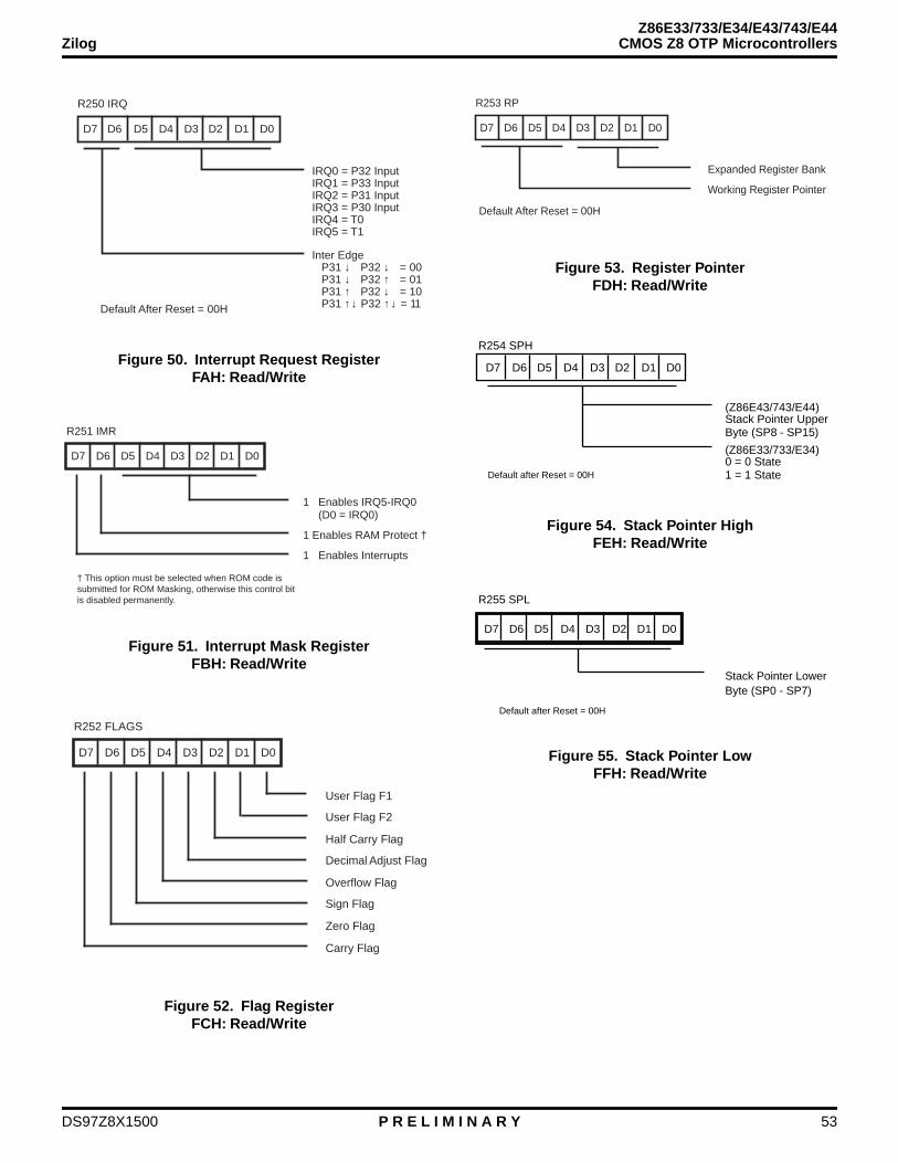
Z86E33/733/E34/E43/743/E44Zilog CMOS Z8 OTP Microcontrollers
1
Figure 50. Interrupt Request RegisterFAH: Read/Write
Figure 51. Interrupt Mask RegisterFBH: Read/Write
Figure 52. Flag RegisterFCH: Read/Write
D7 D6 D5 D4 D3 D2 D1 D0
R250 IRQ
Inter Edge P31 ↓ P32 ↓ = 00 P31 ↓ P32 ↑ = 01 P31 ↑ P32 ↓ = 10 P31 ↑↓ P32 ↑↓ = 11
IRQ0 = P32 InputIRQ1 = P33 InputIRQ2 = P31 InputIRQ3 = P30 InputIRQ4 = T0IRQ5 = T1
Default After Reset = 00H
D7 D6 D5 D4 D3 D2 D1 D0
1 Enables RAM Protect †
1 Enables IRQ5-IRQ0 (D0 = IRQ0)
1 Enables Interrupts
R251 IMR
† This option must be selected when ROM code is submitted for ROM Masking, otherwise this control bit is disabled permanently.
D7 D6 D5 D4 D3 D2 D1 D0
R252 FLAGS
User Flag F1
User Flag F2
Half Carry Flag
Decimal Adjust Flag
Overflow Flag
Sign Flag
Zero Flag
Carry Flag
Figure 53. Register PointerFDH: Read/Write
Figure 54. Stack Pointer HighFEH: Read/Write
Figure 55. Stack Pointer LowFFH: Read/Write
D7 D6 D5 D4 D3 D2 D1 D0
R253 RP
Expanded Register Bank
Working Register Pointer
Default After Reset = 00H
D7 D6 D5 D4 D3 D2 D1 D0
(Z86E43/743/E44)Stack Pointer UpperByte (SP8 - SP15)
R254 SPH
(Z86E33/733/E34)0 = 0 State1 = 1 StateDefault after Reset = 00H
D7 D6 D5 D4 D3 D2 D1 D0
Stack Pointer LowerByte (SP0 - SP7)
R255 SPL
Default after Reset = 00H
DS97Z8X1500 P R E L I M I N A R Y 53

Z86E33/733/E34/E43/743/E44CMOS Z8 OTP Microcontrollers Zilog
PACKAGE INFORMATION
Figure 56. 40-Pin DIP Package Diagram
Figure 57. 44-Pin PLCC Package Diagram
54 P R E L I M I N A R Y DS97Z8X1500

Z86E33/733/E34/E43/743/E44Zilog CMOS Z8 OTP Microcontrollers
1
Figure 58. 44-Pin QFP Package Diagram
Figure 59. 28-Pin DIP Package Diagram
DS97Z8X1500 P R E L I M I N A R Y 55

Z86E33/733/E34/E43/743/E44CMOS Z8 OTP Microcontrollers Zilog
Figure 60. 28-Pin SOIC Package Diagram
Figure 61. 28-Pin PLCC Package Diagram
56 P R E L I M I N A R Y DS97Z8X1500
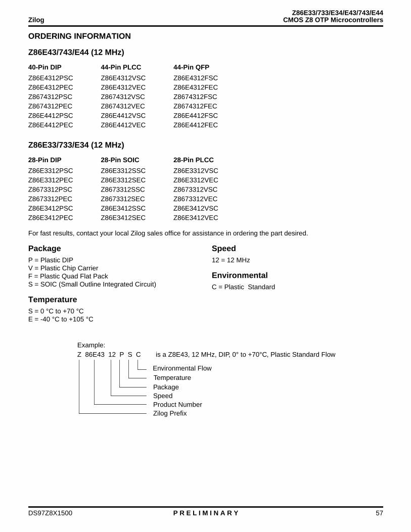
Z86E33/733/E34/E43/743/E44Zilog CMOS Z8 OTP Microcontrollers
1
ORDERING INFORMATION
Z86E43/743/E44 (12 MHz)
Z86E33/733/E34 (12 MHz)
For fast results, contact your local Zilog sales office for assistance in ordering the part desired.
PackageP = Plastic DIPV = Plastic Chip CarrierF = Plastic Quad Flat PackS = SOIC (Small Outline Integrated Circuit)
TemperatureS = 0 °C to +70 °CE = -40 °C to +105 °C
Speed12 = 12 MHz
EnvironmentalC = Plastic Standard
40-Pin DIP 44-Pin PLCC 44-Pin QFP
Z86E4312PSC Z86E4312VSC Z86E4312FSCZ86E4312PEC Z86E4312VEC Z86E4312FECZ8674312PSC Z8674312VSC Z8674312FSCZ8674312PEC Z8674312VEC Z8674312FECZ86E4412PSC Z86E4412VSC Z86E4412FSCZ86E4412PEC Z86E4412VEC Z86E4412FEC
28-Pin DIP 28-Pin SOIC 28-Pin PLCC
Z86E3312PSC Z86E3312SSC Z86E3312VSCZ86E3312PEC Z86E3312SEC Z86E3312VECZ8673312PSC Z8673312SSC Z8673312VSCZ8673312PEC Z8673312SEC Z8673312VECZ86E3412PSC Z86E3412SSC Z86E3412VSCZ86E3412PEC Z86E3412SEC Z86E3412VEC
Example:Z 86E43 12 P S C is a Z8E43, 12 MHz, DIP, 0° to +70°C, Plastic Standard Flow
Environmental FlowTemperaturePackageSpeedProduct NumberZilog Prefix
DS97Z8X1500 P R E L I M I N A R Y 57
Z86E33/733/E34/E43/743/E44CMOS Z8 OTP Microcontrollers Zilog
Pre-Characterization Product: The product represented by this CPS is newly introducedand Zilog has not completed the full characterization of theproduct. The CPS states what Zilog knows about thisproduct at this time, but additional features or non-conformance with some aspects of the CPS may be found,
either by Zilog or its customers in the course of furtherapplication and characterization work. In addition, Zilogcautions that delivery may be uncertain at times, due tostart-up yield issues.
© 1998 by Zilog, Inc. All rights reserved. No part of thisdocument may be copied or reproduced in any form or byany means without the prior written consent of Zilog, Inc.The information in this document is subject to changewithout notice. Devices sold by Zilog, Inc. are covered bywarranty and patent indemnification provisions appearingin Zilog, Inc. Terms and Conditions of Sale only.
ZILOG, INC. MAKES NO WARRANTY, EXPRESS,STATUTORY, IMPLIED OR BY DESCRIPTION,REGARDING THE INFORMATION SET FORTH HEREINOR REGARDING THE FREEDOM OF THE DESCRIBEDDEVICES FROM INTELLECTUAL PROPERTYINFRINGEMENT. ZILOG, INC. MAKES NO WARRANTYOF MERCHANTABILITY OR FITNESS FOR ANYPURPOSE.
Zilog, Inc. shall not be responsible for any errors that mayappear in this document. Zilog, Inc. makes no commitment
to update or keep current the information contained in thisdocument.
Zilog’s products are not authorized for use as criticalcomponents in life support devices or systems unless aspecific written agreement pertaining to such intended useis executed between the customer and Zilog prior to use.Life support devices or systems are those which areintended for surgical implantation into the body, or whichsustains life whose failure to perform, when properly usedin accordance with instructions for use provided in thelabeling, can be reasonably expected to result insignificant injury to the user.
Zilog, Inc. 210 East Hacienda Ave.Campbell, CA 95008-6600Telephone (408) 370-8000FAX 408 370-8056Internet: http://www.zilog.com
58 P R E L I M I N A R Y DS97Z8X1500