dynamic reconfiguration of 3d photonic networks-on-chip ... · photonic networks-on-chip for...
TRANSCRIPT
Dynamic Reconfiguration of 3D Photonic Networks-on-Chip for Maximizing Performance and Improving Fault Tolerance
Randy MorrisϮ, Avinash KodiϮ and Ahmed Louri ‡
School of Electrical Engineering and Computer Science, Ohio UniversityϮ
Department of Electrical and Computer Engineering, University of Arizona ‡
E-mail: [email protected], [email protected]
45th International Symposium on Microarchitecture (MICRO)
December 1 – December 5, 2012
Vancouver BC, Canada

Talk Outline
• Motivation & Background
• R-3PO: Architecture & Reconfiguration
• Performance Analysis
• Conclusions
2

Multicores & Network-on-Chips
• With increasing cores, communication-centric design paradigm is becoming important (Network-on-Chips)
• Energy for communication is increasing
• Delivered throughput is decreasing
3
Tilera-641 80-core Intel TeraFlops2 512-core FERMI (Nvidia)3
1http://www.tilera.com/products/processors/TILE64 2http://techresearch.intel.com/ProjectDetails.aspx?Id=151 3http://www.nvidia.com/object/fermi_architecture.html

0
25
50
75
100
125
150
175
200
225
250
Po
we
r (w
att
s)
Voltage
Tile Power: Intel Tera-Flops (65 nm)1
1. Y. Hoskote, “A 5-GHz Mesh Interconnect for A Teraflops Processor,”
IEEE Computer Society, 2007 pp. 51-61
Need to provide scalable bandwidth without sacrificing performance
Energy Discrepancy & Throughput • Energy discrepancy between
computation and global communication with technology scaling
• Reduced throughput due to aggressive voltage and clock scaling
4
1.33 Tflops
At 230 W
1 Tflops
at 97 W
=> Potential solutions:
Nanophotonics, 3D Stacking
0
0.2
0.4
0.6
0.8
1
1.2
45 32 22 14 10 7
Rel
ativ
e
Technology (nm)
Compute Energy
Interconnect Energy
On-die energy
Source: Shekar Borkar, Intel
Need to reduce global communication energy

Nanophotonics & Optical 3D Stacking
5
• Nanophotonics offers several advantages:
• Low energy (7.9 fJ/bit ) • Small Footprint (~2.5 µm) • High Bandwidth (~40 Gbps) • CMOS compatibility
• Optical 3D stacking offers several advantages:
• Shorter interconnect length • Higher bandwidth density • Optical vias create power-efficient inter-layer communication
1. L. Xu, W. Zhang, Q. Li, J. Chan, H. L. R. Lira, M. Lipson, K. Bergman, "40-Gb/s DPSK Data Transmission Through a Silicon Microring Switch," IEEE Photonics Technology Letters 24.
2. Sasikanth Manipatruni, Kyle Preston, Long Chen, and Michal Lipson, "Ultra-low voltage, ultra-small mode volume silicon microring modulator," Opt. Express 18, 18235-18242 (2010)
Layer 1
Layer 2
3. P. Koonath and B. Jalali, “Multilayer 3-d photonics in silicon,” Opt. Express, vol. 15, pp. 12 686–12 691, 2007.
4. A. Biberman, K. Preston, G. Hendry, N. Sherwood-Droz, J. Chan, J. S. Levy, M. Lipson, and K. Bergman, “Photonic network-on-chip architectures using multilayer deposited silicon
materials for high performance chip multiprocessors,” J. Emerg. Technol. Comput. Syst., vol. 7, pp. 1–25, July 2011.

6
Recent Work on Photonic NoC, among others
• However, there are several issues not addressed • 2D planar connections have waveguide crossings • Static network resource allocation • Lack of fault tolerance
• Shared-Bus [Cornell, MICRO’06]
• Circuit Switch [Columbia, NoCs’07]
• CORONA [HP/Wisconsin, ISCA’08]
• Processor-DRAM [MIT, Hot Int’08]
• Firefly [Northwestern, ISCA’09]
• Phastlane [Cornell, ISCA’09]
• Flexishare [Northwestern, HPCA’10]
• Oblivious Router [Cornell, ASPLOS’10]
• ATAC [MIT, PACT’10]
• MPNoC [Arizona, DAC’10]
• Free-Space Architecture [ISCA’10]
• Optical Proximity [Sun, ISCA’10] • PROPEL [Ohio, NoCs’10] • System Level Trimming [UC Davis,
HPCA’11] • Atomic Coherence [Wisconsin/HP, HPCA’11] • FeatherWeight [Northwestern/KAIST,
MICRO’11] • Resilient Microring Design [UCDavis,
MICRO’11] • Tolerating Process Variations [Pittsburgh,
ISCA’12]

Talk Outline
• Motivation & Background
• R-3PO: Architecture & Reconfiguration
• Performance Analysis
• Conclusions
7
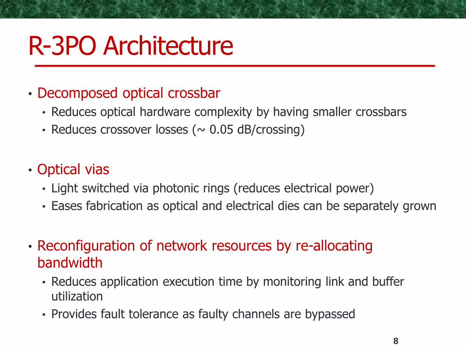
R-3PO Architecture
• Decomposed optical crossbar
• Reduces optical hardware complexity by having smaller crossbars
• Reduces crossover losses (~ 0.05 dB/crossing)
• Optical vias
• Light switched via photonic rings (reduces electrical power)
• Eases fabrication as optical and electrical dies can be separately grown
• Reconfiguration of network resources by re-allocating bandwidth
• Reduces application execution time by monitoring link and buffer utilization
• Provides fault tolerance as faulty channels are bypassed
8

Core + Cache + MC
Electro-Optic Transceivers
TSVs Electrical
Die
Optical Die
Heat Sink
External Laser
Electrical Contact
Optical Layer 0
Optical Layer 1
Optical Layer 2
Optical Layer 3
9
R-3PO Architecture (1/6)

Core + Cache + MC
R-3PO Architecture (1/6)
Electrical Die
Heat Sink
10
Core 0
Core 2
Core 1
Core 3
Sh
are
d L
2
L1
Ca
ch
e
L1
Ca
ch
e
L1
Ca
ch
e
L1
Ca
ch
e

Core + Cache + MC
Electro-Optic Transceivers
TSVs Electrical
Die
Heat Sink
External Laser
11
R-3PO Architecture (2/6)
Off-Chip Laser
Tx
Buffer Chain
TIA Limiting Amplifier
Driver for Electronics
Core A Core B
Tx Tx Tx Rx Rx Rx Rx
λ1 λ2 λ3 λ4 λ1 λ2 λ3 λ4
Photo- detector
Micro-ring resonator

Core + Cache + MC
Electro-Optic Transceivers
TSVs Electrical
Die
Heat Sink
External Laser
Optical Layer 0
12
Group 0 Group 1
Group 2 Group 3
R-3PO Architecture (3/6)

Core + Cache + MC
Electro-Optic Transceivers
TSVs Electrical
Die
Heat Sink
External Laser
Optical Layer 0
Optical Layer 1
13
Group 0 Group 1
Group 2 Group 3
R-3PO Architecture (4/6)

Core + Cache + MC
Electro-Optic Transceivers
TSVs Electrical
Die
Heat Sink
External Laser
Optical Layer 0
Optical Layer 1
Optical Layer 2
14
Group 2 Group 3
Group 0 Group 1
R-3PO Architecture (5/6)

Core + Cache + MC
Electro-Optic Transceivers
TSVs Electrical
Die
Optical Die
Heat Sink
External Laser
Electrical Contact
Optical Layer 0
Optical Layer 1
Optical Layer 2
Optical Layer 3
15
Group 0
Group 2
Group 1
Group 3
R-3PO Architecture (6/6)
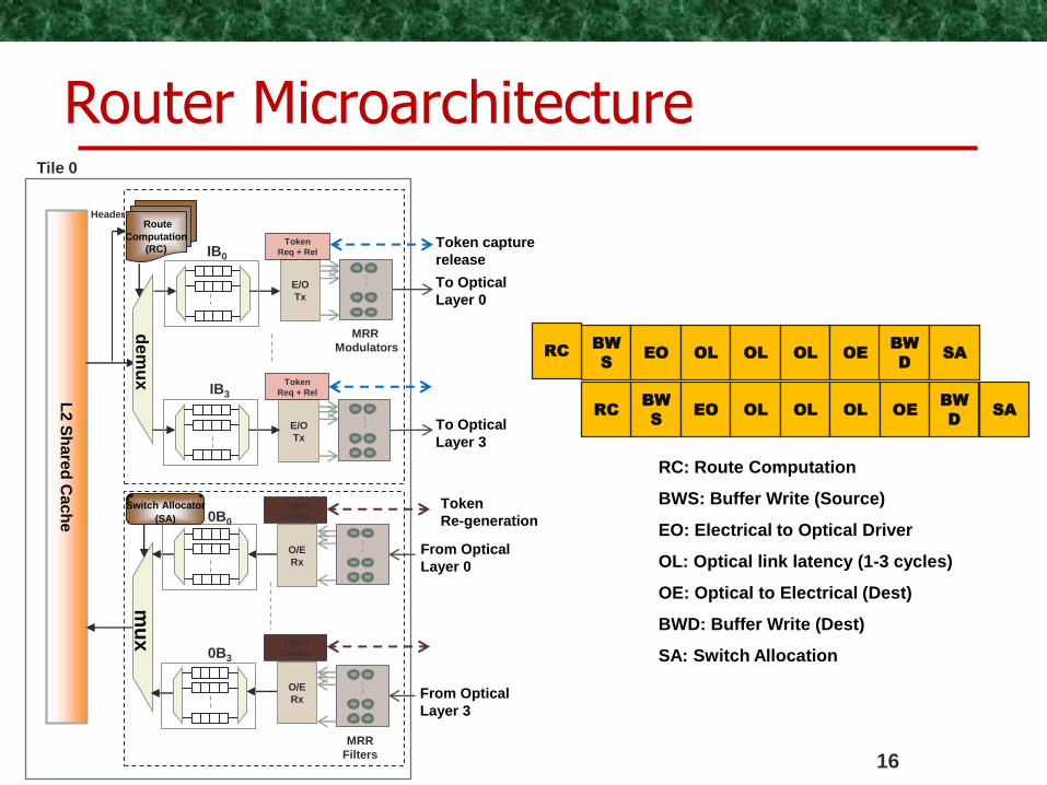
L2 S
hare
d C
ac
he
To Optical
Layer 0
To Optical
Layer 3
E/O
Tx
E/O
Tx
MRR
Modulators
Token
Req + Rel
de
mu
x
Route
Computation
(RC)
Header
Tile 0
IB0
IB3
Token
Req + Rel
Token capture
release
mu
x
O/E
Rx
O/E
Rx From Optical
Layer 3
From Optical
Layer 0
MRR
Filters
0B0
0B3
Token
Control
Token
Control
Token
Re-generation
Switch Allocator
(SA)
BW
S
RC EO OL OL OL OE BW
D SA
RC: Route Computation
BWS: Buffer Write (Source)
EO: Electrical to Optical Driver
OL: Optical link latency (1-3 cycles)
OE: Optical to Electrical (Dest)
BWD: Buffer Write (Dest)
SA: Switch Allocation
BW
S RC EO OL OL OL OE
BW
D SA
16
Router Microarchitecture

17
Group 2 Group 3
Group 0 Group 1 Source Layer 2
• Communication demand between Tile 0 and Tile 15 is high based on application
• If there are under-utilized links, then the bandwidth can be re-allocated to improve the performance
Static Communication

Destination
Group 0 Group 1
Group 2 Group 3
Layer 1 Group 0 Group 1
Group 2 Group 3
Source Layer 0
18
2x increase in bandwidth is obtained by routing half the data through two other nanophotonic channels
Network Reconfiguration
Switch point Combine point
Layer 0
Layer 1

19
Reconfiguration
• Reconfiguration in R-3PO takes place between the different layers as follows:
• R-3P0-L1: Reconfiguration between Layer0/Layer1 & Layer2/Layer3
• R-3P0-LA: Reconfiguration between adjacent layers
• R-3P0-L2: Reconfiguration between two adjacent layers
• R-3P0-L3: Reconfiguration between all layers
• Reconfiguration algorithm monitors network resources
• Link & Buffer utilization
• Accomplished with hardware counters & electrical circuitry

20
Step 1: Wait for Reconfiguration window, RW
t
Step 2: RCi sends a request packet to all local tiles requesting LinkUtil and BufferUtil for previous RWt-1
Step 3: Each hardware counter sends LinkUtil and BufferUtil statistics from the pervious RWt-1 to RCi
Step 4: RCi classifies the link statistic for each hardware counter as: If Linkutil = 0.0 Not-Utilized: Use β4 If Linkutil ≤ Lmin Under-Utilized: Use β3 If Linkutil ≥Lmin and Bufferutil < Bcon
Normal-Utilized: Use β2 If Bufferutil > Bcon Over-Utilized: Use β1 Step 5: Each RCi sends bandwidth available information to RCj, (i≠j). Step 6: If RCj can use any of the free links then notify RCi of their use, else RCj will forward to next RCj
Step 7a: RCi receives response back from RCj and activates corresponding microrings Step 7b: RCj notifies the tiles of additional bandwidth and RCi notifies RCj that the additional bandwidth is now available Step 8: Goto Step 1
Reconfiguration Algorithm

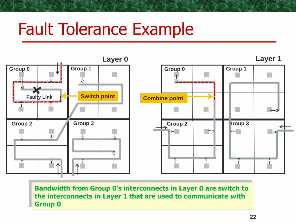
Fault Tolerance
• Channel faults cause communication breakdown isolating healthy cores due to transceiver failure (Eg., ring resonator failure due to thermal drift or process variation)
• As redundant channels are available in the decomposed crossbar, fault tolerance can be implemented
• Augment the reconfiguration algorithm to detect link faults
• When faults are detected, bandwidth from working links are shared with faulty links to communicate with the isolated core
• Fault tolerance techniques allow performance to degrade gracefully
21
22
Group 0 Group 1
Group 2 Group 3
Group 0 Group 1
Group 2 Group 3
Faulty Link
Layer 0 Layer 1
Switch point Combine point
Fault Tolerance Example
Bandwidth from Group 0’s interconnects in Layer 0 are switch to the interconnects in Layer 1 that are used to communicate with Group 0

Talk Outline
• Motivation & Background
• R-3PO: Architecture & Reconfiguration
• Performance Analysis
• Conclusions
23
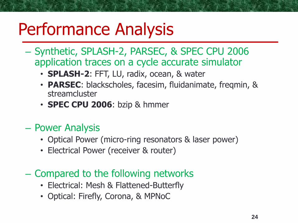
– Synthetic, SPLASH-2, PARSEC, & SPEC CPU 2006 application traces on a cycle accurate simulator
• SPLASH-2: FFT, LU, radix, ocean, & water
• PARSEC: blackscholes, facesim, fluidanimate, freqmin, & streamcluster
• SPEC CPU 2006: bzip & hmmer
– Power Analysis • Optical Power (micro-ring resonators & laser power)
• Electrical Power (receiver & router)
– Compared to the following networks • Electrical: Mesh & Flattened-Butterfly
• Optical: Firefly, Corona, & MPNoC
24
Performance Analysis

Off-Chip Laser
Tx
Buffer Chain
TIA Limiting Amplifier
Driver for Electronics
Core Core
Tx Tx Tx Rx Rx Rx Rx
λ1 λ2 λ3 λ4 λ1 λ2 λ3 λ4
Photo- detector
25
Laser Power
Pre-Driver and SERDES
Ring Heating & Ring modulation Ring
Heating
Optical Receiver Circuitry & DESERDES
Device Energy Device Energy
Ring Heating 2.6 fJ/bit Ring modulation 50 fJ/bit
Pre-Diver 19 fJ/bit SERDES 1.5 fJ/bit
DESERDES 1.5 fJ/bit Receiver Circuitry 66 fJ/bit
C. Batten, A. Joshi, J. Orcutt, A. Khilo, B. Moss, C. Holzwarth, M. Popović, H. Li, H. Smith, J. Hoyt, F. Kärtner, R. Ram, V. Stojanović, and K. Asanović. "Building Manycore Processor-to-DRAM Networks with Monolithic Silicon Photonics."16th Symposium on High-Performance Interconnects (HOTI-16), Aug. 2008.
Energy Evaluation

Parameter Value
L1/L2 coherence MOESI
L2 cache size/accos 4MB/16-way
L2 access latency (cycles) 4
L1 cache/accoc 64KB/4-way
L1 access latency (cycles) 2
Core Frequency (GHz) 5
Threads (core) 2
Issue Policy In-order
Memory Size (GB) 4
Memory latency (cycles) 160
R-3PO is compared to the following networks: Mesh, Flattened-Butterfly, Firefly, Corona, & MPNOC
26
System Simulation Parameters

0
0.5
1
1.5
2
2.5
Mesh FB Firefly Corona MPNOC R-3PO-L1 R-3PO-LA R-3PO-L2 R-3PO-L3
En
erg
y p
er
Bit
(p
J)
Ring modulation Ring heating Laser Back-end circuit Electrical link Router
27
R-3PO reduces energy consumption by 36%
Energy per bit (256 Cores): Uniform
36%

28
R-3PO shows an increase in performance of about 2.5x
Application Traffic (64 Cores)
0
0.5
1
1.5
2
2.5
3
3.5
blackscholes facesim fluidanimate freqmin streamcluster bzip hmmer
Sp
eed
-Up
Mesh Flattened-Butterfly Firefly Corona MPNOC R-3PO-L1 R-3PO-LA
29
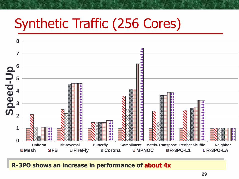
R-3PO shows an increase in performance of about 4x
Synthetic Traffic (256 Cores)
0
1
2
3
4
5
6
7
8
Uniform Bit-reversal Butterfly Compliment Matrix-Transpose Perfect Shuffle Neighbor
Sp
eed
-Up
Mesh FB FireFly Corona MPNOC R-3PO-L1 R-3PO-LA

30
Degrades performance when compared to R-3PO as follows: With 10% faults, performance loss is 3% With 25% faults, performance loss is 13% With 50% faults, performance loss is 35%
Fault Tolerance
0
0.2
0.4
0.6
0.8
1
1.2
blackscholes facesim fluidanimate freqmin streamcluster bzip hmmer
Pe
rfo
rma
nc
e D
eg
rad
ati
on
R-3PO-L1 R-3PO-L1(10%) R-3PO-L1(25%) R-3PO-L1(50%)

Talk Outline
• Motivation & Background
• R-3PO: Architecture & Reconfiguration
• Performance Analysis
• Conclusions
31

• R-3PO combines the benefits of nanophotonic and 3D stacking to reduce energy consumption while eliminating waveguide crossing
• We evaluate power-performance trade-off by analyzing the design space of implementing reconfiguration across multiple layers
• We apply our reconfiguration algorithm to bypass faulty channels by sharing bandwidth
• Our results indicate that energy/bit can be decreased by 23-36% for various real applications while improving application speedup by 2-4X
32
Conclusions

Thank You
Questions?

34
R-3PO shows an increase in performance of about 2.5x
Application Traffic (64 Cores/16λ)
0
0.5
1
1.5
2
2.5
3
blackscholes facesim fluidanimate freqmin streamcluster bzip hmmer
Sp
eed
-Up
Mesh Flattened-Butterfly Firefly Corona MPNOC R-3PO-L1 R-3PO-LA

Device Loss(dB) Device Loss(dB)
Coupler (Lc) 1 Filter drop (Lf) 1
Non-Linearity (Ln) 1 Bending (LB) 1
Photo-detector (Lp) 1 Waveguide Crossing (Lwc) 0.05
Modulator Insertion (Li)
1 Receiver (LRS) Sensitivity
-26 dBm (R-3PO)
Waveguide (per cm) (LW) 1.3 Splitter (Ls) 3
Laser Efficiently 30%
35
C. Batten, A. Joshi, J. Orcutt, A. Khilo, B. Moss, C. Holzwarth, M. Popović, H. Li, H. Smith, J. Hoyt, F. Kärtner, R. Ram, V. Stojanović, and K. Asanović.
"Building Manycore Processor-to-DRAM Networks with Monolithic Silicon Photonics."16th Symposium on High-Performance Interconnects (HOTI-16), Aug. 2008.
Power Analysis

020
4060
80100
120140
-30
-25
-20
-15
-60
-40
-20
0
20
40
60
80
100
120
Wavelengths
X: 64
Y: -26
Z: 6.1
Receiver Sensitivity (dBm)
Laser
Po
wer
(Watt
s)
Wavelengths Receiver
Sensitivity (dBm)
La
se
r P
ow
er
(W
att
s)
(a)
0.5
1
1.5
2
2.5
3
0
1
2
30
50
100
150
200
250
Waveguide Loss (dB)Ring Filter Loss (dB)
Laser
Po
wer
(Watt
s)
(b)
Waveguide Loss (dB) Ring Filter (dB)
La
se
r P
ow
er
(W
att
s)
Variation in Laser Power
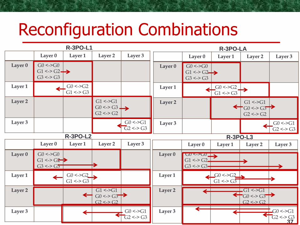
Layer 0 Layer 1 Layer 2 Layer 3
Layer 0 G0 <->G0 G1 <-> G2 G3 <-> G3
Layer 1 G0 <->G2 G1 <-> G3
Layer 2 G1 <->G1 G0 <-> G3 G2 <-> G2
Layer 3 G0 <->G1 G2 <-> G3
37
Layer 0 Layer 1 Layer 2 Layer 3
Layer 0 G0 <->G0 G1 <-> G2 G3 <-> G3
Layer 1 G0 <->G2 G1 <-> G3
Layer 2 G1 <->G1 G0 <-> G3 G2 <-> G2
Layer 3 G0 <->G1 G2 <-> G3
Layer 0 Layer 1 Layer 2 Layer 3
Layer 0 G0 <->G0 G1 <-> G2 G3 <-> G3
Layer 1 G0 <->G2 G1 <-> G3
Layer 2 G1 <->G1 G0 <-> G3 G2 <-> G2
Layer 3 G0 <->G1 G2 <-> G3
Layer 0 Layer 1 Layer 2 Layer 3
Layer 0 G0 <->G0 G1 <-> G2 G3 <-> G3
Layer 1 G0 <->G2 G1 <-> G3
Layer 2 G1 <->G1 G0 <-> G3 G2 <-> G2
Layer 3 G0 <->G1 G2 <-> G3
R-3PO-L1 R-3PO-LA
R-3PO-L2 R-3PO-L3
Reconfiguration Combinations