ds17885/ds17887 3 volt/5 volts real time...
TRANSCRIPT

1 of 36 081699
FEATURESIncorporates industry standard DS1287 PC clockplus enhanced features:§ Y2K-compliant§ +3 or +5-volt operation§ SMI recovery stack§ 64-bit silicon serial number§ Power control circuitry supports system
power-on from date/time alarm or keyclosure
§ 32 kHz output on power-up§ Crystal select bit allows RTC to operate with
6 pF or 12.5 pF crystal§ 114 bytes user NVRAM§ Auxiliary battery input§ 8K bytes additional NVRAM§ RAM clear input§ Century register§ Date alarm register§ Compatible with existing BIOS for original
DS1287 functions§ Available as chip (DS17885) or stand-alone
module with embedded battery and crystal(DS17887)
§ Timekeeping algorithm includes leap yearcompensation valid up to 2100
§ Optional industrial temperature range -40°Cto +85°C (DS17885 only)
PIN ASSIGNMENT
DS17885/DS178873 Volt/5 Volts Real Time Clock
www.dalsemi.com
PWR 123456789101112
23
DS17887 24-Pin EncapsulatedPackage
NC
AD1
AD3AD4AD5AD6AD7
GND
VCC
SQWVBAUX
RCLRNCIRQKSRDNCWRALECS
24
22212019181716151413
NC
AD0
AD2
PWR 123456789101112
23
DS17887 24-Pin DIPDS17887S 24-Pin SOIC
X2
AD1
AD3AD4AD5AD6AD7
GND
VCC
SQWVBAUX
RCLRVBAT
IRQKSRDGNDWRALE
CS
24
22212019181716151413
X1
AD0
AD2
IRQ 1 28 KS VBAT 2 27 RD RCLR 3 26 GND VBAUX 4 25 WR SQR 5 24 ALE VCC 6 23 CS VCC 7 22 GND PWR 8 21 GND X1 9 20 AD7 X2 10 19 AD6 NC 11 18 NC ADO 12 17 AD5 AD1 13 16 AD4 AD2 14 15 AD3
DS17885E 28-Pin TSOP

DS17885/DS17887
2 of 36
ORDERING INFORMATIONDS17885XX-X RTC Chip
DS17887-X RTC Module; 24-pin DIP
3 +3 Volt operating range5 +5 Volt operating range
PIN DESCRIPTIONX1 - Crystal InputX2 - Crystal OutputRCLR - RAM Clear InputAD0-AD7 - Mux’ed Address/Data BusPWR - Power-on Interrupt Output (open drain)KS - Kickstart InputCS - RTC Chip Select InputALE - RTC Address StrobeWR - RTC Write Data StrobeRD - RTC Read Data StrobeIRQ - Interrupt Request Output (open drain)SQW - Square Wave OutputVCC - +3 or +5 Volt Main SupplyGND - GroundVBAT - Battery + SupplyVBAUX - Auxiliary Battery SupplyNC - No Connect
DESCRIPTIONThe DS17885/DS17887 is a real time clock (RTC) designed as a successor to the industry standardDS1285, DS1385, DS1485, DS1585, and DS1685 PC real time clocks. This device provides the industrystandard DS1285 clock function with either +3.0 or +5.0-volt operation. The DS17885 also incorporates anumber of enhanced features, including a silicon serial number, power on/off control circuitry, 114 bytesof user NVSRAM plus 8 kbytes of additional NVRAM, and 32.768 kHz output for sustaining powermanagement activities.
The DS17885/DS17887 power control circuitry allows the system to be powered on via an externalstimulus, such as a keyboard or by a time and date (wake-up) alarm. The PWR output pin can betriggered by one or either of these events, and can be used to turn on an external power supply.
3 +3 Volt operating range5 +5 Volt operating range
blank commercial temp rangeN industrial temp range
blank 24-pin DIPE 28- pin TSOPS 24- pin SOIC

DS17885/DS17887
3 of 36
The PWR pin is under software control, so that when a task is complete the system power can then be shutdown.
The DS17885 is a clock/calendar chip with the features described above. An external crystal and batteryare the only components required to maintain time-of-day and memory status in the absence of power.The DS17887 incorporates the DS17885 chip, a 32.768 kHz crystal, and a lithium battery in a complete,self-contained timekeeping module. The entire unit is fully tested at Dallas Semiconductor such that aminimum of 10 years of timekeeping and data retention in the absence of VCC is guaranteed.
OPERATIONThe block diagram in Figure 1 shows the pin connections with the major internal functions of theDS17885/DS17887. The following paragraphs describe the function of each pin.
SIGNAL DESCRIPTIONSGND, VCC - DC power is provided to the device on these pins. VCC is the +3-volt or +5-volt input.
SQW (Square Wave Output) - The SQW pin will provide a 32 kHz square wave output, tREC, after apower-up condition has been detected. This condition sets the following bits enabling the 32 kHz output:DV1=1, and E32K=1. A square wave will be output on this pin if either SQWE=1 or E32K=1. IfE32K=1, then 32 kHz will be output regardless of the other control bits. If E32K=0, then the outputfrequency is dependent on the control bits in register A. The SQW pin can output a signal from one of 13taps provided by the 15 internal divider stages of the real time clock. The frequency of the SQW pin canbe changed by programming Register A as shown in Table 2. The SQW signal can be turned on and offusing the SQWE bit in register B or the E32K bit in extended register 4Bh. A 32 kHz SQW signal isoutput when the Enable 32 kHz (E32K) bit in extended register 4Bh is a logic 1, and VCC is above VPF. A32 kHz square wave is also available when VCC is less than VPF if E32K=1, ABE=1, and voltage isapplied to the VBAUX pin.
AD0-AD7 (Multiplexed Bi-directional Address/Data Bus) - Multiplexed buses save pins becauseaddress information and data information time-share the same signal paths. The addresses are presentduring the first portion of the bus cycle and the same pins and signal paths are used for data in the secondportion of the cycle. Address/data multiplexing does not slow the access time of the DS17885 since thebus change from address to data occurs during the internal RAM access time. Addresses must be validprior to the latter portion of ALE, at which time the DS17885/DS17887 latches the address. Valid writedata must be present and held stable during the latter portion of the WR pulse. In a read cycle theDS17885/DS17887 outputs 8 bits of data during the latter portion of the RD pulse. The read cycle isterminated and the bus returns to a high impedance state as RD transitions high. The address/data busalso serves as a bi-directional data path for the external extended RAM.
ALE (RTC Address Strobe Input; active high) - A pulse on the address strobe pin serves todemultiplex the bus. The falling edge of ALE causes the RTC address to be latched within theDS17885/DS17887.
RD (RTC Read Input; active low) - RD identifies the time period when the DS17885/DS17887 drivesthe bus with RTC read data. The RD signal is an enable signal for the output buffers of the clock.
WR (RTC Write Input; active low) - The WR signal is an active low signal. The WR signal defines thetime period during which data is written to the addressed register.

DS17885/DS17887
4 of 36
CS (RTC Chip Select Input; active low) - The Chip Select signal must be asserted low during a buscycle for DS17885/DS17887 to be accessed. CS must be kept in the active state during RD and WR
timing. Bus cycles which take place with ALE asserted but without asserting CS will latch addresses.However, no data transfer will occur.
IRQ (Interrupt Request Output; open drain, active low) - The IRQ pin is an active low output of theDS17885/DS17887 that can be tied to the interrupt input of a processor. The IRQ output remains low aslong as the status bit causing the interrupt is present and the corresponding interrupt-enable bit is set. Toclear the IRQ pin, the application software must clear all enabled flag bits contributing to IRQ ’s activestate.
When no interrupt conditions are present, the IRQ level is in the high impedance state. Multipleinterrupting devices can be connected to an IRQ bus. The IRQ pin is an open drain output and requires anexternal pullup resistor.
PWR (Power On Output; open drain, active low) - The PWR pin is intended for use as an on/offcontrol for the system power. With VCC voltage removed from the DS17885/DS17887, PWR may beautomatically activated from a Kickstart input via the KS pin or from a Wake-Up interrupt. Once thesystem is powered on, the state of PWR can be controlled via bits in the Dallas registers.
KS (Kickstart Input; active low) - When VCC is removed from the DS17885/DS17887, the system canbe powered on in response to an active low transition on the KS pin, as might be generated from a keyclosure. VBAUX must be present and Auxiliary Battery Enable bit (ABE) must be set to 1 if the Kickstartfunction is used, and the KS pin must be pulled up to the VBAUX supply. While VCC is applied, the KSpin can be used as an interrupt input.
RCLR (RAM Clear Input; active low) - If enabled by software, taking RCLR low will result in theclearing of the 114 bytes of user RAM. When enabled, RCLR can be activated whether or not VCC ispresent.
VBAUX - Auxiliary battery input required for kickstart and wake-up features. This input also supportsclock/ calendar and user RAM if VBAT is at lower voltage or is not present. A standard +3-volt lithiumcell or other energy source can be used. Battery voltage must be held between +2.5 and +3.7 volts forproper operation. If VBAUX is not going to be used it should be grounded and auxiliary battery enable bitbank 1, register 4BH, should=0.

DS17885/DS17887
5 of 36
DS17885/DS17887 BLOCK DIAGRAM Figure 1

DS17885/DS17887
6 of 36
DS17885 ONLYX1, X2 - Connections for a standard 32.768 kHz quartz crystal. For greatest accuracy, the DS17885 mustbe used with a crystal that has a specified load capacitance of either 6 pF or 12.5 pF. The Crystal Select(CS) bit in Extended Control Register 4B is used to select operation with a 6 pF or 12.5 pF crystal. Thecrystal is attached directly to the X1 and X2 pins. There is no need for external capacitors or resistors.Note: X1 and X2 are very high impedance nodes. It is recommended that they and the crystal be guard-ringed with ground and that high frequency signals be kept away from the crystal area.
For more information on crystal selection and crystal layout considerations, please consult ApplicationNote 58, “Crystal Considerations with Dallas Real Time Clocks.” The DS17885 can also be driven by anexternal 32.768 kHz oscillator. In this configuration, the X1 pin is connected to the external oscillatorsignal and the X2 pin is floated.
VBAT - Battery input for any standard 3-volt lithium cell or other energy source. Battery voltage must beheld between 2.5 and 3.7 volts for proper operation.
POWER-DOWN/POWER-UP CONSIDERATIONSThe real time clock function will continue to operate and all of the RAM, time, calendar, and alarmmemory locations remain nonvolatile regardless of the level of the VCC input. When VCC is applied to theDS17885/DS17887 and reaches a level of greater than VPF (power fail trip point), the device becomesaccessible after tREC, provided that the oscillator is running and the oscillator countdown chain is not inreset (see Register A). This time period allows the system to stabilize after power is applied.
The DS17885/DS17887 is available in either a 3-volt or a 5-volt device.
The 5-volt device is fully accessible and data can be written and read only when VCC is greater than 4.5volts. When VCC is below 4.5 volts, read and writes are inhibited. However, the timekeeping functioncontinues unaffected by the lower input voltage. As VCC falls below the greater of VBAT and VBAUX, theRAM and timekeeper are switched over to a lithium battery connected either to the VBAT pin or VBAUXpin.
The 3-volt device is fully accessible and data can be written or read only when VCC is greater than 2.7volts. When VCC falls below VPF, access to the device is inhibited. If VPF is less than VBAT and VBAUX ,the power supply is switched from VCC to the backup supply (the greater of VBAT and VBAUX) when VCCdrops below VPF. If VPF is greater than VBAT and VBAUX, the power supply is switched from VCC to thebackup supply when VCC drops below the larger of VBAT and VBAUX.
When VCC falls below VPF, the chip is write-protected. With the possible exception of the KS , PWR ,RCLR and SQW pins, all inputs are ignored and all outputs are in a high impedance state.
RTC ADDRESS MAPThe address map for the RTC registers of the DS17885/DS17887 is shown in Figure 2. The address mapconsists of the 14 clock/calendar registers. Ten registers contain the time, calendar, and alarm data, andfour bytes are used for control and status. All registers can be directly written or read except for thefollowing:1. Registers C and D are read-only.2. Bit-7 of Register A is read-only.3. The high order bit of the seconds byte is read-only.

DS17885/DS17887
7 of 36
DS17885 REAL TIME CLOCK ADDRESS MAP Figure 2
TIME, CALENDAR AND ALARM LOCATIONSThe time and calendar information is obtained by reading the appropriate register bytes shown in Table 1.The time, calendar, and alarm are set or initialized by writing the appropriate register bytes. The contentsof the time, calendar, and alarm registers can be either Binary or Binary-Coded Decimal (BCD) format.Table 1 shows the binary and BCD formats of the twelve time, calendar, and alarm locations that residein both bank 0 and in bank 1, plus the two extended registers that reside in bank 1 only (bank 0 and bank1 switching will be explained later in this text).
Before writing the internal time, calendar, and alarm registers, the SET bit in Register B should be writtento a logic 1 to prevent updates from occurring while access is being attempted. Also at this time, the dataformat (binary or BCD), should be set via the data mode bit (DM) of Register B. All time, calendar, andalarm registers must use the same data mode. The set bit in Register B should be cleared after the datamode bit has been written to allow the real time clock to update the time and calendar bytes.
Once initialized, the real time clock makes all updates in the selected mode. The data mode cannot bechanged without reinitializing the 10 data bytes. The 24/12 bit cannot be changed without reinitializingthe hour locations. When the 12-hour format is selected, the high order bit of the hours byte representsPM when it is a logic 1. The time, calendar, and alarm bytes are always accessible because they aredouble buffered. Once per second the 10 bytes are advanced by one second and checked for an alarmcondition. If a read of the time and calendar data occurs during an update, a problem exists whereseconds, minutes, hours, etc. may not correlate. The probability of reading incorrect time and calendardata is low. Several methods of avoiding any possible incorrect time and calendar reads are covered laterin this text.
The 4 alarm bytes can be used in two ways. First, when the alarm time is written in the appropriate hours,minutes, and seconds alarm locations, the alarm interrupt is initiated at the specified time each day if thealarm enable bit is high. The second use condition is to insert a “don’t care” state in one or more of the 4

DS17885/DS17887
8 of 36
alarm bytes. The “don’t care” code is any hexadecimal value from C0 to FF. The 2 most significant bitsof each byte set the “don’t care” condition when at logic 1. An alarm will be generated each hour whenthe “don’t care” bits are set in the hours byte. Similarly, an alarm is generated every minute with “don’tcare” codes in the hours and minute alarm bytes. The “don’t care” codes in all 3 alarm bytes create aninterrupt every second. The 3 alarm bytes may be used in conjunction with the date alarm as described inthe Wakeup/Kickstart section. The century counter will be discussed later in this text.
TIME, CALENDAR AND ALARM DATA MODES Table 1RANGEADDRESS
LOCATIONFUNCTION DECIMAL
RANGE BINARY DATA MODE BCD DATA MODE
OOH Seconds 0-59 00-3B 00-59
01H Seconds Alarm 0-59 00-3B 00-59
02H Minutes 0-59 00-3B 00-59
03H Minutes Alarm 0-59 00-3B 00-59
Hours 12-hr, Mode 1-12 01-0C AM, 8108C PM 01-12 AM, 81-92 PM04H
Hours 24-hr, Mode 0-23 00-17 00-23
Hours Alarm 12-hr, Mode 1-12 01-0C AM, 8108C PM 01-12 AM, 81-92 PM05H
Hours Alarm 24-hr, Mode 0-23 00-17 00-23
06H Days of the week Sunday=1 1-7 01-07 01-07
07H Date of Month 1-31 01-1F 01-31
08H Month 1-12 01-0C 01-12
09H Year 0-99 00-63 00-99
BANK 1, 48H Century 0-99 00-63 00-99
BANK 1, 49H Date Alarm 1-31 01-1F 01-31
CONTROL REGISTERSThe four control registers; A, B, C, and D reside in both bank 0 and bank 1. These registers are accessibleat all times, even during the update cycle.
NONVOLATILE RAM - RTCThe general purpose nonvolatile RAM bytes are not dedicated to any special function within theDS17885/DS17887. They can be used by the application program as nonvolatile memory and are fullyavailable during the update cycle.
The user RAM is divided into two separate memory banks. When the bank 0 is selected, the 14 real timeclock registers and 114 bytes of user RAM are accessible. When bank 1 is selected, an additional 8Kbytes of user RAM are accessible through the extended RAM address and data registers.
INTERRUPT CONTROLThe DS17885/DS17887 includes six separate, fully automatic sources of interrupt for a processor:1. Alarm interrupt2. Periodic interrupt3. Update-ended interrupt4. Wake-up interrupt5. Kickstart interrupt6. RAM clear interrupt
The conditions which generate each of these independent interrupts are described in greater detailelsewhere in this data sheet. This section describes the overall control of the interrupts.

DS17885/DS17887
9 of 36
The application software can select which interrupts, if any, are to be used. There are a total of 6 bitsincluding 3 bits in Register B and three bits in Extended Register B which enable the interrupts. Theextended register locations are described later. Writing a logic 1 to an interrupt enable bit permits thatinterrupt to be initiated when the event occurs. A logic 0 in the interrupt enable bit prohibits the IRQ pinfrom being asserted from that interrupt condition. If an interrupt flag is already set when an interrupt isenabled, IRQ will immediately be set at an active level, even though the event initiating the interruptcondition may have occurred much earlier. As a result, there are cases where the software should clearthese earlier generated interrupts before first enabling new interrupts.
When an interrupt event occurs, the relating flag bit is set to a logic 1 in Register C or in ExtendedRegister A. These flag bits are set regardless of the setting of the corresponding enable bit located eitherin Register B or in Extended Register B. The flag bits can be used in a polling mode without enabling thecorresponding enable bits.
However, care should be taken when using the flag bits of Register C as they are automatically cleared to0 immediately after they are read. Double latching is implemented on these bits so that bits which are setremain stable throughout the read cycle. All bits which were set are cleared when read and new interruptswhich are pending during the read cycle are held until after the cycle is completed. One, 2, or 3 bits canbe set when reading Register C. Each utilized flag bit should be examined when read to ensure that nointerrupts are lost.
The flag bits in Extended Register A are not automatically cleared following a read. Instead, each flag bitcan be cleared to 0 only by writing 0 to that bit.
When using the flag bits with fully enabled interrupts, the IRQ line will be driven low when an interruptflag bit is set and its corresponding enable bit is also set. IRQ will be held low as long as at least one ofthe six possible interrupt sources has it s flag and enable bits both set. The IRQF bit in Register C is a 1whenever the IRQ pin is being driven low as a result of one of the six possible active sources. Therefore,determination that the DS17885/DS17887 initiated an interrupt is accomplished by reading Register Cand finding IRQF=1. IRQF will remain set until all enabled interrupt flag bits are cleared to 0.
SQUARE WAVE OUTPUT SELECTIONThe SQW pin can be programmed to output a variety of frequencies divided down from the 32.768 kHzcrystal tied to X1 and X2. The square wave output is enabled and disabled via the SQWE bit in RegisterB or the E32K bit in extended register 4Bh. If the square wave is enabled (SQWE=1 or E32K=1), thenthe output frequency will be determined by the settings of the E32K bit in Extended Register 4Bh and bythe RS3-0 bits in Register A. If E32K=1, then a 32.768 kHz square wave will be output on the SQW pinregardless of the settings of RS3-0 and SQWE.
If E32K = 0, then the square wave output frequency is determined by the RS3-0 bits. These bits control a1-of-15 decoder which selects one of thirteen taps that divide the 32.768 kHz frequency. The RS3-0 bitsestablish the SQW output frequency as shown in Table 2. In addition, RS3-0 bits control the periodicinterrupt selection as described below.
If E32K=1, and the Auxiliary Battery Enable bit (ABE, bank 1; register 04BH) is enabled, and voltage isapplied to VBAUX then the 32 kHz square wave output signal will be output on the SQW pin in the absenceof VCC. This facility is provided to clock external power management circuitry. If any of the above

DS17885/DS17887
10 of 36
requirements are not met, no square wave output signal will be generated on the SQW pin in the absenceof VCC.
A pattern of 01X in the DV2, DV1, and DV0, bits respectively, will turn the oscillator on and enable thecountdown chain. Note that this is different than the DS1287, which required a pattern of 010 in thesebits. DV0 is now a “don’t care” because it is used for selection between register banks 0 and 1.
A pattern of 11X will turn the oscillator on, but the oscillator’s countdown chain will be held in reset, asit was in the DS1287. Any other bit combination for DV2 and DV1 will keep the oscillator off.
PERIODIC INTERRUPT SELECTIONThe periodic interrupt will cause the IRQ pin to go to an active state from once every 500 ms to onceevery 122 µms. This function is separate from the alarm interrupt which can be output from once persecond to once per day. The periodic interrupt rate is selected using the same RS3-0 bits in Register Awhich select the square wave frequency (see Table 2). Changing the bits affects both the square wavefrequency and the periodic interrupt output. However, each function has a separate enable bit in RegisterB. The SQWE and E32K bits control the square wave output. Similarly, the periodic interrupt is enabledby the PIE bit in Register B. The periodic interrupt can be used with software counters to measure inputs,create output intervals, or await the next needed software function.
UPDATE CYCLEThe Serialized RTC executes an update cycle once per second regardless of the SET bit in Register B.When the SET bit in Register B is set to one, the user copy of the double buffered time, calendar, alarmand elapsed time byte is frozen and will not update as the time increments. However, the time countdownchain continues to update the internal copy of the buffer. This feature allows the time to maintainaccuracy independent of reading or writing the time, calendar, and alarm buffers and also guarantees thattime and calendar information is consistent. The update cycle also compares each alarm byte with thecorresponding time byte and issues an alarm if a match or if a “don’t care” code is present in all alarmlocations.
There are three methods that can handle access of the real time clock that avoid any possibility ofaccessing inconsistent time and calendar data. The first method uses the update-ended interrupt. Ifenabled, an interrupt occurs after every up date cycle that indicates that over 999 ms are available to readvalid time and date information. If this interrupt is used, the IRQF bit in Register C should be clearedbefore leaving the interrupt routine.
A second method uses the update-in-progress bit (UIP) in Register A to determine if the update cycle is inprogress. The UIP bit will pulse once per second. After the UIP bit goes high, the update transfer occurs244 µs later. If a low is read on the UIP bit, the user has at least 244 µs before the time/calendar data willbe changed. Therefore, the user should avoid interrupt service routines that would cause the time neededto read valid time/calendar data to exceed 244 µs.

DS17885/DS17887
11 of 36
PERIODIC INTERRUPT RATE AND SQUARE WAVE OUTPUT FREQUENCYTable 2
EXT. REG. B SELECT BITS REGISTER A
E32K RS3 RS2 RS1 RS0
tPI PERIODIC INTERRUPTRATE
SQW OUTPUTFREQUENCY
0 0 0 0 0 None None
0 0 0 0 1 3.90625 ms 256 Hz
0 0 0 1 0 7.8125 ms 128 Hz
0 0 0 1 1 122.070 µs 8.192 kHz
0 0 1 0 0 244.141 µs 4.096 kHz
0 0 1 0 1 488.281 µs 2.048 kHz
0 0 1 1 0 976.5625 µs 1.024 kHz
0 0 1 1 1 1.953125 ms 512 Hz
0 1 0 0 0 3.90625 ms 256 Hz
0 1 0 0 1 7.8125 ms 128 Hz
0 1 0 1 0 15.625 ms 64 Hz
0 1 0 1 1 31.25 ms 32 Hz
0 1 1 0 0 62.5 ms 16 Hz
0 1 1 0 1 125 ms 8 Hz
0 1 1 1 0 250 ms 4 Hz
0 1 1 1 1 500 ms 2 Hz
1 X X X X * 32.768 kHz*RS3-RS0 determine periodic interrupt rates as listed for E32K=0.
The third method uses a periodic interrupt to determine if an update cycle is in progress. The UIP bit inRegister A is set high between the setting of the PF bit in Register C (see Figure 3). Periodic interruptsthat occur at a rate of greater than tBUC allow valid time and date information to be reached at eachoccurrence of the periodic interrupt. The reads should be complete within (tPI/ 2+tBUC) to ensure that datais not read during the update cycle.
UPDATE-ENDED AND PERIODIC INTERRUPT RELATIONSHIP Figure 3

DS17885/DS17887
12 of 36
REGISTER AMSB LSB
BIT 7 BIT 6 BIT 5 BIT 4 BIT 3 BIT 2 BIT 1 BIT 0UIP DV2 DV1 DV0 RS3 RS2 RS1 RS0
UIP - The Update In Progress (UIP) bit is a status flag that can be monitored. When the UIP bit is a 1, theupdate transfer will soon occur. When UIP is a 0, the update transfer will not occur for at least 244 µs.The time, calendar, and alarm information in RAM is fully available for access when the UIP bit is zero.The UIP bit is read-only. Writing the SET bit in Register B to a one inhibits any update transfer andclears the UIP status bit.
DV2, DV1, DV0 - These bits are defined as follows:DV2 = Countdown Chain
1 - resets countdown chain only if DV1=10 - countdown chain enabled
DV1 = Oscillator Enable0 - oscillator off1 - oscillator on, VCC power-up state
DV0 = Bank Select0 - original bank1 - extended registers
A pattern of 01X is the only combination of bits that will turn the oscillator on and allow the RTC to keeptime. A pattern of 11X will enable the oscillator but holds the countdown chain in reset. The next updatewill occur at 500 ms after a pattern of 01X is written to DV2, DV1, and DV0.
RS3, RS2, RS1, RS0 - These four rate-selection bits select one of the 13 taps on the 15-stage divider ordisable the divider output. The tap selected can be used to generate an output square wave (SQW pin)and/or a periodic interrupt. The user can do one of the following:
Enable the interrupt with the PIE bit;
Enable the SQW output pin with the SQWE or E32K bits;
Enable both at the same time and the same rate; or
Enable neither.
Table 2 lists the periodic interrupt rates and the square wave frequencies that can be chosen with the RSbits.
REGISTER BMSB LSB
BIT 7 BIT 6 BIT 5 BIT 4 BIT 3 BIT 2 BIT 1 BIT 0SET PIE AIE UIE SQWE DM 24/12 DSE

DS17885/DS17887
13 of 36
SET - When the SET bit is a 0, the update transfer functions normally by advancing the counts once persecond. When the SET bit is written to a 1, any update transfer is inhibited and the program can initializethe time and calendar bytes without an update occurring in the midst of initializing. Read cycles can beexecuted in a similar manner. SET is a read/write bit that is not modified by internal functions of theDS17885/DS17887.
PIE - The Periodic Interrupt Enable bit is a read/write bit which allows the Periodic Interrupt Flag (PF)bit in Register C to drive the IRQ pin low. When the PIE bit is set to 1, periodic interrupts are generatedby driving the IRQ pin low at a rate specified by the RS3-RS0 bits of Register A. A 0 in the PIE bitblocks the IRQ output from being driven by a periodic interrupt, but the Periodic Flag (PF) bit is still setat the periodic rate. PIE is not modified by any internal DS17885/DS17887 functions.
AIE - The Alarm Interrupt Enable (AIE) bit is a read/ write bit which, when set to a 1, permits the AlarmFlag (AF) bit in register C to assert IRQ . An alarm interrupt occurs for each second that the three timebytes equal the three alarm bytes including a “don’t care” alarm code of binary 11XXXXXX. When theAIE bit is set to 0, the AF bit does not initiate the IRQ signal. The internal functions of theDS17885/DS17887 do not affect the AIE bit.
UIE - The Update Ended Interrupt Enable (UIE) bit is a read/write that enables the Update End Flag (UF)bit in Register C to assert IRQ . The SET bit going high clears the UIE bit.
SQWE - When the Square Wave Enable (SQWE) bit is set to a 1 and E32K=0, a square wave signal atthe frequency set by the rate-selection bits RS3 through RS0 is driven out on the SQW pin. When theSQWE bit is set to 0 and E32K=0, the SQW pin is held low. SQWE is a read/write bit. SQWE is set to a1 when VCC is powered up.
DM - The Data Mode (DM) bit indicates whether time and calendar information is in binary or BCDformat. The DM bit is set by the program to the appropriate for-mat and can be read as required. This bitis not modified by internal functions. A 1 in DM signifies binary data while a 0 in DM specifies BinaryCoded Decimal (BCD) data.
24/12 - The 24/12 control bit establishes the format of the hours byte. A 1 indicates the 24-hour mode anda 0 indicates the 12-hour mode. This bit is read/write.
DSE - The Daylight Savings Enable (DSE) bit is a read/ write bit which enables two special updateswhen DSE is set to 1. On the first Sunday in April the time increments from 1:59:59 AM to 3:00:00 AM.On the last Sunday in October when the time first reaches 1:59:59 AM it changes to 1:00:00 AM. Thesespecial updates do not occur when the DSE bit is a 0. This bit is not affected by internal functions.
REGISTER CMSB LSB
BIT 7 BIT 6 BIT 5 BIT 4 BIT 3 BIT 2 BIT 1 BIT 0IRQF PF AF UF 0 0 0 0

DS17885/DS17887
14 of 36
IRQF - The Interrupt Request Flag (IRQF) bit is set to a 1 when one or more of the following are true:PF = PIE = 1 WF = WIE= 1AF = AIE = 1 KF = KSE= 1UF = UIE = 1 RF = RIE = 1
i.e., IRQF = (PF ? PIE) + (AF ? AIE) + (UF ? UIE) + (WF ? WIE) + (KF ? KSE) + (RF ? RIE)
Any time the IRQF bit is a 1, the IRQ pin is driven low. Flag bits PF, AF, and UF are cleared afterRegister C is read by the program.
PF - The Periodic Interrupt Flag (PF) is a read-only bit which is set to a 1 when an edge is detected on theselected tap of the divider chain. The RS3 through RS0 bits establish the periodic rate. PF is set to a 1independently of the state of the PIE bit. When both PF and PIE are 1s, the IRQ signal is active and willset the IRQF bit. The PF bit is cleared by a software read of Register C.
AF - A 1 in the Alarm Interrupt Flag (AF) bit indicates that the current time has matched the alarm time.If the AIE bit is also a 1, the IRQ pin will go low and a one will appear in the IRQF bit. A read ofRegister C will clear AF.
UF - The Update Ended Interrupt Flag (UF) bit is set after each update cycle. When the UIE bit is set to1, the one in UF causes the IRQF bit to be a 1, which will assert the IRQ pin. UF is cleared by readingRegister C.
BIT 3 THROUGH BIT 0 - These are unused bits of the status Register C. These bits always read 0 andcannot be written.
REGISTER DMSB LSB
BIT 7 BIT 6 BIT 5 BIT 4 BIT 3 BIT 2 BIT 1 BIT 0 VRT 0 0 0 0 0 0 0
VRT - The Valid RAM and Time (VRT) bit indicates the condition of the battery connected to the VBATpin or the battery connected to VBAUX, whichever is at a higher voltage. This bit is not writeable andshould always be a 1 when read. If a 0 is ever present, an exhausted lithium energy source is indicatedand both the contents of the RTC data and RAM data are questionable.
BIT 6 THROUGH BIT 0 - The remaining bits of Register D are not usable. They cannot be written and,when read, they will always read 0.
EXTENDED FUNCTIONSThe extended functions provided by the DS17885/DS17887 that are new to the RAMified RTC familyare accessed via a software controlled bank switching scheme, as illustrated in Figure 4. In bank 0, theclock/calendar registers and 50 bytes of user RAM are in the same locations as for the DS1287. As aresult, existing routines implemented within BIOS, DOS, or application software packages can gainaccess to the DS17885/DS17887 clock registers with no changes. Also in bank 0, an extra 64 bytes ofRAM are provided at addresses just above the original locations for a total of 114 directly addressablebytes of user RAM.

DS17885/DS17887
15 of 36
When bank 1 is selected, the clock/calendar registers and the original 50 bytes of user RAM still appearas bank 0. However, the Dallas registers which provide control and status for the extended functions willbe accessed in place of the additional 64 bytes of user RAM. The major extended functions controlled bythe Dallas registers are listed below:
1. 64-bit Silicon Serial Number
2. Century counter
3. Date Alarm
4. Auxiliary Battery Control/Status
5. Wake-Up
6. Kickstart
7. RAM Clear Control/Status
8. 8K bytes Extended RAM Access
The bank selection is controlled by the state of the DV0 bit in register A. To access bank 0 the DV0 bitshould be written to a 0. To access bank 1, DV0 should be written to a 1. Register locations designated asreserved in the bank 1 map are reserved for future use by Dallas Semiconductor. Bits in these locationscannot be written and will return a 0 if read.

DS17885/DS17887
16 of 36
DS17885/DS17887 EXTENDED REGISTER BANK DEFINITION Figure 4
SILICON SERIAL NUMBERA unique 64-bit lasered serial number is located in bank 1, registers 40h - 47h. This serial number isdivided into three parts. The first byte in register 40h contains a model number to identify the device typeand revision of the DS17885/DS17887. Registers 41h - 46h contain a unique binary number. Register 47h

DS17885/DS17887
17 of 36
contains a CRC byte used to validate the data in registers 40h - 46h. All 8 bytes of the serial number areread-only registers.
The DS17885/DS17887 is manufactured such that no two devices will contain an identical number inlocations 41h - 47h.
CENTURY COUNTERA register has been added in bank 1, location 48H, to keep track of centuries. The value is read in eitherbinary or BCD according to the setting of the DM bit.
RTC WRITE COUNTERAn 8-bit counter located in extended register bank 1, 5Eh, will count the number of times the RTC iswritten to. This counter will be incremented on the rising edge of the WR signal every time that the CSsignal qualifies it. This counter is a read-only register and will roll-over after 256 RTC write pulses. Thiscounter can be used to determine if and how many RTC writes have occurred since the last time thisregister was read.
8K X 8 EXTENDED RAMThe DS17885/DS17887 provides 8K x 8 of on-chip SRAM which is controlled as nonvolatile storagesustained from a lithium battery. On power-up, the RAM is taken out of write protect status by theinternal power OK signal (POK) generated from the write protect circuitry.
The on-chip 8K x 8 nonvolatile SRAM is accessed via the eight multiplexed address/data lines AD7 toAD0. Access to the SRAM is controlled by three on-chip latch registers. Two registers are used to holdthe SRAM address, and the other register is used to hold read/write data. The SRAM address space isfrom 00h to 01FFFh.
Access to the extended 8K x 8 RAM is controlled via three of the Dallas registers shown in Figure 4. TheDallas registers in bank 1 must first be selected by setting the DV0 bit in register A to a logic 1. The 12-bit address of the RAM location to be accessed must be loaded into the extended RAM address registerslocated at 50h and 51h. The least significant address byte should be written to location 50h, and the mostsignificant 5-bits (right-justified) should be loaded in location 51h. Data in the addressed location may beread by performing a read operation from location 53h, or written to by performing a write operation tolocation 53h. Data in any addressed location may be read or written repeatedly without changing theaddress in location 50h and 51h.
To read or write consecutive extended RAM locations, a burst mode feature can be enabled to incrementthe extended RAM address. To enable the burst mode feature, set the BME bit in the extended controlregister 4Ah, to a logic 1. With burst mode enabled, write the extended RAM starting address location toregisters 50h and 51h. Then read or write the extended RAM data from/to register 53h. The extendedRAM address locations are automatically incremented on the rising edge of RD or WR only whenregister 53h is being accessed. Refer to the Burst Mode Timing Waveform.
AUXILIARY BATTERYThe VBAUX input is provided to supply power from an auxiliary battery for the DS17885/DS17887kickstart, wake-up, and SQW output features in the absence of VCC. This power source must be availablein order to use these auxiliary features when no VCC is applied to the device.

DS17885/DS17887
18 of 36
The Auxiliary Battery Enable (ABE; bank 1, register 04BH) bit in extended control register B is used toturn on and off the auxiliary battery for the above functions in the absence of VCC. When set to a 1, VBAUX
battery power is enabled, and when cleared to 0, VBAUX battery power is disabled to these functions.
In the DS17885/DS17887, this auxiliary battery may be used as the primary backup power source formaintaining the clock/calendar, user RAM, and extended external RAM functions. This occurs if theVBAT pin is at a lower voltage than VBAUX. If the DS17885 is to be backed-up using a single battery withthe auxiliary features enabled, then VBAUX should be used and VBAT should be grounded. If VBAUX is notto be used, it should be grounded and ABE should be cleared to 0.
WAKE-UP/KICKSTARTThe DS17885/DS17887 incorporates a wake-up feature which can power the system on at apredetermined date through activation of the PWR output pin. In addition, the kickstart feature can allowthe system to be powered up in response to a low going transition on the KS pin, without operatingvoltage applied to the VCC pin. As a result, system power may be applied upon such events as a keyclosure, or modem ring detect signal. In order to use either the wake-up or the kickstart features, theDS17885/DS17887 must have an auxiliary battery connected to the VBAUX pin and the oscillator must berunning and the countdown chain must not be in reset (Register A DV2, DV1, DV0 = 01X). If DV2,DV1, and DV0 are not in this required state, the PWR pin will not be driven low in response to a kickstartor wakeup condition, while in battery-backed mode.
The wake-up feature is controlled through the Wake-up Interrupt Enable bit in extended control register B(WIE, bank 1, 04BH). Setting WIE to 1 enables the wake-up feature, clearing WIE to 0 disables it.Similarly, the kickstart feature is controlled through the Kickstart Interrupt Enable bit in extended controlregister B (KSE, bank 1, 04BH).
A wake-up sequence will occur as follows: When wake-up is enabled via WIE = 1 while the system ispowered down (no VCC voltage), the clock/calendar will monitor the current date for a match conditionwith the date alarm register (bank 1, register 049H). In conjunction with the date alarm register, the hours,minutes, and seconds alarm bytes in the clock/calendar register map (bank 0, registers 05H, 03H, and01H) are also monitored. As a result, a wake-up will occur at the date and time specified by the date,hours, minutes, and seconds alarm register values. This additional alarm will occur regardless of theprogramming of the AIE bit (bank 0, register B, 0BH). When the match condition occurs, the PWR pinwill automatically be driven low. This output can be used to turn on the main system power supply whichprovides VCC voltage to the DS17885/DS17887 as well as the other major components in the system.Also at this time, the Wake-Up flag (WF, bank 1, register 04AH) will be set, indicating that a wake-upcondition has occurred.
A kickstart sequence will occur when kickstarting is enabled via KSE = 1. While the system is powereddown, the KS input pin will be monitored for a low going transition of minimum pulse width tKSPW.When such a transition is detected, the PWR line will be pulled low, as it is for a wake-up condition. Alsoat this time, the Kickstart Flag (KF, bank 1, register 04AH) will be set, indicating that a kickstartcondition has occurred.
The timing associated with both the wake-up and kickstarting sequences is illustrated in the Wake-Up /Kickstart Timing Diagram in the Electrical Specifications section of this data sheet. The timing associatedwith these functions is divided into 5 intervals, labeled 1-5 on the diagram.
DS17885/DS17887
19 of 36
The occurrence of either a kickstart or wake-up condition will cause the PWR pin to be driven low, asdescribed above. During interval 1, if the supply voltage on the DS17885/DS17887 VCC pin rises abovethe 3-volt power fail level before the power on timeout period (tPOTO) expires, then PWR will remain atthe active low level. If VCC does not rise above the 3-volt power fail voltage in this time, then the PWR
output pin will be turned off and will return to its high impedance level. In this event, the IRQ pin willalso remain tri-stated. The interrupt flag bit (either WF or KF) associated with the attempted power onsequence will remain set until cleared by software during a subsequent system power on.
If VCC is applied within the timeout period, then the system power on sequence will continue as shown inintervals 2-5 in the timing diagram. During interval 2, PWR will remain active and IRQ will be driven toits active low level, indicating that either WF or KF was set in initiating the power on. In the diagram KSis assumed to be pulled up to the VBAUX supply. Also at this time, the PAB bit will be automaticallycleared to 0 in response to a successful power on. The PWR line will remain active as long as the PABremains cleared to 0.
At the beginning of interval 3, the system processor has begun code execution and clears the interruptcondition of WF and/or KF by writing 0s to both of these control bits. As long as no other interrupt withinthe DS17885/DS17887 is pending, the IRQ line will be taken inactive once these bits are reset. Executionof the application software may proceed. During this time, both the wake-up and kickstart functions maybe used to generate status and interrupts. WF will be set in response to a date, hours, minutes, andseconds match condition. KF will be set in response to a low going transition on KS . If the associatedinterrupt enable bit is set (WIE and/or KSE) then the IRQ line will driven active low in response toenabled event. In addition, the other possible interrupt sources within the DS17885/DS17887 may causeIRQ to be driven low. While system power is applied, the on chip logic will always attempt to drive thePWR pin active in response to the enabled kickstart or wake-up condition. This is true even if PWR waspreviously inactive as the result of power being applied by some means other than wake-up or kickstart.
The system may be powered down under software control by setting the PAB bit to a logic 1. This causesthe open-drain PWR pin to be placed in a high impedance state, as shown at the beginning of interval 4 inthe timing diagram. As VCC voltage decays, the IRQ output pin will be placed in a high impedance statewhen VCC goes below VPF. If the system is to be again powered on in response to a wake-up or kickstart,then the both the WF and KF flags should be cleared and WIE and/or KSE should be enabled prior tosetting the PAB bit.
During interval 5, the system is fully powered down. Battery backup of the clock calendar andnonvolatile RAM is in effect and IRQ is tri-stated, and monitoring of wake-up and kickstart takes place.If PRS=1, PWR stays active, otherwise if PRS=0 PWR is tri-stated.
RAM CLEARThe DS17885/DS17887 provides a RAM clear function for the 114 bytes of user RAM. When enabled,this function can be performed regardless of the condition of the VCC pin.
The RAM clear function is enabled or disabled via the RAM Clear Enable bit (RCE; bank 1, register04BH). When this bit is set to a logic 1, the 114 bytes of user RAM will be cleared (all bits set to 1)when an active low transition is sensed on the RCLR pin. This action will have no effect on either theclock/calendar settings or upon the contents of the extended RAM. The RAM clear Flag (RF, bank 1,
DS17885/DS17887
20 of 36
register 04AH) will be set when the RAM clear operation has been completed. If VCC is present at thetime of the RAM clear and RIE=1, the IRQ line will also be driven low upon completion. The interruptcondition can be cleared by writing a zero to the RF bit. The IRQ line will then return to its inactive highlevel provided there are no other pending interrupts. Once the RCLR pin is activated, all read/writeaccesses are locked out for a minimum recover time, specified as tREC in the Electrical Characteristicssection.
When RCE is cleared to 0, the RAM clear function is disabled. The state of the RCLR pin will have noeffect on the contents of the user RAM, and transitions on the RCLR pin have no effect on RF.
EXTENDED CONTROL REGISTERSTwo extended control registers are provided to supply controls and status information for the extendedfeatures offered by the DS17885/DS17887. These are designated as extended control registers A and Band are located in register bank 1, locations 04AH and 04BH, respectively. The functions of the bitswithin these registers are described as follows.
EXTENDED CONTROL REGISTER 4AMSB LSB
BIT 7 BIT 6 BIT 5 BIT 4 BIT 3 BIT 2 BIT 1 BIT 0 VRT2 INCR BME * PAB RF WF KF
VRT2 - This status bit gives the condition of the auxiliary battery. It is set to a logic 1 condition when theexternal lithium battery is connected to the VBAUX. If this bit is read as a logic 0, the external batteryshould be replaced.
INCR - Increment in Progress status bit. This bit is set to a 1 when an increment to the time/date registersis in progress and the alarm checks are being made. INCR will be set to a 1 at 122 µs before the updatecycle starts and will be cleared to 0 at the end of each update cycle.
BME - Burst Mode Enable. The burst mode enable bit allows the extended user RAM address registers toautomatically increment for consecutive reads and writes. When BME is set to a logic 1, the automaticincrementing will be enabled and when BME is set to a logic 0, the automatic incrementing will bedisabled.
PAB - Power Active Bar control bit. When this bit is 0, the PWR pin is in the active low state. When thisbit is 1, the PWR pin is in the high impedance state. This bit can be written to a logic 1 or 0 by the user. Ifeither WF AND WIE = 1 OR KF AND KSE = 1, the PAB bit will be cleared to 0.
RF - Ram Clear Flag. This bit will be set to a logic 1 when a high to low transition occurs on the V inputif RCE=1. The RF bit is cleared by writing it to a logic 0. This bit can also be written to a logic 1 toforce an interrupt condition.
WF – Wake-up Alarm Flag - This bit is set to 1 when a wake-up alarm condition occurs or when the userwrites it to a 1. WF is cleared by writing it to a 0.

DS17885/DS17887
21 of 36
KF - Kickstart Flag - This bit is set to a 1 when a kickstart condition occurs or when the user writes it to a1. This bit is cleared by writing it to a logic 0.
EXTENDED CONTROL REGISTER 4B
MSB LSBBIT 7 BIT 6 BIT 5 BIT 4 BIT 3 BIT 2 BIT 1 BIT 0 ABE E32K CS RCE PRS RIE WIE KSE
ABE - Auxiliary Battery Enable. This bit when written to a logic 1 will enable the VBAUX pin forextended functions.
E32K - Enable 32.768 kHz output. This bit when written to a logic 1 will enable the 32.768 kHzoscillator frequency to be output on the SQW pin. E32K is set to a one when VCC is powered up.
CS - Crystal Select Bit. When CS is set to a 0, the oscillator is configured for operation with a crystal thathas a 6 pF specified load capacitance. When CS=1, the oscillator is configured for a 12.5 pF crystal.
RCE - RAM Clear Enable bit. When set to a 1, this bit enables a low level on RCLR to clear all 114 bytesof user RAM. When RCE = 0, RCLR and the RAM clear function are disabled.
PRS - PAB Reset Select Bit. When set to a 0 the PWR pin will be set hi-Z when the DS17885 goes intopower fail. When set to a 1, the PWR pin will remain active upon entering power fail.
RIE - Ram Clear Interrupt Enable. When RIE is set to a 1, the IRQ pin will be driven low when a RAMclear function is completed.
WIE – Wake-up Alarm Interrupt Enable. When VCC voltage is absent and WIE is set to a 1, the PWR pinwill be driven active low when a wake-up condition occurs, causing the WF bit to be set to 1. When VCC
is then applied, the IRQ pin will also be driven low. If WIE is set while system power is applied, bothIRQ and PWR will be driven low in response to WF being set to 1. When WIE is cleared to a 0, the WFbit will have no effect on the PWR or IRQ pins.
KSE - Kickstart Interrupt Enable. When VCC voltage is absent and KSE is set to a 1, the PWR pin will bedriven active low when a kickstart condition occurs ( KS pulsed low), causing the KF bit to be set to 1.When VCC is then applied, the IRQ pin will also be driven low. If KSE is set to 1 while system power isapplied, both IRQ and PWR will be driven low in response to KF being set to 1. When KSE is cleared toa 0, the KF bit will have no effect on the PWR or IRQ pins.
* Reserved bits. These bits are reserved for future use by Dallas Semiconductor. They can be read andwritten, but have no effect on operation.

DS17885/DS17887
22 of 36
SYSTEM MAINTENANCE INTERRUPT (SMI) RECOVERY STACKAn SMI recovery register stack is located in the extended register bank, locations 4Eh and 4Fh. Thisregister stack, shown below, can be used by the BIOS to recover from an SMI occurring during an RTCread or write.
The RTC address is latched on the falling edge of the ALE signal. Each time an RTC address is latched,the register address stack is pushed. The stack is only four registers deep, holding the three previous RTCaddresses in addition to the current RTC address being accessed. The following waveform illustrates howthe BIOS could recover the RTC address when an SMI occurs.
1. The RTC address is latched.
2. An SMI is generated before an RTC read or write occurs.
3. RTC address 0Ah is latched and the address from "1" is pushed to the “RTC Address - 1” stacklocation. This step is necessary to change the bank select bit, DV0=1.
4. RTC address 4Eh is latched and the address from “1” is pushed to location 4Eh, “RTC Address -2” while 0Ah is pushed to the “RTC Address - 1” location. The data in this register, 4Eh, is theRTC address lost due to the SMI.

DS17885/DS17887
23 of 36
ABSOLUTE MAXIMUM RATINGS*Voltage on Any Pin Relative to Ground -0.3V to +7.0VOperating Temperature, Commercial temp 0° to 70°COperating Temperature, Industrial temp -40°C to +85°CStorage Temperature for DS17885 -55°C to +125°CStorage Temperature for DS17887 -40°C to +70°CSoldering Temperature 260°C for 10 seconds (See Note 13)
* This is a stress rating only and functional operation of the device at these or any other conditions abovethose indicated in the operation sections of this specification is not implied. Exposure to absolutemaximum rating conditions for extended periods of time may affect reliability.
RECOMMENDED DC OPERATING CONDITIONS (0°C to 70°C)PARAMETER SYMBOL MIN TYP MAX UNITS NOTES
Power Supply Voltage 5-VoltOperation
VCC 4.5 5.0 5.5 V 1
Power Supply Voltage 3-VoltOperation
VCC 2.7 3.0 3.3 V 1
Input Logic 1 VIH 2.3 VCC+0.3 V 1
Input Logic 0 VIL -0.3 0.6 V 1
Battery Voltage VBAT 2.5 3.7 V 1
Auxiliary Battery Voltage;VCC=5.0V
VBAUX 2.5 5.2 V 1
Auxiliary Battery Voltage;VCC=3.0V
VBAUX 2.5 3.7 V 1
DC ELECTRICAL CHARACTERISTICS (0°C to 70°C; VCC = 5.0V ± 10%)PARAMETER SYMBOL MIN TYP MAX UNITS NOTES
Average VCC Power SupplyCurrent
ICC1 25 50 mA 2,3
CMOS Standby Current( CS =VCC-0.2V)
ICC2 1 3 mA 2,3
Input Leakage Current(any input)
IIL -1 +1 µA
Output Leakage Current IOL -1 +1 µA 6
Output Logic 1 Voltage(IOUT = -1.0mA)
VOH 2.4 V

DS17885/DS17887
24 of 36
DC ELECTRICAL CHARACTERISTICS(cont’d)(0°C to 70°C; VCC = 5.0V ± 10%)Output Logic 0 Voltage(IOUT = +2.1mA)
VOL 0.4 V
Power Fail Trip Point VPF 4.25 4.37 4.5 V 4
Battery Switch Voltage VSW VBAT,VBAUX
V 9
Battery Leakage OSC ON IBAT1 0.50 0.7 µA 12
Battery Leakage OSC OFF IBAT2 0.050 0.4 µA 12
I/O Leakage ILO -1 +1 µA 5
PWR Output @ 0.4V IOLPWR 10.0 mA 1
IRQ Output @ 0.4V IOLIRQ 2.1 mA 1
DC ELECTRICAL CHARACTERISTICS (0°C to 70°C; VCC = 3.0V ± 10%)PARAMETER SYMBOL MIN TYP MAX UNITS NOTES
Average VCC Power SupplyCurrent
ICC1 15 30 mA 2,3
CMOS Standby Current( CS =VCC-0.2V)
ICC2 0.5 2 mA 2,3
Input Leakage Current(any input)
IIL -1 +1 µA
Output Leakage Current IOL -1 +1 µA 6
Output Logic 1 Voltage@ -0.4 mA
VOH 2.4 V
Output Logic 0 Voltage@ +0.8 mA
VOL 0.4 V
Power Fail Trip Point VPF 2.5 2.6 2.7 V 4
Battery Leakage OSC ON IBAT1 0.50 0.7 µA 12
Battery Leakage OSC OFF IBAT2 0.050 0.4 µA 12
I/O Leakage ILO -1 +1 µA 5
PWR Output @ 0.4V IOLPWR 4 mA 1
IRQ Output @ 0.4V IOLIRQ 0.8 mA 1

DS17885/DS17887
25 of 36
RTC AC TIMING CHARACTERISTICS (0°C to 70°C; VCC = 3.0V ± 10%)PARAMETER SYMBOL MIN TYP MAX UNITS NOTES
Cycle Time tCYC 360 DC ns
Pulse Width, RD / WR Low PWRWL 200 ns
Pulse Width, RD / WR High PWRWH 150 ns
Input Rise and Fall Time tR, tF 30 ns
Chip Select Setup TimeBefore WR or RD
tCS 20 ns
Chip Select Hold Time tCH 0 ns
Read Data Hold Time tDHR 10 90 ns
Write Data Hold Time tDHW 0 ns
Muxed Address Valid Time toALE Fall
tASL 40 ns
Muxed Address Hold Time toALE fall
tAHL 10 ns
RD or WR High Setup toALE Rise
tASD 30 ns
Pulse Width ALE High PWASH 40 ns
ALE Low Setup to RD
or WR Fall
tASED 30 ns
Output Data Delay Time fromRD
tDDR 20 200 ns 7
Data Setup Time tDSW 60 ns
IRQ Release from RD tIRD 2 µs
AC TEST CONDITIONSOutput Load: 50 pFInput Pulse Levels: 0-3.0VTiming Measurement Reference Levels
Input: 1.5VOutput: 1.5V
Input Pulse Rise and Fall Times: 5 ns

DS17885/DS17887
26 of 36
DS17885/DS17887 BUS TIMING FOR READ CYCLE TO RTC

DS17885/DS17887
27 of 36
RTC AC TIMING CHARACTERISTICS (0°C to 70°C; VCC = 5.0V ± 10%)PARAMETER SYMBOL MIN TYP MAX UNITS NOTES
Cycle Time tCYC 240 DC ns
Pulse Width, RD / WR Low PWRWL 120 ns
Pulse Width, RD / WR High PWRWH 80 ns
Input Rise and Fall Time tR, tF 30 nsChip Select Setup TimeBefore WR or RD
tCS 20 ns
Chip Select Hold Time tCH 0 nsRead Data Hold Time tDHR 10 50 nsWrite Data Hold Time tDHW 0 nsMuxed Address Valid Time toALE Fall
tASL 20 ns
Muxed Address Hold Time toALE fall
tAHL 10 ns
RD or WR High Setup toALE Rise
tASD 25 ns
Pulse Width ALE High PWASH 40 ns
ALE Low Setup to RD
or WR Fall
tASED 30 ns
Output Data Delay Time fromRD
tDDR 20 120 ns 7
Data Setup Time tDSW 30 ns
IRQ Release from RD tIRD 2 µs
DS17885/DS17887 BUS TIMING FOR WRITE CYCLE TO RTC AND RTCREGISTERS

DS17885/DS17887
28 of 36
POWER-UP CONDITION 3 VOLT DEVICE
POWER-DOWN CONDITION 3 VOLT DEVICE

DS17885/DS17887
29 of 36
POWER-UP CONDITION 5.0 VOLT DEVICE
POWER-DOWN CONDITION 5.0 VOLT DEVICE
DS17885/DS17887
30 of 36
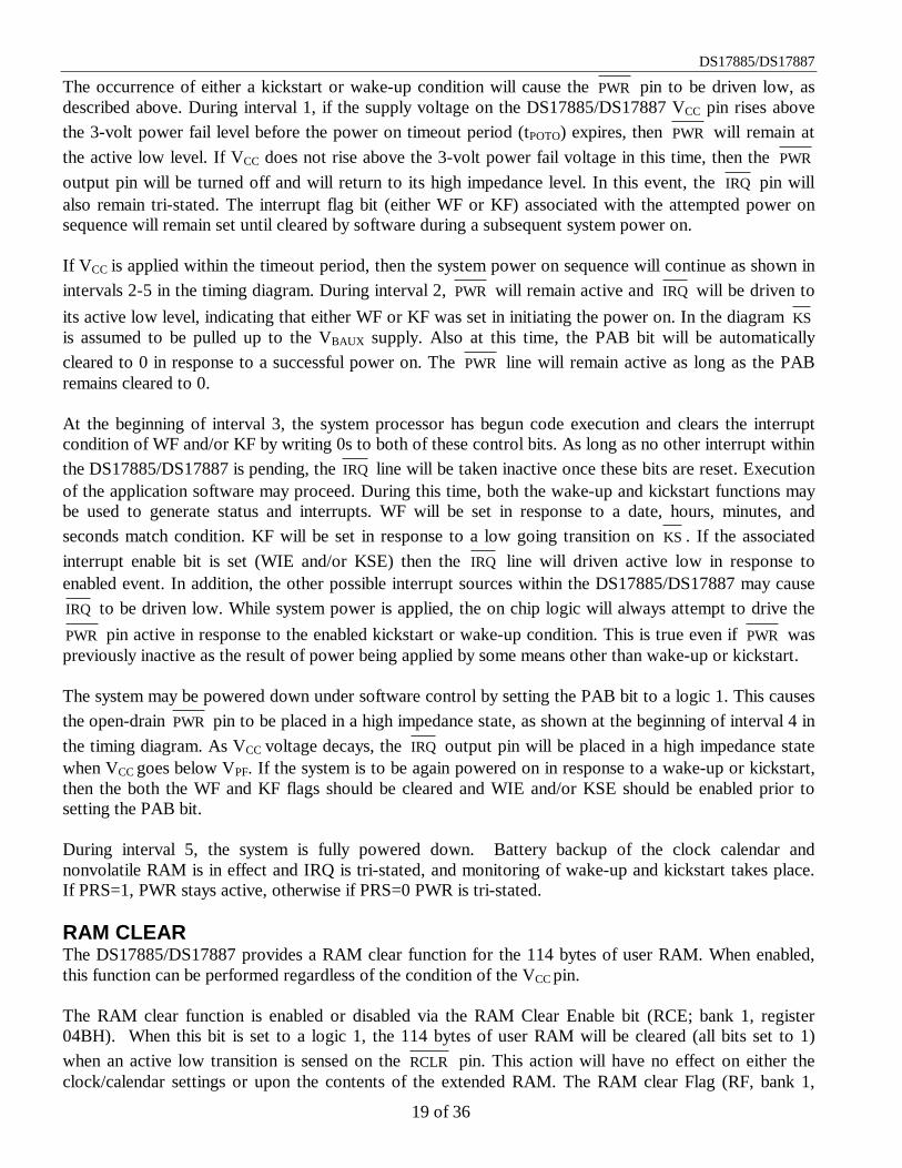
POWER-UP POWER-DOWN TIMING 5 VOLT DEVICE (tA=25°C)PARAMETER SYMBOL MIN TYP MAX UNITS NOTES
CS High to Power-fail tPF 0 ns
Recovery at Power-up tREC 150 msVCC Slew Rate Power-down tF
3.0=VCC= 4.5V300 µs
VCC Slew Rate Power-down tFB
4.0=VCC= 4.5V10 µs
VCC Slew Rate Power-up tR
4.5=VCC=4.0V0 µs
Expected Data Retention tDR 10 years 10,11
POWER-UP POWER-DOWN TIMING 3 VOLT DEVICE (tA=25°C)PARAMETER SYMBOL MIN TYP MAX UNITS NOTES
CS High to Power-fail tPF 0 ns
Recovery at Power-up tREC 150 msVCC Slew Rate Power-down tF
2.5=VCC= 3.0V300 µs
VCC Slew Rate Power-up tR
3.0=VCC=2.5V0 µs
Expected Data Retention tDR 10 years 10,11
Warning:Under no circumstances are negative undershoots, of any amplitude, allowed when device is in batteryback-up mode.
CAPACITANCE (tA=25°C)PARAMETER SYMBOL MIN TYP MAX UNITS NOTES
Input Capacitance CIN 12 PFOutput Capacitance COUT 12 pF
WAKE-UP/KICKSTART TIMING (tA=25°C)PARAMETER SYMBOL MIN TYP MAX UNITS NOTES
Kickstart Input Pulse width tKSPW 2 µsWake-up/Kickstart Power OnTimeout
tPOTO 2 seconds 8

DS17885/DS17887
31 of 36
WAKE-UP/KICKSTART TIMING
NOTE:Time intervals shown above are referenced in Wake-up/Kickstart section.* This condition can occur with the 3-volt device.

DS17885/DS17887
32 of 36
BURST MODE TIMING WAVEFORM
NOTES:1. All voltages are referenced to ground.
2. Typical values are at 25°C and nominal supplies.
3. Outputs are open.
4. Write protection trip point occurs during power fail prior to switchover from VCC to VBAT.
5. Applies to the AD0-AD7 pins, and the SQW pin when each is in a high impedance state.
6. The IRQ and PWR pins are open drain.
7. Measured with a load of 50 pF + 1 TTL gate.
8. Wakeup kickstart timeout generated only when the oscillator is enabled and the countdown chain isnot reset.
9. VSW is determined by the larger of VBAT and VBAUX.
10. The DS17887 will keep time to an accuracy of ±1 minute per month during data retention time for theperiod of tDR.
11. tDR is the amount of time that the internal battery can power the internal oscillator and internalregisters of the DS17887.
12. IBAT1 and IBAT2 are measured at VBAT = 3.5V.
13. Real Time Clock Modules can be successfully processed through conventional wave-solderingtechniques as long as temperature exposure to the lithium energy source contained within does notexceed +85°C. Post solder cleaning with water washing techniques is acceptable, provided thatultrasonic vibration is not used.

DS17885/DS17887
33 of 36
DS17885 24-PIN DIP
PKG 24-PINDIM MIN MAXA INMM
1.24531.62
1.27032.25
B INMM
0.53013.46
0.55013.97
C INMM
0.1403.56
0.1604.06
D INMM
0.60015.24
0.62515.88
E INMM
0.0150.380
0.0501.27
F INMM
0.1203.05
0.1453.68
G INMM
0.0902.29
0.1102.79
H INMM
0.62515.88
0.67517.15
J INMM
0.0080.20
0.0120.30
K INMM
0.0150.38
0.0220.56

DS17885/DS17887
34 of 36
DS17885 24-PIN SOIC
The chamfer on the body is optional. If it is not present, a terminal 1 identifier must be positioned so that½ or more of its area is contained in the hatched zone.
PKG 24-PINDIM MIN MAXA INMM
0.0942.38
0.1052.68
A1 INMM
0.0040.102
0.0120.30
A2 INMM
0.0892.26
0.0952.41
b INMM
0.0130.33
0.0200.51
C INMM
0.0090.229
0.0130.33
D INMM
0.59815.19
0.61215.54
e INMM
0.050 BSC1.27 BSC
E1 INMM
0.2907.37
0.3007.62
H INMM
0.39810.11
0.41610.57
L INMM
0.0160.40
0.0401.02
Θ 0° 8°

DS17885/DS17887
35 of 36
DS17885 28-PIN TSOP
PKG 28-PINDIM MIN MAX
A - 1.20A1 0.05 -A2 0.91 1.02b 0.18 0.27c 0.15 0.20D 13.20 13.60
D1 11.70 11.90E 7.90 8.10e 0.55 BSCL 0.30 0.70
L1 0.80 BSC56-G5003-000
DS17885/DS17887
36 of 36
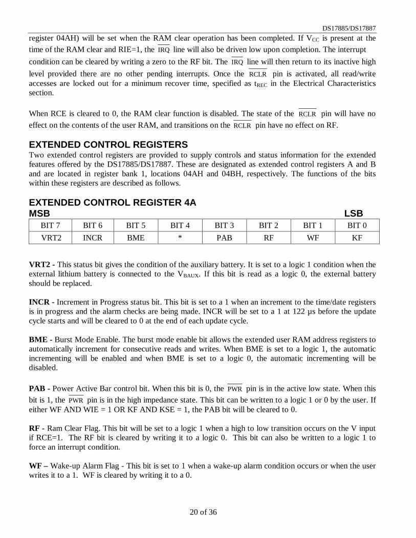
DS17887 REAL TIME CLOCK PLUS RAM
NOTE:Pins 2, 3, 16 and 20 are missing by design.
PKG 24-PINDIM MIN MAXA INMM
1.32033.53
1.33533.91
B INMM
0.72018.29
0.74018.80
C INMM
0.3458.76
0.3709.40
D INMM
0.1002.54
0.1303.30
E INMM
0.0150.38
0.0300.76
F INMM
0.1002.79
0.1403.56
G INMM
0.0902.29
0.1102.79
H INMM
0.59014.99
0.63016.00
J INMM
0.0080.20
0.0120.30
K INMM
0.0150.38
0.0210.53