drv8803-04-05-06 evm gui (rev. b)
TRANSCRIPT

DRV8803/04/05/06 Evaluation Module
User's Guide
Literature Number: SLVU574BSeptember 2011–Revised July 2019

2 SLVU574B–September 2011–Revised July 2019Submit Documentation Feedback
Copyright © 2011–2019, Texas Instruments Incorporated
Table of Contents
Contents
1 Trademarks ......................................................................................................................... 42 PCB.................................................................................................................................... 5
2.1 Test Points ................................................................................................................ 62.2 Connectors ................................................................................................................ 72.3 Jumpers/Resistors ....................................................................................................... 82.4 Motor Outputs............................................................................................................. 9
3 GUI Software Installation .................................................................................................... 103.1 System Requirements.................................................................................................. 103.2 Installation Procedure .................................................................................................. 10
4 The Windows Application .................................................................................................... 224.1 DRV8803 ................................................................................................................ 224.2 DRV8804 ................................................................................................................ 234.3 DRV8805 ................................................................................................................ 244.4 DRV8806 ................................................................................................................ 254.5 GUI Description/Functionality ......................................................................................... 264.6 DRV880x GPIO Control Signals ...................................................................................... 284.7 PWM Control ............................................................................................................ 314.8 Motor Control............................................................................................................ 324.9 Speed Control ........................................................................................................... 344.10 Acceleration Control .................................................................................................... 344.11 Diagnostic Output....................................................................................................... 354.12 Controlling the EVM Using External Signals ........................................................................ 35
5 Schematics........................................................................................................................ 35

www.ti.com
3SLVU574B–September 2011–Revised July 2019Submit Documentation Feedback
Copyright © 2011–2019, Texas Instruments Incorporated
List of Figures
List of Figures1 DRV8803/04/05/06 PCB .................................................................................................... 52 Test Points.................................................................................................................... 63 Power Connectors ........................................................................................................... 74 Jumpers/Resistors ........................................................................................................... 95 Motor Outputs............................................................................................................... 106 Setup_DRV8803/04/05/06_EVM.exe .................................................................................... 117 Installation Initialization .................................................................................................... 118 License Agreement ........................................................................................................ 129 NI License Agreement ..................................................................................................... 1210 Installation Directory Screen .............................................................................................. 1311 Component Selection ...................................................................................................... 1312 Configure Proxy ............................................................................................................ 1413 Ready to Install ............................................................................................................. 1414 Downloading RTE .......................................................................................................... 1515 LabVIEW RTE Self Extraction ............................................................................................ 1516 LabVIEW RTE Installation Initialization.................................................................................. 1617 Installation of LabVIEW RTE in Progress ............................................................................... 1618 FTDI Installation Initialization ............................................................................................. 1719 Driver Installation Wizard.................................................................................................. 1820 License Agreement for FTDI Driver...................................................................................... 1921 Driver Installation Completion ............................................................................................ 1922 Installation Complete....................................................................................................... 2023 Readme Window ........................................................................................................... 2024 DRV8803 Tab............................................................................................................... 2225 DRV8804 Tab............................................................................................................... 2326 DRV8805 Tab............................................................................................................... 2427 DRV8806 Tab............................................................................................................... 2528 Menu ......................................................................................................................... 2629 View .......................................................................................................................... 2630 Schematic Window......................................................................................................... 2731 Debug Window ............................................................................................................. 2732 Help Window................................................................................................................ 2833 About Window .............................................................................................................. 2834 GPIO Control Signals ...................................................................................................... 2935 SMx .......................................................................................................................... 3036 DRV8803 PWM Control ................................................................................................... 3137 Motor Control ............................................................................................................... 3238 DRV88003/04/05 Motor Control Windows .............................................................................. 3339 DRV88003/04/05 Speed Control Windows ............................................................................. 3440 DRV88003/04/05 Acceleration Control Windows ...................................................................... 3441 Acceleration Control ....................................................................................................... 35

www.ti.com
4 SLVU574B–September 2011–Revised July 2019Submit Documentation Feedback
Copyright © 2011–2019, Texas Instruments Incorporated
List of Figures
1 TrademarksAll trademarks are the property of their respective owners.
5SLVU574B–September 2011–Revised July 2019Submit Documentation Feedback
Copyright © 2011–2019, Texas Instruments Incorporated
DRV8803/04/05/06 Evaluation Module
User's GuideSLVU574B–September 2011–Revised July 2019
DRV8803/04/05/06 Evaluation Module
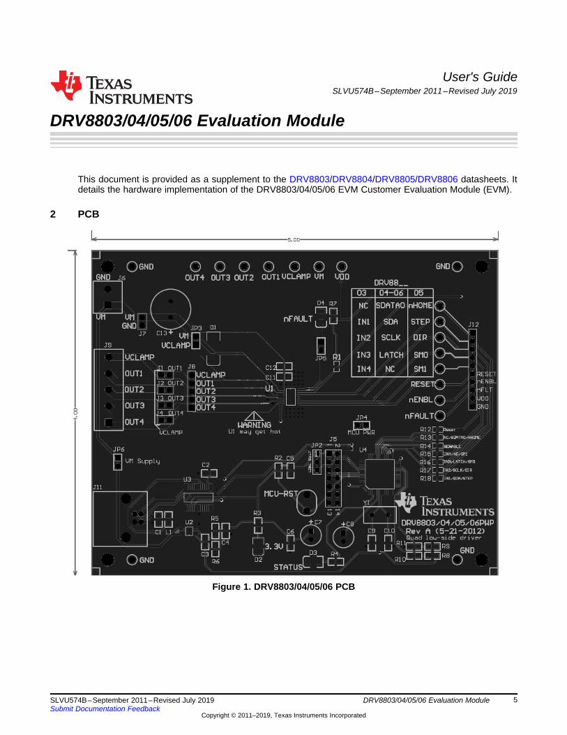
This document is provided as a supplement to the DRV8803/DRV8804/DRV8805/DRV8806 datasheets. Itdetails the hardware implementation of the DRV8803/04/05/06 EVM Customer Evaluation Module (EVM).
2 PCB
Figure 1. DRV8803/04/05/06 PCB

Test Points
PCB www.ti.com
6 SLVU574B–September 2011–Revised July 2019Submit Documentation Feedback
Copyright © 2011–2019, Texas Instruments Incorporated
DRV8803/04/05/06 Evaluation Module
2.1 Test PointsEvery pin on the DRV88xx device has been brought out to a test point, and labels on the silkscreenidentify each signal. These are Kelvin connections and are not meant to be used to drive high currents.These can be used as a sense line.
For those pins that change functionality depending on the respective device being used, a table isprovided with corresponding function name on its particular column.
Figure 2. Test Points

J6
J12
www.ti.com PCB
7SLVU574B–September 2011–Revised July 2019Submit Documentation Feedback
Copyright © 2011–2019, Texas Instruments Incorporated
DRV8803/04/05/06 Evaluation Module
2.2 Connectors
2.2.1 Power ConnectorsThe DRV88xx Customer EVM offers access to VM (Motor Voltage) power rail via a terminal block (J6) andheader pins (J7). A set of test clips at the top of the board in parallel with the terminal block allows for themonitoring of the input power rail. The polarity of the terminal connections are mentioned in the silkscreen.User must power the EVM using the correct polarity. User must apply VM according to datasheetrecommended parameters.
Figure 3. Power Connectors
PCB www.ti.com
8 SLVU574B–September 2011–Revised July 2019Submit Documentation Feedback
Copyright © 2011–2019, Texas Instruments Incorporated
DRV8803/04/05/06 Evaluation Module
2.2.2 Control SignalsThe header J12 brings out all the control signals of the IC. For the pins that have multiple functionalitydepending on the IC used, the various functions are labeled in a table. The correct functionality can beascertained from this table in the column corresponding to the IC being used. While the signals are beingdriven using the on-board MCU, these pins can be used to monitor the signals. However, the user canalso apply external signals using this header. In such a case, the on-board MCU should be powered off byde-populating the MCU_PWR jumper. This will ensure that the there is no conflict between the signalsapplied externally and the signals being forced by the on-board MCU. If only a few signals are beingdriven externally and the user wants to retain the on-board MCU for the remaining signals, thecorresponding resistors R12-R18 can be de-soldered to ensure that there is no conflict.
2.3 Jumpers/ResistorsnFault – If a jumper is applied at nFault (JP5), the LED (D4) will light in the case of a fault. Even if thejumper is not applied, the voltage of the nFault can be monitored across the two pin headers (JP5 orJP12).
LDO Supply – There is an LDO (TPS7A4001DGNT) on board that can regulate the VM voltage down to3.3 V. This voltage (VDD) is used to power the on board MCU (MSP430F2617) and is also used as thepull-up for the nFault pin. This voltage is used to light up the nFault LED. If a jumper is not applied to LDOsupply (JP6), the onboard MCU is no longer powered. If a jumper is not applied, the user must drive thepart using an external MCU by applying signals to the signal headers (J12), and the user must apply aVDD to implement the nFault LED function. If a jumper is applied the onboard MCU is powered on andcan be used to drive the part.
NOTE: If the user is applying an external VDD, please ensure that the jumpers JP6 (LDO Supply)and JP4 (MCU_PWR) are de-populated.
MCU_PWR - Applying a jumper at MCU PWR (JP4) enables the MSP430 and logic on the EVM. If thejumper is not applied, the user must implement an MCU or apply signals to the signal headers (J12). If thejumper is not applied nFault still receives VDD (3.3 V). If jumper at (JP4) is applied, MCU-RST works as amanual reset button for the MCU.
NOTE: Both JP4 and JP6 must be populated to enable the on board MCU and use theDRV8803/04/05 EVM software.
Resistors – R8, R9, R10, R11 are resistors used to identify which device is being implemented on theEVM (DRV8803, 04, 05 or 06). The MCU powers up based on these resistors. However, the GUI can beused to select the device on the EVM too. If the user changes the DRV8803 to another flavor of the IC(namely DRV8804/05/06) the appropriate tab in the GUI should be selected and ‘CONFIGURE DEVICE’should be selected.

www.ti.com PCB
9SLVU574B–September 2011–Revised July 2019Submit Documentation Feedback
Copyright © 2011–2019, Texas Instruments Incorporated
DRV8803/04/05/06 Evaluation Module
Figure 4. Jumpers/Resistors
2.4 Motor OutputsThere are two ways of connecting a bipolar stepper motor into the EVM: five pin header (J8), and fiveposition terminal block (J9). The optimal way to connect a DC motor is the two pin headers (J1/J2/J3/J4).Although feasible, we do not recommend the connection of any motor into the test clips as these areKelvin connections and are not rated for high current output. All pins are labeled on the silk-screen forclarity.

GUI Software Installation www.ti.com
10 SLVU574B–September 2011–Revised July 2019Submit Documentation Feedback
Copyright © 2011–2019, Texas Instruments Incorporated
DRV8803/04/05/06 Evaluation Module
Figure 5. Motor Outputs
3 GUI Software InstallationThe following section explains the location of files and the procedure for installing the software correctly.
NOTE: Ensure that no USB connections are made to the EVM until the installation is completed.The installer will also install LabVIEW RTE 2014 and FTDI Driver, along with the GUI.
3.1 System Requirements• Supported OS – Windows 7 (32 Bit, 64 Bit). The window text size should be Smaller-100% (Default)• Recommended RAM - 4 GB or higher• Recommended CPU Operating Speed – 3.3 GHz or higher
3.2 Installation ProcedureThe following procedure helps you install the DRV8803/04/05/06 EVM GUI1. Double click on the Setup_DRV8803/04/05/06_EVM.exe as in Figure 6.

www.ti.com GUI Software Installation
11SLVU574B–September 2011–Revised July 2019Submit Documentation Feedback
Copyright © 2011–2019, Texas Instruments Incorporated
DRV8803/04/05/06 Evaluation Module
Figure 6. Setup_DRV8803/04/05/06_EVM.exe
2. The screen in Figure 7 appears, indicating installer initialization. Click the Next button.
Figure 7. Installation Initialization
3. In the newly open installation pop-up window, click Next. The license agreement will be displayed.Please, read through it carefully and enable the "I Accept the Agreement" radio button and press Next.

GUI Software Installation www.ti.com
12 SLVU574B–September 2011–Revised July 2019Submit Documentation Feedback
Copyright © 2011–2019, Texas Instruments Incorporated
DRV8803/04/05/06 Evaluation Module
Figure 8. License Agreement
4. A screen as shown in Figure 9 appears, displaying the license agreement of National Instruments.Please read through the agreement carefully and enable the “I Accept the License Agreement” radiobutton and press the Next button.
Figure 9. NI License Agreement
5. Set the default directory for the GUI Installation and click Next.

www.ti.com GUI Software Installation
13SLVU574B–September 2011–Revised July 2019Submit Documentation Feedback
Copyright © 2011–2019, Texas Instruments Incorporated
DRV8803/04/05/06 Evaluation Module
Figure 10. Installation Directory Screen
NOTE: It is highly recommended to keep the default values as provided in the installer.
6. A screen as shown in Figure 11 appears. This screen is to select the components to install. Select theComponents to Install and Click Next to continue installation. The LabVIEW RTE component checksout if the LabVIEW RTE 2014 is already installed on the PC.
Figure 11. Component Selection
7. If LabVIEW RTE is selected as a component to install, a screen appears as shown in Figure 12.Configure the proxy settings as required. This screen is to download the LabVIEW RTE 2014 fromni.com, Click Next to continue the installation.

GUI Software Installation www.ti.com
14 SLVU574B–September 2011–Revised July 2019Submit Documentation Feedback
Copyright © 2011–2019, Texas Instruments Incorporated
DRV8803/04/05/06 Evaluation Module
Figure 12. Configure Proxy
8. A screen as shown in Figure 13 appears. Click Next to begin the installation.
Figure 13. Ready to Install
9. If the LabVIEW RTE 2014 is selected as a component to install, LabVIEW RTE downloads andperforms a silent mode installation.

www.ti.com GUI Software Installation
15SLVU574B–September 2011–Revised July 2019Submit Documentation Feedback
Copyright © 2011–2019, Texas Instruments Incorporated
DRV8803/04/05/06 Evaluation Module
Figure 14. Downloading RTE
10. Once the download completes, LabVIEW begins with the self-extraction as shown in Figure 15.
Figure 15. LabVIEW RTE Self Extraction
11. A screen appears as shown in Figure 16. It initializes the LabVIEW RTE Installation.

GUI Software Installation www.ti.com
16 SLVU574B–September 2011–Revised July 2019Submit Documentation Feedback
Copyright © 2011–2019, Texas Instruments Incorporated
DRV8803/04/05/06 Evaluation Module
Figure 16. LabVIEW RTE Installation Initialization
12. A display as shown in Figure 17 appears which indicates the progress of LabVIEW RTE installation.
Figure 17. Installation of LabVIEW RTE in Progress

www.ti.com GUI Software Installation
17SLVU574B–September 2011–Revised July 2019Submit Documentation Feedback
Copyright © 2011–2019, Texas Instruments Incorporated
DRV8803/04/05/06 Evaluation Module
13. Once the LabVIEW RTE 2014 is installed, Setup_DRV8803/04/05/06_EVM GUI component installs.14. After Setup_DRV8803/04/05/06_EVM Installation, FTDI Installation begins. A screen as shown in
Figure 18 appears, click Extract to proceed.
Figure 18. FTDI Installation Initialization
15. A screen as shown in Figure 19 appears, click Next to proceed.

GUI Software Installation www.ti.com
18 SLVU574B–September 2011–Revised July 2019Submit Documentation Feedback
Copyright © 2011–2019, Texas Instruments Incorporated
DRV8803/04/05/06 Evaluation Module
Figure 19. Driver Installation Wizard
16. The License Agreement appears on screen as shown in Figure 20.17. Read through the License Agreement carefully and enable the “I Accept this Agreement” radio button
and Click on Next.

www.ti.com GUI Software Installation
19SLVU574B–September 2011–Revised July 2019Submit Documentation Feedback
Copyright © 2011–2019, Texas Instruments Incorporated
DRV8803/04/05/06 Evaluation Module
Figure 20. License Agreement for FTDI Driver
18. Click Finish to complete the Driver Installation.
Figure 21. Driver Installation Completion

GUI Software Installation www.ti.com
20 SLVU574B–September 2011–Revised July 2019Submit Documentation Feedback
Copyright © 2011–2019, Texas Instruments Incorporated
DRV8803/04/05/06 Evaluation Module
19. Figure 22 appears denoting the completion of DRV8803/04/05/06 EVM GUI Installation. Click Finish.
Figure 22. Installation Complete
20. A Readme window as shown in Figure 23 appears displaying the link for LV 2014 RTE.
Figure 23. Readme Window

www.ti.com GUI Software Installation
21SLVU574B–September 2011–Revised July 2019Submit Documentation Feedback
Copyright © 2011–2019, Texas Instruments Incorporated
DRV8803/04/05/06 Evaluation Module
WARNINGThe DRV8803/04/05/06 EVM GUI requires the LabVIEW Run-TimeEngine 2014 to be installed before the GUI executes. Please notethe application is not compatible with other versions of LabVIEWRuntime Engine.
You can download National Instruments LabVIEW Run-Time Engine 2014from the below link:LabVIEW Run-Time Engine 2014
NOTE: DRV8803/04/05/06_EVM GUI executable has been built in LabVIEW 2014 (32-bit) version,and it expects the LabVIEW Run-Time Engine version to be LabVIEW Run-Time Engine (32-bit version).

The Windows Application www.ti.com
22 SLVU574B–September 2011–Revised July 2019Submit Documentation Feedback
Copyright © 2011–2019, Texas Instruments Incorporated
DRV8803/04/05/06 Evaluation Module
4 The Windows ApplicationThe DRV8803-04-05-06 EVM Windows application is the software counterpart for the DRV8803/04/05/06.It allows the PC to connect to the MSP430F2617 microcontroller through an USB interface chip. TheGraphical User Interface (GUI) has been designed to allow for all of the DRV88xx device’s functionality tobe tested without having to intervene with the hardware, except for the proper configuration of jumpers,when needed. Figure 24 shows the DRV8803-04-05-06 EVM High-Level Page.
The GUI has four High-Level Pages:• DRV8803• DRV8804• DRV8805• DRV8806
It contains frames with GPIO control for the DRV8803-04-05-06 control signals, stepper motor controlfor start/stop and speed, and Acceleration control.
4.1 DRV8803
Figure 24. DRV8803 Tab
The DRV8803 tab contains a diagram of the device which includes pin control and information aboutcontrol signals including: nENBL, RESET, IN1, IN2, IN3, and IN4. It also includes corresponding controlsto these pins (Enable Motor button, Reset button, and INx PWM and Duty Cycle number boxes).
Stepper control is implemented by controls in group boxes including: Motor Control, Speed Control, andAcceleration control.

www.ti.com The Windows Application
23SLVU574B–September 2011–Revised July 2019Submit Documentation Feedback
Copyright © 2011–2019, Texas Instruments Incorporated
DRV8803/04/05/06 Evaluation Module
4.2 DRV8804
Figure 25. DRV8804 Tab
The DRV8804 tab contains a diagram of the device which includes pin control and information aboutcontrol signals including: nENBL, and RESET. It also includes corresponding controls to these pins(Enable Motor button, and Reset button).
Stepper control is implemented by controls in group boxes including: Motor Control, Speed Control, andAcceleration control.
The DRV8804 tab also contains SPI package control in group box SPI Control.
The Windows Application www.ti.com
24 SLVU574B–September 2011–Revised July 2019Submit Documentation Feedback
Copyright © 2011–2019, Texas Instruments Incorporated
DRV8803/04/05/06 Evaluation Module
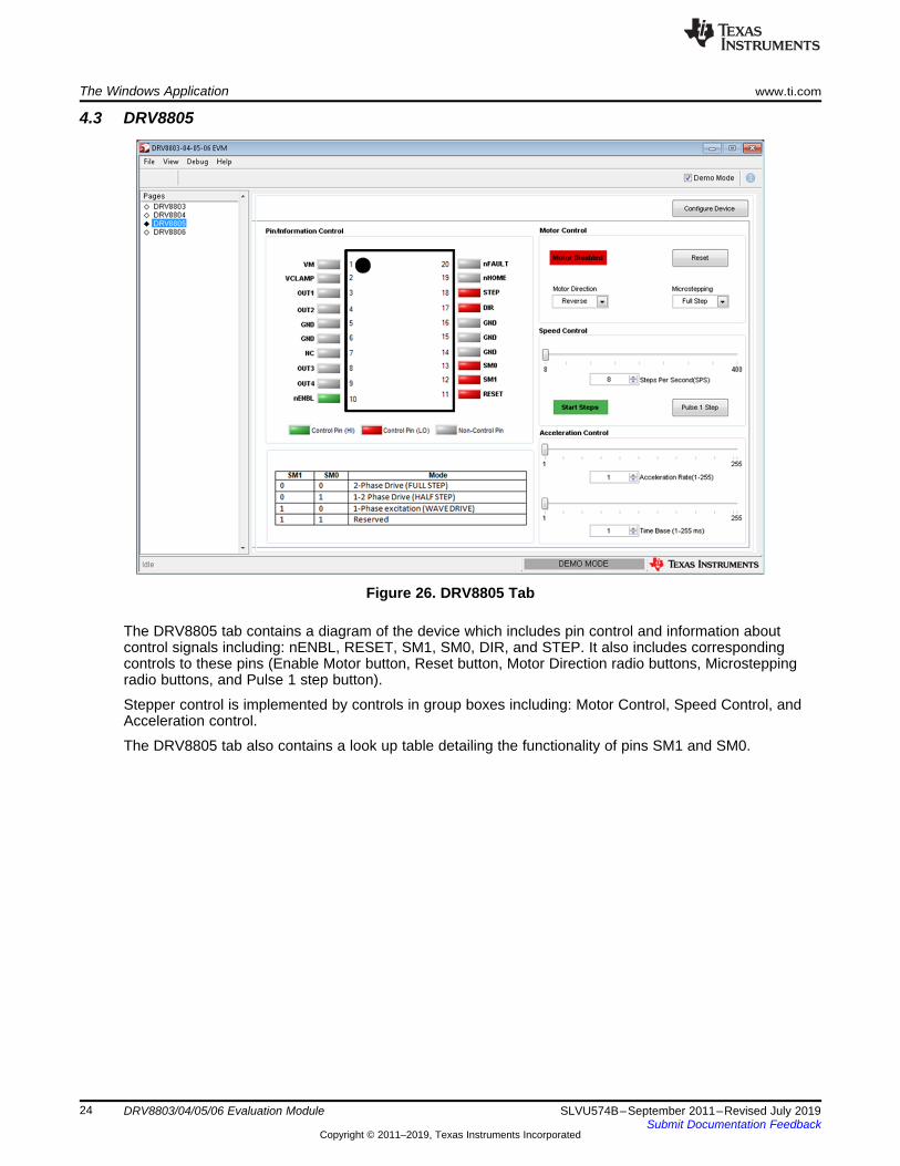
4.3 DRV8805
Figure 26. DRV8805 Tab
The DRV8805 tab contains a diagram of the device which includes pin control and information aboutcontrol signals including: nENBL, RESET, SM1, SM0, DIR, and STEP. It also includes correspondingcontrols to these pins (Enable Motor button, Reset button, Motor Direction radio buttons, Microsteppingradio buttons, and Pulse 1 step button).
Stepper control is implemented by controls in group boxes including: Motor Control, Speed Control, andAcceleration control.
The DRV8805 tab also contains a look up table detailing the functionality of pins SM1 and SM0.

www.ti.com The Windows Application
25SLVU574B–September 2011–Revised July 2019Submit Documentation Feedback
Copyright © 2011–2019, Texas Instruments Incorporated
DRV8803/04/05/06 Evaluation Module
4.4 DRV8806
Figure 27. DRV8806 Tab
The DRV8806 tab contains a diagram of the device which includes pin control and information aboutcontrol signals. Clicking on the nENBL and RESET will toggle the respective control signal state.
The DRV8806 tab also contains SPI packaging control in the SPI Control box. Since DRV8806 is basedaround a read back SPI which offers diagnostics information, said output is made available at the FaultDiagnostics group box.

The Windows Application www.ti.com
26 SLVU574B–September 2011–Revised July 2019Submit Documentation Feedback
Copyright © 2011–2019, Texas Instruments Incorporated
DRV8803/04/05/06 Evaluation Module
4.5 GUI Description/Functionality
4.5.1 The Menu Bar
Figure 28. Menu
The menu at the top of the application offers a series of quick options for how the COM port is to behave,and an option to view functional block diagrams of the respective chip. Please refer to the datasheet forthe most updated functional block diagrams.
File:Exit - Terminates the application.View:Schematic - which takes the user to a menu of different device schematics that are available forviewing.
Figure 29. View
This will take you to a window resembling the following:

www.ti.com The Windows Application
27SLVU574B–September 2011–Revised July 2019Submit Documentation Feedback
Copyright © 2011–2019, Texas Instruments Incorporated
DRV8803/04/05/06 Evaluation Module
Figure 30. Schematic Window
Debug:The Debug option can be used for the following operations.Debug - By selecting the Demo in the submenu, the GUI will run in simulation mode, and byunselecting it, the GUI will run in connected mode.Debug Log -
The Debug log option will enable to log all the activities of the user. If that is not selected, only thehigh-level operations will be logged.
Log to File -The log to file submenu is used to log the GUI activities to a log file that is specified.
Figure 31. Debug Window
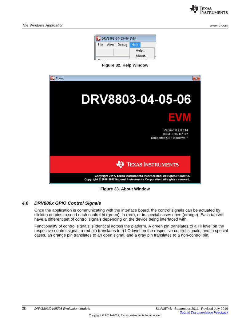
Help:Clicking the About in the Help Menu.About -
The About Page provides the details like the Name of the GUI, GUI version, Supported OS andCopyright Information.
The Windows Application www.ti.com
28 SLVU574B–September 2011–Revised July 2019Submit Documentation Feedback
Copyright © 2011–2019, Texas Instruments Incorporated
DRV8803/04/05/06 Evaluation Module
Figure 32. Help Window
Figure 33. About Window
4.6 DRV880x GPIO Control SignalsOnce the application is communicating with the interface board, the control signals can be actuated byclicking on pins to send each control hi (green), lo (red), or in special cases open (orange). Each tab willhave a different set of control signals depending on the device being interfaced with.
Functionality of control signals is identical across the platform. A green pin translates to a HI level on therespective control signal, a red pin translates to a LO level on the respective control signals, and in specialcases, an orange pin translates to an open signal, and a gray pin translates to a non-control pin.

Control Pin (Hi) Control Pin (LO) Non-control Pin Control Pin (Open)
1
2
3
4
5
6
7
8
20
19
18
17
16
15
14
13
nFAULT
NC
IN1
IN2
GND
GND
GND
IN3
VM
VCLAMP
OUT2
GND
GND
NC
OUT3
OUT1
9
10
12
11
IN4
RESET
OUT4
nENBL
1
2
3
4
5
6
7
8
20
19
18
17
16
15
14
13
nFAULT
SDATAO
SDATAIN
SCLK
GND
GND
GND
LATCH
VM
VCLAMP
OUT2
GND
GND
NC
OUT3
OUT1
9
10
12
11
NC
RESET
OUT4
nENBL
Control Pin (Hi) Control Pin (LO) Non-control Pin
1
2
3
4
5
6
7
8
20
19
18
17
16
15
14
13
nFAULT
nHOME
STEP
DIR
GND
GND
GND
SM0
VM
VCLAMP
OUT2
GND
GND
NC
OUT3
OUT1
9
10
12
11
SM1
RESET
OUT4
nENBL
Control Pin (Hi) Control Pin (LO) Non-control Pin
www.ti.com The Windows Application
29SLVU574B–September 2011–Revised July 2019Submit Documentation Feedback
Copyright © 2011–2019, Texas Instruments Incorporated
DRV8803/04/05/06 Evaluation Module
Figure 34. GPIO Control Signals
The Windows Application www.ti.com
30 SLVU574B–September 2011–Revised July 2019Submit Documentation Feedback
Copyright © 2011–2019, Texas Instruments Incorporated
DRV8803/04/05/06 Evaluation Module
nENBL – Control appears on all three devices. Toggling it LO (red) enables the chip, and toggling it HI(green) disables the chip. Automatically toggles in correspondence to the Enable Button on all three chips(See motor control).
Reset – Control appears on all three devices. Must be toggled LO (red) in order for the device to operate.If toggled HI (green) and then LO (red) it resets the chip. Automatically toggles in correspondence toReset Button (See motor control).
INx – Control appears on the DRV8803 device. Toggling HI (green) sets PWM of input X to a duty cycle of100%. Toggling LO (red) sets PWM of input X to a duty cycle of 0%. Automatically toggles incorrespondence to INx sliders and % duty cycle combo boxes (See PWM control). The pin will showorange if the user selects anything other than a 0% of 100% duty cycle. If user clicks pin to toggle fromorange the pin will go LO (red).
STEP – Control appears on the DRV8805 device. Toggling LO (red) and then HI (green) will enable abipolar stepper motor to step once. Toggles in correspondence to Pulse 1 Step button (See speedcontrol).
DIR – Control appears on the DRV8805 device. Toggling HI (green) will allow the motor to operate in theforward direction, while toggling LO (red) will allow the motor to operate in the reverse direction.Automatically toggles in correspondence to Motor Direction radio buttons (See Motor Control)
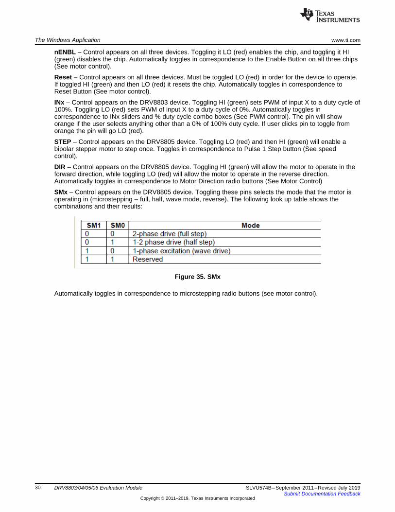
SMx – Control appears on the DRV8805 device. Toggling these pins selects the mode that the motor isoperating in (microstepping – full, half, wave mode, reverse). The following look up table shows thecombinations and their results:
Figure 35. SMx
Automatically toggles in correspondence to microstepping radio buttons (see motor control).

www.ti.com The Windows Application
31SLVU574B–September 2011–Revised July 2019Submit Documentation Feedback
Copyright © 2011–2019, Texas Instruments Incorporated
DRV8803/04/05/06 Evaluation Module
4.7 PWM Control
Figure 36. DRV8803 PWM Control
The DRV8803 can be utilized to control DC motors. For the purpose to control DC motor speed, a slider isprovided which applies a PWM to each respective input. The PWM slider consists of an 8 bit number sopositions from 0 to 255 are obtained. The MSP430 directly transforms this 8 bit number into the respectiveduty cycle. PWM frequency is around 31.25 KHz.
When the slider bar is moved across, the Duty Cycle indicator is updated accordingly. When the dutycycle is set from the selector, the slide bar is updated accordingly. The resulting duty cycle is an integernumber between 0 and 100 and it is computed according to the equation:%Duty Cycle = PWM / 255 x 100 (1)
Each corresponding pin on the chip indicator is toggled automatically. If the duty cycle is 0% thecorresponding chip is toggled to LO (red). If the duty cycle is 100% the corresponding pin is toggled to HI(green). If the duty cycle is set to anything besides 100% or 0% the corresponding pin is toggled (orange).

Time
Base
Ac
ce
lR
ate
Pulses Per Second
The Windows Application www.ti.com
32 SLVU574B–September 2011–Revised July 2019Submit Documentation Feedback
Copyright © 2011–2019, Texas Instruments Incorporated
DRV8803/04/05/06 Evaluation Module
4.8 Motor ControlThe Windows Application, in conjunction with the MSP430F2617 microcontroller, utilizes a series of timersto coordinate the rate of steps sent to the device. Once all the control signals are configured accordingly,the motor is ready to be turned.
The DRV8803/04/05 Customer EVM allows for the possibility of coordinating step rates such thataccelerating and decelerating profiles are achieved. Both acceleration and deceleration are controlled bythe same parameters Acceleration Rate and Time Base.
When the motor starts, the controller will accelerate the motor in order to reach the Pulses Per Secondspeed. Acceleration Rate is an 8 bit number (0 to 255) that gets added to the current Pulses Per Secondspeed and Time Base is an 8 bit number (0 to 255) that specifies how many milliseconds will elapse fromone speed increase to the next. Once the specified Pulses Per Second has been achieved, theacceleration stops.
Figure 37. Motor Control
Same as described before but inversed, happens when the motor is commanded to stop.

www.ti.com The Windows Application
33SLVU574B–September 2011–Revised July 2019Submit Documentation Feedback
Copyright © 2011–2019, Texas Instruments Incorporated
DRV8803/04/05/06 Evaluation Module
Figure 38. DRV88003/04/05 Motor Control Windows
Stepper PWM Slide Bar – Appears on the DRV8803 and DRV8804. On the DRV8803 this sets all of theINx PWM slide bars to whatever the Stepper PWM slide bar is set to. This controls the PWM rate of thestepper. On the DRV8804, the stepper PWM controls the PWM rate of the stepper and calculates thecorresponding duty cycle which updates automatically as the slider is moved. If the user sets the % dutycycle, the position of the slider is updated automatically.
Enable Motor Button – Appears on all three devices. This enables the motor and automatically togglesthe corresponding pin (see DRV88xx GPIO signals).
Reset Button – Appears on all three devices. This automatically sends the reset pin either HI (green) thenLO (red) or LO (red) then HI (green) effectively resetting your device. (Reset pin must be LO for motor tooperate – see DRV88xx GPIO signals).
Motor Direction Radio Buttons – Appears on all three devices. Always defaults to reverse direction ondefault. Determines whether the motor is operating in forward or reverse direction. Automatically togglescorresponding direction pin in the case of the DRV8805 (see DRV88xx GPIO signals).
Microstepping – Appears on the DRV8805. Determines the mode that the motor is operating in andautomatically toggles the corresponding SMx pin (see DRV88xx GPIO signals).

The Windows Application www.ti.com
34 SLVU574B–September 2011–Revised July 2019Submit Documentation Feedback
Copyright © 2011–2019, Texas Instruments Incorporated
DRV8803/04/05/06 Evaluation Module
4.9 Speed Control
Figure 39. DRV88003/04/05 Speed Control Windows
Speed Control/Start Steps - The speed is set by either using the slide control, or selecting the Steps perSecond value in the Steps Per Second number box. Using either control the other will be updatedautomatically. Pressing the “Start Steps” button, will start the timer and the motor will step at the ratespecified by the Steps Per Second number Box/Slider. Once the “Start Steps” button is pressed itbecomes the “Stepping (Pause Steps)” button. Press the “Stepping (Pause Steps)” button to stop thestepper motion. The Steps Per Second rate is updated automatically anytime the slider of the number boxis used.
Pulse 1 Step – Control only applies to the DRV8805. Clicking this button will step the motor once, andalso toggle the corresponding STEP pin HI (green) then LO (red) or LO (red) then HI (green) (seeDRV88xx GPIO signals). A step takes place when the pin goes from LO (red) to HI (green)
4.10 Acceleration Control
Figure 40. DRV88003/04/05 Acceleration Control Windows
Each respective control (slide bar or number box) automatically updates the other when it is being used.

Time
Base
Ac
ce
lR
ate
Pulses Per Second
www.ti.com The Windows Application
35SLVU574B–September 2011–Revised July 2019Submit Documentation Feedback
Copyright © 2011–2019, Texas Instruments Incorporated
DRV8803/04/05/06 Evaluation Module
When the motor starts, the controller will accelerate the motor in order to reach the Steps Per Secondspeed (see Speed Control). Acceleration Rate is an 8 bit number (0 to 255) that gets added to the currentPulses Per Second speed and Time Base is an 8 bit number (0 to 255) that specifies how manymilliseconds will elapse from one speed increase to the next. Once the specified Pulses Per Second hasbeen achieved, the acceleration stops.
Figure 41. Acceleration Control
Same as described before but inversed, happens when the motor is commanded to stop.
Acceleration profile automatically updates when either slide bar or number box is changed.
4.11 Diagnostic OutputThe DRV8806 will return data on every SPI transaction. This data contains valuable information as towhether each output was subjected to a fault or not. If a fault was present, the logic state is the SPI datapacket is HI (green), whereas no fault present are represented by LO (red).
Faults generated on a per output basis could be caused by an open load or by over current. User mustrefer to the device’s datasheet for more details on how the fault scheme operates.
4.12 Controlling the EVM Using External SignalsIf the user wishes to run the IC using their own external signals/MCU, this can be achieved easily. Theonly thing the user needs to do is powered down the MCU using the jumper JP4 labeled MCU_PWR onthe EVM. This removes the power to the MCU and allows the user to control the input signals using theheader J12. The silkscreen can be used to identify the various signals. The resistors R12-18 are meant toprotect the MCU from 5V signals (if applied) to the input pins. The user can de-solder them for betterperformance. Please note that once these resistors are de-soldered, the user cannot use the on-boardMCU.
5 SchematicsSchematics for the DRV8803/04/05/06 can be found on the following pages.

1
1
2
2
3
3
4
4
5
5
6
6
D D
C C
B B
A A
Scale Sheet
Size FCSMNo. DWGNo. Rev
B ADRV8803/04/05/06EVM
TexasInstruments
1 of 2
DRV8803Quad Low SideDriver - Parallel Control Signals
.1uFC11
VM
1uFC12
nFAULT
NC/SDATAO/nHOMEIN1/SDA/STEPIN2/SCLK/DIRIN3/LATCH/SM0IN4/NC/SM1RESETnENBL
GND
12
J7
GND
VM
12345678910
J12
Header10
VDD12345
J8
Header5
VCLAMPOUT1OUT2OUT3OUT4
12
J6
VM
12345
J9
Header5
VM1
VCLAMP2
OUT13
OUT24
GND5
OUT36
OUT47
nENABLE8
RESET9
NC10
LATCH11
GND12
SCLK13
SDATAIN14
SDATAO15
nFAULT16
PP
AD
0
U1DRV8803/04/05/06
A1
K2
D1
1.5SMC27
VCLAMP
100uF
C13
VCLAMP
VM
OUT2OUT1
OUT3OUT4
VDD
nFAULT
D4nFAULT
274R7
NC/SDATAO/nHOMEIN1/SDA/STEPIN2/SCLK/DIR
IN3/LATCH/SM0IN4/NC/SM1RESET
nFAULT
nENBL
12
J1Header2
12
J2Header2
12
J3Header2
12
J4Header2
VCLAMP
VCLAMP
VCLAMP
VCLAMP
OUT1
OUT2
OUT3
OUT4
3.3kR1
VDD
1
VM
VM
1
VCLAMP
VC
LA
MP
1
OUT1
OU
T1
1
OUT2
OU
T2
1
OUT3
OU
T3
1
OUT4
OU
T4
1
nENBL
nE
NB
L
1
RESET
RE
SE
T
1
IN1/SDA/STEP
IN1
/SD
A/S
TE
P
1
IN2/SCLK/DIR
IN2
/SC
LK
/DIR
1
IN3/LATCH/SM0
IN3
/LA
TC
H/S
M0
1
IN4/NC/SM1
IN4
/NC
/SM
1
1
NC/SDATAO/nHOME
NC
/SD
AT
AO
/nH
OM
E
1
nFAULT
nF
AU
LT
1
VDD
VDD
1
GND
GND
1
GND
GND
1
GND
GND
1
GND
GND
VCLAMPOUT1OUT2OUT3OUT4
DRV8804Quad Low SideDriver - Serial (SPI) Interface
DRV8805Quad Low SideDriver - Microstepping Indexer
DRV8806Quad Low SideDriver - Serial (SPI) Interface / diagnostics
R1only required on DRV8806EVM
Schematics www.ti.com
36 SLVU574B–September 2011–Revised July 2019Submit Documentation Feedback
Copyright © 2011–2019, Texas Instruments Incorporated
DRV8803/04/05/06 Evaluation Module

www.ti.com Schematics
37SLVU574B–September 2011–Revised July 2019Submit Documentation Feedback
Copyright © 2011–2019, Texas Instruments Incorporated
DRV8803/04/05/06 Evaluation Module

1
1
2
2
3
3
4
4
5
5
6
6
D D
C C
B B
A A
Scale Sheet
Size FCSMNo. DWGNo. Rev
B
TXD1
DTR2
RTS3
VCCIO4
RXD5
RI6
GND7
NC8
DSR9
DCD10
CTS11
CBUS412
CBUS213
CBUS314
USBDP15
USBDM16
3V3O17
GND18
RST19
VCC20
GND21
CBUS122CBUS023
NC24
AGND25
TEST26
OSCI27
OSCO28
U3
FTD232R
0.1uF
C2
GND
VCC1
DM2
DP3
GND4
SH
LD
5
SH
LD
6
J11
USBB Conn
5VCC
10mHL1
5VCC
0.1uF
C1
GND
USBDM
USBDMUSBDP
USBDP
RX
TX OSCOOSCI
CBUS0CBUS1
CBUS2CBUS3
CBUS4
DTRRTS
RI
DSRDCDCTS
USB5V
P6.3/A32
P6.5/A54
VREF+7
VeREF+10
P1.1/TA013
P1.4/SMCLK16
P1
.7/T
A2
19
P2
.2/C
AO
UT
/TA
02
2
P2
.5/R
OS
C2
5
P3
.0/S
TE
02
8
P3
.3/U
CLK
0/S
CL
31
P3.7/URXD135
P4.1/TB137
P4.4/TB440
P5.1/SIMO145
P5.4/MCLK48
P5
.7/T
BO
UT
H/V
SO
UT
51
TD
O/T
DI
54
TC
K5
7
P6
.2/A
26
1
AV
CC
64
P6.4/A43
P6.6/A6/DAC05
XOUT9
P1.0/TACLK12
P1.3/TA215
P1
.6/T
A1
18
P2
.1/T
AIN
CLK
21
P2
.4/C
A1
/TA
22
4
P2
.7/T
A0
27
P3
.2/S
OM
I03
0
P3.5/URXD033
P4.0/TB036
P4.3/TB339
P4.7/TBCLK43
P5.3/UCLK147
P5
.6/A
CLK
50
XT
2IN
53
TM
S5
6
RS
T/N
MI
58
P6
.1/A
16
0
DV
SS
63
P5.0/STE144
DVCC1
P6.7/A7/DAC1/SVSIN6
XIN8
VREF-/VeREF-11
P1.2/TA114
P1
.5/T
A0
17
P2
.0/A
CLK
20
P2
.3/C
A0
/TA
12
3
P2
.6/A
DC
12
CL
K/D
MA
E0
26
P3
.1/S
IMO
0/S
DA
29
P3
.4/U
TX
D0
32
P3.6/UTXD134
P4.2/TB238
P4.5/TB541
P5.2/SOMI146
P5
.5/S
MC
LK
49
XT
2O
UT
52
TD
I/T
CLK
55
P6
.0/A
05
9
AV
SS
62
P4.6/TB642
U4
MSP430F2617
GND
GND
GND
10uF
C7
10uF
C8
0.1uFC5
33pF
C9
33pF
C10
1 23 45 67 89 1011 1213 14
J5
JTAG
GND
123
JP2
PWRSelect
0.1uF
C6
GND
1-2JTG_PWR2-3TRG_PWR
12
Y1
16MHZ
330
R4
D3
Status
GND
P6
M5
S1
MCU-RST
GND
RS
T
TX
RX
RS
T
P6M5
D23.3V
330
R3Res1
GND
VDD
VDD
VDD
VDD
DE
VS
EL
3.3K
R2
GSCLKGFAULTGSDATAGSCS
TMR1
GPIO1GPIO2GPIO3
GPIO0
TMR0
TMR2TMR3
GN
D0
OUT1
FB2
NC3
GND4
EN5
NC6
NC7
IN8
U2
TPS79801
71.5k
R5
39K
R6
10uFC4
0.01uFC3
3.3KR8
3.3KR9
VDD
0R10
0R11
GND
SE
L0
SE
L1
SE
L0
SE
L1
MCUPWR
PVDD
VM
VM Supply
VM
Su
pp
ly
ADRV8803/04/05/06EVM
TexasInstruments
2 of 2
DRV8803Quad Low SideDriver - Parallel Control Signals
DRV8804Quad Low SideDriver - Serial (SPI) Interface
DRV8805Quad Low SideDriver - Microstepping Indexer
DRV8806Quad Low SideDriver - Serial (SPI) Interface / diagnostics
3.3kR12
R14
3.3kR13
3.3kR15
3.3kR16
3.3kR17
3.3kR18TMR1
TMR2
TMR3
GPIO0
GPIO1
GPIO3
GPIO2
IN2/SCLK/DIR
IN4/NC/SM1
IN1/SDA/STEP
IN3/LATCH/SM0
nENBL
RESET
NC/SDATAO/nHOME
DRV8804
DRV8805
DRV8806
DRV8803
R8 R9 R10 R11
X X
X X
X X
X X
DNP
DNP
DNP DNP
DNP DNP
DNP
DNP
Schematics www.ti.com
38 SLVU574B–September 2011–Revised July 2019Submit Documentation Feedback
Copyright © 2011–2019, Texas Instruments Incorporated
DRV8803/04/05/06 Evaluation Module

STANDARD TERMS FOR EVALUATION MODULES1. Delivery: TI delivers TI evaluation boards, kits, or modules, including any accompanying demonstration software, components, and/or
documentation which may be provided together or separately (collectively, an “EVM” or “EVMs”) to the User (“User”) in accordancewith the terms set forth herein. User's acceptance of the EVM is expressly subject to the following terms.1.1 EVMs are intended solely for product or software developers for use in a research and development setting to facilitate feasibility
evaluation, experimentation, or scientific analysis of TI semiconductors products. EVMs have no direct function and are notfinished products. EVMs shall not be directly or indirectly assembled as a part or subassembly in any finished product. Forclarification, any software or software tools provided with the EVM (“Software”) shall not be subject to the terms and conditionsset forth herein but rather shall be subject to the applicable terms that accompany such Software
1.2 EVMs are not intended for consumer or household use. EVMs may not be sold, sublicensed, leased, rented, loaned, assigned,or otherwise distributed for commercial purposes by Users, in whole or in part, or used in any finished product or productionsystem.
2 Limited Warranty and Related Remedies/Disclaimers:2.1 These terms do not apply to Software. The warranty, if any, for Software is covered in the applicable Software License
Agreement.2.2 TI warrants that the TI EVM will conform to TI's published specifications for ninety (90) days after the date TI delivers such EVM
to User. Notwithstanding the foregoing, TI shall not be liable for a nonconforming EVM if (a) the nonconformity was caused byneglect, misuse or mistreatment by an entity other than TI, including improper installation or testing, or for any EVMs that havebeen altered or modified in any way by an entity other than TI, (b) the nonconformity resulted from User's design, specificationsor instructions for such EVMs or improper system design, or (c) User has not paid on time. Testing and other quality controltechniques are used to the extent TI deems necessary. TI does not test all parameters of each EVM.User's claims against TI under this Section 2 are void if User fails to notify TI of any apparent defects in the EVMs within ten (10)business days after delivery, or of any hidden defects with ten (10) business days after the defect has been detected.
2.3 TI's sole liability shall be at its option to repair or replace EVMs that fail to conform to the warranty set forth above, or creditUser's account for such EVM. TI's liability under this warranty shall be limited to EVMs that are returned during the warrantyperiod to the address designated by TI and that are determined by TI not to conform to such warranty. If TI elects to repair orreplace such EVM, TI shall have a reasonable time to repair such EVM or provide replacements. Repaired EVMs shall bewarranted for the remainder of the original warranty period. Replaced EVMs shall be warranted for a new full ninety (90) daywarranty period.
WARNINGEvaluation Kits are intended solely for use by technically qualified,professional electronics experts who are familiar with the dangers
and application risks associated with handling electrical mechanicalcomponents, systems, and subsystems.
User shall operate the Evaluation Kit within TI’s recommendedguidelines and any applicable legal or environmental requirementsas well as reasonable and customary safeguards. Failure to set up
and/or operate the Evaluation Kit within TI’s recommendedguidelines may result in personal injury or death or propertydamage. Proper set up entails following TI’s instructions for
electrical ratings of interface circuits such as input, output andelectrical loads.
NOTE:EXPOSURE TO ELECTROSTATIC DISCHARGE (ESD) MAY CAUSE DEGREDATION OR FAILURE OF THE EVALUATIONKIT; TI RECOMMENDS STORAGE OF THE EVALUATION KIT IN A PROTECTIVE ESD BAG.

www.ti.com
2
3 Regulatory Notices:3.1 United States
3.1.1 Notice applicable to EVMs not FCC-Approved:FCC NOTICE: This kit is designed to allow product developers to evaluate electronic components, circuitry, or softwareassociated with the kit to determine whether to incorporate such items in a finished product and software developers to writesoftware applications for use with the end product. This kit is not a finished product and when assembled may not be resold orotherwise marketed unless all required FCC equipment authorizations are first obtained. Operation is subject to the conditionthat this product not cause harmful interference to licensed radio stations and that this product accept harmful interference.Unless the assembled kit is designed to operate under part 15, part 18 or part 95 of this chapter, the operator of the kit mustoperate under the authority of an FCC license holder or must secure an experimental authorization under part 5 of this chapter.3.1.2 For EVMs annotated as FCC – FEDERAL COMMUNICATIONS COMMISSION Part 15 Compliant:
CAUTIONThis device complies with part 15 of the FCC Rules. Operation is subject to the following two conditions: (1) This device may notcause harmful interference, and (2) this device must accept any interference received, including interference that may causeundesired operation.Changes or modifications not expressly approved by the party responsible for compliance could void the user's authority tooperate the equipment.
FCC Interference Statement for Class A EVM devicesNOTE: This equipment has been tested and found to comply with the limits for a Class A digital device, pursuant to part 15 ofthe FCC Rules. These limits are designed to provide reasonable protection against harmful interference when the equipment isoperated in a commercial environment. This equipment generates, uses, and can radiate radio frequency energy and, if notinstalled and used in accordance with the instruction manual, may cause harmful interference to radio communications.Operation of this equipment in a residential area is likely to cause harmful interference in which case the user will be required tocorrect the interference at his own expense.
FCC Interference Statement for Class B EVM devicesNOTE: This equipment has been tested and found to comply with the limits for a Class B digital device, pursuant to part 15 ofthe FCC Rules. These limits are designed to provide reasonable protection against harmful interference in a residentialinstallation. This equipment generates, uses and can radiate radio frequency energy and, if not installed and used in accordancewith the instructions, may cause harmful interference to radio communications. However, there is no guarantee that interferencewill not occur in a particular installation. If this equipment does cause harmful interference to radio or television reception, whichcan be determined by turning the equipment off and on, the user is encouraged to try to correct the interference by one or moreof the following measures:
• Reorient or relocate the receiving antenna.• Increase the separation between the equipment and receiver.• Connect the equipment into an outlet on a circuit different from that to which the receiver is connected.• Consult the dealer or an experienced radio/TV technician for help.
3.2 Canada3.2.1 For EVMs issued with an Industry Canada Certificate of Conformance to RSS-210 or RSS-247
Concerning EVMs Including Radio Transmitters:This device complies with Industry Canada license-exempt RSSs. Operation is subject to the following two conditions:(1) this device may not cause interference, and (2) this device must accept any interference, including interference that maycause undesired operation of the device.
Concernant les EVMs avec appareils radio:Le présent appareil est conforme aux CNR d'Industrie Canada applicables aux appareils radio exempts de licence. L'exploitationest autorisée aux deux conditions suivantes: (1) l'appareil ne doit pas produire de brouillage, et (2) l'utilisateur de l'appareil doitaccepter tout brouillage radioélectrique subi, même si le brouillage est susceptible d'en compromettre le fonctionnement.
Concerning EVMs Including Detachable Antennas:Under Industry Canada regulations, this radio transmitter may only operate using an antenna of a type and maximum (or lesser)gain approved for the transmitter by Industry Canada. To reduce potential radio interference to other users, the antenna typeand its gain should be so chosen that the equivalent isotropically radiated power (e.i.r.p.) is not more than that necessary forsuccessful communication. This radio transmitter has been approved by Industry Canada to operate with the antenna typeslisted in the user guide with the maximum permissible gain and required antenna impedance for each antenna type indicated.Antenna types not included in this list, having a gain greater than the maximum gain indicated for that type, are strictly prohibitedfor use with this device.
www.ti.com
3
Concernant les EVMs avec antennes détachablesConformément à la réglementation d'Industrie Canada, le présent émetteur radio peut fonctionner avec une antenne d'un type etd'un gain maximal (ou inférieur) approuvé pour l'émetteur par Industrie Canada. Dans le but de réduire les risques de brouillageradioélectrique à l'intention des autres utilisateurs, il faut choisir le type d'antenne et son gain de sorte que la puissance isotroperayonnée équivalente (p.i.r.e.) ne dépasse pas l'intensité nécessaire à l'établissement d'une communication satisfaisante. Leprésent émetteur radio a été approuvé par Industrie Canada pour fonctionner avec les types d'antenne énumérés dans lemanuel d’usage et ayant un gain admissible maximal et l'impédance requise pour chaque type d'antenne. Les types d'antennenon inclus dans cette liste, ou dont le gain est supérieur au gain maximal indiqué, sont strictement interdits pour l'exploitation del'émetteur
3.3 Japan3.3.1 Notice for EVMs delivered in Japan: Please see http://www.tij.co.jp/lsds/ti_ja/general/eStore/notice_01.page 日本国内に
輸入される評価用キット、ボードについては、次のところをご覧ください。http://www.tij.co.jp/lsds/ti_ja/general/eStore/notice_01.page
3.3.2 Notice for Users of EVMs Considered “Radio Frequency Products” in Japan: EVMs entering Japan may not be certifiedby TI as conforming to Technical Regulations of Radio Law of Japan.
If User uses EVMs in Japan, not certified to Technical Regulations of Radio Law of Japan, User is required to follow theinstructions set forth by Radio Law of Japan, which includes, but is not limited to, the instructions below with respect to EVMs(which for the avoidance of doubt are stated strictly for convenience and should be verified by User):1. Use EVMs in a shielded room or any other test facility as defined in the notification #173 issued by Ministry of Internal
Affairs and Communications on March 28, 2006, based on Sub-section 1.1 of Article 6 of the Ministry’s Rule forEnforcement of Radio Law of Japan,
2. Use EVMs only after User obtains the license of Test Radio Station as provided in Radio Law of Japan with respect toEVMs, or
3. Use of EVMs only after User obtains the Technical Regulations Conformity Certification as provided in Radio Law of Japanwith respect to EVMs. Also, do not transfer EVMs, unless User gives the same notice above to the transferee. Please notethat if User does not follow the instructions above, User will be subject to penalties of Radio Law of Japan.
【無線電波を送信する製品の開発キットをお使いになる際の注意事項】 開発キットの中には技術基準適合証明を受けていないものがあります。 技術適合証明を受けていないもののご使用に際しては、電波法遵守のため、以下のいずれかの措置を取っていただく必要がありますのでご注意ください。1. 電波法施行規則第6条第1項第1号に基づく平成18年3月28日総務省告示第173号で定められた電波暗室等の試験設備でご使用
いただく。2. 実験局の免許を取得後ご使用いただく。3. 技術基準適合証明を取得後ご使用いただく。
なお、本製品は、上記の「ご使用にあたっての注意」を譲渡先、移転先に通知しない限り、譲渡、移転できないものとします。上記を遵守頂けない場合は、電波法の罰則が適用される可能性があることをご留意ください。 日本テキサス・イ
ンスツルメンツ株式会社東京都新宿区西新宿6丁目24番1号西新宿三井ビル
3.3.3 Notice for EVMs for Power Line Communication: Please see http://www.tij.co.jp/lsds/ti_ja/general/eStore/notice_02.page電力線搬送波通信についての開発キットをお使いになる際の注意事項については、次のところをご覧ください。http://www.tij.co.jp/lsds/ti_ja/general/eStore/notice_02.page
3.4 European Union3.4.1 For EVMs subject to EU Directive 2014/30/EU (Electromagnetic Compatibility Directive):
This is a class A product intended for use in environments other than domestic environments that are connected to alow-voltage power-supply network that supplies buildings used for domestic purposes. In a domestic environment thisproduct may cause radio interference in which case the user may be required to take adequate measures.

www.ti.com
4
4 EVM Use Restrictions and Warnings:4.1 EVMS ARE NOT FOR USE IN FUNCTIONAL SAFETY AND/OR SAFETY CRITICAL EVALUATIONS, INCLUDING BUT NOT
LIMITED TO EVALUATIONS OF LIFE SUPPORT APPLICATIONS.4.2 User must read and apply the user guide and other available documentation provided by TI regarding the EVM prior to handling
or using the EVM, including without limitation any warning or restriction notices. The notices contain important safety informationrelated to, for example, temperatures and voltages.
4.3 Safety-Related Warnings and Restrictions:4.3.1 User shall operate the EVM within TI’s recommended specifications and environmental considerations stated in the user
guide, other available documentation provided by TI, and any other applicable requirements and employ reasonable andcustomary safeguards. Exceeding the specified performance ratings and specifications (including but not limited to inputand output voltage, current, power, and environmental ranges) for the EVM may cause personal injury or death, orproperty damage. If there are questions concerning performance ratings and specifications, User should contact a TIfield representative prior to connecting interface electronics including input power and intended loads. Any loads appliedoutside of the specified output range may also result in unintended and/or inaccurate operation and/or possiblepermanent damage to the EVM and/or interface electronics. Please consult the EVM user guide prior to connecting anyload to the EVM output. If there is uncertainty as to the load specification, please contact a TI field representative.During normal operation, even with the inputs and outputs kept within the specified allowable ranges, some circuitcomponents may have elevated case temperatures. These components include but are not limited to linear regulators,switching transistors, pass transistors, current sense resistors, and heat sinks, which can be identified using theinformation in the associated documentation. When working with the EVM, please be aware that the EVM may becomevery warm.
4.3.2 EVMs are intended solely for use by technically qualified, professional electronics experts who are familiar with thedangers and application risks associated with handling electrical mechanical components, systems, and subsystems.User assumes all responsibility and liability for proper and safe handling and use of the EVM by User or its employees,affiliates, contractors or designees. User assumes all responsibility and liability to ensure that any interfaces (electronicand/or mechanical) between the EVM and any human body are designed with suitable isolation and means to safelylimit accessible leakage currents to minimize the risk of electrical shock hazard. User assumes all responsibility andliability for any improper or unsafe handling or use of the EVM by User or its employees, affiliates, contractors ordesignees.
4.4 User assumes all responsibility and liability to determine whether the EVM is subject to any applicable international, federal,state, or local laws and regulations related to User’s handling and use of the EVM and, if applicable, User assumes allresponsibility and liability for compliance in all respects with such laws and regulations. User assumes all responsibility andliability for proper disposal and recycling of the EVM consistent with all applicable international, federal, state, and localrequirements.
5. Accuracy of Information: To the extent TI provides information on the availability and function of EVMs, TI attempts to be as accurateas possible. However, TI does not warrant the accuracy of EVM descriptions, EVM availability or other information on its websites asaccurate, complete, reliable, current, or error-free.
6. Disclaimers:6.1 EXCEPT AS SET FORTH ABOVE, EVMS AND ANY MATERIALS PROVIDED WITH THE EVM (INCLUDING, BUT NOT
LIMITED TO, REFERENCE DESIGNS AND THE DESIGN OF THE EVM ITSELF) ARE PROVIDED "AS IS" AND "WITH ALLFAULTS." TI DISCLAIMS ALL OTHER WARRANTIES, EXPRESS OR IMPLIED, REGARDING SUCH ITEMS, INCLUDING BUTNOT LIMITED TO ANY EPIDEMIC FAILURE WARRANTY OR IMPLIED WARRANTIES OF MERCHANTABILITY OR FITNESSFOR A PARTICULAR PURPOSE OR NON-INFRINGEMENT OF ANY THIRD PARTY PATENTS, COPYRIGHTS, TRADESECRETS OR OTHER INTELLECTUAL PROPERTY RIGHTS.
6.2 EXCEPT FOR THE LIMITED RIGHT TO USE THE EVM SET FORTH HEREIN, NOTHING IN THESE TERMS SHALL BECONSTRUED AS GRANTING OR CONFERRING ANY RIGHTS BY LICENSE, PATENT, OR ANY OTHER INDUSTRIAL ORINTELLECTUAL PROPERTY RIGHT OF TI, ITS SUPPLIERS/LICENSORS OR ANY OTHER THIRD PARTY, TO USE THEEVM IN ANY FINISHED END-USER OR READY-TO-USE FINAL PRODUCT, OR FOR ANY INVENTION, DISCOVERY ORIMPROVEMENT, REGARDLESS OF WHEN MADE, CONCEIVED OR ACQUIRED.
7. USER'S INDEMNITY OBLIGATIONS AND REPRESENTATIONS. USER WILL DEFEND, INDEMNIFY AND HOLD TI, ITSLICENSORS AND THEIR REPRESENTATIVES HARMLESS FROM AND AGAINST ANY AND ALL CLAIMS, DAMAGES, LOSSES,EXPENSES, COSTS AND LIABILITIES (COLLECTIVELY, "CLAIMS") ARISING OUT OF OR IN CONNECTION WITH ANYHANDLING OR USE OF THE EVM THAT IS NOT IN ACCORDANCE WITH THESE TERMS. THIS OBLIGATION SHALL APPLYWHETHER CLAIMS ARISE UNDER STATUTE, REGULATION, OR THE LAW OF TORT, CONTRACT OR ANY OTHER LEGALTHEORY, AND EVEN IF THE EVM FAILS TO PERFORM AS DESCRIBED OR EXPECTED.

www.ti.com
5
8. Limitations on Damages and Liability:8.1 General Limitations. IN NO EVENT SHALL TI BE LIABLE FOR ANY SPECIAL, COLLATERAL, INDIRECT, PUNITIVE,
INCIDENTAL, CONSEQUENTIAL, OR EXEMPLARY DAMAGES IN CONNECTION WITH OR ARISING OUT OF THESETERMS OR THE USE OF THE EVMS , REGARDLESS OF WHETHER TI HAS BEEN ADVISED OF THE POSSIBILITY OFSUCH DAMAGES. EXCLUDED DAMAGES INCLUDE, BUT ARE NOT LIMITED TO, COST OF REMOVAL ORREINSTALLATION, ANCILLARY COSTS TO THE PROCUREMENT OF SUBSTITUTE GOODS OR SERVICES, RETESTING,OUTSIDE COMPUTER TIME, LABOR COSTS, LOSS OF GOODWILL, LOSS OF PROFITS, LOSS OF SAVINGS, LOSS OFUSE, LOSS OF DATA, OR BUSINESS INTERRUPTION. NO CLAIM, SUIT OR ACTION SHALL BE BROUGHT AGAINST TIMORE THAN TWELVE (12) MONTHS AFTER THE EVENT THAT GAVE RISE TO THE CAUSE OF ACTION HASOCCURRED.
8.2 Specific Limitations. IN NO EVENT SHALL TI'S AGGREGATE LIABILITY FROM ANY USE OF AN EVM PROVIDEDHEREUNDER, INCLUDING FROM ANY WARRANTY, INDEMITY OR OTHER OBLIGATION ARISING OUT OF OR INCONNECTION WITH THESE TERMS, , EXCEED THE TOTAL AMOUNT PAID TO TI BY USER FOR THE PARTICULAREVM(S) AT ISSUE DURING THE PRIOR TWELVE (12) MONTHS WITH RESPECT TO WHICH LOSSES OR DAMAGES ARECLAIMED. THE EXISTENCE OF MORE THAN ONE CLAIM SHALL NOT ENLARGE OR EXTEND THIS LIMIT.
9. Return Policy. Except as otherwise provided, TI does not offer any refunds, returns, or exchanges. Furthermore, no return of EVM(s)will be accepted if the package has been opened and no return of the EVM(s) will be accepted if they are damaged or otherwise not ina resalable condition. If User feels it has been incorrectly charged for the EVM(s) it ordered or that delivery violates the applicableorder, User should contact TI. All refunds will be made in full within thirty (30) working days from the return of the components(s),excluding any postage or packaging costs.
10. Governing Law: These terms and conditions shall be governed by and interpreted in accordance with the laws of the State of Texas,without reference to conflict-of-laws principles. User agrees that non-exclusive jurisdiction for any dispute arising out of or relating tothese terms and conditions lies within courts located in the State of Texas and consents to venue in Dallas County, Texas.Notwithstanding the foregoing, any judgment may be enforced in any United States or foreign court, and TI may seek injunctive reliefin any United States or foreign court.
Mailing Address: Texas Instruments, Post Office Box 655303, Dallas, Texas 75265Copyright © 2019, Texas Instruments Incorporated

IMPORTANT NOTICE AND DISCLAIMER
TI PROVIDES TECHNICAL AND RELIABILITY DATA (INCLUDING DATASHEETS), DESIGN RESOURCES (INCLUDING REFERENCEDESIGNS), APPLICATION OR OTHER DESIGN ADVICE, WEB TOOLS, SAFETY INFORMATION, AND OTHER RESOURCES “AS IS”AND WITH ALL FAULTS, AND DISCLAIMS ALL WARRANTIES, EXPRESS AND IMPLIED, INCLUDING WITHOUT LIMITATION ANYIMPLIED WARRANTIES OF MERCHANTABILITY, FITNESS FOR A PARTICULAR PURPOSE OR NON-INFRINGEMENT OF THIRDPARTY INTELLECTUAL PROPERTY RIGHTS.These resources are intended for skilled developers designing with TI products. You are solely responsible for (1) selecting the appropriateTI products for your application, (2) designing, validating and testing your application, and (3) ensuring your application meets applicablestandards, and any other safety, security, or other requirements. These resources are subject to change without notice. TI grants youpermission to use these resources only for development of an application that uses the TI products described in the resource. Otherreproduction and display of these resources is prohibited. No license is granted to any other TI intellectual property right or to any thirdparty intellectual property right. TI disclaims responsibility for, and you will fully indemnify TI and its representatives against, any claims,damages, costs, losses, and liabilities arising out of your use of these resources.TI’s products are provided subject to TI’s Terms of Sale (www.ti.com/legal/termsofsale.html) or other applicable terms available either onti.com or provided in conjunction with such TI products. TI’s provision of these resources does not expand or otherwise alter TI’s applicablewarranties or warranty disclaimers for TI products.
Mailing Address: Texas Instruments, Post Office Box 655303, Dallas, Texas 75265Copyright © 2019, Texas Instruments Incorporated