
November 2002, ver. 2.0 Application Note 203
Using TriMatrixEmbedded Memory Blocks
in Stratix & Stratix GX Devices
Introduction Stratix™ and Stratix GX devices feature the TriMatrix™ memory structure, composed of three sizes of embedded RAM blocks. TriMatrix memory includes 512-bit M512 blocks, 4-Kbit M4K blocks, and 512-Kbit M-RAM blocks, each of which is configurable to support a wide range of features. Offering up to 10 Mbits of RAM and up to 12 terabits per second of device memory bandwidth, the TriMatrix memory structure makes the Stratix and Stratix GX families ideal for memory-intensive applications.
TriMatrix Memory
TriMatrix memory structures can implement a wide variety of complex memory functions. For example, use the small M512 blocks for first-in first-out (FIFO) functions and clock domain buffering where memory bandwidth is critical. The M4K blocks are an ideal size for applications requiring medium-sized memory, such as asynchronous transfer mode (ATM) cell processing. M-RAM blocks enhance programmable logic device (PLD) memory capabilities for large buffering applications, such as internet protocol (IP) packet buffering and system cache.
TriMatrix memory blocks support various memory configurations, including single-port, simple dual-port, true dual-port (also known as bidirectional dual-port), shift-register, ROM, and FIFO mode. The TriMatrix memory architecture also includes advanced features and capabilities, such as byte enable support, parity-bit support, and mixed-port width support. This application note describes the various TriMatrix memory modes and features.
Altera Corporation 1
AN-203-2.0

AN 203: Using TriMatrix Embedded Memory Blocks in Stratix & Stratix GX Devices
Table 1 summarizes the features supported by the three sizes of TriMatrix memory.
Notes to Table 1:(1) The rden register on the M512 memory block does not have a clear port.(2) On the M4K block, asserting the clear port of the rden and byte enable registers drives the output of these registers
high.
Table 1. Summary of TriMatrix Memory Features
Feature M512 Block M4K Block M-RAM Block
Performance 312 MHz 312 MHz 300 MHz
Total RAM bits (including parity bits) 576 4,608 589,824
Configurations 512 × 1256 × 2128 × 464 × 864 × 9
32 × 1632 × 18
4K × 12K × 21K × 4512 × 8512 × 9
256 × 16256 × 18128 × 32128 × 36
64K × 864K × 932K × 1632K × 1816K × 3216K × 368K × 648K × 724K × 1284K × 144
Parity bits v v v
Byte enable v v
Single-port memory v v v
Simple dual-port memory v v v
True dual-port memory v v
Embedded shift register v v
ROM v v
FIFO buffer v v v
Simple dual-port mixed width support v v v
True dual-port mixed width support v v
Memory initialization (.mif) v v
Mixed-clock mode v v v
Power-up condition Outputs cleared Outputs cleared Outputs unknown
Register clears Input and output registers (1)
Input and output registers (2)
Output registers
Same-port read-during-write New data available at positive clock edge
New data available at positive clock edge
New data available at positive clock edge
Mixed-port read-during-write Outputs set to unknown or old data
Outputs set to unknown or old data
Unknown output
2 Altera Corporation
AN 203: Using TriMatrix Embedded Memory Blocks in Stratix & Stratix GX Devices
f For more information on selecting which memory block to use, refer to AN 207: TriMatrix Memory Selection Using the Quartus II Software.
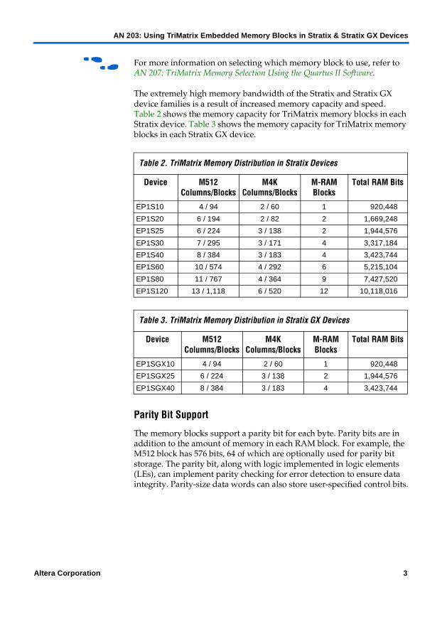
The extremely high memory bandwidth of the Stratix and Stratix GX device families is a result of increased memory capacity and speed. Table 2 shows the memory capacity for TriMatrix memory blocks in each Stratix device. Table 3 shows the memory capacity for TriMatrix memory blocks in each Stratix GX device.
Parity Bit Support
The memory blocks support a parity bit for each byte. Parity bits are in addition to the amount of memory in each RAM block. For example, the M512 block has 576 bits, 64 of which are optionally used for parity bit storage. The parity bit, along with logic implemented in logic elements (LEs), can implement parity checking for error detection to ensure data integrity. Parity-size data words can also store user-specified control bits.
Table 2. TriMatrix Memory Distribution in Stratix Devices
Device M512Columns/Blocks
M4KColumns/Blocks
M-RAM Blocks
Total RAM Bits
EP1S10 4 / 94 2 / 60 1 920,448
EP1S20 6 / 194 2 / 82 2 1,669,248
EP1S25 6 / 224 3 / 138 2 1,944,576
EP1S30 7 / 295 3 / 171 4 3,317,184
EP1S40 8 / 384 3 / 183 4 3,423,744
EP1S60 10 / 574 4 / 292 6 5,215,104
EP1S80 11 / 767 4 / 364 9 7,427,520
EP1S120 13 / 1,118 6 / 520 12 10,118,016
Table 3. TriMatrix Memory Distribution in Stratix GX Devices
Device M512Columns/Blocks
M4KColumns/Blocks
M-RAM Blocks
Total RAM Bits
EP1SGX10 4 / 94 2 / 60 1 920,448
EP1SGX25 6 / 224 3 / 138 2 1,944,576
EP1SGX40 8 / 384 3 / 183 4 3,423,744
Altera Corporation 3

AN 203: Using TriMatrix Embedded Memory Blocks in Stratix & Stratix GX Devices
Byte Enable Support
In the M4K and M-RAM blocks, byte enables can mask the input data so that only specific bytes of data are written. The unwritten bytes retain the previous written value. The write enable signals (wren), in conjunction with the byte enable signals (byteena), controls the RAM block’s write operations. The default value for the byteena signals is high (enabled), in which case writing is controlled only by the wren signals.
Asserting the clear port of the byte enable registers drives the byte enable signals to their default high level.
M4K Blocks
M4K blocks support byte writes when the write port has a data width of 16, 18, 32, or 36 bits. Table 4 summarizes the byte selection.
Note to Table 4:(1) Any combination of byte enables is possible.(2) Byte enables can be used in the same manner with 8-bit words, i.e., in ×16 and ×32
modes.
Table 4. Byte Enable for M4K Blocks Notes (1), (2)
byteena datain ×18 datain ×36
[0] = 1 [8..0] [8..0]
[1] = 1 [17..9] [17..9]
[2] = 1 – [26..18]
[3] = 1 – [35..27]
4 Altera Corporation

AN 203: Using TriMatrix Embedded Memory Blocks in Stratix & Stratix GX Devices
M-RAM Blocks
M-RAM blocks support byte enables for the ×16, ×18, ×32, ×36, ×64, and ×72 modes. In the ×128 or ×144 simple dual-port mode, the two sets of byteena signals (byteena_a and byteena_b) combine to form the necessary 16 byte enables. Tables 5 and 6 summarize the byte selection.
Notes to Table 5:(1) Any combination of byte enables is possible.(2) Byte enables can be used in the same manner with 8-bit words, i.e., in ×16, ×32, and
×64 modes.
Table 5. Byte Enable for M-RAM Blocks Notes (1), (2)
byteena datain ×18 datain ×36 datain ×72
[0] = 1 [8..0] [8..0] [8..0]
[1] = 1 [17..9] [17..9] [17..9]
[2] = 1 – [26..18] [26..18]
[3] = 1 – [35..27] [35..27]
[4] = 1 – – [44..36]
[5] = 1 – – [53..45]
[6] = 1 – – [62..54]
[7] = 1 – – [71..63]
Altera Corporation 5

AN 203: Using TriMatrix Embedded Memory Blocks in Stratix & Stratix GX Devices
.
Notes to Table 6:(1) Any combination of byte enables is possible.(2) Byte enables can be used in the same manner with 8-bit words, i.e., in ×16, ×32, ×64,
and ×128 modes.
Byte Enable Functional Waveform
Figure 1 shows how both the wren and the byteena signals control the write operations of the RAM.
Table 6. M-RAM Combined Byte Selection for ×144 Mode Notes (1), (2)
byteena_a datain ×144
[0] = 1 [8..0]
[1] = 1 [17..9]
[2] = 1 [26..18]
[3] = 1 [35..27]
[4] = 1 [44..36]
[5] = 1 [53..45]
[6] = 1 [62..54]
[7] = 1 [71..63]
[8] = 1 [80..72]
[9] = 1 [89..81]
[10] = 1 [98..90]
[11] = 1 [107..99]
[12] = 1 [116..108]
[13] = 1 [125..117]
[14] = 1 [134..126]
[15] = 1 [143..135]
6 Altera Corporation

AN 203: Using TriMatrix Embedded Memory Blocks in Stratix & Stratix GX Devices
Figure 1. Byte Enable Functional Waveform Note (1)
Note to Figure 1:(1) For more information on simulation output when a read-during-write occurs at the same address location, refer to
“Read-during-Write Operation at the Same Address” on page 26.
Using TriMatrix Memory
The TriMatrix memory blocks include input registers that synchronize writes and output registers to pipeline designs and improve system performance. All TriMatrix memory blocks are fully synchronous, meaning that all inputs are registered, but outputs are either registered or combinatorial. TriMatrix memory can emulate asynchronous memory.
f For more information, refer to AN 210: Converting Memory from Asynchronous to Synchronous for Stratix & Stratix GX Designs.
Depending on the TriMatrix memory block type, the memory can have various modes, including:
■ Single-port■ Simple dual-port■ True dual-port (bidirectional dual-port)■ Shift-register■ ROM■ FIFO
inclock
wren
address
data_in
asynch_data_out
an
XXXX
a0 a1 a2 a0 a1 a2
doutn ABXX XXCD ABCD ABFF FFCD
ABCD
byteena XX 10 01 11
XXXX
XX
ABCD
ABCDFFFF
FFFF
FFFF
ABFF
FFCD
contents at a0
contents at a1
contents at a2
Altera Corporation 7

AN 203: Using TriMatrix Embedded Memory Blocks in Stratix & Stratix GX Devices
Implementing Single-Port Mode
Single-port mode supports non-simultaneous reads and writes. Figure 2 shows the single-port memory configuration for TriMatrix memory. All memory block types support the single-port mode.
Figure 2. Single-Port Memory Note (1)
Note to Figure 2:(1) Two single-port memory blocks can be implemented in a single M4K block.
M4K memory blocks can also be divided in half and used for two independent single-port RAM blocks. The AlteraR QuartusR II software automatically uses this single-port memory packing when running low on memory resources. To force two single-port memories into one M4K block, first ensure that each of the two independent RAM blocks is equal to or less than half the size of the M4K block. Second, assign both single-port RAMs to the same M4K block.
In the single-port RAM configuration, the outputs can only be in read-during-write mode, which means that during the write operation, data written to the RAM flows through to the RAM outputs. When the output registers are bypassed, the new data is available on the rising edge of the same clock cycle it was written on. For more information about read-during-write mode, refer to “Read-during-Write Operation at the Same Address” on page 26.
Figure 3 shows timing waveforms for read and write operations in single-port mode.
data[ ]address[ ]wren inclockinclockeninaclr
q[ ]outclock outclocken
outaclr
8 Altera Corporation

AN 203: Using TriMatrix Embedded Memory Blocks in Stratix & Stratix GX Devices
Figure 3. Single-Port Timing Waveforms
Implementing Simple Dual-Port Mode
Simple dual-port memory supports a simultaneous read and write. Figure 4 shows the simple dual-port memory configuration for TriMatrix memory. All memory block types support this configuration.
Figure 4. Simple Dual-Port Memory Note (1)
Note to Figure 4:(1) Simple dual-port RAM supports read/write clock mode in addition to the
input/output clock mode shown.
in clock
wren
address
data_in
synch_data_out
an-1
din-1 din din4 din5
a6
din6
an a0 a1 a2 a3 a4 a5
asynch_data_out
din-2 din-1 din dout0 dout1 dout2 dout3 din4
din-1 din dout0 dout1 dout2 dout3 din4 din5
data[ ]wraddress[ ]wren inclockinclockeninaclr
rdaddress[ ]rden
q[ ]outclock outclocken
outaclr
Dual-Port Memory
Altera Corporation 9

AN 203: Using TriMatrix Embedded Memory Blocks in Stratix & Stratix GX Devices
TriMatrix memory supports mixed-width configurations, allowing different read and write port widths. Tables 7 to 9 show the mixed width configurations for the M512, M4K, and M-RAM blocks, respectively.
Table 7. M512 Block Mixed-Width Configurations (Simple Dual-Port Mode)
Read Port Write Port
512 × 1 256 × 2 128 × 4 64 × 8 32 × 16 64 × 9 32 × 18
512 × 1 v v v v v
256 × 2 v v v v v
128 × 4 v v v v
64 × 8 v v v
32 × 16 v v v v
64 × 9 v
32 × 18 v
Table 8. M4K Block Mixed-Width Configurations (Simple Dual-Port Mode)
Read Port Write Port
4K × 1 2K × 2 1K × 4 512 × 8 256 × 16 128 × 32 512 × 9 256 × 18 128 × 36
4K × 1 v v v v v v
2K × 2 v v v v v v
1K × 4 v v v v v v
512 × 8 v v v v v v
256 × 16 v v v v v v
128 × 32 v v v v v v
512 × 9 v v v
256 × 18 v v v
128 × 36 v v v
10 Altera Corporation

AN 203: Using TriMatrix Embedded Memory Blocks in Stratix & Stratix GX Devices
M512 blocks support serializer and deserializer (SERDES) applications. By using the mixed-width support in combination with double data rate (DDR) I/O standards, the block can function as a SERDES to support low-speed serial I/O standards using global or regional clocks.
f For more information on Stratix device I/O structure refer to the Stratix Programmable Logic Device Family Data Sheet. For more information on Stratix GX device I/O structure refer to the Stratix GX FPGA Family Data Sheet.
In simple dual-port mode, the M512 and M4K blocks have one write enable and one read enable signal. The M512 does not support a clear port on the rden register. On the M4K block, asserting the clear port of the rden register drives rden high, which allows the read operation to occur. When the read enable is deactivated, the current data is retained at the output ports. If the read enable is activated during a write operation with the same address location selected, the simple dual-port RAM output is either unknown or can be set to output the old data stored at the memory address. For more information, refer to “Read-during-Write Operation at the Same Address” on page 26.
M-RAM blocks have one write enable signal in simple dual-port mode. To perform a write operation, the write enable is held high. The M-RAM block is always enabled for read operation. If the read address and the write address select the same address location during a write operation, the M-RAM block output is unknown.
Figure 5 shows timing waveforms for read and write operations in simple dual-port mode.
Table 9. M-RAM Block Mixed-Width Configurations (Simple Dual-Port Mode)
Read Port Write Port
64K × 9 32K × 18 16K × 36 8K × 72 4K × 144
64K × 9 v v v v
32K × 18 v v v v
16K × 36 v v v v
8K × 72 v v v v
4K × 144 v
Altera Corporation 11

AN 203: Using TriMatrix Embedded Memory Blocks in Stratix & Stratix GX Devices
Figure 5. Simple Dual-Port Timing Waveforms Note (1)
Note to Figure 5:(1) The rden signal is not available in the M-RAM block. A M-RAM block in simple dual-port mode is always reading
out the data stored at the current read address location.
Implementing True Dual-Port Mode
M4K and M-RAM blocks offer a true dual-port mode to support any combination of two-port operations: two reads, two writes, or one read and one write at two different clock frequencies. Figure 6 shows the true dual-port memory configuration for TriMatrix memory.
Figure 6. True Dual-Port Memory Note (1)
Note to Figure 6:(1) True dual-port memory supports input/output clock mode in addition to the
independent clock mode shown.
wrclock
wren
wraddress
data_in
synch_data_out
an-1 an a0 a1 a2 a3 a4 a5
din-1 din din4 din5
rdclock
a6
din6
asynch_data_out
rden
rdaddress bn b0 b1 b2 b3
doutn-2 doutn-1 doutn
doutn-1 doutn dout0
dataA[ ]addressA[ ]wrenA
clockA
clockenA
qA[ ]aclrA
dataB[ ]addressB[ ]
wrenB
clockB clockenB
qB[ ]aclrB
A B
12 Altera Corporation
AN 203: Using TriMatrix Embedded Memory Blocks in Stratix & Stratix GX Devices
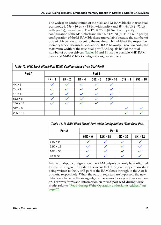
The widest bit configuration of the M4K and M-RAM blocks in true dual-port mode is 256 × 16-bit (× 18-bit with parity) and 8K × 64-bit (× 72-bit with parity), respectively. The 128 × 32-bit (× 36-bit with parity) configuration of the M4K block and the 4K × 128-bit (× 144-bit with parity) configuration of the M-RAM block are unavailable because the number of output drivers is equivalent to the maximum bit width of the respective memory block. Because true dual-port RAM has outputs on two ports, the maximum width of the true dual-port RAM equals half of the total number of output drivers. Tables 10 and 11 list the possible M4K RAM block and M-RAM block configurations, respectively.
In true dual-port configuration, the RAM outputs can only be configured for read-during-write mode. This means that during write operation, data being written to the A or B port of the RAM flows through to the A or B outputs, respectively. When the output registers are bypassed, the new data is available on the rising edge of the same clock cycle it was written on. For waveforms and information on mixed-port read-during-write mode, refer to “Read-during-Write Operation at the Same Address” on page 26.
Table 10. M4K Block Mixed-Port Width Configurations (True Dual-Port)
Port A Port B
4K × 1 2K × 2 1K × 4 512 × 8 256 × 16 512 × 9 256 × 18
4K × 1 v v v v v
2K × 2 v v v v v
1K × 4 v v v v v
512 × 8 v v v v v
256 × 16 v v v v v
512 × 9 v v
256 × 18 v v
Table 11. M-RAM Block Mixed-Port Width Configurations (True Dual-Port)
Port A Port B
64K × 9 32K × 18 16K × 36 8K × 72
64K × 9 v v v v
32K × 18 v v v v
16K × 36 v v v v
8K × 72 v v v v
Altera Corporation 13
AN 203: Using TriMatrix Embedded Memory Blocks in Stratix & Stratix GX Devices
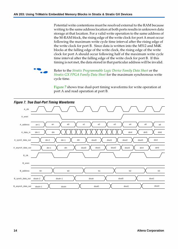
Potential write contentions must be resolved external to the RAM because writing to the same address location at both ports results in unknown data storage at that location. For a valid write operation to the same address of the M-RAM block, the rising edge of the write clock for port A must occur following the maximum write cycle time interval after the rising edge of the write clock for port B. Since data is written into the M512 and M4K blocks at the falling edge of the write clock, the rising edge of the write clock for port A should occur following half of the maximum write cycle time interval after the falling edge of the write clock for port B. If this timing is not met, the data stored in that particular address will be invalid.
f Refer to the Stratix Programmable Logic Device Family Data Sheet or the Stratix GX FPGA Family Data Sheet for the maximum synchronous write cycle time.
Figure 7 shows true dual-port timing waveforms for write operation at port A and read operation at port B.
Figure 7. True Dual-Port Timing Waveforms
A_clk
A_wren
A_address
A_data_in
B_synch_data_out
an-1 an a0 a1 a2 a3 a4 a5
din-1 din din4 din5
B_clk
a6
din6
B_asynch_data_out
B_wren
B_address bn b0 b1 b2 b3
doutn-2 doutn-1 doutn
doutn-1 doutn dout0
A_synch_data_out
A_asynch_data_out
dout0
dout1
dout1
dout2
din-2 din-1 din dout0 dout1 dout2 dout3 din4
din-1 din dout0 dout1 dout2 dout3 din4 din5
14 Altera Corporation

AN 203: Using TriMatrix Embedded Memory Blocks in Stratix & Stratix GX Devices
Implementing Shift-Register Mode
Embedded memory block configurations can implement shift registers for digital signal processing (DSP) applications, such as finite impulse response (FIR) filters, pseudo-random number generators, multi-channel filtering, and auto-correlation and cross-correlation functions. These and other DSP applications require local data storage, traditionally implemented with standard flip-flops that can quickly consume many logic cells for large shift registers. A more efficient alternative is to use embedded memory as a shift register block, which saves logic cell and routing resources and provides a more efficient implementation.
The size of a (w × m × n) shift register is determined by the input data width (w), the length of the taps (m), and the number of taps (n). The size of a (w × m × n) shift register must be less than or equal to the maximum number of memory bits in the respective block: 576 bits for the M512 block and 4,608 bits for the M4K block. In addition, the size of w × n must be less than or equal to the maximum width of the respective block: 18 bits for the M512 block and 36 bits for the M4K block. If a larger shift register is required, the memory blocks can be cascaded together.
1 M-RAM blocks do not support the shift-register mode.
Data is written into each address location at the falling edge of the clock and read from the address at the rising edge of the clock. The shift-register mode logic automatically controls the positive and negative edge clocking to shift the data in one clock cycle. Figure 8 shows the TriMatrix memory block in the shift-register mode.
Altera Corporation 15

AN 203: Using TriMatrix Embedded Memory Blocks in Stratix & Stratix GX Devices
Figure 8. Shift-Register Memory Configuration
Implementing ROM Mode
The M512 and the M4K blocks support ROM mode. Use a memory initialization file (.mif) to initialize the ROM contents of M512 and M4K blocks. The M-RAM block does not support ROM mode.
All Stratix memory configurations must have synchronous inputs; therefore, the address lines of the ROM are registered. The outputs can be registered or combinatorial. The ROM read operation is identical to the read operation in the single-port RAM configuration.
Implementing FIFO Buffers
While the small M512 memory blocks are ideal for designs with many shallow FIFO buffers, all three memory sizes support FIFO mode.
m-Bit Shift Registerw w
m-Bit Shift Register
m-Bit Shift Register
m-Bit Shift Register
w w
w w
w w
w × m × n Shift Register
n Numberof Taps
16 Altera Corporation

AN 203: Using TriMatrix Embedded Memory Blocks in Stratix & Stratix GX Devices
All memory configurations have synchronous inputs; however, the FIFO buffer outputs are always combinatorial. Simultaneous read and write from an empty FIFO is not supported.
Clock Modes Depending on the TriMatrix memory mode, independent, input/output, read/write, and/or single-port clock modes are available. Table 12 shows the clock modes supported by the TriMatrix memory modes.
Independent Clock Mode
The TriMatrix memory blocks can implement independent clock mode for true dual-port memory. In this mode, a separate clock is available for each port (A and B). Clock A controls all registers on the port A side, while clock B controls all registers on the port B side. Each port also supports independent clock enables and asynchronous clear signals for port A and B registers. Figure 9 shows a TriMatrix memory block in independent clock mode.
Table 12. TriMatrix Memory Clock Modes
Clocking Mode True-Dual Port Mode
Simple Dual-Port Mode
Single-Port Mode
Independent v
Input/output v v
Read/write v
Single-port v
Altera Corporation 17

AN 203: Using TriMatrix Embedded Memory Blocks in Stratix & Stratix GX Devices
Figure 9. Independent Clock Mode
8D E
NA
Q
D EN
A
Q
D EN
A
Q
data
A[ ]
addr
ess A
[ ]
Mem
ory
Blo
ck25
6 ´
16 (
2)51
2 ´
81,
024
´ 4
2,04
8 ´
24,
096
´ 1
Dat
a In
Add
ress
A
Writ
e/R
ead
Ena
ble
Dat
a O
ut
Dat
a In
Add
ress
B
Writ
e/R
ead
Ena
ble
Dat
a O
ut
clke
n A
cloc
k A
D EN
A
Q
wre
n A
8 LA
B R
ow C
lock
s
q A[ ]
8da
taB[ ]
addr
ess B
[ ]
clke
n B
cloc
k B
wre
n B
q B[ ]
EN
A
AB
EN
ADQ
D EN
A
Qby
teen
a A[ ]
Byt
e E
nabl
e A
Byt
e E
nabl
e B
byte
ena B
[ ]
EN
ADQ
EN
ADQ
EN
ADQ
DQ
Writ
eP
ulse
Gen
erat
or
Writ
eP
ulse
Gen
erat
or
18 Altera Corporation
AN 203: Using TriMatrix Embedded Memory Blocks in Stratix & Stratix GX Devices
Input/Output Clock Mode
The TriMatrix memory blocks can implement input/output clock mode for true and simple dual-port memory. On each of the two ports, A and B, one clock controls all registers for inputs into the memory block: data input, wren, and address. The other clock controls the block’s data output registers. Each memory block port also supports independent clock enables and asynchronous clear signals for input and output registers. Figures 10 and 11 show the memory block in input/output clock mode for true and simple dual-port modes, respectively.
Altera Corporation 19

AN 203: Using TriMatrix Embedded Memory Blocks in Stratix & Stratix GX Devices
Figure 10. Input/Output Clock Mode in True Dual-Port Mode
8
D EN
A
Q
D EN
A
Q
D EN
A
Q
data
A[ ]
addr
ess A
[ ]
Mem
ory
Blo
ck25
6 ×
16 (2
)51
2 ×
81,
024
× 4
2,04
8 ×
24,
096
× 1
Dat
a In
Add
ress
A
Writ
e/R
ead
Ena
ble
Dat
a O
ut
Dat
a In
Add
ress
B
Writ
e/R
ead
Ena
ble
Dat
a O
ut
clke
n A
cloc
k A
D EN
A
Q
wre
n A
8 LA
B R
ow C
lock
s
q A[ ]
8
data
B[ ]
addr
ess B
[ ]
clke
n B
cloc
k B
wre
n B
q B[ ]
EN
A
AB
EN
ADQ
EN
ADQ
EN
ADQ
DQ
D EN
A
Qby
teen
a A[ ]
Byt
e E
nabl
e A
Byt
e E
nabl
e B
byte
ena B
[ ]
EN
ADQ
Writ
eP
ulse
Gen
erat
or
Writ
eP
ulse
Gen
erat
or
20 Altera Corporation

AN 203: Using TriMatrix Embedded Memory Blocks in Stratix & Stratix GX Devices
Figure 11. Input/Output Clock Mode in Simple Dual-Port Mode Notes (1), (2)
Notes to Figure 11:(1) The rden signal is not available in the M-RAM block. A M-RAM block in simple dual-port mode is always reading
out the data stored at the current read address location.(2) For more information on the MultiTrack™ interconnect, refer to the Stratix Programmable Logic Device Family Data
Sheet or the Stratix GX FPGA Family Data Sheet.
8
DENA
Q
D
ENA
Q
D
ENA
Q
D
ENA
Q
DENA
Q
data[ ]
DENA
Qwraddress[ ]
address[ ]
Memory Block256 ´ 16
512 ´ 81,024 ´ 42,048 ´ 24,096 ´ 1
Data In
Read Address
Write Address
Write Enable
Read Enable
Data Out
outclken
inclken
wrclock
rdclock
wren
rden
8 LAB Row Clocks
To MultiTrackInterconnect
DENA
Qbyteena[ ] Byte Enable
WritePulse
Generator
Altera Corporation 21

AN 203: Using TriMatrix Embedded Memory Blocks in Stratix & Stratix GX Devices
Read/Write Clock Mode
The TriMatrix memory blocks can implement read/write clock mode for simple dual-port memory. This mode can use up to two clocks. The write clock controls the block’s data inputs, wraddress, and wren. The read clock controls the data output, rdaddress, and rden. The memory blocks support independent clock enables for each clock and asynchronous clear signals for the read- and write-side registers. Figure 12 shows a memory block in read/write clock mode.
22 Altera Corporation

AN 203: Using TriMatrix Embedded Memory Blocks in Stratix & Stratix GX Devices
Figure 12. Read/Write Clock Mode in Simple Dual-Port Mode Note (1)
Note to Figure 12:(1) For more information on the MultiTrack interconnect, see the Stratix Programmable Logic Device Family Data Sheet or
the Stratix GX FPGA Family Data Sheet.
Single-Port Mode
The TriMatrix memory blocks can implement single-port clock mode for single-port memory mode. Single-port mode is used when simultaneous reads and writes are not required. See Figure 13. A single block in a memory block can support up to two single-port mode RAM blocks in M4K blocks.
8
DENA
Q
D
ENA
Q
D
ENA
Q
D
ENA
Q
DENA
Q
data[ ]
DENA
Qwraddress[ ]
address[ ]
Memory Block256 × 16
512 × 81,024 × 42,048 × 24,096 × 1
Data In
Read Address
Write Address
Write Enable
Read Enable
Data Out
outclken
inclken
wrclock
rdclock
wren
rden
8 LAB RowClocks
To MultiTrackInterconnect
DENA
Qbyteena[ ] Byte Enable
WritePulse
Generator
Altera Corporation 23

AN 203: Using TriMatrix Embedded Memory Blocks in Stratix & Stratix GX Devices
Figure 13. Single-Port Mode Note (1)
Note to Figure 13:(1) For more information on the MultiTrack interconnect, refer to the Stratix Programmable Logic Device Family Data Sheet
or the Stratix GX FPGA Family Data Sheet.
Designing With TriMatrix Memory
When instantiating TriMatrix memory the designer must understand the various features that set it apart from other memory architectures. The following sections describe some of the important attributes and functionality of TriMatrix memory.
f For information on the difference between APEXR-style memory and TriMatrix memory, refer to AN 206: Transitioning APEX Deisgns to Stratix Devices.
8
DENA
Q
D
ENA
Q
D
ENA
Q
DENA
Q
data[ ]
address[ ]
RAM/ROM256 × 16
512 × 81,024 × 42,048 × 24,096 × 1
Data In
Address
Write Enable
Data Out
outclken
inclken
inclock
outclock
WritePulse
Generator
wren
8 LAB RowClocks
To MultiTrackInterconnect
24 Altera Corporation

AN 203: Using TriMatrix Embedded Memory Blocks in Stratix & Stratix GX Devices
Selecting TriMatrix Memory Blocks
The Quartus II software automatically partitions user-defined memory into embedded memory blocks using the most efficient size combinations. The memory can also be manually assigned to a specific block size or a mixture of block sizes. Table 1 on page 2 is a guide for selecting a TriMatrix memory block size based on supported features.
f For more information on selecting which memory block to use, refer to Application Note 207 (TriMatrix Memory Selection Using the Quartus II Software)
Synchronous & Pseudo-Asynchronous Modes
TriMatrix memory architecture implements synchronous (pipelined) RAM by registering both the input and output signals to the RAM block. All TriMatrix memory inputs are registered providing synchronous write cycles. In synchronous operation, RAM generates its own self-timed strobe write enable (wren) signal derived from the global or regional clock. In contrast, a circuit using asynchronous RAM must generate the RAM wren signal while ensuring its data and address signals meet setup and hold time specifications relative to the wren signal. The output registers can be bypassed.
In an asynchronous memory neither the input nor the output is registered. While Stratix and Stratix GX devices do not support asynchronous memory, they do support a pseudo-asynchronous read where the output data is available during the clock cycle when the read address is driven into it. Pseudo-asynchronous reading is possible in the simple and true dual-port modes of the M512 and M4K blocks by clocking the read enable and read address registers on the negative clock edge and bypassing the output registers.
f For more information, refer to AN 210: Converting Memory from Asynchronous to Synchronous for Stratix & Stratix GX Devices.
Power-up Conditions & Memory Initialization
Upon power-up, TriMatrix memory is in an idle state. The M512 and M4K block outputs always power-up to zero, regardless of whether the output registers are used or bypassed. Even if a memory initialization file is used to pre-load the contents of the RAM block, the outputs will still power-up cleared. For example, if address 0 is pre-initialized to FF, the M512 and M4K blocks power-up with the output at 00.
Altera Corporation 25

AN 203: Using TriMatrix Embedded Memory Blocks in Stratix & Stratix GX Devices
M-RAM blocks do not support memory initialization files; therefore, they cannot be pre-loaded with data upon power-up. M-RAM blocks combinatorial outputs and memory controls always power-up to an unknown state. If M-RAM block outputs are registered, the registers power-up cleared. The undefined output appears one clock cycle later. The output remains undefined until a read operation is performed on an address that has been written to.
Read-during-Write Operation at the Same Address
The following two sections describe the functionality of the various RAM configurations when reading from an address during a write operation at that same address. There are two types of read-during-write operations: same-port and mixed-port. Figure 14 illustrates the difference in data flow between same-port and mixed-port read-during-write.
Figure 14. Read-during-Write Data Flow
Same-Port Read-during-Write Mode
For read-during-write operation of a single-port RAM or the same port of a true dual-port RAM, the new data is available on the rising edge of the same clock cycle it was written on. This behavior is valid on all memory-block sizes. See Figure 15 for a sample functional waveform.
When using byte enables in true dual-port RAM mode, the outputs for the masked bytes on the same port are unknown. (See Figure 1 on page 7.) The non-masked bytes are read out as shown in Figure 15.
Port Adata in
Port Bdata in
Port Bdata out
Port Adata out
Same-portdata flow
Mixed-portdata flow
26 Altera Corporation

AN 203: Using TriMatrix Embedded Memory Blocks in Stratix & Stratix GX Devices
Figure 15. Same-Port Read-during-Write Functionality Note (1)
Note to Figure 15:(1) Outputs are not registered.
Mixed-Port Read-during-Write Mode
This mode is used when a RAM in simple or true dual-port mode has one port reading and the other port writing to the same address location with the same clock.
The READ_DURING_WRITE_MODE_MIXED_PORTS parameter for M512 and M4K memory blocks determines whether to output the old data at the address or a “don’t care” value. Setting this parameter to OLD_DATA outputs the old data at that address. Setting this parameter to DONT_CARE outputs a “don’t care” or unknown value. See Figures 16 and 17 for sample functional waveforms showing this operation. These figures assume that the outputs are not registered.
The DONT_CARE setting allows memory implementation in any TriMatrix memory block. The OLD_DATA setting restricts memory implementation to only M512 or M4K memory blocks. Selecting DONT_CARE gives the compiler more flexibility when placing memory functions into TriMatrix memory.
inclock
data_in
wren
data_out A
BA
Old
Altera Corporation 27

AN 203: Using TriMatrix Embedded Memory Blocks in Stratix & Stratix GX Devices
Figure 16. Mixed-Port Read-during-Write: OLD_DATA
For mixed-port read-during-write operation of the same address location of a M-RAM block, the RAM outputs are unknown, as shown in Figure 17.
Figure 17. Mixed-Port Read-during-Write: DONT_CARE
When two different clocks are used in a dual-port RAM, the read-during-write behavior depends on the relationship of the clocks. For the M512 and M4K blocks, the writing of the new contents starts at the falling edge of the write clock. Therefore, if the read clock’s rising edge occurs at any point up to the falling edge of the write clock, the old data is read out. If the read clock’s rising edge occurs between the falling edge of the write clock and half the maximum write cycle time interval, the output is unknown data.
f For the maximum synchronous write cycle time refer to the Stratix Programmable Logic Device Family Data Sheet or the Stratix GX FPGA Family Data Sheet.
inclock
Port Adata_in
Port Awren
Port Bdata_out
A B
AOld
Port Bwren
B
Address QaddressA and
addressB
inclock
Port Adata_in
Port Awren
Port Bdata_out
A B
BUnknown
Port Bwren
Address QaddressA and
addressB
28 Altera Corporation

AN 203: Using TriMatrix Embedded Memory Blocks in Stratix & Stratix GX Devices
For the M-RAM block, if the read clock’s rising edge occurs more than the maximum write cycle time interval after the rising edge of the write clock and the maximum write cycle time interval, the output is new data. If the read clock rising edge occurs between the rising edge of the write clock and the maximum write cycle time interval, the output is unknown data.
f For the maximum synchronous write cycle time refer to the Stratix Programmable Logic Device Family Data Sheet or the Stratix GX FPGA Family Data Sheet.
Conclusion TriMatrix memory, an enhanced RAM architecture with extremely high memory bandwidth in Stratix and Stratix GX devices, gives advanced control of memory applications with features such as byte enables, parity bit storage, and shift-register mode, as well as mixed-port width support and true dual-port mode.
Revision History
The information contained in AN 203: Using TriMatrix Embedded Memory Blocks in Stratix & Stratix GX Devices version 2.0 supersedes information published in previous versions. The following change was made in AN 203: Using TriMatrix Embedded Memory Blocks in Stratix & Stratix GX Devices version 2.0: added Stratix GX devices throughout the document.
Altera Corporation 29
101 Innovation DriveSan Jose, CA 95134(408) 544-7000http://www.altera.comApplications Hotline:(800) 800-EPLDLiterature Services:[email protected]
Copyright © 2002 Altera Corporation. All rights reserved. Altera, The Programmable Solutions Company, thestylized Altera logo, specific device designations, and all other words and logos that are identified astrademarks and/or service marks are, unless noted otherwise, the trademarks and service marks of AlteraCorporation in the U.S. and other countries. All other product or service names are the property of theirrespective holders. Altera products are protected under numerous U.S. and foreign patents and pendingapplications, maskwork rights, and copyrights. Altera warrants performance of itssemiconductor products to current specifications in accordance with Altera's standardwarranty, but reserves the right to make changes to any products and services at any timewithout notice. Altera assumes no responsibility or liability arising out of the applicationor use of any information, product, or service described herein except as expressly agreedto in writing by Altera Corporation. Altera customers are advised to obtain the latestversion of device specifications before relying on any published information and beforeplacing orders for products or services


![Intel® AVX-512 Architecture - LLVM...A0 A1 A2 A3 A1 A2 A3 A6 A4 A5 A6 A7 A7 Mask: k[] = 01110011 Zeroed in the ss register form X A0 A1 A2 A0 A1 A2 A3 X X A3 A4 A4 Mask: k[] = 01110011](https://cdn.vdocuments.us/doc/165x107/5f31b370c034de36036a9e97/intel-avx-512-architecture-llvm-a0-a1-a2-a3-a1-a2-a3-a6-a4-a5-a6-a7-a7-mask.jpg)


![JOHN CRISWELL and CHEN DING, arXiv:1810.00905v1 [cs.PL] …branch. The branch jumps to A1 80 times ands jumps to A2 20 times. A1 calls function B but A2 calls function C. M A0 A1 A2](https://cdn.vdocuments.us/doc/165x107/5f8f5b5c0aecd9624521e0c4/john-criswell-and-chen-ding-arxiv181000905v1-cspl-branch-the-branch-jumps.jpg)