www.tyndall.ie
Tyndall National Institute
Tyndall Central Fabrication
Facility (CFF)
IRDG March 2013
www.tyndall.ie
Outline
Tyndall Central Fabrication Facility Flexible collaboration with industry
SensL APDs RADFETs Sicel/GAESi Xenics Silicon photodiode arrays for earth observation QinetiQ/DERA IR Bolometers
Summary
www.tyndall.ie
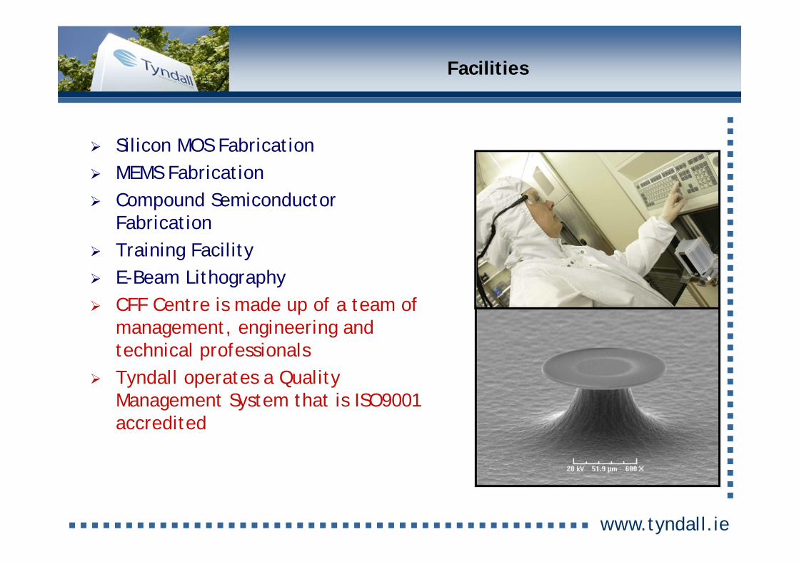
Facilities
Silicon MOS Fabrication MEMS Fabrication Compound Semiconductor
Fabrication Training Facility E-Beam Lithography CFF Centre is made up of a team of
management, engineering and technical professionals
Tyndall operates a Quality Management System that is ISO9001 accredited
www.tyndall.ie
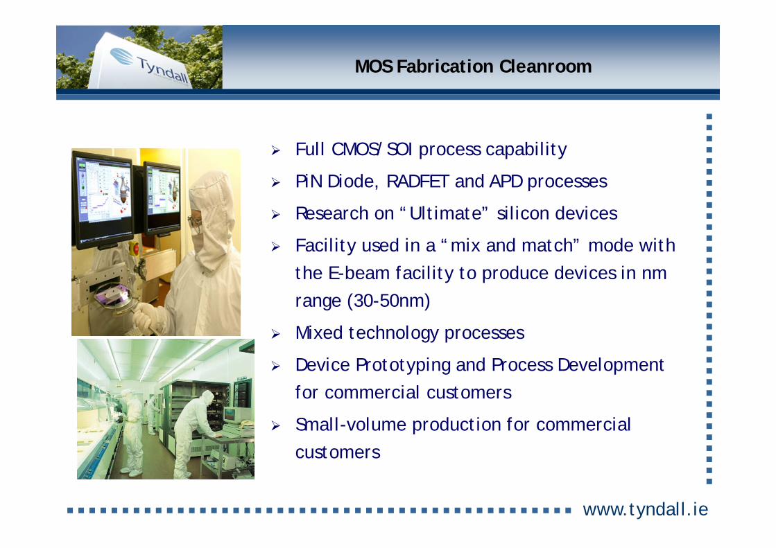
Full CMOS/SOI process capability
PiN Diode, RADFET and APD processes
Research on “Ultimate” silicon devices
Facility used in a “mix and match” mode with the E-beam facility to produce devices in nm range (30-50nm)
Mixed technology processes
Device Prototyping and Process Development for commercial customers
Small-volume production for commercial customers
MOS Fabrication Cleanroom
www.tyndall.ie
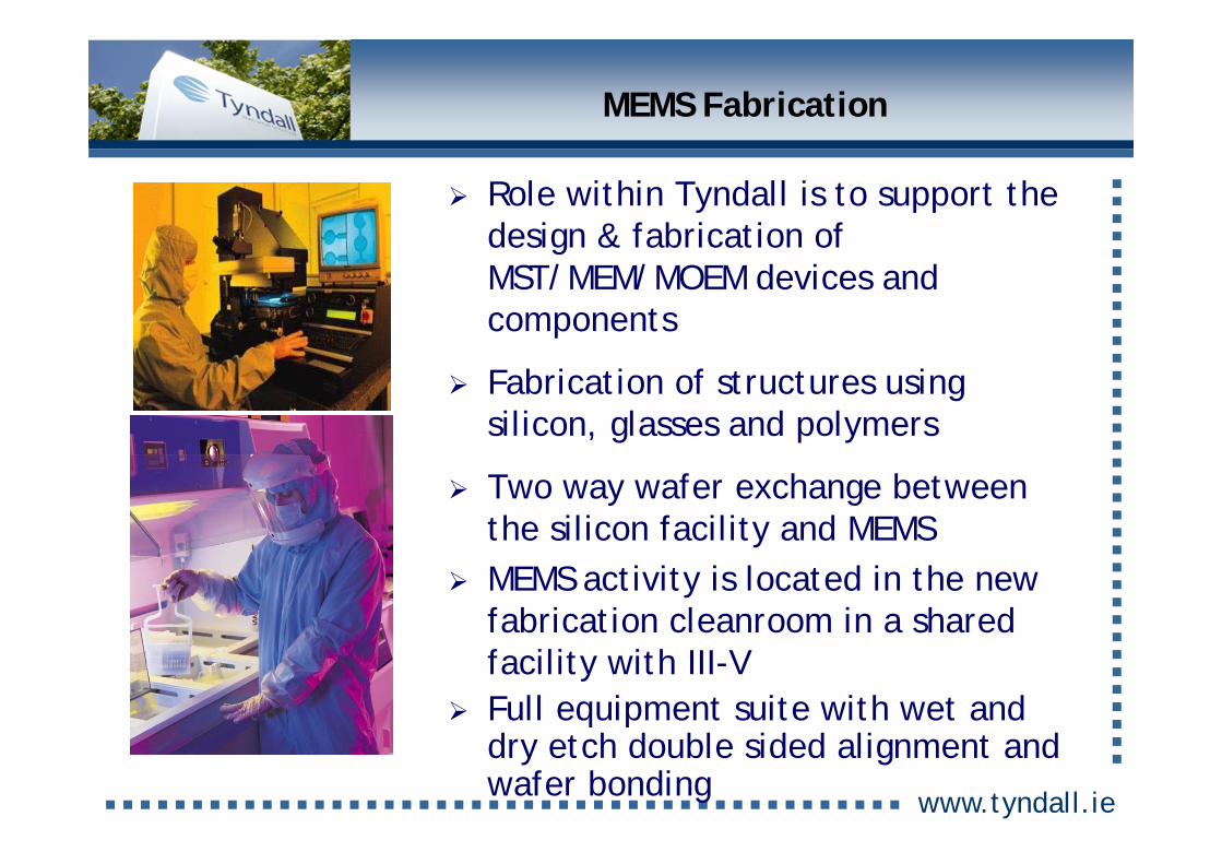
MEMS Fabrication
Role within Tyndall is to support the design & fabrication of MST/MEM/MOEM devices and components
Fabrication of structures using silicon, glasses and polymers
Two way wafer exchange between the silicon facility and MEMS
MEMS activity is located in the new fabrication cleanroom in a shared facility with III-V
Full equipment suite with wet and dry etch double sided alignment and wafer bonding
www.tyndall.ie
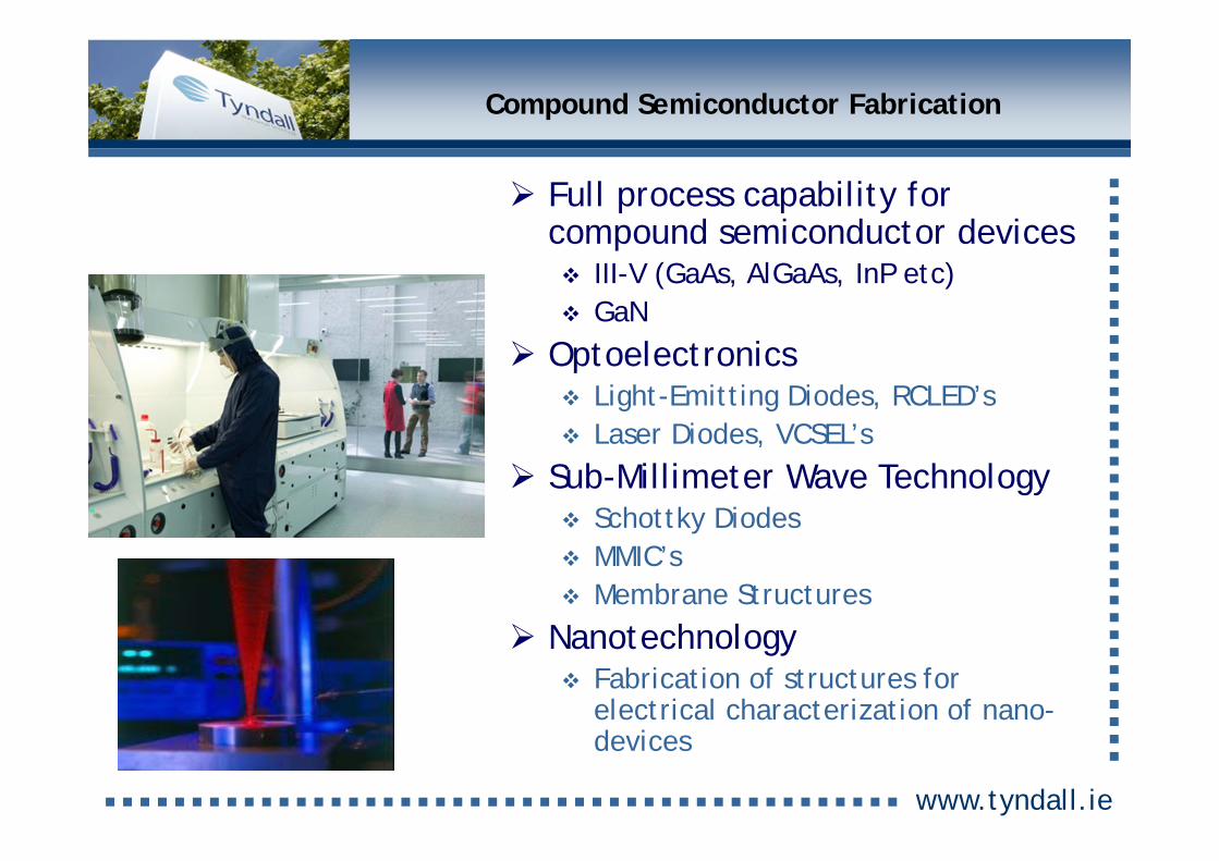
Full process capability for compound semiconductor devices III-V (GaAs, AlGaAs, InP etc) GaN
Optoelectronics Light-Emitting Diodes, RCLED’s Laser Diodes, VCSEL’s
Sub-Millimeter Wave Technology Schottky Diodes MMIC’s Membrane Structures
Nanotechnology Fabrication of structures for
electrical characterization of nano-devices
Compound Semiconductor Fabrication
www.tyndall.ie
Training Fabrication
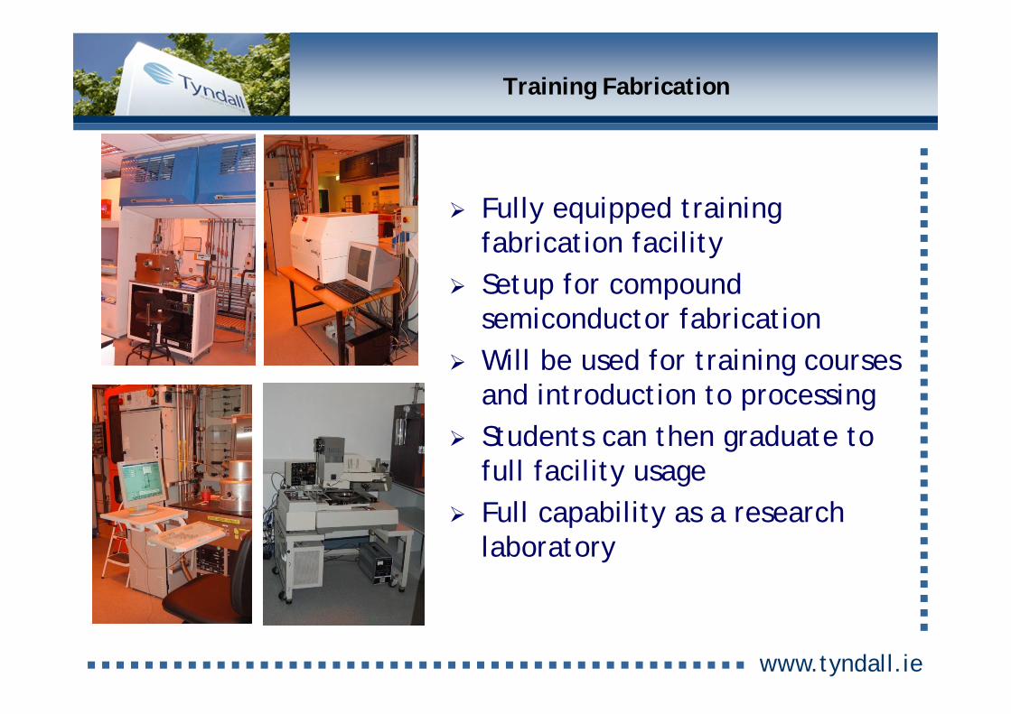
Fully equipped training fabrication facility
Setup for compound semiconductor fabrication
Will be used for training courses and introduction to processing
Students can then graduate to full facility usage
Full capability as a research laboratory

www.tyndall.ie
Flexifab
Capability/Concept rather than a separate space
Allow for the introduction of new materials and process concepts in a controlled environment
Significant amount of new equipment purchased under the PRTLI5 programme (€3.8M) (Project:Tyffani)
Fits with the work in the Advanced Materials group, Nanotechnology and the Photonics Devices groups
Some equipment installed all ordered or identified
www.tyndall.ie
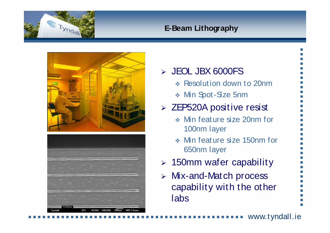
JEOL JBX 6000FS Resolution down to 20nm Min Spot-Size 5nm
ZEP520A positive resist Min feature size 20nm for
100nm layer Min feature size 150nm for
650nm layer
150mm wafer capability Mix-and-Match process
capability with the other labs
E-Beam Lithography
www.tyndall.ie
Other Laboratories Within Tyndall
Ferroelectric/Ferromagnetic growth facility (Atomic Vapour Deposition)
EMAF Microscopy Laboratory High resolution SEM Dual Beam FIB TEM
Electronic test facilities Photonics and electronics packaging capabilities Mechanical workshop Nanotechnology Characterization laboratories
www.tyndall.ie
CASE STUDIES
www.tyndall.ie
SensL
SensL was a spin-out from Tyndall in 2004 An APD process which had been the subject of several
PhD projects was licensed by Tyndall to SensL To become a fully commercial process significant
development had to be carried out Tyndall fabrication staff operated in a close
collaboration with SensL process engineers to develop a process capable of supporting multiple commercial products
From 2004 to 2010 all SensL development and production silicon was fabricated at Tyndall
In 2010 the process was successfully transferred to a commercial foundry

www.tyndall.ie
SensL Technology
SensL are active in the following application areas Medical imaging Homeland security Analytical Instruments
SensL products include Silicon Photomultipliers
• A direct replacement for Linear Photomultiplier Tubes
Photon Counting Systems• High performance photon counting
devices
www.tyndall.ie
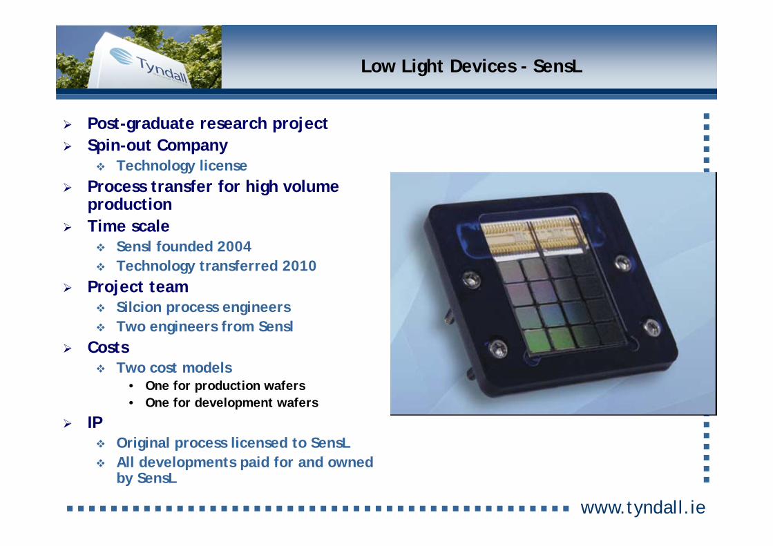
Low Light Devices - SensL
Post-graduate research project Spin-out Company
Technology license Process transfer for high volume
production Time scale
Sensl founded 2004 Technology transferred 2010
Project team Silcion process engineers Two engineers from Sensl
Costs Two cost models
• One for production wafers• One for development wafers
IP Original process licensed to SensL All developments paid for and owned
by SensL
www.tyndall.ie
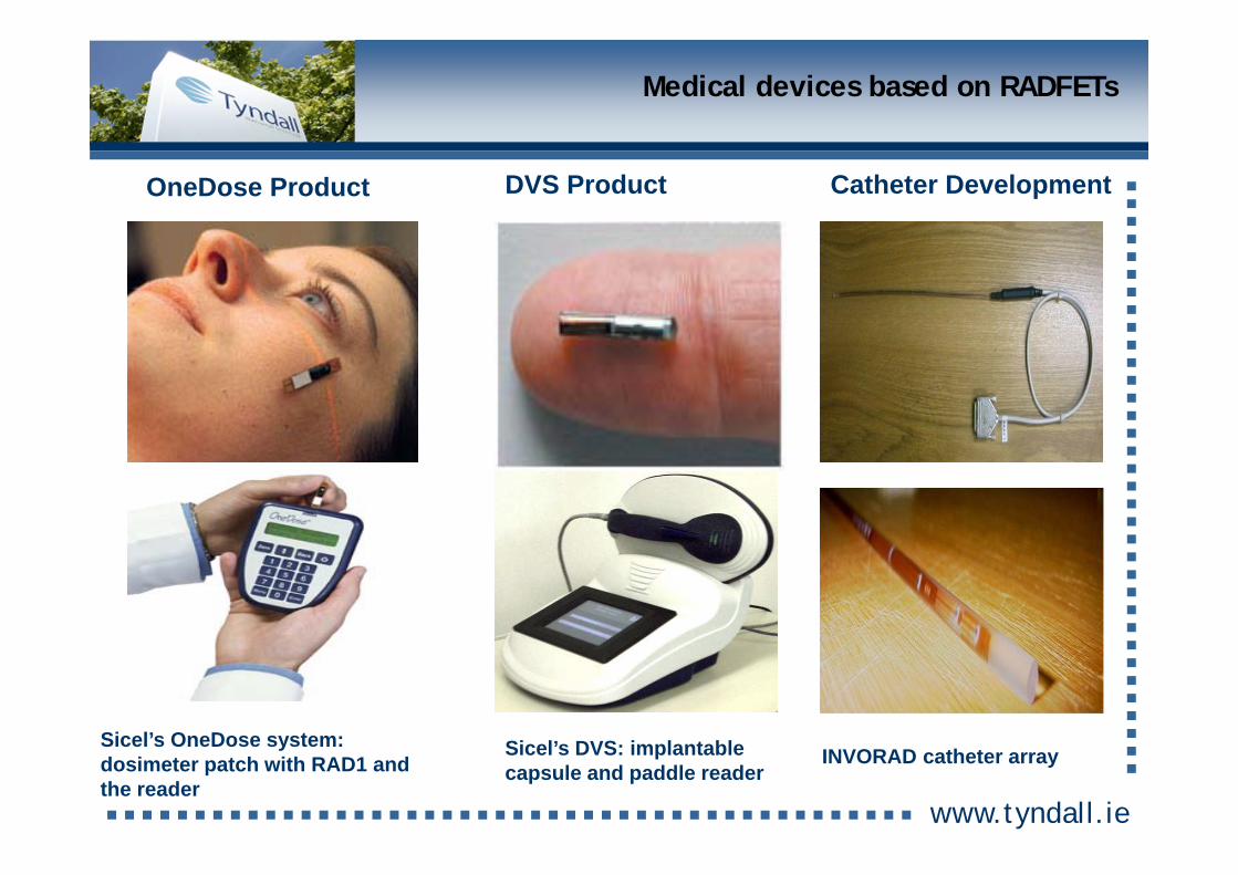
Medical devices based on RADFETs
Sicel’s OneDose system: dosimeter patch with RAD1 and the reader
Sicel’s DVS: implantable capsule and paddle reader
INVORAD catheter array
OneDose Product DVS Product Catheter Development
www.tyndall.ie
Radiation Detection
In the mid-1980s Tyndall (then NMRC) entered an agreement with ESA (ESTEC) to be come the Microelectronics Technology Support Laboratory (MTSL)
As part of that agreement, a simple radiation detector was developed for in-craft housekeeping
This detector monitored the amount of radiation being detected by on-board electronics
The device is very simple MOS device with special processing to make it radiation “soft”
Continued development of this device brought the sensitivity and range into an area suitable for medical applications
Tyndall has also provided RADFETs for personnel monitors in high radiation environments
www.tyndall.ie
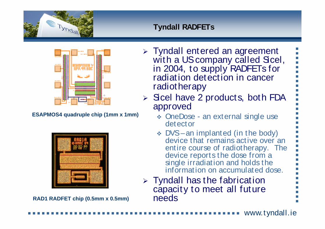
Tyndall RADFETs
Tyndall entered an agreement with a US company called Sicel, in 2004, to supply RADFETs for radiation detection in cancer radiotherapy
Sicel have 2 products, both FDA approved OneDose - an external single use
detector DVS – an implanted (in the body)
device that remains active over an entire course of radiotherapy. The device reports the dose from a single irradiation and holds the information on accumulated dose.
Tyndall has the fabrication capacity to meet all future needs
ESAPMOS4 quadruple chip (1mm x 1mm)
RAD1 RADFET chip (0.5mm x 0.5mm)

www.tyndall.ie
Fabrication of Linear Diode Arrays for Xenics
Xenics Infrared Solutions is involved in a space programme for satellite imaging
Their role is to provide a system that will consist of 4 linear sensor arrays of 512 pixels on 25um pitch and pixel height
Each of the 4 sensors will respond to a different wavelength range Visible (VIS) Near IR (NIR) Shortwave IR1 (SWIR1) Shortwave IR2 (SWIR2)
Xenics are fabricating the SWIR detectors in their proprietary InGaAs process
Tyndall fabricated the VIS and NIR sensors in Silicon
www.tyndall.ie
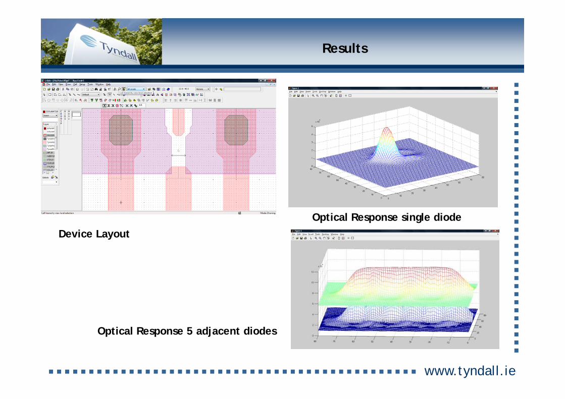
Results
Device LayoutOptical Response single diode
Optical Response 5 adjacent diodes
www.tyndall.ie
Project History
The project history is interesting Tyndall was approached by Xenics and bid for the project in
2008 The bid was unsuccessful and awarded to a commercial foundry In May of 2010 Xenics came back and asked to discuss simply
processing silicon arrays on a batch basis It turned that after 2 years of development the project still had
not got working silicon Tyndall was audited by the Prime Contractor, TNO, on
27/05/2010 Purchase Order 10/06/2010 Silicon deliveries completed 13/09/2010 One delivery of silicon (3 wafers of each) for each of the
wavelengths VIS/NIR met all of Xenics silicon requirements for the project
This included a mask change at Xenics’ request after the first delivery of silicon
www.tyndall.ie
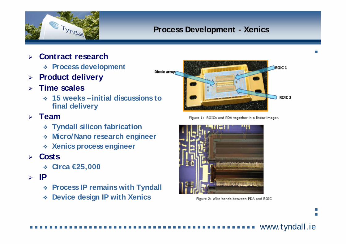
Process Development - Xenics
Contract research Process development
Product delivery Time scales
15 weeks – initial discussions to final delivery
Team Tyndall silicon fabrication Micro/Nano research engineer Xenics process engineer
Costs Circa €25,000
IP Process IP remains with Tyndall Device design IP with Xenics
www.tyndall.ie
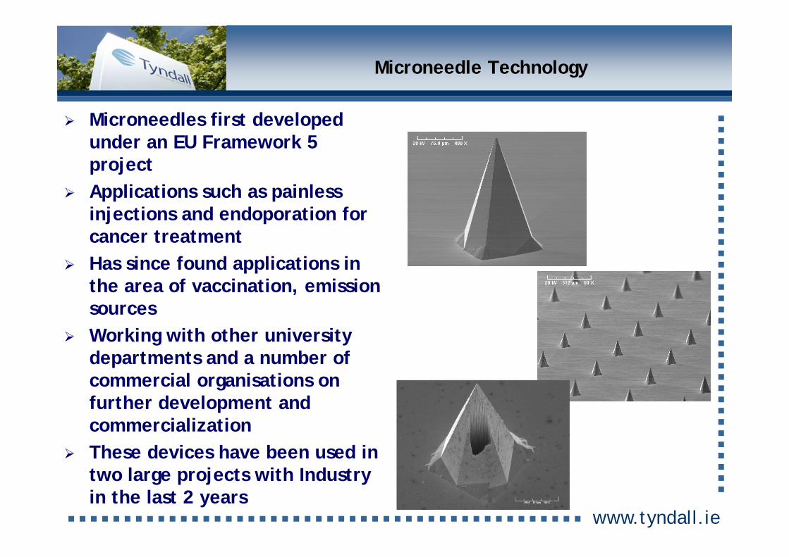
Microneedle Technology
Microneedles first developed under an EU Framework 5 project
Applications such as painless injections and endoporation for cancer treatment
Has since found applications in the area of vaccination, emission sources
Working with other university departments and a number of commercial organisations on further development and commercialization
These devices have been used in two large projects with Industry in the last 2 years
www.tyndall.ie
Industry Engineers in Fabrication
Researchers in residence at Tyndall well documented Also have fabrication engineers in “residence” This facilitated the conversion of a
research/development process to a full production process with all of the documentation and characterization that goes with that
Means that Tyndall not only can offer up through the 9 levels of TRL (mainly level 7) but also up to level level 9 of MRL
www.tyndall.ie
Summary
Tyndall has a range of flexible fabrication facilities to meet a wide cross-section of needs
There are a number of collaborative models that are used for interaction with industry These range from straight contract research to collaborative
arrangements with industry engineers embedded at Tyndall
Companies working with Tyndall get the benefit of all of the background technology available
IP is not an issue as Tyndall has a team experienced in drawing up mutually agreeable terms and conditions
As well as the fabrication facilities there is a wide range of research and characterization laboratories Access to all labs is seamless to the customer


